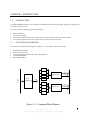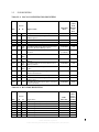
1
PMC-SIO4RS232
User Manual
Preliminary
General Standards Corporation
8302A Whitesburg Drive
Huntsville, AL 35802
Phone: (256) 880-8787
Fax: (256) 880-8788
URL: www.generalstandards.com
E-mail: http://[email protected]/
PREFACE
Copyright © 1998 General Standards Corp.
Additional copies of this manual or other General Standards Corporation literature may be obtained from:
General Standards Corporation
8302A Whitesburg Drive
Huntsville, Alabama 35802
Telephone: (256) 880-8787
Fax: (256) 880-8788
Company URL: www.generalstandards.com
The information in this document is subject to change without notice.
General Standards Corporation makes no warranty of any kind with regard to this material, including, but not limited
to, the implied warranties of merchantability and fitness for a particular purpose. Although extensive editing and
reviews are performed before release to ECO control, General Standards Corporation assumes no responsibility for
any errors that may exist in this document. No commitment is made to update or keep current the information
contained in this document.
General Standards Corporation does not assume any liability arising out of the application or use of any product or
circuit described herein, nor is any license conveyed under any patent right of any rights of others.
General Standards Corporation assumes no responsibility resulting from omissions or errors in this manual, or from
the use of information contained herein.
General Standards Corporation reserves the right to make any changes, without notice, to this product to improve
reliability, performance, function, or design.
All rights reserved
No parts of this document may be copied or reproduced in any form or by any means without prior written consent of
General Standards Corporation.
This user’s manual provides information on the, register level programming, of the PMC-SIO4-RS232 board.
Information required for customized software development.
This manual assumes that the user is familiar with the PCI bus interface specification. In an effort to avoid
redundancy, this manual relies on data books, other manuals, and specifications as indicated in the related
publication
section.
User Manual for the PMC-SIO4-RS232 Card, Revision: B
General Standards Corporation
8302A Whitesburg Drive Huntsville, AL 35802, Phone: (256) 880-8787
III
RELATED PUBLICATIONS
EIA Standard for the RS-422A Interface (EIA order number EIA-RS-422A)
Draft Standard Physical and Environmental Layers for PCI Mezzanine Cards: PMC
Sponsored by the
Bus Architecture Standards Committee
of the IEEE Computer Society
P1386.1/Draft 2.0
April 4,1995
Sponsor Ballot Draft
For questions or comments regarding this draft, please contact either the chair or draft editor of this proposed
standard:
Wayne Fisher
PMC Chair
2001 Logic Drive
San Jose, CA 95124-3456 USA
Ph: 408-369-6250
Fax: 408-371-3382
Em: [email protected]
Dave Moore
PMC Draft Editor
Digital Equipment Corporation
146 Main Street MLO11-4/U32
Maynard, MA 01754-2571 USA
Ph: 408-493-2257
Fax: 408-493-0652
E-mail: [email protected]
PCI Local Bus Specification Revision 2.1 June 1, 1995. Questions regarding the PCI specification be forwarded to:
PCI Special Interest Group
P.O. Box 14070
Portland, OR 97214
(800) 433- 5177 (U.S.)
(503) 797-4207 (International)
(503) 234-6762 (FAX)
Zilog User’s Manual and Product Specifications Databook for the Z16C30 USC requests should be forwarded to:
ZILOG, Inc.
210 East Hacienda Ave.
Campbell, CA 95008-6600
(408) 370-8000
User Manual for the PMC-SIO4-RS232 Card, Revision: B
General Standards Corporation
8302A Whitesburg Drive Huntsville, AL 35802, Phone: (256) 880-8787
IV
TABLE OF CONTENTS
CHAPTER 1: INTRODUCTION................................................................................................................................................. 1
1.0
1.1
1.2
1.3
1.4
1.5
1.6
1.7
1.8
INTRODUCTION ..........................................................................................................................................................1
FUNCTIONAL DESCRIPTION ...................................................................................................................................1
BOARD CONTROL REGISTER...................................................................................................................................2
BOARD STATUS REGISTER......................................................................................................................................2
SYNC WORD SELECTION REGISTERS....................................................................................................................2
DATA RECEPTION......................................................................................................................................................2
DATA TRANSMITION...............................................................................................................................................2
ERROR DETECTION ....................................................................................................................................................2
INTERRUPTS.................................................................................................................................................................3
CHAPTER 2: PCI CONFIGURATION REGISTERS............................................................................................................. 5
2.1
PCI CONFIGURATION REGISTERS..........................................................................................................................5
2.2
PLX REGISTERS............................................................................................................................................................6
2.3
PCI CONFIGURATION REGISTER BIT MAPS........................................................................................................8
2.3.1
PCI Configuration ID Register (Offset 0x00) ....................................................................................................8
2.3.2
PCI Command Register (Offset 0x04).................................................................................................................8
2.3.3
PCI Status Register (Offset 0x06).......................................................................................................................8
2.3.4
PCI Revision ID Register (Offset 0x08) .............................................................................................................9
2.3.5
PCI Class Code Register (Offset 0x09..0B)........................................................................................................9
2.3.6
PCI Cache Line Size Register (Offset 0x0C)......................................................................................................9
2.3.7
PCI Latency Timer Register (Offset 0x0D)........................................................................................................9
2.3.8
PCI Header Type Regis ter (Offset 0x0E) ...........................................................................................................9
2.3.9
PCI Built-In Self Test (BIST) Register (Offset 0x0F) .......................................................................................9
2.3.10
PCI Base Address Register for Memory Access to Runtime Registers (Offset 0x010).............................9
2.3.11
PCI Base Address Register for I/O Access to Runtime Registers (Offset 0x14) ........................................9
2.3.12
PCI Base Address Register for Memory Access to Local Address Space 0 (Offset 0x18).....................10
2.3.13
PCI Base Address Register for Memory Access to Local Address Space 1 (Offset 0x1C)....................10
2.3.14
PCI Base Address Register (Offset 0x20) ......................................................................................................10
2.3.15
PCI Base Address Register (Offset 0x24) ......................................................................................................10
2.3.16
PCI Cardbus CIS Pointer Register (Offset 0x28) ............................................................................................10
2.3.17
PCI Subsystem Vendor ID Register (Offset 0x2C).........................................................................................10
2.3.18
PCI Subsystem ID Register (Offset 0x2E) .......................................................................................................10
2.3.19
PCI Expansion ROM Base Register (Offset 0x30)..........................................................................................10
2.3.20
PCI Interrupt Line Register (Offset 0x3C) .......................................................................................................11
2.3.21
PCI Interrupt Pin Register (Offset 0x3D).........................................................................................................11
2.3.22
PCI Min_Gnt Register (Offset 0x3E) ................................................................................................................11
2.3.23
PCI Max_Lat Register (Offset 0x3F) ................................................................................................................11
2.4
LOCAL CONFIGURATION REGISTERS.................................................................................................................11
2.4.1
Local Address Space 0 Range Register for PCI to Local bus (PCI 0x00)...................................................11
2.4.2
Local Address Space 0 Local Base Address (Re-map) Register for PCI to Local Bus (PCI 0x04) .........11
2.4.3
Mode/Arbitration Register (PCI 0x08).............................................................................................................11
2.4.4
Big/Little Endian Descriptor Register (PCI 0x0C) ..........................................................................................13
2.4.5
Local Expansion ROM Range Register for PCI to Local Bus (PCI 0x10)....................................................13
User Manual for the PMC-SIO4-RS232 Card, Revision: B
General Standards Corporation
8302A Whitesburg Drive Huntsville, AL 35802, Phone: (256) 880-8787
V
2.4.6
Local Expansion ROM Local Base Address (Re-map) register for PCI to Local Bus and BREQo Control
(PCI 0x14)...............................................................................................................................................................................13
2.4.7
Local Address Space 0/Expansion ROM Bus Region Descriptor Register (PCI 0x18)............................13
2.4.8
Local Range register for Direct Master to PCI (PCI 0x1C)............................................................................13
2.4.9
Local Bus Base Address register for Direct Master to PCI Memory (PCI 0x20).......................................14
2.4.10
Local Base Address for Direct Master to PCI IO/CFG Register (PCI 0x24)...............................................14
2.4.11
PCI Base Address (Re-map) register for Direct Master to PCI Memory (PCI 0x28).................................14
2.4.12
PCI Configuration Address Register for Direct Master to PCI IO/CFG (PCI 0x2C)..................................14
2.4.13
Local Address Space 1 Range Register for PCI to Local Bus (PCI 0xF0) ..................................................14
2.4.14
Local Address Space 1 Local Base Address (Remap) Register (PCI 0xF4)...............................................14
2.4.15
Local Address Space 1 Bus Region Descriptor Register (PCI 0xF8)..........................................................15
2.5
RUNTIME REGISTERS ..............................................................................................................................................15
2.5.1
Mailbox Register 0 (PCI 0x40)...........................................................................................................................15
2.5.2
Mailbox Register 1 (PCI 0x44)...........................................................................................................................15
2.5.3
Mailbox Register 2 (PCI 0x48)...........................................................................................................................15
2.5.4
Mailbox Register 3 (PCI 0x4C) ..........................................................................................................................15
2.5.5
Mailbox Register 4 (PCI 0x50)...........................................................................................................................15
2.5.6
Mailbox Register 5 (PCI 0x54)...........................................................................................................................15
2.5.7
Mailbox Register 6 (PCI 0x58)...........................................................................................................................15
2.5.8
Mailbox Register 7 (PCI 0x5C) ..........................................................................................................................15
2.5.9
PCI to Local Doorbell Register Description (PCI 0x60).................................................................................15
2.5.10
Local to PCI Doorbell Register Description (PCI 0x64).................................................................................16
2.5.11
Interrupt Control /Status (PCI 0x68) ................................................................................................................16
2.5.12
Serial EEPROM Control, PCI Command Codes, User I/O Control, Init Control Register (PCI 0x6C).....16
2.5.13
PCI Permanent Configuration ID Register (PCI 0x70) ..................................................................................17
2.5.14
PCI Permanent Revision ID Register (PCI 0x74) ...........................................................................................17
2.6
LOCAL DMA REGISTERS ........................................................................................................................................17
2.6.1
DMA Channel 0 Mode Register (PCI 0x80)....................................................................................................17
2.6.2
DMA Channel 0 PCI Address Register (PCI 0x84)........................................................................................17
2.6.3
DMA Channel 0 Local Address Register (PCI 0x88) ....................................................................................17
2.6.4
DMA Channel 0 Transfer Size (Bytes) Register (PCI 0x8C).........................................................................17
2.6.5
DMA Channel 0 Descriptor Pointer Register (PCI 0x90)..............................................................................17
2.6.6
DMA Channel 1 Mode Register (PCI 0x94)....................................................................................................18
2.6.7
DMA Channel 1 PCI Data Address Register (PCI 0x98) ..............................................................................18
2.6.8
DMA Channel 1 Local Data Address Register (PCI 0x9C) ..........................................................................18
2.6.9
DMA Channel 1 Transfer Size (bytes) register (PCI 0xA0)..........................................................................18
2.6.10
DMA Channel 1 Descriptor Pointer Register (PCI 0xA4).............................................................................18
2.6.11
DMA Command/Status Register (PCI 0xA8) .................................................................................................18
2.6.12
DMA Channel 1 Command/Status Register 0 (PCI 0xA8)............................................................................19
2.6.13
DMA Arbitration Register 1 same as Mode /Arbitration Register at address (PCI 0xAC).....................19
2.7
MESSAGING QUEUE REGISTERS...........................................................................................................................19
2.7.1
Outbound Post List FIFO Interrupt Status Register (PCI 0x30) ..................................................................19
2.7.2
Outbound Post List FIFO Interrupt Status Register (PCI 0x34) ..................................................................19
2.7.3
Inbound Queue Port Register (PCI 0x40)........................................................................................................19
2.7.4
Outbound Queue Port Register (PCI 0x44).....................................................................................................19
2.7.5
Messaging Queue Configuration Register (PCI 0xC0) .................................................................................20
2.7.6
Queue Base Address Register (PCI 0xC4)......................................................................................................20
2.7.7
Inbound Free Head Pointer Register (PCI 0xC8)............................................................................................20
2.7.8
Inbound Free Head Tail Register (PCI 0xCC).................................................................................................20
2.7.9
Inbound Post Head Pointer Register (PCI 0xD0)...........................................................................................20
2.7.10
Inbound Post Tail Pointer Register (PCI 0xD4)..............................................................................................20
2.7.11
Outbound Free Head Pointer Register (PCI 0xD8) ........................................................................................20
2.7.12
Outbound Free Tail Pointer Register (PCI 0xDC) ..........................................................................................20
User Manual for the PMC-SIO4-RS232 Card, Revision: B
General Standards Corporation
8302A Whitesburg Drive Huntsville, AL 35802, Phone: (256) 880-8787
VI
2.7.13
Outbound Post Head Pointer Register (PCI 0xE0).........................................................................................20
2.7.14
Outbound Post Tail Pointer Register (PCI 0xE4) ...........................................................................................21
2.7.15
Queue Status/Control Register (PCI 0xE8) .....................................................................................................21
2.8
PCI CONFIGURATION REGISTER BIT DESCRIPTIONS.....................................................................................21
2.8.1
PCI Configuration ID Register (Offset 0x00) ..................................................................................................21
2.8.2
PCI Command Register (Offset 0x04)...............................................................................................................21
2.8.3
PCI Status Register (Offset 0x06).....................................................................................................................22
2.8.4
PCI Revision ID Register (Offset 0x08) ...........................................................................................................23
2.8.5
PCI Class Code Register (Offset 0x09 - 0B) ....................................................................................................23
2.8.6
PCI Cache Line Size Register (Offset 0x0C)....................................................................................................23
2.8.7
PCI Latency Timer Register (Offset 0x0D)......................................................................................................23
2.8.8
PCI Header Type Register (Offset 0x0E) .........................................................................................................23
2.8.9
PCI Built-In Self Test (BIST) Register (Offset 0x0F) .....................................................................................23
2.8.10
PCI Base Address Register for Memory Access to Runtime Registers (Offset 0x010)...........................23
2.8.11
PCI Base Address Register for I/O Access to Runtime Registers (Offset 0x14) ......................................24
2.8.12
PCI Base Address Register for Memory Access to Local Address Space 0 (Offset 0x18).....................24
2.8.13
PCI Base Address Register for Memory Accesses to Local Address Space 1 (Offset 0x1C)................25
2.8.14
PCI Base Address Register (Offset 0x20) ......................................................................................................25
2.8.15
PCI Base Address Register (Offset 0x24) ......................................................................................................25
2.8.16
PCI Base Cardbus CIS Pointer Register (Offset 0x28)...................................................................................25
2.8.17
PCI Subsystem Vendor ID Register (Offset 0x2C).........................................................................................25
2.8.18
PCI Subsystem ID Register (Offset 0x2E) .......................................................................................................25
2.8.19
PCI Expansion ROM Base Register (Offset 0x30)..........................................................................................25
2.8.20
PCI Interrupt Line Register (Offset 0x3C) .......................................................................................................25
2.8.21
PCI Interrupt Pin Register (Offset 0x3D).........................................................................................................26
2.8.22
PCI Min_Gnt Register (Offset 0x3E) ................................................................................................................26
2.8.23
PCI Max_Lat Register (Offset 0x3F) ................................................................................................................26
2.9
LOCAL CONFIGURATION REGISTERS BIT DESCRIPTIONS ....................................................................................26
2.9.1
Local Address Space 0 Range Register for PCI to Local bus (PCI 0x00)...................................................26
2.9.2
Local Address Space 0 Local Base Address (Re-map) Register for PCI to Local Bus (PCI 0x04) .........27
2.9.3
Mode/Arbitration Register (PCI 0x08).............................................................................................................27
2.9.4
Local Register (PCI 0x0C)..................................................................................................................................28
2.9.5
Local Expansion ROM Range Register for PCI to Local Bus (PCI 0x10)....................................................29
2.9.6
Local Expansion ROM Local Base Address (Re-map) register for PCI to Local Bus and BREQo Control
(PCI 0x14)...............................................................................................................................................................................29
2.9.7
Local Bus Region Descriptor for PCI to Local Accesses Register (PCI 0x18) ..........................................29
2.9.8
Local Range register for Direct Master to PCI (PCI 0x1C)............................................................................30
2.9.9
Local Bus Base Address register for Direct Master to PCI Memory (PCI 0x20).......................................31
2.9.10
Local Base Address for Direct Master to PCI IO/CFG Register (PCI 0x24)...............................................31
2.9.11
PCI Base Address (Re-map) register for Direct Master to PCI (PCI 0x28).................................................31
2.9.12
PCI Configuration Address Register for Direct Master to PCI IO/CFG (PCI 0x2C)..................................32
2.9.13
Local Address Space 1 Range Register for PCI to Local Bus (PCI 0xF0) ..................................................32
2.9.14
Local Address Space 1 Local Base Address (Remap) Register (PCI 0xF4)...............................................32
2.9.15
Local Address Space 1 Bus Region Descriptor Register (PCI 0xF8)..........................................................33
2.10 SHARED RUNTIME REGISTERS BIT DESCRIPTIONS...............................................................................................33
2.10.1
Mailbox Register 0 (PCI 0x40)...........................................................................................................................33
2.10.2
Mailbox Register 1 (PCI 0x44)...........................................................................................................................34
2.10.3
Mailbox Register 2 (PCI 0x48)...........................................................................................................................34
2.10.4
Mailbox Register 3 (PCI 0x4C) ..........................................................................................................................34
2.10.5
Mailbox Register 4 (PCI 0x50)...........................................................................................................................34
2.10.6
Mailbox Register 5 (PCI 0x54)...........................................................................................................................34
2.10.7
Mailbox Register 6 (PCI 0x58)...........................................................................................................................34
2.10.8
Mailbox Register 7 (PCI 0x5C) ..........................................................................................................................34
User Manual for the PMC-SIO4-RS232 Card, Revision: B
General Standards Corporation
8302A Whitesburg Drive Huntsville, AL 35802, Phone: (256) 880-8787
VII
2.10.9
PCI to Local Doorbell Register Description (PCI 0x60).................................................................................34
2.10.10
Local to PCI Doorbell Register Description (PCI 0x64) ............................................................................34
2.10.11
Interrupt Control /Status (PCI 0x68)............................................................................................................34
2.10.12
EEPROM Control, PCI Command Codes, User I/O Control, Init Control Register (PCI 0x6C) ...........36
2.10.13
PCI Permanent Configuration ID Register (PCI 0x70)...............................................................................37
2.10.14
PCI Permanent Revision ID Register (PCI 0x74)........................................................................................37
2.11 LOCAL DMA REGISTERS ........................................................................................................................................37
2.11.1
DMA Channel 0 Mode Register (PCI 0x80)....................................................................................................37
2.11.2
DMA Channel 0 PCI Address Register (PCI 0x84)........................................................................................38
2.11.3
DMA Channel 0 Local Address Register (PCI 0x88) ....................................................................................38
2.11.4
DMA Channel 0 Transfer Size (Bytes) Register (PCI 0x8C).........................................................................38
2.11.5
DMA Channel 0 Descriptor Pointer Register (PCI 0x90)..............................................................................38
2.11.6
DMA Channel 1 Mode Register (PCI 0x94)....................................................................................................39
2.11.7
DMA Channel 1 PCI Data Address Register (PCI 0x98) ..............................................................................39
2.11.8
DMA Channel 1 Local Data Address Register (PCI 0x9C) ..........................................................................39
2.11.9
DMA Channel 1 Transfer Size (bytes) register (PCI 0xA0)..........................................................................40
2.11.10
DMA Channel 1 Descriptor Pointer Register (PCI 0xA4) ........................................................................40
2.11.11
DMA Command/Status Register (PCI 0xA8).............................................................................................40
2.11.12
DMA Command/Status Register (PCI 0xA9).............................................................................................40
2.11.13
DMA Arbitration Register 0 (PCI 0xAC)....................................................................................................41
2.11.14
DMA Threshold Register 1 (PCI 0xB0).......................................................................................................41
2.12 MESSAGING QUEUE REGISTERS...........................................................................................................................41
2.12.1
Outbound Post List FIFO Interrupt Status Register (PCI 0x30) ..................................................................41
2.12.2
Outbound Post List FIFO Interrupt MASK Register (PCI 0x34).................................................................41
2.12.3
Inbound Queue Port Register (PCI 0x40 while QSR D0=1) ..........................................................................42
2.12.4
Outbound Queue Port Register (PCI 0x44 while QSR D0=1) .......................................................................42
2.12.5
Messaging Queue Configuration Register (PCI 0xC0) .................................................................................42
2.12.6
Queue Base Address Register (PCI 0xC4)......................................................................................................42
2.12.7
Inbound Free Head Pointer Register (PCI 0xC8)............................................................................................43
2.12.8
Inbound Free Head Tail Register (PCI 0xCC).................................................................................................43
2.12.9
Inbound Post Head Pointer Register (PCI 0xD0)...........................................................................................43
2.12.10
Inbound Post Tail Pointer Register (PCI 0xD4) .........................................................................................43
2.12.11
Outbound Free Head Pointer Register (PCI 0xD8)....................................................................................43
2.12.12
Outbound Free Tail Pointer Register (PCI 0xDC)......................................................................................43
2.12.13
Outbound Post Head Pointer Register (PCI 0xE0) ....................................................................................44
2.12.14
Outbound Post Tail Pointer Register (PCI 0xE4).......................................................................................44
2.12.15
Queue Status/Control Register (PCI 0xE8).................................................................................................44
CHAPTER 3: LOCAL SPACE REGISTERS..........................................................................................................................45
3.0
REGISTER MAP..........................................................................................................................................................45
3.1
BIT MAP FOR LOCAL SPACE REGISTERS ..........................................................................................................46
3.1.0
FIRMWARE REVISION: (loc 0x00) ................................................................................................................46
3.1.1
BOARD CONTROL: (loc 0x04).........................................................................................................................46
3.1.2
CHANNEL 1 Tx ALMOST: (LOC 0x10)...........................................................................................................46
3.1.3
CHANNEL 1 RX ALMOST: (LOC 0x14) .........................................................................................................46
3.1.4
CHANNEL 1 FIFO: (LOC 0x18).........................................................................................................................47
3.1.5
CHANNEL 1 CONTROL/STATUS: (LOC 0x1C)............................................................................................47
3.1.6
CHANNEL 2 Tx ALMOST: (LOC 0x20)...........................................................................................................48
3.1.7
CHANNEL 2 RX ALMOST: (LOC 0x24) .........................................................................................................48
3.1.8
CHANNEL 2 FIFO: (LOC 0x28).........................................................................................................................48
3.1.9
CHANNEL 2 CONTROL/STATUS: (LOC 0x2C)...........................................................................................48
3.1.10
CHANNEL 3 TX ALMOST: (LOC 0x30) .........................................................................................................49
3.1.11
CHANNEL 3 RX Almost: (LOC 0x34)..............................................................................................................49
User Manual for the PMC-SIO4-RS232 Card, Revision: B
General Standards Corporation
8302A Whitesburg Drive Huntsville, AL 35802, Phone: (256) 880-8787
VIII
3.1.12
CHANNEL 3 FIFO: (LOC 0x38).........................................................................................................................49
3.1.13
CHANNEL 3 CONTROL/STATUS: (LOC 0x3C)............................................................................................49
3.1.14
CHANNEL 4 TX ALMOST: (LOC 0x40) .........................................................................................................50
3.1.15
CHANNEL 4 RX ALMOST: (LOC 0x44) .........................................................................................................50
3.1.16
CHANNEL 4 FIFO: (LOC 0x48).........................................................................................................................50
3.1.17
CHANNEL 4 CONTROL/STATUS: (LOC 0x4C)............................................................................................51
3.1.18
CHANNEL 1 SYNC DETECTED: (LOC 0x50).................................................................................................51
3.1.19
CHANNEL 2 SYNC DETECTED: (LOC 0x54).................................................................................................52
3.1.20
CHANNEL 3 SYNC DETECTED: (LOC 0x58).................................................................................................52
3.1.21
CHANNEL 4 SYNC DETECTED: (LOC 0x5C) ................................................................................................52
3.1.22
INTERRUPT CONTROL: (LOC 0x60) ..............................................................................................................52
3.1.23
INTERRUPT STATUS: (LOC 0x64) .................................................................................................................53
3.1.24
CHANNEL 1 USC: (LOC 0x100 to 0x17E) ........................................................................................................53
3.1.25
CHANNEL 2 USC: (LOC 0x200 to 0x27E)........................................................................................................53
3.1.26
CHANNEL 3 USC: (LOC 0x300 0x37E).............................................................................................................53
3.1.27
CHANNEL 4 USC: (LOC 0x400 to 0x47E) ........................................................................................................53
3.2
SERIAL CONTROLLER REGISTERS .......................................................................................................................54
3.2.1
3.2.1.1
3.2.1.2
3.2.2
3.2.2.1
3.2.2.2
3.2.3
3.2.3.1
3.2.3.2
3.2.4
3.2.4.1
3.2.5
3.2.5.1
3.2.5.2
3.3.6
Channel Command/Address Register (CCAR)................................................................................................54
Low: (LOC 0xn00).....................................................................................................................................54
High: (LOC: 0xn02)....................................................................................................................................54
Channel Mode Register (CMR)........................................................................................................................55
Low: (LOC 0xn04)......................................................................................................................................55
High: (LOC 0xn06)......................................................................................................................................55
Channel Command/Status Register (CCSR) .....................................................................................................56
Low: (LOC 0xn08)......................................................................................................................................56
High: (LOC 0xn0A).....................................................................................................................................56
Channel Control Register (CCR) ......................................................................................................................56
Low: (LOC 0xn0C) .....................................................................................................................................57
Primary Reserved Register (RESERVED)........................................................................................................57
Low: (LOC 0xn10)......................................................................................................................................57
High: (LOC 0xn12)......................................................................................................................................57
Secondary Reserved Register (RESERVED) ..................................................................................................57
3.3.6.1
3.3.6.2
3.3.7
Low: (LOC 0xn14)......................................................................................................................................57
High: (LOC 0xn16)......................................................................................................................................57
Test Mode Data Register (TMDR)..................................................................................................................57
3.3.7.1 Low: (LOC: 0xn18)........................................................................................................................................57
3.3.7.2
High: (LOC 0xn1A).....................................................................................................................................58
3.3.8
Test Mode Control Register (TMCR) .............................................................................................................58
3.3.8.1
3.3.8.2
3.3.9
Low: (LOC 0xn1C) .....................................................................................................................................58
High: (LOC 0xn1E) .....................................................................................................................................58
Clock Mode Control Register (CMCR) ...........................................................................................................58
3.3.9.1
3.3.9.2
3.3.10
Low: (LOC 0xn20)......................................................................................................................................59
High: (LOC 0xn22)......................................................................................................................................59
Hardware Configuration Register (HCR) ........................................................................................................60
3.3.10.1 Low: (LOC 0xn24)..........................................................................................................................................60
3.3.10.2 High: (LOC 0xn26)..........................................................................................................................................60
3.3.11 Interrupt Vector Register (IVR)............................................................................................................................60
3.3.11.1 Low: (LOC 0xn28)..........................................................................................................................................60
3.3.11.2 High: (LOC 0xn2A).........................................................................................................................................60
3.3.12 I/O Control Register (IOCR) .................................................................................................................................61
3.3.12.1 Low: (LOC 0xn2C) .........................................................................................................................................61
3.3.12.2 High: (LOC 0xn2E) .........................................................................................................................................61
3.3.13 interrupt Control Register (ICR)..............................................................................................................................62
User Manual for the PMC-SIO4-RS232 Card, Revision: B
General Standards Corporation
8302A Whitesburg Drive Huntsville, AL 35802, Phone: (256) 880-8787
IX
3.3.13.1 Low: (LOC 0xn30)..........................................................................................................................................62
3.3.13.2 High: (LOC 0xn32)..........................................................................................................................................62
3.3.14 Daisy-Chain Control Register (DCCR)...................................................................................................................62
3.3.14.1 Low: (LOC: 0xn34)........................................................................................................................................62
3.3.14.2 High RW: (LOC 0xn36) ..................................................................................................................................63
3.3.15 Miscellaneous Interrupt Status Register (MISR).............................................................................................63
3.3.15.1 Low: (LOC 0xn38)..........................................................................................................................................63
3.3.15.2 High: (LOC 0xn3A).........................................................................................................................................63
3.3.16 status interrupt control Register (SICR).............................................................................................................63
3.3.16.1 Low: (LOC 0xn3C) .........................................................................................................................................63
3.3.16.2 High: (LOC 0xn3E) .........................................................................................................................................64
3.3.17 Tx/Rx Data Register (RDR/TDR)..........................................................................................................................64
3.3.17.1 Low: (LOC 0xn40)..........................................................................................................................................64
3.3.17.2 High: (LOC 0xn42)..........................................................................................................................................64
3.3.18 Receiver Mode Register (RMR)...........................................................................................................................64
3.3.18.1 Low: (LOC 0xn44)..........................................................................................................................................65
3.3.18.2 High: (LOC 0xn46)..........................................................................................................................................65
3.3.19 Receive Command Status Register (RCSR)...........................................................................................................65
3.3.19.1 Low: (LOC 0xn48)..........................................................................................................................................65
3.3.19.2 High: (LOC 0xn4A).........................................................................................................................................66
3.3.20 Receive Interrupt Control Register (RICR).........................................................................................................66
3.3.20.1 Low: (LOC 0xn4C) .........................................................................................................................................66
3.3.20.2 High: (LOC 0xn4E) .........................................................................................................................................66
3.3.21 Receive Sync Register (RSR) ..................................................................................................................................66
3.3.21.1 Low: (LOC 0xn50)..........................................................................................................................................67
3.3.21.2 High: (LOC 0xn52)..........................................................................................................................................67
3.3.22 Receive Count Limit Register (RCLR)....................................................................................................................67
3.3.22.1 Low: (LOC 0xn54)..........................................................................................................................................67
3.3.22.2 High: (LOC 0xn56)..........................................................................................................................................67
3.3.23 Receive Character Count Register (RCCR) ...........................................................................................................67
3.3.23.1 Low: (LOC 0xn58)..........................................................................................................................................67
3.3.23.2 High: (LOC 0xn5A).........................................................................................................................................67
3.3.24 Time Constant 0 Register (TC0R)...........................................................................................................................67
3.3.24.1 Low: (LOC 0xn5C) .........................................................................................................................................67
3.3.24.2 High: (LOC 0xn5E) .........................................................................................................................................67
3.3.25 Transmit Mode Register (TMR) .............................................................................................................................67
3.3.25.1 Low: (LOC 0xn64)..........................................................................................................................................67
3.3.25.2 High: (LOC 0xn66)..........................................................................................................................................68
3.3.26 Transmit Command/Status Register (TCSR).........................................................................................................68
3.3.26.1 Low: (LOC 0xn68)..........................................................................................................................................68
3.3.26.2 High: (LOC 0xn6A).........................................................................................................................................68
3.3.27 Transmit Interrupt Control Register (TICR)..........................................................................................................69
3.3.27.1 Low: (LOC 0xn6C) .........................................................................................................................................69
3.3.27.2 High: (LOC 0xn6E) .........................................................................................................................................69
3.3.28 Transmit Sync Register (TSR).................................................................................................................................69
3.3.28.1 Low: (LOC 0xn70)..........................................................................................................................................69
3.3.28.2 High: (LOC 0xn72)..........................................................................................................................................69
3.3.29 Transmit Count Limit Register (TCLR) ..................................................................................................................69
3.3.29.1 Low: (LOC 0xn74)..........................................................................................................................................70
3.3.29.2 High: (LOC 0xn76)..........................................................................................................................................70
3.3.30 Transmit Character Count Register (TCCR)..........................................................................................................70
3.3.30.1 Low: (LOC 0xn78)..........................................................................................................................................70
3.3.30.2 High: (LOC 0xn7A).........................................................................................................................................70
User Manual for the PMC-SIO4-RS232 Card, Revision: B
X
General Standards Corporation
8302A Whitesburg Drive Huntsville, AL 35802, Phone: (256) 880-8787
3.3.31 Time Constant 1 Register (TC1R)...........................................................................................................................70
3.3.31.1 Low: (LOC 0xn7C) .........................................................................................................................................70
3.3.31.2 High: (LOC 0xn7E) .........................................................................................................................................70
CHAPTER 4: HARDWARE CONFIGURATION .................................................................................................................71
4.0
4.1
4.2
4.3
THE ON-BOARD MASTER & TRANSMIT/RECEIVE CLOCKS ........................................................................71
EEPROM JUMPER (J12).............................................................................................................................................71
CABLE INTERFACE CONNECTIONS.....................................................................................................................71
THE ZILOG CLOCK SELECT JUMPERS (J3, J4, J7, & J8) ...................................................................................72
User Manual for the PMC-SIO4-RS232 Card, Revision: B
General Standards Corporation
8302A Whitesburg Drive Huntsville, AL 35802, Phone: (256) 880-8787
XI
CHAPTER 1: INTRODUCTION
1.0
INTRODUCTION
The PMC-SI04-RS232 interface card is capable of transmitting and receiving serial data, generating interrupts, and
providing loop-back testing.
This card provides the following specific functionality’s:
•
•
•
•
1.1
PMC bus Interface:
Interrupt functionality
FIFOs are provided for data transmit and for data receive to increase the size of the receive buffers.
User interface signals connections are provided via connectors on the front panel.
FUNCTIONAL DESCRIPTION
As shown in the functional block diagram (see Figure 1.1-1), this board includes the following:
•
•
•
•
•
PMC Bus Slave Interface
RS 232 ECL Transceivers
2 Universal Serial Controllers (USC), The (Zilog ZI6C30s)
Transmit FIFO Buffers
Receive FIFO Buffers
Ch1Tx
Ch1Rx
CH 1
DUAL USC
Ch2Tx
P
M
C
PMC
INTERFACE
8
CH 2
Ch2Rx
LD
8
Ch3Tx
CH 3
Ch3Rx
Ch4Tx
DUAL USC
C
A
B
L
E
S
CH 4
8
Ch4Rx
Figure 1.1-1: Functional Block Diagram
User Manual for the PMC-SIO4-RS232 Card, Revision: B
General Standards Corporation
8302A Whitesburg Drive Huntsville, AL 35802, Phone: (256) 880-8787
1
1.2
BOARD CONTROL REGISTER
The board control register will provide configuration for the PMC/DMA request priorities.
1.3
BOARD STATUS REGISTER
The board status register will provide status of the board (for future expansion).
1.4
SYNC WORD SELECTION REGISTERS
The sync word selection registers are used to provide an interrupt upon the reception of a particular character on a
particular channel. This character is software programmable.
1.5
DATA RECEPTION
Data is received into the Zilog Z16C30, after which the software may retrieve the data from the Z16C30 or have the
data buffered into the main Rx FIFOs and retrieved by the software at a latter time, depending on how the Z16C30 has
been initialized.
1.6
DATA TRANSMITION
Data is placed into the Zilog Z16C30 or buffered into the main Tx FIFOs, depending on how the Z16C30 has been
initialized. The Zilog can transmit and receive in any of several serial protocols.
•
•
•
•
•
•
•
•
•
1.7
Asynchronous
External Sync
Isochronous
Asynchronous with Code Violations
Monosynchronous
Bisynchronous
HDLC
SDLC
+ more
ERROR DETECTION
By utilizing the features of the Z16C30, various forms of error detection are built into the board; the following are
some of the methods of error detection available:
•
•
•
•
Parity error detection
CRC error detection
Rx overrun
Tx underrun
User Manual for the PMC-SIO4-RS232 Card, Revision: B
General Standards Corporation
8302A Whitesburg Drive Huntsville, AL 35802, Phone: (256) 880-8787
2
1.8
INTERRUPTS
Interrupts will be provided for the following conditions:
•
•
•
•
•
•
•
•
•
•
•
DMA Complete
Sync word detected
Tx FIFO Almost Empty
Rx FIFO Almost Full
Exited Hunt
Idle Rcvd
Break/Abort
Rx Bound
Abort/Parity Error
Rx Overrun
Plus many others
User Manual for the PMC-SIO4-RS232 Card, Revision: B
General Standards Corporation
8302A Whitesburg Drive Huntsville, AL 35802, Phone: (256) 880-8787
3
User Manual for the PMC-SIO4-RS232 Card, Revision: B
General Standards Corporation
8302A Whitesburg Drive Huntsville, AL 35802, Phone: (256) 880-8787
4
CHAPTER 2: PCI CONFIGURATION REGISTERS
2.1
PCI CONFIGURATION REGISTERS
Table 2.1-1:
PCI Configuration Registers Description
Local
Side
Offset
Addr
0x00
Size
D32
R
yes
0x04
D32
yes
0x08
D32
yes
0x0C
D32
yes
0x10
D32
yes
0x14
D32
yes
0x18
D32
yes
0x1C
0x20
0x24
0x28
0x2C
0x30
D32
D32
D32
D32
D32
D32
yes
yes
yes
yes
yes
yes
0x34
0x38
0x3C
D32
D32
D32
yes
yes
yes
Device ID/Vendor ID
Value after
Reset
0x908010B5
PCI
CFG
register
address
0x00
Status/Command
0x02800017
0x04
Class Code/Revision ID
0x0680003
0x08
BIST/Header Type/Latency Timer/Cache Line
Size
PCI Base Address for Memory Mapped
Runtime Registers
PCI Base Address for 1 for I/O Mapped
Configuration Registers
PCI Base Address 2 for Local Address Space 0
0x00002008
0x0C
PCI Base Address 3 for Local Address Space 1
Unused Base Address
Unused Base Address
Cardbus CIS Pointer (Not Supported)
Subsystem ID/Subsystem Vendor ID
PCI Base Address to Local Expansion ROM
0x00000000
0x00000000
0x00000000
0x908010B5
0x908010B5
0x00000000
0x1C
0x20
0x24
0x28
0x2C
0x30
Reserved
Reserved
Max_lat/Min_Gnt/Interrupt Pin/Interrupt Line
0x00000000
0x00000000
0x0000010A
0x34
0x38
0x3C
Access
W
Local
Bus
Bit
Dep.
Local
Bus
Bit
Dep.
Bit
Dep.
Bit
Dep.
Bit
Dep.
no
no
no
no
no
Bit
Dep.
no
no
Local
Bus
Register Name
0x10
0x14
0x18
User Manual for the PMC-SIO4-RS232 Card, Revision: B
General Standards Corporation
8302A Whitesburg Drive Huntsville, AL 35802, Phone: (256) 880-8787
5
2.2
PLX REGISTERS
Table 2.2-1: LOCAL CONFIGURATION REGISTERS
Access
Size
R
D32
D32
Value after
Reset
Offset
From
Runtime
PCI
Base
W
Register Name
yes
yes
yes
yes
0xFFF00000
0x00000000
0x00
0x04
D32
D32
D32
D32
yes
yes
yes
yes
0xFFF00000
0x00000000
0x08
0x0C
0x10
0x14
D32
yes
no
no
yes
Bit
Dep.
yes
D32
yes
0x40030003
(Cx Mode)
0x00000000
0x1C
D32
yes
0x20
yes
0x00000000
0x24
D32
yes
0x00000000
0x28
D32
yes
0x00000000
0x2C
D32
D32
yes
yes
yes
yes
0x00000000
0x00000000
0x170
0x174
D32
yes
yes
Local Base Address for Direct Master to PCI
Memory
Local Base Address for Direct Master to PCI
Memory IO/CFG
PCI Base Address (Re-map) for Direct Master
to PCI
PCI Configuration Address Register for Direct
Master to PCI IO/CFG
Range for PCI to Local Address Space 1
Local Base Address (Remap) for PCI to Local
Address Space 1
Local Bus Region Descriptor (Space 1) for PCI
to Local Accesses
0x00000000
D32
Bit
Dep.
Bit
Dep.
Bit
Dep.
Bit
Dep.
yes
Range for PCI to Local Address Space 0
Local Base Address (Re-map) for PCI to Local
Address Space 0
Mode Arbitration
Big/Little Endian Descriptor
Range for PCI to Local Expansion ROM
Local Base Address (Re-map) for PCI to Local
Expansion ROM and BREQo control
Bus Region Descriptions for PCI Local
Accesses
Range for Direct Master to PCI
0x00000000
0x178
0x18
Table 2.2-2: RUN TIME REGISTERS
Access
Size
D32
D32
D32
D32
D32
D32
D32
R
yes
yes
yes
yes
yes
yes
yes
W
yes
yes
yes
yes
yes
yes
yes
Register Name
Mailbox Register 0 (see note 1)
Mailbox Register 1 (see note 1)
Mailbox Register 2
Mailbox Register 3
Mailbox Register 4
Mailbox Register 5
Mailbox Register 6
Value
after reset
0x00000000
0x00000000
0x00000000
0x00000000
0x00000000
0x00000000
0x00000000
User Manual for the PMC-SIO4-RS232 Card, Revision: B
General Standards Corporation
8302A Whitesburg Drive Huntsville, AL 35802, Phone: (256) 880-8787
Offset
From
Runtime
PCI Base
0x40
0x44
0x48
0x4C
0x50
0x54
0x58
6
D32
D32
D32
D32
yes
yes
yes
yes
D32
yes
D32
yes
D32
yes
D32
yes
D32
yes
yes
yes
yes
Bit
Dep.
Bit
Dep.
Bit
Dep.
Bit
Dep.
Bit
Dep.
Bit
Dep.
Mailbox Register 7
PCI to Local Doorbell Register
Local to PCI Doorbell Register
Interrupt Control/Status
0x00000000
0x00000000
0x00000000
0x00000000
0x5C
0x60
0x64
0x68
EEPROM Control, PCI Command Codes, User
I/O Control, Init Control
Device ID/Vendor ID
0x001767E
0x6C
0x00
0x70
Unused/Revision ID
0x00
0x74
Mailbox Register 0 (see note 1)
0x00
0x78
Mailbox Register 1 (see note 1)
0x00
0x7C
Table 2.2-3: DMA REGISTERS
Access
Size
R
W
Register Name
D32
yes
yes
DMA Ch 0 Mode
D32
D32
D32
D32
D32
yes
yes
yes
yes
yes
yes
yes
yes
yes
yes
DMA Ch 0 PCI Address
DMA Ch 0 Local Address
DMA Ch 0 Transfer Byte Count
DMA Ch 0 Descriptor Pointer
DMA Ch 1 Mode
D32
D32
D32
D32
D32
yes
yes
yes
yes
D32
yes
DMA Ch 1 PCI Address
DMA Ch 1 Local Address
DMA Ch 1 Transfer Byte Count
DMA Ch 1 Descriptor Pointer
Reserved/DMA Ch 1Command/Status
Register/DMA Ch 0 Command/Status
Mode/ Arbitration Register
D32
yes
yes
yes
yes
yes
Bit
Dep.
Bit
Dep.
Bit
Dep.
DMA Threshold Register
Value after
Reset
Offset
From
Runtime
PCI
Base
0x00000003
(Cx and Jx
modes)
0x00000000
0x00000000
0x00000000
0x00000000
0x00000003
(Cx and Jx
modes)
0x00000000
0x00000000
0x00000000
0x00000000
0x00000010
0x80
0x98
0x9C
0xA0
0xA4
0xA8
0x00000000
0xAC
0x00000000
0xB0
Value
Offset
From
Runtime
0x84
0x88
0x8C
0x90
0x94
Table 2.2-3: MESSAGING QUEUE REGISTERS
Access
User Manual for the PMC-SIO4-RS232 Card, Revision: B
General Standards Corporation
8302A Whitesburg Drive Huntsville, AL 35802, Phone: (256) 880-8787
7
Size
D32
D32
D32
D32
D32
D32
D32
D32
D32
D32
D32
D32
D32
D32
R
yes
yes
yes
yes
yes
yes
yes
yes
yes
yes
yes
yes
yes
yes
W
yes
yes
yes
yes
yes
yes
yes
yes
yes
yes
yes
yes
yes
yes
Register Name
Outbound Post Queue Interrupt Status
Outbound Post Queue Interrupt Mask
Inbound Queue Port (see note 1)
Outbound Queue Port (see note 1)
Messaging Unit Configuration
Queue Base Address
Inbound Free Head Pointer
Inbound Free Tail Pointer
Inbound Post Head Pointer
Inbound Post Tail Pointer
Outbound Free Head Pointer
Outbound Free Tail Pointer
Outbound Post Tail Pointer
Queue Status/Control Register
after reset
0x00000000
0x00000000
0x00000000
0x00000000
0x00000000
0x00000000
0x00000000
0x00000000
0x00000000
0x00000000
0x00000000
0x00000000
0x00000000
0x00000000
PCI Base
0x30
0x34
0x40
0x44
0xC0
0xC4
0xC8
0xCC
0xD0
0xD4
0xDC
0xE0
0xE4
0xE8
Note 1: when bit 0 of queue Status Register is set, addresses 0x40 and 0x44 access queue ports;
when bit 0 is clear, they access mailboxes, which are always available at 0x78 and 0x7C.
2.3
PCI CONFIGURATION REGISTER BIT MAPS
2.3.1
PCI CONFIGURATION ID REGISTER (OFFSET 0X00)
D0..15 Vendor ID
D16..31 Device ID
2.3.2
PCI COMMAND REGISTER (OFFSET 0X04)
D0
D1
D2
D3
D4
D5
D6
D7
D8
D9
D10..15
2.3.3
I/O Space
Memory Space
Master Enable
Special Cycle
Memory Write/Invalidate.
VGA Palette Snoop. This bit is not supported.
Parity Error Response
Wait Cycle Control
SERR# Enable
Fast Back-to-Back Enable
Reserved
PCI STATUS REGISTER (OFFSET 0X06)
D0..5
D6
D7
D8
D9..10
D11
D12
D13
Reserved
User definable features
Fast Back-to-Back Capable
Master Data Parity Error Detected
DEVSEL Timing
Target Abort
Received Target Abort
Master Abort
User Manual for the PMC-SIO4-RS232 Card, Revision: B
General Standards Corporation
8302A Whitesburg Drive Huntsville, AL 35802, Phone: (256) 880-8787
8
D14
D15
2.3.4
PCI REVISION ID REGISTER (OFFSET 0X08)
D0..7
2.3.5
Signaled System Error
Detected Parity Error
Revision ID
PCI CLASS CODE REGISTER (OFFSET 0X09..0B)
D0..7
Special register level programming interface (0x00). No Interface defined.
D8..15 Sub-class Encoding (0x80). Other bridge device.
D16..D23 Base Class Encoding other Bridge Device
2.3.6
PCI CACHE LINE SIZE REGISTER (OFFSET 0X0C)
D0..7
2.3.7
PCI LATENCY TIMER REGISTER (OFFSET 0X0D)
D0..7
2.3.8
Latency Timer
PCI HEADER TYPE REGISTER (OFFSET 0X0E)
D0..6
D7
2.3.9
System cache line size in units of 32-bit words.
Configuration Layout Type
Header Type
PCI BUILT-IN SELF TEST (BIST) REGISTER (OFFSET 0X0F)
D0..3
D4..5
D6
D7
0 means pass, non-zero means the device failed
Reserved
PCI writes a 1 to invoke BIST.
Return 1 if device supports BIST, 0 if the device is not BIST compatible.
2.3.10 PCI BASE ADDRESS REGISTER FOR MEMORY ACCESS TO RUNTIME REGISTERS (OFFSET 0X010)
D0
D1..2
Memory space indicator
Location of register:
00 - Locate anywhere in 32 bit memory address space
01 - Locate below 1 Mbyte memory address space
10 - Locate anywhere in 64 bit memory address space
11 – Reserved
Note: Hardcoded to 0.
D3
Prefectchable. Note: Hardcoded to 0.
D4..7
Memory Base Address. Note: Hardcoded to 0.
D8..31 Memory Base Address
2.3.11 PCI BASE ADDRESS REGISTER FOR I/O A CCESS TO RUNTIME REGISTERS (OFFSET 0X14)
D0
D1
Memory space indicator
Reserved
User Manual for the PMC-SIO4-RS232 Card, Revision: B
General Standards Corporation
8302A Whitesburg Drive Huntsville, AL 35802, Phone: (256) 880-8787
9
D2..7
I/O Base Address. Note: Hardcoded to 0.
D8..31 I/O Base Address. Note: Hardcoded to 0.
2.3.12 PCI BASE ADDRESS REGISTER FOR MEMORY ACCESS TO LOCAL ADDRESS SPACE 0 (OFFSET
0X18)
D0
D1..2
Memory space indicator
Location of register:
00 - Locate anywhere in 32 bit memory address space
01 - Locate below 1 Mbyte memory address space
10 - Locate anywhere in 64 bit memory address space
11 - Reserved
D3
Prefetchable
D4..31 Memory Base Address
2.3.13 PCI BASE ADDRESS REGISTER FOR MEMORY ACCESS TO LOCAL ADDRESS SPACE 1 (OFFSET
0X1C)
D0
D1..2
D3
D4..31
2.3.14
Memory Space Indicator
Reserved
Prefetchable
Memory Base Address
PCI BASE ADDRESS REGISTER (OFFSET 0X20)
D0..31 Reserved
2.3.15
PCI BASE ADDRESS REGISTER (OFFSET 0X24)
D0..31 Reserved
2.3.16 PCI CARDBUS CIS POINTER REGISTER (OFFSET 0X28)
D0..31 Reserved
2.3.17 PCI SUBSYSTEM VENDOR ID REGISTER (OFFSET 0X2C)
D0..15 Reserved
2.3.18 PCI SUBSYSTEM ID REGISTER (OFFSET 0X2E)
D0..15 Reserved
2.3.19 PCI EXPANSION ROM BASE REGISTER (OFFSET 0X30)
D0
Address Decode Enable
D1..10 Reserved
D11..31 Expansion ROM Base Address (upper 21 bits)
User Manual for the PMC-SIO4-RS232 Card, Revision: B
General Standards Corporation
8302A Whitesburg Drive Huntsville, AL 35802, Phone: (256) 880-8787
10
2.3.20 PCI INTERRUPT LINE REGISTER (OFFSET 0X3C)
D0..7
Interrupt Line Routing Value
2.3.21 PCI INTERRUPT P IN REGISTER (OFFSET 0X3D)
D0..7
Interrupt Pin register
2.3.22 PCI MIN_GNT REGISTER (OFFSET 0X3E)
D0..7
Min_Gnt
2.3.23 PCI MAX_LAT REGISTER (OFFSET 0X3F)
D0..7
Max_Lat
2.4
LOCAL CONFIGURATION REGISTERS
2.4.1
LOCAL ADDRESS SPACE 0 RANGE REGISTER FOR PCI TO LOCAL BUS (PCI 0X00)
D0
D1..2
Memory space indicator
If mapped into memory space, encoded as follows:
2/1 Meaning
00 locate anywhere in 32 bit PCI address space
01 locate below 1 Meg in PCI address space
10 locate anywhere in 64 bit PCI address space
11 Reserved
If mapped into I/O space,
bit 1 must be 0.
bit 2 is included with bits 3 through 31 to indicate decoding range.
D3
If mapped into memory space, a 1 indicates that reads are pre-fetchable.
If mapped into I/O space, bit 3 is included with bits 2 through 31 to indicate decoding range.
D4..31 Specifies which PCI address bits will be used to decode a PCI access to local bus
space 0.
2.4.2
LOCAL ADDRESS SPACE 0 LOCAL BASE ADDRESS (RE-MAP ) REGISTER FOR PCI TO LOCAL BUS
(PCI 0X04)
D0
D1
D2..3
Space 0 Enable
Reserved
If local space is mapped into memory space, bits are not used.
If mapped into I/O space, bits 2..3 are included with bits 4 through 31 for re-mapping.
D4..31 Re-map of PCI Address to Local Address Space 0 into a Local Address Space.
2.4.3
MODE/ARBITRATION REGISTER (PCI 0X08)
D0..7
Local bus Latency Timer
User Manual for the PMC-SIO4-RS232 Card, Revision: B
General Standards Corporation
8302A Whitesburg Drive Huntsville, AL 35802, Phone: (256) 880-8787
11
D8..15
D16
D17
D18
D19..20
D21
D22
D23
D24
D25
D26
D27
D28
D29
D30..31
Local bus Pause Timer
Local bus Latency Timer Enable
Local bus Pause Timer Enable
Local bus BREQ Enable
DMA Channel Priority
Local bus direct slave give up bus mode
Direct slave LLOCKo# Enable
PCI Request Mode
PCI Rev 2.1 Mode
PCI Read No Write Mode
PCI Read with Write Flush Mode
Gate the Local Bus Latency Timer with BREQ
PCI Read No Flush Mode
Reads Device or Vendor ID
Reserved
User Manual for the PMC-SIO4-RS232 Card, Revision: B
General Standards Corporation
8302A Whitesburg Drive Huntsville, AL 35802, Phone: (256) 880-8787
12
2.4.4
BIG/LITTLE ENDIAN DESCRIPTOR REGISTER (PCI 0X0C)
D0
D1
D2
D3
D4
D5
D6
D7
D8..31
2.4.5
Configuration Register Big Endian Mode
Direct Master Big Endian Mode
Direct Slave Address Space 0 Big Endian Mode
Direct Slave Address Expansion ROM 0 Big Endian Mode
Big Endian Byte Lane Mode
Direct Slave Address Space 1 Big Endian Mode
DMA Channel 1 Big Endian Mode
DMA Channel 0 Big Endian Mode
Reserved
LOCAL EXPANSION ROM RANGE REGISTER FOR PCI TO LOCAL BUS (PCI 0X10)
D0..10 Reserved
D11..31 Specifies which PCI address bits will be used to decode a PCI to local bus expansion ROM.
2.4.6
LOCAL EXPANSION ROM LOCAL BASE ADDRESS (RE-MAP ) REGISTER FOR PCI TO LOCAL BUS
AND BREQO CONTROL (PCI 0X14)
D0..3
D4
D6..10
D11..31
2.4.7
LOCAL ADDRESS SPACE 0/EXPANSION ROM BUS REGION DESCRIPTOR REGISTER (PCI 0X18)
D0..1
D2..5
D6
D7
D8
D9
D10
D11..14
D15
D16..17
D18..21
D22
D23
D24
D25
D26
D27
D28..31
2.4.8
Direct Slave BREQo Delay Clocks
Local Bus BREQo Enable
Reserved
Re-map of PCI Expansion ROM space into a Local address space
Memory Space 0 Local Bus Width
Memory Space 0 Internal Wait States (data to data)
Memory Space 0 Input Enable
Memory Space 0 Bterm Input Enable
Memory Space 0 Prefetch Disable
Expansion ROM Space Prefetch Disable
Read Prefetch Count Enable
Prefetch Counter
Reserved
Expansion ROM Space Local Bus Width
Expansion ROM Space Internal Wait States
Expansion ROM Space Ready Input Enable
Expansion ROM Space Bterm Input Enable
Memory Space 0 Burst Enable
Extra Long Load from serial Enable
Expansion ROM Space Burst Enable
Direct Slave PCI write mode
PCI Target Retry Delay Clocks
LOCAL RANGE REGISTER FOR DIRECT MASTER TO PCI (PCI 0X1C)
D0..15 Reserved
D16..31 Specifies which local address bits will be used to decode a Local to PCI bus access.
User Manual for the PMC-SIO4-RS232 Card, Revision: B
General Standards Corporation
8302A Whitesburg Drive Huntsville, AL 35802, Phone: (256) 880-8787
13
2.4.9
LOCAL BUS BASE ADDRESS REGISTER FOR DIRECT MASTER TO PCI MEMORY (PCI 0X20)
D0..15 Reserved
D16..31 Assigns a value to the bits which will be used to decode a Local to PCI memory access.
2.4.10 LOCAL BASE ADDRESS FOR DIRECT MASTER TO PCI IO/CFG REGISTER (PCI 0X24)
D0..15 Reserved
D16..31 Assigns a value to the bits which will be used to decode a Local PCI I/O or configuration access.
2.4.11 PCI BASE ADDRESS (RE-MAP ) REGISTER FOR DIRECT MASTER TO PCI MEMORY (PCI 0X28)
D0
Direct Memory Access Enable
D1
Direct Master I/O Access Enable
D2
LLOCK# Input Enable
D3, 12 Direct Master Red Prefetch Size control
D4
Direct Master PCI read mode
D5..8, 10 Programmable Almost Full flag
D9
Write and Invalidate Mode
D11
Direct Master Prefetch Limit
D13
I/O Remap Select
D14..15 Direct Master Write Delay
D16..31 Re-map of Local to PCI space into a PCI address space
2.4.12 PCI CONFIGURATION ADDRESS REGISTER FOR DIRECT MASTER TO PCI IO/CFG (PCI 0X2C)
D0..1
D2..7
D8..10
D11..15
D16..23
D24..30
D31
Configuration Type. 00 = Type 0
Register Number
Function Number
Device Number
Bus Number
Reserved
Configuration Enable
01 = Type 1
2.4.13 LOCAL ADDRESS SPACE 1 RANGE REGISTER FOR PCI TO LOCAL BUS (PCI 0XF0)
D0
D1..2
D3
Memory Space Indicator
Encoded for Memory Space
If mapped into memory space, a value of 1 indicates reads are prefetchable. If mapped into I/O
space, bit is included with bits [31:2] to indicate decoding range.
D4..31 Specifies which PCI address bits to use for decoding a PCI access to local bus space 1.
2.4.14 LOCAL ADDRESS SPACE 1 LOCAL BASE ADDRESS (REMAP) REGISTER (PCI 0XF4)
D0
D1
D2..3
Space 1 Enable
Reserved
If local space 1 is mapped into memory space, bits are not used. If mapped I/O space, bit is included
with bits [31:4] for remapping.
D4..31 Remap of PCI Address to Local Address space 1 into a Local Address Space.
User Manual for the PMC-SIO4-RS232 Card, Revision: B
General Standards Corporation
8302A Whitesburg Drive Huntsville, AL 35802, Phone: (256) 880-8787
14
2.4.15 LOCAL ADDRESS SPACE 1 BUS REGION DESCRIPTOR REGISTER (PCI 0XF8)
D0..1
D2..5
D6
D7
D8
D9
D10
D11..14
D15..31
Memory Space 1 Local Bus Width
Memory space 1 Internal Wait States
Memory space 1 Ready Input Enable
Memo ry space 1 BTERM# Input Enable
Memory space 1 Burst Enable
Memory space 1 Prefetch Disable
Read Prefetch Count Enable
Prefetch Counter
Reserved
2.5
RUNTIME REGISTERS
2.5.1
MAILBOX REGISTER 0 (PCI 0X40)
D0..31 32 bit mailbox register
2.5.2
MAILBOX REGISTER 1 (PCI 0X44)
D0..31 32 bit mailbox register
2.5.3
MAILBOX REGISTER 2 (PCI 0X48)
D0..31 32 bit mailbox register
2.5.4
MAILBOX REGISTER 3 (PCI 0X4C)
D0..31 32 bit mailbox register
2.5.5
MAILBOX REGISTER 4 (PCI 0X50)
D0..31 32 bit mailbox register
2.5.6
MAILBOX REGISTER 5 (PCI 0X54)
D0..31 32 bit mailbox register
2.5.7
MAILBOX REGISTER 6 (PCI 0X58)
D0..31 32 bit mailbox register
2.5.8
MAILBOX REGISTER 7 (PCI 0X5C)
D0..31 32 bit mailbox register
2.5.9
PCI TO LOCAL DOORBELL REGISTER DESCRIPTION (PCI 0X60)
D0..31 Doorbell register
User Manual for the PMC-SIO4-RS232 Card, Revision: B
General Standards Corporation
8302A Whitesburg Drive Huntsville, AL 35802, Phone: (256) 880-8787
15
2.5.10 LOCAL TO PCI DOORBELL REGISTER DESCRIPTION (PCI 0X64)
D0..31 Doorbell register
2.5.11 INTERRUPT CONTROL /STATUS (PCI 0X68)
D0
D1
D2
D3
D4..7
D8
D9
D10
D11
D12
D13
D14
D15
D16
D17
D18
D19
D20
D21
D22
D23
D24
D25
D26
D27
D28
D29
D30
D31
Enable Local bus LSERR#
Enable Local bus LSERR# when a PCI parity error occurs during a PCI9080 Master Transfer or a
PCI9080 Slave access.
Generate PCI Bus SERR#
Mailbox Interrupt Enable
Reserved
PCI Interrupt Enable
PCI doorbell interrupt enable
PCI Abort interrupt enable
PCI local interrupt enable
Retry Abort Enable
A value of 1 indicates that the PCI doorbell interrupt is active.
A value of 1 indicates that the PCI abort interrupt is active.
A value of 1 indicates that the PCI local interrupt input is active.
Local interrupt output enable
Local doorbell interrupt enable
Local DMA channel 0 interrupt enable
Local DMA channel 1 interrupt enable
A value of 1 indicates that the Local doorbell interrupt is active.
A value of 1 indicates that the DMA ch 0 interrupt is active.
A value of 1 indicates that the DMA ch 1 interrupt is active.
A value of 1 indicates that the BIST interrupt is active.
A value of 0 indicates that a Direct Master was the bus master during a Master or Target abort.
A value of 0 indicates that DMA CH 0 was the bus master during a Master or Target abort.
A value of 0 indicates that DMA CH 1 was the bus master during a Master or Target abort.
A value of 0 indicates that a Target Abort was generated by the PCI9080 after 256 consecutive
Master retries to a Target.
A value of 1 indicates PCI wrote data to the MailBox #0.
A value of 1 indicates PCI wrote data to the MailBox #1.
A value of 1 indicates PCI wrote data to the Mailbox #2.
A value of 1 indicates PCI wrote data to the Mailbox #3.
2.5.12 SERIAL EEPROM CONTROL, PCI COMMAND CODES, USER I/O CONTROL, INIT CONTROL
REGISTER (PCI 0X6C)
D0..3
D4..7
D8..11
D12..15
D16
D17
D18..23
D24
D25
D26
PCI Read Command Code for DMA
PCI Write Command Code for DMA
PCI Memory Read Command Code for Direct Master
PCI Memory Write Command Code for Direct Master
General Purpose Output
General Purpose Input
Reserved
Serial EEPROM clock for Local or PCI bus reads or writes to Serial EEPROM.
Serial EEPROM chip select
Write bit to serial EEPROM
User Manual for the PMC-SIO4-RS232 Card, Revision: B
General Standards Corporation
8302A Whitesburg Drive Huntsville, AL 35802, Phone: (256) 880-8787
16
D27
D28
D29
D30
D31
2.5.13
Read serial EEPROM data bit
Serial EEPROM present
Reload Configuration Registers
PCI Adapter Software Reset
Local Init Status, 1 = local init done.
PCI PERMANENT CONFIGURATION ID REGISTER (PCI 0X70)
D0..15 Permanent Vendor ID
D16..31 Permanent Device ID
2.5.14
PCI PERMANENT REVISION ID REGISTER (PCI 0X74)
D0..7
Permanent Revision ID
2.6
LOCAL DMA REGISTERS
2.6.1
DMA CHANNEL 0 MODE REGISTER (PCI 0X80)
D0..1
D2..5
D6
D7
D8
D9
D10
D11
D12
D13
D14
D15
D16
D17
D18..31
2.6.2
Local Bus Width
Internal Wait States (data to data)
Ready Input Enable
Bterm# Input Enable
Local Burst Enable
Chaining
Done Interrupt Enable
Local Addressing Mode
Demand Mode
Write and Invalidate Mode for DMA Transfers
DMA EOT (End Of Transfer) Enable.
DMA Stop Data Transfer Mode
DMA Clear Count Mode
DMA Channel 0 Interrupt Select
Reserved
DMA CHANNEL 0 PCI A DDRESS REGISTER (PCI 0X84)
D0..31 PCI Address Register
2.6.3
DMA CHANNEL 0 LOCAL ADDRESS REGISTER (PCI 0X88)
D0..31 Local Address Register
2.6.4
DMA CHANNEL 0 TRANSFER SIZE (BYTES) REGISTER (PCI 0X8C)
D0..22 DMA Transfer Size
D23..31 Reserved
2.6.5
DMA CHANNEL 0 DESCRIPTOR P OINTER REGISTER (PCI 0X90)
User Manual for the PMC-SIO4-RS232 Card, Revision: B
General Standards Corporation
8302A Whitesburg Drive Huntsville, AL 35802, Phone: (256) 880-8787
17
D0
D1
D2
D3
D4..31
2.6.6
DMA CHANNEL 1 MODE REGISTER (PCI 0X94)
D0..1
D2..5
D6
D7
D8
D9
D10
D11
D12
D13
D14
D15
D16
D17
D18..31
2.6.7
Descriptor Location
End of Chain
Interrupt after Terminal Count
Direction of transfer
Next Descriptor Address
Local Bus Width
Internal Wait States (data to data).
Ready Input Enable
Bterm Input Enable
Local Burst Enable
Chaining
Done Interrupt Enable
Local Addressing Mode
Demand Mode
Write and Invalidate Mode for DMA Transfers
DMA EOT (End of Transfer) Enable
DMA Stop Data Transfer Mode
DMA Clear Count Mode
DMA Channel 1 Interrupt Select
Reserved
DMA CHANNEL 1 PCI DATA ADDRESS REGISTER (PCI 0X98)
D0..31 PCI Data Address Register
2.6.8
DMA CHANNEL 1 LOCAL DATA ADDRESS REGISTER (PCI 0X9C)
D0..31 Local Data Address Register
2.6.9
DMA CHANNEL 1 TRANSFER SIZE (BYTES) REGISTER (PCI 0XA0)
D0..22 DMA Transfer Size (Bytes)
D23..31 Reserved
2.6.10 DMA CHANNEL 1 DESCRIPTOR P OINTER REGISTER (PCI 0XA4)
D0
D1
D2
D3
D4..31
Descriptor Location
End of Chain
Interrupt after Terminal Count
Direction of transfer
Next Descriptor Address
2.6.11 DMA COMMAND /STATUS REGISTER (PCI 0XA8)
D0
D1
Channel 0 Enable
Channel 0 Control
User Manual for the PMC-SIO4-RS232 Card, Revision: B
General Standards Corporation
8302A Whitesburg Drive Huntsville, AL 35802, Phone: (256) 880-8787
18
D2
D3
D4
D5..7
Channel 0 Abort
Clear Interrupt
Channel 0 Done
Reserved
2.6.12 DMA CHANNEL 1 COMMAND /STATUS REGISTER 0 (PCI 0XA8)
D0
D1
D2
D3
D4
D5..7
Channel 1 Enable
Channel 1 Start
Channel 1 Abort
Clear Interrupt
Channel 1 Done
Reserved
2.6.13 DMA A RBITRATION REGISTER 1 SAME AS MODE /ARBITRATION REGISTER AT ADDRESS (PCI
0XAC)
D0..3
D4..7
D8..11
D12..15
D16..19
D20..23
D24..27
D28..31
DMA Channel 0 PCI to Local Almost Full (C0PLAF)
DMA Channel 0 Local to PCI Almost Empty (C0LPAE)
DMA Channel 0 Local to PCI Almost Full (C0LPAF)
DMA Channel 0 PCI to Local Almost Empty (C0PLAE)
DMA Channel 1 PCI to Local Almost Full (C1PLAF)
DMA Channel 1 Local to PCI Almost Empty (C1LPAE)
DMA Channel 1 PCI to Local Almost Full (C1LPAF)
DMA Channel 1 PCI to Local Almost Empty (C1PLAE)
2.7
MESSAGING QUEUE REGISTERS
2.7.1
OUTBOUND P OST LIST FIFO INTERRUPT STATUS REGISTER (PCI 0X30)
D0..2
Reserved
D3
Outbound Post List FIFO Interrupt.
D4..31 Reserved
2.7.2
OUTBOUND P OST LIST FIFO INTERRUPT STATUS REGISTER (PCI 0X34)
D0..2
Reserved
D3
Outbound Post List FIFO Interrupt Mask.
D4..31 Reserved
2.7.3
INBOUND QUEUE P ORT REGISTER (PCI 0X40)
D0..31 Value written by PCI master is stored into the Inbound Post List FIFO.
2.7.4
OUTBOUND QUEUE P ORT REGISTER (PCI 0X44)
D0..31 Value written by PCI master is stored into the Outbound Free List FIFO.
User Manual for the PMC-SIO4-RS232 Card, Revision: B
General Standards Corporation
8302A Whitesburg Drive Huntsville, AL 35802, Phone: (256) 880-8787
19
2.7.5
MESSAGING QUEUE CONFIGURATION REGISTER (PCI 0XC0)
D0
Queue Enable
D1..5
Circular FIFO Size
D6..31 Reserved
2.7.6
QUEUE BASE ADDRESS REGISTER (PCI 0XC4)
D0..19 Reserved
D20..31 Queue Base Address
2.7.7
INBOUND FREE HEAD P OINTER REGISTER (PCI 0XC8)
D0..1
Reserved
D2..19 Inbound Free Head Pointer
D20..31 Queue Base Address
2.7.8
INBOUND FREE HEAD TAIL REGISTER (PCI 0XCC)
D0..1
Reserved
D2..19 Inbound Free Tail Pointer
D20..31 Queue Base Address
2.7.9
INBOUND P OST HEAD P OINTER REGISTER (PCI 0XD0)
D0..1
Reserved
D2..19 Inbound Post Head Pointer
D20..31 Queue Base Address
2.7.10 INBOUND P OST TAIL P OINTER REGISTER (PCI 0XD4)
D0..1
Reserved
D2..19 Inbound Post Tail Pointer
D20..31 Queue Base Address
2.7.11 OUTBOUND FREE HEAD P OINTER REGISTER (PCI 0XD8)
D0..1
Reserved
D2..19 Outbound Free Head Pointer
D20..31 Queue Base Address
2.7.12 OUTBOUND FREE TAIL P OINTER REGISTER (PCI 0XDC)
D0..1
Reserved
D2..19 Outbound Free Tail Pointer
D20..31 Queue Base Address
2.7.13 OUTBOUND P OST HEAD P OINTER REGISTER (PCI 0XE0)
D0..1
Reserved
User Manual for the PMC-SIO4-RS232 Card, Revision: B
General Standards Corporation
8302A Whitesburg Drive Huntsville, AL 35802, Phone: (256) 880-8787
20
D2..19 Outbound Post Head Pointer
D20..31 Queue Base Address
2.7.14 OUTBOUND P OST TAIL P OINTER REGISTER (PCI 0XE4)
D0..1
Reserved
D2..19 Outbound Post Tail Pointer
D20..31 Queue Base Address
2.7.15 QUEUE STATUS/CONTROL REGISTER (PCI 0XE8)
D0
D1
D2
D3
D4
D5
D6
D7
D8..31
2.8
I(2)O Decode Enable
Queue Local Space Select
Outbound Post List FIFO Prefetch Enable
Inbound Free List FIFO Prefetch Enable
Inbound Post List FIFO Interrupt Mask
Inbound Post List FIFO Interrupt
Outbound Free List FIFO Overflow Interrupt Mask
Outbound Free List FIFO Overflow Interrupt
Unused
PCI CONFIGURATION REGISTER BIT DESCRIPTIONS
All registers may be written to or read from in byte, word, or Lword accesses.
2.8.1
PCI CONFIGURATION ID REGISTER (OFFSET 0X00)
D0..15 Returns 0x10B5
D16..31 Returns 0x9080
2.8.2
PCI COMMAND REGISTER (OFFSET 0X04)
D0
D1
D2
D3
D4
D5
D6
D7
I/O Space
A value of 1 allows the device to respond to I/O space accesses.
A value of 0 disables the device from responding to I/O space accesses.
Memory Space
A value of 1 allows the device to respond to memory space accesses.
A value of 0 disables the device from responding to memory space accesses.
Master Enable. Controls a device’s ability to act as a master on the PCI bus.
A value of 1 allows the device to behave as a bus master.
A value of 0 disables the device from generating bus master accesses.
This bit must be set for the PCI 9080 to perform Direct Master or DMA cycles.
Special Cycle. (This bit is not supported.)
Memory Write/Invalidate.
A value of 1 enables memory write/invalidate.
A value of 0 disables memory write/invalidate.
VGA Palette Snoop. (This bit is not supported.)
Parity Error Response
A value of 0 indicates that a parity error is ignored and operation continues.
A value of 1 indicates that parity checking is enabled.
Wait Cycle Control. Controls whether the device does address/data stepping.
User Manual for the PMC-SIO4-RS232 Card, Revision: B
General Standards Corporation
8302A Whitesburg Drive Huntsville, AL 35802, Phone: (256) 880-8787
21
A 0 value indicates the device never does stepping.
A value of 1 indicates that the device always does stepping.
Note: Hardcoded to 0.
D8
SERR# Enable
A value of 1 enables the SERR# driver.
A value of 0 disables the driver.
D9
Fast Back-to-Back Enable. Indicates what type of fast back-to-back transfers a Master can perform
on the bus.
A value of 1 indicates that fast back-to-back transfers can occur to any agent on the bus.
A value of 0 indicates fast back-to-back transfers can only occur to the same agent as the
previous cycle.
D10..15 Reserved
2.8.3
PCI STATUS REGISTER (OFFSET 0X06)
D0..5
D6
D7
D8
D9..10
D11
D12
D13
D14
D15
Reserved
If high, supports User definable features. This bit can only be written from the local side. It is readonly from the PCI side.
Fast Back-to-Back Capable.
When this bit is set to a 1, it indicates the adapter can accept fast back-to-back
transactions.
A 0 indicates the adapter cannot.
Master Data Parity Error Detected
This bit is set to a 1 when three conditions are met:
1. the PCI9080 asserted PERR# itself or observed PERR# asserted.
2. the PCI9080 was the bus master for the operation in which the error occurred.
3. the Parity Error Response bit in the Command Register is set.
Writing a 1 to this bit clears the bit to a 0.
DEVSEL Timing. Indicates timing for DEVSEL# assertion.
A value of 01 indicates a medium decode.
Note: Hardcode to 01.
Target Abort
When this bit is set to a 1, this bit indicates the PCI9080 has signaled a target abort.
Writing a 1 to this bit clears the bit (0).
Received Target Abort
When set to a 1, this bit indicates the PCI9080 has signaled a target abort.
Writing a 1 to this bit clears the bit (0).
Master Abort
When set to a 1, this bit indicates the PCI9080 has generated a master abort signal.
Writing a 1 to this bit clears the bit (0).
Signal System Error
When set to a 1, this bit indicates the PCI9080 has reported a system error on the SERR#
signal.
Writing a 1 to this bit clears the bit (0).
Detected Parity Error
When set to a 1, this bit indicates the PCI9080 has detected a PCI bus parity error, even if
parity error handling is disabled (the Parity Error Response bit in the Command Register is
clear). One of three conditions can cause this bit to be set:
1. the PCI9080 detected a parity error during a PCI address phase.
2. the PCI9080 detected a data parity error when it was the target of a write.
3. the PCI9080 detected a data parity error when performing a master read
operation.
User Manual for the PMC-SIO4-RS232 Card, Revision: B
General Standards Corporation
8302A Whitesburg Drive Huntsville, AL 35802, Phone: (256) 880-8787
22
Writing a 1 to this bit clears the bit (0).
2.8.4
PCI REVISION ID REGISTER (OFFSET 0X08)
D0..7
2.8.5
Revision ID. The silicon revision of the PCI9080.
PCI CLASS CODE REGISTER (OFFSET 0X09 - 0B)
D0..7
Register level programming interface 0x00 = Queue Ports at 0x40 and 0x44.
0x01 = Queue Ports at 0x40 and 0x44, and Int Status and Int Mask at 0x30 and 0x34, respectively.
D8..15 Sub-class Code 0x80 = Other bridge device, 0x00 = I(2)O Device.
D16..D23 Base Class Code. 0x06 = Bridge Device, 0x0E = I(2)O controller.
2.8.6
PCI CACHE LINE SIZE REGISTER (OFFSET 0X0C)
D0..7
2.8.7
PCI LATENCY TIMER REGISTER (OFFSET 0X0D)
D0..7
2.8.8
PCI Latency Timer. Units of PCI bus clocks, the amount of time the PCI9080, as a bus master, can
burst data on the PCI bus.
PCI HEADER TYPE REGISTER (OFFSET 0X0E)
D0..6
D7
2.8.9
System cache line size in units of 32-bit words.
Configuration Layout Type. Specifies the layout of bits 0x10 through 0x3F in configuration space.
Only one encoding 0 is defined. All other encodings are reserved.
Header Type.
A 1 indicates multiple functions.
A 0 indicates a single function.
PCI BUILT-IN SELF TEST (BIST) REGISTER (OFFSET 0X0F)
D0..3
D4..5
D6
D7
A value of 0 means the device has passed its test.
Non-zero values mean the device failed.
Device specific failure codes can be encoded in the non-zero value.
Reserved, Device returns 0.
PCI writes a 1 to invoke BIST. Generates an interrupt to local bus. Local bus
resets the bit when BIST is complete. Software should fail device if BIST is not complete
after 2 seconds.
Refer to Runtime registers for interrupt control/status.
Return 1 if device supports BIST.
Return 0 if the device is not BIST compatible.
2.8.10 PCI BASE ADDRESS REGISTER FOR MEMORY ACCESS TO RUNTIME REGISTERS (OFFSET 0X010)
D0
D1..2
Memory space indicator
A value of 0 indicates register maps into Memory space.
A value of 1 indicates the register maps into I/O space
Note: Hardcoded to 0.
Location of register:
User Manual for the PMC-SIO4-RS232 Card, Revision: B
General Standards Corporation
8302A Whitesburg Drive Huntsville, AL 35802, Phone: (256) 880-8787
23
D3
D4..7
D8..31
00 - Locate anywhere in 32 bit memory address space
01 - Locate below 1 Mbyte memory address space
10 - Locate anywhere in 64 bit memory address space
11 – Reserved
Note: Hardcoded to 0.
Prefectchable.
A value of 1 indicates there are no side effects on reads. This bit has no effect on the
operation of thPCI 9080.
Note: Hardcoded to 0.
Memory Base Address.
Memory base address for access to Local, Runtime and DMA registers. (default is 256
bytes.)
Note: Hardcoded to 0.
Memory Base Address.
Memory base address for access to Local, Runtime, and DMA registers.
2.8.11 PCI BASE ADDRESS REGISTER FOR I/O A CCESS TO RUNTIME REGISTERS (OFFSET 0X14)
D0
D1
D2..7
D8..31
Memory space indicator
A value of 0 indicates register maps into Memory space.
A value of 1 indicates the register maps into I/O space.
Note: Hardcoded to 1.
Reserved
I/O Base Address.
Base Address for I/O access to runtime registers. (Minimum Block Size = 128 bytes.)
Note: Hardcoded to 0.
I/O Base Address.
Base Address for I/O access to Local, Runtime, and DMA Registers.
2.8.12 PCI BASE ADDRESS REGISTER FOR MEMORY ACCESS TO LOCAL ADDRESS SPACE 0 (OFFSET
0X18)
D0
D1..2
D3
D4..31
Memory space indicator
A value of 0 indicates register maps into Memory space.
A value of 1 indicates the register maps into I/O space.
(Specified in Local Address Space 0 Range Register, LOC 0x80.)
Location of register (if memory space). Location values:
00 - Locate anywhere in 32 bit memory address space
01 - Locate below 1 Mbyte memory address space
10 - Locate anywhere in 64 bit memory address space
11 - Reserved
(Specified in Local Address Space 0 Range Register, LOC 0x80.)
Prefetchable (if memory space)
A value of 1 indicates there are no side effects on reads.
This bit reflects the value of bit 3 in the LASORR register and provides only status to the
system. This bit has no effect on the operation of the PCI 9080. Prefetching features of
this address space are controlled by the associated Bus Region Descriptor Register.
(Specified in LASORR register.)
If I/O Space, bit 3 is included in the base address.
Memory Base Address
Memory base address for access to Local Address Space 0.
User Manual for the PMC-SIO4-RS232 Card, Revision: B
General Standards Corporation
8302A Whitesburg Drive Huntsville, AL 35802, Phone: (256) 880-8787
24
2.8.13 PCI BASE ADDRESS REGISTER FOR MEMORY ACCESSES TO LOCAL ADDRESS SPACE 1 (OFFSET
0X1C)
D0
D1..2
2.8.14
PCI BASE ADDRESS REGISTER (OFFSET 0X20)
D0..31
2.8.15
Memory Space Indicator
A value of 0 indicates register maps into memory space.
A value of 1 indicates register maps into I/O space.
(Specified in LAS1RR register)
Location of Register. Location values:
00 - Locate anywhere in 32 bit memory address space
01 - Locate below 1 Mbyte memory address space
10 - Locate anywhere in 64 bit memory address space
11 - Reserved
(Specified in LAS1RR register)
If I/O Space, bit 1 is always 0 and bit 2 is included in the base address.
Reserved
PCI BASE ADDRESS REGISTER (OFFSET 0X24)
D0..31
Reserved
2.8.16 PCI BASE CARDBUS CIS POINTER REGISTER (OFFSET 0X28)
D0..31
Cardbus Information Structure Pointer for PCMCIA. (Not supported.)
2.8.17 PCI SUBSYSTEM VENDOR ID REGISTER (OFFSET 0X2C)
D0..31
Subsystem Vendor ID (unique add-in board Vendor ID).
2.8.18 PCI SUBSYSTEM ID REGISTER (OFFSET 0X2E)
D0..31
Subsystem ID (unique add-in board Device D).
2.8.19 PCI EXPANSION ROM BASE REGISTER (OFFSET 0X30)
D0
Address Decode Enable
A value of 1 indicates the device accepts accesses to the expansion ROM address.
A value of 0 indicates the device does not accept accesses to expansion ROM space.
Should be set to 1 by PCI host if expansion ROM is present.
D1..10 Reserved
D11..31 Expansion ROM Base Address (upper 21bits)
2.8.20 PCI INTERRUPT LINE REGISTER (OFFSET 0X3C)
D0..7
Interrupt Line Routing Value.
Indicates which input of the system interrupt controller(s) to which the interrupt line of the device
is connected.
User Manual for the PMC-SIO4-RS232 Card, Revision: B
General Standards Corporation
8302A Whitesburg Drive Huntsville, AL 35802, Phone: (256) 880-8787
25
2.8.21 PCI INTERRUPT P IN REGISTER (OFFSET 0X3D)
D0..7
Interrupt Pin register. Indicates which interrupt pin the device uses.
The following values are decoded:
0=No Interrupt Pin
1=INTA#
2=INTB#
3=INTC#
4=INTD#
Note: PCI 9080 supports only one PCI interrupt pin (INTA#).
2.8.22 PCI MIN_GNT REGISTER (OFFSET 0X3E)
D0..7
Min_Gnt.
Used to specify how long a burst period the device needs assuming a clock rate of 33 MHz. Value
is multiple of ¼ usec increments.
2.8.23 PCI MAX_LAT REGISTER (OFFSET 0X3F)
D0..7
Max_Lat.
Specifies how often the device must gain access to the PCI bus. Value is multiple of ¼ usec
increments.
2.9
LOCAL CONFIGURATION REGISTERS BIT DESCRIPTIONS
2.9.1
LOCAL ADDRESS SPACE 0 RANGE REGISTER FOR PCI TO LOCAL BUS (PCI 0X00)
D0
D1..2
D3
D4..31
Memory space indicator
A value of 0 indicates Local address space 0 maps into PCI memory space.
A value of 1 indicates address space 0 maps into PCI I/O space.
If mapped into memory space, encoded as follows (D1 being the LSB):
Meaning
00-locate anywhere in 32 bit PCI address space
01-locate below 1 Meg in PCI address space
10-locate anywhere in 64 bit PCI address space
11-reserved
If mapped into I/O space, bit 1 must be a 0.
Bit 2 is included with bits 3 through 31 to indicate decoding range.
If mapped into memory space, a value of 1 indicates that reads are pre-fetchable (bit has no effect
on the PCI9080, but it is used for system status). If mapped into I/O space, bit is included with bits
[31:2] to indicate decoding range.
If mapped into I/O space, bit is included with bits 2 through 31 to indicate decoding range.
Specifies which PCI address bits to use for decoding a PCI access to local bus space 0. Each bit
corresponds to a PCI address bit. Bit 31 corresponds to Address bit 31. Write a value of 1 to all
others (used in conjunction with PCI Configuration register 0x18). Default is 1 Meg.
User Manual for the PMC-SIO4-RS232 Card, Revision: B
General Standards Corporation
8302A Whitesburg Drive Huntsville, AL 35802, Phone: (256) 880-8787
26
2.9.2
LOCAL ADDRESS SPACE 0 LOCAL BASE ADDRESS (RE-MAP ) REGISTER FOR PCI TO LOCAL BUS
(PCI 0X04)
D0
D1
D2..3
D4..31
2.9.3
Space 0 Enable
A 1 value enables decoding of PCI addresses for Direct Slave access to local space 0.
A value of 0 disables Decode.
If this bit is set to 0, the PCI BIOS may not allocate (assign) the base address for Space 0.
Note: Must be set to 1 for any Direct Slave access to Space 0.
Reserved
If local space 0 is mapped into memory space, bits are not used. If mapped into I/O
space, bit is included with bits 4 through 31 for re-mapping.
Re-map of PCI Address to Local Address Space 0 into a Local Address Space.
The bits in this register re-map (replace) the PCI Address bits used in decode as the Local Address
bits.
Note: Remap Address value must be multiple of Range (not the Range register)
MODE/ARBITRATION REGISTER (PCI 0X08)
D0..7
D8..15
D16
D17
Local bus Latency Timer
Number of local bus clock cycles before negating HOLD and releasing the local bus. This timer is
also used with bit 27 to delay BREQ input to give up the local bus only when this timer expires.
Local bus Pause Timer
Number of local bus clock cycles before reasserting HOLD after releasing the local bus.
Note: Applicable only to DMA operation.
Local bus Latency Timer Enable
A value of 1 enables latency timer.
Local bus Pause Timer Enable
A value of 1 enables pause timer.
D18
Local bus BREQ Enable
A value of 1 enables local bus BREQ input. When the BREQ input is active, PCI 9080
negates HOLD and releases the local bus.
D19..20 DMA Channel Priority
A value of 00 indicates a rotational priority scheme.
A value of 01 indicates Channel 0 has priority.
A value of 10 indicates Channel 1 has priority.
A value of 11 is reserved.
D21
Local bus direct slave give up bus mode
When set to 1, PCI 9080 negates HOLD and releases the local bus when the Direct Slave
write FIFO becomes empty during a Direct Slave write or when the Direct Slave read FIFO
becomes full during a Direct Slave read.
D22
Direct slave LLOCKo# Enable
A value of 1 enables PCI Direct Slave locked sequences.
A value of 0 disables Direct Slave locked sequences.
D23
PCI Request Mode
A value of 1 causes PCI9080 to negate REQ when it asserts FRAME during a master cycle.
A value of 0 causes PCI 9080 to leave REQ asserted for the entire bus master cycle.
D24
PCI Rev 2.1 Mode
When set to 1, PCI 9080 operates in Delayed Transaction mode for Direct Slave Reads.
PCI 9080 issues a RETRY and prefetches the read data.
D25
PCI Read No Write Mode
User Manual for the PMC-SIO4-RS232 Card, Revision: B
General Standards Corporation
8302A Whitesburg Drive Huntsville, AL 35802, Phone: (256) 880-8787
27
A value of 1 forces a retry on writes if read is pending.
A value of 0 allows writes to occur while read is pending.
D26
PCI Read with Write Flush Mode
A value of 1 submits a request to flush a pending read cycle if a write cycle is detected.
A value of 0 submits a request to not effect pending reads when a write cycle occurs. (PCI
v2.1 compatible)
D27
Gate the Local Bus Latency Timer with BREQ
If this bit is set to 0, PCI 9080 gives up the local bus during Direct Slave or DMA transfer
after the current cycle (if enabled and BREQ is sampled).
If this bit is set to 1, PCI 9080 gives up the local bus only (if BREQ is sampled) and the
Local Bus Latency Timer is enabled and expires during Direct Slave or DMA transfer.
D28
PCI Read No Flush Mode
A value of 1 submits request to not flush the read FIFO if PCI read cycle completes (Read
Ahead mode).
A value of 0 submits request to flush read FIFO if PCI read cycle completes.
D29
Reads Device or Vendor ID
If set to 0, reads from the PCI Configuration Register address 0x00 and returns the Device
ID and Vendor ID.
If set to 1, reads from the PCI Configuration Register address 0x00 and returns the
Subsystem and Subsystem Vendor ID.
D30..31 Reserved
2.9.4
LOCAL REGISTER (PCI 0X0C)
D0
D1
D2
D3
D4
D5
D6
Configuration Register Big Endian Mode
A value of 1 specifies use of Big Endian data ordering for local accesses to the
configuration registers.
A value of 0 specifies Little Endian ordering. Big Endian mode can be specified for
configuration register accesses by asserting the BIGEND# pin during the address phase
of the access.
Direct Master Big Endian Mode
A value of 1 specifies use of Big Endian data ordering for Direct Master accesses.
A value of 0 specifies Little Endian ordering. Big BIGEND# input pin during the address
phase of the access.
Direct Slave Address Space 0 Big Endian Mode
A value of 1 specifies use of Big Endian data ordering for Direct Slave accesses to Local
Address space 0.
A value of 0 specifies Little Endian ordering.
Direct Slave Address Expansion ROM 0 Big Endian Mode
A value of 1 specifies use of Big Endian data ordering for Direct Slave accesses to
Expansion ROM.
A value of 0 specifies Little Endian ordering.
Big Endian Byte Lane Mode
A vlaue of 1 specifies that in Big Endian mode, use byte lanes 31:16 for a bit local bus and
byte lanes 31:24 for an 8 bit local bus.
A value of 0 specifies that in Big Endian mode, byte lanes 15:0 be used for a 16 bit local
bus byte lanes 7:0 for an 8 bit local bus.
Direct Slave Address Space 1 Big Endian Mode
A value of 1 specifies use of Big Endian data ordering for Direct Slave accesses to loal
Address Space 1.
A value of 0 specifies Little Endian ordering.
DMA Channel 1 Big Endian Mode
User Manual for the PMC-SIO4-RS232 Card, Revision: B
General Standards Corporation
8302A Whitesburg Drive Huntsville, AL 35802, Phone: (256) 880-8787
28
D7
D8..31
2.9.5
A value of 1 specifies use of Big Endian data ordering for DMA Channel 1 accesses to the
local Address Space.
A value of 0 specifies Little Endian ordering.
DMA Channel 0 Big Endian Mode
A value of 1 specifies use of Big Endian data ordering for DMA Channel 0 accesses to the
local Address Space.
A value of 0 specifies Little Endian ordering.
Reserved
LOCAL EXPANSION ROM RANGE REGISTER FOR PCI TO LOCAL BUS (PCI 0X10)
D0..10 Reserved
D11..31 Specifies which PCI address bits will be used for decoding a PCI to local bus expansion ROM. Each
of the bits corresponds to an Address bit. Bit 31 corresponds to Address bit 31. Write a value of 1
to all bits to be included in decode and a 0 to all others (Used in conjunction with PCI
Configuration register 0x30). Default is 64 Kbytes.
2.9.6
LOCAL EXPANSION ROM LOCAL BASE ADDRESS (RE-MAP ) REGISTER FOR PCI TO LOCAL BUS
AND BREQO CONTROL (PCI 0X14)
D0..3
Direct Slave BREQo (Backoff Requests Out) Delay Clocks. Number of local bus clocks in which a
Direct Slave HOLD request is pending and a Local Direct Master access is in progress and not
being granted the bus (HOLDA) before asserting BREQo. Once asserted, BREQo remains asserted
until the PCI900 receives HOLDA (LSB = 8 or 64 clocks)
D4
Local Bus BREQo Enable
A 1 value enables the PCI9080 to assert the BREQo output.
D6..10 Reserved
D11..31 Re-map of PCI Expansion ROM space into a Local address space. The bits in this register re-map
(replace) the PCI address bits used in decode as the Local address bits.
2.9.7
LOCAL BUS REGION DESCRIPTOR FOR PCI TO LOCAL ACCESSES REGISTER (PCI 0X18)
D0..1
D2..5
D6
D7
D8
Memory Space 0 Local Bus Width
A value of 00 indicates a bus width of 8 bits
A value of 01 indicates a bus width of 16 bits
A value of 10 or 11 indicates a bus width of 32 bits
The bus width is forced to 16 bits for the Sx mode.
Memory Space 0 Internal Wait States (data to data; 0-15 wait states).
Memory Space 0 Ready Input Enable
A 1 value enables Ready input.
A value of 0 disables the Ready input.
Memory Space 0 BTERM# Input Enable
A 1 value enables BTERM# input.
A value of 0 disables the BTERM# input.
Memory Space 0 Prefetch Disable
If mapped into memory space,
A 0 enables read pre-fetching.
A value of 1 disables prefetching.
User Manual for the PMC-SIO4-RS232 Card, Revision: B
General Standards Corporation
8302A Whitesburg Drive Huntsville, AL 35802, Phone: (256) 880-8787
29
D9
D10
D11..14
D15
D16..17
D21..18
D22
D23
D24
D25
D26
D27
D28..31
2.9.8
If prefetching is disabled, the PCI9080 will disconnect after each memory read.
Expansion ROM Space Prefetch Disable.
A 0 enables read prefetching.
A 1 disables prefetching
If prefetching is disabled, the PCI9080 will disconnect after each memory read.
Read Prefetch Count Enable.
When set to a 1 and memory prefetching is enabled, PCI 9080 prefetches up to the number
of Lwords specified in the prefetch count.
When set to 0, PCI 9080 ignores the count and continues prefetching until termintaed by
the PCI bus.
Prefetch Counter
Number of Lwords to prefetch during memory read cycles (0-15).
A count of zero selects a prefetch of 16 Lwords.
Reserved
Expansion ROM Space Local Bus Width.
A value of 00 indicates a bus width of 8 bits
A value of 01 indicates a bus width of 16 bits
A value of 10 or 11 indicates a bus width of 32 bits.
Expansion ROM Space Internal Wait States (data to data; 0-15 wait states).
Expansion ROM Space Ready Input Enable
A 1 value enables Ready input.
A value of 0 disables the Ready input.
Expansion ROM Space BTERM# Input Enable
A 1 value enables BTERM# input.
A value of 0 disables the BTERM# input.
If this bit is set to 1, PCI 9080 bursts four Lword maximum at a time.
Memory Space 0 Burst Enable
A 1 value enables bursting.
A value of 0 disables bursting.
If burst is disabled, the local bus performs continuous single cycles for burst PCI read/write cycles.
Extra Long serial EEPROM.
A value of 1 loads the Subsystem ID and Local Address Space 1 registers.
A value of 0 indicates not to load them.
Expansion ROM Space Burst Enable
A 1 value enables bursting.
A value of 0 disables bursting.
If burst is disabled, the local bus performs continuous single cycles for burst PCI
read/write cycles.
Direct Slave PCI write mode
A 0 indicates that the PCI9080 should disconnect when the Direct Slave write FIFO is full.
A 1 indicates that the PCI9080 should de-assert TRDY when the write FIFO is full.
PCI Target Retry Delay Clocks. Contains the value (multiplied by 8) of the # of PCI bus clocks after
receiving a PCI-Local read or write access and not successfully completing a transfer. Only pertains
to Direct Slave writes when bit 27 is set to 1.
LOCAL RANGE REGISTER FOR DIRECT MASTER TO PCI (PCI 0X1C)
D0..15 Reserved (64 KB increments)
D16..31 Specifies which local address bits to use for decoding a Local to PCI bus access. Each of the bits
corresponds to an address bit. Bit 31 corresponds to Address bit 31.
A value of 1 should be written to all bits that should be included in decode and a 0 to all others.
This range is used for Direct Master memory, I/O, or configuration accesses.
User Manual for the PMC-SIO4-RS232 Card, Revision: B
General Standards Corporation
8302A Whitesburg Drive Huntsville, AL 35802, Phone: (256) 880-8787
30
2.9.9
LOCAL BUS BASE ADDRESS REGISTER FOR DIRECT MASTER TO PCI MEMORY (PCI 0X20)
D0..15 Reserved
D16..31 Assigns a value to the bits which will be used to decode a Local to PCI memory access.
2.9.10 LOCAL BASE ADDRESS FOR DIRECT MASTER TO PCI IO/CFG REGISTER (PCI 0X24)
D0..15 Reserved
D16..31 Assigns a value to the bits to be used for decoding a Local to PCI I/O or configuration access.
This base address is used for Direct Master I/O and configuration accesses.
2.9.11 PCI BASE ADDRESS (RE-MAP ) REGISTER FOR DIRECT MASTER TO PCI (PCI 0X28)
D0
Direct Memory Access Enable
A value of 1 enables decode of Direct Master Memory accesses.
A value of 0 disables decode of Direct Master Memory accesses.
D1
Direct Master I/O Access Enable
A value of 1enables decode of Direct Master I/O accesses.
A value of 0 disables decode of Direct Master I/O accesses.
D2
LOCK# Input Enable
A 1 value enables LOCK# input.
A value of 0 disables the LOCK# input.
D3
Direct Master Red Prefetch Size control
00=PCI 9080 continues to prefetch read data from the PCI bus until Direct Master access is
finished. This may result in an additional four unneeded Lwords being prefetched from the PCI bus.
01= Prefetch up to four Lwords from the PCI bus
10= Prefetch up to eight Lwords from the PCI bus
11= Prefetch up to 16 Lwords from the PCI bus
If PCI memory prefetch is not wanted, performs a Direct Master single cycle.
The direct master burst reads must not exceed the programmed limit.
D4
Direct Master PCI read mode
A value of 0 indicates that the PCI9080 should release the PCI bus when the read FIFO
becomes full.
A value of 1 indicates that the PCI9080 should keep the PCI bus and de-assert IRDY when
the read FIFO becomes full.
D5..8,10 Programmable Almost Full flag.
When the number of entries in the 32 word direct master write FIFO exceed this value, the output
pin DMPAF# is asserted low
D9
Write and Invalidate Mode.
When set to 1, PCI 9080 waits for 8 or 16 Lwords to be written from the local bus before
starting PCI accesses.
When set , all local Direct Master to PCI write accesses must be 8 or 16 Lwords bursts.
Use in conjunction with (PCI 0x04)
D10
Direct Master Prefetch Limit.
If set to 1, don’t prefetch past 4K (4098 bytes) boundaries.
D13
I/O Remap Select.
When set to1, forces PCI address bits [31:16] to all zeros.
When set to 0, uses bits [31:16] of this register as PCI address bits [31:16].
D14..15 Direct Master Write Delay.
User Manual for the PMC-SIO4-RS232 Card, Revision: B
General Standards Corporation
8302A Whitesburg Drive Huntsville, AL 35802, Phone: (256) 880-8787
31
This register is used to delay the PCI bus request after direct master burst write cycle has started.
Values:
00=No delay; start the cycle immediately
01=Delay 4 PCI clocks
10=Delay 8 PCI clocks
11=Delay 16 PCI clocks
D16..31 Re-map of Local to PCI space into a PCI address space.
The bits in this register re-map (replace) the Local address bits used in decode as the PCI address
bits. This PCI Remap address is used for Direct Master memory and I/O accesses.
2.9.12 PCI CONFIGURATION ADDRESS REGISTER FOR DIRECT MASTER TO PCI IO/CFG (PCI 0X2C)
D0..1
D2..7
Configuration Type (00=Type 0, 01=Type 1)
Register Number.
If different register read/write is needed, this register value must be programmed and a new PCI
configuration cycle must be generated.
D8..10 Function Number
D11..15 Device Number
D16..23 Bus Number
D24..30 Reserved
D31
Configuration Enable.
A value of 1 allows Local to PCI I/O accesses to be converted to a PCI configuration
cycle. The parameters in this table are used to generate the PCI configuration address.
2.9.13 LOCAL ADDRESS SPACE 1 RANGE REGISTER FOR PCI TO LOCAL BUS (PCI 0XF0)
D0
D1..2
D3
D4..31
Memory Space Indicator
A value of 0 indicates Local Address Space 1 maps into PCI memory space.
A value of 1 indicates Local Address Space 1 maps into PCI I/O space.
Encoded for Memory Space
If mapped into memory space, encoding is as follows:
00-Locate anywhere in 32 bit PCI address space
01-Locate below 1 MB in PCI address space
10-Locate anywhere in 64 bit PCI address space
11-Reserved
If mapped into I/O space, bit 1 must be set to 0.
Bit 2 is included with bits [31:3] to indicate decoding range.
If mapped into memory space, a value of 1 indicates reads are prefetchable (bit has no effect on the
operation of the PCI 9080, but is for system status). If mapped into I/O space, bit is included with
bits [31:2] to indicate decoding range.
Specifies which PCI address bits to use for decoding a PCI access to local bus space 1. Each of the
bits corresponds to a PCI address bit. Bit 31 corresponds to Address bit 31. Write a value of 1 to all
bits that must be included in decode and a 0 to all others (Used in conjunction with PCI
Configuration Register). Default is 1 MB.
2.9.14 LOCAL ADDRESS SPACE 1 LOCAL BASE ADDRESS (REMAP) REGISTER (PCI 0XF4)
D0
Space 1 Enable
A value of 1 enables decoding of PCI addresses for Direct Slave access to local space 1.
A value of 0 disables decoding.
User Manual for the PMC-SIO4-RS232 Card, Revision: B
General Standards Corporation
8302A Whitesburg Drive Huntsville, AL 35802, Phone: (256) 880-8787
32
D1
D2..3
D4..31
If this bit is set to 0, the PCI BIOS may not allocate (assign) the base address for Space 1.
Note: Must be set to 1 for any Direct Slave access to Space 1.
Reserved
If local space 1 is mapped into memory space, bits are not used. If mapped I/O space, bit is included
with bits [31:4] for remapping.
Remap of PCI Address to Local Address space 1 into a Local Address Space.
The bits in this register remap (replace) the PCI Address bits used in decode as the Local Address
bits.
2.9.15 LOCAL ADDRESS SPACE 1 BUS REGION DESCRIPTOR REGISTER (PCI 0XF8)
D0..1
Memory Space 1 Local Bus Width
A value of 00 indicates bus width of 8 bits
A value of 01 indicates bus width of 16 bits
A value of 10 indicates bus width of 32 bits
D2..5
Memory space 1 Internal Wait States (data to data; 0-15 wait states).
D6
Memory space 1 Ready Input Enable
A value of 1 enabes BTERM# input.
A value of 0 disables Ready input.
D7
Memory space 1 BTERM# Input Enable
A value of 1 enables BTERM# input.
A value of 0 disables BTERM# input.
If this bit is set to 0, PCI 9080 bursts four Lword maximum at a time.
D8
Memory space 1 Burst Enable
A value of 1 enables bursting.
A value of 0 disables bursting.
If burst is disabled, the local bus performs continuous single cycle for burst PCI read/write cycles.
D9
Memo ry space 1 Prefetch Disable
If mapped into memory space
A value of 0 enables read prefetching.
A value of 1 disables read prefetching.
If prefetching is disabled, PCI 9080 disconnects after each memory read.
D10
Read Prefetch Count Enable
When set to 1 and memory prefetching is enabled, PCI 9080 prefetches up to the number
of Lwords specified in the prefetch count.
When set to 0, PCI 9080 ignores the count and continues prefetching until terminated by
the PCI bus.
D11..14 Prefetch Counter
Number of Lwords to prefetch during memory read cycles (0-15).
D15..31 Reserved
2.10
SHARED RUNTIME REGISTERS BIT DESCRIPTIONS
2.10.1 MAILBOX REGISTER 0 (PCI 0X40)
Note: Accessible at these addresses while queue control registers bit 0=0, also accessible at 0x78 and 0x7C
at all times
D0..31
32 bit mailbox register
User Manual for the PMC-SIO4-RS232 Card, Revision: B
General Standards Corporation
8302A Whitesburg Drive Huntsville, AL 35802, Phone: (256) 880-8787
33
2.10.2 MAILBOX REGISTER 1 (PCI 0X44)
Note: Accessible at these addresses while queue control registers bit 0=0, also accessible at 0x78 and 0x7C
at all times
D0..31
32 bit mailbox register
2.10.3 MAILBOX REGISTER 2 (PCI 0X48)
D0..31
32 bit mailbox register
2.10.4 MAILBOX REGISTER 3 (PCI 0X4C)
D0..31
32 bit mailbox register
2.10.5 MAILBOX REGISTER 4 (PCI 0X50)
D0..31
32 bit mailbox register
2.10.6 MAILBOX REGISTER 5 (PCI 0X54)
D0..31
32 bit mailbox register
2.10.7 MAILBOX REGISTER 6 (PCI 0X58)
D0..31
32 bit mailbox register
2.10.8 MAILBOX REGISTER 7 (PCI 0X5C)
D0..31
32 bit mailbox register
2.10.9 PCI TO LOCAL DOORBELL REGISTER DESCRIPTION (PCI 0X60)
D0..31
Doorbell register.
A PCI master can write to this register and it will generate a local interrupt to the local processor.
The local processor can then read this register to determine which doorbell bit was asserted. The
PCI master sets a doorbell by writing a 1 to a particular bit. The local processor can clear a doorbell
bit by writing a 1 to that bit position.
2.10.10 LOCAL TO PCI DOORBELL REGISTER DESCRIPTION (PCI 0X64)
D0..31
Doorbell register.
The local processor can write to this register and it will generate a PCI interrupt. A PCI master can
then read this register to determine which doorbell bit was asserted. The local processor sets a
doorbell by writing a 1 to a particular bit. The PCI master can clear a doorbell bit by writing a 1 to
that bit position.
2.10.11 INTERRUPT CONTROL /STATUS (PCI 0X68)
D0
Enable Local Bus LSERR#.
User Manual for the PMC-SIO4-RS232 Card, Revision: B
General Standards Corporation
8302A Whitesburg Drive Huntsville, AL 35802, Phone: (256) 880-8787
34
D1
D2
D3
D4..7
D8
D9
D10
D11
D12
D13
D14
D15
D16
D17
D18
D19
D20
D21
D22
D23
D24
A value of 1 enables PCI 9080 to assert LSERR# interrupt output when PCI bus Target
Abort or Master Abort status bit is set in the PCI Status configuration register.
Enable Local Bus SERR# when PCI parity error occurs during PCI 9080 Master Transfer or PCI 9080
Slave access or Outbound Free List FIFO Overflow Init.
Generate PCI Bus SERR#.
When this bit is set to 0, writing a 1 generates a PCI bus SERR#.
Mailbox Interrupt Enable.
A value of 1 enables a Local Interrupt to be generated when the PCI bus writes to Mailbox
register 0-3.
To clear the Local Interrupt, the Local master must read the Mailbox. Used in conjunction
with Local interrupt enable.
Reserved
PCI Interrupt Enable.
A value of 1 enables PCI interrupts.
PCI Doorbell Interrupt Enable.
A value of 1 enables doorbell interrupts. Used in conjunction with PCI interrupt enable.
Clearing the doorbell interrupt bits that caused the interrupt also clears the interrupt.
PCI Abort Interrupt Enable
A value of 1 enables a master abort or master detect of a target abort to generate a PCI
interrupt. Used in conjunction with PCI interrupt enable. Clearing the abort status bits
also clears the PCI interrupt.
PCI Local Interrupt Enable.
A value of 1 enables a local interrupt input to generate a PCI interrupt. Use in conjunction
with PCI Interrupt enable. Clearing the local bus cause of the interrupt also clears the
interrupt.
Retry Abort Enable.
A value of 1 enables PCI 9080 to treat 256 Master consecutive retries to a Target as a
target abort.
A value of 0 enables PCI 9080 to attempt Master Retries indefinitely.
Note: for diagnostic purposes only.
Value of 1 indicates PCI doorbell interrupt is active.
Value of 1 indicates PCI abort interrupt is active.
Value of 1 indicates local interrupt is active (LINTi#).
Local Interrupt Output Enable.
A value of 1 enables local interrupt output.
Local Doorbell Interrupt Enable.
A value of 1 enables doorbell interrupts. Used in conjunction with Local interrupt enable.
Clearing the local doorbell interrupt bits that caused the interrupt also clears the interrupt.
Local DMA Channel 0 Interrupt Enable.
A value of 1 enables DMA Channel 0 interrupts. Used in conjunction with Local interrupt
enable. Clearing the DMA status bits also clears the interrupt.
Local DMA Channel 1 Interrupt Enable.
A value of 1 enables DMA Channel 1 interrupts. Used in conjunction with Local interrupt
enable. Clearing the DMA status bits also clears the interrupt.
Value of 1 indicates local doorbell interrupt is active.
Value of 1 indicates DMA Ch 0 interrupt is active.
Value of 1 indicates DMA Ch 1 interrupt is active.
Value of 1 indicates BIST interrupt is active.
BIST (Built-In Self Test) interrupt is generated by writing 1 to bit 6 of the PCI Configuration BIST
register. Clearing bit 6 clears the interrupt. Refer to the BIST Register for a description of self test.
Value of 0 indicates a Direct master was the bus master during a master or Target abort. (Not valid
until abort occurs.)
User Manual for the PMC-SIO4-RS232 Card, Revision: B
General Standards Corporation
8302A Whitesburg Drive Huntsville, AL 35802, Phone: (256) 880-8787
35
D25
D26
D27
D28
D29
D30
D31
Value of 0 indicates a DMA CH 0 was the bus master during a master or Target abort. (Not valid
until abort occurs.)
Value of 0 indicates a DMA CH 1 was the bus master during a master or Target abort. (Not valid
until abort occurs.)
Value of 0 indicates a Target Abort was generated by the PCI 9080 after 256 consecutive Master
retries to a Target. (Not valid until abort occurs.)
Value of 1 indicates PCI wrote data to the Mailbox #0. Enabled only if MBOXINTENB is enabled
(bit 3 high).
Value of 1 indicates PCI wrote data to the Mailbox #1. Enabled only if MBOXINTENB is enabled
(bit 3 high).
Value of 1 indicates PCI wrote data to the Mailbox #2. Enabled only if MBOXINTENB is enabled
(bit 3 high).
Value of 1 indicates PCI wrote data to the Mailbox #3. Enabled only if MBOXINTENB is enabled
(bit 3 high).
2.10.12 EEPROM CONTROL, PCI COMMAND CODES, USER I/O CONTROL, INIT CONTROL REGISTER
(PCI 0X6C)
D0..3
PCI Read Command Code for DMA
This PCI command is sent out during DMA read cycles.
D4..7
PCI Write Command Code for DMA
This PCI command is sent out during DMA write cycles.
D8..11 PCI Memory Read Command Code for Direct Master
This PCI command is sent out during Direct Master read cycles.
D12..15 PCI Memory Write Command Code for Direct Master
This PCI command is sent out during Direct Master write cycles.
D16
General Purpose Output
A value of 1 will cause the USERO output to go high.
A value of 0 will cause the output to go low.
D17
General Purpose Input
A value of 1 indicates that USERI input pin is high.
A value of 0 indicates that USERI pin is low.
D18..23 Reserved
D24
Serial EEPROM clock for Local or PCI bus reads or writes to serial EEPROM. Toggling this bit
generates a serial EEPROM clock. (Refer to the manufacturer’s data sheet for the particular
EEPROM being used.)
D25
Serial EEPROM chip select. For Local or PCI bus reads or writes to serial EEPROM
Setting this bit to a 1 provides the EEPROM chip select.
D26
Write bit to serial EEPROM. For writes, this output bit is the input to the serial EEPROM. It is
clocked into the serial EEPROM by the serial EEPROM clock.
D27
Read serial EEPROM data bit. For reads, this input bit is the output of the serial EEPROM. It is
clocked out of the serial EEPROM by the serial EEPROM clock.
D28
Serial EEPROM present
A 1 in this bit indicates that an EEPROM is present.
D29
Reload Configuration Registers
When this bit is 0, writing a 1 causes the PCI9080 to reload the local configuration registers from
the serial EEPROM.
D30
PCI Adapter Software Reset
A value of 1 written to this bit will hold the local bus logic in the PCI9080 reset and
LRESETO# asserted. The contents of the PCI configuration registers and Shared Run
User Manual for the PMC-SIO4-RS232 Card, Revision: B
General Standards Corporation
8302A Whitesburg Drive Huntsville, AL 35802, Phone: (256) 880-8787
36
D31
Time registers will not be reset. Software Reset can only be cleared from the PCI bus.
(Local bus remains reset until this bit is cleared.)
Local Init Status.
Value of 1indicates local init done. Responses to PCI accesses will be RETRYs until this
bit is set. While Input NB# is asserted low this bit will be forced to 1.
2.10.13 PCI PERMANENT CONFIGURATION ID REGISTER (PCI 0X70)
D0..15
Permanent Vendor ID. Identifies device manufacturer.
Note: Hardcoded to the PCI SIG issued vendor ID of PLX (10B5).
D16..31 Permanent Device ID. Identifies the particular device.
Note: Hardcoded to the PLX part number for PCI interface chip PCI 9080.
2.10.14 PCI PERMANENT REVISION ID REGISTER (PCI 0X74)
D0..15
2.11
Permanent Revision ID.
Note: Hardcoded to the silicon revision of the PCI 9080.
LOCAL DMA REGISTERS
2.11.1 DMA CHANNEL 0 MODE REGISTER (PCI 0X80)
D0..1
D2..5
D6
D7
D8
D9
D10
D11
D12
Local DMA Bus Width
A value of 00 indicates a DMA bus width of 8 bits.
A value of 01 indicates DMA bus width of 16 bits.
A value of 10 or 11 indicates a DMA bus width of 32 bits.
Internal Wait States (data to data)
Ready Input Enable
A value of 1 enables Ready input.
A value of 0 disables the Ready input.
Bterm Input Enable
A value of 1 enables Bterm input.
A value of 0 disables Bterm input.
Local Burst Enable
A value of 1 enables bursting.
A value of 0 disables bursting.
Chaining
A 1 value indicates chaining mode is enabled.
For chaining mode, the DMA source address, destination address and byte count are
loaded from memory in PCI or Local Address Spaces.
A 0 value indicates non-chaining mode is enabled.
Done Interrupt Enable
A 1 value enables interrupt when done.
A 0 value disables interrupt when done.
If DMA clear count mode is enabled, the interrupt won’t occur until the byte count is cleared.
Local Addressing Mode
A 1 value indicates local addresses LA [31:2] to be held constant.
A 0 value indicates local address is incremented.
Demand Mode
A value of 1 causes the DMA controller to operate in demand mode.
In demand mode the DMA controller transfers data when its DREQ# input is asserted. It asserts
DACK# to indicate that the current local bus transfer is in response to the DREQ# input. The DMA
User Manual for the PMC-SIO4-RS232 Card, Revision: B
General Standards Corporation
8302A Whitesburg Drive Huntsville, AL 35802, Phone: (256) 880-8787
37
controller transfers Lwords (32bits) of data. This may result in multiple transfers for an 8 or 16 bit
bus.
D13
Write and Invalidate mode for DMA transfers.
When set to 1, PCI 9080 performs Write and Invalidate cycles to the PCI bus. PCI 9080
supports Write and Invalidate sizes of 8 or 16 Lwords. The size is specified in the PCI
Cache Line Size Register. If a size other than 8 or 16 is specified, PCI 9080 performs write
transfers rather than Write and Invalidate transfers. Transfers must start and end at the
Cache Line Boundaries.
D14 DMA EOT (End Of Transfer) Enable.
Value of 1 enables EOT# input pin.
Value of 0 disables EOT# input pin.
D15 DMA Stop Data Transfer Mode
Value of 0 sends a BLAST to terminate DMA transfer.
Value of 1 indicates an EOT asserted or DREQ# negated during demand mode DMA
terminates the DMA transfer.
D16 DMA Clear Count Mode.
When set to 1, the byte count in each chaining descriptor, if it is in local memory, is
cleared when the corresponding DMA transfer is complete.
Note: If chaining descriptor is in PCI memory, the count is not cleared.
D17 DMA Channel 0 Interrupt Select
Value of 1 routes the DMA Channel 0 interrupt to the PCI interrupt.
Value of 0 routes the DMA Channel 0 interrupt to the local bus interrupt.
D18..31 Reserved
2.11.2 DMA CHANNEL 0 PCI A DDRESS REGISTER (PCI 0X84)
D0..31
PCI Address Register. This indicates where in the PCI memory space the DMA transfers (reads or
writes) will start from.
2.11.3 DMA CHANNEL 0 LOCAL ADDRESS REGISTER (PCI 0X88)
D0..31
Local Address Register. This indicates where in the local memory space the DMA transfers (reads
or writes) will start from.
2.11.4 DMA CHANNEL 0 TRANSFER SIZE (BYTES) REGISTER (PCI 0X8C)
D0..22 DMA Transfer Size (Bytes). Indicates number of bytes to be transferred during DMA operation.
D23..31 Reserved
2.11.5 DMA CHANNEL 0 DESCRIPTOR P OINTER REGISTER (PCI 0X90)
D0
D1
D2
Descriptor Location.
Value of 1 indicates PCI address space.
Value of 0 indicates Local Address Space.
End of Chain
A 1 value indicates end of chain.
A 0 value indicates not end of chain descriptor. (Same as Nonchaining Mode)
Interrupt after Terminal Count
A 1 value causes an interrupt to be generated after the terminal count for this descriptor is
reached.
A 0 value disables interrupts from being generated.
User Manual for the PMC-SIO4-RS232 Card, Revision: B
General Standards Corporation
8302A Whitesburg Drive Huntsville, AL 35802, Phone: (256) 880-8787
38
D3
D4..31
Direction of transfer
A 1 value indicates transfers from local bus to PCI bus.
A 0 value indicates transfers from PCI to local bus.
Next Descriptor Address. Quad word aligned (Bit[3:0] = 0000).
2.11.6 DMA CHANNEL 1 MODE REGISTER (PCI 0X94)
D0..1
Local Bus Width
A value of 00 indicates a bus width of 8 bits.
A value of 01 indicates bus width of 16 bits.
A value of 10 or 11 indicates a DMA bus width of 32 bits.
The bus width is forced to 16 bits for the Sx mode
D2..5
Internal Wait States (data to data).
D6
Ready Input Enable
A 1 value enables Ready input.
A value of 0 disables the Ready input.
D7
Bterm Input Enable
A 1 value enables Bterm input.
A value of 0 disables the Bterm input.
If this bit is set to 0, PCI 9080 bursts four Lword maximum at a time.
D8
Local Burst Enable
A 1 value enables Local bursting input.
A value of 0 disables Local bursting.
If burst is disabled, the local bus performs continuous single cycles for burst PCI read/write cycles.
D9
Chaining
A 1 value indicates chaining mode enabled. For chaining mode, the DMA source address,
destination address and byte count are loaded from memory in PCI or Local address
spaces.
A 0 value indicates non-chaining mode.
D10
Done Interrupt Enable
A 1 value enables interrupt when done.
A 0 value disables the interrupt when done.
If DMA Clear Count Mode is enabled, the interrupt won’t occur until the byte count is cleared.
D11
Local Addressing Mode
A 1 value indicates local addresses LA[31:2] to be held constant.
A 0 value indicates local addresses is incremented.
D12
Demand Mode
A value of 1 causes the DMA controller to operate in demand mode. In demand mode the
DMA controller transfers data when its DREQ# input is asserted. It asserts DACK# to
indicate that the current local bus transfer is in response to the DREQ# input. The DMA
controller transfers Lwords (32bits) of data. This may result in multiple transfers for an 8 or
16 bit bus.
D13..31 Reserved
2.11.7 DMA CHANNEL 1 PCI DATA ADDRESS REGISTER (PCI 0X98)
D0..31
PCI Data Address Register. This indicates where in the PCI memory space the DMA transfers
(reads or writes) will start from.
2.11.8 DMA CHANNEL 1 LOCAL DATA ADDRESS REGISTER (PCI 0X9C)
User Manual for the PMC-SIO4-RS232 Card, Revision: B
General Standards Corporation
8302A Whitesburg Drive Huntsville, AL 35802, Phone: (256) 880-8787
39
D0..31
Local data Address Register. This indicates where in the local memory space the DMA transfers
(reads or writes) will start from.
2.11.9 DMA CHANNEL 1 TRANSFER SIZE (BYTES) REGISTER (PCI 0XA0)
D0..22 DMA Transfer Size (Bytes). Indicates number of bytes to be transferred during DMA operation.
D23..31 Reserved
2.11.10 DMA CHANNEL 1 DESCRIPTOR P OINTER REGISTER (PCI 0XA4)
D0
D1
D2
D3
D4..31
Descriptor Location.
A 1 value indicates PCI address space.
A 0 value indicates Local address space.
End of Chain
A 1 value indicates end of chain.
A 0 value indicates not end of chain descriptor. (Same as Nonchaining Mode)
Interrupt after Terminal Count
A 1 value causes an interrupt to be generated after the terminal count for this descriptor is
reached.
A 0 value disables interrupts from being generated.
Direction of transfer
A 1 value indicates transfers from local bus to PCI bus.
A 0 value indicates transfers from PCI bus to local bus.
Next Descriptor Address. Quad word aligned (bits [3:0] =0000).
2.11.11 DMA COMMAND /STATUS REGISTER (PCI 0XA8)
D0
D1
D2
D3
D4
D5..7
Channel 0 Enable
A 1 value enables the channel to transfer data.
A 0 value disables the channel from starting a DMA transfer and if in the process of
transferring data suspend transfer (Pause).
Channel 0 Start
Writing a 1 to this bit causes the channel to start transferring data if the channel is
enabled.
Channel 0 Abort
Writing a 1 to this bit causes the channel to abort the current transfer. The channel enable
bit must be cleared. The channel complete bit is set when the abort has completed.
Clear Interrupt.
Writing a 1 to this bit clears channel 0 interrupts.
Channel 0 Done
A 1 value indicates this channels transfer is complete.
A 0 value indicates the channel transfer is not complete.
User Defined
2.11.12 DMA COMMAND /STATUS REGISTER (PCI 0XA9)
D0
Channel 1 Enable
A 1 value enables the channel to transfer data.
User Manual for the PMC-SIO4-RS232 Card, Revision: B
General Standards Corporation
8302A Whitesburg Drive Huntsville, AL 35802, Phone: (256) 880-8787
40
D1
D2
D3
D4
D5..7
A 0 value disables the channel from starting a DMA transfer and if in the process of
transferring data suspend transfer (Pause).
Channel 1 Start
Writing a 1 to this bit causes the channel to start transferring data if the channel is
enabled.
Channel 1 Abort
Writing a 1 to this bit causes the channel to abort the current transfer. The channel enable
bit must be cleared. The channel complete bit is set when the abort has completed.
Clear Interrupt.
Writing a 1 to this bit clears channel 1 interrupts.
Channel 1 Done
A 1 value indicates this channel’s transfer is complete.
A 0 value indicates the channel transfer is not complete.
Reserved
2.11.13 DMA A RBITRATION REGISTER 0 (PCI 0XAC).
2.11.14 DMA THRESHOLD REGISTER 1 (PCI 0XB0)
D0..3
D4..7
D8..11
D12..15
D16..19
D20..23
D24..27
D28..31
2.12
DMA Channel 0 PCI to Local Almost Full (C0PLAF):
# of Full Entries (minus 1) in FIFO before Requesting Local Bus for Writes.
(C0PLAF+1) + (C0PLAE+1) should be <= FIFO Depth of 16
DMA Channel 0 Local to PCI Almost Empty (C0LPAE):
# of Empty Entries (minus 1) in FIFO before Requesting Local Bus for Reads.
(C0LPAF+1) + (C0LPAE+1) should be <= FIFO Depth of 16
DMA Channel 0 Local to PCI Almost Full (C0LPAF):
# of Full Entries (minus 1) in FIFO before requesting PCI bus for Writes.
DMA Channel 0 PCI to Local Almost Empty (C0PLAE):
# of Empty Entries (minus 1) in FIFO before Requesting PCI Bus for Reads.
DMA Channel 1 PCI to Local Almost Full (C0PLAF):
# of Full Entries (minus 1) in FIFO before Requesting Local Bus for Writes.
(C0PLAF+1) + (C0PLAE+1) should be <= FIFO Depth of 16
DMA Channel 1 Local to PCI Almost Empty (C0LPAE):
# of Empty Entries (minus 1) in FIFO before Requesting Local Bus for Reads.
(C0LPAF+1) + (C0LPAE+1) should be <= FIFO Depth of 16
DMA Channel 1 Local to PCI Almost Full (C0LPAF):
# of Full Entries (minus 1) in FIFO before requesting PCI bus for Writes.
DMA Channel 1 PCI to Local Almost Empty (C0PLAE):
# of Empty Entries (minus 1) in FIFO before Requesting PCI Bus for Reads.
MESSAGING QUEUE REGISTERS
2.12.1 OUTBOUND P OST LIST FIFO INTERRUPT STATUS REGISTER (PCI 0X30)
D0..2
D3
D4..31
Reserved
Outbound Post List FIFO Interrupt.
This bit is set when the Outbound Post List FIFO is not empty. This bit is not affected by the
interrupt mask bit.
Reserved
2.12.2 OUTBOUND P OST LIST FIFO INTERRUPT MASK REGISTER (PCI 0X34)
User Manual for the PMC-SIO4-RS232 Card, Revision: B
General Standards Corporation
8302A Whitesburg Drive Huntsville, AL 35802, Phone: (256) 880-8787
41
D0..2
D3
D4..31
Reserved
Outbound Post List FIFO Interrupt Mask.
Interrupt is masked when this bit is set.
Reserved
2.12.3 INBOUND QUEUE P ORT REGISTER (PCI 0X40 WHILE QSR D0=1)
D0..31
Value written by PCI master is stored into the Inbound Post List FIFO, which is located in local
memory at the address pointed to by the Queue Base Address + FIFO Size + Inbound Post Head
Pointer. From the time of the PCI write until the local memory write and update of the Inbound
Post Queue Head Pointer, further accesses to this register result in a retry. A local interrupt is
generated when the Inbound Post List FIFO is not empty.
When the port is read by the PCI master, the value is read from the Inbound Free List FIFO,
which is located in local memory at the address pointed the by The Queue Base Address +
Inbound Free Tail Pointer. If FIFO is empty, a value of FFFFFFFh is returned..
2.12.4 OUTBOUND QUEUE P ORT REGISTER (PCI 0X44 WHILE QSR D0=1)
D0..31
Value written by PCI master is stored into the Outbound Free List FIFO, which is located in local
memory at the address pointed to by the Queue Base Address + (3*FIFO Size) + Outbound Free
Head Pointer. From the time of the PCI write until the local memory write and update of the
Outbound Free Head Pointer, further accesses to this register result in a retry. If FIFO fills up, a
local LSERR interrupt is generated.
When the port I s read by the PCI master, the value is read from the Outbound Post List FIFO,
which is located in local memory at the address pointed to by the Queue Base address + (2*FIFO
Size) + Outbound Trail Pointer. If FIFO is empty, a value of FFFFFFFh is returned. A PCI interrupt
is generated if Outbound Post List FIFO is not empty.
2.12.5 MESSAGING QUEUE CONFIGURATION REGISTER (PCI 0XC0)
D0
D1..5
D6..31
Queue Enable
Value of 1 allows accesses to the Inbound and Outbound Queue ports. If cleared to 0,
writes are accepted but ignored and reads return FFFFFFFF. All pointer initialization and
frame allocation should be completed before enabling this bit.
Circular FIFO Size
Defines the size of one of the circular FIFOs. Each of the four FIFOs are the same size. Each FIFO
entry is one 32 bit word.
FIFO Size Encoding
Max entries
FIFO
Total FIFO
5:1
per FIFO
Size
Memory
00001 4K entries
16 KB
64 KB
00010 8K entries
32 KB
128 KB
00100 16K entries
64 KB
256 KB
01000 32K entries
128 KB
512 KB
10000 64K entries
256 KB
1 MB
Reserved
2.12.6 QUEUE BASE ADDRESS REGISTER (PCI 0XC4)
User Manual for the PMC-SIO4-RS232 Card, Revision: B
General Standards Corporation
8302A Whitesburg Drive Huntsville, AL 35802, Phone: (256) 880-8787
42
D0..19
D20..31
Reserved
Queue Base Address
Local Memory base address of the Inbound and Outbound Queues (four contiguous and equal
size FIFOs). Queue base address must be aligned on a 1 MB boundary.
2.12.7 INBOUND FREE HEAD P OINTER REGISTER (PCI 0XC8)
D0..1
D2..19
D20..31
Reserved
Inbound Free Head Pointer
Local memory Offset for Inbound Free List FIFO. This register is initialized as (0*FIFO Size) and
maintained by the local CPU software.
Queue Base Address
2.12.8 INBOUND FREE HEAD TAIL REGISTER (PCI 0XCC)
D0..1
D2..19
D20..31
Reserved
Inbound Free Tail Pointer
Local Memory Offset for Inbound Free List FIFO. This register is initialized as (0*FIFO Size) by
the local CPU software. It is maintained by the MU hardware and is incremented modulo the FIFO
size.
Queue Base Address
2.12.9 INBOUND P OST HEAD P OINTER REGISTER (PCI 0XD0)
D0..1
D2..19
D20..31
Reserved
Inbound Post Head Pointer
Local Memory Offset for Inbound Post List FIFO. This register is initialized as (1*FIFO Size) by
the local CPU software. It is maintained by the MU hardware and is incremented modulo the FIFO
size.
Queue Base Address
2.12.10 INBOUND P OST TAIL P OINTER REGISTER (PCI 0XD4)
D0..1
D2..19
D20..31
Reserved
Inbound Post Tail Pointer
Local Memory Offset for Inbound Post List FIFO. This register is initialized as (1*FIFO Size) by
the local CPU software.
Queue Base Address
2.12.11 OUTBOUND FREE HEAD P OINTER REGISTER (PCI 0XD8)
D0..1
D2..19
D20..31
Reserved
Outbound Free Head Pointer
Local Memory Offset for Outbound Free List FIFO. This register is initialized as (3*FIFO Size) by
the local CPU software. It is maintained by the MU hardware and is incremented modulo the FIFO
size.
Queue Base Address
2.12.12 OUTBOUND FREE TAIL P OINTER REGISTER (PCI 0XDC)
D0..1
D2..19
Reserved
Outbound Free Tail Pointer
User Manual for the PMC-SIO4-RS232 Card, Revision: B
General Standards Corporation
8302A Whitesburg Drive Huntsville, AL 35802, Phone: (256) 880-8787
43
D20..31
Local Memory Offset for Outbound Free List FIFO. This register is initialized as (3*FIFO Size) by
the local CPU software.
Queue Base Address
2.12.13 OUTBOUND P OST HEAD P OINTER REGISTER (PCI 0XE0)
D0..1
D2..19
D20..31
Reserved
Outbound Post Head Pointer
Local Memory Offset for Outbound Post List FIFO. This register is initialized as (2*FIFO Size) by
the local CPU software.
Queue Base Address
2.12.14 OUTBOUND P OST TAIL P OINTER REGISTER (PCI 0XE4)
D0..1
D2..19
D20..31
Reserved
Outbound Post Tail Pointer
Local Memory Offset for Outbound Post List FIFO. This register is initialized as (2*FIFO Size)
and maintained by the MU hardware and is incremented modulo the FIFO size.
Queue Base Address
2.12.15 QUEUE STATUS/CONTROL REGISTER (PCI 0XE8)
D0
D1
D2
D3
D4
D5
D6
D7
D8..31
I(2)O Decode Enable
When this bit is set, Mailbox registers 0 and 1 are replaced by the Inbound and Outbound
Queue Port Registers and redefines Space 1 as PCI Base Address 0 to be accessed by
PCIBAR0. Former Space 1 registers F0, F4, and F8 should be programmed to configure
their shared I(2)O memory space, defined as PCI Base Address 0.
Queue Local Space Select
When this bit is set to 0, use Local Address Space 0 bus region descriptor for queue
accesses.
When this bit is set to 1, use Local Address Space 1 bus region descriptor for queue
accesses.
Outbound Post List FIFO Prefetch Enable
When this bit is set, prefetching occurs from the Outbound Post List FIFO if not empty.
Inbound Free List FIFO Prefetch Enable
When this bit is set, prefetching occurs from the Inbound Free List FIFO if not empty.
Inbound Post List FIFO Interrupt Mask
When this bit is set, interrupt is masked.
Inbound Post List FIFO Interrupt
This bit is set when the Inbound Post List FIFO if not empty. This bit is not affected by
the Interrupt Mask bit.
Outbound Free List FIFO Overflow Interrupt Mask
When this bit is set, interrupt is masked.
Outbound Free List FIFO Overflow Interrupt
This bit is set when the Outbound Free List FIFO becomes full. A local SERR (NMI)
interrupt is generated if enabled in the Interrupt Control/Status Register.
Writing 1 clears the interrupt.
Unused
User Manual for the PMC-SIO4-RS232 Card, Revision: B
General Standards Corporation
8302A Whitesburg Drive Huntsville, AL 35802, Phone: (256) 880-8787
44
CHAPTER 3: LOCAL SPACE REGISTERS
3.0
REGISTER MAP
Table 3.0-1: PMC-SI04 Register Address Map
Offset
Address
0x00
0x04
0x08
0x0C
0x10
0x14
0x18
0x1C
0x20
0x24
0x28
0x2C
0x30
0x34
0x38
0x3C
0x40
0x44
0x48
0x4C
0x50
0x54
0x58
0x5C
0x60
0x64
0x100
0x200
0x300
0x400
Size
Access*
D32
D32
RW
RW
D32
D32
D32
D32
D32
D32
D32
D32
D32
D32
D32
D32
D32
D32
D32
D32
D32
D32
D32
D32
D32
D32
D8
D8
D8
D8
RW
RW
RW
RW
RW
RW
RW
RW
RW
RW
RW
RW
RW
RW
RW
RW
RW
RW
RW
RW
RW
RW
see Zilog
Reference
Data Book
Register Name
Value
after Programming
Firmware Revision
Board Control
Reserved
Reserved
Channel 1 Tx Almost
Channel 1 Rx Almost
Channel 1 FIFO
Channel 1 Control/Status
Channel 2 Tx Almost
Channel 2 Rx Almost
Channel 2 FIFO
Channel 2 Control/Status
Channel 3 Tx Almost
Channel 3 Rx Almost
Channel 3 FIFO
Channel 3 Control/Status
Channel 4 Tx Almost
Channel 4 Rx Almost
Channel 4 FIFO
Channel 4 Control/Status
Channel 1 Sync Detected
Channel 2 Sync Detected
Channel 3 Sync Detected
Channel 4 Sync Detected
Interrupt Control
Interrupt Status
Channel 1 USC
Channel 2 USC
Channel 3 USC
Channel 4 USC
0xFFFF0001
0xXXXX0000
0xXXXXXXXX
0xXXXXXXXX
Empty
0xXXXXCCXX
0xXXXXXXXX
0xXXXXXXXX
Empty
0xXXXXCCXX
0xXXXXXXXX
0xXXXXXXXX
Empty
0xXXXXCCXX
0xXXXXXXXX
0xXXXXXXXX
Empty
0xXXXXCCXX
0xXXXXXX00
0xXXXXXX00
0xXXXXXX00
0xXXXXXX00
0x00000000
0x00000000
see Zilog
Reference
Data Book
* RO = read only, WO = write only, RW = read/write capability, BD = Bit Dependent
User Manual for the PMC-SIO4-RS232 Card, Revision: B
General Standards Corporation
8302A Whitesburg Drive Huntsville, AL 35802, Phone: (256) 880-8787
45
3.1
BIT MAP FOR LOCAL SPACE REGISTERS
When writing to the registers all reserved bits should be set to 0 for future compatibility. Also, the value read from a
reserved bit will be indeterminate.
3.1.0
FIRMWARE REVISION: (LOC 0X00)
D31..0
3.1.1
3.1.2
Original Revision
BOARD CONTROL: (LOC 0X04)
D2..0
Channel 0 PMC DMA Request Encoder
210
000
001
010
011
100
101
110
111
Request DMA on Chan 1 Rx FIFO Almost Full & Hold until Chan 1 Rx FIFO Almost Empty
Request DMA on Chan 1 Tx FIFO Almost Empty & Hold until Chan 1 Tx FIFO Almost Full
Request DMA on Chan 2 Rx FIFO Almost Full & Hold until Chan 1 Rx FIFO Almost Empty
Request DMA on Chan 2 Tx FIFO Almost Empty & Hold until Chan 1 Tx FIFO Almost Full
Request DMA on Chan 3 Rx FIFO Almost Full & Hold until Chan 1 Rx FIFO Almost Empty
Request DMA on Chan 3 Tx FIFO Almost Empty & Hold until Chan 1 Rx FIFO Almost Empty
Request DMA on Chan 4 Rx FIFO Almost Full & Hold until Chan 1 Rx FIFO Almost Empty
Request DMA on Chan 4 Tx FIFO Almost Empty & Hold until Chan 1 Rx FIFO Almost Empty
D3
D4..6
Reserved
DMA Channel 1 Request Encoder
654
000
001
010
011
100
101
110
111
Request DMA on Chan 1 Rx FIFO Almost Full & Hold until Chan 1 Rx FIFO Almost Empty
Request DMA on Chan 1 Tx FIFO Almost Empty & Hold until Chan 1 Tx FIFO Almost Full
Request DMA on Chan 2 Rx FIFO Almost Full & Hold until Chan 1 Rx FIFO Almost Empty
Request DMA on Chan 2 Tx FIFO Almost Empty & Hold until Chan 1 Tx FIFO Almost Full
Request DMA on Chan 3 Rx FIFO Almost Full & Hold until Chan 1 Rx FIFO Almost Empty
Request DMA on Chan 3 Tx FIFO Almost Empty & Hold until Chan 1 Rx FIFO Almost Empty
Request DMA on Chan 4 Rx FIFO Almost Full & Hold until Chan 1 Rx FIFO Almost Empty
Request DMA on Chan 4 Tx FIFO Almost Empty & Hold until Chan 1 Rx FIFO Almost Empty
D7..31
Reserved;
CHANNEL 1 TX ALMOST: (LOC 0X10)
D0..31
3.1.3
0x00000000
Channel 1 Tx Almost Data
The data in this register is used for programming the Almost Flags of the Tx FIFOs for this channel.
D0..16 is used for the Almost Empty Flag
D17..31 is used for the Almost Full Flag
CHANNEL 1 RX ALMOST: (LOC 0X14)
D0..31
Channel 1 Rx Almost Data
The data in this register is used for programming the Almost Flags of the Rx FIFOs for this channel.
User Manual for the PMC-SIO4-RS232 Card, Revision: B
General Standards Corporation
8302A Whitesburg Drive Huntsville, AL 35802, Phone: (256) 880-8787
46
D0..16 is used for the Almost Empty Flag
D17..31 is used for the Almost Full Flag
3.1.4
CHANNEL 1 FIFO: (LOC 0X18)
D7..0
D8..31
3.1.5
Channel 1 FIFO Data
The FIFOs are setup in a way that the Rx FIFO and the Tx FIFO are located at the same address.
A write to this address will be directed toward the Tx FIFO, and a read from this address will be
directed toward the Rx FIFO.
Reserved
CHANNEL 1 CONTROL/STATUS: (LOC 0X1C)
D0
D1
D2
D6..3
D7
D8
D9
D10
D11
D12
D13
D14
D15
Reset Channel 1 Tx FIFO (Pulsed)
Writing a ‘1’ to this bit will cause the channel 1 Tx FIFOs to be reset. If the channel 1 Tx
Almost register is not a value of 0x00000000 then this will also cause the channel 1 Tx
FIFOs almost flags to be programmed. After setting this bit to a ‘1’, it is the software’s
responsibility to delay approximately 10ms before accessing the local side of the board
again. This bit is a self-timed pulse; therefore, it is not necessary for software to return to
clear this bit, it will clear itself.
Reset Channel 1 Rx FIFO (Pulsed)
Writing a ‘1’ to this bit will cause the channel 1 Rx FIFOs to be reset. If the channel 1 Rx
Almost register is not a value of 0x00000000 then this will also cause the channel 1 Rx
FIFOs almost flags to be programmed. After setting this bit to a ‘1’, it is the software’s
responsibility to delay approximately 10ms before accessing the local side of the board
again. This bit is a self-timed pulse; therefore, it is not necessary for software to return to
clear this bit, it will clear itself..
Enable the Channel 1 Transmitters for the cable (will drive the cable).
Writing a ‘1’ to this bit will turn on the transmitters for Channel 1 to the cable.
Reserved
Reset Zilog for Channel 1-2 (Pulsed)
Writing a ‘1’ to this bit will cause the channel 1-2 Zilog Z16C30 USC to be reset. This bit is
a self-timed pulse; therefore, it is not necessary for software to return to clear this bit, it
will clear itself. Note, that after power up and after any reset to this component, the next
access to channel 1 or channel 2 USC must be a write of 0x00 to offset 0x00 of channel 1
USC.
Channel 1 Tx FIFO Empty
(TRUE == 0)
Channel 1 Tx FIFO Almost Empty
(TRUE == 0)
Channel 1 Tx FIFO Almost Full
(TRUE == 0)
Channel 1 Tx FIFO Full
(TRUE == 0)
Channel 1 Rx FIFO Empty
(TRUE == 0)
Channel 1 Rx FIFO Almost Empty
(TRUE == 0)
Channel 1 Rx FIFO Almost Full
(TRUE == 0)
Channel 1 Rx FIFO Full
(TRUE == 0)
The FIFO status flags are active low indicators of the current FIFO status. These flags are
continuously being updated every 33ns. A value of ‘0’ indicates that the current status is true and
a value of ‘1’ indicates that it is not true. There are only 5 valid combinations for each nibble
(D8..D11 or D12..D15). These combinations are as follows:
0xC
1100
Almost Empty and Empty
0xD
1101
Almost Empty but not Empty
0xF
1111
In between Almost Empty and Almost Full
User Manual for the PMC-SIO4-RS232 Card, Revision: B
General Standards Corporation
8302A Whitesburg Drive Huntsville, AL 35802, Phone: (256) 880-8787
47
0xB
1011
Almost Full but not full
0x3
0011
Almost Full and Full
If there are any other combinations observed, this is a strong indication of a problem.
3.1.6
CHANNEL 2 TX ALMOST: (LOC 0X20)
D7..0
3.1.7
CHANNEL 2 RX ALMOST: (LOC 0X24)
D7..0
3.1.8
Channel 2 Rx Almost Data
The data in this register is used for programming the Almost Flags of the Tx FIFOs for this channel.
D0..16 is used for the Almost Empty Flag
D17..31 is used for the Almost Full Flag
CHANNEL 2 FIFO: (LOC 0X28)
D7..0
3.1.9
Channel 2 Tx Almost Data
The data in this register is used for programming the Almost Flags of the Tx FIFOs for this channel.
D0..16 is used for the Almost Empty Flag
D17..31 is used for the Almost Full Flag
Channel 2 FIFO Data
The FIFOs are setup in a way that the Rx FIFO and the Tx FIFO are located at the same address.
A write to this address will be directed toward the Tx FIFO, and a read from this address will be
directed toward the Rx FIFO.
CHANNEL 2 CONTROL/STATUS: (LOC 0X2C)
D0
D1
D2
D6..3
D7
D8
Reset Channel 2 Tx FIFO (Pulsed)
Writing a ‘1’ to this bit will cause the channel 2 Tx FIFOs to be reset. If the channel 2 Tx
Almost register is not a value of 0x00000000 then this will also cause the channel 2 Tx
FIFOs almost flags to be programmed. After setting this bit to a ‘1’, it is the software’s
responsibility to delay approximately 10ms before accessing the local side of the board
again. This bit is a self-timed pulse; therefore, it is not necessary for software to return to
clear this bit, it will clear itself.
Reset Channel 2 Rx FIFO (Pulsed)
Writing a ‘1’ to this bit will cause the channel 2 Rx FIFOs to be reset. If the channel 2 Rx
Almost register is not a value of 0x00000000 then this will also cause the channel 2 Rx
FIFOs almost flags to be programmed. After setting this bit to a ‘1’, it is the software’s
responsibility to delay approximately 10ms before accessing the local side of the board
again. This bit is a self-timed pulse; therefore, it is not necessary for software to return to
clear this bit, it will clear itself.
Enable the Channel 2 Transmitters for the cable (will drive the cable).
Writing a ‘2’ to this bit will turn on the transmitters for Channel 1 to the cable.
Reserved
Reset Zilog for Channel 1-2 (Pulsed)
Writing a ‘1’ to this bit will cause the channel 1-2 Zilog Z16C30 USC to be reset. This bit is
a self-timed pulse; therefore, it is not necessary for software to return to clear this bit, it
will clear itself. Note, that after power up and after any reset to this component, the next
access to channel 1 or channel 2 USC must be a write of 0x00 to offset 0x00 of channel 1
USC.
Channel 2 Tx FIFO Empty
(TRUE == 0)
User Manual for the PMC-SIO4-RS232 Card, Revision: B
General Standards Corporation
8302A Whitesburg Drive Huntsville, AL 35802, Phone: (256) 880-8787
48
D9
D10
D11
D12
D13
D14
D15
Channel 2 Tx FIFO Almost Empty
Channel 2 Tx FIFO Almost Full
Channel 2 Tx FIFO Full
Channel 2 Rx FIFO Empty
Channel 2 Rx FIFO Almost Empty
Channel 2 Rx FIFO Almost Full
Channel 2 Rx FIFO Full
(TRUE == 0)
(TRUE == 0)
(TRUE == 0)
(TRUE == 0)
(TRUE == 0)
(TRUE == 0)
(TRUE == 0)
The FIFO status flags are active low indicators of the current FIFO status. These flags are
continuously being updated every 33ns. A value of ‘0’ indicates that the current status is true and
a value of ‘1’ indicates that it is not true. There are only 5 valid combinations for each nibble
(D8..D11 or D12..D15). These combinations are as follows:
0xC
1100
Almost Empty and Empty
0xD
1101
Almost Empty but not Empty
0xF
1111
In between Almost Empty and Almost Full
0xB
1011
Almost Full but not full
0x3
0011
Almost Full and Full
If there are any other combinations observed, this is a strong indication of a problem.
3.1.10 CHANNEL 3 TX ALMOST: (LOC 0X30)
D0..31
Channel 3 Tx Almost Data
The data in this register is used for programming the Almost Flags of the Tx FIFOs for this channel.
D0..16 is used for the Almost Empty Flag
D17..31 is used for the Almost Full Flag
3.1.11 CHANNEL 3 RX A LMOST : (LOC 0X34)
D0..31
Channel 3 Rx Almost Data
The data in this register is used for programming the Almost Flags of the Tx FIFOs for this channel.
D0..16 is used for the Almost Empty Flag
D17..31 is used for the Almost Full Flag
3.1.12 CHANNEL 3 FIFO: (LOC 0X38)
D7..0
Channel 3 FIFO Data
The FIFOs are setup in a way that the Rx FIFO and the Tx FIFO are located at the same address.
A write to this address will be directed toward the Tx FIFO, and a read from this address will be
directed toward the Rx FIFO.
3.1.13 CHANNEL 3 CONTROL/STATUS: (LOC 0X3C)
D0
D1
Reset Channel 3 Tx FIFO (Pulsed)
Writing a ‘1’ to this bit will cause the channel 3 Tx FIFOs to be reset. If the channel 3 Tx
Almost register is not a value of 0x00000000 then this will also cause the channel 3 Tx
FIFOs almost flags to be programmed. After setting this bit to a ‘1’, it is the software’s
responsibility to delay approximately 10ms before accessing the local side of the board
again. This bit is a self-timed pulse; therefore, it is not necessary for software to return to
clear this bit, it will clear itself.
Reset Channel 3 Rx FIFO (Pulsed)
User Manual for the PMC-SIO4-RS232 Card, Revision: B
General Standards Corporation
8302A Whitesburg Drive Huntsville, AL 35802, Phone: (256) 880-8787
49
D2
D6..3
D7
D8
D9
D10
D11
D12
D13
D14
D15
Writing a ‘1’ to this bit will cause the channel 3 Rx FIFOs to be reset. If the channel 3 Rx
Almost register is not a value of 0x00000000 then this will also cause the channel 3 Rx
FIFOs almost flags to be programmed. After setting this bit to a ‘1’, it is the software’s
responsibility to delay approximately 10ms before accessing the local side of the board
again. This bit is a self-timed pulse; therefore, it is not necessary for software to return to
clear this bit, it will clear itself.
Enable the Channel 3 Transmitters for the cable (will drive the cable).
Writing a ‘3’ to this bit will turn on the transmitters for Channel 1 to the cable.
Reserved
Reset Zilog for Channel 3-4 (Pulsed)
Writing a ‘1’ to this bit will cause the channel 3-4 Zilog Z16C30 USC to be reset. This bit is
a self-timed pulse; therefore, it is not necessary for software to return to clear this bit, it
will clear itself. Note, that after power up and after any reset to this component, the next
access to channel 3 or channel 4 USC must be a write of 0x00 to offset 0x00 of channel 3
USC.
Channel 3 Tx FIFO Empty
(TRUE == 0)
Channel 3 Tx FIFO Almost Empty
(TRUE == 0)
Channel 3 Tx FIFO Almost Full
(TRUE == 0)
Channel 3 Tx FIFO Full
(TRUE == 0)
Channel 3 Rx FIFO Empty
(TRUE == 0)
Channel 3 Rx FIFO Almost Empty
(TRUE == 0)
Channel 3 Rx FIFO Almost Full
(TRUE == 0)
Channel 3 Rx FIFO Full
(TRUE == 0)
The FIFO status flags are active low indicators of the current FIFO status. These flags are
continuously being updated every 33ns. A value of ‘0’ indicates that the current status is true and
a value of ‘1’ indicates that it is not true. There are only 5 valid combinations for each nibble
(D8..D11 or D12..D15). These combinations are as follows:
0xC
1100
Almost Empty and Empty
0xD
1101
Almost Empty but not Empty
0xF
1111
In between Almost Empty and Almost Full
0xB
1011
Almost Full but not full
0x3
0011
Almost Full and Full
If there are any other combinations observed, this is a strong indication of a problem.
3.1.14 CHANNEL 4 TX ALMOST: (LOC 0X40)
D0..31
Channel 4 Tx Almost Data
The data in this register is used for programming the Almost Flags of the Tx FIFOs for this channel.
D0..16 is used for the Almost Empty Flag
D17..31 is used for the Almost Full Flag
3.1.15 CHANNEL 4 RX ALMOST: (LOC 0X44)
D0..31
Channel 4 Rx Almost Data
The data in this register is used for programming the Almost Flags of the Tx FIFOs for this channel.
D0..16 is used for the Almost Empty Flag
D17..31 is used for the Almost Full Flag
3.1.16 CHANNEL 4 FIFO: (LOC 0X48)
User Manual for the PMC-SIO4-RS232 Card, Revision: B
General Standards Corporation
8302A Whitesburg Drive Huntsville, AL 35802, Phone: (256) 880-8787
50
D7..0
Channel 4 FIFO Data
The FIFOs are setup in a way that the Rx FIFO and the Tx FIFO are located at the same address.
A write to this address will be directed toward the Tx FIFO, and a read from this address will be
directed toward the Rx FIFO.
3.1.17 CHANNEL 4 CONTROL/STATUS: (LOC 0X4C)
D0
D1
D2
D6..3
D7
D8
D9
D10
D11
D12
D13
D14
D15
Reset Channel 4 Tx FIFO (Pulsed)
Writing a ‘1’ to this bit will cause the channel 4 Tx FIFOs to be reset. If the channel 4 Tx
Almost register is not a value of 0x00000000 then this will also cause the channel 4 Tx
FIFOs almost flags to be programmed. After setting this bit to a ‘1’, it is the software’s
responsibility to delay approximately 10ms before accessing the local side of the board
again. This bit is a self-timed pulse; therefore, it is not necessary for software to return to
clear this bit, it will clear itself.
Reset Channel 4 Rx FIFO (Pulsed)
Writing a ‘1’ to this bit will cause the channel 4 Rx FIFOs to be reset. If the channel 4 Rx
Almost register is not a value of 0x00000000 then this will also cause the channel 4 Rx
FIFOs almost flags to be programmed. After setting this bit to a ‘1’, it is the software’s
responsibility to delay approximately 10ms before accessing the local side of the board
again. This bit is a self-timed pulse; therefore, it is not necessary for software to return to
clear this bit, it will clear itself.
Enable the Channel 4 Transmitters for the cable (will drive the cable).
Writing a ‘4’ to this bit will turn on the transmitters for Channel 1 to the cable.
Reserved
Reset Zilog for Channel 3-4 (Pulsed)
Writing a ‘1’ to this bit will cause the channel 3-4 Zilog Z16C30 USC to be reset. This bit is
a self-timed pulse; therefore, it is not necessary for software to return to clear this bit, it
will clear itself. Note, that after power up and after any reset to this component, the next
access to channel 3 or channel 4 USC must be a write of 0x00 to offset 0x00 of channel 3
USC.
Channel 4 Tx FIFO Empty
(TRUE == 0)
Channel 4 Tx FIFO Almost Empty
(TRUE == 0)
Channel 4 Tx FIFO Almost Full
(TRUE == 0)
Channel 4 Tx FIFO Full
(TRUE == 0)
Channel 4 Rx FIFO Empty
(TRUE == 0)
Channel 4 Rx FIFO Almost Empty
(TRUE == 0)
Channel 4 Rx FIFO Almost Full
(TRUE == 0)
Channel 4 Rx FIFO Full
(TRUE == 0)
The FIFO status flags are active low indicators of the current FIFO status. These flags are
continuously being updated every 33ns. A value of ‘0’ indicates that the current status is true and
a value of ‘1’ indicates that it is not true. There are only 5 valid combinations for each nibble
(D8..D11 or D12..D15). These combinations are as follows:
0xC
1100
Almost Empty and Empty
0xD
1101
Almost Empty but not Empty
0xF
1111
In between Almost Empty and Almost Full
0xB
1011
Almost Full but not full
0x3
0011
Almost Full and Full
If there are any other combinations observed, this is a strong indication of a problem.
3.1.18 CHANNEL 1 SYNC DETECTED: (LOC 0X50)
User Manual for the PMC-SIO4-RS232 Card, Revision: B
General Standards Corporation
8302A Whitesburg Drive Huntsville, AL 35802, Phone: (256) 880-8787
51
D7..0
Channel 1 Sync Detected Data
The data in this register is used to watch the Rx data as it is being loaded into the main Rx FIFO.
If the data being loaded into the FIFO for this channel matches this data, then an interrupt request
will be generated to the interrupt logic. An actual interrupt to the host will only occur if this
interrupt source is enable in the interrupt control register.
3.1.19 CHANNEL 2 SYNC DETECTED: (LOC 0X54)
D7..0
Channel 2 Sync Detected Data
The data in this register is used to watch the Rx data as it is being loaded into the main Rx FIFO.
If the data being loaded into the FIFO for this channel matches this data, then an interrupt request
will be generated to the interrupt logic. An actual interrupt to the host will only occur if this
interrupt source is enable in the interrupt control register.
3.1.20 CHANNEL 3 SYNC DETECTED: (LOC 0X58)
D7..0
Channel 3 Sync Detected Data
The data in this register is used to watch the Rx data as it is being loaded into the main Rx FIFO.
If the data being loaded into the FIFO for this channel matches this data, then an interrupt request
will be generated to the interrupt logic. An actual interrupt to the host will only occur if this
interrupt source is enable in the interrupt control register.
3.1.21 CHANNEL 4 SYNC DETECTED: (LOC 0X5C)
D7..0
Channel 4 Sync Detected Data
The data in this register is used to watch the Rx data as it is being loaded into the main Rx FIFO.
If the data being loaded into the FIFO for this channel matches this data, then an interrupt request
will be generated to the interrupt logic. An actual interrupt to the host will only occur if this
interrupt source is enable in the interrupt control register.
3.1.22 INTERRUPT CONTROL: (LOC 0X60)
D0
D1
D2
D3
D4
D5
D6
D7
D8
D9
D10
D11
D12
D13
D14
D15
Enable Channel 1 Interrupt on Sync Detected
Enable Channel 1 Interrupt on Tx FIFO Almost Empty
Enable Channel 1 Interrupt on Rx FIFO Almost Full
Enable Channel 1 Interrupt on USC Request Interrupt
Enable Channel 2 Interrupt on Sync Detected
Enable Channel 2 Interrupt on Tx FIFO Almost Empty
Enable Channel 2 Interrupt on Rx FIFO Almost Full
Enable Channel 2 Interrupt on USC Request
Enable Channel 3 Interrupt on Sync Detected
Enable Channel 3 Interrupt on Tx FIFO Almost Empty
Enable Channel 3 Interrupt on Rx FIFO Almost Full
Enable Channel 3 Interrupt on USC Request Interrupt
Enable Channel 4 Interrupt on Sync Detected
Enable Channel 4 Interrupt on Tx FIFO Almost Empty
Enable Channel 4 Interrupt on Rx FIFO Almost Full
Enable Channel 4 Interrupt on USC Request Interrupt
Note:
A 1 in any of these positions will enable the corresponding interrupt source to perform a PMC
interrupt.
User Manual for the PMC-SIO4-RS232 Card, Revision: B
General Standards Corporation
8302A Whitesburg Drive Huntsville, AL 35802, Phone: (256) 880-8787
52
A 0 in any of these positions will disable the corresponding interrupt source from performing a
PMC interrupt.
3.1.23 INTERRUPT STATUS: (LOC 0X64)
D0
D1
D2
D3
D4
D5
D6
D7
D8
D9
D10
D11
D12
D13
D14
D15
Status on Channel 1 Interrupt for Sync Detected
Status on Channel 1 Interrupt for Tx FIFO Almost Empty
Status on Channel 1 Interrupt for Rx FIFO Almost Full
Status on Channel 1 Interrupt for USC Request Interrupt
Status on Channel 2 Interrupt for Sync Detected
Status on Channel 2 Interrupt for Tx FIFO Almost Empty
Status on Channel 2 Interrupt for Rx FIFO Almost Full
Status on Channel 2 Interrupt for USC Request
Status on Channel 3 Interrupt for Sync Detected
Status on Channel 3 Interrupt for Tx FIFO Almost Empty
Status on Channel 3 Interrupt for Rx FIFO Almost Full
Status on Channel 3 Interrupt for USC Request Interrupt
Status on Channel 4 Interrupt for Sync Detected
Status on Channel 4 Interrupt for Tx FIFO Almost Empty
Status on Channel 4 Interrupt for Rx FIFO Almost Full
Status on Channel 4 Interrupt for USC Request Interrupt
Note:
A ‘1’, in any of these positions, will indicate that the corresponding source has either performed a
PMC interrupt or that the source for the interrupt is currently active; thus, could perform a PMC
interrupt if enabled in the interrupt control register.
Whether or not the interrupt was performed depends on the interrupt control register.
If the corresponding bit in the interrupt control register is a ‘0’, then the source has not performed a
PMC interrupt and is only indicating the current status of that source.
If the corresponding bit in the interrupt control register is a ‘1’, then the source has performed a
PMC interrupt and has latched itself.
Writing a 1 to the respective bit in the interrupt status register clears the interrupt status bit.
A second interrupt will not occur until after that status bit has been cleared.
The interrupts are not queued; hence, each potential interrupt should be observed when
identifying the source and clearing the status register. Failure to do so could prevent any other
interrupts from occurring.
3.1.24 CHANNEL 1 USC: (LOC 0X100 TO 0X17E)
D7..0
Channel 1 USC Data
(Zilog Data Bus, See Serial Controller Registers)
3.1.25 CHANNEL 2 USC: (LOC 0X200 TO 0X27E)
D7..0
Channel 2 USC Data
(Zilog Data Bus, See Serial Controller Registers)
3.1.26 CHANNEL 3 USC: (LOC 0X300 0X37E)
D7..0
Channel 3 USC Data
(Zilog Data Bus, See Serial Controller Registers)
3.1.27 CHANNEL 4 USC: (LOC 0X400 TO 0X47E)
D7..0
Channel 4 USC Data
(Zilog Data Bus, See Serial Controller Registers)
User Manual for the PMC-SIO4-RS232 Card, Revision: B
General Standards Corporation
8302A Whitesburg Drive Huntsville, AL 35802, Phone: (256) 880-8787
53
3.2
SERIAL CONTROLLER REGISTERS
Important: Write to Loc 0x100 and Loc 0x300 after every reset to confirm the USC address system.
Contact your local Zilog Representative for Data books and User manuals in reference to the Z16C30, USC
Universal Serial Controller, for a more detailed description of the following registers. It is the advice of the
design engineer of this product, that both books be obtained by any persons desiring to design using this
product. See Related Publications section of this document for address of Zilog.
Note: In the following register addresses ‘n’ stands for Channel Number.
3.2.1
CHANNEL COMMAND/A DDRESS REGISTER (CCAR)
(same format for Channels 0..3 USC Control Registers)
3.2.1.1
Low: (LOC 0xn00)
D0
D5..D1
D6
D7
WO
WO
WO
WO
Upper/Lower Byte Select
Address 4..0
Byte/Word Access
DMA Continue
The contents of this register should always be set to 0x00 for this product.
3.2.1.2
High: (LOC: 0xn02)
D1..D0 WO
Mode Control (encoded as follows):
D9 D8
0 0 Normal Operation
0 1 Auto Echo
1 0 External Local Loop-back
1 1 Internal Local Loop-back
D2
Channel Reset
D7..3
WO
Channel Command (encoded as follows, D11 as the LSB):
00000 Null Command
00001 Reserved
00010 Reset Highest IUS
00011 Trigger Channel Load DMA
00101 Trigger Rx DMA
00110 Trigger Tx DMA
00111 Trigger Rx & Tx DMA
00100 Reserved
00100 Rx FIFO Purge
00101 Tx FIFO Purge
01011 Rx & Tx FIFO Purge
01100 Reserved
01101 Load Rx Character Count
01110 Load Tx Character Count
01111 Reserved
User Manual for the PMC-SIO4-RS232 Card, Revision: B
General Standards Corporation
8302A Whitesburg Drive Huntsville, AL 35802, Phone: (256) 880-8787
54
10000 Load TC0
10001 Load TC1
10010 Load TC0 & TC1
10011 Select Serial Data LSB First*
10100 Select Serial Data MSB First
10101 Select Straight Memory Data*
10110 Select Swapped Memory Data
10111 Reserved
11000 Rx Purge
11001 Reserved
11010 Reserved
11011 Reserved
11100 Reserved
11101 Reserved
11110 Reserved
11111 Reserved
*Selected upon reset
3.2.2
CHANNEL M ODE REGISTER (CMR)
3.2.2.1
Low: (LOC 0xn04)
D3..D0 WO
Receiver Mode (encoded as follows):
0000
0001
0010
0011
0100
0101
0110
0111
1000
1001
1010
1011
1100
1101
1110
1111
D7..D4
3.2.2.2
Asynchronous
External Synchronous
Isochronous
Asynchronous with CV
Monosync
Bisync
HDLC
Transparent Bisync
NBIP
802.3
Reserved
Reserved
Reserved
Reserved
Reserved
Reserved
Rx Submode 3..0
High: (LOC 0xn06)
D3..0
Transmitter Mode (encoded as follows):
0000
0001
0010
0011
0100
Asynchronous
Reserved
Isochronous
Asynchronous with CV
Monosync
User Manual for the PMC-SIO4-RS232 Card, Revision: B
General Standards Corporation
8302A Whitesburg Drive Huntsville, AL 35802, Phone: (256) 880-8787
55
0101
0110
0111
1000
1001
1010
1011
1100
1101
1110
1111
D7..4
Bisync
HDLC
Transparent Bisync
NBIP
802.3
Reserved
Reserved
Slaved Monosync
Reserved
HDLC Loop
Reserved
Tx Submode 3..0
3.2.3
CHANNEL COMMAND/STATUS REGISTER (CCSR)
3.2.3.1
Low: (LOC 0xn08)
D0
D1
D4..2
D5
D6
D7
3.2.3.2
RO
RO
RO
RO
RxACK
TxACK
HDLC Tx Last Character Length (encoded as follows):
000
8 bits
001
1 bit
010
2 bits
011
3 bits
100
4 bits
101
5 bits
110
6 bits
111
7 bits
Reserved
Loop Sending
On Loop
High: (LOC 0xn0A)
D1..0
DPLL Adjust/Sync Edge (encoded as follows):
00
01
10
11
D2
D3
D4
D5
D6
D7
3.2.4
RW
RW
RW
WO
RO
RO
Both Edges
Rising Edge Only
Falling Edge Only
Adjust/Sync Inhibit
Clocks Missed Latched/Unlatch
Clocks Missed Latched/Unlatch
DPLL in Sync/Quick Sync
RCC FIFO Clear
RCC FIFO Valid
RCC FIFO Overflow
CHANNEL CONTROL REGISTER (CCR)
User Manual for the PMC-SIO4-RS232 Card, Revision: B
General Standards Corporation
8302A Whitesburg Drive Huntsville, AL 35802, Phone: (256) 880-8787
56
3.2.4.1
Low: (LOC 0xn0C)
D4..0
D5
D7..6
3.2.4.2
Reserved
Wait for Rx DMA Trigger
Rx Status Block Transfer (encoded as follows, D6 being the LSB):
00
No Status Block
01
One word Status Block
10
Two word Status Block
11
Reserved
High: (LOC 0xn0E)
D1..0
3.2.5
Tx Preamble Pattern (encoded as follows):
00
All Zeros
01
All Ones
10
Alternating 1 & 0
11
Alternating 0 & 1
D3..2
Tx Preamble Length (encoded as follows):
00
8 bits
01
16 bits
10
32 bits
11
64 bits
D4
Tx Flag Preamble
D7..6
Tx Status Block Transfer (encoded as follows):
00
No Status Block
01
One word Status Block
10
Two word Status Block
11
Reserved
PRIMARY RESERVED REGISTER (RESERVED)
3.2.5.1
Low: (LOC 0xn10)
D0..D7 RW
3.2.5.2
Reserved
High: (LOC 0xn12)
D0..D7 RW
Reserved
3.3.6
SECONDARY RESERVED REGISTER (RESERVED)
3.3.6.1
Low: (LOC 0xn14)
D0..D7 RW
3.3.6.2
High: (LOC 0xn16)
D0..D7 RW
3.3.7
Reserved
Reserved
TEST MODE DATA REGISTER (TMDR)
3.3.7.1 Low: (LOC: 0xn18)
User Manual for the PMC-SIO4-RS232 Card, Revision: B
General Standards Corporation
8302A Whitesburg Drive Huntsville, AL 35802, Phone: (256) 880-8787
57
D0..D7 RW
3.3.7.2
Test Data 7..0
High: (LOC 0xn1A)
D0..D7 RW
Test Data 7..0
3.3.8
TEST MODE CONTROL REGISTER (TMCR)
3.3.8.1
Low: (LOC 0xn1C)
D4..0
Test Register Address (encoded as follows):
00000
00001
00010
00011
00100
00101
00110
00111
01000
01001
01010
01011
01100
01101
01110
01111
10000
10001
10010
10011
10100
10101
10110
10111
11000
11001
11010
11011
11100
11101
11110
11111
D7..5
3.3.8.2
Reserved
High: (LOC 0xn1E)
D7..0
3.3.9
RW
Null Address
High Byte of Shifters
CRC Byte 0
CRC Byte 1
Rx FIFO (Write)
Clock Multiplexer Outputs
CTR0 and CTR1 Counters
Clock Multiplexer Inputs
DPLL State
Low Byte of Shifters
CRC Byte 2
CRC Byte 3
Tx FIFO (Read)
Reserved
I/O and Device Status Latches
Internal Daisy Chain
Reserved
Reserved
Reserved
Reserved
Reserved
Reserved
Reserved
Reserved
4044H
4044H
4044H
4044H
4044H
4044H
4044H
4044H
RW
Reserved
CLOCK MODE CONTROL REGISTER (CMCR)
User Manual for the PMC-SIO4-RS232 Card, Revision: B
General Standards Corporation
8302A Whitesburg Drive Huntsville, AL 35802, Phone: (256) 880-8787
58
3.3.9.1
Low: (LOC 0xn20)
D2..0
RW
Receive Clock Source (encoded as follows):
000
001
010
011
100
101
110
111
D5..3
RW
Transmit Clock Source (encoded as follows):
000
001
010
011
100
101
110
111
D7..6
RW
Disabled
/RxC Pin
/TxC Pin
DPLL Output
BRG0 Output
BRG1 Output
CTR0 Output
CTR1 Output
DPLL Clock Source (encoded as follows):
00
01
10
11
3.3.9.2
Disabled
/RxC Pin
/TxC Pin
DPLL Output
BRG0 Output
BRG1 Output
CTR0 Output
CTR1 Output
BRG0 Output
BRG1 Output
/RxC Pin
/TxC Pin
High: (LOC 0xn22)
D1..0
BRG0 Clock Source (encoded as follows):
00
CTR0 Output
01
CTR1 Output
10
/RxC Pin
11
/TxC Pin
D3..2
BRG1 Clock Source (encoded as follows):
00
CTR0 Output
01
CTR1 Output
10
/RxC Pin
11
/TxC Pin
D5..4
CRT0 Clock Source (encoded as follows):
00
BRG0 Output
01
BRG1 Output
10
/RxC Pin
11
/TxC Pin
D7..6
CTR1 Clock Source (encoded as follows):
User Manual for the PMC-SIO4-RS232 Card, Revision: B
General Standards Corporation
8302A Whitesburg Drive Huntsville, AL 35802, Phone: (256) 880-8787
59
00
01
10
11
Disabled
Disabled
/RxC Pin
/TxC Pin
3.3.10 HARDWARE CONFIGURATION REGISTER (HCR)
3.3.10.1 Low: (LOC 0xn24)
D1
D0
D3..2
RW
RW
D5
D4
D7..6
RW
RW
BRG0 Enable
BRG0 Single Cycle/Continuous
Rx ACK Pin Control (encoded as follows):
00
3 - State Output
01
Rx Acknowledge Input
10
Output 0
11
Output 1
BRG1 Enable
BRG1 Single Cycle/Continuous
Tx ACK Pin Control (encoded as follows):
00
3 - State Output
01
Tx Acknowledge Input
10
Output 0
11
Output 1
3.3.10.2 High: (LOC 0xn26)
D1..D0
DPLL Mode (encoded as follows):
00
Disabled
01
NRZ/NRZI
10
Biphase-Mark/Space
11
Biphase-Level
DPLL Clock Rate (encoded as follows):
00
32x Clock Mode
01
16x Clock Mode
10
8x Clock Mode
11
Reserved
Accept Code Violations
CTR1 Rate Match DPLL/CTR0
CTR0 Clock Rate (encoded as follows):
00
32x Clock Mode
01
16x Clock Mode
10
8x Clock Mode
11
4x Clock Mode
D3..D2
D4
D5
D7..6
3.3.11
RW
RW
INTERRUPT VECTOR REGISTER (IVR)
3.3.11.1 Low: (LOC 0xn28)
D3..1
RW
IV 7..0
3.3.11.2 High: (LOC 0xn2A)
User Manual for the PMC-SIO4-RS232 Card, Revision: B
General Standards Corporation
8302A Whitesburg Drive Huntsville, AL 35802, Phone: (256) 880-8787
60
D7..4
RO
Modified Vector (encoded as follows):
000
None
001
Device Status
010
I/O Status
011
Transmit Data
100
Transmit Status
101
Receive Data
110
Receive Status
111
Not Used
IV 7..4
D15..D12 RO
3.3.12
I/O CONTROL REGISTER (IOCR)
3.3.12.1 Low: (LOC 0xn2C)
D2..0
RxC Pin Control (encoded as follows):
000
Input Pin
001
Rx Clock Output
010
Rx Byte Clock Output
011
SYNC Output
100
BRG0 Output
101
BRG1 Output
110
CTR0 Output
111
DPLL Rx Output
TxC Pin Control (encoded as follows):
000
Input Pin
001
Tx Clock Output
010
Tx Byte Clock Output
011
Tx Complete Output
100
BRG0 Output
101
BRG1 Output
110
CTR1 Output
111
DPLL Tx Output
TxD Pin Control (encoded as follows):
00
Tx Data Output
01
3-State Output
10
Output 0
11
Output 1
D5..D3
D7..6
3.3.12.2 High: (LOC 0xn2E)
D1..D0
D3..D2
D5..4
RxREQ Pin Control (encoded as follows):
00
Input pin
01
Rx DMA Request Output
10
Output 0
11
Output 1
TxREQ Pin Control (encoded as follows):
00
Input pin
01
Tx DMA Request Output
10
Output 0
11
Output 1
DCD Pin Control (encoded as follows):
User Manual for the PMC-SIO4-RS232 Card, Revision: B
General Standards Corporation
8302A Whitesburg Drive Huntsville, AL 35802, Phone: (256) 880-8787
61
00
/DCD Input
01
/DCD//SYNC Input
10
Output 0
11
Output 1
CTS Pin Control (encoded as follows):
D7..6
00
01
10
11
/CTS Input
/CTS Input
Output 0
Output 1
3.3.13 INTERRUPT CONTROL REGISTER (ICR)
3.3.13.1 Low: (LOC 0xn30)
D0
D1
D2
D3
D4
D5
D7..6
RW
RW
RW
RW
RW
RW
Device Status IE
I/O Status IE
Transmit Data IE
Transmit Status IE
Receive Data IE
Receive Status IE
IE Command (encoded as follows):
00
Null Command
01
Null Command
10
Reset IE
11
Set IE
3.3.13.2 High: (LOC 0xn32)
D0
D3..1
RW
Reserved
VIS Level (encoded as follows):
000
All
001
All
010
I/O Status and Above
011
Transmit Data and Above
100
Transmit Status and Above
101
Receive Data and Above
110
Receive Status Only
111
None
D4
D5
D6
D7
RW
RW
RW
RW
MIE
DLC
NV
VIS
3.3.14 DAISY-CHAIN CONTROL REGISTER (DCCR)
3.3.14.1 Low: (LOC: 0xn34)
D0
D1
D2
RW
RW
RW
Device Status INTERRUPT PENDING
I/O Status INTERRUPT PENDING
Transmit Data INTERRUPT PENDING
User Manual for the PMC-SIO4-RS232 Card, Revision: B
General Standards Corporation
8302A Whitesburg Drive Huntsville, AL 35802, Phone: (256) 880-8787
62
D3
D4
D5
D7..6
RW
RW
RW
Transmit Status INTERRUPT PENDING
Receive Data INTERRUPT PENDING
Receive Status INTERRUPT PENDING
INTERRUPT PENDING Command (encoded as follows):
00
Null Command
01
Reset INTERRUPT PENDING and IUS
10
Reset INTERRUPT PENDING
11
Set INTERRUPT PENDING
3.3.14.2 High RW: (LOC 0xn36)
D0
RW
Device Status IUS
D1
RW
I/O Status IUS
D2
RW
Transmit Data IUS
D3
RW
Transmit Status IUS
D4
RW
Receive Data IUS
D5
RW
Receive Status IUS
D7..6
IUS Command (encoded as follows):
00
Null Command
01
Null Command
10
Reset IUS
11
Set IUS
3.3.15
MISCELLANEOUS INTERRUPT STATUS REGISTER (MISR)
3.3.15.1 Low: (LOC 0xn38)
D0
D1
D2
D3
D4
D5
D6
D7
RW
RW
RW
RW
RO
RW
RO
RW
BRG0 ZC Latched/Unlatch
BRG1 ZC Latched/Unlatch
DPLL SYNC Latched/Unlatch
RCC Overflow Latched/Unlatch
/CTS
/CTS Latched/Unlatch
/DCD
/DCD Latched/Unlatch
3.3.15.2 High: (LOC 0xn3A)
D0
D1
D2
D3
D4
D5
D6
D7
3.3.16
RO
RW
RO
RW
RO
RW
RO
RW
TxREQ
/TxREQ Latched/Unlatch
/RxREQ
/RxREQ Latched/Unlatch
/TxC
/TxC Latched/Unlatch
/RxC
/RxC Latched/Unlatch
STATUS INTERRUPT CONTROL REGISTER (SICR)
3.3.16.1 Low: (LOC 0xn3C)
D0
D1
RW
RW
BRG0 ZC INTERRUPT ENABLE
BRG1 ZC INTERRUPT ENABLE
User Manual for the PMC-SIO4-RS232 Card, Revision: B
General Standards Corporation
8302A Whitesburg Drive Huntsville, AL 35802, Phone: (256) 880-8787
63
D2
D3
D5..4
RW
RW
RW
D7..6
RW
DPLL SYNC INTERRUPT ENABLE
RCC Overflow INTERRUPT ENABLE
/CTS Interrupts (encoded as follows, D4 being the LSB):
00
Disabled
01
Rising Edge Only
10
Falling Edge Only
11
Both Edges
/DCD Interrupts (encoded as follows, D6 being the LSB):
00
Disabled
01
Rising Edge Only
10
Falling Edge Only
11
Both Edges
3.3.16.2 High: (LOC 0xn3E)
3.3.17
D1..0
RW
/TxREQ Interrupts (encoded as follows):
00
Disabled
01
Rising Edge Only
10
Falling Edge Only
11
Both Edges
D3..2
RW
/RxREQ Interrupts (encoded as follows):
00
Disabled
01
Rising Edge Only
10
Falling Edge Only
11
Both Edges
D5..4
RW
D7..6
RW
TxC Interrupts (encoded as follows, D12 being the LSB):
00
Disabled
01
Rising Edge Only
10
Falling Edge Only
11
Both Edges
RxC Interrupts (encoded as follows, D14 being the LSB):
00
Disabled
01
Rising Edge Only
10
Falling Edge Only
11
Both Edges
TX/RX DATA REGISTER (RDR/TDR)
3.3.17.1 Low: (LOC 0xn40)
D7..0
RW
Tx/Rx D7..0
3.3.17.2 High: (LOC 0xn42)
D7..0
3.3.18
RW
Tx/Rx D7..0
RECEIVER MODE REGISTER (RMR)
User Manual for the PMC-SIO4-RS232 Card, Revision: B
General Standards Corporation
8302A Whitesburg Drive Huntsville, AL 35802, Phone: (256) 880-8787
64
3.3.18.1 Low: (LOC 0xn44)
D1..0
Rx Enable (encoded as follows):
00
Disable Immediately
01
Disable After Reception
10
Enable Without Auto-Enables
11
Enable With Auto-Enables
Rx Character Length (encoded as follows):
000
8 Bits
001
1 Bits
010
2 Bits
011
3 Bits
100
4 Bits
101
5 Bits
110
6 Bits
111
7 Bits
D4..2
D5
D7..6
RW
Rx Parity Enable
Rx Parity Sense (encoded as follows):
00
Even
01
Odd
10
Space
11
Mark
3.3.18.2 High: (LOC 0xn46)
D0
D1
D2
D4..3
RW
RW
RW
Queue Abort
Rx CRC Enable
Rx CRC Preset Value
Rx CRC Polynomial (encoded as follows):
00
CRC-CCITT
01
CRC-16
10
CRC-32
11
Reserved
Rx Data Decoding (encoded as follows):
000
NRZ
001
NRZB
010
NRZI-Mark
011
NRZI-Space
100
Biphase-Mark
101
Biphase-Space
110
Biphase-Level
111
Diff. Biphase-Level
D7..5
3.3.19 RECEIVE COMMAND STATUS REGISTER (RCSR)
3.3.19.1 Low: (LOC 0xn48)
D0
D1
D2
RO
RW
RW
Rx Character Available
Rx Overrun
Parity Error/Frame Abort
User Manual for the PMC-SIO4-RS232 Card, Revision: B
General Standards Corporation
8302A Whitesburg Drive Huntsville, AL 35802, Phone: (256) 880-8787
65
D3
D4
D5
D6
D7
RO
RW
RW
RW
RW
CRC/Framing Error
Rx CV/EOT/EOF
Rx Break Abort
Rx Idle
Exited Hunt
3.3.19.2 High: (LOC 0xn4A)
D0
RO
D1
RO
D2
RO
D3
RO
D7..4 WO
D6
D7
3.3.20
Short Frame/CV Polarity
Residue Code 0
Residue code 1
Residue Code 2
Receive Command (encoded as follows, D12 being the LSB):
0000
Null command
0001
Reserved
0010
Preset CRC
0011
Enter Hunt Mode
0100
Reserved
0101
Select FIFO Status
0110
Select FIFO Interrupt Level
0111
Select FIFO Request Level
1000
Reserved
1001
Reserved
1010
Reserved
1011
Reserved
1100
Reserved
1101
Reserved
1110
Reserved
1111
Reserved
First Byte in Error
Second Byte in Error
RO
RO
RECEIVE INTERRUPT CONTROL REGISTER (RICR)
3.3.20.1 Low: (LOC 0xn4C)
D0
D1
D2
D3
D4
D5
D6
D7
RW
RW
RW
RW
RW
RW
RW
RW
TC0R Read Count/TC
Rx Overrun INTERRUPT ARMED
Parity Error/Frame Abort INTERRUPT ARMED
Status on Words
Rx CV/EOT/EOF INTERRUPT ARMED
Rx Break/Abort INTERRUPT ARMED
Rx Idle INTERRUPT ARMED
Exited Hunt INTERRUPT ARMED
3.3.20.2 High: (LOC 0xn4E)
D7..0 RW
Rx FIFO Control and Status (Fill/Interrupt/DMA Level)
3.3.21 RECEIVE SYNC REGISTER (RSR)
User Manual for the PMC-SIO4-RS232 Card, Revision: B
General Standards Corporation
8302A Whitesburg Drive Huntsville, AL 35802, Phone: (256) 880-8787
66
3.3.21.1 Low: (LOC 0xn50)
D7..0
RW
RSYN 0..7
3.3.21.2 High: (LOC 0xn52)
D7..0
RW
RSYN 15..8
3.3.22 RECEIVE COUNT LIMIT REGISTER (RCLR)
3.3.22.1 Low: (LOC 0xn54)
D7..0
RW
RCL 7..0
3.3.22.2 High: (LOC 0xn56)
D7..0
RW
RCL 15..8
3.3.23 RECEIVE CHARACTER COUNT REGISTER (RCCR)
3.3.23.1 Low: (LOC 0xn58)
D7..0
RO
RCC 7..0
3.3.23.2 High: (LOC 0xn5A)
D7..0
RO
RCC 15..8
3.3.24 TIME CONSTANT 0 REGISTER (TC0R)
3.3.24.1 Low: (LOC 0xn5C)
D7..0
RW
TC0 7..0
3.3.24.2 High: (LOC 0xn5E)
D7..0
RW
TC0 15..8
3.3.25 TRANSMIT MODE REGISTER (TMR)
3.3.25.1 Low: (LOC 0xn64)
D0..1
Tx Enable (encoded as follows, D0 being the LSB):
00
Disable Immediately
01
Disable After Transmission
10
Enable Without Auto-Enables
11
Enable With Auto-Enables
D2..4
Tx Character Length (encoded as follows):
000
8 Bits
001
1 Bit
User Manual for the PMC-SIO4-RS232 Card, Revision: B
General Standards Corporation
8302A Whitesburg Drive Huntsville, AL 35802, Phone: (256) 880-8787
67
D5
D7..6
010
2 Bits
011
3 Bits
100
4 Bits
101
5 Bits
110
6 Bits
111
7 Bits
Tx Parity Enable
Tx Parity Sense (encoded as follows):
00
Even
01
Odd
10
Space
11
Mark
RW
3.3.25.2 High: (LOC 0xn66)
D0
D1
D2
D4..3
RW
RW
RW
Tx CRC Preset Value
Tx CRC Enable
Tx CRC on EOF/EOM
Polynomial Tx CRC (encoded as follows):
00
CRC-CCITT
01
CRC-16
10
CRC-32
11
Reserved
Tx Data Encoding (encoded as follows):
000
NRZ
001
NRZB
010
NRZI-Mark
011
NRZI-Space
100
Biphase-Mark
101
Biphase-Space
110
Biphase-Level
111
Diff. Biphase-Level
D7..5
3.3.26 TRANSMIT COMMAND /STATUS REGISTER (TCSR)
3.3.26.1 Low: (LOC 0xn68)
D0
D1
D2
D3
D4
D5
D6
D7
RO
RW
RO
RW
RW
RW
RW
RW
Tx Buffer Empty
Tx Underrun
All Sent
Tx CRC Sent
Tx EOF/EOT Sent
Tx Abort Sent
Tx Idle Sent
Tx Preamble Sent
3.3.26.2 High: (LOC 0xn6A)
D2..0
Tx Idle Line Condition
000
SYNC/Flag/Normal
001
Alternating 1 & 0
010
All Zeros
User Manual for the PMC-SIO4-RS232 Card, Revision: B
General Standards Corporation
8302A Whitesburg Drive Huntsville, AL 35802, Phone: (256) 880-8787
68
D3
D7..4
011
All Ones
100
Reserved
101
Alternating Mark & Space
110
Space
111
Mark
TxWait on Underrun
Transmit Command
0000
Null Command
0001
Reserved
0010
Preset CRC
0011
Reserved
0100
Reserved
0101
Select FIFO Status
1110
Select FIFO Interrupt Level
0111
Select FIFO Request Level
1000
Send Frame/Message
1001
Send Abort
1010
Reserved
1011
Reserved
1100
Reset DLE Inhibit
1101
Set DLE Inhibit
1110
Reset EOF/EOM
1111
Set EOF/EOM
RW
WO
3.3.27 TRANSMIT INTERRUPT CONTROL REGISTER (TICR)
3.3.27.1 Low: (LOC 0xn6C)
D0
D1
D2
D3
D4
D5
D6
D7
RW
RW
RW
RW
RW
RW
RW
RW
TC1R Read Count/TC
Tx Overrun INTERRUPT ARMED
Wait for Send Command
Tx CRC Sent INTERRUPT ARMED
Tx EOF/EOT Sent INTERRUPT ARMED
Tx Abort Sent INTERRUPT ARMED
Tx Idle Sent INTERRUPT ARMED
Tx Preamble Sent INTERRUPT ARMED
3.3.27.2 High: (LOC 0xn6E)
D7..0
RW
Tx FIFO Control and Status (Fill/Interrupt/DMA Level)
3.3.28 TRANSMIT SYNC REGISTER (TSR)
3.3.28.1 Low: (LOC 0xn70)
D7..0
RW
TSYN 7..0
3.3.28.2 High: (LOC 0xn72)
D7..0
RW
TSYN 15..8
3.3.29 TRANSMIT COUNT LIMIT REGISTER (TCLR)
User Manual for the PMC-SIO4-RS232 Card, Revision: B
General Standards Corporation
8302A Whitesburg Drive Huntsville, AL 35802, Phone: (256) 880-8787
69
3.3.29.1 Low: (LOC 0xn74)
D7..0
RW
TCL 7..0
3.3.29.2 High: (LOC 0xn76)
D7..0
RW
TCL 15..8
3.3.30 TRANSMIT CHARACTER COUNT REGISTER (TCCR)
3.3.30.1 Low: (LOC 0xn78)
D7..0
RO
TCC 7..0
3.3.30.2 High: (LOC 0xn7A)
D7..0
RO
TCC 15..8
3.3.31 TIME CONSTANT 1 REGISTER (TC1R)
3.3.31.1 Low: (LOC 0xn7C)
D7..0
RW
TC1 7..0
3.3.31.2 High: (LOC 0xn7E)
D7..0
RW
TC1 15..8
User Manual for the PMC-SIO4-RS232 Card, Revision: B
General Standards Corporation
8302A Whitesburg Drive Huntsville, AL 35802, Phone: (256) 880-8787
70
CHAPTER 4: HARDWARE CONFIGURATION
4.0
THE ON-BOARD MASTER & TRANSMIT/RECEIVE CLOCKS
The oscillator, U3, is used for generating the on-board clock. It is factory installed at 33.33 MHz.
The oscillator, U1, is used for generating a transmit/receive clock. It is factory installed at 20 MHz and may be
changed to accommodate different baud rates. Any standard 8 or 14 pin dip oscillator will fit into the socket of U1.
4.1
EEPROM JUMPER (J12)
The jumper (J12) is a 2x3 header. These jumpers are used for manufacturer uses only. It should not be necessary for
any users of the PMC-SIO4-RS232 to perform any operations involving these jumpers.
4.2
CABLE INTERFACE CONNECTIONS
There is a 68-pin DSUB (user I/O interface) connector (PLUG) mounted at the front edge of the board (Ref. Des.: PA2,
for row A & PB2, for row B). The part number is P50E-068PI-SRI-TG, manufacturer, Robinsen Nugent. The mating part
number is P50E68-S-TG. This cable is used for all 4 channels. See Table 4.2-1 below for pin-out.
Table 4-2.1: User Cable Pin-Out
PA2, Row A, Signal Names:
Channel 1 TX Clk
No connect
Channel 1 Cable TXD
No connect
Channel 1 Cable RXD
No connect
No connect
Channel 1 RX Clk
Channel 1 Cable CTS
No connect
No connect
No connect
Ground
No connect
Channel 1 Cable DCD
No connect
No connect
Channel 2 TX Clk
No connect
Channel 2 Cable TXD
No connect
Channel 2 Cable RXD
No connect
No connect
Channel 2 RX Clk
Channel 2 Cable CTS
No connect
No connect
No connect
Pin #
1
2
3
4
5
6
7
8
9
10
11
12
13
14
15
16
17
18
19
20
21
22
23
24
25
26
27
28
29
PB2, Row B, Signal Names:
Channel 3 TX Clk
No connect
Channel 3 Cable TXD
No connect
Channel 3 Cable RXD
No connect
No connect
Channel 3 RX Clk
Channel 3 Cable CTS
No connect
No connect
No connect
Ground
No connect
Channel 3 Cable DCD
No connect
No connect
Channel 4 TX Clk
No connect
Channel 4 Cable TXD
No connect
Channel 4 Cable RXD
No connect
No connect
Channel 4 RX Clk
Channel 4 Cable CTS
No connect
No connect
No connect
User Manual for the PMC-SIO4-RS232 Card, Revision: B
General Standards Corporation
8302A Whitesburg Drive Huntsville, AL 35802, Phone: (256) 880-8787
Pin #
35
36
37
38
39
40
41
42
43
44
45
46
47
48
49
50
51
52
53
54
55
56
57
58
59
60
61
62
63
71
Ground
No connect
Channel 2 Cable DCD
No connect
No connect
4.3
30
31
32
33
34
Ground
No connect
Channel 4 Cable DCD
No connect
No connect
64
65
66
67
68
THE ZILOG CLOCK SELECT JUMPERS (J3, J4, J7, & J8)
The purpose of these jumpers is to select where the Zilog clock comes from or goes to. If the Zilog clock uses the onboard transmit/receive clock, or the cable clock, then the jumpers should be installed. If the Zilog is going to generate
an output clock to the cable, then some of the jumpers should not be installed. The Zilog Clock Select Jumpers are
2x8, the pin-out is shown below, there are individual jumpers for each channel, see Figure 4.3-1 below for a graphical
description of how Channels 1 & 2 are configured.
Note: Channels 3 & 4 are implemented in the same manner, substituting the following parts; Jumpers J4 for Channel 3
and J7 for Channel 4:
Jumper Pin-Out
Signal Name
Pin #
Chan # Tx Clk
2, 12, 14, & 16
Oscillator Clk
1, 3, & 5
Cable Chan # Rx Clk
7, 9, & 11
Chan # Zilog Tx Clk
4, 8, & 13
Chan # Zilog Rx Clk
6,10, &15
Channel 1, J3
C
H
A
N
N
E
L
Upr Rx Clk
+
-
Lwr Rx Clk
+
-
¨
¡
¡
¡
1
¡
¡
¡
¡
+
-+
¡
¡
¡
¡2
¡
¡
¡
¡
-
Lwr Tx Clk
USC Controller, U5
Tx Clk Pin
15
Rx Clk Pin
Oscillator
1
Upr Tx Clk
CHANNEL 1
Tx Clk Pin
=
Rx Clk Pin
C
H
A
N
N
E
L
1
CHANNEL 2
Channel 2, J8
1 2
C
H
A
N
N
E
L
Upr Rx Clk
+
-
Lwr Rx Clk
+
-
¨
¡
¡
¡
¡
¡
¡
¡
¡
¡
¡
¡
¡
¡
¡
¡
+
-
Upr Tx Clk
+
-
Lwr Tx Clk
15
C
H
A
N
N
E
L
2
2
Note: Assignment of USC Clock pins as outputs (IOCR bits 5:0) will conflict with clocks if clock jumpers are
installed. If you install jumpers set these bits to zero.
Figure 4.3-1: User
Clock
for
Channels
ManualArrangements
for the PMC-SIO4-RS232
Card,
Revision: B 1 and 2.
General Standards Corporation
8302A Whitesburg Drive Huntsville, AL 35802, Phone: (256) 880-8787
72
CHANNEL 1 CLOCK JUMPERS
J3
(5)
(18)
OSC_CLK
CHANNEL_1_RX_CLK
CHANNEL_1_ZILOG_TX_CLK_PIN
CHANNEL_1_ZILOG_RX_CLK_PIN
1
3
5
7
9
11
13
15
2
4
6
8
10
12
14
16
CHANNEL_1_TX_CLK
(18)
CHANNEL_1_ZILOG_TX_CLK_PIN
CHANNEL_1_ZILOG_RX_CLK_PIN
CHANNEL_1_TX_CLK
(18)
JUMPERS_2X8
(SMT_2MM)
CHANNEL 2 CLOCK JUMPERS
J8
(5)
(19)
OSC_CLK
CHANNEL_2_RX_CLK
CHANNEL_2_ZILOG_TX_CLK_PIN
CHANNEL_2_ZILOG_RX_CLK_PIN
1
3
5
7
9
11
13
15
2
4
6
8
10
12
14
16
CHANNEL_2_TX_CLK
(19)
CHANNEL_2_ZILOG_TX_CLK_PIN
CHANNEL_2_ZILOG_RX_CLK_PIN
CHANNEL_2_TX_CLK
(19)
JUMPERS_2X8
(SMT_2MM)
CHANNEL 3 CLOCK JUMPERS
J4
(5)
(20)
OSC_CLK
CHANNEL_3_RX_CLK
CHANNEL_3_ZILOG_TX_CLK_PIN
CHANNEL_3_ZILOG_RX_CLK_PIN
1
3
5
7
9
11
13
15
2
4
6
8
10
12
14
16
CHANNEL_3_TX_CLK
(20)
CHANNEL_3_ZILOG_TX_CLK_PIN
CHANNEL_3_ZILOG_RX_CLK_PIN
CHANNEL_3_TX_CLK
(20)
JUMPERS_2X8
(SMT_2MM)
CHANNEL 4 CLOCK JUMPERS
J7
(5)
(21)
OSC_CLK
CHANNEL_4_RX_CLK
CHANNEL_4_ZILOG_TX_CLK_PIN
CHANNEL_4_ZILOG_RX_CLK_PIN
1
3
5
7
9
11
13
15
2
4
6
8
10
12
14
16
CHANNEL_4_TX_CLK
(21)
CHANNEL_4_ZILOG_TX_CLK_PIN
CHANNEL_4_ZILOG_RX_CLK_PIN
CHANNEL_4_TX_CLK
(21)
JUMPERS_2X8
(SMT_2MM)
Figure 4.3-2: Clock Jumper Arrangements for All Channels.
User Manual for the PMC-SIO4-RS232 Card, Revision: B
General Standards Corporation
8302A Whitesburg Drive Huntsville, AL 35802, Phone: (256) 880-8787
73
J13
CHANNEL_1_TX_CTS
(12)
1
3
5
CHANNEL_1_CTS_L
2
4
6
CHANNEL_1_CABLE_TX_CTS
(24)
CHANNEL_1_CABLE_CTS
CHANNEL_1_RX_CTS
CHANNEL_1_CABLE_RX_CTS
JUMPERS 2X3
J14
CHANNEL_1_TX_DCD
(12)
1
3
5
CHANNEL_1_DCD_L
2
4
6
CHANNEL_1_CABLE_TX_DCD
(24)
CHANNEL_1_CABLE_DCD
CHANNEL_1_RX_DCD
CHANNEL_1_CABLE_RX_DCD
JUMPERS 2X3
J15
CHANNEL_2_TX_CTS
(12)
CHANNEL_2_CTS_L
1
3
5
2
4
6
CHANNEL_2_CABLE_TX_CTS
CHANNEL_2_CABLE_CTS
CHANNEL_2_RX_CTS
(24)
CHANNEL_2_CABLE_RX_CTS
JUMPERS 2X3
J16
CHANNEL_2_TX_DCD
(12)
CHANNEL_2_DCD_L
1
3
5
2
4
6
CHANNEL_2_CABLE_TX_DCD
CHANNEL_2_CABLE_DCD
CHANNEL_2_RX_DCD
(24)
CHANNEL_2_CABLE_RX_DCD
JUMPERS 2X3
J17
CHANNEL_3_TX_CTS
(13)
CHANNEL_3_CTS_L
1
3
5
2
4
6
CHANNEL_3_CABLE_TX_CTS
CHANNEL_3_CABLE_CTS
CHANNEL_3_RX_CTS
(24)
CHANNEL_3_CABLE_RX_CTS
JUMPERS 2X3
J18
CHANNEL_3_TX_DCD
(13)
CHANNEL_3_DCD_L
1
3
5
2
4
6
CHANNEL_3_CABLE_TX_DCD
CHANNEL_3_CABLE_DCD
CHANNEL_3_RX_DCD
(24)
CHANNEL_3_CABLE_RX_DCD
JUMPERS 2X3
J19
CHANNEL_4_TX_CTS
(13)
CHANNEL_4_CTS_L
1
3
5
2
4
6
CHANNEL_4_RX_CTS
CHANNEL_4_CABLE_TX_CTS
CHANNEL_4_CABLE_CTS
(24)
CHANNEL_4_CABLE_RX_CTS
JUMPERS 2X3
J20
CHANNEL_4_TX_DCD
(13)
CHANNEL_4_DCD_L
1
3
5
2
4
6
CHANNEL_4_RX_DCD
CHANNEL_4_CABLE_TX_DCD
CHANNEL_4_CABLE_DCD
(24)
CHANNEL_4_CABLE_RX_DCD
JUMPERS 2X3
Figure 4.3-3: CTS/DCD Jumper Arrangements for All Channels
User Manual for the PMC-SIO4-RS232 Card, Revision: B
General Standards Corporation
8302A Whitesburg Drive Huntsville, AL 35802, Phone: (256) 880-8787
74