1
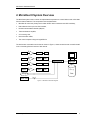
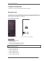
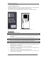
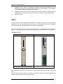
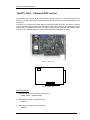
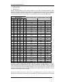
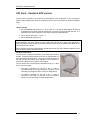
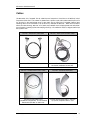
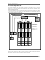
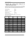
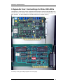
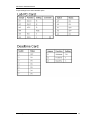
MicroDas III Hardware Manual
MicroDas
Data Acquisition
System
Microdas III Hardware Manual
Microanalyical Research Centre
School of Physics
University of Melbourne
Victoria, 3010
AUSTRALIA
Fax: + 61 (0)3 9347 4783
Ph: + 61 (0)3 8344 5376
Email: [email protected]
Web: http://www.ph.unimelb.edu.au/marco
August 2006
Microanalytical Research Centre
1
MicroDas III Hardware Manual
Preface
This document is produced as a guide for users and installers of MicroDas III. MicroDas III is
a high speed, mission critical data acquisition system for use with a nuclear microprobe in a
scientific environment.
For further technical assistance please contact MARC via the following email address:
[email protected]
Limitation of Liability
Micro Analytical Research Centre does not assume any liability arising out of the use of
the information contained within this manual. This document may contain or reference
information and products protected by copyrights or patents and does not convey any
license under the patent rights of Micro Analytical Research Centre, nor the rights of
others.
Micro Analytical Research Centre will not be liable for any defect in hardware or
software or loss or inadequacy of data of any kind, or for any direct, indirect, incidental,
or consequential damages in connections with or arising out of the performance or use
of any of its products. The foregoing limitation of liability shall be equally applicable to
any service provided by Micro Analytical Research Centre.
Note
No part of this publication may be reproduced, stored in a retrieval system, or
transmitted, in any form or by any means, electronic, mechanical, photocopying or
otherwise, without the prior written permission of MARC.
Manual Release:
Document ID:
Microanalytical Research Centre
1.7
NIM Hardware
2
MicroDas III Hardware Manual
Table of Contents
1.
INTRODUCTION ..........................................................................................................................4
2.
MICRODAS III SYSTEM OVERVIEW .....................................................................................5
3.
SYSTEM COMPONENTS ............................................................................................................6
MICRODAS III UNIT. .............................................................................................................................6
Front of MicroDas III Unit. .............................................................................................................6
ADC’S ..................................................................................................................................................8
Canberra 8701 .................................................................................................................................8
Internal Jumper settings for the Canberra 8701 module. ................................................................9
LABPC+ CARD – CANBERRA ADC VERSION .......................................................................................10
CIO CARD – CANBERRA ADC VERSION ..............................................................................................13
CABLES ...............................................................................................................................................14
4.
CONNECTING DEVICES..........................................................................................................15
5.
APPENDIX ONE: GLOSSARY .................................................................................................16
6. APPENDIX TWO: INTERNAL JUMPER SETTINGS FOR THE CANBERRA 8075 ADC
MODULE..............................................................................................................................................17
8075 Interface Adaptor ..................................................................................................................17
7.
APPENDIX THREE: CIO CABLE WIRING..........................................................................18
8.
APPENDIX FOUR: CARD SETTINGS FOR ORTEC 800 ADCS.........................................19
Microanalytical Research Centre
3
MicroDas III Hardware Manual
1. Introduction
MicroDas III is the triple width NIM module release of the original MicroDas data acquisition system and
replaces the MicroDas II which was a 19” rack mounted unit.
MicroDas was developed to offer the speed, versatility and relability required by a nuclear microprobe
data acquisition system. MicroDas III improves on predecessors by using smaller and more tightly
integrated electronics offering a higher level of reliabilty. MicroDas III is the result of over a decade of
development in the MARC laboratories.
MicroDas III offers the following capabilities:
•
Highly integrated electronics,
•
Data acquisition from up to 4 detectors simultaneously,
•
Digital scanning system,
•
Event-by-event data collection with each detector event tagged by the scan position,
•
Robust data collection for count rates well above 20kHz,
•
Deadtime corrected scanning with single detector operation,
•
Simultaneous, full deadtime correction on all four detectors is available as an option,
•
Energy spectra up to 8k channels,
•
Image maps up to 4k × 4k pixels,
•
Remote operation and monitoring of the MicroDas system.
MicroDas developed commenced by Glenn Moloney with assistance of the MARC group in 1996
This document is produced as a guide for users and installers of MicroDas III. Please see the MPSYS
User Manual and the MPSYS Installation and Administration Manual for installation and use of
software.
This document is broken up into logical sections starting with system requirements and continuing to
post-install support, maintenance and usage.
It is assumed that the hardware accessories such as cables associated with MicroDas are all present
and the computer controlling the system has been properly configured to run MPSYS 4 and drive the
MicroDas Unit, as specified in the MPSYS Installation and Administration Manual.
Triple-width MicroDas NIM module power consumption:
+/-6 V
180 mA
+/-24 V
30 mA
Note 1: The 6V rails are wired in all NIM bins, but not necessarily powered. Newer, high specification
crates, such as the “Black Max” crates provide the 6 V rails. On a lower specifications NIM crate, the
6V rails can be provided by a singe width NIM “plug-in” module.
Note 2: Post February 2004 MicroDas II modules incorporate an intenal 6 V supply and do not need the
6V rail from the NIM crate.
Cautions:
(1) Make sure power switch on MicroDas module is off before connecting the 50-way plug!
(2) Make sure power to NIM crate is off before inserting and connecting the ADC modules.
Microanalytical Research Centre
4
MicroDas III Hardware Manual
2. MicroDas III System Overview
The MicroDas system uses a number of sophisticated components to controll devices and collect data
from the detector stations: The components used are listed below:
•
MicroDas III control unit (factory set for either ORTEC 500 or Canberra 8701 ADC modules),
•
Data collection from up to four ADC modules,
•
Nuclear Instrumentation Module (NIM) bin,
•
Transconductance amplifier,
•
X-Y scanning coils,
•
Interconnection cables,
•
The control computer using running MPSYS 4.
The devices are connected to each other as shown in Figure 1, these connections are covered in detail
in the “Connecting Devices” section of this manual.
detector
detector
E1.
E2
amplifier
ADC
amplifier
ADC
MicroDas unit
detector
E1.
amplifier
ADC
detector
E1.
amplifier
ADC
E, x, y
Disk
charge
Scan coils
MpSys
(x, y)
Figure 1 – MicroDas Connection Diagram.
Microanalytical Research Centre
5
MicroDas III Hardware Manual
3. System Components
In this section, the components of the MicroDas III system are described.
MicroDas III Unit.
The MicroDas III unit is a triple width NIM module. The unit has all connectors located at the back, with
only the power switch, scan gain controls and status lights on the front panel. See figures 2 and 3 for
the front and back of the MicroDas III unit, respectively.
Front of MicroDas III Unit.
ENABLE
1
2
3
4
DATA
Power
Figure 2 – Front of MicroDas III Unit
X
Y
Figure 3 – Front of MicroDas III Unit Block Diagram
Item Description:
Listed from lower left to upper right.
1. Mains Power Switch
2. Horizontal (X) scan amplitude gain control (0-10)
3. Vertical (Y) scan amplitude gain control (0-10)
Caution: If using the MA-890 Transconductance amplifier and the MARC scanning coils these
setting should not go above 3.
4. Station 1 Enable status LED.
5. Station 2 Enable status LED.
6. Station 3 Enable status LED.
7. Station 4 Enable status LED.
8. Station 1 Data/Busy status LED.
9. Station 2 Data/Busy status LED.
Microanalytical Research Centre
6
MicroDas III Hardware Manual
10. Station 3 Data/Busy status LED.
11. Station 4 Data/Busy status LED.
Note that the Enable LEDs are not used in the present release of MicroDas. In a future release they
will indicate stations that have been diabled or enabled under software control.
The Busy LEDs indicate the approximate data rate in each station. Inactive stations will be dark.
Back of MicroDas Unit.
1
2
3
4
1
5
6
7
10
13
8
9
11
12
14
15
Figure 4 – Back of MicroDas III Unit.
Figure 5 – Block diagram of back of MicroDas III unit
Item Description:
Items required for operation are boxed.
1, 2, 3, 4
Sockets for the 4 ADC cables for detector stations 1 to 4.
•
Up to 4 ADC modules can be used. Note that it is recommended that unused stations be
disconnected.
•
An input that can gate off that MicroDas breifly to allow an external event to occor.
5
Socket for ribon cable to the LabPC+ card in computer
•
This is the main communications channel to the data acquistion system computer.
6, 10
Analog output signals to the x- and y-inputs o fthe scan amplifier.
7
Beam Blank output. A logic level intended to gate off the beam during times when the
MicroDas unit is busy processing data.
8
Charge digitiser input. Used for “dwell on charge” in full deadtime mode.
9
External output. A Logic level output that is high when data collection is in progress, this can
be used to control an external device.
11
Event counter input. Used for “dwell on events” in full deadtime mode.
12
External enable. A logic level output that is high when data collection is in progress, this can
be used to control an external device.
Microanalytical Research Centre
7
MicroDas III Hardware Manual
13
Inhibit/Busy inputs. Used to insert additional deadtime into the MicroDas deadtime counters
provided by busy signals on the spectroscopy amplifiers from each station. To be enabled in
future releases of MicroDas (Requires special cable.)
14
Deadtime correction port, (25 pin). Used when producing fully deadtime corrected images for
all four stations. Connects to the CIO card in the control computer. Special cable required.
15
NIM power socket.
ADC’s
Two types of ADC’s are be used with the MicroDas III unit, Canberra or Ortec units. The MicroDas III is
hardwired to work with either of these two at the factory. It is not possible for the unit be modified or
configured operate with a different ADC to the one which it is hardwired for.
Up to four ADC modules may be connected to the MicroDas unit. These should be set to “gated input”
mode. The conversion gain may be set up to 8k, although 1k is usually adequate for most purposes
Canberra 8701
Canberra ADC – Front
Canberra ADC - Rear
The switches are shown at default settings.
ADC modules which emulate the Canberra 8701s may also work with suitable configured MiroDas III
units.
The older Canberra ADC model 8075 may also be used with a special interface (see appendix two).
However, some dead time functions may not operate.
Microanalytical Research Centre
8
MicroDas III Hardware Manual
Internal Jumper settings for the Canberra 8701 module.
J1: Enable convertor signal:
ENC (positive) position, non-factory default
J2: Early/Late coincidence:
LATE position, factory default
J3: Polarity composite dead time output:
POS position, non-factory default
J4: Polarity dead time:
DT* (negative) position, factory default
J5: PUR connector:
LG position, factory default
J6: Overlap mode:
OVLP position, factory default
J7: relationship between pin 12 and 10 of microdas connection:
A position, factory default
J8: Dead Time signal generation mode:
A position, factory default
The rear BNC deadtime socket should be fitted with a 50 Ohm teminator.
Microanalytical Research Centre
9
MicroDas III Hardware Manual
LabPC+ Card – Canberra ADC version
The MicroDas unit connects to the data acquisition system computer via two internal cards in the
computer. The first is the LabPC card described here and the second is the CIO card described in the
next section.
The Lab-PC+ is a multifunction analog, digital, and timing I/O board for the PC. The Lab-PC+ contains
a 12-bit successive-approximation ADC with eight analog inputs, which can be configured as eight
single-ended or four differential channels. The Lab-PC+ also has two12-bit DACs with voltage outputs,
24 lines of TTL-compatible digital I/O, and six 16-bitcounter/timer channels for timing I/O.
Figure 5 – LabPC+ Card
1
5
3
2
4
Figure 6 – LabPC+ Card
Item Description:
1. Base Address selection dip switches. (Dip block A)
•
Default (10011 -> address 0x260).
2. IRQ selection jumpers. (Jumper block W5)
•
Default 5.
3. DMA selection jumpers. (Jumper block W6)
•
Default 3.
Microanalytical Research Centre
10
MicroDas III Hardware Manual
4. ISA Bus interface.
5. Data Cable port.
Although the Base Address is set to default of 0x260 it can be varied. The table indicates the switch
settings for valid base addresses for the LabPC+ card. Changing the settings on the card is not the only
step involved though. The kernel modules must be changed to reflect this. Please see the installation
and administration manual for further detail. The same applies to both the DMA and IRQ settings.
Switch Settings
Base I/O Address (Hex) I/O Address Space Used (hex)
A9
A8
A7
A6
A5
0
1
0
0
0
100
100
11F
0
1
0
0
1
120
120
13F
0
1
0
1
0
140
140
15F
0
1
0
1
1
160
160
17F
0
1
1
0
0
180
180
19F
0
1
1
0
1
1A0
1A0
1BF
0
1
1
1
0
1C0
1C0
1DF
0
1
1
1
1
001
001
1FF
1
0
0
0
0
200
200
21F
1
0
0
0
1
220
220
23F
1
0
0
1
0
240
240
25F
1
0
0
1
1
260
260
27F
1
0
1
0
0
280
280
29F
1
0
1
0
1
2A0
2A0
2BF
1
0
1
1
0
2C0
2C0
2DF
1
0
1
1
1
002
002
2FF
1
1
0
0
0
300
300
31F
1
1
0
0
1
320
320
33F
1
1
0
1
0
340
340
35F
1
1
0
1
1
360
360
37F
1
1
1
0
0
380
380
39F
1
1
1
0
1
3A0
3A0
3BF
1
1
1
1
0
3C0
3C0
3DF
1
1
1
1
1
003
003
3FF
The Lab-PC+ uses the DMA channel selected by jumpers on jumper block W6 (Item 3). The Lab-PC+
is set at the factory to use DMA Channel 3. The Lab-PC+ hardware can use DMA Channels 1, 2, and 3.
Notice that these are the three 8-bit channels on the PC I/O channel. The Lab-PC+ does not use and
cannot be configured to use the 16-bit DMA channels on the PC AT I/O channel. Two jumpers must be
installed to select a DMA channel. The DMA Acknowledge and DMA Request lines selected must have
the same number suffix for proper operation.
The Lab-PC+ board can connect to any one of the six interrupt lines of the PC I/O channel. The
interrupt line is selected by a jumper on one of the double rows of pins located above the I/O slot edge
Microanalytical Research Centre
11
MicroDas III Hardware Manual
connector (Jumper block W5, Item 2) on the Lab-PC+. To use the interrupt capability of the Lab-PC+,
you must select an interrupt line and place the jumper in the appropriate position to enable that
particular interrupt line.
Microanalytical Research Centre
12
MicroDas III Hardware Manual
CIO Card – Canberra ADC version
The CIO card is a digital i/o card used for the full deadtime mode of MicroDas. It has a number of
internal jumper settings which must be configured as shown here for the system to recognise deadtime
mode.
Jumper settings:
1. Set the ADDRESS dip switches to: 1- off, the rest on. This sets the base address to 200 and
all addresses in the range 200-203 and 204-207 are used to communicate with the card. It is
important that no other controllers on the mother board use these addresses.
2. Set the IRO jumpers: back – 7; front – 7.
3. Set the Wait state jumpers to off.
NOTE: It may be necessary to check the BIOS of the host computer to ensure no other controllers use
a base address in the range 200-207 that may conflict with the CIO card. Some types of BIOS preassign this address range to a games controller interface and this must be disabled in the BIOS for the
CIO card to function properly.
Some computers have been supplied with a special device driver that uses a different address to avoid
conflicts with the games controller interface.
Hardware connections:
The CIO card is connected to MicroDas via its internal and external
sockets. So that the internal socket can be use, an internal break-out
cable is employed as shown here. The large D connector plugs into
the CIO card and the external panel with the small D connector is
mounted in a spare slot on the back of the computer.
The CIO card is then connected to the MicroDas unit by a “Y” cable
shown on the next page.
•
The large D connector on the end of the “Y” cable is
connected directly to the large external D-connector on the
card itself (on the right end of the card in the image above).
•
The small D connector on the end of the “Y” cable is
connected to the break-out connector from the internal D
socket on the left end of the card (see image above).
Microanalytical Research Centre
13
MicroDas III Hardware Manual
Cables
The MicroDas unit is supplied with all cables that are required for connection to the MPSYS control
computer and the ADC’s. The cables are labeled with a product code, that inticates cable function, this
can be found in the approximate centre of the cable. Also on either end of supplied cables a label
indicating device to be connected to can be found. For example the MA-C02 – Dead Time Correction
cable has a label showing “MA-C02” in its centre and is labeled on the the appropriate ends “MicroDas”
and “Computer” indicating where that end/plug should go. The cables are shown in diagram below with
their product code.
MA-C01 – MicroDas to ADC Cable
MA-C02 – Dead Time Correction Cable
Connects the MicroDas unit to the ADC’s
Connects the MicroDas Deadtime output to
the control computers counter card.
MA-C03 – RG58 Interconnection Cable
MA-C04 – MicroDas Data Cable
1.1.1.1.1.1.1.1.1
Connects the MicroDas unit to
miscellaneous equipement. This is standard
RG58 cable with BNC on either end.
Microanalytical Research Centre
Connects the MicroDas LabPC+ output to
the control computers LabPC+ card
14
MicroDas III Hardware Manual
4. Connecting Devices.
The MicroDas, detectors, ADC’s and controlling computer are connected as shown in the block
diagram below. To install the hardware of the MicroDas system, follow the layout in the diagram. Italics
indicate connecting cables used.
It is recommended that the control computer, the MicroDas unit and the Scan Amplifier all be installed
in close proximity to each other, preferably in the same instrument rack to avoid problems with earth
loops and signal degradation from long cables
MA-C04 – LabPC+ Data
MA-C03 – Y Out
MA-C02 - Deadtime
MA-C03 – X Out
MicroDas
Control
Computer
MA-C01
MA-C01
MA-C01
MA-C03 – External Charge
MPSYS 4
MA-C01
A
D
C
A
D
C
A
D
C
A
D
C
Denotes Input
1
2
3
4
Denotes Output
Denotes
MA-C03
MA-C03
A
M
P
A
M
P
A
M
P
A
M
P
1
2
3
3
MA-C03
MA-C03
MA-C03
MA-C03
Scan
Coils
MA-C03
Charge
MA-C03
Scan
Amplifier
Bidirectional
DETECTOR
DETECTOR
DETECTOR
DETECTOR
STATION 1
STATION 2
STATION 3
STATION 4
Figure 7 – Connection Block Diagram.
When connecting devices ensure that all equipment is switched off and that main power has been
disconnected. The order in which devices are connected is unimportant.
Microanalytical Research Centre
15
MicroDas III Hardware Manual
5. Appendix One: Glossary
Base
Address
An address is an unsigned integer used to select one fundamental element of storage,
usually known as a word from a computer's main memory or other storage device. The
CPU outputs addresses on its address bus which may be connected to an address
decoder, cache controller, memory management unit, and other devices. While from a
hardware point of view an address is indeed an integer most strongly typed programming
languages disallow mixing integers and addresses, and indeed addresses of different
data types. This is a fine example for syntactic salt: the compiler could work without it
but makes writing bad programs more difficult. The base address of devices specifies the
first address of a range of addresses used by a device.
Bus Master
The device in a computer which is driving the address bus and bus control signals at
some point in time. In a simple architecture only the (single) CPU can be bus master but
this means that all communications between ("slave") I/O devices must involve the CPU.
More sophisticated architectures allow other capable devices (or multiple CPUs) to take
turns at controling the bus. This allows, for example, a network controller card to access
a disk controller directly while the CPU performs other tasks which do not require the
bus, e.g. fetching code from its cache.
DMA Direct
Memory
Access
A facility of some architectures which allows a peripheral to read and write memory
without intervention by the CPU. DMA is a limited form of bus mastering.
IRQ interrupt
request
The name of an input found on many processors which causes the processor to suspend
normal instruction execution temporarily and to start executing an interrupt handler
routine. Such an input may be either "level sensitive" - the interrupt condition will persist
as long as the input is active or "edge triggered" – an interrupt is signalled by a low-tohigh or high-to-low transition on the input. Some processors have several interrupt
request inputs allowing different priority interrupts.
Kernel
The essential part of Unix or other operating systems, responsible for resource
allocation, low-level hardware interfaces, security etc.
Microanalytical Research Centre
16
MicroDas III Hardware Manual
6. Appendix Two: Internal jumper settings for the
Canberra 8075 ADC module.
The Canberra 8075 ADC module predates the 8701 module but can also be used with MicroDas
provided the internal jumper settings are set as follows and an adaptor cable is made as described in
the table below. However it is recommended that MicroDas be used only with 8701 ADC modules.
There is no guarantee that all functions of MicroDas will be available with 8075 ADC modules.
J6: Enable data signal:
NEG true
J7: Data accepted signal:
NEG true
J8: Data ready:
NEG true
J9: Dead time connector function:
INput
J10: Dead time output:
POS true
J11: Early/Late coincidence:
LATE position
R145: dead time signal generation mode
BC
Note: All dead time functions may not be operational on these older ADC models!
8075 Interface Adaptor
MPSYS (34pin)
Description
ADC 8075
(26pin)
Signal Type
(@ADC)
1
2
3
4
5
6
7
8
9
10
11
12
13
GND
ACCEPT
GND
ENB DATA
GND
CDT
GND
ENB CONV
GND
DATA READY
GND
INB (INV)
not used
(reserved)
DATA 0
DATA 7
DATA 1
DATA 8
DATA 2
DATA 9
DATA 3
DATA 10
DATA 4
DATA 11
DATA 5
DATA 12
DATA 6
not used by
MPSYS
22
8
22
18
22
16
22
10
22
2
22
14
GND
Input
GND
Input
GND
Output
GND
Input
GND
Output
GND
Output
1
15
3
17
5
19
7
21
9
23
11
25
13
4,6,12,20,24,26
Output
Output
Output
Output
Output
Output
Output
Output
Output
Output
Output
Output
Output
14
15
16
17
18
19
20
21
22
23
24
25
26
27-34
Microanalytical Research Centre
Logic (see
Jumper
settings!)
NEG true
NEG true
POS true
POS true
NEG true
17
MicroDas III Hardware Manual
7. Appendix Three: CIO cable wiring
The configuration of the internal and external cables used to connect the CIO card to the MicroDas unit
is shown here (revision 2 - August 2006).
Microanalytical Research Centre
18
MicroDas III Hardware Manual
8. Appendix Four: Card settings for Ortec 800 ADCs
This appendix is for the early versions of MicroDas that interfaced to the Ortec model 800 ADC units.
As these untis are now obsolete, these settings are only useful to the few early model MicroDas units
still in operation. (As used in Melbourne on the MP2 beam line and computer “praxis”.)
A summary of the jumper settings appears on the next page.
Microanalytical Research Centre
19
MicroDas III Hardware Manual
Jumper settings for the Ortec 800 ADC option.
Microanalytical Research Centre
20