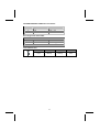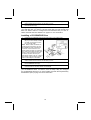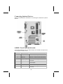
1
Preface
Copyright
This publication, including all photographs, illustrations and software, is protected under international copyright laws, with all rights reserved. Neither this manual, nor any
of the material contained herein, may be reproduced without written consent of the author.
Version 1.0
Disclaimer
The information in this document is subject to change without notice. The manufacturer makes no representations or warranties with respect to the contents hereof and
specifically disclaim any implied warranties of merchantability or fitness for any particular purpose. The manufacturer reserves the right to revise this publication and to
make changes from time to time in the content hereof without obligation of the manufacturer to notify any person of such revision or changes.
Trademark Recognition
Microsoft, MS-DOS and Windows are registered trademarks of Microsoft Corp.
MMX, Pentium, Pentium-II, Pentium-III, Celeron are registered trademarks of Intel
Corporation.
Other product names used in this manual are the properties of their respective owners
and are acknowledged.
Federal Communications Commission (FCC)
This equipment has been tested and found to comply with the limits for a Class B digital device, pursuant to Part 15 of the FCC Rules. These limits are designed to provide
reasonable protection against harmful interference in a residential installation. This
equipment generates, uses, and can radiate radio frequency energy and, if not installed and used in accordance with the instructions, may cause harmful interference
to radio communications. However, there is no guarantee that interference will not occur in a particular installation. If this equipment does cause harmful interference to
radio or television reception, which can be determined by turning the equipment off
and on, the user is encouraged to try to correct the interference by one or more of the
following measures:
−
−
−
−
Reorient or relocate the receiving antenna.
Increase the separation between the equipment and the receiver.
Connect the equipment onto an outlet on a circuit different from that to which
the receiver is connected.
Consult the dealer or an experienced radio/TV technician for help.
Copyright © 2002
All Rights Reserved
MS9127C, V1.0
VT8754/August 2002
i
Shielded interconnect cables and a shielded AC power cable must be employed with
this equipment to ensure compliance with the pertinent RF emission limits governing
this device. Changes or modifications not expressly approved by the system's manufacturer could void the user's authority to operate the equipment.
Declaration of Conformity
This device complies with part 15 of the FCC rules. Operation is subject to the following conditions:
−
−
This device may not cause harmful interference, and
This device must accept any interference received, including interference
that may cause undesired operation.
Canadian Department of Communications
This class B digital apparatus meets all requirements of the Canadian Interferencecausing Equipment Regulations.
Cet appareil numérique de la classe B respecte toutes les exigences du Réglement
sur le matériel brouilieur du Canada.
About the Manual
The manual consists of the following:
Chapter 1
Describes features of the mainboard,
and provides a shipping checklist.
Introducing the Mainboard
Go to ⇒ page 3
Chapter 2
Describes installation of mainboard
components.
Installing the Mainboard
Go to ⇒ page 3
Chapter 3
Provides information on using the BIOS
Setup Utility.
Using BIOS
Go to ⇒ page 3
Chapter 4
Describes the mainboard software.
Using the Mainboard Software
Go to ⇒ page 3
ii
TABLE OF CONTENTS
Preface
i
CHAPTER 1
3
Introducing the Mainboard
3
Introduction .................................................................................................3
Checklist .....................................................................................................3
Standard Items ................................................................................................. 3
Features .....................................................................................................3
Choosing a Computer Case .......................................................................3
Mainboard Components .............................................................................3
CHAPTER 2
3
Installing the Mainboard
3
Safety Precautions......................................................................................3
Quick Guide ................................................................................................3
Installing the Mainboard in a Case..............................................................3
Checking Jumper Settings ..........................................................................3
Setting Jumpers ............................................................................................... 3
Checking Jumper Settings ............................................................................... 3
Jumper Settings ............................................................................................... 3
Connecting Case Components ...................................................................3
Front Panel Connector ..................................................................................... 3
Installing Hardware .....................................................................................3
Installing the Processor.................................................................................... 3
Installing Memory Modules ............................................................................ 3
Installing a Hard Disk Drive/CD-ROM........................................................... 3
Installing a Floppy Diskette Drive................................................................. 20
Installing Add-on Cards................................................................................... 3
Connecting Optional Devices .......................................................................... 3
Connecting I/O Devices ..............................................................................3
External Connector Color Coding ................................................................... 3
CHAPTER 3
3
Using BIOS
3
About the Setup Utility ................................................................................3
The Standard Configuration ............................................................................ 3
Entering the Setup Utility ................................................................................ 3
Updating the BIOS .......................................................................................... 3
Using BIOS .................................................................................................3
Standard CMOS Features .............................................................................. 30
Advanced BIOS Features ................................................................................ 3
Advanced Chipset Features ............................................................................. 3
iii
Integrated Peripherals ...................................................................................... 3
Power Management Setup ............................................................................... 3
PNP/PCI Configurations.................................................................................. 3
PC Health Status.............................................................................................. 3
Frequency/Voltage Control.............................................................................. 3
Load Fail-Safe Defaults................................................................................. 50
Load Optimized Defaults............................................................................... 50
Set Supervisor/User Password......................................................................... 3
Save & Exit Setup ........................................................................................... 3
Exit Without Saving ........................................................................................ 3
錯誤! 尚未定義書籤。
CHAPTER 4
錯誤! 尚未定義書籤。
Using the Mainboard Software
About the Software CD-ROM .................................... 錯誤! 尚未定義書籤。
Utility Software Reference ......................................... 錯誤! 尚未定義書籤。
iv
Chapter 1
Introducing the Mainboard
Introduction
Thank you for purchasing the MS9127C mainboard. The MS9127C is designed to accommodate Intel Pentium 4 processors supporting front side bus
(FSB) speeds of 400/533 MHz.
The mainboard is an ATX mainboard that uses a 4-layers printed circuit board
and measures 305 mm x 190 mm.
Based on the highly integrated VIA APOLLO P4X400, this mainboard incorporates the VIA VT8754 Northbridge and VT8235 Southbridge chipsets which
delivers workstation level performance.
The MS9127C comes with a full set of I/O features conveniently integrated on
the rear I/O panel, including support for PS/2 keyboard and mouse connectors,
Six USB ports (Four back-panel USB 2.0 ports, onboard USB headers providing maximum two extra ports) , a LAN connector, two high-speed serial port,
an EPP/ECP parallel port, audio jacks for microphone, line-in, line-out and
CD-in, as well as supporting Plug and Play.
For added power and performance, the mainboard achieves the highest reliability by supporting three 184 pin, 2.5V DDR (Double Data RAM) DIMM
sockets with a total capacity of 3 GB.
The MS9127C offers the ideal platform for building powerful PCs and workstations.
Note: SDRAM provides 800 MBps or 1 GBps data transfer depending on
whether the bus is 100MHz or 133MHz. Double Data Rate SDRAM
(DDR SDRAM) doubles the rate to 1.6 GBps and 2.7 GBps. DDR
SDRAM uses additional power and ground lines and requires 184-pin
DIMM modules rather than the 168-pin DIMMs used by SDRAM.
Checklist
Compare the mainboard’s package contents with the following checklist:
Standard Items
•
•
•
•
•
•
•
One mainboard
One diskette drive ribbon cable
One IDE drive ribbon cable
One auto-install software support CD
One I/O panel
One retention module
This user’s manual
1
Features
Processor
Chipset
Memory
AGP
The MS9127C mainboard includes a mPGA Socket 478 that
has the following features:
•
Supports up to a 400/533 MHz front side bus (FSB)
•
Accommodates Intel Pentium 4 processors
The chipset on MS9127C includes the VT8754 Northbridge
and VT8235 Southbridge which are based on an innovative
and scalable architecture with proven reliability and performance. A few of the chipset’s advanced features are:
•
An advanced V-Link memory controller architecture that
provides the 512 MB/s bandwidth and performance necessary for even the most demanding Internet and 3D
graphics
•
Support for an 2x/4x/8xAGP interface providing vivid 3D
graphics and video performance
•
An ATA 133 interface on the VT8235 chipset, which helps
boost system performance by providing a high-speed
connection to ATA 133 Hard Disk Drives, delivering
maximum sustained data transfer rates of 133 MB/sec
Additional features include support for Six USB ports (Four
back-panel USB 2.0 ports, onboard USB headers providing
maximum two extra ports), an AC 97 link for audio and modem, hardware monitoring, and ACPI/OnNow power
management.
•
Supports DDR SDRAM up to 200/266/333 MHz memory
module
•
Accommodates three 184 pin, 2.5V DDR DIMM sockets
with a total capacity of 3 GB.
The MS9127C includes an 8xAGP slot that provides eight
times the bandwidth of the original AGP specification. The
AGP 3.0 (8xAGP) offers a significant increase in performance
along with feature enhancements to AGP2.0. This interface
represents the natural evolution from the existing AGP to meet
the ever-increasing demands placed on the graphic interfaces
within the workstation and desktop environments.
AC’ 97 Audio
Codec
The AC’97 Audio codec is compliant with the AC’ 97 2.2 specification, and supports 18-bit ADC (Analog Digital Converter)
and DAC (Digital Analog Converter) resolution as well as 18-bit
stereo full-duplex codec with independent and variable sampling rates. Further features include support for four analog
line-level stereo inputs.
USB 2.0
The built-in VIA VT8235 PCI USB 2.0 Controller is compliant
with Universal Serial Bus Specification Revision 2.0.
The USB 2.0 supports data transfer rates up to 480Mb/sec for
high-speed devices and specifies a microframe that will be
th
1/8 of a 1msec frame. This allows the USB 2.0 devices to
have small buffers even at high data rates.
The USB 1.1 connectors and other full speed cables can support the higher speed of USB 2.0 without any changes.
2
Expansion
Options
10/100 LAN
(optional)
Integrated I/O
BIOS
Firmware
The chipset has the following advanced USB features:
•
Compliant with Enhanced Host Controller Interface
(EHCI) Specification Revision 0.95 and Universal Host
Controller Interface (UHCI) Specification Revision 1.1
•
PCI multi-function device consists of two UHCI Host Controllers for full/low-speed signaling and one EHCI Host
Controller core for high-speed signaling
•
Supports PCI-Bus Power Management Interface Specification release 1.1
•
Legacy support for all downstream facing ports
The mainboard comes with the following expansion options:
•
Five 32-bit PCI slots
•
One 8xAGP slot
•
A Communications Network Riser (CNR) slot (AC97 interface only)
•
Two IDE connectors which support four IDE channels and
a floppy disk drive interface
The MS9127C is capable of Ultra DMA bus mastering with
transfer rates of 33/66/100/133 MB/sec.
The VT6103 is a Physical Layer device for Ethernet 10BASE-T
and 100BASE-TX using category 5 Unshielded, Type 1
Shielded, and Fiber Optic cables.
•
Dual Speed – 100/10 Mbps
•
Half And Full Duplex
•
Meet All Applicable IEEE 802.3, 10Base-T and 100BaseTx Standards
•
Adaptive Equalizer
The mainboard has a full set of I/O ports and connectors:
•
Two PS/2 ports for mouse and keyboard
•
Two serial port
•
One parallel port
•
Six USB ports (Four backpanel ports, onboard USB
headers providing two extra ports)
•
Audio jacks for microphone, line-in and line-out
This mainboard uses Award BIOS that enables users to configure many system features including the following:
•
Power management
•
CPU and memory timing
•
Modem wake up alarms
The firmware can also be used to set parameters for different
processor clock speeds.
3
Choosing a Computer Case
There are many types of computer cases on the market. The mainboard complies with the specifications for the ATX system case. Some features on the
mainboard are implemented by cabling connectors on the mainboard to indicators and switches on the system case. Ensure that your case supports all
the features required. The mainboard can support one floppy diskette drive
and four enhanced IDE drives. Ensure that your case has sufficient power and
space for all the drives that you intend to install.
Most cases have a choice of I/O templates in the rear panel. Make sure that
the I/O template in the case matches the I/O ports installed on the rear edge
of the mainboard.
This mainboard has an ATX form factor of 305 x 190 mm. Choose a case that
accommodates this form factor.
4
Mainboard Components
5
Table of Mainboard Components
Label
AGP1
ATX1
ATX2
AUDIO1
BT1
CASFAN1
CD1
CD2
CNR1
CPU SOCKET
CPUFAN1
DDR1 ~ DDR3
FDD1
IDE 1
IDE 2
JP1
JP2
LED1 (optional S3)
PANEL1
PCI1 ~ PCI5
SJ1
SIR1
SMI1
SPDIFO1
USB3
Component
Accelerated Graphics Port
Standard 20-pin ATX power connector
Power connector
Mic/speaker-out connector
Three volt realtime clock battery
Auxiliary case cooling fan
Primary CD-in connector (Sony)
Secondary CD-in connector (Panasonic)
Communications Networking Riser slot
CPU Socket (mPGA478)
Cooling fan for CPU
Three 184-pin DDR DIMM sockets
Floppy disk drive connector
Primary IDE channel
Secondary IDE channel
Clear CMOS jumper
CPU bus speed select jumper
LED 2.5 VSB for DDR SDRAM (red)
Panel connector for case switches and LEDs
Five 32-bit add-on card slots
Single-color LED header
Serial infrared port
External System Management Interrupt header
SPDIF out header
Connector for front panel USB ports
Note: LED1 is usually connected to a light that indicates that the computer is
powered on. Do not install hardware or disconnect power cables while the
LED is on.
This concludes Chapter 1. The next chapter explains how to install the mainboard.
6
Chapter 2
Installing the Mainboard
Safety Precautions
Follow these safety precautions when installing the mainboard:
•
•
•
•
Wear a grounding strap attached to a grounded device to avoid
damage from static electricity.
Discharge static electricity by touching the metal case of a safely
grounded object before working on the mainboard.
Leave components in the static-proof bags they came in.
Hold all circuit boards by the edges. Do not bend circuit boards.
Quick Guide
This Quick Guide suggests the steps you can take to assemble your system
with the mainboards.
The following table provides a reference for installing specific components:
Locating Mainboard Components
Go to page 3
Installing the Mainboard in a Case
Go to page 3
Setting Jumpers
Go to page 3
Installing Case Components
Go to page 3
Installing the CPU
Go to page 3
Installing Memory
Go to page 3
Installing a HDD and CD-ROM Drive
Go to page 3
Installing a FDD
Go to page 20
Installing Add-on Cards
Go to page 3
Connecting Options
Go to page 3
Connecting Peripheral (I/O) Devices
Go to page 26
7
Installing the Mainboard in a Case
Refer to the following illustration and instructions for installing the mainboard
in a case:
This illustration shows an example of a mainboard being
installed in a tower-type case:
Note:
2. Secure the mainboard with
screws where appropriate.
Do not overtighten
the screws as this
can stress the mainboard.
Most system cases have
mounting brackets installed in
the case, which correspond to
the holes in the mainboard.
Place the mainboard over the
mounting brackets and secure
the mainboard onto the mounting brackets with screws.
1. Place the mainboard
over the mounting brackets.
Ensure that your case has an I/O template that supports the I/O ports and
expansion slots on your mainboard.
Checking Jumper Settings
This section explains how to set jumpers for correct configuration of the mainboard.
Setting Jumpers
Use the mainboard jumpers to set system configuration options. Jumpers with
more than one pin are numbered. When setting the jumpers, ensure that the
jumper caps are placed on the correct pins.
The illustrations below show a 2-pin jumper.
When the jumper cap is placed on both pins,
the jumper is SHORT. If you remove the
jumper cap, or place the jumper cap on just
one pin, the jumper is OPEN.
Short
This illustration shows a 3-pin
jumper. Pins 1 and 2 are SHORT.
1 2
3
Open
8
Checking Jumper Settings
The following illustration shows the location of the mainboard jumpers. Pin 1 is
labeled.
Jumper Settings
Jumper
Type
JP1
3 pin
Description
Setting (default)
Clear CMOS
jumper
1-2: Normal
JP1
2-3: Clear CMOS
1
JP2
3 pin
CPU bus speed
select jumper
1-2: Auto
JP2
2-3: 533 MHz
1
JP1 - This jumper enables you to reset BIOS. Follow these instructions:
1.
2.
3.
4.
Turn the system off.
Short pins 2 and 3 on JP1.
Return the jumper to the normal setting.
Turn the system on. The BIOS is returned to the default settings.
JP2 - This jumper enables to set the CPU frequency.
9
Connecting Case Components
After you have installed the mainboard into a case, you can begin connecting
the mainboard components. Refer to the following:
1.
2.
3.
4.
5.
6.
Connect the Pentium
4 processor auxiliary
case power supply
connector to ATX2.
Connect the standard
power supply connector to ATX1.
Connect the CPU
cooling fan cable to
CPUFAN1.
Connect the case
cooling fan connector
to CASFAN1.
Connect the case
switches and indicator
to PANEL1.
Connect the case
LED cable to SJ1.
Note: When the system is heavily loaded, you should install, at a minimum,
an ATX12V power supply with a 300W capacity.
ATX1: ATX 20-pin Power Connector
Pin
Signal Name
Pin
Signal Name
1
2
3
4
5
6
7
8
9
10
+3.3V
+3.3V
Ground
+5V
Ground
+5V
Ground
PWRGD
+5VSB
+12V
11
12
13
14
15
16
17
18
19
20
+3.3V
-12V
Ground
PS ON#
Ground
Ground
Ground
+5V
+5V
+5V
TX2: ATX 12V Power Connector
Pin
1
2
3
4
Signal Name
+12V
+12V
Ground
Ground
10
CPUFAN1/CASFAN1: FAN Power Connectors
Pin
1
2
3
Signal Name
Function
GND
+12V
Sense
System Ground
Power +12V
Sensor
SJ1: Single color LED header
Pin
1
2
3
Signal Name
Function
ACPI LED
ACPI LED
SB5V
MSG LED (-) green
MSG LED (-) green
Power LED (+)
ACPI LED function:
SJ1
1
S0
S1
S3
S4/S5
Light
Blinking
Blinking
Dark
11
Front Panel Connector
The front panel connector (PANEL1) provides a standard set of switch and
LED connectors commonly found on ATX or micro-ATX cases. Refer to the
table below for information:
Pin
Signal Name
Function
1
HD_LED_P
Hard disk LED pull up (330 ohm) to +5V
2
FP PWR/SLP
MSG LED pull up (330 ohm) to +5V
3
PANEL1
HD_LED_N
Hard disk active LED
4
GND
Ground
5
RST_SW_N
Reset Switch low reference pull down (100 ohm) to GND
6
PWR_SW_P
Power Switch high reference pull up (10000 ohm) to +5V
7
RST_SW_P
Reset Switch high reference pull up (1000 ohm) to +5V
8
PWR_SW_N
Power Switch high reference pull down (100 ohm) to GND
9
RSVD
12
Reserved (do not use)
10
NC
No pin
Hard Drive Activity LED
Connecting pins 1 and 3 to a front panel mounted LED provides visual indication that data is being read from or written to the hard drive. For the LED to
function properly, an IDE drive should be connected to the onboard IDE interface. The LED will also show activity for devices connected to the SCSI (hard
drive activity LED) connector.
Power / Sleep / Message Waiting LED
Connecting pins 2 and 4 to a single- or dual-color, front panel mounted LED
provides power on/off, sleep, and message waiting indication.
Reset Switch
Supporting the reset function requires connecting pins 5 and 7 to a momentary-contact switch that is normally open. When the switch is closed, the board
resets and runs POST.
Power Switch
Supporting the power on/off function requires connecting pins 6 and 8 to a
momentary-contact switch that is normally open. The switch should maintain
contact for at least 50 ms to signal the power supply to switch on or off. The
time requirement is due to internal debounce circuitry. After receiving a power
on/off signal, at least two seconds elapses before the power supply recognizes another on/off signal.
Installing Hardware
Installing the Processor
Caution: When installing a CPU heatsink and cooling fan make sure that
you DO NOT scratch the mainboard or any of the surface-mount resistors
with the clip of the cooling fan. If the clip of the cooling fan scrapes across the mainboard, you may cause serious damage to the mainboard or
its components.
On most mainboards, there are small surface-mount resistors near the
processor socket, which may be damaged if the cooling fan is carelessly
installed.
13
Avoid using cooling fans with sharp edges on the fan casing and the
clips. Also, install the cooling fan in a well-lit work area so that you can
clearly see the mainboard and processor socket.
Before installing the Processor
This mainboard automatically determines the CPU clock frequency and system bus frequency for the processor. You may be able to change these
settings by making changes to jumpers on the mainboard, or changing the
settings in the system Setup Utility. We strongly recommend that you do not
overclock processors or other components to run faster than their rated speed.
Warning: Overclocking components can adversely affect the reliability of
the system and introduce errors into your system. Overclocking can permanently damage the mainboard by generating excess heat in
components that are run beyond the rated limits.
This mainboard has a Socket 478 processor socket. When choosing a processor, consider the performance requirements of the system. Performance is
based on the processor design, the clock speed and system bus frequency of
the processor, and the quantity of internal cache memory and external cache
memory.
CPU Installation Procedure
The following illustration shows CPU installation components:
14
Note: The pin-1 corner is marked with an arrow
Follow these instructions to install the Retention Module and CPU:
1.
Remove the existing retention module (if applicable).
2.
Position the backplate
against the underside of
the mainboard; secure
the 4 screws firmly on
the retention module.
Note: Do not over tighten
the screws.
3.
Install your CPU. Pull up
the lever away from the
socket and lift up to 90degree angle.
15
4.
Locate the CPU cut
edge (the corner with the
pinhole noticeably missing). Align and insert the
CPU correctly.
5.
Press the lever down.
6.
Apply thermal grease on top of the CPU.
7.
Put the CPU Fan down
on the retention module
and snap the four retention legs of the cooling
fan into place.
8.
Flip the levers over to lock the heat sink in place.
9.
Connect the CPU Cooling Fan power cable to
the CPUFAN1 connector. This completes the
installation.
Note: CPU fan and heatsink installation procedures may vary with the type of
CPU fan/heatsink supplied. The form and size of fan/heatsink may also
vary.
16
Installing Memory Modules
This mainboard accommodates 184-pin 2.5V unbuffered Double Data Rate
(DDR) SDRAM memory modules. The memory chips must be standard or
registered SDRAM (Synchronous Dynamic Random Access Memory).
The memory bus can run at 100/133/166 MHz. If your processor operates
over a 100 MHz system bus, you can install DDR200 or DDR266/DDR333
memory modules that operate over a 100/133/166 MHz memory bus.
The mainboard accommodates three memory modules. You must install at
least one module in any of the three slots. Each module can be installed with
up to 1 GB of memory; total memory capacity is 3 GB.
Do not remove any memory module from its antistatic packaging until
you are ready to install it on the mainboard. Handle the modules only by
their edges. Do not touch the components or metal parts. Always wear
a grounding strap when you handle the modules.
Installation Procedure
Refer to the following to install the memory modules.
1.
This mainboard supports unbuffered DDR SDRAM only. Do not attempt to
insert any other type of DDR SDRAM into the slots.
2.
Push the latches on each side of the DIMM slot down.
3.
Align the memory module with
the slot. The DIMM slots are
keyed with notches and the
DIMMs are keyed with cutouts
so that they can only be installed correctly.
4.
Check that the cutouts on the
DIMM module edge connector
match the notches in the
DIMM slot.
5.
Install the DIMM module into
the slot and press it firmly
down until it seats correctly.
The slot latches are levered
upwards and latch on to the
edges of the DIMM.
6.
Install any remaining DIMM modules.
17
DDR SDRAM memory module table:
DDR 266
DDR 333
DDR 400
3 DIMMS
3 DIMMS
2 DIMMS
Note: We do not guarantee that all DDR 400 memory modules will work properly with your mainboard.
Installing a Hard Disk Drive/CD-ROM
This section describes how to install IDE devices such as a hard disk drive
and a CD-ROM drive.
About IDE1 and IDE2 Devices
Your mainboard has a primary and secondary IDE channel interface (IDE1 and
IDE2). An IDE ribbon cable supporting two IDE devices is bundled with the mainboard.
If you want to install more than two IDE devices, get a second IDE cable and
you can add two more devices to the secondary IDE channel.
IDE devices have jumpers or switches that are used to set the IDE device as
MASTER or SLAVE. Refer to the IDE device user’s manual. When installing two
IDE devices on one cable, ensure that one device is set to MASTER and the
other device is set to SLAVE. The documentation of your IDE device explains
how to do this.
About UltraDMA
This mainboard supports Ultra DMA 33/66/100/133. UDMA is a technology
that accelerates the performance of devices in the IDE1 and IDE2 channel. To
maximize performance, install IDE devices that support UDMA and use 80-pin
IDE cables that support UDMA 33/66/100/133.
Installing a Hard Disk Drive
1.
2.
Install the hard disk drive into the drive cage in your system case.
Plug the IDE cable into IDE1
(A):
Note: Ribbon cable connectors
are usually keyed so that they can
only be installed correctly on the
device connector. If the connector
is not keyed, make sure that you
match the pin-1 side of the cable
connector with the pin-1 side of the
device connector. Each connector
has the pin-1 side clearly marked.
The pin-1 side of each ribbon cable is always marked with a
colored stripe on the cable.
18
3.
4.
Plug an IDE cable connector into the hard disk drive IDE connector (B). It
doesn't matter which connector on the cable you use.
Plug a power cable from the case power supply into the power connector on
the hard disk drive (C).
When you first start up your system, the BIOS should automatically detect
your hard disk drive. If it doesn’t, enter the Setup Utility and use the IDE Hard
Disk Auto Detect feature to configure the hard disk drive that you have installed. See IDE HDD Auto-Detection on page 3 for more information.
Installing a CD-ROM/DVD Drive
1.
2.
Install the CD-ROM/DVD drive into the drive cage in your system case.
Plug the IDE cable into IDE1
(A). If you have already installed
an HDD, use the other connector on the IDE cable.
Note: Ribbon cable connectors are
usually keyed so that they can only
be installed correctly on the device
connector. If the connector is not
keyed, make sure that you match the
pin-1 side of the cable connector with
the pin-1 side of the device connector. Each connector has the pin-1
side clearly marked. The pin-1 side of
each ribbon cable is always marked
with a colored stripe on the cable.
3. Plug an IDE cable connector into the CD-ROM/DVD drive IDE connector (B). It
doesn't matter which connector on the cable you use.
4. Plug a power cable from the case power supply into the power connector on
the CD-ROM/DVD drive (C).
5. Use the audio cable provided with the CD-ROM/DVD drive to connect to the
mainboard CD-in connector CDIN1 or CDIN2 (D).
When you first start up your system, the BIOS should automatically detect
your CD-ROM/DVD drive. If it doesn’t, enter the Setup Utility and configure
the CD-ROM/DVD drive that you have installed. See IDE Primary/Secondary
Master/Slave (Auto) on page 3 for more information.
19
Installing a Floppy Diskette Drive
The mainboard has a floppy diskette drive (FDD) interface and ships with a
diskette drive ribbon cable that supports one or two floppy diskette drives. You
can install a 5.25-inch drive and a 3.5-inch drive with various capacities. The
floppy diskette drive cable has one type of connector for a 5.25-inch drive and
another type of connector for a 3.5-inch drive.
1.
2.
Install the FDD into the drive cage in your system case.
Plug the FDD cable into
FLOPPY1 (A):
Note: Ribbon cable connectors are
usually keyed so that they can only
be installed correctly on the device
connector. If the connector is not
keyed, make sure that you match the
pin-1 side of the cable connector with
the pin-1 side of the device connector. Each connector has the pin-1
side clearly marked. The pin-1 side of
each ribbon cable is always marked
with a colored stripe on the cable.
3. Plug the correct connector on the FDD cable for the 5.25-inch or 3.5-inch drive
into the FDD connector (B).
4. Plug a power cable from the case power supply into the power connector on
the FDD (C).
When you first start up your system, go immediately to the Setup Utility to
configure the floppy diskette drives that you have installed. See Standard
CMOS Features on page 3 for more information.
20
Installing Add-on Cards
This mainboard has five 32-bit PCI (Peripheral Components Interconnect)
expansion slots, one 8xAGP slot, and one Communications and Networking
Riser (CNR) slot.
PCI Slots
PCI slots are used to install expansion cards that have the 32-bit
PCI interface.
8xAGP Slot
The 8xAGP slot is used to install a graphics adapter that supports
the universal AGP 3.0 specification and has a 1.5V-keyed connector.
Note: The above layout is for reference only. The AGP slot
may be different from your mainboard. Please refer to
actual shipment.
Do not use AGP 2X card (3.3V) in this motherboard. It
will burn and damage the motherboard due to VIA
P4X400 chipset can't support AGP 2X(3.3V).
CNR Slot
This slot is used to insert CNR cards with Modem and Audio functionality.
Note: Before installing an add-on card, check the documentation for the card
carefully. If the card is not Plug and Play, you may have to manually configure the card before installation.
21
Follow these instructions to install an add-on card:
1.
2.
3.
Remove a blanking plate from the system case corresponding to the slot you
are going to use.
Install the 1.5V-keyed connector
of the add-on card into the expansion slot. Ensure that the
edge connector is correctly
seated in the slot.
Secure the metal bracket of the card to the system case with a screw.
Note: For some add-on cards, for example graphics adapters and network adapters,
you have to install drivers and software before you can begin using the add-on
card.
22
Connecting Optional Devices
Refer to the following for information on connecting the mainboard’s optional
devices:
AUDIO1: Front Panel Audio header
This header allows the user to install auxiliary front-oriented microphone and
line-out ports for easier access.
Pin
Signal Name
Function
1
2
3
4
5
6
AUD_MIC
AUD_GND
AUD_MIC_BIAS
AUD_VCC
AUD_FPOUT_R
AUD_RET_R
7
HP_ON
8
9
10
KEY
AUD_FPOUT_L
AUD_RET_L
Front Panel Microphone input signal
Ground used by Analog Audio Circuits
Microphone Power
Filtered +5 V used by Analog Audio Circuits
Right Channel Audio signal to Front Panel
Right Channel Audio signal to Return from
Front Panel
Reserved for future use to control Headphone Amplifier
No Pin
Left Channel Audio signal to Front Panel
Left Channel Audio signal Return from
Front Panel
23
USB3: Front panel USB connectors
The mainboard has two USB ports installed on the rear edge I/O port array.
Additionally, some computer cases have USB ports at the front of the case. If
you have this kind of case, use auxiliary USB connector USB3 to connect the
front-mounted ports to the mainboard.
Pin
Signal Name
Function
1
2
3
4
5
6
7
8
9
10
VREG_FP_USBPWR0
VREG_FP_USBPWR0
USB_FP_P0USB_FP_P1USB_FP_P0+
USB_FP_P1+
GND
GND
KEY
USB_FP_OC0
Front Panel USB Power
Front Panel USB Power
USB Port 0 Negative Signal
USB Port 1 Negative Signal
USB Port 0 Positive Signal
USB Port 1 Positive Signal
Ground
Ground
No pin
Overcurrent signal
Note: Please make sure that the USB cable has the same pin assignment as indicated above. A different pin assignment may cause damage or system
hang-up.
SIR1: Serial infrared port
The mainboard supports a Serial Infrared (SIR) data port. Infrared ports allow
the wireless exchange of information between your computer and similarly
equipped devices such as printers, laptops, Personal Digital Assistants
(PDAs), and other computers.
Pin
Signal Name
Function
1
2
3
4
5
6
Not assigned
KEY
+5V
GND
IRTX
IRRX
Not assigned
No pin
IR Power
Ground
IrDA serial output
IrDA serial input
SMI1: System Management Interrupt
This connector is for use with SMI hardware interrupt power management.
Pin
1
2
Signal Name
Function
-EXTSMI
GND
Sleep button
Ground
24
SPDIFO1: SPDIF out header
You can purchase an optional 24-bit digital audio extension bracket from a
third-party vendor. You can use the audio RCA jacks to connect to digital audio
devices. If your CD-ROM/DVD drive has digital audio output, you can connect
it to the input pins of the SPDIF connector.
Pin
1
2
3
4
Signal Name
Function
SPDIF
+5VA
NC
GND
SPDIF digital output
5V analog power
Not connected
Ground
25
Connecting I/O Devices
The backplane of the mainboard has the following I/O ports:
PS/2 Mouse
PS/2 Keyboard
LPT1
COM1/2
Audio Ports
LAN Port
USB Ports
Use the upper PS/2 port to connect a PS/2 pointing device.
Use the lower PS/2 port to connect a PS/2 keyboard.
Use LPT1 to connect printers or other parallel communications devices.
Use the COM ports to connect serial devices such as mice
or fax/modems. COM1 is identified by the system as
COM1/3. COM2 is identified by the system as COM2/4.
Use the three audio ports to connect audio devices. The left
side jack is for a stereo line-out signal. The middle jack is for
a stereo line-in signal. The right side jack is for a microphone.
Connect an RJ-45 jack to this port to connect your PC to the
LAN.
Use the USB ports to connect USB devices.
External Connector Color Coding
Many connectors now use standard colors as shown in the table below.
Connector
Color
Audio line-in
Audio line-out
Microphone
MIDI/game
Parallel
PS/2-compatible keyboard
PS/2-compatible mouse
Serial
USB + LAN
SCSI, network, telephone, modem
Light blue
Lime
Pink
Gold
Burgundy
Purple
Green
Teal or Turquoise
Black
None
This concludes Chapter 2. The next chapter covers the BIOS.
26
Chapter 3
Using BIOS
About the Setup Utility
The computer uses the latest Award BIOS with support for Windows Plug and
Play. The CMOS chip on the mainboard contains the ROM setup instructions
for configuring the mainboard BIOS.
The BIOS (Basic Input and Output System) Setup Utility displays the system's
configuration status and provides you with options to set system parameters.
The parameters are stored in battery-backed-up CMOS RAM that saves this
information when the power is turned off. When the system is turned back on,
the system is configured with the values you stored in CMOS.
The BIOS Setup Utility enables you to configure:
•
•
•
•
Hard drives, diskette drives, and peripherals
Video display type and display options
Password protection from unauthorized use
Power management features
The settings made in the Setup Utility affect how the computer performs. Before using the Setup Utility, ensure that you understand the Setup Utility
options.
This chapter provides explanations for Setup Utility options.
The Standard Configuration
A standard configuration has already been set in the Setup Utility. However,
we recommend that you read this chapter in case you need to make any
changes in the future.
This Setup Utility should be used:
•
•
•
•
•
when changing the system configuration
when a configuration error is detected and you are prompted to
make changes to the Setup Utility
when trying to resolve IRQ conflicts
when making changes to the Power Management configuration
when changing the password or making other changes to the Security Setup
27
Entering the Setup Utility
When you power on the system, BIOS enters the Power-On Self Test (POST)
routines. POST is a series of built-in diagnostics performed by the BIOS. After
the POST routines are completed, the following message appears:
Press DEL to enter SETUP
Pressing the delete key
accesses the BIOS Setup Utility:
Phoenix – AwardBIOS CMOS Setup Utility
Standard CMOS Features
Frequency/Voltage Control
Advanced BIOS Features
Load Fail-Safe Defaults
Advanced Chipset Features
Load Optimized Defaults
Integrated Peripherals
Set Supervisor Password
Power Management Setup
Set User Password
PnP/PCI Configurations
Save & Exit Setup
PC Health Status
Exit Without Saving
↑ ↓ → ← :
Esc : Quit
F10 : Save & Exit Setup
Select Item
Time, Date, Hard Disk Type . . .
BIOS Navigation Keys
The BIOS navigation keys are listed below:
Key
Function
Esc
Exits the current menu
←↑↓→
+/–/PU/PD
F10
Scrolls through the items on a menu
Modifies the selected field's values
Saves the current configuration and exits setup
F1
Displays a screen that describes all key functions
F5
Loads previously saved values to CMOS
F6
Loads a minimum configuration for troubleshooting.
F7
Loads an optimum set of values for peak performance
Updating the BIOS
You can download and install updated BIOS for this mainboard from the
manufacturer's Web site. New BIOS provides support for new peripherals,
improvements in performance, or fixes for known bugs. Install new BIOS as
follows:
1.
If your mainboard has a BIOS protection jumper, change the setting to
allow BIOS flashing.
28
2.
3.
4.
5.
6.
If your mainboard has an item called Firmware Write Protect in Advanced
BIOS features, disable it. (Firmware Write Protect prevents BIOS from being
overwritten.)
Create a bootable system disk. (Refer to Windows online help for information on creating a bootable system disk.)
Download the Flash Utility and new BIOS file from the manufacturer's
Web site. Copy these files to the system diskette you created in Step 3.
Turn off your computer and insert the system diskette in your computer's
diskette drive. (You might need to run the Setup Utility and change the boot
priority items on the Advanced BIOS Features Setup page, to force your
computer to boot from the floppy diskette drive first.)
At the A:\ prompt, type the Flash Utility program name and press <Enter>. You see a screen similar to the following:
FLASH MEMORY WRITER V7.33
(C) Award Software 1999 All Rights Reserved
For (MAINBOARD NAME)
DATE: 10/26/2000
Flash Type
File Name to Program :____________________
Error Message
7.
8.
Type the filename of the new BIOS in the “File Name to Program” text
box. Follow the onscreen directions to update the mainboard BIOS.
When the installation is complete, remove the floppy diskette from the
diskette drive and restart your computer. If your mainboard has a Flash
BIOS jumper, reset the jumper to protect the newly installed BIOS from
being overwritten.
Using BIOS
When you start the Setup Utility, the main menu appears. The main menu of
the Setup Utility displays a list of the options that are available. A highlight
indicates which option is currently selected. Use the cursor arrow keys to
move the highlight to other options. When an option is highlighted, execute
the option by pressing <Enter>.
Some options lead to pop-up dialog boxes that prompt you to verify that you
wish to execute that option. Other options lead to dialog boxes that prompt
you for information.
Some options (marked with a triangle ) lead to submenus that enable you
to change the values for the option. Use the cursor arrow keys to scroll
through the items in the submenu.
In this manual, default values are enclosed in parenthesis. Submenu items
are denoted by a triangle .
29
Standard CMOS Features
This option displays basic information about your system.
Phoenix – AwardBIOS CMOS Setup Utility
Standard CMOS Features
Date (mm:dd:yy)
Time (hh:mm:ss)
Tue, July 11 2001
12 : 8 : 59
IDE Primary Master
IDE Primary Slave
IDE Secondary Master
IDE Secondary Slave
Item Help
Menu Level
Change the day, month,
year and century.
Drive A
Drive B
Floppy 3 Mode Support
[1.44M, 3.5 in.]
[None]
[Disabled]
Video
Halt On
[EGA/VGA]
[All Errors]
Base Memory
Extended Memory
Total Memory
640K
31744K
32768K
↑ ↓ → ← : Move
Enter: Select
F5:Previous Values
+/-/PU/PD: Value: F10: Save ESC: Exit F1:General Help
F6:Fail-Safe Defaults
F7:Optimized Defaults
Date and Time
The Date and Time items show the current date and time on the computer. If
you are running a Windows OS, these items are automatically updated whenever you make changes to the Windows Date and Time Properties utility.
IDE Devices (None)
Your computer has two IDE channels (Primary and Secondary) and each
channel can be installed with one or two devices (Master and Slave). Use
these items to configure each device on the IDE channel.
Press <Enter> to display the IDE submenu:
Phoenix – AwardBIOS CMOS Setup Utility
IDE Primary Master
IDE HDD Auto-Detection
[Press Enter]
IDE Primary Master
Access Mode
[Auto]
[Auto]
Capacity
0 MB
Cylinder
Head
Precomp
Landing Zone
Sector
0
0
0
0
0
↑ ↓ → ← : Move
Enter: Select
F5:Previous Values
Item Help
Menu Level
To auto-detect the
HDD’s size, head . . . on
this channel
+/-/PU/PD: Value: F10: Save ESC: Exit F1:General Help
F6:Fail-Safe Defaults
F7:Optimized Defaults
30
IDE HDD Auto-Detection
Press <Enter> while this item is highlighted to prompt the Setup Utility to
automatically detect and configure an IDE device on the IDE channel.
Note: If you are setting up a new hard disk drive that supports LBA mode, more
than one line will appear in the parameter box. Choose the line that lists
LBA for an LBA drive.
IDE Primary/Secondary Master/Slave (Auto)
Leave this item at Auto to enable the system to automatically detect and configure
IDE devices on the channel. If it fails to find a device, change the value to Manual
and then manually configure the drive by entering the characteristics of the drive in
the items described below.
Refer to your drive's documentation or look on the drive casing if you need to obtain this information. If no device is installed, change the value to None.
Note: Before attempting to configure a hard disk drive, ensure that you have the
configuration information supplied by the manufacturer of your hard drive.
Incorrect settings can result in your system not recognizing the installed
hard disk.
Access Mode
This item defines ways that can be used to access IDE hard disks such as
LBA (Large Block Addressing). Leave this value at Auto and the system will
automatically decide the fastest way to access the hard disk drive.
Press <Esc> to return to the Standard CMOS Features page.
Drive A/Drive B (1.44M, 3.5 in./None)
These items define the characteristics of any diskette drive attached to the
system. You can connect one or two diskette drives.
Floppy 3 Mode Support (Disabled)
Floppy 3 mode refers to a 3.5-inch diskette with a capacity of 1.2 MB. Floppy
3 mode is sometimes used in Japan.
Video (EGA/VGA)
This item defines the video mode of the system. This mainboard has a built-in
VGA graphics system; you must leave this item at the default value.
Halt On (All Errors)
This item defines the operation of the system POST (Power On Self Test) routine. You can use this item to select which types of errors in the POST are
sufficient to halt the system.
Base Memory, Extended Memory, and Total Memory
These items are automatically detected by the system at start up time. These
are display-only fields. You cannot make changes to these fields.
31
Advanced BIOS Features
This option defines advanced information about your system.
Phoenix – AwardBIOS CMOS Setup Utility
Advanced BIOS Features
CPU L1 & L2 Cache
CPU L2 Cache ECC Checking
Quick Power On Self Test
First Boot Device
Second Boot Device
Third Boot Device
Boot Other Device
Swap Floppy Drive
Boot Up Floppy Seek
Boot Up NumLock Status
ATA 66/100 IDE Cable MSG
Typematic Rate Setting
x Typematic Rate (Chars/Sec)
x Typematic Delay (Msec)
Security Option
OS Select For DRAM > 64MB
HDD S.M.A.R.T. Capability
Report No FDD for WIN95
Video BIOS Shadow
Small Logo (EPA) Show
↑ ↓ → ← : Move
Enter: Select
F5:Previous Values
[Enabled]
[Enabled]
[Enabled]
[Floppy]
[HDD-0]
[CD-ROM]
[Enabled]
[Disabled]
[Disabled]
[On]
[Disabled]
[Disabled]
6
250
[Setup]
[Non-OS2]
[Disabled]
[Yes]
[Enabled]
[Disabled]
Item Help
Menu Level
Allows you to choose
the VIRUS warning
feature for IDE Hard
Disk boot sector
protection. If this
function is enabled
and someone attempts
to write data into this
area, BIOS will show a
warning message on
screen and alarm beep
+/-/PU/PD: Value: F10: Save ESC: Exit F1:General Help
F6:Fail-Safe Defaults
F7:Optimized Defaults
CPU L1 & L2 Cache (Enabled)
All processors that can be installed in this mainboard use internal level 1 (L1)
cache and level 2 (L2) cache memory to improve performance. Leave this
item at the default value for better performance.
CPU L2 Cache ECC Checking (Enabled)
This item enables or disables ECC (Error Correction Code) error checking on
the CPU cache memory. We recommend that you leave this item at the default value.
Quick Power On Self Test (Enabled)
Enable this item to shorten the power on testing (POST) and have your system start up faster. You might like to enable this item after you are confident
that your system hardware is operating smoothly.
First/Second/Third Boot Device (Floppy/HDD-0/CD-ROM)
Use these three items to select the priority and order of the devices that your
system searches for an operating system at start-up time.
Boot Other Device (Enabled)
When enabled, the system searches all other possible locations for an operating system if it fails to find one in the devices specified under the First, Second,
and Third boot devices.
32
Swap Floppy Drive (Disabled)
If you have two floppy diskette drives in your system, this item allows you to
swap the assigned drive letters so that drive A becomes drive B, and drive B
becomes drive A.
Boot Up Floppy Seek (Disabled)
If this item is enabled, it checks the size of the floppy disk drives at start-up
time. You don't need to enable this item unless you have a legacy diskette
drive with 360K capacity.
Boot Up NumLock Status (On)
This item defines if the keyboard Num Lock key is active when your system is
started.
ATA 66/100 IDE Cable Msg. (Enabled)
This item enables or disables the display of the ATA 66/100 Cable MSG.
Typematic Rate Setting (Disabled)
If this item is enabled, you can use the following two items to set the typematic
rate and the typematic delay settings for your keyboard.
•
•
Typematic Rate (6 Chars/Sec): Use this item to define how many
characters per second are generated when a key is held down.
Typematic Delay (250 Msec): Use this item to define how many
milliseconds must elapse before a held-down key begins generating
repeat characters.
Security Option (Setup)
If you have installed password protection, this item defines if the password is
required at system start up, or if it is only required when a user tries to enter
the Setup Utility.
OS Select For DRAM > 64 MB (Non-OS2)
This item is only required if you have installed more than 64 MB of memory
and you are running the OS/2 operating system. Otherwise, leave this item at
the default.
HDD S.M.A.R.T Capability (Disabled)
The S.M.A.R.T. (Self-Monitoring, Analysis, and Reporting Technology) system
is a diagnostics technology that monitors and predicts device performance.
S.M.A.R.T. software resides on both the disk drive and the host computer.
The disk drive software monitors the internal performance of the motors, media, heads, and electronics of the drive. The host software monitors the overall
reliability status of the drive. If a device failure is predicted, the host software,
through the Client WORKS S.M.A.R.T applet, warns the user of the impending
condition and advises appropriate action to protect the data.
Report No FDD for WIN95 (Yes)
Select Yes to release IRQ6 when the system contains no floppy drive, for
compatibility with Windows 95 logo certification.
33
Video BIOS Shadow (Enabled)
This function, when enabled allows VGA BIOS to be copied to the system
DRAM for enhanced performance.
Small Logo (EPA) Show (Disabled)
Determines whether or not the EPA logo appears during boot up.
Advanced Chipset Features
These items define critical timing parameters of the mainboard. You should
leave the items on this page at their default values unless you are very familiar with the technical specifications of your system hardware. If you change
the values incorrectly, you may introduce fatal errors or recurring instability
into your system.
Phoenix – AwardBIOS CMOS Setup Utility
Advanced Chipset Features
DRAM Clock/Drive Control
AGP & P2P Bridge Control
CPU & PCI Bus Control
Memory Hole
System BIOS Cacheable
Video RAM Cacheable
Delay Prior to Thermal
↑ ↓ → ← : Move
Enter: Select
F5:Previous Values
[Press Enter]
[Press Enter]
[Press Enter]
[Disabled]
[Disabled]
[Disabled]
[16 min]
Item Help
Menu Level
+/-/PU/PD: Value: F10: Save ESC: Exit F1:General Help
F6:Fail-Safe Defaults
F7:Optimized Defaults
DRAM Clock/Drive Control
Scroll to this item and press <Enter> to view the following screen:
Phoenix – AwardBIOS CMOS Setup Utility
DRAM Clock/Drive Control
Current FSB Frequency
Current DRAM Frequency
DRAM Clock
DRAM Timing
SDRAM CAS Latency
Bank Interleave
Precharge to Active(Trp)
Active to Precharge (Tras)
Active to CMD(Trcd)
DRAM Command Rate
DRAM Burst Len
Write Recovery Time
↑ ↓ → ← : Move
Enter: Select
F5:Previous Values
Item Help
[By SPD]
[Manual]
[2.5]
[4 Bank]
[3T]
[7T]
[3T]
[2T Command]
[4]
[3T]
Menu Level
+/-/PU/PD: Value: F10: Save ESC: Exit F1:General Help
F6:Fail-Safe Defaults
F7:Optimized Defaults
34
Current FSB Frequency
This item displays the frontside bus (FSB) frequency. This is a display-only
item. You cannot make changes to this field.
Current DRAM Frequency
This item displays the memory (DRAM) frequency. This is a display-only item.
You cannot make changes to this field.
DRAM Clock (By SPD)
This item enables you to manually set the DRAM Clock. We recommend that
you leave this item at the default value.
DRAM Timing (Manual)
Set this By SPD to enable the system to automatically set the SDRAM timing
by SPD (Serial Presence Detect). SPD is an EEPROM chip on the DIMM
module that stores information about the memory chips it contains, including
size, speed, voltage, row and column addresses, and manufacturer. If you
disable this item, you can use the following three items to manually set the
timing parameters for the system memory
SDRAM CAS Latency (2.5T)
Enables you to select the CAS latency time in HCLKs of 2/2 or 3/3. The value
is set at the factory depending on the DRAM installed. Do not change the values in this field unless you change specifications of the installed DRAM or the
installed CPU.
Bank Interleave (4 Bank)
Enable this item to increase memory speed. When enabled, separate memory
banks are set for odd and even addresses and the next byte of memory can
be accessed while the current byte is being refreshed.
Precharge to Active (3T)
This item is used to designate the minimum Row Precharge time of the
SDRAM devices on the module.
DRAM must continually be refreshed or it will lose its data. Normally, DRAM is
refreshed entirely as the result of a single request. This option allows you to determine the number of CPU clocks allocated for the Row Address Strobe (RAS) to
accumulate its charge before the DRAM is refreshed. If insufficient time is allowed,
refresh may be incomplete and data lost.
Active to Precharge (7T)
This item specifies the number of clock cycles needed after a bank active
command before a precharge can occur.
Active to CMD (3T)
This item specifies the minimum required delay between activation of different
rows.
DRAM Command Rate (2T command)
This item enables you to specify the waiting time for the CPU to issue the next
command after issuing the command to the DDR memory. We recommend
35
that you leave this item at the default value.
DRAM Burst Len (4)
This item describes which burst lengths are supported by the devices on the
mainboard.
Write Recovery Time (3T)
This item controls the timing between write and precharge command.
Press <Esc> to return to the Advanced Chipset Features screen.
AGP & P2P Bridge Control
Scroll to this item and press <Enter> to view the following screen:
Phoenix – AwardBIOS CMOS Setup Utility
AGP & P2P Bridge Control
x
AGP Aperture Size
AGP Mode
AGP Driving Control
AGP Driving Value
AGP Fast Write
AGP Master 1 WS Write
AGP Master 1 WS Read
DBI Output for AGP Trans
↑ ↓ → ← : Move Enter: Select
F5:Previous Values
[128M]
[4X]
[Auto]
DA
[Disabled]
[Disabled]
[Disabled]
[Disabled]
Item Help
Menu Level
+/-/PU/PD: Value: F10: Save ESC: Exit F1:General Help
F6:Fail-Safe Defaults
F7:Optimized Defaults
AGP Aperture Size (128 MB)
This item defines the size of the aperture if you use an AGP graphics adapter.
The AGP aperture refers to a section of the PCI memory address range used
for graphics memory. We recommend that you leave this item at the default
value.
AGP Mode (4X)
This item allows you to enable or disable the caching of display data for the
processor video memory. Enabling AGP-4X Mode can greatly improve the
display speed. Disable this item if your graphics display card does not support
this feature.
AGP Driving Control (Auto)
This item is used to signal driving current on AGP cards to auto or manual.
Some AGP cards need stronger than normal driving current in order to operate. We recommend that you set this item to the default.
•
AGP Driving Value: When AGP Driving Control is set to Manual, use this item to set the AGP current driving value.
36
AGP Fast Write (Disabled)
This item lets you enable or disable the caching of display data for the video
memory of the processor. Enabling this item can greatly improve the display
speed. Disable this item if your graphics display card does not support this
feature.
AGP Master 1 WS Write (Disabled)
This implements a single delay when writing to the AGP Bus. By default, twowait states are used by the system, providing greater stability.
AGP Master 1 WS Read (Disabled)
This implements a single delay when reading to the AGP Bus. By default, twowait states are used by the system, allowing for greater stability.
DBI Output for AGP Trans. (Disabled)
This item is use to improve the signal quality for the AGP 3.0.
Press <Esc> to return to the Advanced Chipset Features screen.
CPU & PCI Bus Control
Scroll to this item and press <Enter> to view the following screen:
Phoenix – AwardBIOS CMOS Setup Utility
CPU & PCI Bridge Control
CPU to PCI Write Buffer
PCI Master 0 WS Write
PCI Delay Transaction
↑ ↓ → ← : Move Enter: Select
F5:Previous Values
[Enabled]
[Enabled]
[Disabled]
Item Help
Menu Level
+/-/PU/PD: Value: F10: Save ESC: Exit F1:General Help
F6:Fail-Safe Defaults
F7:Optimized Defaults
CPU to PCI Write Buffer (Enabled)
When enabled, writes from the CPU to PCI bus is buffered, to compensate for
the speed differences between the CPU and PCI bus. When disabled, the
writes are not buffered and the CPU must wait until the write is complete before starting another write cycle.
PCI Master 0 WS Write (Enabled)
When enabled, writes to the PCI bus are executed with zero wait states.
PCI Delay Transaction (Disabled)
The mainboard’s chipset has an embedded 32-bit post write buffer to support
delay transactions cycles. Select Enabled to support compliance with PCI
specification version 2.1.
Press <Esc> to return to the Advanced Chipset Features screen.
37
Memory Hole (Disabled)
This item is used to reserve memory space for ISA expansion cards that require it.
System BIOS/Video RAM Cacheable (Disabled)
These items allow the video and system to be cached in memory for faster
execution. Leave these items at the default value for better performance.
Delay Prior to Thermal (16 Min)
Enables you to set the delay time before the CPU enters auto thermal mode.
Integrated Peripherals
These options display items that define the operation of peripheral components on the system's input/output ports.
Phoenix – AwardBIOS CMOS Setup Utility
Integrated Peripherals
VIA OnChip IDE Device
VIA On Chip PCI Device
Super I/O Device
Init Display First
OnChip USB Controller
USB Keyboard Support
BIOS Flash Protect
IDE HDD Block Mode
↑ ↓ → ← : Move
Enter: Select
F5:Previous Values
[Press Enter]
[Press Enter]
[Press Enter]
[PCI Slot]
[All Enabled]
[Disabled]
[Disabled]
[Enabled]
Item Help
Menu Level
+/-/PU/PD: Value: F10: Save ESC: Exit F1:General Help
F6:Fail-Safe Defaults
F7:Optimized Defaults
38
VIA OnChip IDE Device
Scroll to this item and press <Enter> to view the following screen:
Phoenix – AwardBIOS CMOS Setup Utility
VIA OnChip IDE Device
OnChip IDE Channel0
OnChip IDE Channel1
IDE Prefetch Mode
Primary Master
PIO
Primary Slave
PIO
Secondary Master PIO
Secondary Slave
PIO
Primary Master
UDMA
Primary Slave
UDMA
Secondary Master UDMA
Secondary Slave
UDMA
↑ ↓ → ← : Move
Enter: Select
F5:Previous Values
[Enabled]
[Enabled]
[Enabled]
[Auto]
[Auto]
[Auto]
[Auto]
[Auto]
[Auto]
[Auto]
[Auto]
Item Help
Menu Level
+/-/PU/PD: Value: F10: Save ESC: Exit F1:General Help
F6:Fail-Safe Defaults
F7:Optimized Defaults
On-Chip IDE Channel 0/1 (Enabled)
Use these items to enable or disable the PCI IDE channels that are integrated
on the mainboard.
IDE Prefetch Mode (Enabled)
The onboard IDE drive interfaces supports IDE prefetching, for faster drive
access. If you install a primary and secondary add-on IDE interface, set this
field to Disabled if the interface does not support prefetching.
IDE Primary/Secondary Master/Slave PIO (Auto)
Each IDE channel supports a master device and a slave device. These four
items let you assign which kind of PIO (Programmed Input/Output) is used by
IDE devices. Choose Auto to let the system auto detect which PIO mode is
best, or select a PIO mode from 0-4.
IDE Primary/Secondary Master/Slave UDMA (Auto)
Each IDE channel supports a master device and a slave device. This mainboard supports UltraDMA technology, which provides faster access to IDE
devices.
If you install a device that supports UltraDMA, change the appropriate item on
this list to Auto. You may have to install the UltraDMA driver supplied with this
mainboard in order to use an UltraDMA device.
Press <Esc> to return to the Integrated Peripherals screen.
39
VIA OnChip PCI Device
Scroll to this item and press <Enter> to view the following screen:
Phoenix – AwardBIOS CMOS Setup Utility
VIA OnChip PCI Device
VIA-3058 AC97 Audio
VIA-3068 MC97 Modem
Onboard LAN Device
Onboard LAN Boot ROM
↑ ↓ → ← : Move
Enter: Select
F5:Previous Values
[Auto]
[Auto]
[Enabled]
[Disabled]
Item Help
Menu Level
+/-/PU/PD: Value: F10: Save ESC: Exit F1:General Help
F6:Fail-Safe Defaults
F7:Optimized Defaults
VIA-3058 AC97 Audio (Auto)
Enables and disables the onboard audio chip. Disable this item if you are going to install a PCI audio add-on card.
VIA-3068 MC97 Modem (Auto)
Enables and disables the onboard modem. Disable this item if you are going
to install an external modem.
Onboard LAN Device (Enabled)
Enables and disables the onboard LAN.
Onboard LAN Boot ROM (Disabled)
Use this item to enable and disable the booting from the onboard LAN or a
network add-in card with a remote boot ROM installed.
Press <Esc> to return to the Integrated Peripherals screen.
40
SuperIO Device
Scroll to this item and press <Enter> to view the following screen:
Phoenix – AwardBIOS CMOS Setup Utility
SuperIO Device
Onboard FDC Controller
Onboard Serial Port 1
Onboard Serial Port 2
UART Mode Select
UR2 Duplex Mode
Onboard Parallel Port
Parallel Port Mode
ECP Mode Use DMA
Midi Port Address
Midi Port IRQ
↑ ↓ → ← : Move Enter: Select
F5:Previous Values
[Enabled]
[3F8/IRQ4]
[2F8/IRQ3]
[Normal]
[Half]
[378/IRQ7]
[ECP]
[3]
[330]
[10]
Item Help
Menu Level
+/-/PU/PD: Value: F10: Save ESC: Exit F1:General Help
F6:Fail-Safe Defaults
F7:Optimized Defaults
Onboard FDC Controller (Enabled)
This option enables the onboard floppy disk drive controller.
Onboard Serial Port 1 (3F8/IRQ4)
This option is used to assign the I/O address and address and interrupt request (IRQ) for onboard serial port 1 (COM1).
Onboard Serial Port 2 (2F8/IRQ3)
This option is used to assign the I/O address and address and interrupt request (IRQ) for onboard serial port 2 (COM2).
UART Mode Select (Normal)
This field is available if the Onboard Serial Port 2 field is set to any option but
Disabled. UART Mode Select enables you to select the infrared communication protocol-Normal (default), IrDA, or ASKIR. IrDA is an infrared
communication protocol with a maximum baud rate up to 115.2K bps. ASKIR
is Sharp's infrared communication protocol with a maximum baud rate up to
57.6K bps.
UR2 Duplex Mode (Half)
This field is available when UART 2 Mode is set to either ASKIR or IrDA. This
item enables you to determine the infrared (IR) function of the onboard infrared chip. The options are Full and Half (default).
Full-duplex means that you can transmit and send information simultaneously.
Half-duplex is the transmission of data in both directions, but only one direction at a time.
Onboard Parallel Port (378/IRQ7)
This option is used to assign the I/O address and interrupt request (IRQ) for
the onboard parallel port.
41
Parallel Port Mode (ECP)
Enables you to set the data transfer protocol for your parallel port. There are
four options: SPP (Standard Parallel Port), EPP (Enhanced Parallel Port),
ECP (Extended Capabilities Port) and ECP+EPP.
SPP allows data output only. Extended Capabilities Port (ECP) and Enhanced
Parallel Port (EPP) are bi-directional modes, allowing both data input and output. ECP and EPP modes are only supported with EPP and ECP aware
peripherals.
ECP Mode Use DMA (3)
When the onboard parallel port is set to ECP mode, the parallel port can use
DMA 3 or DMA 1.
Midi Port Address (330)
This item sets the I/O address for the Midi function.
Midi Port IRQ (10)
This item sets the interrupt request for the Midi function.
Press <Esc> to return to the Integrated Peripherals screen.
Init Display First (PCI Slot)
Use this item to specify whether your graphics adapter is installed in one of
the PCI slots or is integrated on the mainboard.
OnChip USB Controller (All Enabled)
Enable this item if you plan to use the Universal Serial Bus ports on this mainboard.
USB Keyboard Support (Disabled)
Enable this item if you plan to use a USB mouse.
BIOS Flash Protect (Disabled)
Enable this item to protect your BIOS from being flashed.
IDE HDD Block Mode (Enabled)
Enable this field if your IDE hard drive supports block mode. Block mode enables BIOS to automatically detect the optimal number of block read and
writes per sector that the drive can support and improves the speed of access
to IDE devices.
42
Power Management Setup
This option lets you control system power management. The system has various power-saving modes including powering down the hard disk, turning off
the video, suspending to RAM, and software power down that allows the system to be automatically resumed by certain events.
Power Management Timeouts
The power-saving modes can be controlled by timeouts. If the system is inactive for a time, the timeouts begin counting. If the inactivity continues so that
the timeout period elapses, the system enters a power-saving mode. If any
item in the list of Reload Global Timer Events is Enabled, then any activity on
that item will reset the timeout counters to zero.
Wake Up Calls
If the system is suspended, or has been powered down by software, it can be
resumed by a wake up call that is generated by incoming traffic to a modem, a
LAN card, a PCI card, or a fixed alarm on the system realtime clock.
Phoenix – AwardBIOS CMOS Setup Utility
Power Management Setup
ACPI function
Power Management Option
HDD Power Down
Suspend Mode
Video Off Option
Video Off Method
MODEM Use IRQ
Soft-Off by PWRBTN
PWRON After PWR-Fail
IRQ/Event Activity Detect
↑ ↓ → ← : Move Enter: Select
Help F5:Previous Values
[Enabled]
[User Define]
[Disabled]
[Disabled]
[Suspend --> Off]
[DPMS Support]
[3]
[Instant-Off]
[Off]
[Press Enter]
Item Help
Menu Level
+/-/PU/PD: Value: F10: Save ESC: Exit F1:General
F6:Fail-Safe Defaults
F7:Optimized Defaults
ACPI Function (Enabled)
This mainboard supports ACPI (Advanced Configuration and Power management Interface). Use this item to enable or disable the ACPI feature.
Note: ACPI is a power management specification that makes hardware status information available to the operating system. ACPI enables a PC to turn its
peripherals on and off for improved power management. It also allows the
PC to be turned on and off by external devices, so that mouse or keyboard
activity wakes up the computer.
Power Management Option (User Define)
This item acts like a master switch for the power-saving modes and hard disk
43
timeouts. If this item is set to Max Saving, power-saving modes occur after a
short timeout. If this item is set to Min Saving, power-saving modes occur after
a longer timeout. If the item is set to User Define, you can insert your own
timeouts for the power-saving modes.
HDD Power Down (Disabled)
The IDE hard drive will spin down if it is not accessed within a specified length
of time. Options are from 1 Min to 15 Min and Disable.
Suspend Mode (Disabled)
After the selected period of system inactivity, all devices except the CPU shut
off.
Video Off Option (Suspend --> Off)
This option defines if the video is powered down when the system is put into
suspend mode.
Video Off Method (DPMS Support)
This item defines how the video is powered down to save power. This item is
set to DPMS (Display Power Management Software) by default.
MODEM Use IRQ (3)
If you want an incoming call on a modem to automatically resume the system
from a power-saving mode, use this item to specify the interrupt request line
(IRQ) that is used by the modem. You might have to connect the fax/modem to
the mainboard Wake On Modem connector for this feature to work.
Soft-Off by PWRBTN (Instant-Off)
Under ACPI (Advanced Configuration and Power management Interface) you
can create a software power down. In a software power down, the system can
be resumed by Wake Up Alarms. This item lets you install a software power
down that is controlled by the normal power button on your system. If the item
is set to Instant-Off, then the power button causes a software power down. If
the item is set to Delay 4 Sec. then you have to hold the power button down
for four seconds to cause a software power down.
PWRON After PWR-Fail (Off)
This item enables your computer to automatically restart or return to its last
operating status after power returns from a power failure.
44
IRQ/Event Activity Detect
Scroll to this item and press <Enter> to view the following screen:
Phoenix – AwardBIOS CMOS Setup Utility
IRQ/Event Activity Detect
x
x
VGA
LPT & COM
HDD & FDD
PCI Master
PowerOn by PCI Card
Wake Up On LAN/Ring
RTC Alarm Resume
Date (of Month)
Resume Time (hh:mm:ss)
IRQs Activity Monitoring
↑ ↓ → ← : Move
Enter: Select
F5:Previous Values
[OFF]
[LPT/COM]
[ON]
[OFF]
[Enabled]
[Disabled]
[Disabled]
0
0 0 0
[Press Enter]
Item Help
Menu Level
+/-/PU/PD: Value: F10: Save ESC: Exit F1:General Help
F6:Fail-Safe Defaults
F7:Optimized Defaults
This item opens a submenu that enables you to set events that will resume
the system from a power saving mode.
VGA (Off)
When set to On, the system power will resume the system from a power saving mode if there is any VGA activity.
LPT & COM (LPT/COM )
When this item is enabled, the system will restart the power-saving timeout
counters when any activity is detected on the serial ports, or the parallel port.
HDD & FDD (ON)
When this item is enabled, the system will restart the power-saving timeout
counters when any activity is detected on the hard disk drive or the floppy
diskette drive.
PCI Master (OFF)
When set to Off, any PCI device set as the Master will not power on the system.
PowerOn by PCI Card (Enabled)
Use this item to enable PCI activity to wakeup the system from a power saving mode.
Wake Up On LAN/Ring (Disabled)
Use this item to enable LAN or modem activity to wakeup the system from a
power saving mode.
RTC Alarm Resume (Disabled)
When set to Enabled, the following two fields become available and you can
set the date (day of the month), hour, minute and second to turn on your system. When set to 0 (zero) for the day of the month, the alarm will power on
45
your system every day at the specified time.
Press <Esc> to return to the Power Management screen.
IRQs Activity Monitoring
Scroll to this item and press <Enter> to view the following screen:
Phoenix – AwardBIOS CMOS Setup Utility
IRQs Activity Monitoring
Primary INTR
IRQ 3
(COM2)
IRQ 4
(COM1)
IRQ 5
(LPT2)
IRQ 6
(Floppy Disk)
IRQ 7
(LPT1)
IRQ 8
(RTC Alarm)
IRQ 9
(IRQ2 Redir)
IRQ 10 (Reserved)
IRQ 11 (Reserved)
IRQ 12 (PS/2 Mouse)
IRQ 13 (Coprocessor)
IRQ 14 (Hard Disk)
IRQ 15 (Reserved)
↑ ↓ → ← : Move Enter: Select
F5:Previous Values
[ON]
[Disabled]
[Enabled]
[Enabled]
[Enabled]
[Enabled]
[Disabled]
[Disabled]
[Disabled]
[Disabled]
[Enabled]
[Enabled]
[Enabled]
[Disabled]
Item Help
Menu Level
+/-/PU/PD: Value: F10: Save ESC: Exit F1:General Help
F6:Fail-Safe Defaults
F7:Optimized Defaults
This screen enables you to set IRQs that will resume the system from a power
saving mode.
Set any IRQ to Enabled to allow activity at the IRQ to wake up the system
from a power saving mode.
Press <Esc> to return to the previous screen.
PNP/PCI Configurations
46
These options configure how PnP (Plug and Play) and PCI expansion cards operate in your system. Both the ISA and PCI buses on the Mainboard use system
IRQs (Interrupt ReQuests) and DMAs (Direct Memory Access). You must set up
the IRQ and DMA assignments correctly through the PnP/PCI Configurations
Setup utility for the mainboard to work properly. Selecting PnP/PCI Configurations
on the main program screen displays this menu:
Phoenix – AwardBIOS CMOS Setup Utility
PnP/PCI Configurations
x
PNP OS Installed
Reset Configuration Data
Resources Controlled by
IRQ Resources
[No]
[Disabled]
[Auto(ESCD)]
Press Enter
PCI/VGA Palette Snoop
Assign IRQ For VGA
Assign IRQ For USB
INT Pin1 Assignment
INT Pin2 Assignment
INT Pin3 Assignment
INT Pin4 Assignment
[Disabled]
[Enabled]
[Enabled]
[Auto]
[Auto]
[Auto]
[Auto]
↑ ↓ → ← : Move
Enter: Select
F5:Previous Values
Item Help
Menu Level
Default is Disabled.
Select Enabled to reset
Extended System Configuration Data (ESCD)
when you exit Setup if you
have installed a new addon and the system reconfiguration has caused
such a serious conflict
that the OS cannot boot
+/-/PU/PD: Value: F10: Save ESC: Exit F1:General Help
F6:Fail-Safe Defaults
F7:Optimized Defaults
PNP OS Installed (No)
Setting this option to Yes allows the PnP OS (instead of BIOS) to assign the
system resources such as IRQ and I/O address to the ISA PnP device. The
default setting is No.
Reset Configuration Data (Disabled)
If you enable this item and restart the system, any Plug and Play configuration
data stored in the BIOS setup is cleared from memory. New updated data is
created.
Resources Controlled By (Auto(ESCD))
You should leave this item at the default Auto (ESCD). Under this setting, the
system dynamically allocates resources to Plug and Play devices as they are
required. If you select the “Manual” option, the prompt on the following line,
“IRQ Resources” will become available to you.
You should leave this item at the default Auto (ESCD). Under this setting, the
system dynamically allocates resources to Plug and Play devices as they are
required.
If you cannot get a legacy ISA (Industry Standard Architecture) expansion card
to work properly, you might be able to solve the problem by changing this item
to Manual, and then opening up the IRQ Resources and Memory Resources
submenus.
47
IRQ Resources
The submenu allows you to individually assign an interrupt type for interrupts
IRQ-3 to IRQ-15.
Phoenix – AwardBIOS CMOS Setup Utility
PnP/PCI Configurations
IRQ-3
IRQ-4
IRQ-5
IRQ-7
IRQ-9
IRQ-10
IRQ-11
IRQ-12
IRQ-14
IRQ-15
assigned to
assigned to
assigned to
assigned to
assigned to
assigned to
assigned to
assigned to
assigned to
assigned to
Item
[PCI Device]
[PCI Device]
[PCI Device]
[PCI Device]
[PCI Device]
[PCI Device]
[PCI Device]
[PCI Device]
[PCI Device]
[PCI Device]
↑ ↓ → ← : Move Enter : Select
F5:Previous Values
Menu Level
Legacy ISA for devices
compliant with the original
PC AT bus specification,
PCI/ISA PnP for devices
compliant with the Plug
and Play standard whether
designed for PCI or ISA
bus architecture
+/-/PU/PD:Value: F10: Save ESC: Exit F1:General Help
F6:Fail-Safe Defaults
F7:Optimized Defaults
PCI/VGA Palette Snoop (Disabled)
This item is designed to overcome problems that can be caused by some nonstandard VGA cards. This board includes a built-in VGA system that does not
require palette snooping so you must leave this item disabled.
Assign IRQ for VGA/USB (Enabled)
Names the interrupt request (IRQ) line assigned to the USB/VGA (if any) on
your system. Activity of the selected IRQ always awakens the system.
INT Pin1~4 Assignment (Auto)
Names the interrupt request (IRQ) line assigned to a device connected to the
PCI interface on your system.
Press <Esc> to return to the PNP/PCI Configuration screen.
48
PC Health Status
On mainboards that support hardware monitoring, this item lets you monitor
the parameters for critical voltages, critical temperatures, and fan speeds:
Phoenix – AwardBIOS CMOS Setup Utility
PC Health Status
Shutdown Temperature
CPU VCORE
2.50V
3.30V
5.00V
12.00V
Voltage Battery
Current System Temp
Current CPU Temp
CPU FAN Speed
CASE FAN Speed
↑ ↓ → ← : Move Enter : Select
F5:Previous Values
[Disabled]
Item Help
Menu Level
+/-/PU/PD:Value: F10: Save ESC: Exit F1:General Help
F6:Fail-Safe Defaults
F7:Optimized Defaults
Shutdown Temperature
Enables you to set the maximum temperature the system can reach before
powering down.
System Component Characteristics
These fields provide you with information about the systems current operating
status. You cannot make changes to these fields.
Frequency/Voltage Control
This item enables you to set the clock speed and system bus for your system.
The clock speed and system bus are determined by the kind of processor you
have installed in your system.
Phoenix – AwardBIOS CMOS Setup Utility
Frequency/Voltage Control
CPU Ratio
Auto Detect PCI/DIMM CLK
Spread Spectrum
CPU Host/AGP/PCI Clock
CPU Voltage Regulator
DDR Voltage Regulator
↑ ↓ → ← : Move
Enter: Select
F5:Previous Values
[Auto]
[Enabled]
[Enabled]
[Default]
[Default]
[Default]
Item Help
Menu Level
+/-/PU/PD: Value: F10: Save ESC: Exit F1:General Help
F6:Fail-Safe Defaults
F7:Optimized Defaults
49
CPU Ratio
Use this item to select a multiplier for the system frontside bus (FSB) frequency. The value of the multiplier must be set so that:
Multiplier x Frontside Bus Frequency = CPU Clock Speed
For example, if you have a processor that is rated to run at 450 MHz and the
system is running a frontside bus frequency of 100 MHz, you should select a
multiplier of 4.5 so that:
4.5 (Multiplier) x 100 MHz (frontside bus) = 450 MHz (CPU clock)
Auto Detect DIMM/PCI CLK (Enabled)
When this item is enabled, BIOS will disable the clock signal of free DIMM and
PCI slots.
Spread Spectrum (Enabled)
If you enable spread spectrum, it can significantly reduce the EMI (ElectroMagnetic Interference) generated by the system.
CPU Host/AGP/PCI Clock (Default)
Use the CPU Host Clock to set the frontside bus frequency for the installed
processor (usually 133 MHz, 100 MHz or 66 MHz).
CPU/DDR Voltage Regulator (Default)
If you are manually configuring the CPU/DDR clock, use this item to set the
CPU/DDR voltage for more stability.
Load Fail-Safe Defaults
This option opens a dialog box that lets you install fail-safe defaults for all appropriate items in the Setup Utility:
Press <Y> and then <Enter> to install the defaults. Press <N> and then <Enter> to not install the defaults. The fail-safe defaults place no great demands
on the system and are generally stable. If your system is not functioning correctly, try installing the fail-safe defaults as a first step in getting your system
working properly again. If you only want to install fail-safe defaults for a specific option, select and display that option, and then press <F6>.
Load Optimized Defaults
This option opens a dialog box that lets you install optimized defaults for all
appropriate items in the Setup Utility. Press <Y> and then <Enter> to install
the defaults. Press <N> and then <Enter> to not install the defaults. The optimized defaults place demands on the system that may be greater than the
performance level of the components, such as the CPU and the memory. You
can cause fatal errors or instability if you install the optimized defaults when
your hardware does not support them. If you only want to install setup defaults
for a specific option, select and display that option, and then press <F7>.
50
Set Supervisor/User Password
When this function is selected, the following message appears at the center of
the screen to assist you in creating a password.
ENTER PASSWORD
Type the password, up to eight characters, and press <Enter>. The password
typed now will clear any previously entered password from CMOS memory.
You will be asked to confirm the password. Type the password again and
press <Enter>. You may also press <Esc> to abort the selection.
To disable password, just press <Enter> when you are prompted to enter
password. A message will confirm the password being disabled. Once the
password is disabled, the system will boot and you can enter BIOS Setup
freely.
PASSWORD DISABLED
If you have selected “System” in “Security Option” of “BIOS Features Setup”
menu, you will be prompted for the password every time the system reboots
or any time you try to enter BIOS Setup.
If you have selected “Setup” at “Security Option” from “BIOS Features Setup”
menu, you will be prompted for the password only when you enter BIOS
Setup.
Supervisor Password has higher priority than User Password. You can use
Supervisor Password when booting the system or entering BIOS Setup to
modify all settings. Also you can use User Password when booting the system
or entering BIOS Setup but can not modify any setting if Supervisor Password
is enabled.
Save & Exit Setup
Highlight this item and press <Enter> to save the changes that you have made in the Setup Utility and exit the Setup Utility. When the Save and Exit
dialog box appears, press <Y> to save and exit, or press <N> to return to the
main menu:
Exit Without Saving
Highlight this item and press <Enter> to discard any changes that you have
made in the Setup Utility and exit the Setup Utility. When the Exit Without Saving dialog box appears, press <Y> to discard changes and exit, or press <N>
to return to the main menu.
Note: If you have made settings that you do not want to save, use the "Exit
Without Saving" item and press <Y> to discard any changes you have
made.
This concludes Chapter 3. Refer to the next chapter for information on the
software supplied with the mainboard.
51
Chapter 4
Using the Mainboard Software
About the Software CD-ROM
The support software CD-ROM that is included in the mainboard package
contains all the drivers and utility programs needed to properly run the bundled products. Below you can find a brief description of each software
program, and the location for your mainboard version. More information on
some programs is available in a README file, located in the same directory
as the software.
Note: Never try to install software from a folder that is not specified for use with
your mainboard.
Before installing any software, always inspect the folder for files named README.TXT, INSTALL.TXT, or something similar. These files may contain
important information that is not included in this manual
52
Utility Software Reference
All the utility software available on the CD-ROM is Windows compliant. It is
provided only for the convenience of customers. The following software is
furnished under license and may only be used or copied in accordance with
the terms of the license.
Note: The software in these folders is subject to change at anytime without prior
notice. Please refer to the support CD for available software.
Award Flash Memory Utility
This utility enables you to erase the system BIOS stored on a Flash Memory
chip on the mainboard, and lets you copy an updated version of the BIOS to
the chip. Proceed with caution when using this program. If you erase the current BIOS and fail to write a new BIOS, or write a new BIOS that is incorrect,
your system will malfunction. Refer to Chapter 3, Using BIOS for more information.
PC-CILLIN
The PC-CILLIN software program provides anti-virus protection for your system. This program is available for Windows 2000/ME/98SE and Windows NT.
Be sure to check the readme.txt and install the appropriate anti-virus software
for your operating system.
We strongly recommend users to install this free anti-virus software to help
protect your system against viruses.
Note: Update your virus software regularly to protect against new viruses.
WinFlash Utility
The Award WinFlash utility is a Windows version of the DOS Award BIOS
flash writer utility. The utility enables you to flash the system BIOS stored on a
Flash Memory chip on the mainboard while in a Windows environment. This
utility is currently available for WINXP\ME\2000\98SE. To install the WinFlash
utility, run WINFLASH.EXE from the following directory:
\UTILITY\WINFLASH\AWARD
MediaRing Talk – Telephony Software
To install the MediaRing Talk voice modem software for the built-in modem,
run MRTALK-SETUP72.EXE from the following directory:
\UTILITY\MEDIARING TALK
Super Voice – Fax/Modem Software
To install the Super Voice voice, fax, data communication application for use
with the built-in fax/modem, run PICSHELL.EXE from the following directory:
\UTILITY\SUPER VOICE
53
CD Ghost
The CD Ghost software enables you to create a virtual cabinet of CD-ROM
drives on your system to help you categorize and organize your CD collection.
A user-friendly interface assists you in quickly creating images of both CDs
and DVDs onto your system. To install the software, run SETUP.EXE from the
following directory:
\UTILITY\CDGHOST\ENG\CDGHOST
Recovery Genius
The Recovery Genius software program is an innovative windows application
system that protects your Hard Disk Drive from virus intrusion, accidental deletions, and system corruption. To install the Recovery Genius software
program run SETUP.EXE from the following directory
\UTILITY\RECOVERY GENIUS\ENG\RECOVERYGENIUS
Language Genius
The Language Genius is a software-based product that helps you to learn new
languages. To install the Language Genius software program run SETUP.EXE
from the following directory
\UTILITY\LANGUAGE GENIUS\ENG\LANGUAGEGENIUS
PageABC
The PageABC application software enables you to create your own home
page. To install the PageABC, run SETUP.EXE from the following directory:
\UTILITY\PageABC
This concludes Chapter 4.
54