1
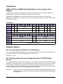
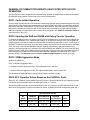
MPC823e Device Errata MPC823e Silicon Revision B.2—Mask Set 0J13D March 30, 2000 (Version 2) These errata apply to the MPC823e Revision B.2 (CDR2) silicon. The errata that are currently scheduled to be addressed in the future revision of the silicon are so marked. Changes to this errata are in italics. CPU ERRATA CPU1. Bus Error Not Fully Supported by the Data Cache on a Burst The data cache does not support a bus error that might occur on the second or third data beat of a burst. (burt_232). Workaround: Avoid using a bus error in this case. CPU2. Incorrect Data Breakpoint Detection on Store Instructions When a breakpoint on data occurs and you have programmed the size elements as byte or half-word, the following may occur: • A breakpoint might be detected when it should not • A breakpoint might not be detected when it should Either of these two cases can occur if the data that is programmed to be detected, matches some other portion of the register that is currently stored to memory by the store byte or store half-word instruction. For example: • Assume that you have programmed a byte data breakpoint on a store instruction and you are looking for the byte element 0x55. Assume that register R1 has the value 0x00080000, R10 has the value 0x55443322, and the stb R10,0x3(R1) store instruction is performed. What occurs is that byte 0x22 from R10 is stored to address 0x00080003, and this should not generate a breakpoint since 0x22 does not equal 0x55, but, in some cases, it can and does (in this scenario, R10 does include the data 0x55). The result is a breakpoint is executed when it should not be. This document contains information on a product under development. Motorola reserves the right to change or discontinue this product without notice. SEMICONDUCTOR PRODUCT INFORMATION 2000 Motorola, Inc.All Rights Reserved. • Assume that in the above case you are programming for byte element 0x22, maybe a breakpoint condition will not be detected, even though it should. (burt_246) Note: Workaround: These fault cases depend on the previous Load-Store instruction address. If the previous Load-Store instruction address’ LSB is different from the current instruction address’ LSB, then an incorrect breakpoint detection might occur. None. CPU3. Program Trace Mechanism Error In the following cases, there is an error in the program trace mechanism: • 0x00004ff0: divw. r25,r27,r26 • 0x00004ff4: divw. r28,r27,r26 • 0x00004ff8: unimplemented • 0x00004ffc: b 0x00005010 • and where: 0x00005010 belongs to a page where a page fault occurs The divide takes a relatively long time, so the instruction queue gets filled with the unimplemented instruction, which is the branch and the branch target (page fault). When the sequencer takes the unimplemented instruction, it releases the fetch that was blocked by the mmu error, which causes the queue to get another instruction in addition to the first page fault. Because the second fault is sequential to the branch target, it is not reported by the queue flush (VF) and this causes an incorrect value to be present in the VF flush information when the unimplemented exception occurs. (burt_251) Workaround: None. CPU4. Case of I-Cache Using Address of Old Page When Fetching New Page. The Instruction Cache uses the address associated with the old page when fetching the first data from a new page, under the following circumstances. 1.)There is a show cycle on a sequential instruction which crosses the page boundary. 2.)The internal bus is busy during the IMMU request with the old page number. Thus on the next cycle the I-Cache uses this incorrect address to access the external memory and internal cache. (burt_285) Workaround: 2 Do not run in “show all” mode or do not put a sequential instruction in the last address of an MMU page. MPC823e DEVICE ERRATA (REV. B.2) MOTOROLA CPM ERRATA CPM14. RCCR and RMDS Should Be Written To As A Single 32-bit Register The ERAM4K bit is cleared in the RISC Microcode Development Support Control Register, RMDS, if the register’s location is accessed as either part of a half-word or byte access. Workaround: If the ERAM4K is to be set, the RMDS must be accessed as part of a word starting at IMMR+0x9C4 to IMMR+0x9C7. It is best to write to these two registers as if they were a single 32-bit register. See register table below. RCCR-RMDS BIT FIELD 0 1 2 3 4 TIME RES 5 6 7 8 9 TIMEP DR2M DR1M 10 11 12 13 14 15 DRQP EIE SCD ERAM RESET 0 0 0 0 0 0 0 0 0 R/W R/W R/W R/W R/W R/W R/W R/W R/W R/W 28 29 ADDR BIT (IMMR & 0xFFFF0000) + 0x9c4 16 17 18 19 20 21 22 23 24 25 26 27 FIELD RESERVED ERAM4K RESERVED RESET 0 0 0 R/W R/W R/W R/W ADDR 30 31 (IMMR & 0xFFFF0000) + 0x9c6 GENERAL ERRATA G1. Core Operation Is Limited to a 3.0V Minimum The current versions of the MPC823e silicon are only tested and verified at 3.0V–3.6V power. Because of this, low voltage operation at 2.2V cannot be guaranteed to power the core. Workaround: None. G2. The External Bus Transaction May Hang After a PLPRCR Write Access An endless external bus transaction can occur on the next external bus access after executing a PLPRCR write command that changes the MF field. The PLPRCR write command causes the PLL to freeze the clocks until it is locked again, according to the new MF value. The failure mechanism occurs because the clock unit indicates operation complete before all necessary tasks are actually completed. The next external bus request is driven by the system interface unit and suddenly all clocks are stopped. Workaround: MOTOROLA The store instruction to the PLPRCR register should be in a burst-aligned address (cache line) followed by an isync instruction. The instruction cache should be enabled while executing this code sequence. MPC823e DEVICE ERRATA (REV.B.2) 3 G3. LCD Off and On Sequence With a Pending SDMA Cycle Causes Wrong Data Fetch If the LCD controller is turned off and there is a pending SDMA cycle for the LCD controller, and then the LCD is turned on again before the SDMA cycle completes, the LCD controller will start fetching from the start address + 16 instead of the start address. Workaround: Make sure that the pending SDMA cycle is completed before turning on the LCD controller. This can be done by performing an access to external memory before turning on the LCD controller. G6. LCD Controller Off Sequence When LAM Bit Is Set May Cause the CPU to Lock Up The LCD aggressive mode (LAM) bit of the SDCR register allows aggressive arbitration for the LCD controller when doing DMAs to system memory. If this bit is set and the LCD controller is turned off, the LCD controller generates a spurious request to the SDMA that may cause the CPU to lockup. Workaround: Clear the LAM bit before turning off the LCD controller. G7. Possible External Bus Hang Occurs Under Certain Error Conditions The external bus cycle may hang when the following sequence of events occur: 1. The transaction on the external bus ends as a result of TEA assertion OR a bus monitor timeout occurs. AND 2. The next transaction also ends with a TEA assertion or a bus monitor timeout. (burt 300) Workaround: None. G8. Higher Than Normal Current Consumption Without Executing a MULLW Instruction In the integer multiply module in the core, there are internal latches that do not get initialized properly during reset. Due to this improper initialization there is a 1:8 chance of a driver contention which may create higher than normal current consumption in various modes. This current consumption is most noticeable in the lower power modes. (burt_361) Workaround: Adding a mullw instruction puts the two control lines into a valid state, eliminating the contention. G12. Incorrect Reporting of Loss-of-Lock Reset Status. The RSR[LLRS] bit is set by both unintentional and software-initiated loss-of-lock. The RSR[LLRS] bit should be set only by an unintentional loss-of-lock. Software-initiated loss-of-lock (e.g. changing the SPLL multiplication factor or entering low-power modes) should not set this bit. Workaround: 4 The PLPRCR[SPLSS] functions as intended. Reference this bit instead. MPC823e DEVICE ERRATA (REV. B.2) MOTOROLA G13. Conflict Between Data Show Cycles and SDMA Burst Writes. IF data show cycles are enabled via SIUMCR[DSHW] ANDan internal register or dual-port RAM access is made immediately following an SDMA burst write, THEN the SDMA burst write may be corrupted. The observed phenomenon is that a burst write with four operands will hold the second operand into the third and fourth burst beats. For example, a burst write of A-B-C-D will be observed on the bus as A-B-B-B. Note: This behavior can also occur when the SDMA burst is to burst-inhibited memory. Setting the memory to burst-inhibited will not solve the problem. Workarounds: Do not use data show cycles in a system that performs SDMA bursts. These include systems that use ATM,Fast Ethernet, and memory-to-memory IDMA. G14. CPU Receives A Machine Check After Writing to the PLPRCR The CPU may receive a machine check after writing to the PLPRCR. This error is caused by an extra clock generated by the clock block after the SIU releases the bus. When the internal bus is released the CPU begins a transaction. The CPU’s clocks are then stopped mid-cycle and it never receives the acknowledge from the bus. The failure mechanism occurs due to an internal logic synchronization issue aggravated by memory refreshes performed by the UPM. The problem is only evident when entering and exiting doze mode frequently, such as when using doze to conserve power. The possibility of encountering this problem is small but finite (1 in a million entries). Workaround: Prevent the CPU from getting the bus during the extra clock. To do so you must enable the instruction cache and insert a delay. To calculate how long of a delay is necessary, take the longest bus transaction including memory refresh and PCMCIA (in CPU clocks). The resultant number of clocks must be executed using instructions such as NOP (1 clock), ISYNC (2 clocks) or DIVW (13 clocks). If you use the DIVW instruction, then divide the resultant number by 13 and round up. Then insert this many DIVW instructions (dividing by one) after the isync (see errata G9). If more than 2 DIVWs are required then the additional CACHE lines must be loaded and locked into the ICACHE. For example, If your longest transaction is 16 CPU clocks, then you must add 2 DIVW instructions: .global SetPLPRCR .align 16 SetPLPRCR: nop nop nop addi r5, r0, 1 stw r4, PLPRCR(r3) isync divw r4, r4, r5 divw r4, r4, r5 nop nop nop nop nop nop nop blr MOTOROLA #This cache line MUST be in the cache. #This cache line MUST be in the cache. #These NOP's are to prevent the CPU from #trying to fetch from the BLR target by #filling the instruction prefetch queue. #This cache line MUST be in the cache. MPC823e DEVICE ERRATA (REV.B.2) 5 G17. Address Bus May Consume Excess Current in Low Power Modes When entering Sleep or Deep Sleep Mode, normally PLPRCR[FIOPD] is set to 1 to enable internal pulldowns on the Address and Data Bus. In some units, the Address Bus pins are not sufficently pulled down. This may cause excess current draw. The Data Bus is not affected. Workaround: None. Fixed in Rev. B G18. Open Drain Pins Do Not Allow 5 Volt Pullups The Open Drain pins on the MPC823 will not allow external pullups to raise the voltage to the normal levels. Workaround: None. 6 MPC823e DEVICE ERRATA (REV. B.2) MOTOROLA GENERAL CUSTOMER INFORMATION Although not generally considered to be errata, the following items are guidelines for using the device appropriately. CI-100. External Interrupt Handling For external interrupt pins, if a request signal is a pulse, the interrupt request pin should be configured to “edge detect mode”. This ensures that the interrupt will be recognized even if interrupts are temporarily blocked or disabled by the software. The interrupt service routine (ISR) should clear the edge status flag after the ISR is entered and prior to setting the MSR’s EE bit (if it waits until after the EE bit is set, a second interrupt may be taken). If a request signal is a “standard handshake”, the assertion is asynchronous, but the negation occurs upon request from the ISR. This ensures that the interrupt is taken and the source of the interrupt is known. The timing with respect to the EE bit is the same. To avoid spurious interrupts, interrupt masks should not be set while interrupts might be sent to the core. Likewise, no interrupts should be disabled while the interrupt might be pending at the core. That way, when the core responds to the interrupt request, the request will still be pending and the core can determine the source of the interrupt. To accomplish all of the above, the EE bit should be disabled when masks are set or when interrupt enables are cleared. CI-101. Move to Special Register (mtspr) Access to ICTRL Register If you use mtspr to set the Ignore First Match (IFM) bit of the ICTRL register to 1 at the same time that you set an instruction breakpoint on this instruction, the chip will behave unpredictably. Workaround: Disable instruction breakpoints when setting the IFM bit. CI-102. Concurrent Operation Of Ethernet & I2C or SPI has Overlapping Parameter RAM Tables. When concurrent operation for the Ethernet protocol and either I2C or SPI is set up and used at the same timer, there is an overlap in the parameter RAM. Workaround: There is microcode available that moves the I2C/SPI parameter RAM entries to another location in the dual port RAM. To use this, download the description of the change and the object code file from the website at: http://www.mot.com/SPS/ADC/pps/_subpgs/_etoolbox/8XX/i2c_spi.html. This package is called the MPC8XX I2C/SPI Microcode Package. CI-103. Port A Pins (PA9 and PA11) May Consume Excess Current in Low Power Modes When the Port A pins PA9 and PA11 are configured as General Purpose Outputs, then the MPC823 may consume excess current in Sleep or Deep-Sleep mode due to internal floating nodes. Other than the 1mA of typical excess current, there are no operational issues. Workaround: Before entering Deep Sleep Mode, set PAPAR[DD9,DD11] and PADIR[DR9,DR11] to 1 to configure them as TDM pins. See Section 16.14.3 on page 16-470 of the MPC823 User's Manual. Be sure to read CI04 below. CI-104. PORT A PINS (PA9 AND PA11) MAY CONSUME EXCESS MOTOROLA MPC823e DEVICE ERRATA (REV.B.2) 7 CURRENT IN LOW POWER MODES WHILE IN TDM MODE When the Port A pins (PA9 and PA11) are configured as TDM pins, the MPC823 may consume excess current in Sleep or Deep Sleep modes. If the TDM is not active these pins are tristated, causing excess current consumption. Other than the 100 uA of typical excess current, there are no operational issues. Workaround: Set SIGMR[ENA] and SIMODE[STZA] to 1 before entering Sleep or Deep Sleep modes. See Section 16.7.5 on page 16-126 of the MPC823 User's Manual. 8 MPC823e DEVICE ERRATA (REV. B.2) MOTOROLA GENERAL DOCUMENTATION ERRATA ASSOCIATED WITH SILICON OPERATION The following items reflect additional information about the operation of the MPC823e and references made in the MPC823e User’s Manual. Please refer to the manual for clarification. DOC1. Cache-Inhibit Operation In some cases, the last instruction executed from a certain page gets the caching inhibited attribute of the next page when the page change occurs between the time a fetch request was issued to the instruction cache and the time the instruction cache delivers the instruction to the sequencer. Since the instruction cache-inhibit is only used for performance reasons (mostly for not caching very fast memories or pages that include non real-time programs), the performance effect of this feature is negligible. See Section 9 Instruction Cache for more information. (burt_237) DOC2. Updating the DAR and DSISR with Debug Counter Operation If a load/store breakpoint occurs as a result of debug counter expiration when oa machine check interrupt due to an error in a load/store cycle, a data storage interrupt, or an alignment interrupt occurs, set the DAR and DSISR registers to the effective address associated with the interrupting instruction. In some cases, when a load/store breakpoint occurs when one of the debug counters expires just before one of the above interrupts occur, the value of the DAR and DSISR is changed. Although the interrupt is after the breakpoint and, therefore, should be ignored by the processor, the DAR and DSISR are updated. The value of the DAR and DSISR is normally used by the software inside these interrupt routines and may influence program flow only if these interrupts are nested one inside the other and a load/store breakpoint is used inside one of these interrupt routines. See Section 6 Core and Section 20 Development Support for details. (burt_253) DOC3. SDMA Aggressive Mode Bit 25 of the SDCRLAM: LAM - LCD(Video) Aggressive Mode 0 = Disable LCD/Video aggressive mode. Priority depend on the LAID field. 1 = Enable LCD/Video aggressive mode. The LAID and RAID fields must be equal to 00. This bit affects all SDMA transfers including LCD and Video Controller transfers. D0C4. XFC Capacitor Values Based on the PLPRCRMF Field Table 5-4. XFC Capacitor Values Based on the MF Field in the PowerPC MPC823e User’s Manual on page 5-23 shows the recommended values for UDR2 (MPC823e rev. 0) silicon. The following table shows the recommended values for the XFC Capacitor for CDR2 (MPC823e rev. A and later) silicon, along with the minimum and maximum values, as determined by the multiplication factor (MF). XFC CAPACITOR VALUES MOTOROLA MF RANGE MINIMUM CAPACITANCE RECOMMENDED CAPACITANCE MAXIMUM CAPACITANCE UNIT MF =< 4 580 *MF - 100 680 * MF - 120 780 * MF - 140 pF MF > 4 830 * MF 1100 * MF 1470 * MF pF MPC823e DEVICE ERRATA (REV.B.2) 9 DOC5. I2C Address Register Not Cleared on Reset The I2C Address Regsiter (I2ADD) is not cleared by reset. This may cause a nonzero value to be present on reset. If this value matches the address of a slave device on the I2C bus, it will cause reception problems over I2C. This errata has no other effect on operation. Workaround: If using I2C Master Mode, reset I2ADD to 0x0 during your I2C initialization routine. 10 MPC823e DEVICE ERRATA (REV. B.2) MOTOROLA