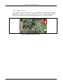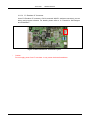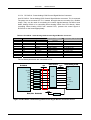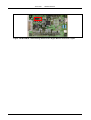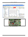
1
TSA-IC500
User's Manual
Date published: December 2012
Rev. 1.0
© TESSERA TECHNOLOGY INC. 2012
Printed in Japan
TS-TUM01606
TSA-IC500
USER'S MANUAL
CAUTION:
▪ The information in this document is subject to change without notice.
▪ No part of this document may be copied or reproduced in any form or by any means without prior written consent
of Tessera Technology Inc.
▪ Tessera Technology Inc. assumes no responsibility for inaccuracies or misprints of this document.
▪ Tessera Technology Inc. does not assume any liability for infringement of patents, copyrights, or other intellectual
property rights of third parties by or arising from the use of Tessera Technology Inc. products described in this
document. No license, express, implied or otherwise, is granted hereby under any patents, copyrights or other
intellectual property rights of Tessera Technology Inc. or others.
▪ Descriptions of circuits, software and other related information in this document are provided only to illustrate the
operation of semiconductor products and application examples. You are fully responsible for the incorporation of
these circuits, software, and information in the design of your equipment. Tessera Technology Inc. assumes no
responsibility for any losses incurred by you or third parties arising from the use of these circuits, software, or
information.
▪ This product should be handled like a CMOS semiconductor device. The user must take all precautions to avoid
build-up of static electricity while working with this equipment.
▪ All test and measurement tool including the workbench must be grounded.
▪ The user/operator must be grounded using the wrist strap.
▪ The device pins should not be touched with bare hands.
TESSERA TECHNOLOGY INC.
2/63
TSA-IC500
USER'S MANUAL
TABLE OF CONTENTS
1.
OVERVIEW.......................................................................................................................................6
1.1 Document Overview...................................................................................................................6
1.2 Terms in This Document............................................................................................................6
1.3 Board Features ..........................................................................................................................6
1.4 Product Overview.......................................................................................................................7
2.
HARDWARE...................................................................................................................................10
2.1 Hardware Specifications ..........................................................................................................10
2.2 Block Diagram..........................................................................................................................11
2.3 Power Supply...........................................................................................................................12
2.3.1
Power Options ...........................................................................................................12
2.3.2
Supply Power ............................................................................................................13
2.4 Smart Analog IC500.................................................................................................................14
2.5 Evaluation Circuit .....................................................................................................................16
2.5.1
Switch........................................................................................................................16
2.5.2
Clock Circuit ..............................................................................................................17
2.5.3
Consumption Current Measurement Terminal...........................................................18
2.5.4
Smart Analog IC500 Analog Peripheral Circuit..........................................................19
2.5.5
Connector ..................................................................................................................25
2.5.5.1 External Power Supply Connector..................................................................25
2.5.5.2 USB I/F Connector .........................................................................................26
2.5.5.3 E1 Emulator I/F Connector .............................................................................27
2.5.5.4 RL78/G1A - Smart Analog IC500 Control Signal Monitor Connector..............28
2.5.5.5 Extended Sensor I/F Connector .....................................................................30
2.5.5.6 Extended MCU I/F Connector.........................................................................33
3.
DEMONSTRATION OF PHOTOTRANSISTOR MOUNTED ON BOARD ......................................35
3.1 Tutorial for SA-Designer and CubeSuite+................................................................................35
3.1.1
Design Analog Frontend Circuit Using SA-Designer .................................................36
3.1.1.1 Start SA-Designer...........................................................................................36
3.1.1.2 Design Evaluation Circuit for Mounted Phototransistor ..................................37
3.1.2
Create Project Using CubeSuite+..............................................................................40
3.1.2.1 Download Sample Program (main.c)..............................................................40
3.1.2.2 Start CubeSuite+ ............................................................................................40
3.1.2.3 Create Project in CubeSuite+ .........................................................................40
3.1.3
Experience Using TSA-IC500....................................................................................46
3.1.3.1 Prepare Before Demonstration .......................................................................46
3.1.3.2 Demonstrate on Board ...................................................................................50
4.
HARDWARE MATERIALS .............................................................................................................55
4.1 Circuit Diagrams ......................................................................................................................55
TESSERA TECHNOLOGY INC.
3/63
TSA-IC500
USER'S MANUAL
4.2 Parts List..................................................................................................................................59
4.3 Board Size ...............................................................................................................................61
4.4 Parts Layout.............................................................................................................................62
TESSERA TECHNOLOGY INC.
4/63
TSA-IC500
USER'S MANUAL
FIGURES AND TABLES
Figure 1.1 Board (Front Side)...................................................................................................................7
Figure 1.2 Board (Back Side) ...................................................................................................................8
Figure 1.3 Product Usage Sample Image 1..............................................................................................9
Figure 1.4 Product Usage Sample Image 2..............................................................................................9
Figure 2.1 TSA-IC500 Block Diagram ....................................................................................................11
Figure 2.2 JP1 Setting ............................................................................................................................12
Figure 2.3 LED Indicator (USB Power Supply).......................................................................................13
Figure 2.4 LED Indicator (External Power Supply) .................................................................................13
Figure 2.5 Switch Layout ........................................................................................................................16
Figure 2.6 Clock Circuit Layout ..............................................................................................................17
Figure 2.7 RL78/G1A Current Measurement Terminal ...........................................................................18
Figure 2.8 Smart Analog IC500 Current Measurement Terminal ...........................................................18
Figure 2.9 Amplifier Peripheral Circuit 1: AMP1 .....................................................................................19
Figure 2.10 Amplifier Peripheral Circuit 2: AMP2 ...................................................................................20
Figure 2.11 Amplifier Peripheral Circuit 3: AMP3 ...................................................................................21
Figure 2.12 Amplifier Peripheral Circuit 4 ...............................................................................................22
Figure 2.13 Example of Mounting Resistance for Voltage-dividing Circuit to Amplifier Peripheral Circuit
4 .............................................................................................................................................................23
Figure 2.14 Amplifier Peripheral Circuit 5 ...............................................................................................24
Figure 2.15 Amplifier Peripheral Circuit 6 ...............................................................................................24
Figure 2.16 External Power Supply Connector Layout ...........................................................................25
Figure 2.17 USB I/F Connector Layout ..................................................................................................26
Figure 2.18 E1 Emulator I/F Connector Layout ......................................................................................27
Figure 2.19 RL78/G1A - Smart Analog IC500 Control Signal Monitor Connector Circuit .......................28
Figure 2.20 RL78/G1A - Smart Analog IC500 Control Signal Monitor Connector Layout.......................29
Figure 2.21 Extended Sensor I/F Connector Layout ..............................................................................31
Figure 2.21 TSA-IC500 connecting the sensor extension board TSA-EXT BOARD ..............................31
Figure 2.22 Extended MCU I/F Connector Layout..................................................................................34
Figure 3.1 Phototransistor Position ........................................................................................................54
Figure 4.1 Board Size.............................................................................................................................61
Figure 4.2 Parts Layout (front side) ........................................................................................................62
Figure 4.3 Parts Layout (back side)........................................................................................................63
Table 1.1 List of Terms.............................................................................................................................6
Table 2.1 Hardware Specifications.........................................................................................................10
Table 2.2 Power Supply Settings ...........................................................................................................12
Table 2.3 Smart Analog IC500 Terminal List..........................................................................................14
Table 2.4 Switch Functions ....................................................................................................................16
Table 2.5 Connector Function List..........................................................................................................25
Table 2.6 RL78/G1A - Smart Analog IC500 Control Signal Monitor Connector......................................28
Table 2.7 Extended Sensor I/F Connector .............................................................................................30
Table 2.8 Extended MCU I/F Connector.................................................................................................33
TESSERA TECHNOLOGY INC.
5/63
TSA-IC500
USER'S MANUAL
1. Overview
1.1
Document Overview
This document describes the hardware specifications, software structure, and USB driver
installation for TSA-IC500. It describes an example of analog front end circuit design using
mounted phototransistor at the end.
1.2
Terms in This Document
This document uses following teams for explaining the hardware specifications and software.
Table 1.1 List of Terms
Term
Smart Analog
Smart Analog IC
Smart Analog IC500
GUI “Smart Analog Easy Starter”
E1 emulator
CubeSuite+
SA-Designer
1.3
Description
Product that analog circuits and features are
reconfigurable by software designed for supporting
multiple sensors and drivers.
Product that is categorized in above term, but it is a
package of an analog circuit.
Smart Analog IC (reconfigurable circuit type) from
Renesas Electronics.
Smart Analog IC500 official part number: RAA730500
Development tool for RL78/G1E Stick
On-chip debugging emulator from Renesas Electronics.
This can be used as a flash programmer. (selling
separately)
Integrated development environment packaging all basic
software tools for developing software on
microcontrollers form Renesas Electronics.
Development tool from Renesas Electronics. It generates
circuit data as C source code from the analog frontend
circuit designs of Smart Analog product.
Board Features
•
•
•
•
•
Enable to evaluate Smart Analog IC500 (RAA730500) from Renesas Electronics.
CPU RL78/G1A (R5F10ELEAFB) is mounted for controlling Smart Analog IC500.
Option to use USB power or external power supply.
Enable to get illuminance of phototransistor with using “Smart Analog Easy Starter”.
Extensibility to add sensors.
TESSERA TECHNOLOGY INC.
6/63
TSA-IC500
1.4
USER'S MANUAL
Product Overview
The product contains following items.
•
TSA-IC500
•
Documentations
This contains some specific notes and downloading URLs for “Smart Analog Easy
Starter” and USB driver. Please read this before start using.
•
USB cable (Mini-B type)
The pictures of the board are shown below.
Figure 1.1 Board (Front Side)
TESSERA TECHNOLOGY INC.
7/63
TSA-IC500
USER'S MANUAL
Figure 1.2 Board (Back Side)
TESSERA TECHNOLOGY INC.
8/63
TSA-IC500
USER'S MANUAL
The product usage sample is shown below. It can design the analog part of RAA730500 by using
“Smart Analog Easy Starter”. Also, you can design with using “CubeSuite+” and “SA-Designer”
when you connect E1 emulator. For details about "CubeSuite+" and "SA-Designer" such as
operations of them, please refer to Renesas Electronics Web site .
GUI Smart Analog Easy Starter
Circuit Design
Waveform
Observation
USB Cable
Figure 1.3 Product Usage Sample Image 1
IDE CubeSuite+
SA-Designer
PC
USB Cable
TSA-IC500
E1 Emulator
( On-chip debugging emulator )
Figure 1.4 Product Usage Sample Image 2
TESSERA TECHNOLOGY INC.
9/63
TSA-IC500
USER'S MANUAL
2. Hardware
2.1
Hardware Specifications
The specifications of the product are described in below table.
Table 2.1 Hardware Specifications
Smart Analog IC
CPU
Operation Frequency
Interface
Sensor Input Terminal
Supply Voltage
Indication
Mounted Sensor
Product Size
TESSERA TECHNOLOGY INC.
Specification
Smart Analog IC500 (RAA730500) from Renesas
Electronics
Smart Analog IC, reconfigurable circuit
RL78/G1A (R5F10ELEAFB) from Renesas Electronics
(Flash ROM: 64KB, RAM: 4KB, Data Flash: 4KB)
Main system clock:
High-speed on-chip oscillator 1-32MHz
Low-speed on-chip oscillator 15kHz
Sub system clock:
Oscillator 32.768kHz
USB connector (Mini-B)
External power connector
E1 emulator connector
RL78/G1A-Smart Analog IC500 control signal monitor
connector
Extended sensor I/F connector (50-pin)
Extended MCU I/F connector (50-pin)
12 terminals:
MPXIN10/11/20/21/30/31/40/41/50/51/60/61
It can input up to (A_GND – 0.1V)- (AVCC-1.5V)
+5.0V (USB or external power supply)
LED
Phototransistor (SFH3710-3/4-Z from OSRAM)
Board size:
90 x 55 mm (W x D)
10/63
TSA-IC500
2.2
USER'S MANUAL
Block Diagram
The block diagram of TSA-IC500 is shown below.
SW2
Reset
Switch
Digital Power Area
Digital Power Area
CN3
Analog Power Area
E1 Emulator I/F
Connector
Reset
Circuit
TH1
RL78/G1A-Smart Analog IC500
Control Signal Monitor Connector
IC3
VBUS
UVCC
IC4
VCC
Regulator
XI/XO
RL78/G1A
TOOL0
RESET
XTAL1
12MHz
USB
Controller
ADP151-AUJZ-3.3 U_GND
(Non Mount)
IC1
MAX3420EETG+
IC2
AVDD
Smart Analog
IC500
LDO_OUT
VDD
AVCC
AVDD
VDD
DVCC
CN2
DVDD
USB
I/F
CN
D+/D-
UX60SC-MB-5ST
IC6
SCLK/MISO
SCLK/MISO
MOSI/SS
MOSI/SS
Control
Control
Port
VDD
Voltage
Level
Shifter
DVCC
I/F
IC7
UVCC
/RESET
RESET IC
Analog
Port
Port
P04
ADM1816-10ARTZ
MPXIN20
Q1
Power Branch
VBUS
JP1 Area
SFH3710-3/4-Z
TH3
External Power
Area
+5V
DGND
AVCC
Power
Option
Power
Connector
Sensor
Phototransistor
X1/X2 XT1/XT2 Port
DVCC
DVCC
GND
UVCC
VDD
Extended MCU I/F
Connector
IC9
Analog Power
直結抵抗
U_GND
DGND
Extended Sensor
I/F Connector
XTAL3
Regulator
ADP151-AUJZ-3.3
AGND
VDD
TH2
32.768KHz
XTAL2
Analog Power Area
No Mount
Area
Figure 2.1 TSA-IC500 Block Diagram
This board mounts RL78/G1A for the control microcontroller of Smart Analog IC500. To
minimize noises, it uses separate power plane.
•
External Power Area:
Area that supplies DC power from external power.
•
Power Branch Area:
Area that supplies power to digital power area and analog power area with selecting from
USB power or external power.
•
Digital Power Area:
Area that supplies power to USB controller, RL78/G1A and logic circuit.
•
Analog Power Area:
Area that supplies power to analog power of Smart Analog IC500 and RL78/G1A.
TESSERA TECHNOLOGY INC.
11/63
TSA-IC500
2.3
USER'S MANUAL
Power Supply
2.3.1
Power Options
This board has a function to be able to select a power source. Following table and figure
describe how to set a power source. It is set to USB power supply as default.
Table 2.2 Power Supply Settings
Power Source
External
power supply
(+5.0V) *
USB
power
supply
(+5.0V)
JP1 Setting
5-3 short
6-4 short
1-3 short
2-4 short
Connector
Reference
CN1
Connector Form
2.5mm-pitch dipole connector
Connector Part
Number
B2P-SHF-1AA
CN2
USB Mini-B connector
UX60SC-MB-5ST
1
2
3
4
5
6
1
2
3
4
5
6
USB Power Supply
External Power Supply
Figure 2.2 JP1 Setting
*Do not apply voltage other than +5.0V. The board is not guaranteed to work.
TESSERA TECHNOLOGY INC.
12/63
TSA-IC500
2.3.2
USER'S MANUAL
Supply Power
LED will turn on when you supply power to the board. If it is USB power supply, both LED1
and LED2 will turn on. If it is external power supply, only LED2 will turn on.
LED1 turn on
LED2 turn on
Figure 2.3 LED Indicator (USB Power Supply)
LED1 turn off
LED2 turn on
Figure 2.4 LED Indicator (External Power Supply)
TESSERA TECHNOLOGY INC.
13/63
TSA-IC500
2.4
USER'S MANUAL
Smart Analog IC500
The connecting destinations of all Smart Analog IC500 terminals are described below.
Table 2.3 Smart Analog IC500 Terminal List
Smart
Analog
IC500
Pin No.
1
2
3
AVDD3
SC_IN
CLK_SYNCH
AVCC
UMBL_SCIN
SAIC_CLKSYNCH
4
SYNCH_OUT
UMBL_SYNCOUT
Analog power
Extended sensor I/F connector
RL78/G1A P41 (4pin) through
Level Shifter
Extended sensor I/F connector
5
6
AGND2
GAINAMP_OUT
A_GND
UMBL_GAMPOUT
Analog power
Extended sensor I/F connector
7
8
9
10
11
12
GAINAMP_IN
MPXIN61
MPXIN51
MPXIN60
MPXIN50
AMP3_OUT
UMBL_GAMPIN
UMBL_MPXIN61
UMBL_MPXIN51
UMBL_MPXIN60
UMBL_MPXIN50
UMBL_AMP3OUT
Extended sensor I/F connector
Extended sensor I/F connector
Extended sensor I/F connector
Extended sensor I/F connector
Extended sensor I/F connector
Extended sensor I/F connector
13
UMBL_DAC3OUT
Extended sensor I/F connector
14
DAC3_OUT /
VREFIN3
AMP2_OUT
UMBL_AMP2OUT
Extended sensor I/F connector
15
16
AGND1
AMP1_OUT
A_GND
UMBL_AMP1OUT
Analog power
Extended sensor I/F connector
17
18
AVCC
UMBL_DAC2OUT
Analog power
Extended sensor I/F connector
UMBL_DAC1OUT
Extended sensor I/F connector
-
20
21
22
23
24
25
26
27
28
29
30
31
AVDD1
DAC2_OUT /
VREFIN2
DAC1_OUT /
VREFIN1
MPXIN41
MPXIN31
MPXIN40
MPXIN30
MPXIN21
MPXIN11
MPXIN20
MPXIN10
AGND3
BGR_OUT
AVDD2
LDO_OUT
RL78/G1A ANI6
(50pin)
RL78/G1A ANI7
(49pin)
-
UMBL_MPXIN41
UMBL_MPXIN31
UMBL_MPXIN40
UMBL_MPXIN30
UMBL_MPXIN21
UMBL_MPXIN11
UMBL_MPXIN20
UMBL_MPXIN10
A_GND
BGR_OUT
AVCC
UMBL_VREFOUT
Extended sensor I/F connector
Extended sensor I/F connector
Extended sensor I/F connector
Extended sensor I/F connector
Extended sensor I/F connector
Extended sensor I/F connector
Extended sensor I/F connector
Extended sensor I/F connector
Analog power
Grounded through C42 (0.1uF)
Analog power
Extended sensor I/F connector
32
AMP4_OUT
UMBL_AMP4OUT
Extended sensor I/F connector
33
34
35
AMP4_INN
AMP4_INP
TEMP_OUT
UMBL_AMP4_IN_NE
UMBL_AMP4_IN_PO
UMBL_TMPOUT
Extended sensor I/F connector
Extended sensor I/F connector
Extended sensor I/F connector
36
RESET
SAIC_/RESET
RL78/G1A-Smart Analog
IC500 control signal monitor
connector through Level
Shifter
RL78/G1A AVDD
(47pin) through EF5
RL78/G1A ANI5
(51pin)
RL78/G1A ANI17
(60pin)
RL78/G1A P130
(57pin)
19
Smart Analog
IC500
Terminal Name
TESSERA TECHNOLOGY INC.
Circuit Signal Name
Destination 1
Destination 2
RL78/G1A ANI19
(1pin)
RL78/G1A ANI16
(59pin)
Amp peripheral circuit
Amp peripheral circuit
Amp peripheral circuit
Amp peripheral circuit
RL78/G1A ANI2
(54pin)
-
14/63
TSA-IC500
37
38
DVDD
SCLK
DVCC
SAIC_SCLK
39
SDO
UMBL_SDO
40
SDI
SAIC_SDI
41
CS
SAIC_/CS
42
43
44
DGND
DAC4_OUT /
VREFIN4
HPF_OUT
45
USER'S MANUAL
RL78/G1A SCK21
(29pin)
D_GND
UMBL_DAC4OUT
Digital power
RL78/G1A-Smart Analog
IC500 control signal monitor
connector through Level
Shifter
RL78/G1A-Smart Analog
IC500 control signal monitor
connector
RL78/G1A-Smart Analog
IC500 control signal monitor
connector through Level
Shifter
RL78/G1A-Smart Analog
IC500 control signal monitor
connector through Level
Shifter
Digital power
Extended sensor I/F connector
UMBL_HPFOUT
Extended sensor I/F connector
CLK_HPF
SAIC_CLKHPF
46
CLK_LPF
SAIC_CLKLPF
47
48
AGND4
LPF_OUT
A_GND
UMBL_LPFOUT
RL78/G1A TO00 (61pin)
through Level Shifter
RL78/G1A TO04 (3pin)
through Level Shifter
Analog power
Extended sensor I/F connector
RL78/G1A ANI4
(52pin)
-
TESSERA TECHNOLOGY INC.
RL78/G1A SI21 (28pin)
RL78/G1A SO21
(27pin)
RL78/G1A P73 (26pin)
-
RL78/G1A ANI3
(53pin)
15/63
TSA-IC500
2.5
USER'S MANUAL
Evaluation Circuit
This section describes the evaluation circuit on the board.
2.5.1
Switch
The board has 2 kinds of switches shown below table.
Table 2.4 Switch Functions
Reference
Function
SW1
Switch for external interrupts
Connecting to INTP0 terminal of RL78/G1A
Inputting High level to INTP0 terminal when releasing the switch, and
Low level when pushing down the switch.
Switch for board reset
Connecting to RESET terminal of RL78/G1A
Inputting High level to RESET terminal when releasing the switch, and
Low level when pushing down the switch.
MCU becomes reset status when Low level.
SW2
SW2
SW1
(Switch for board reset )
(Switch for external interrupts )
Figure 2.5 Switch Layout
TESSERA TECHNOLOGY INC.
16/63
TSA-IC500
2.5.2
USER'S MANUAL
Clock Circuit
RL78/G1A, mounted on this board, has a high-speed oscillator built-in as system clock. This board
does not have a normal oscillator since use of high-speed built-in oscillator circuit is assumed. The
pattern (XTAL2) is built on the board in case that frequency accuracy and frequency itself cannot meet
the requirements. Lead type two/three terminal oscillator can be implemented. Also, XTAL3
(32.768kHz) is mounted as a sub clock.
Oscillator for
Subsystem clock
Through-hole ground
(Three-terminal oscillator )
Through-hole for
mounting oscillator
Footprint for mounting
capacitor
Figure 2.6 Clock Circuit Layout
TESSERA TECHNOLOGY INC.
17/63
TSA-IC500
2.5.3
USER'S MANUAL
Consumption Current Measurement Terminal
There are measurement terminals on the board to measure consumption current for
RL78/G1A and Smart Analog IC500. Disconnect 0Ω resistance (R20/R60/R89) before
measuring the consumption current.
VDD
TP9
TP10
RL78/G1A
VDD
VDD
R20
0Ω
EVDD0
Figure 2.7 RL78/G1A Current Measurement Terminal
AVDD1,2,3
DVDD
TP11
AVCC
TP12
IC500
R60
0Ω
TP13
DVCC
Smart Analog
AVDD1
AVDD2
AVDD3
TP14
DVDD
R89
0Ω
Figure 2.8 Smart Analog IC500 Current Measurement Terminal
TESSERA TECHNOLOGY INC.
18/63
TSA-IC500
2.5.4
USER'S MANUAL
Smart Analog IC500 Analog Peripheral Circuit
Smart Analog IC500 on the board has an operational amplifier, which has a resistance
built-in for variable gain. Also, patterns are designed on the board for the case of connecting
other parts. The size of a resistance should be 1608. Those resistances without constant
mean that they are not mounted.
AVCC
R72
R71
R59
R58
R57
R56
MPXIN10
UMBL_MPXIN10
MPXIN11
UMBL_MPXIN11
-
AMP1_OUT
UMBL_AMP1OUT
+
MPXIN20
R61
MPXIN20
MPXIN21
UMBL_MPXIN21
R70
R69
R68
R67
R62
A_GND
UMBL_AMP2OUT
R63
AVCC
Q1
0ohm
R64
R73
R65
UMBL_AMP3OUT
R66
470ohm
A_GND
Figure 2.9 Amplifier Peripheral Circuit 1: AMP1
*
Caution:
A phototransistor is connected to the input terminal MPXIN20 in the built-in operational
amplifier AMP1. To connect other sensor, please disconnect R62. Mount the disconnected
resistance to R61.
TESSERA TECHNOLOGY INC.
19/63
TSA-IC500
USER'S MANUAL
AVCC
R85
R84
R77
R76
R75
R74
MPXIN30
UMBL_MPXIN30
MPXIN31
UMBL_MPXIN31
-
AMP2_OUT
UMBL_AMP2OUT
+
MPXIN40
UMBL_MPXIN40
MPXIN41
UMBL_MPXIN41
R83
R82
UMBL_AMP1OUT
R81
R80
A_GND
R79
R78
R86
UMBL_AMP3OUT
R87
Figure 2.10 Amplifier Peripheral Circuit 2: AMP2
TESSERA TECHNOLOGY INC.
20/63
TSA-IC500
USER'S MANUAL
AVCC
R114
R113
R99
R98
R97
R96
MPXIN50
UMBL_MPXIN50
MPXIN51
UMBL_MPXIN51
-
AMP3_OUT
UMBL_AMP3OUT
+
MPXIN60
UMBL_MPXIN60
MPXIN61
UMBL_MPXIN61
R112
R111
UMBL_AMP1OUT
R110
R109
A_GND
R101
R100
R103
UMBL_AMP2OUT
R102
Figure 2.11 Amplifier Peripheral Circuit 3: AMP3
TESSERA TECHNOLOGY INC.
21/63
TSA-IC500
USER'S MANUAL
Analog signal of Smart Analog IC500 is connected to the input terminal of A/D converter in
RL78/G1A. The pattern is mounted to be able to connect parts between Smart Analog IC500
and RL78/G1A. The size of parts should be 1608. A voltage-dividing resistance circuit and
clamp circuit can be mounted.
The patterns in below figure are mounted on Smart Analog IC500 terminals in below table.
Those resistances without constant mean that they are not mounted.
Smart Analog IC500
Terminal
AMP1_OUT
AMP2_OUT
AMP3_OUT
AMP4_OUT
HPF_OUT
LPF_OUT
GAINAMP_OUT
SYNCH_OUT
RL78/G1A
Reference
Cx
C28
C29
C56
C57
C58
C59
C55
C61
Reference
Dx
D2
D3
D4
D5
D6
D7
D1
D8
Reference
Ry
R120
R121
R122
R123
R124
R125
R119
R117
Reference
Rz
R129
R130
R131
R132
R133
R134
R128
R126
Smart Analog IC500
RL78_AVDD
RL78_AVDD
AVDD
ADC Input
Reference
Rx
R24
R25
R29
R26
R27
R28
R23
R21
Dx
Ry
0ohm
Rx
0ohm
Cx
Analog Output
Rz
A_GND
Figure 2.12 Amplifier Peripheral Circuit 4
TESSERA TECHNOLOGY INC.
22/63
TSA-IC500
USER'S MANUAL
With the ADC limitation of RL78/G1A, the maximum voltage that can apply to ADC is 3.3V.
The analog terminal of Smart Analog IC500 can output maximum of 5V. Because of this, the
pattern is mounted to be able to connect parts between Smart Analog IC500 and RL78/G1A,
and a voltage-dividing circuit can be mounted. As an example, the formula, for evaluating the
analog voltage from the analog terminal of Smart Analog IC500 when a voltage-dividing
resistance is mounted, is described below.
The formula to evaluate analog voltage from A/D conversion value (A/D conversion value
register (ADCR 12bit)) is shown below.
Analog Voltage1 =
A/D conversion value
12
2 -1
× RL78_AVDD
Analog Voltage1: A/D converter input voltage (V)
RL78_AVDD: A/D converter power voltage (V)
Analog Voltage1 divides output voltage from the analog terminal of Smart Analog IC500 by
resistance. Thus, following formula describes the output voltage of analog terminal.
( Ry + Rz)
Analog Voltage2 = Analog Voltage1×
Rz
Analog Voltage2: Output voltage (V) from analog terminal of Smart Analog IC500
In practice, the effect of resistance errors should be taken into consideration in above
formula.
RL78/G1A
AVDD
ADC Input
Smart Analog IC500
RL78_AVDD
RL78_AVDD
Dx
Ry
2kohm
Rx
0ohm
Cx
Analog Output
Rz
3kohm
A_GND
Figure 2.13 Example of Mounting Resistance for Voltage-dividing Circuit to Amplifier Peripheral
Circuit 4
TESSERA TECHNOLOGY INC.
23/63
TSA-IC500
USER'S MANUAL
Smart Analog IC500 terminal mounts patterns shown below figure.
•
TEMP_OUT
Smart Analog IC500
RL78/G1A
P02/ANI17
R22
0ohm
TEMP_OUT
Figure 2.14 Amplifier Peripheral Circuit 5
Smart Analog IC500 terminal mounts patterns shown below figure. RL78/G1A and Smart
Analog IC500 are connected through a level-shifter with two power supply type to accept the
voltage error between them.
•
CLK_HPF
•
CLK_LPF
•
CLK_SYNCH
RL78/G1A
VDD
SN74LVC2T45
DVCC
DVDD
VDD
Timer Output
Smart Analog IC500
Voltage
Level
Shifter
Clock Input
Figure 2.15 Amplifier Peripheral Circuit 6
TESSERA TECHNOLOGY INC.
24/63
TSA-IC500
2.5.5
USER'S MANUAL
Connector
The board mounts many kinds of connectors. (Some parts are not mounted.) The table
below describes the connectors.
Table 2.5 Connector Function List
Connector
Reference
CN1
Connector Form
2.5mm-pitch dipole connector
Connector Part
Name
B2P-SHF-1AA
CN2
CN3
TH1
USB Mini-B connector
2.54mm-pitch 14-pole connector
2.54mm-pitch 10-pole connector
UX60SC-MB-5ST
7614-6002PL
Not mounted
TH2
TH3
2.54mm-pitch 50-pole connector
2.54mm-pitch 50-pole connector
Not mounted
Not mounted
Function
External power supply
(+5.0V apply)
USB I/F
E1 emulator I/F
RL78/G1A - Smart Analog
IC500 control signal
monitor
Extended sensor I/F
Extended MCU I/F
2.5.5.1 External Power Supply Connector
As an external power supply connector, CN1 is mounted. Apply +5.0V with caring about
plus and minus. For detail about selecting power sources from external power or USB
power, please refer to “2.3.1 Power Options”.
Figure 2.16 External Power Supply Connector Layout
TESSERA TECHNOLOGY INC.
25/63
TSA-IC500
USER'S MANUAL
2.5.5.2 USB I/F Connector
As an USB I/F connector, CN2 is mounted. It is connected to PC through USB controller
(MAX3420). The cable is bundled, so please use it. For detail about selecting power
sources from external power or USB power, please refer to “2.3.1 Power Options”.
Figure 2.17 USB I/F Connector Layout
TESSERA TECHNOLOGY INC.
26/63
TSA-IC500
USER'S MANUAL
2.5.5.3 E1 Emulator I/F Connector
As an E1 Emulator I/F connector, CN3 is mounted. With E1 emulator connected, you can
debug and program software. For details, please refer to “3.1Tutorial for SA-Designer
and CubeSuite+”.
Figure 2.18 E1 Emulator I/F Connector Layout
*
Caution:
Do not supply power from E1 emulator. It may cause the board breakdown.
TESSERA TECHNOLOGY INC.
27/63
TSA-IC500
USER'S MANUAL
2.5.5.4 RL78/G1A - Smart Analog IC500 Control Signal Monitor Connector
As a RL78/G1A - Smart Analog IC500 Control Signal Monitor connector, TH1 is mounted.
The parts are not mounted for TH1. Instead, through-holes are mounted for a flexible
usage. They can be used for monitoring the control signals between RL78/G1A and
Smart Analog IC500 or for controlling Smart Analog IC500 from CPU directly. When
controlling Smart Analog IC500 from external CPU, process the control signal of
RL78/G1A on the board appropriately.
Table 2.6 RL78/G1A - Smart Analog IC500 Control Signal Monitor Connector
TH1
Pin No.
1
2
3
4
5
6
7
8
9
10
Smart Analog IC500
Terminal No.
Signal Name
38
SCLK
39
SDO
40
SDI
41
CS
36
RESET
3
CLK_SYNCH
46
CLK_LPF
45
CLK_HPF
-
Signal Name on Circuit
Diagram
UMBL_SCLK
UMBL_SDO
UMBL_SDI
UMBL_CS
UMBL_RESET
UMBL_CLKSYNC
UMBL_CLKLPF
UMBL_CLKHPF
D_GND
D_GND
Connection with RL78/G1A
To 29-Pin SCK21
To 28-Pin SI21
To 27-Pin SO21
To 26-Pin P73
To 57-Pin P130
To 4-Pin TO07
To 3-Pin TO04
To 61-Pin TO00
-
The red frame parts below are connected to TH1.
RL78/G1A
VDD
SN74LVC2T45
DVCC
Smart Analog IC500
DVDD
VDD
SCLK21
R37
SCLK
SO21
R39
SDI
P73
R40
CS
L/S
TO00
R34
TO04
R35
CLK_LPF
TO07
R36
CLK_SYNCH
P130
R32
RESET
SI21
R38
SDO
CLK_HPF
VDD
R32、R34−R40 0ohm
R92
10kohm
Figure 2.19 RL78/G1A - Smart Analog IC500 Control Signal Monitor Connector Circuit
TESSERA TECHNOLOGY INC.
28/63
TSA-IC500
USER'S MANUAL
Figure 2.20 RL78/G1A - Smart Analog IC500 Control Signal Monitor Connector Layout
TESSERA TECHNOLOGY INC.
29/63
TSA-IC500
USER'S MANUAL
2.5.5.5 Extended Sensor I/F Connector
As an extended sensor I/F connector, TH2 is mounted. The parts are not mounted for
TH2. Instead, through-holes are mounted for a flexible usage.
Table 2.7 Extended Sensor I/F Connector
TH2
Pin
No.
1
3
5
7
9
11
13
15
17
19
21
23
25
27
29
31
33
35
37
39
41
43
45
47
49
Smart Analog IC500
Terminal Signal Name
No.
19
DAC1OUT
16
AMP1OUT
27
MPXIN10
25
MPXIN11
26
MPXIN20
24
MPXIN21
18
DAC2OUT
14
AMP2OUT
23
MPXIN30
21
MPXIN31
22
MPXIN40
20
MPXIN41
13
DAC3OUT
12
AMP3OUT
11
MPXIN50
9
MPXIN51
10
MPXIN60
8
MPXIN61
33
AMP4_INN
34
AMP4_INP
43
DAC4OUT
32
AMP4_OUT
TESSERA TECHNOLOGY INC.
Signal Name on Circuit
Diagram
TH2
Pin
No.
UMBL_DAC1OUT
2
UMBL_AMP1OUT
4
A_GND
6
UMBL_MPXIN10
8
UMBL_MPXIN11
10
UMBL_MPXIN20
12
UMBL_MPXIN21
14
UMBL_DAC2OUT
16
UMBL_AMP2OUT
18
A_GND
20
UMBL_MPXIN30
22
UMBL_MPXIN31
24
UMBL_MPXIN40
26
UMBL_MPXIN41
28
UMBL_DAC3OUT
30
UMBL_AMP3OUT
32
A_GND
34
UMBL_MPXIN50
36
UMBL_MPXIN51
38
UMBL_MPXIN60
40
UMBL_MPXIN61
42
UMBL_AMP4OUT_IN_NE 44
UMBL_AMP4OUT_IN_PO 46
UMBL_DAC4OUT
48
UMBL_AMP4OUT
50
Smart Analog IC500
Terminal Signal Name
No.
35
TEMP_OUT
44
HPF_OUT
48
LPF_OUT
4
SYNCH_OUT
6
GAINAMP_OUT
2
SC_IN
7
GAINAMP_IN
31
LDO_OUT
-
Signal Name on
Circuit Diagram
AVCC
A_GND
A_GND
No connection
No connection
No connection
RL78_AVDD
RL78_AVREFP
RL78_AVREFM
RL78_ANI8
RL78_ANI9
RL78_ANI10
RL78_ANI11
RL78_ANI12
UMBL_TMPOUT
UMBL_HPFOUT
UMBL_LPFOUT
UMBL_SYNCOUT
UMBL_GAMPOUT
UMBL_SCIN
UMBL_GAMPIN
UMBL_VREFOUT
A_GND
A_GND
AVCC
30/63
TSA-IC500
USER'S MANUAL
Figure 2.21 Extended Sensor I/F Connector Layout
We are selling the sensor extension board. This board is connected to Extended Sensor
I/F Connector(TH2). Pin header is included with the board. Please mount the TH2 this
pin header. Should be implemented in the same plane as the CN3(E1 Emulator I/F
Connector). You can be extension by a sensor used in combination with TSA-IC500 as
in TSA-EXT BOARD.
Figure 2.22 TSA-IC500 connecting the sensor extension board TSA-EXT BOARD
*
TSA-EXT BOARD is not attached to the TSA-IC500. Please purchase separately.
TESSERA TECHNOLOGY INC.
31/63
TSA-IC500
USER'S MANUAL
It is a list of connecting signal TSA-EXT BOARD and TSA-IC500.
TSA-IC500
TH2
TH2
Pin
TSA-EXT BOARD
Pin
Signal
19
DAC1OUT
CN1-1
TH1-1
2
Analog Power
CN1-2
TH1-2
3
16
AMP1OUT
CN1-3
TH1-3
4
Analog GND
CN1-4
TH1-4
Analog GND
Pin
Smart Analog IC500
1
Signal
CN1-5
TH1-5
6
Analog GND
CN1-6
TH1-6
7
27
MPXIN10
CN1-7
TH1-7
8
N.C
CN1-8
TH1-8
9
25
MPXIN11
CN1-9
TH1-9
10
N.C
CN1-10
TH1-10
11
26
MPXIN20 *
CN1-11
TH1-11
12
N.C
CN1-12
TH1-12
13
24
MPXIN21
CN1-13
TH1-13
14
- (RL78_AVDD) **
CN1-14
TH1-14
15
18
DAC2OUT
CN1-15
TH1-15
16
- (RL78_AVREFP) **
CN1-16
TH1-16
17
14
AMP2OUT
CN1-17
TH1-17
18
- (RL78_AVREFM) **
CN1-18
TH1-18
CN1-19
TH1-19
20
- (RL78_ANI8) **
CN1-20
TH1-20
19
Analog GND
21
23
MPXIN30
CN1-21
TH1-21
22
- (RL78_ANI9) **
CN1-22
TH1-22
23
21
MPXIN31
CN1-23
TH1-23
24
- (RL78_ANI10) **
CN1-24
TH1-24
25
22
MPXIN40
CN1-25
TH1-25
26
- (RL78_ANI11) **
CN1-26
TH1-26
27
20
MPXIN41
CN1-27
TH1-27
28
29
13
DAC3OUT
CN1-29
TH1-29
30
31
12
33
35
**
TSA-EXT BOARD
Pin
5
*
TSA-IC500
Smart Analog IC500
AMP3OUT
Analog GND
11
MPXIN50
- (RL78_ANI12) **
35
TEMP_OUT
CN1-28
TH1-28
CN1-30
TH1-30
CN1-31
TH1-31
32
44
HPF_OUT
CN1-32
TH1-32
CN1-33
TH1-33
34
48
LPF_OUT
CN1-34
TH1-34
CN1-35
TH1-35
36
4
SYNCH_OUT
CN1-36
TH1-36
37
9
MPXIN51
CN1-37
TH1-37
38
6
GAINAMP_OUT
CN1-38
TH1-38
39
10
MPXIN60
CN1-39
TH1-39
40
2
SC_IN
CN1-40
TH1-40
41
8
MPXIN61
CN1-41
TH1-41
42
7
GAINAMP_IN
CN1-42
TH1-42
43
33
AMP4_INN
CN1-43
TH1-43
44
31
LDO_OUT
CN1-44
TH1-44
45
34
AMP4_INP
CN1-45
TH1-45
46
Analog GND
CN1-46
TH1-46
47
43
DAC4OUT
CN1-47
TH1-47
48
Analog GND
CN1-48
TH1-48
49
32
AMP4_OUT
CN1-49
TH1-49
50
Analog Power
CN1-50
TH1-50
Phototransistor is in the initial state are connected. Please implement by replacing the resistors
R61/R62 MPXIN20 If you are using on this board.
This signal is connected to the microcomputer RL78/G1A.
TESSERA TECHNOLOGY INC.
32/63
TSA-IC500
USER'S MANUAL
2.5.5.6 Extended MCU I/F Connector
As an extended MCU I/F connector, TH3 is mounted. The parts are not mounted for TH3.
Instead, through-holes are mounted for a flexible usage.
Table 2.8 Extended MCU I/F Connector
TH3
Pin
1
3
5
7
9
11
13
15
17
19
21
23
25
27
29
31
33
35
37
39
41
43
45
47
49
RL78/G1A Connecting
Destination
23
P76
28
P71
32
P30
58
P04
2
P43
35
P16
37
P14
39
P12
41
P10
61
P01
63
P141
6
RESET
21
P31
25
P74
4
P41
31
P05
17
P60
19
P62
33
P50
-
TESSERA TECHNOLOGY INC.
Signal Name
D_GND
RL78_P76
RL78_SI21
RL78_P30
RL78_P04
RL78_P43
RL78_P16
RL78_P14
RL78_SO00
RL78_SCK00
RL78_P01
RL78_P141
VDD
RL78_/RESET
RL78_P31
RL78_P74
RL78_P41
RL78_P05
RL78_P60
RL78_P62
RL78_INTP1
D_GND
D_GND
D_GND
D_GND
TH3
Pin
2
4
6
8
10
12
14
16
18
20
22
24
26
28
30
32
34
36
38
40
42
44
46
48
50
RL78/G1A Connecting
Destination
22
P77
27
P72
29
P70
3
P42
36
P15
38
P13
40
P11
62
P00
64
P140
9
P137
24
P75
26
P73
30
P06
57
P130
18
P61
20
P63
34
P51
-
Signal Name
D_GND
RL78_P77
RL78_SO21
RL78_SCK21
No connection
RL78_P42
RL78_P15
RL78_P13
RL78_SI00
No connection
RL78_P00
RL78_P140
VDD
RL78_INTP0
RL78_P75
RL78_P73
RL78_P06
RL78_P130
RL78_P61
RL78_P63
RL78_INTP2
D_GND
D_GND
D_GND
D_GND
33/63
TSA-IC500
USER'S MANUAL
Figure 2.23 Extended MCU I/F Connector Layout
TESSERA TECHNOLOGY INC.
34/63
TSA-IC500
USER'S MANUAL
3. Demonstration of Phototransistor Mounted on Board
The tutorial will be describes in this section for customers to evaluate the design of analog frontend
circuit. As the tutorial uses the phototransistor mounted on the board, customers can evaluate instantly.
There are two ways to evaluate. Two tutorials will be explained in following order.
① Tutorial for SA-Designer and CubeSuite+
This is for those customers who have E1 emulator. Please download SA-Designer and
CubeSuite+ from the Renesas Electronics web site.
3.1
Tutorial for SA-Designer and CubeSuite+
This section describes how to use SA-Designer and CubeSuite+ step by step. Please install
SA-Designer and CubeSuite+ before stating this tutorial. The description assumes the PC is
running Windows XP as the OS and the version of SA-Designer is “V1.01.00.08 [15 Oct 2012]”
and CubeSuite+ is “V1.03.00 [11 Oct 2012]”. For details about functions and operations of
SA-Designer and CubeSuite+, please refer to the help function.
If you want to use other IDE, please get support for Renesas Electronics.
Tutorial Steps
Design Analog Frontend Circuit Using SA-Designer
• Start SA-Designer
• Design Evaluation Circuit for Mounted Phototransistor
Create Project Using CubeSuite+
• Download Sample Source (main.c)
• Start CubeSuite+
• Create Project in CubeSuite+
Experience Using TSA-IC500
• Prepare Before Demonstration
• Demonstrate on Board
TESSERA TECHNOLOGY INC.
35/63
TSA-IC500
3.1.1
USER'S MANUAL
Design Analog Frontend Circuit Using SA-Designer
3.1.1.1 Start SA-Designer
Start SA-Designer. When SA-Designer started, below window will open.
TESSERA TECHNOLOGY INC.
36/63
TSA-IC500
USER'S MANUAL
3.1.1.2 Design Evaluation Circuit for Mounted Phototransistor
You are going to design an evaluation circuit for mounted phototransistor.
① Click “GO” button in “Design New Circuit Diagram”.
② Enter and set following information on the "New Creation" window.
▪ Device name: R5F10FME(Smart Analog MCU500) *
▪ Source generation path : (Wherever needed; for example, “AFE-PT”)
▪ Library: Check “Generate the SPI Function” and ” Generate the graph-analysis library”
*
Normally, it should be “RL78/G1A R5F10ELEAFB”, but the version 1.01 of SA-Designer
does not support it. Therefore, select the RL78/G1E “R5F10FME(Smart Analog MCU500)”.
This device is a Smart Analog MCU packaging the CPU “RL78/G1A” and analog part “Smart
Analog IC500”. So, the CPU is the same.
TESSERA TECHNOLOGY INC.
37/63
TSA-IC500
USER'S MANUAL
③ Design an analog frontend circuit to use the phototransistor. Change the setting from
the initial status as shown below circuit diagram.
*
Caution:
Use the fixed voltage 3.3V for the adjustable output voltage regulator (LDO_OUT).
RL78/G1A does not support voltage other than 3.3V.
TESSERA TECHNOLOGY INC.
38/63
TSA-IC500
USER'S MANUAL
④ Generate sources by clicking “Generate” on the menu bar, then click “Generate
Source file”. It generates C source code reflecting the circuit design result.
⑤ Save the design file by clicking "File" on the menu bar, then click "Save". It saves the
circuit design result.
▪ File name: (Wherever needed; for example, "AFE-PT.ini")
▪ Creator: (Whoever needed)
▪ Description: (Whatever needed)
TESSERA TECHNOLOGY INC.
39/63
TSA-IC500
3.1.2
USER'S MANUAL
Create Project Using CubeSuite+
This section explains about starting CubeSuite+ and creating a new project.
3.1.2.1 Download Sample Program (main.c)
Download the sample program (main.c) from the web site below, and save it in the folder
created with SA-Designer.
Currently, sample programs are provided with the user's manual. Web site is under
construction.
3.1.2.2 Start CubeSuite+
Start CubeSuite+. Click “Tool” on the menu bar, and then select “Startup IDE”.
CubeSuite+ will launch. CubeSuite+ can be launched from Windows Start menu.
3.1.2.3 Create Project in CubeSuite+
① Open the menu by clicking “Start” button after CubeSuite+ starts. Click “GO” button in
the “Create New Project” area.
TESSERA TECHNOLOGY INC.
40/63
TSA-IC500
USER'S MANUAL
② Set following information on the "Create Project" window.
▪
▪
▪
▪
▪
Microcontroller: RL78
Using microcontroller: R5F10ELE(RL78/G1A/ROM64KB/64pin)
Kind of project: Application (CA78K0R)
Project name: (Whatever needed; for example, "AFE-PT")
Place: (The folder created with SA-Designer)
It would outputs a warning message regarding code generation. However, the operations
in this user’s manual will not use the code generation. So, you can ignore it.
TESSERA TECHNOLOGY INC.
41/63
TSA-IC500
USER'S MANUAL
③ Select “File”, “Add”, and then “Add File”.
④ Select “main.c”, and then click “Open”.
TESSERA TECHNOLOGY INC.
42/63
TSA-IC500
USER'S MANUAL
⑤ Confirm the “main.c” is added under “File”.
⑥ Now switching the operation to SA-Designer. Switch to SA-Designer.
Select “Generate” on the menu bar, and then select “Generate->Register Source
File”.
⑦ When the registration completes, the following window displays. Click “OK”.
TESSERA TECHNOLOGY INC.
43/63
TSA-IC500
USER'S MANUAL
⑧ Now switching the operation to CubeSuite+. Switch to CubeSuite+.
Confirm the sources generated with SA-Designer are added under “File”.
Following sources will be added under “File”:
r_sadesigner_reg.c
r_sadesigner.h
r_sadesigner_reg.h
r_cg_saic.c
r_cg_saic.h
r_dbg_graph.c
r_dbg_graph.h
r_dbg_graph.lib
TESSERA TECHNOLOGY INC.
44/63
TSA-IC500
USER'S MANUAL
⑨ Go to “CA78K0R (Build Tool)”, “Link Option”, “Device”, and then set the following
information.
▪
▪
▪
▪
Use on-chip debug: Yes(-go)
Option byte values for OCD: 84
Set user option byte: Yes(-gb)
User option byte values: EFFFE8
Click the red-framed button below to rebuild.
TESSERA TECHNOLOGY INC.
45/63
TSA-IC500
3.1.3
USER'S MANUAL
Experience Using TSA-IC500
This section explains how to demonstrate with TSA-IC500.
3.1.3.1 Prepare Before Demonstration
Preparation before checking the operation is explained.
① Change the debug tool to “RL78 E1(Serial)(L)”.
TESSERA TECHNOLOGY INC.
46/63
TSA-IC500
USER'S MANUAL
② Confirm “Power target from the emulator[MAX 200mA]” is set to “No”.
*
Caution:
Do not supply power from E1 emulator.
TESSERA TECHNOLOGY INC.
47/63
TSA-IC500
USER'S MANUAL
③ Go to “Debug Tool Settings” and set following information for “Access Memory While
Running”.
▪ Access by stopping execution: Yes
▪ Display update interval [ms]: 100
④ Connect E1 emulator to E1 emulator I/F connector of TSA-IC500.
PC
USB Cable
USBケーブル
E1エミュレータ
E1 Emulator
(オンチップデバッガ)
(On-chip debugging
Emulator)
TESSERA TECHNOLOGY INC.
48/63
TSA-IC500
USER'S MANUAL
⑤ Connect TSA-IC500 to PC with USB cable for supplying power. Alternatively, external
power supply can be used with changing the JP1 setting. Confirm that the LED turns
on.
PC
USB Cable
E1 Emulator
(On-chip debugging emulator)
If "Found New Hardware Wizard" displays, please ignore it. Only do the power supply.
TESSERA TECHNOLOGY INC.
49/63
TSA-IC500
USER'S MANUAL
3.1.3.2 Demonstrate on Board
Checking the operation on the board is explained.
① Click the red-framed button below to download.
② Select the variable pt_data that is a variable displaying in graph, and then click
“Register to Watch1”.
③ Confirm the variable pt_data is registered to "Watch1".
TESSERA TECHNOLOGY INC.
50/63
TSA-IC500
USER'S MANUAL
④ Click “Analysis Chart” from "Program Analyzer".
⑤ Click “Reflect” button in “Analysis Chart”
TESSERA TECHNOLOGY INC.
51/63
TSA-IC500
USER'S MANUAL
⑥ Confirm the variable pt_data is registered to " ch1"
⑦ Click “Property” from “Program Analyzer”.
TESSERA TECHNOLOGY INC.
52/63
TSA-IC500
USER'S MANUAL
⑧ Set values shown below, and click “Execute” button.
Click “Analysis Chart” when executed.
▪ Time per grid[Time/Div]: 200ms
▪ Value per grid[Val/Div]: 100
TESSERA TECHNOLOGY INC.
53/63
TSA-IC500
USER'S MANUAL
⑨ Try and see the value changes of variable according to the illuminance level.
Figure 3.1 Phototransistor Position
TESSERA TECHNOLOGY INC.
54/63
TSA-IC500
USER'S MANUAL
4. Hardware Materials
4.1
Circuit Diagrams
The circuit diagrams are described in the following pages.
TESSERA TECHNOLOGY INC.
55/63
GND
ID_NC
DD+
VBUS
U_GND
1
2
UVCC
TP5
U_GND
TP8
D_GND A_GND
6
4
2
FFC-6BMEP1
5
3
JP1
U_GND
U_GND
RED
1
EF2
ADM1816-10ARTZ
GND
3
RST
0.1uF
VCC
IC6
C12
UVCC
2
U_GND
1
1
4
U_GND
UVCC
TP7
VBUS
EF1
U_GND
1
1
C3
Unmount
2
C18
100uF
2
1
1
12
25
21
22
23
24
1
2
5
6
18
U_GND
3
USB_/RES
AVCC
C20
0.1uF
U_GND
0.1uF
C17
UVCC
DVCC
D_GND
13
7
8
11
9
10
20
19
3
SCLK
MOSI
/SS
MISO
GND
EN
VIN
IC9
NC
VOUT
4
5
U_GND
VDD
C9
Unmount
3
D_GND
C21
1uF
C10
Unmount
XTAL1
CSTCE12M0G55
U_GND
1
ADP151AUJZ-3.3-R7
2
3
1
0.1uF
C1
U_GND
R9
100Kohm
U_GND
C22
1uF
INT
RES
SCLK
MOSI
SS
MISO
XO
XI
VL
MAX3420EETG+
GPX
EP
GPIN0
GPIN1
GPIN2
GPIN3
GPOUT0
GPOUT1
GPOUT2
GPOUT3
VBCOMP
DD+
GND4
GND14
VCC
UVCC
1
2
IC4
NFM18PS105R0J3
A_GND
C23
4.7uF
EF3
DVCC
4
D_GND
C19
4.7uF
U_GND
1
IC7
TP1
2
15
16
4
14
17
SN74AHC1G08DCK#
UVCC
C4
1uF
10Kohm
U_GND
2
U_GND
2 33ohm/1%
33ohm/1%
UVCC
R3
Near IC
1
1
1
4
100Kohm
NC
NFM18PC225B1A3
3
U_GND
R8
R1
R2
GND
2
C2
Unmount
DLP31SN121ML2
2
3
1
Differential 90 ohm
TP6
B2P-SHF-1AA
CN1
U_GND
RED
0.1uF
C11
5
4
2
3
2
BLM21PG221SN1
1
2
UVCC
1
2
1
IC3 Unmount
ADP151AUJZ-3.3-R7
3
5
1 EN VOUT
VIN
VBUS
1
2
2
FB1
1
2
CN2
UX60SC-MB-5ST
1
VBUS
FG2
FG1
1
2
1
A 2
K
1
2
R11
1
U_GND
UVCC
100Kohm
R17
1
1
U_GND
R16
UVCC
UVCC
U_GND
C5
Unmount
2
1
2
0ohm
2
0ohm
U_GND
C13
Unmount
2
1
FG2
FG1
1
14
13
12
11
15
9
16
10
2
2
2
2
VIA
VIB
VIC
VOD
GND1
GND1
1
1
1
VOA
VOB
VIC
VID
GND2
GND2
Date:
Size
A3
Title
2
2
2
VIA
VIB
VOC
VOD
GND1
GND1
VDD2A VDD1A
VDD2B VDD1B
IC8
Unmount
ADuM7442CRQZ
1
1
1
1
VOA
VOB
VOC
VID
GND2
GND2
VDD2A VDD1A
VDD2B VDD1B
IC5
Unmount
ADuM7441CRQZ
D_GND
VDD
R12
R13
R14
R4
R5
R6
R7
14
13
12
11
15
9
16
10
D_GND
VDD
VDD
D_GND
D_GND
Thursday , September 06, 2012
Document Number
TS-TCS01443
TSA-IC500 Board
0ohm
0ohm
0ohm
3
4
5
6
2
8
1
7
0ohm
0ohm
0ohm
0ohm
3
4
5
6
8
2
1
7
C7
Unmount
2
1
C15
Unmount
2
1
2
1
2
5
3
1
2
1
2
2
1
1
2
1
A 2
LED2
SML-311UT
K
1
2
1
2
1
1
1
2
1
R18
2
R19
2
1
1.6Kohm
2
LED1
SML-311UT
1
1.6Kohm
R15
2
C6
Unmount
2
1
C14
Unmount
2
1
C8
Unmount
2
1
C16
Unmount
2
1
TESSERA TECHNOLOGY INC.
R10
2
2
2
2
2
Sheet
1
of
USB_VBUSEN 2
USB_INT
2
USB_/RESET_IN 2
USB_SCLK
USB_MOSI
USB_/SS
USB_MISO
3
Rev
V1.00
TSA-IC500
USER'S MANUAL
0ohm
0ohm
56/63
1
RL78_XT2 R55
RL78_XT1
D_GND
C32
Unmount
RL78_X1
3 UMBL_SY NCOUT
1
1
2
0ohm
3
D_GND
2
0ohm
D_GND
C36
3pF
C34
4pF
C30
0.47uF
D_GND
XTAL3
SSP-T7-FL_3.7pF
C33
Unmount
7614-6002PL
CN3
1
2
3
4
5
6
7
8
9
10
11
12
13
14
63
64
62
61
48
47
6
5
9
37
36
35
20
19
18
17
R5F10ELEAFB
P141/PCLBUZ1/INTP7
P140/PCLBUZ0/INTP6
P00/TI00/(KR0)
P01/TO00/(KR1)
AVSS
AVDD
D_GND
VDD
A_GND
R129
Unmount
RL78_TOOL0
C35
0.1uF
SW2
D_GND
C29
Unmount
1
2
SKRKAEE010
RL78_/RESET
10Kohm
D_GND
D3
Unmount
AMP2OUT
1
2
3
4
5
6
7
8
9
10
FFC-10BMEP1
TH1
C56
Unmount
AMP3OUT
D4
Unmount
RL78_AVDD
A_GND
R131
Unmount
R122
0ohm
3 UMBL_AMP4OUT
P43
P42/TI04/TO04
P10/ANI18/SCK00/SCL00/(KR0)
P11/ANI20/SI00/SDA00/RxD0/TOOLRxD/(KR1)
P12/ANI21/SO00/TxD0/TOOLTxD/(KR2)
P13/ANI22/SO20/TxD2/(KR3)
P50/ANI26/SI11/SDA11/INTP1
P51/ANI25/SO11/INTP2
RL78_AVDD
A_GND
R130
Unmount
P06/TI06/TO06/KR9
P41/ANI30/TI07/TO07
P05/TI05/TO05/KR8
P130
P70/ANI28/SCK21/SCL21/KR0
P71/SI21/SDA21/KR1
P72/SO21/KR2
P73/SO01/KR3
A_GND
C28
Unmount
R121
0ohm
P150/ANI8
P151/ANI9/(KR6)
P152/ANI10/(KR7)
P153/ANI11/(KR8)
P154/ANI12/(KR9)
P27/ANI7
P26/ANI6/(KR9)
P25/ANI5/(KR8)
P24/ANI4/(KR7)
P23/ANI3/(KR6)
P22/ANI2/(KR5)
P21/ANI1/AVREFM
P20/ANI0/AVREFP
P76/INTP10/KR6
P75/SCK01/SCL01/INTP9/KR5
P74/SI01/SDA01/INTP8/KR4
P31/ANI29/TI03/TO03/INTP4
A_GND
AMP1OUT
D2
Unmount
RL78_AVDD
P120/ANI19
P02/ANI17/SO10/TxD1/(KR2)
P03/ANI16/SI10/SDA10/RxD1/(KR3)
P77/INTP11/KR7
P04/SCK10/SCL10/(KR4)
P30/ANI27/SCK11/SCL11/INTP3/RTC1HZ
3 UMBL_AMP3OUT
RESET
P40/TOOL0
P137/INTP0
P14/ANI23/SI20/SDA20/RxD2/(KR4)
P15/ANI24/SCK20/SCL20/(KR5)
P16/TI01/TO01/INTP5
P63
P62
P61/SDAA0
P60/SCLA0
P124/XT2/EXCLKS
P123/XT1
P122/X2/EXCLK
P121/X1
REGC
EVSS0
EVDD0
VSS
VDD
IC1
3 UMBL_AMP2OUT
R120
0ohm
A_GND
A_GND
C55
Unmount
GAMPOUT
D1
Unmount
RL78_AVDD
RL78_P141
RL78_P140
A_GND
R128
Unmount
R119
0ohm
3 UMBL_AMP1OUT
2
0ohm
RL78_P00
RL78_P01
RL78_P14
RL78_P15
RL78_P16
RL78_P63
RL78_P62
RL78_P61
RL78_P60
RL78_/RESET
RL78_TOOL0
7
8
RL78_XT2
RL78_XT1
12
14
16
13
10
11
C27
100pF
C25
100pF
RL78_X2
RL78_X1
C26
0.1uF
C24
0.1uF
15
R53
D_GND
D8
Unmount
1
A_GND
R34
SY NCOUT
C61
Unmount
RL78_X2
Unmount
XTAL2
D_GND
D_GND
EF5
RL78_AVDD
NFM18PC104R1C3
1
3
D_GND
RL78_AVDD
A_GND
R126
Unmount
R117
0ohm
3 UMBL_GAMPOUT
D_GND
1
EF4
NFM18PC104R1C3
1
3
RL78_INTP0
2
0ohm
TP10
1
3 UMBL_CLKHPF
R42
A_GND
3 UMBL_VREFOUT
D_GND
SW1
VDD
R20
1
1
2
1
2
TP9
2
1
2
1
2
1
2
2
1
2
1
2
1
2
1
2
1
2
2
1
1
3
2
4
SKRPABE010
1
2
1
1
2
1
2
1
2
1
2
1
2
1
1
2
2
1
2
1
2
1
VDD
100ohm
2
1
2
2
1
4
1Kohm
1
R54
2
1
2
1
2
1
2
1
2
1
2
3
41
40
39
38
33
34
22
58
32
29
28
27
26
30
4
31
57
23
24
25
21
46
45
44
43
42
49
50
51
52
53
54
55
56
60
59
1
2
1
R36 1
R37 1
R38 1
R39 1
R40 1
R41 1
R43 1
R45 1
R46 1
R47 1
R48 1
R49 1
R35 1
RL78_SCK21
RL78_SI21
RL78_SO21
RL78_P73
RL78_P77
RL78_P04
RL78_P30
RL78_SCK00
RL78_SI00
RL78_SO00
RL78_P13
RL78_INTP1
RL78_INTP2
RL78_P43
RL78_P42
UMBL_SCLK
UMBL_SDO
UMBL_SDI
UMBL_/CS
UMBL_/RESET
UMBL_CLKSY NC
UMBL_CLKLPF
UMBL_CLKHPF
D_GND
C57
Unmount
3 UMBL_LPFOUT
A_GND
R132
Unmount
AMP4OUT
D5
Unmount
RL78_AVDD
3 UMBL_HPFOUT
R32 1
RL78_P06
RL78_P41
RL78_P05
0ohm
0ohm
3
3
3
3
0ohm
0ohm
0ohm
0ohm
0ohm
0ohm
0ohm
0ohm
A_GND
SA-IC I/F
3
3
3
3
USB I/F
C59
Unmount
LPFOUT
D7
Unmount
RL78_AVDD
A_GND
C58
Unmount
HPFOUT
D6
Unmount
RL78_AVDD
UMBL_CLKLPF 3
USB_SCLK 1
USB_MISO 1
USB_MOSI 1
USB_/SS
1
USB_VBUSEN 1
USB_INT
1
USB_/RESET_IN 1
UMBL_SCLK
UMBL_SDO
UMBL_SDI
UMBL_/CS
UMBL_CLKSY NC 3
SA-IC I/F
UMBL_/RESET 3
A_GND
R134
Unmount
R125
0ohm
A_GND
R133
Unmount
R124
0ohm
2
2
2
2
2
2
2
2
2
2 0ohm
2 0ohm
2 0ohm
0ohm
2
2
RL78_ANI8
RL78_ANI9
RL78_ANI10
RL78_ANI11
RL78_P130
RL78_P76
RL78_P75
RL78_P74
RL78_P31
RL78_ANI7
RL78_ANI6
RL78_ANI5
RL78_ANI4
RL78_ANI3
RL78_ANI2
RL78_AVREFM
RL78_AVREFP
RL78_ANI17
RL78_ANI16
RL78_ANI19
R123
0ohm
A_GND
2
2
1
2
1
2
1
2
1
2
1
2
1
R51
2
1
2
1
Date:
Size
A3
D_GND
VDD
R31
3Kohm
R30
13Kohm
D_GND
VDD
2
of
3
RL78_INTP0
RL78_P75
RL78_P73
RL78_P06
RL78_P130
RL78_P61
RL78_P63
RL78_INTP2
RL78_P00
RL78_P140
RL78_P42
RL78_P15
RL78_P13
RL78_SI00
RL78_P77
RL78_SO21
RL78_SCK21
R50
Unmount
C31
10uF
R44
Unmount
A_GND
Sheet
2
4
6
8
10
12
14
16
18
20
22
24
26
28
30
32
34
36
38
40
42
44
46
48
50
FFC-50BMEP1
TH3
AMP1OUT
AMP2OUT
AMP4OUT
HPFOUT
LPFOUT
AMP3OUT
GAMPOUT
Rev
V1.00
UMBL_TMPOUT 3
SY NCOUT
RL78_AVREFM 3
RL78_AVREFP 3
AVCC
A_GND
UMBL_VREFOUT
0ohm
2
2 0ohm
0ohm
2
2 0ohm
2 0ohm
2 0ohm
2 0ohm
2 0ohm
0ohm
2
Thursday , September 06, 2012
Document Number
TS-TCS01443
TSA-IC500 Board
RL78_/RESET
RL78_P31
RL78_P74
RL78_P41
RL78_P05
RL78_P60
RL78_P62
RL78_INTP1
RL78_P76
RL78_SI21
RL78_P30
RL78_P04
RL78_P43
RL78_P16
RL78_P14
RL78_SO00
RL78_SCK00
RL78_P01
RL78_P141
Title
1
1
1
1
1
1
R24
R25
R26
R27
R28
R29
1
3
5
7
9
11
13
15
17
19
21
23
25
27
29
31
33
35
37
39
41
43
45
47
49
1
1
R22
R23
RL78_ANI12 3
1
R21
1
2
1
2
1
2
1
2
1
10Kohm
2
TESSERA TECHNOLOGY INC.
R33
R52
2
TSA-IC500
USER'S MANUAL
1Kohm
57/63
1
R60
1
C43
4.7uF
A_GND
UMBL_MPXIN50
UMBL_MPXIN51
UMBL_MPXIN60
UMBL_MPXIN61
UMBL_AMP4_IN_NE
UMBL_AMP4_IN_PO
UMBL_DAC4OUT
UMBL_AMP4OUT
UMBL_MPXIN30
UMBL_MPXIN31
UMBL_MPXIN40
UMBL_MPXIN41
UMBL_DAC3OUT
UMBL_AMP3OUT
UMBL_MPXIN10
UMBL_MPXIN11
UMBL_MPXIN20
UMBL_MPXIN21
UMBL_DAC2OUT
UMBL_AMP2OUT
UMBL_DAC1OUT
UMBL_AMP1OUT
A_GND
1
3
5
7
9
11
13
15
17
19
21
23
25
27
29
31
33
35
37
39
41
43
45
47
49
R115
Unmount
R106
Unmount
2
0ohm
AVCC
TP14
R89
1
A_GND
1
A_GND
C38
0.1uF
C40
10uF
C39
10uF
EF7
NFM18PC104R1C3
1
3
2
4
6
8
10
12
14
16
18
20
22
24
26
28
30
32
34
36
38
40
42
44
46
48
50
FFC-50BMEP1
TH2
R116
Unmount
42
37
31
32
33
34
29
47
1
28
30
15
5
17
AMP1_OUT
AMP2_OUT
AMP3_OUT
MPXIN10
MPXIN11
MPXIN20
MPXIN21
MPXIN30
MPXIN31
MPXIN40
MPXIN41
MPXIN50
MPXIN51
MPXIN60
MPXIN61
RAA730500Z
RESET
SCLK
SDO
SDI
CS
TEMP_OUT
SY NCH_OUT
CLK_SY NCH
DAC4_OUT/VREFIN4
CLK_HPF
CLK_LPF
SC_IN
HPF_OUT
LPF_OUT
GAINAMP_IN
GAINAMP_OUT
DAC1_OUT/VREFIN1
DAC2_OUT/VREFIN2
DAC3_OUT/VREFIN3
RL78_AVREFP 2
RL78_AVREFM 2
RL78_ANI8 2
RL78_ANI9 2
RL78_ANI10 2
RL78_ANI11 2
RL78_ANI12 2
DGND
DVDD
LDO_OUT
AMP4_OUT
AMP4_INN
AMP4_INP
BGR_OUT
AGND4
AVDD3
AGND3
AVDD2
AGND1
AGND2
AVDD1
IC2
UMBL_TMPOUT
UMBL_HPFOUT
UMBL_LPFOUT
UMBL_SY NCOUT
UMBL_GAMPOUT
UMBL_SCIN
UMBL_GAMPIN
UMBL_VREFOUT
AVCC RL78_AVDD
2
Unmount
A_GND
R108 1
R107
Unmount
D_GND
C44
0.1uF
UMBL_VREFOUT
UMBL_AMP4OUT
UMBL_AMP4_IN_NE
UMBL_AMP4_IN_PO
C41
0.1uF
A_GND
EF6
NFM18PC104R1C3
1
3
C37
10uF
2 UMBL_AMP4OUT
TP13
UMBL_AMP4_IN_NE
UMBL_AMP4_IN_PO
UMBL_AMP4OUT
DVCC
A_GND
C42
0.1uF
TP12
2
0ohm
2 UMBL_VREFOUT
1
TP11
1
1
2
1
1
2
1
2
1
36
38
39
40
41
35
4
3
43
DVCC
D_GND
DVCC
D_GND
SAIC_SCLK
SAIC_/RESET
SAIC_/CS
SAIC_SDI
D_GND
DVCC
SAIC_CLKSY NCH
D_GND
DVCC
SAIC_CLKLPF
SAIC_CLKHPF
A_GND
1
4
2
3
1
4
2
3
1
4
2
3
1
4
2
3
SAIC_/RESET
SAIC_SCLK
SAIC_SDO
SAIC_SDI
SAIC_/CS
UMBL_TMPOUT
1
8
5
7
6
8
5
7
6
8
5
7
6
SN74LVC2T45DCU#
VCCA
VCCB
GND
DIR
A1 H=A->B B1
A2 L=B->A B2
SN74LVC2T45DCU#
IC13
VCCA
VCCB
GND
DIR
A1 H=A->B B1
A2 L=B->A B2
SN74LVC2T45DCU#
IC12
VCCA
VCCB
GND
DIR
A1 H=A->B B1
A2 L=B->A B2
8
5
7
6
SN74LVC2T45DCU#
IC11
VCCA
VCCB
GND
DIR
A1 H=A->B B1
A2 L=B->A B2
R92
2
UMBL_MPXIN50
UMBL_MPXIN51
UMBL_MPXIN60
UMBL_MPXIN61
UMBL_AMP3OUT
D_GND
D_GND
VDD
D_GND
VDD
D_GND
VDD
VDD
UMBL_SDO
1
VDD
UMBL_MPXIN30
UMBL_MPXIN31
UMBL_MPXIN40
UMBL_MPXIN41
UMBL_AMP2OUT
R73
470ohm/1%
A_GND
2
10Kohm
UMBL_MPXIN10
UMBL_MPXIN11
MPXIN20
UMBL_MPXIN21
UMBL_AMP1OUT
SFH3710-3/4-Z
Q1
AVCC
UMBL_TMPOUT 2
IC10
2
Unmount
R61
UMBL_SY NCOUT 2
UMBL_HPFOUT 2
UMBL_LPFOUT 2
UMBL_GAMPOUT 2
UMBL_SYNCOUT
SAIC_CLKSYNCH
C60
0.47uF
R62
0ohm
UMBL_AMP1OUT 2
UMBL_AMP2OUT 2
UMBL_AMP3OUT 2
UMBL_DAC4OUT
SAIC_CLKHPF
SAIC_CLKLPF
UMBL_SCIN
UMBL_HPFOUT
UMBL_LPFOUT
2
44
48
45
46
UMBL_GAMPIN
UMBL_GAMPOUT
UMBL_DAC1OUT
UMBL_DAC2OUT
UMBL_DAC3OUT
UMBL_AMP1OUT
UMBL_AMP2OUT
UMBL_AMP3OUT
UMBL_MPXIN10
UMBL_MPXIN11
UMBL_MPXIN20
UMBL_MPXIN21
UMBL_MPXIN30
UMBL_MPXIN31
UMBL_MPXIN40
UMBL_MPXIN41
UMBL_MPXIN50
UMBL_MPXIN51
UMBL_MPXIN60
UMBL_MPXIN61
7
6
19
18
13
16
14
12
27
25
26
24
23
21
22
20
11
9
10
8
1
2
2
2
1
2
AVCC
2
2
1
1
2
1
2
1
2
2
1
2
1
2
1
2
C
E
1
2
1
2
1
R67
Unmount
R56
Unmount
UMBL_CLKLPF 2
UMBL_CLKHPF 2
UMBL_CLKSY NC 2
UMBL_/CS
2
UMBL_SDI
2
UMBL_SCLK
2
UMBL_/RESET 2
A_GND
R109
Unmount
R96
Unmount
AVCC
A_GND
R80
Unmount
R74
Unmount
AVCC
A_GND
2
1
2
1
2
1
2
1
2
1
2
1
2
1
2
1
2
1
2
1
2
R110
Unmount
R97
Unmount
R81
Unmount
R75
Unmount
R68
Unmount
R57
Unmount
1
2
1
2
1
2
1
2
1
2
1
D_GND
1
C46
0.1uF
R111
Unmount
R98
Unmount
R82
Unmount
R76
Unmount
R69
Unmount
R58
Unmount
DVCC
2
1
2
R112
Unmount
R99
Unmount
R83
Unmount
R77
Unmount
R70
Unmount
R59
Unmount
C47
0.1uF
R71
Unmount
1
2
1
2
1
2
1
2
1
2
1
2
1
2
1
2
1
2
1
2
1
2
R113
Unmount
R84
Unmount
C48
0.1uF
1
R72
Unmount
Date:
Size
A3
Title
R114
Unmount
C49
0.1uF
R79
Unmount
VDD
D_GND
C51
0.1uF
R101
Unmount
C52
0.1uF
R102
Unmount
R63
Unmount
1
Thursday , September 06, 2012
Document Number
TS-TCS01443
TSA-IC500 Board
R100
Unmount
R85
Unmount
R78
Unmount
2
1
2
1
2
1
2
1
2
2
1
2
1
2
R103
Unmount
R86
Unmount
R64
Unmount
Sheet
C53
0.1uF
3
C54
0.1uF
of
R87
Unmount
R65
Unmount
1
2
AVCC
1
2
1
2
1
2
1
2
1
2
2
1
2
1
2
1
2
1
2
1
TESSERA TECHNOLOGY INC.
2
3
Rev
V1.00
R66
Unmount
TSA-IC500
USER'S MANUAL
58/63
TSA-IC500
4.2
USER'S MANUAL
Parts List
The parts information is listed in the following page.
TESSERA TECHNOLOGY INC.
59/63
TSA-IC500
TESSERA TECHNOLOGY INC.
USER'S MANUAL
60/63
TSA-IC500
4.3
USER'S MANUAL
Board Size
Figure 4.1 shows the board size and the position of connectors. The through-holes for extended
terminals are placed with 2.54mm-pitch.
All linear dimensions are in millimeters.
Figure 4.1 Board Size
TESSERA TECHNOLOGY INC.
61/63
TSA-IC500
4.4
USER'S MANUAL
Parts Layout
Figure 4.2 shows the parts layout on the front side of the board, and Figure 4.3 shows the parts
layout on the back side. For those references and part numbers of each part, please refer to the
circuit diagram and parts list.
Figure 4.2 Parts Layout (front side)
TESSERA TECHNOLOGY INC.
62/63
TSA-IC500
USER'S MANUAL
Figure 4.3 Parts Layout (back side)
TESSERA TECHNOLOGY INC.
63/63