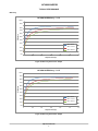
1
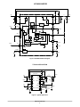
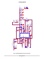
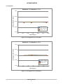
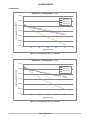
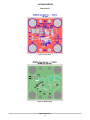
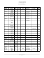
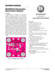
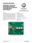
NCV890104GEVB
NCV890104 Evaluation
Board User'sManual
Description
The NCV890104 is a fixed-frequency, monolithic, Buck
switching
regulator
intended
for
Automotive,
battery-connected applications that must operate with up to
a 36 V input supply. The regulator is suitable for systems
with low noise and small form factor requirements often
encountered in automotive driver information systems. The
NCV890104 is capable of converting the typical 4.5 V to
18 V automotive input voltage range to outputs as low as
3.3 V at a constant switching frequency above the sensitive
AM band, eliminating the need for costly filters and EMI
countermeasures. A Reset pin signals when the output is in
regulation, and a pin is provided to adjust the delay before
the RSTB signal goes high. The NCV890104 also provides
several protection features expected in Automotive power
supply systems such as current limit, short circuit protection,
and thermal shutdown. In addition, the high switching
frequency produces low output voltage ripple even when
using small inductor values and an all-ceramic output filter
capacitor − forming a space-efficient switching regulator
solution.
http://onsemi.com
EVAL BOARD USER’S MANUAL
Key Features
•
•
•
•
•
•
•
•
•
•
•
•
•
•
•
•
•
•
Internal N-channel Power Switch
Low VIN Operation Down to 4.5 V
High VIN Operation to 36 V
Withstands Load Dump to 40 V
2 MHz Free-running Switching Frequency
Adjustable Spread Spectrum
Reset with Adjustable Delay
Logic level Enable Input Can be Directly Tied to
Battery
1.4 A (min) Cycle-by-Cycle Peak Current Limit
Short Circuit Protection enhanced by Frequency
Foldback
±1.75% Output Voltage Tolerance
Output Voltage Adjustable Down to 0.8 V
1.4 Millisecond Internal Soft-Start
Thermal Shutdown (TSD)
Low Shutdown Current
NCV Prefix for Automotive and Other Applications
Requiring Unique Site and Control Change
Requirements; AEC−Q100 Qualified and PPAP
Capable
Wettable Flanks DFN (Pin Edge Plating)
These Devices are Pb-Free and are RoHS Compliant
Typical Applications
• Audio, Infotainment, Safety – Vision Systems,
Instrumentation
Figure 1. NCV890104 Evaluation Board
© Semiconductor Components Industries, LLC, 2014
May, 2014 − Rev. 1
1
Publication Order Number:
EVBUM2230/D
NCV890104GEVB
CDRV
VIN
VIN
DBST
SW
L1
3V
Reg
CBST
DFW
DRV
BST
Oscillator
RSTB
PWM
LOGIC
ON OFF
RSTB
DELAY
CDELAY
+
+
−
Reset
Delay
FB
+
−
+
GND
COMP
Clamp
TSD
+
Soft−Start
RESET
COMP
Voltages
Monitors
+
−
Enable
VOUT
EN
RCOMP
+
CCOMP
RMOD
RDEPTH
Spread
Spectrum
RDEPTH
RMOD
Figure 2. NCV890104 Block Diagram
TYPICAL APPLICATION
CDRV
DBST
NCV890104
L1
VOUT
VIN
1 VIN
SW 12
2 DRV
BST 11
CIN
CBST
DFW
RSTB
3 RSTB
COUT
RFB1
DELAY 10
CDELAY
4 GND
FB 9
EN
5 EN
COMP 8
RFB2
RCOMP
6 RDEPTH RMOD 7
CCOMP
RDEPTH
RMOD
Figure 3. Typical Application
http://onsemi.com
2
COUT
NCV890104GEVB
Table 1. EVALUATION BOARD TERMINALS
Pin Name
Function
VIN
Positive dc Input Voltage
GND
Common dc Return
VOUT
Positive dc Output Voltage
EN
RST3B
Master Enable Input
Reset with Adjustable Delay
Table 2. ABSOLUTE MAXIMUM RATINGS (Voltages are with respect to GND)
Rating
Dc Supply Voltage (VIN, EN)
Dc Supply Voltage (RSTB)
Storage Temperature Range
Value
Unit
−0.3 to 40
V
−0.3 to 6
V
−55 to +150
°C
Stresses exceeding those listed in the Maximum Ratings table may damage the device. If any of these limits are exceeded, device functionality
should not be assumed, damage may occur and reliability may be affected.
Table 3. ELECTRICAL CHARACTERSITICS
Characteristic
Conditions
Typical Value
Unit
5.0
V
REGULATION
Output Voltage (VOUT)
Line Regulation (VOUT)
IOUT = 1.0 A
0.1
%
Load Regulation (VOUT)
VIN = 13.2 V
0.1
%
Switching Frequency
2.0
MHz
Soft-start Time
1.4
ms
EN = 5 V
2.35
A
VIN Decreasing
3.4
V
TJ Rising
170
°C
SWITCHING
CURRENT LIMIT
Peak Current Limit (VOUT)
PROTECTIONS
Input Undervoltage Lockout (UVLO)
Thermal Shutdown
Product parametric performance is indicated in the Electrical Characteristics for the listed test conditions, unless otherwise noted. Product
performance may not be indicated by the Electrical Characteristics if operated under different conditions.
http://onsemi.com
3
VIN
L2
4.7uH
GND
RDEP
EN
KLV1 is shorted with
copper in the PCB layout.
10K
0603
DEV_GNDRRDEP
RDEP
EN
KLV1
10K
0603
RRSTB
GND
VOUT
GND
RSTB
1
RSTB
NCV890104
DRV
6
5
4
3
RDEPTH
EN
GND
RESET
FB
8 COMP
9
10 DLY
FB
0.47uF 0603
DLY
DBST
BST BAS16HT1G
CDLY
DEV_GND
CBST
0.1uF
0603
CDRV
0.1uF
0603
10V/X7R
SW
4.7uH
DFW
MBRS1540T3G
XAL4030−472
Figure 4. NCV890104GEVB Evaluation Board Schematic
DEV_GND
0603
C0G / 50V
RFB2
31.6
0603
RFB1
100
0603
Coilcraft XAL4030−472ME
L1
CSNB
OPEN
0603
10V/X7R
RSNB
OPEN
0603
ZFB1
COMP 4.7nF
0603
RCOMP
50V
7 RMODRRMOD DEV_GND 6.98k
RMOD
0603
10K
0603
CCOMP
RMOD
330pF
COMP
FB
DELAY
1
12 SW
VIN
SW
CVIN2
NCV890104
1uF
2
11 BST
0805
BST
DRV
50V/X7R
CFLT2
4.7uF
1210
50V/X7R
VIN
CVIN1
4.7uF
1210
50V/X7R
M_PD_IND
CFLT1
4.7uF
1210
50V/X7R
VSUP
GND
4
2
http://onsemi.com
13
Coilcraft XAL7030−472ME
COUT1
10uF
1206
X7R/10V
COUT2
10uF
1206
X7R/10V
VOUT
RMIN1
OPEN
1206
RMIN2
OPEN
1206
GND
GND
GND
VOUT
NCV890104GEVB
NCV890104GEVB
OPERATIONAL GUIDELINES
1. Connect a dc input voltage, within the 6.0 V to
36 V range, between VIN and GND.
2. Connect a dc enable voltage, within the 2.0 V to
36 V range, between EN and GND. This will
power up the switcher. The VOUT signal should
be 3.3 V.
3. Add a load to VOUT – up to 1.0 A.
Figure 5. NCV890104 Board Connections
ADDITIONAL GUIDELINES
Output Voltage Selection
Some common setups are listed below:
The voltage output for the switcher is adjustable and can
be set with a resistor divider. The FB reference for the
switcher is 0.8 V.
Desired
Output (V)
VREF (V)
RUPPER
(kW, 1%)
RLOWER
(kW, 1%)
1.2
0.8
5.11
10.0
1.5
0.8
8.87
10.0
1.8
0.8
12.7
10.0
2.5
0.8
21.5
10.0
3.3
0.8
31.6
10.0
5.0
0.8
52.3
10.0
VOUT
RUPPER
FB = 0.8 V
Spread Spectrum
In SMPS devices, switching translates to higher
efficiency. Unfortunately, the switching leads to a much
noisier EMI profile. We can greatly decrease some of the
radiated emissions with some spread spectrum techniques.
Spread spectrum is used to reduce the peak electromagnetic
emissions of a switching regulator.
RLOWER
Use the following equation:
R UPPER + R LOWER
V OUT*V FB
V FB
http://onsemi.com
5
NCV890104GEVB
Time Domain
The modulation depth and modulation frequency are each
set by an external resistor to GND. The modulation
frequency can be set from 5 kHz up to 50 kHz using
a resistor from the RMOD pin to GND. The modulation
depth can be set from 3% up to 30% of the nominal switching
frequency using a resistor from the RDEPTH pin to GND.
Please see the curves below for typical values:
Frequency Domain
Unmodulated
V
52
fc
3fc
5fc
7fc
9fc
MODULATION FREQUENCY (kHz)
t
V
t
fc
3fc
5fc
7fc 9fc
The spread spectrum used in the NCV890104 is an
“up-spread” technique, meaning the switching frequency is
spread upward from the 2.0 MHz base frequency. For
example, a 5 % spread means that the switching frequency
is swept (spread) from 2.0 MHz up to 2.1 MHz in a linear
fashion – this is called the modulation depth. The rate at
which this spread takes place is called the modulation
frequency. For example, a 10 kHz modulation frequency
means that the frequency is swept from 2.0 MHz to 2.1 MHz
in 50 ms and then back down from 2.1 MHz to 2.0 MHz in
50 ms.
47
42
37
32
27
22
17
12
7
2
0
10
20
30
RMOD, (kW)
40
50
60
Figure 6. Modulation Frequency vs. RMOD Value
MODULATION DEPTH (%FSW)
35
30
25
20
15
10
5
0
0
10
20
30
RDEPTH, (kW)
40
50
60
Figure 7. Modulation Depth vs. RDEPTH Value
Spread spectrum is automatically turned off when there is
a short to GND or an open circuit on either the RMOD pin
or the RDEPTH pin. Please be sure that the ROSC pin is an
open circuit when using spread spectrum.
http://onsemi.com
6
NCV890104GEVB
TYPICAL PERFORMANCE
Efficiency
NCV890104 Efficiency − 3.3 V
100%
90%
80%
Efficiency
70%
60%
50%
40%
30%
VIN = 6.0 V
VIN = 13.2 V
20%
VIN = 28.0 V
10%
0%
0
0.2
0.4
0.6
0.8
1.0
1.2
Output Current (A)
Figure 8. Efficiency with a 3.3 V Output
NCV890104 Efficiency − 5.0 V
100%
90%
80%
Efficiency
70%
60%
50%
40%
30%
VIN = 6.0 V
20%
VIN = 13.2 V
VIN = 28.0 V
10%
0%
0
0.2
0.4
0.6
0.8
Output Current (A)
Figure 9. Efficiency with a 5.0 V Output
http://onsemi.com
7
1.0
1.2
NCV890104GEVB
Line Regulation
NCV890104 − Line Regulation − 3.3 V
Line Regulation (% of VOUT)
1.00%
0.50%
0.00%
−0.50%
IOUT = 100 mA
IOUT = 500 mA
IOUT = 1.0 A
−1.00%
0.00
5.00
10.00
15.00
20.00
25.00
30.00
Input Voltage (V)
Figure 10. Line Regulation for a 3.3 V Output
NCV890104 − Line Regulation − 5.0 V
Line Regulation (% of VOUT)
1.00%
0.50%
0.00%
−0.50%
IOUT = 100 mA
IOUT = 500 mA
IOUT = 1.0 A
−1.00%
0.00
5.00
10.00
15.00
20.00
Input Voltage (V)
Figure 11. Line Regulation for a 5.0 V Output
http://onsemi.com
8
25.00
30.00
NCV890104GEVB
Load Regulation
NCV890104 − Load Regulation − 3.3 V
0.04%
VIN = 6.0 V
Load Regulation (% of VOUT)
0.02%
VIN = 13.2 V
VIN = 28.0 V
0.00%
−0.02%
−0.04%
−0.06%
−0.08%
0
0.2
0.4
0.6
0.8
1.0
1.2
Output Current (A)
Figure 12. Load Regulation with a 3.3 V Output
NCV890104 − Load Regulation − 5.0 V
0.02%
VIN = 6.0 V
Load Regulation (% of VOUT)
0.00%
VIN = 13.2 V
VIN = 28.0 V
−0.02%
−0.04%
−0.06%
−0.08%
−0.10%
0
0.2
0.4
0.6
0.8
Output Current (A)
Figure 13. Load Regulation with a 5.0 V Output
http://onsemi.com
9
1.0
1.2
VIN
L2
4.7uH
GND
RDEP
EN
KLV1 is shorted with
copper in the PCB layout.
10K
0603
DEV_GNDRRDEP
RDEP
EN
10K
0603
RRSTB
KLV1
VOUT
GND
RSTB
GND
RSTB
NCV890104
DRV
6
5
4
3
RDEPTH
EN
GND
RESET
FB
8 COMP
9
10 DLY
FB
0.47uF 0603
DLY
DBST
BST BAS16HT1G
CDLY
DEV_GND
CBST
0.1uF
0603
CDRV
0.1uF
0603
10V/X7R
SW
4.7uH
DFW
MBRS1540T3G
XAL4030−472
DEV_GND
0603
C0G / 50V
RFB2
31.6
0603
RFB1
100
0603
Coilcraft XAL4030−472ME
L1
CSNB
OPEN
0603
10V/X7R
RSNB
OPEN
0603
ZFB1
COMP 4.7nF
0603
RCOMP
50V
7 RMODRRMOD DEV_GND 6.98k
RMOD
0603
10K
0603
CCOMP
RMOD
330pF
COMP
FB
DELAY
1
12 SW
VIN
SW
CVIN2
NCV890104
1uF
2
11 BST
0805
BST
DRV
50V/X7R
CFLT2
4.7uF
1210
50V/X7R
VIN
CVIN1
4.7uF
1210
50V/X7R
M_PD_IND
CFLT1
4.7uF
1210
50V/X7R
VSUP
GND
10
1
http://onsemi.com
2
Figure 14. Schematic
13
Coilcraft XAL7030−472ME
COUT1
10uF
1206
X7R/10V
COUT2
10uF
1206
X7R/10V
VOUT
RMIN1
OPEN
1206
RMIN2
OPEN
1206
GND
GND
GND
VOUT
NCV890104GEVB
SCHEMATIC
NCV890104GEVB
PCB LAYOUT
Figure 15. Top View
Figure 16. Bottom View
http://onsemi.com
11
NCV890104GEVB
BILL OF MATERIALS
Table 4. BILL OF MATERIALS
Manufacturer
Manufacturer’s
Part Number
Substitution
Allowed
Kemet
C0603C104K8RACTU
Yes
603
Murata Electronics
North America
GCM1885C1H331JA16D
Yes
10%
603
Murata Electronics
North America
GCM188R71E474KA64D
Yes
4.7 mF
10%
1210
Murata Electronics
North America
GRM32ER71H475KA88L
Yes
CAP CER
10 mF 10 V X7R
1206
10 mF
10%
1206
Murata Electronics
North America
GRM31CR71A106KA01L
Yes
1
CAP CER
1.0 mF 50 V
X5R 0805
1.0 mF
10%
805
Murata Electronics
North America
UMK212BJ105KG-T
Yes
DBST
1
DIODE
SWITCH
200 mA 75 V
SOD323
75 V/0.2 A
N/A
SOD_323
ON Semiconductor
BAS16HT1G
No
DFW
1
DIODE
SCHOTTKY
1.5 A 40 V SMB
40 V/1.5 A
N/A
SMB_DIODE
ON Semiconductor
MBRS1540T1G
No
L1
1
INDUCTOR
POWER 4.7 mH
4.5 A SMD
4.7 mH
4.5A
XAL4030-472
Coilcraft
XAL4030-472ME
No
L2*
1
RES 0.0 W
1/4 W JUMP
1206 SMD
0W
5%
1206
Yageo
RC1206JR-070RL
Yes
RCOMP
1
RES 6.98 kW
1/10 W 1%
0603 SMD
6.98 kW
1%
603
Vishay/Dale
CRCW06036K98FKEA
Yes
RFB1
1
RES 100 W
1/10 W 1%
0603 SMD
100 W
1%
603
Vishay/Dale
CRCW0603100RFKEA
Yes
RFB2
1
RES 31.6 W
1/10W 1% 0603
SMD
31.6 W
1%
603
Vishay/Dale
CRCW060331R6FKEA
Yes
RRDEP,
RRMOD,
RRSTB
3
RES 10.0 kW
1/10 W 1%
0603 SMD
10.0 kW
1%
603
Vishay/Dale
CRCW060310K0FKEA
Yes
ZFB1
1
CAP CER
4700 pF 50 V
10% X7R 0603
4,700 pF
10%
603
Murata Electronics
North America
GRM188R71H472KA01D
Yes
CSNB
1
Do Not
Populate
603
Yes
RMIN1,
RMIN2
2
Do Not
Populate
1206
Yes
RSNB
1
Do Not
Populate
603
Yes
BST, COMP,
DLY, FB,
RDEP, RMOD,
SW
7
CIRCUIT PIN
PRNTD .020″D
.425″L
Do Not
Populate
N/A
TPA
Mill-Max
Manufacturing
Corp.
3128-2-00-15-00-00-08-0
Yes
GND1, GND2,
VIN, VOUT
4
CONN JACK
BANANA
UNINS PANEL
MOU
N/A
N/A
BANANA
Emerson Network
Power Connectivity
Soultions
108-0740-001
Yes
Reference
Designator(s)
Qty.
Description
Value
Tolerance
Footprint
CBST, CDRV
2
CAP .10 mF
10 V CERAMIC
X7R 0603
0.1 mF
10%
603
CCOMP
1
CAP CER
330 pF 50 V
C0G 0603
330 pF
10%
CDLY
1
CAP CER
0.47 mF 25 V
10% X7R 0603
0.47 mF
CFLT1,
CFLT2, CVIN1
3
CAP CER
4.7 mF 50 V
10% X7R 1210
COUT1,
COUT2
2
CVIN2
http://onsemi.com
12
NCV890104GEVB
Table 4. BILL OF MATERIALS (continued)
Manufacturer’s
Part Number
Substitution
Allowed
Mill-Max
Manufacturing
Corp.
2501-2-00-44-00-00-07-0
Yes
TP
Vector Electronics
K24C/M
Yes
12PINDFN4×4p65
ON Semiconductor
NCV890104MWR2G
No
Reference
Designator(s)
Qty.
Description
Value
Tolerance
Footprint
Manufacturer
GND3−GND6
4
TERM
SOLDER
TURRET .219″
.109″L
N/A
N/A
TURRET
EN, RSTB
2
PIN INBOARD
.042″ HOLE
1000/PKG
N/A
N/A
NCV890104
1
1.2 A 2 MHz
Automotive
Buck Switching
Regulator
NCV890104
N/A
*L2 is a placeholder footprint for an optional input inductor filter component. Boards are shipped with a shorting jumper installed to complete
the input path.
NOTE: All devices are RoHS Compliant.
ON Semiconductor and
are registered trademarks of Semiconductor Components Industries, LLC (SCILLC). SCILLC owns the rights to a number of patents, trademarks,
copyrights, trade secrets, and other intellectual property. A listing of SCILLC’s product/patent coverage may be accessed at www.onsemi.com/site/pdf/Patent−Marking.pdf. SCILLC
reserves the right to make changes without further notice to any products herein. SCILLC makes no warranty, representation or guarantee regarding the suitability of its products for any
particular purpose, nor does SCILLC assume any liability arising out of the application or use of any product or circuit, and specifically disclaims any and all liability, including without
limitation special, consequential or incidental damages. “Typical” parameters which may be provided in SCILLC data sheets and/or specifications can and do vary in different applications
and actual performance may vary over time. All operating parameters, including “Typicals” must be validated for each customer application by customer’s technical experts. SCILLC
does not convey any license under its patent rights nor the rights of others. SCILLC products are not designed, intended, or authorized for use as components in systems intended for
surgical implant into the body, or other applications intended to support or sustain life, or for any other application in which the failure of the SCILLC product could create a situation where
personal injury or death may occur. Should Buyer purchase or use SCILLC products for any such unintended or unauthorized application, Buyer shall indemnify and hold SCILLC and
its officers, employees, subsidiaries, affiliates, and distributors harmless against all claims, costs, damages, and expenses, and reasonable attorney fees arising out of, directly or indirectly,
any claim of personal injury or death associated with such unintended or unauthorized use, even if such claim alleges that SCILLC was negligent regarding the design or manufacture
of the part. SCILLC is an Equal Opportunity/Affirmative Action Employer. This literature is subject to all applicable copyright laws and is not for resale in any manner.
PUBLICATION ORDERING INFORMATION
LITERATURE FULFILLMENT:
Literature Distribution Center for ON Semiconductor
P.O. Box 5163, Denver, Colorado 80217 USA
Phone: 303−675−2175 or 800−344−3860 Toll Free USA/Canada
Fax: 303−675−2176 or 800−344−3867 Toll Free USA/Canada
Email: [email protected]
N. American Technical Support: 800−282−9855 Toll Free
USA/Canada
Europe, Middle East and Africa Technical Support:
Phone: 421 33 790 2910
Japan Customer Focus Center
Phone: 81−3−5817−1050
http://onsemi.com
13
ON Semiconductor Website: www.onsemi.com
Order Literature: http://www.onsemi.com/orderlit
For additional information, please contact your local
Sales Representative
EVBUM2230/D