1
TECHNICAL MANUAL
OPERATION AND MAINTENANCE INSTRUCTIONS
LASER CEILOMETER CTl2K
VAISALA
100 COMMERCE WAY
WOBURN, MA 01801
PART NO. 66-2292
COPYRIGHT © VAISALA 1986,1987,1988,1989.
ALL RIGHTS RESERVED.
This publication contains proprietary information and may not be
reproduced in any form without prior written permission of VAISALA.
The contents of instruction manuals are subject to change without
a prior notice.
SAFETY SUMMARY
The following general safety precautions must be observed during all phases of
operation, service, and repair of this instrument. Failure to comply with these
precautions, or with specific warnings elsewhere in this manual violates safety standards
of design, manufacture, and intended use of the instrument. VAISALA assumes no
liability for the customer’s failure to comply with these requirements:
NEVER LOOK INTO LASER TRANSMITTER WITH MAGNIFYING OPTICS: The
instrument is intended for operation in an area restricted from public access, and pointing
vertically up. Whenever this is not the case, care must be observed so as to prevent
exposure to the laser beam through focusing optics. Work area access by unauthorized
persons during service operations must be prevented.
GROUND ‘THE INSTRUMENT:
To minimize shock hazard, the instrument chassis and
cabinet must be connected to an electrical ground. The instrument is equipped with a
three-conductor AC power connector. The power cable must either be plugged into an
approved tlhree-contact electrical outlet or the instrument must be carefully earthed to
a low-resistance safety ground.
DO NOT OPERATE IN AN EXPLOSIVE ATMOSPHERE: Do not operate the
instrument in the presence of flammable gases or fumes. Operation of any electrical
instrument in such an environment constitutes a definite safety hazard.
KEEP AWAY FROM LIVE CIRCUITS: Operating personnel must not remove
instrument covers. Component replacement and internal adjustments must be made by
qualified maintenance personnel. Do not replace components with power cable
connected. Under certain conditions, dangerous voltages may exist even with the power
cable removed. To avoid injuries, always disconnect power and discharge circuits before
touching them.
DO NOT SERVICE OR ADJUST ALONE: Do not attempt internal service or
adjustment unless another person, capable of rendering first aid and resuscitation, is
present.
DO NOT SUBSTITUTE PARTS OR MODIFY INSTRUMENT: Because of the danger
of introducing additional hazards, do not install substitute parts or perform any
unauthorized modification to the instrument. Return the instrument to a VAISALA
office or authorized Depot for service and repair to ensure that safety features are
maintained.
DANGEROUS PROCEDURE WARNINGS: Warnings, such as the example below,
precede potentially dangerous procedures throughout this manual. Instructions contained
in the warnings must be followed:
WARNING! Dangerous voltages, capable of causing death, are present in this
instrument. Use extreme caution when handling, testing, and adjusting.
i
ii
ii
AMENDMENTS TO
CEILOMETER CT-12K TECHNICAL MANUAL (REVISION E - SEPT. 1989)
AMENDMENT
NUMBER
NEW
REVISION
AMENDMENT DESCRIPTION OR
PARAGRAPHS AFFECTED
...
iii
111
NEW
SOFTWARE
DATE
EFFECTIVE
Please note that the following pages without text or diagrams were intentionally left
blank:
ii, x, 2, 12, 13, 14, 16, 28, 29, 30, 34, 91, 92, 116, 118, 212, 222, 224, 256, 257, 258, 260,
263, 264, 266, 302, 303, 304
iv
TECHNICAL MANUAL
LASER CElLOMETER CT12K
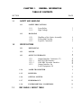
TABLE OF CONTENTS
CHAPTER
CHAPTER
CHAPTER
CHAPTER
PAGE
*..i
Safety Summary
Amendments to this Manual
Table of Contents
List of Drawings and Illustrations
List of Tables
vii
ix
1.
GENERAL INFORMATION
1
1.1
1.2
1.3
Safety and Handling
Specifications
RBC Angle / Height Table
11
2.
INSTALLATION
15
2.1
2.2
2.3
2.4
2.5
General
Site Preparation
Start of Operation
Performance Verification
Drawings
17
18
20
23
24
3.
OPERATION
31
3.1
3.2
3.3
3.4
3.5
General
Standard Outputs
Parameters and Operation Modes
Performance Monitoring and Alarms
Operation with Maintenance
Terminal CTH 12
35
44
61
67
4.
FUNCTIONAL DESCRIPTION
93
4.1
4.2
4.3
Operation Principles
Technical Description
Module Descriptions
v
111
V
z
82
97
102
128
259
CHAPTER 5.
5.1
5.2
5.3
CHAPTER 6.
6.1
6.2
6.3
6.4
Monthly Check of Message Alarms
90 Day Check of Window Cleanliness
and Cleaning Procedure
Monthly Check of
Window Conditioner Blower
TROUBLESHOOTlNG AND REPAIR
Diagnosis
Verification and Replacement
Removal of Ceilometer Covers
Offset Calibration
vi
261
261
262
265
267
282
299
300
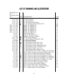
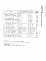
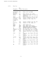
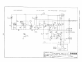
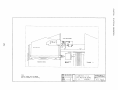
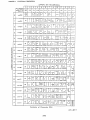
DRAWING NO.
OR
ILLUSTRATION
REV
NO.
FIG
FIG
FIG
FIG
FIG
FIG
U.CT 3445
U.CT 3282
C . C T 3105
A.CT 3406
1 CT 4569
2 CT 4570
3 CT 4571
4 CT 4572
5 CT 4573
6 CT 4574
CT 4413
CT 4411
CT 4412
U.CT 1104
U.CT
.CT 2101
CT 2295
A.CT 3400
A.CT 3401
A.CT 3402
A.CT 3403
A.CT 3404
A.CT 3405
A C T 3406
A.CT 4407
CT 4532
CT 3501
CT 3385
CT 3386
CT 3387
CT 3388
CT 3544
C.CT 2492
CT 3536
CT 3196
C.CT 2294
CT 2277
C
C
B
.a
;
A
i3
B
B
B
B
A
A
8”
A
D
A
C
B
C
E
B
PAGE
DESCRIPTION
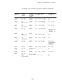
CT 12K Ceilometer
CT 12K Installation
CT 12K Connection Diagram
CT 12K Equipment Base, Bottom View
RMOD On, BMOD Off
RMOD On, BMOD Off
RMOD On, BMOD Off
RMOD On, BMOD On
RMOD Off, BMOD Off
RMOD Off, BMOD On
Actual Return Signal
Diagram of Internal Cycles
Diagram of Recorder Outputs
CT 12K Wiring Diagram
CT 12K Generation Breakdown Chart
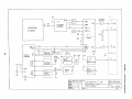
CT 12K Block Diagram
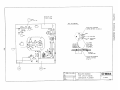
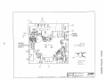
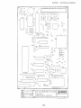
CT 12K General Layout
CT 12K Internal Layout, Front View
CT 12K Internal Layout, Rear View
CT 12K Internal Layout, Right Hand View
CT 12K Internal Layout, Left Hand View
CT 12K Internal Layout, Top View
CT 12K Equipment Base, Bottom View
CT 12K Processor Board CTM 12 Jumpers & Connectors
CTM 12 Main Functions and Primary Data/Control Flow
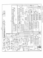
CTM 12 Processor Board Principle Block Diagram
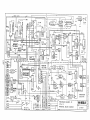
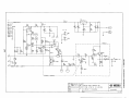
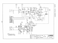
CTM 12 Processor Board Circuit Diagram l/4 (CPU)
CTM 12 Processor Board Circuit Diagram 2/4 (Monitor)
CTM 12 Processor Board Circuit Diagram 3/4 (Seq.Cont)
CTM 12 Processor Board Circuit Diagram 4/4 (Amp)
CTM 12 Processor Board CPU Cycle Timing
CTM 12 Processor Board Component Layout
CTM 12 Processor Board Pulse Diagram
CTS 12 Unreg. Power Sup. Circuit Diagram
CTS 12 Unreg. Power Sup. Components Layout
CTI 12 Output Interface Circuit Diagram
vii
24
25
26
z::
58
59
60
60
60
97
107
112
117
119
120
121
122
123
124
125
126
127
157
158
159
160
161
162
163
164
165
166
173
174
183
DRAWING NO.
OR
ILLUSTRATION
NO.
C.CT 3278
CT 3564
U.CT 3560
A.CT 3410
CT 3593
C.CT 3596
CT 4594
CT 4417
CT 3120
C.CT 2210
CT 3289
U.CT 1200
C.CT 3207
CT 4290
U.CT 1300
U.CT 2311
A.CT 3416
CT 2284
C.CT 3493
PAGE
DESCRIPTION
CTI 12 Output Interface Components Layout
CTL 13 Light Monitor Board Circuit Diagram
CTL 13 Light Monitor Board Components Layout
CT 12K Light Monitor Board CTL 13 Assembly
CTR 13 Receiver Board Circuit Diagram
CTR 13 Receiver Board Components Layout
Typ.Temp. Dependence of MRHV
Laser Diode Temp. Curve/TP3 Volt. Curve Form
CTT 12 Transmitter Board Circuit Diagram
CTT 12 Transmitter Board Components Layout
CTP 12 HVPS Circuit Diagram
C T P 12 HVPS Wiring Diagram
CTP 12 HVPS Components Layout
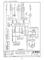
Window Conditioner Bl Connection Diagram
CT 12K Heater Sub-Assembly
CT 12K Blower Sub-Assembly
CTH 12 Maintenance Terminal Block Diagram
CTH 12 Maintenance Terminal Circuit Diagram
CTH 12 Maintenance Terminal Component Layout
...
viii
vlll
184
190
191
192
199
200
201
206
210
211
220
221
223
229
230
231
253
254
255
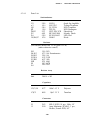
LIST OF TABLES
NUMBER
CT 3415
CT 4577
PAGE
DESCRIPTION
Monitored Parameters
Contents of Character ROM
ix
90
242
x
x
CHAPTER 1.
GENERAL INFORMATION
TABLE OF CONTENTS
SECTION
1.1
PAGE
SAFETY AND HANDLING
1.1.1
SAFETY PRECAUTIONS
1.1.1.1
1.1.1.2
1.1.2
Handling of the Optics Assembly
Lifting and Carrying
Exposed Connectors
4
4
4
SPECIFICATIONS
1.2.1
MECHANICAL
5
1.2.2
POWER
5
1.2.3
OUTPUT INTERFACES
1.2.3.1
1.2.3.1.1
1.2.3.1.2
1.2.3.2
1.3
3
3
HANDLING
1.1.2.1
1.1.2.2
1.1.2.3
1.2
Laser Safety
High Voltage
Output Interface Connector (J3)
Bell 103 FSK Interface
Gifft RBC Recorder Interface
Output Interface for
Local Equipment (54)
1.2.4
LASER TRANSMITTER
8
1.2.5
RECEIVER
9
1.2.6
OPTICAL SYSTEM
10
1.2.7
PERFORMANCE
10
1.2.8
ENVIRONMENTAL CONDITIONS
10
RBC ANGLE / HEIGHT TABLE
1
11
2
CHAPTER 1.
GENERAL INFORMATION
1.1 SAFETY AND HANDLING
1.1.1 SAFETY PRECAUTIONS
1.1.1.1 Laser Safety
The CT-12K laser ceilometer is classified as a Class 1 laser device when used
within its normal operational conditions. This means that a CT-12K Laser
Ceilometer installed in a field environment with instrument covers on poses
no established biological hazard to humans. However, the following precautions
are to be noted and followed during service and maintenance of the
instrument:
The CT-12K uses invisible laser radiation which may harm human eyes.
Never look directly into the transmitter with magnifying glasses, binoculars,
telescopes, etc.
When operating, avoid looking at the unit from the beam direction.
Only trained personnel should perform maintenance functions.
Follow all WARNING!-labels.
WARNING!-label used with CT-12K:
DANGERINVISIBLE LASER RADIATION
WHEN OPEN.
AVOID DIRECT EXPOSURE
TO BEAM.
NON-INTERLOCKED
PROTECTIVE
HOUSING
WARNING LABEL.
1.1.1.2 High Voltage
High voltage will be readily accessible when the transmitter (A7) or receiver
(A6) covers are removed and the unit is powered. High voltage is present in
the High Voltage Power Supply (PS1) and Window Conditioner (Bl).
WARNING!-labels used with CT-12K:
DANGERHIGH VOLTAGE INSIDE
THIS COVER
RECEIVER (A6) AND
TRANSMITTER (A7)
COVER WARNING LABELS
DANGERHIGH VOLTAGE INSIDE
THIS ENCLOSURE
HIGH VOLTAGE
POWER SUPPLY (PSl)
WARNING LABELS
3
CHAPTER 1.
GENERAL INFORMATION
1.1.2 HANDLING
1.1.2.1
Handling of the Optics Assembly
The VAISALA cloud ceilometer CT-12K uses laser radiation, produced by a
GaAs semiconductor diode, for detecting cloud levels.
The laser radiation is accurately collimated by internal optics and provides a
beam of 904 nm invisible laser light. During the factory alignment procedure,
the optical adjustments are carefully carried out to fulfil1 the requirements and
specifications of the device. Optical adjustments occur at factory or depot
only. There is no need to readjust any of these settings at the field site
before installation. If mishandling occurs during transit or installation, the
instrument should be returned to a VAISALA office or authorized Depot for
inspection.
Do not touch the lens surfaces. Maintain dust covers on the lenses during
adjustments and during long periods of storage.
The optics and windows should always be kept clean of any dirt or particles,
especially during operation.
1.1.2.2 Lifting and Carrying
Do not attempt to carry the unit alone. Do not lift the unit from Window
Conditioner or Equipment Cover; lift from Equipment Base only. Use proper
gloves for protection against sharp edges, etc. Disconnect Window Conditioner
Cable from Equipment Base before placing unit on flat, hard surface. Remove
cable from underneath Equipment Base edge.
1.1.2.3 Exposed Connectors
Maintain dust caps on all external connectors if stored unpacked for extended
times in an unconditioned area. When installed, always maintain the integral
protective caps on the unused interface connector (J3 or J4) and the
Maintenance Terminal CTH12 connector.
4
CHAPTER 1. GENERAL INFORMATION
1.2 SPECIFICATIONS
1.2.1 MECHANICAL
Height: Total . . . . . 52.8 in. (1340 mm)
Excluding Pedestal . . 29.1 in. ( 740 mm)
Width . . . . . . . . . . . 22.8 in. ( 580 mm)
Depth . . . . . . . . . . . 16.5 in. ( 420 mm)
Weight: Total . . . 156 Lbs. (71 kg)
Excluding
Pedestal 135 Lbs. (61 kg)
1.2.2 POWER
800 W (7 A) max.
45 Hz to 65 Hz
115 V ± 10%
220 / 240 V (optional)
Power connector (Jl): MIL-C-26482 type MS 3110E12-3P (male)
Mating connector type: MS 3116F12-3S or equivalent
1.2.3 OUTPUT INTERFACES
1.2.3.1 Output Interface Connector (J3)
MIL-C-26482 type MS 3112E12-8P (male)
Mating connector type: MS 3116F12-8S or equivalent
Circuit A-B: FSK Interface
Circuit C-D: Recorder Trigger Break
Circuit E-F: Recorder Inscription (Cloud) Signal
Circuit G:
Equipment Ground
All signal circuits are non-polar, symmetrical; electrically floating to overvoltage
protection rating (300V-500V).
Overvoltage Protection in each circuit:
Primary. . . . ..Noble Gas Surge Arrester
Secondary....Wirewound Resistors and Transient Zeners or Diodes
5
CHAPTER 1. GENERAL INFORMATION
1.2.3.1.1 Bell 103 FSK Interface
Bell 103 standard Frequency Shift Keyed (FSK)
Full Duplex Modem Interface for
Serial Asynchronous Data Interchange
Baud Rate: 300
Answer Mode Standard Frequencies: Mark (1) 2225 Hz
Space (0) 2025 Hz
Originate Mode Optional
-6 dBm (0.3 V) into 600 Ohm standard
0, -3, -6, -9, -21 dBm optional
Signal Level:
(Jumper-Selectable)
Distance to
Operate:
0...l0 miles (0...16 km)
with AWG 22 (0.35 mm2),
unshielded twisted pair
Standard Character Frame: 1 start bit
8 data bits
No Parity
1 stop bit
Standard Character Code:
USASCII
8th (unused) data bit MARK (1)
1.2.3.1.2 Gifft RBC Recorder Interface
Trigger Break Relay Contact; N/C
Ratings: 150 VDC max
2 A max
107 cycles at 24 VDC, 1A Resistive
Break Duration:
80 ms normally
200 ms for Fault Indication
Inscription (Cloud) Signal:
Transformer Coupled, 600 ohms standard
Signal level ON:
+2 dBm standard
Jumper selectable:
-2, 0, +2, +5 dBm
Frequency: 2 x Line Frequency
(normally 2 x 60 Hz = 120 Hz)
6
CHAPTER 1.
GENERAL INFORMATION
Signals Interrelationship:
End of Trigger Break starts timing of delay to Cloud Signal;
3 seconds (= max) delay equals 12,000 ft;
linear delay-to-height relationship,
Distance to Operate::
0...l0 miles (16 km) with AWG 22 (0.35 mm2)
unshielded twisted pair terminated by recorder
Field Junction Box
1.2.3.2
Output Interface for Local Equipment (J4)
RS-232C standard serial asynchronous full duplex input/output interface,
internally parallelled with FSK interface.
Used also with Ceilometer Maintenance Terminal.
Ceilometer configured as Data Terminal Equipment (DTE).
Baud Rate:
Note!
300 Baud standard and default
1200 Baud available on command
FSK interface operates at 300 Baud only
Distance to Operate: 1000 ft (300 m) at 300 Baud
300 ft (100 m) at 1200 Baud
(typical values with standard
communication cables)
Overvoltage Protection:
Series resistors and Transient Zeners
Connector (54): MILC-26482 type MS3110E12-8S (female)
Mating connector: MS 3116F12-8P or equivalent
Circuits: B
C
F
A
H
G
TXD Transmitted Data (from Ceilometer)
RXD Received Data (from external equipment)
Signal Ground
Equipment Ground
+ 12 V DC supply (for Maintenance Terminal CTH 12)
Flag (from Maintenance Terminal CTH 12)
7
CHAPTER 1.
GENERAL INFORMATION
1.2.4 LASER TRANSMITTER
Laser Source:
Gallium Arsenide (GaAs) Semiconductor Diode
Wavelength:
904 nm nominal
Operating Mode:
Pulsed
Initial
Transmitted
Pulse Energy:
Peak Pulse Power:
Pulse Width, 50%:
6.6 µWs ± 5% (factory adjustment)
40 W typical
135 ns typical
Repetition Rate:
620 Hz-1120 Hz, processor controlled for
constant average power
Average Power:
5 mW
Max b-radiance:
Laser
Classification:
50 µW/cm² measured with Dia. 7 mm aperture
Class 1 in compliance with
FDA CFR 1040.10 (Subsection e,3)
Laser Source
Dimensions:
50 mil square (1.3 mm x 1.3 mm)
Transmitter
Optics System
Focal Length:
14.45 inches (367 mm)
Transmitter
Effective Lens
Diameter:
4.65 inches (118 mm)
Transmitter
Beam
Divergence:
±2.5 mrad maximum
Lens
Transmittance:
9 0 % typical
Window
Transmittance:
97% typical, clean
8
CHAPTER 1.
1.2.5 RECEIVER
Detector:
Silicon Avalanche Photodiode
Responsivity at 904 nm:40 A/W
(factory adjustment)
Surface Diameter:
0.0314 inches (0.8 mm)
Interference Filter:
904 nm
50% Pass Band:
880-940 nm typical
Transmissivity
at 904 nm:
85% typical
60% minimum
Focal Length:
5.91 inches (150 mm)
Receiver Lens
Effective Diameter:
4.65 inches (118 mm)
Field-of-View
Divergence:
±2.7 mrad
Lens
Transmittance:
90% typical
Window
Transmittance:
97% typical, clean
9
GENERAL INFORMATION
CHAPTER 1. GENERAL INFORMATION
1.2.6 OPTICAL SYSTEM
Lens Distance Transmitter-Receiver:
Laser Beam Entering Receiver
12.20 inches (310 mm)
Field-of-View:
l00
Laser Beam 90% Within
Receiver Field-of-View:
1000
feet (30 m)
feet (300 m)
1.2.7 PERFORMANCE
Measurement Range:
0 - 12,650 feet
Resolution:
50 feet
12,000 ft Acquisition Time:
30 s maximum
System Bandwidth:
10 MHz at Low Gain (-3db)
3 MHz at High Gain (-3db)
Tolerance
to Precipitation:
to 0.3 inches per hour
(7.5 mm per hour) range limited
1.2.8 ENVIRONMENTAL CONDITIONS
-60°F... + 120°F
Ambient Temperature:
(-51°C... + 49°C)
Humidity:
100% RH
Salt Spray:
MIL-STD-810C
MILSTD-810C Method 509.1
Wind:
100 kt
Shock:
4-inch drop (10 cm)
10
(50 m/s)
CHAPTER 1.
1.3
GENERAL INFORMATION
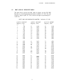
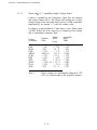
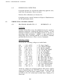
RBC ANGLE / HEIGHT TABLE
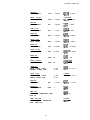
The table below converts the RBC angle in degrees on the Gifft RBC
Recorder to a cloud height determined by the VAISALA CT-12K. The scale
is linear, 1 degree equals 133.3 feet, with 0 to 90 degrees representing 0 to
12,000 feet.
GIFFT RBC RECORDER/CEILOMETER VAISALA CT-12K
ANGLE HEIGHT
(degrees) (feet)
A N G L E HEIGHT
(degrees) (feet)
ANGLE HEIGHT
(degrees) (feet)
0
0
1
130
2
270
3
400
4
530
5
670
6
800
7
930
8
1070
9
1200
10
1330
31
32
33
34
35
36
37
38
39
40
4130
4270
4400
4530
4670
4800
4930
5070
5200
5330
61
62
63
64
65
66
67
68
69
70
8130
8270
8400
8530
8670
8800
8930
9070
9200
9330
11
12
13
14
15
16
17
18
19
20
1470
1600
1730
1870
2000
2130
2270
2400
2530
2670
41
42
43
44
45
46
47
48
29
50
5470
5600
5730
5870
6000
6130
6270
6400
6530
6670
71
72
73
74
75
76
77
78
79
80
9470
9600
9730
9870
10000
10130
10270
10400
10530
10670
21
22
23
24
25
26
27
28
29
:;
30
2800
2930
3070
3200
3330
3470
3600
3730
3870
4000
51
52
53
54
55
56
57
58
59
60
6800
6930
7070
7200
7330
7470
7600
7730
7870
8000
81
82
83
84
85
86
87
88
89
90
10800
10930
11070
11200
11330
11470
11600
11730
11870
12000
11
12
13
14
CHAPTER 2.
INSTALLATION
TABLE OF CONTENTS
SECTION
2.1
PAGE
GENERAL
2.1.1
2.16
2.1.3
2.1.4
2.2
PREFACE
TRANSPORTATION CONTAINER
ORIENTATION
REQUIREMENTS
SITE PREPARATION
2.2.1
2.2.2
2.2.3
2.3
20
20
20
LINE POWER “ON”
INTERFACES
MAINTENANCE TERMINAL CTH 12
21
21
23
PERFORMANCE VERIFICATION
2.4.1
2.4.2
2.5
FOUNDATION
CABLING
GROUNDING
START OF OPERATION
2.3.1
2.3.2
2.3.3
2.4
19
19
19
19
MESSAGE ALARMS
OPERATIONAL CHECK WITH TOTAL COMMAND
23
23
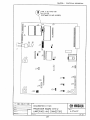
DRAWINGS
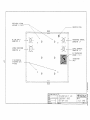
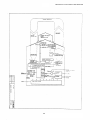
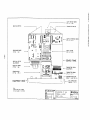
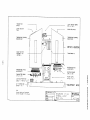
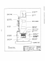
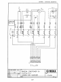
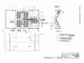
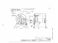
CT 12K CEILOMETER
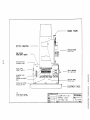
CT 12K INSTALLATION
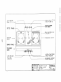
CONNECTION DIAGRAM
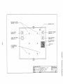
EQUIPMENT BASE, BOTTOM VIEW
15
(U.CT 3445)
(U.CT 3282)
(A.CT 3105)
(A.CT 3406)
24
25
26
27
16
16
CHAPTER
2.1
2.
INSTALLATION
GENERAL
2.1.1
PREFACE
The installation of laser cloud ceilometer CT 12K requires a
concrete foundation and a set of cables to establish the operation.
Some basic information is needed to guarantee the proper start-up
of the instrument. It is important to carefully follow the
installation instructions.
2.1.2
TRANSPORTATION CONTAINERS
The CT 12K is shipped in two containers, the larger one
containing the Ceilometer without Pedestal, and the smaller one
containing Pedestal, Maintenance Terminal CTH 12, Field Site
Spares Kit, and installation accessories.
The main container is provided with unpacking and re-packing
instructions which are to be observed.
Containers are suggested to be saved for eventual later transport
use. Repacking instructions must be carefully observed in that
case since the heavy Main Equipment Assembly may otherwise
be damaged during transport.
2.1.3
ORIENTATION
The receiver side of CT 12K should preferrably be oriented away
from sun (e.g., in the northern hemisphere towards the north
and towards the south in the southern hemisphere). This will
reduce noise of sunlight.
2.1.4
REQUIREMENTS
For mechanical installation requirements, refer to Installation
Drawing U.CT 3282.
For electrical connections, refer to Connection Diagram C.CT
3105.
Suggested Cable Dimensions
Line AC Supply Cable:
Standard 3-pronged power cord
3 x min 0.75 mm² (AWG 18)
RS-232C Interface:
(subset of Maintenance
Terminal Interface)
22 Gage Stranded conductors twisted
pair with foil shield and drain
wire.
17
CHAPTER 2.
INSTALLATION
Output Interface Cable
22 Gage stranded conductors 3
(Twisted Pairs Preferred)
twisted pairs with foil shield
and drain wire. Minimum working
voltage 200 volts.
Window Conditioner Cable: 6 x min 0.75 mm² (AWG 18)
(Part of Window Conditioner,
supplied)
Maintenance Terminal
Cable:
(Part of Maintenance
Terminal, supplied)
2.2
8 x 0.75 mm² (AWG 18)
SITE PREPARATION
2.2.1
FOUNDATION
The suggested minimum dimensions for the foundation are found
in Installation Drawing U.CT 3282.
Mounting hardware is included with the Pedestal.
If a new foundation is laid, the Wedge Bolts and Foundation
Screws (4 each), are suggested to be cast into the concrete so
that 1 to 2 inches (25 to 50 mm) of the threads stand above the
surface.
If an existing foundation is used, four holes of Diameter 0.5
inches x 6.5 inches (12 mm x 165 mm) are drilled into the
concrete. The Wedge Bolt and Foundation Screw combinations
are placed in the holes, with Wedge Bolts down; the protruding
threads are alternately hammered and tightened a few times so
that the Wedge Bolts attach to the hole walls.
18
CHAPTER 2. INSTALLATION
2.2.2
CABLING
All the cable connectors are located under the equipment base
and are referred to as Jl, J2, J3, and J4.
The location of the connectors are found in Bottom View
Drawing ACT 3406.
The connector signals and connector types are found in the
Connection Diagram C.CT 3105.
Mating connectors for Jl (Power) and J3 (Output Interface) are
supplied with the Ceilometer.
2.2.3
GROUNDING
The power supply connector Jl provides a standard protective
ground for the instrument chassis.
Connection of an external earthing shall be made to the ground
terminal of the equipment base (reference: A.CT 3406 for
location).
CONNECTION TO A SOLID EARTH GROUND AT THE
INSTALLATION SITE IS MANDATORY FOR ADEQUATE
LIGHTNING AND TRANSIENT PROTECTION.
19
CHAPTER 2.
2.3
INSTALLATION
START OF OPERATION
2.3.1
LINE POWER “ON”
Before plugging in any connectors, check the field cables referred
to in the Connection Diagram C.CT 3105.
Remove the unit covers of CT 12K and make a visual check of
the internal connectors, subassemblies, etc.
Turn the main circuit breaker CBl to “OFF” position.
Plug in the line supply cable to connector Jl after checking the
voltage and signals of the power supply cable connector.
The line voltage indicator DSl in PSl should be lit indicating
the line voltage at the main circuit breaker CBl.
When turning the main circuit breaker CBl to the “ON” position,
the following shall happen with the monitoring LEDs D4 and D5
on the processor board, Al:
D4 (red) “ON” for approximately 5 seconds (internal
reset performed).
D5 (green) After D4 has turned “OFF”, this will
start blinking at a rate of once per second (software
operates normally)
If LEDs D4 and D5 operate differently, the unit
needs service or maintenance. Refer to Chapter 6,
‘Troubleshooting”.
20
CHAPTER 2. INSTALLATION
2.3.2
INTERFACES
The CT 12K provides three (3) different interfaces for remote
devices:
0
0
0
RS-232C Maintenance Terminal Interface
Bell 103 Modem Interface
Gifft RBC Recorder Interface
Depending on the distance between the Ceilometer and the
observer site, the data communication can be arranged either with
the RS-232C level direct connection (up to 1000 feet) or with the
Bell 103 modem connection (for distances exceeding 1000 feet).
The RS-232C (Maintenance Terminal) connection signals are
available at CT 12K equipment base connector J4.
The Gifft RBC Recorder interface consists of two (2) signal pairs:
0
0
Recorder sweep synchronization (trigger break)
Cloud Data signal
The modem signals and Gifft RBC Recorder signals are available
through connector J3. Reference Connection Diagram C.CT
3105.
The CTI 12 Interface Board (Reference A3) provides five LEDs
for monitoring the communication:
0
D10
(yellow) TXD (Transmitted Data) Indicates
a presence of data being transmitted from
the processor board Al, either via the
modem circuitry or via the RS-232C
0
Dll
(yellow) RXD (Received Data) Data
received via the modem line
0
Dl2
(green) CD (Carrier Detect) Indicates the
presence of a carrier in the receive channel
of the modem communication
0
D13
(yellow) RBCT (RBC-recorder Trigger
Break) Gifft RBC Recorder pen sweep start
and synchronization signal
0
D14
(yellow) RBCE (RBC-recorder Enable
Cloud Signal) Gifft RBC Recorder cloud
data signal
21
CHAPTER 2. INSTALLATION
These LEDs provide an easy means to check and monitor the
operation of the communication.
After “POWER UP”, the following sequence is performed
automatically ‘by the CT 12K software:
0
Data transmission starts with the data memory and
modem test messages, and "TXD" will blink
according to the character stream.
0
The modem circuitry and communication lines, if
used, are tested and the communication is
established. “CD” will be turned on for 2 - 3
seconds while the testing is performed, then remains
“OFF” except when an active counter-modem with
carrier “ON” is connected to J3.
0
Modem test, program memory tests and internal
status messages are transmitted and "TXD" will
indicate the presence of transmission.
In the normal operation mode (Automatic mode) the cloud data
collection and the calculations take maximum of 30 seconds to
provide the first message table. When the message is sent, "TXD"
will indicate the character stream of transmission for serial
communications (RS-232C or Modem).
The Gifft RBC Recorder output LEDs D13, and D14 shall start
operating according to the interface specifications in 12 seconds.
However, the automatic measurements of the Ceilometer may be
terminated for maintenance purposes by using the AUTO OFF
command. Refer to Chapter 3, “Operation.” In the maintenance
mode, most of the functions can be individually activated and,
therefore, easily tested.
After monitoring the operation with the LEDs on Al and A3,
the cables can be connected to the connectors J3 and J4.
The operation should continue as described earlier. If not, then
the cables, operators’ terminals, etc., should be checked and
possible mistakes corrected.
2.3.3
MAINTENANCE TERMINAL CTH 12
While operating at the installation site, the Maintenance Terminal
CTH 12 provides an easy way to monitor and control the
operation of the Ceilometer. Refer to Chapter 3.
The Maintenance Terminal is connected to connector J4 of the
equipment base.
22
CHAPTER 2. INSTALLATION
2.4
PERFORMANCE VERIFICATION
2.4.1
MESSAGE ALARMS
Check that the Start-Up Message (Reference Paragraph 3.4.3)
does not contain any messages of alarm, error or suspicion, and
that none of the numerical values output in the message has an
asterisk ("*") immediately after it.
After Start-Up, observe operation for a suitable time. Check that
no alarms are generated.
If cause for suspicion exists, turn to Chapter 6 .
2.4.2
OPERATIONAL CHECK WITH TOTAL COMMAND
The CT 12K Ceilometers are factory adjusted and aligned for
optimum performance.
After installation, the operation can be checked with a constant
and solid cloud base within the height range of 1000 - 5000 ft
with no fog, haze or precipitation. The TOTAL command of the
CT 12K software is used for this purpose.
To use the TOTAL command, proceed as follows:
0
Open the communication line giving a “CR” symbol
(CR = Carriage Return from the Operator’s
Terminal)
0
Give “TOTAL” command and “CR”
The CT 12K software responds to this by giving the parameter
value (TOTAL SIGNAL LIMIT) and the measured total value
(CURRENT SIGNAL SUM).
The “SUM” values reported in above conditions should be in
range 20...40. If out of limits, then turn to Chapter 6.
For exact command syntaxes and additional information, see
Section 3.4.
23
28
29
30
CHAPTER 3. OPERATION
TABLE OF CONTENTS
SECTION
3.1
PAGE
GENERAL
3.1.1
3.1.2
3.1.3
INTRODUCTION: NORMAL, OPERATION
SWITCHES
INDICATORS
3.1.4
USE OF SERIAL DIGITAL INTERFACE
3.1.4.1
3.1.4.2
3.1.4.3
3.1.4.4
3.1.4.5
3.1.4.6
3.2
General
Frame, Code and Speed
Notations and Abbreviations
Line Closed - Line Open
Command Format and Editing Rules
Advanced Information
35
35
36
37
37
38
39
40
41
3.1.5
AUTOMATIC MODE - MAINTENANCE MODE
41
3.1.6
FAST HEATER OFF
43
STANDARD OUTPUTS
36.1
DIGITAL MESSAGE NO. 2
3.2.1.1
3.2.1.2
3.2.1.3
3.2.1.4
3.2.1.5
3.2.1.6
3.2.2
General
Format
Status Line 1
Status Line 2
Data Line Format
Message Example
44
44
45
46
47
49
DIGITAL MESSAGE NO. 3
3.2.2.1
3.2.2.2
3.2.2.3
3.2.2.4
3.2.2.5
General
Format
Status Line 1
Backscatter Data Line
Message Example
31
50
50
51
51
51
3.23
GIFFT RBC RECORDER OUTPUT
3.2.3.1
3.2.3.2
3.2.3.3
3.2.3.4
3.3
52
52
53
55
PARAMATERS AND OPERATION MODES
3.3.1
3.3.2
3.4
Introduction
Signals
Recording Modes and Set-Up
Commands
Examples and Interpretation
STANDARD PARAMETER SETTINGS
DESCRIPTION OF PARAMETERS
61
62
PERFORMANCE MONITORING AND ALARMS
3.4.1
3.4.2
3.4.3
3.4.4
GENERAL
STATUS MESSAGE
START-UP
ALARM LIMITS
3.4.5
COMMANDS FOR DETAILED CHECKING
3.4.5.1
3.4.5.2
3.4.5.3
3.4.5.4
3.4.5.5
3.4.5.6
3.4.5.7
3.4.5.8
3.4.5.9
3.4.5.10
3.4.5.11
3.4.5.12
3.4.5.13
3.4.5.14
3.4.5.15
3.4.5.16
3.4.5.17
3.4.5.18
3.4.5.19
LASE
SEQ
NOIS
FREQ
GAIN
HEAT
BLOW
SHUT
RECT
TIME
DATE
RESE
CAL
HELP
MEAS
TAB
GRAP
MES
32
67
67
68
69
70
71
71
72
72
73
74
74
74
75
75
76
76
77
78
79
79
80
81
3.5
OPERATION WITH MAINTENANCE TERMINAL CTH 12
3.5.1
3.5.2
GENERAL
OPERATION
3.5.2.1
3.5.2.2
3.5.2.3
3.5.2.4
3.5.3
82
83
Opening and Closing the Line
Command Format
Viewing Messages
Operating Session
COMMANDS TABLE
APPENDIX 1: CTM 12 MONITORED PARAMETERS (CT 3415)
33
83
84
85
86
87
90
34
CHAPTER 3. OPERATION
3.1
GENERAL
3.1.1
INTRODUCTION: NORMAL OPERATION
The normal operation of Ceilometer CT 12K is fully automatic
and no intervention is needed.
A digital data message is sent at predetermined intervals, without
any polling action, over both the FSK Interface and the RS-232C
Interface. Framing, content and timing are identical. See paragraph 3.2 for use and interpretation of Digital Messages.
The Gifft RBC Recorder signals are operated at 12 second
intervals. See paragraph 3.2.3 for use and interpretation of these.
The requirements for obtaining normal operation are, along with
the corresponding paragraphs of description in brackets:
Power On and all switches in correct positions (3.1.2,
3.1.3)
Automatic Mode of Operation (3.1.5)
Line Closed (3.1.4)
Correct parameters inserted (3.3)
No alarms detected (3.4)
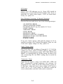
3.1.2
SWITCHES
The following are the switches of Ceilometer CT 12K, along with
Reference Designation and normal operation position:
Position
Ref.
Description
PSl CBl
Power On/Off (doubles as
Circuit Protecting Breaker)
on (up)
PSl CB2
Window Conditioner On/Off
(doubles as Circuit Protecting
Breaker)
on (up)
Al Sl
Reset/Normal /(spare)
Normal
(middle)
A2 Sl
Internal Heating On( = automatic)/Off
On
(right)
A2 S2
Interface Control Normal/Line
Normal
(left)
35
CHAPTER 3.
OPERATION
3.1.3
INDICATORS
The following is a summary of all Ceilometer CT 12K indicators,
with reference designations and indications in normal operation:
Description
Normal Operation
PSI DSl Red
Line Power
Always ON
Al D4 Red
Processor Selfcheck Alarm
Always OFF
Ref.
Color
A l D5 G r e e n Processor OK
Blinking once per second
A 3 Dl0 Ye1
Data Transmitted
on FSK line
Blinking when Ceilometer
transmits digital characters; ON in between
A 3 Dll Ye1
Data Received
on FSK line
Blinking when Ceilometer
receives digital characters; ON in between
A3 D12 Green Carrier Detect
on FSK line
ON when Ceilometer detects
carrier received on
digital FSK line
A3 D13 Ye1
Trigger Break
for Gifft RBC
Recorder
ON when Ceilometer
activates Break
A3 D14 Ye1
Cloud Signal
for Gifft RBC
Recorder
ON when Ceilometer
marks recording paper
A5 D4 Red
Laser Power
Always ON except if
optional Solar Shutter
is ON
36
CHAPTER 3. OPERATION
3.1.4
USE OF SERIAL DIGITAL INTERFACE
3.1.4.1
General
The serial digital interface of Ceilometer CT 12K may be
accessed remotely through the FSK line (connector J3) or locally
- up to a few hundred yards or meters - through the RS-232C
port (connector J4). These are functionally equivalent.
Maintenance Terminal CTH 12 connects to the RS-232C port.
Its presence will convert ceilometer communication to the
Maintenance Terminal mode when the line is opened.
3.1.4.2
Frame, Code and Speed
Communication is asynchronous, 300 Baud, using the following
character frame:
Start Bit
8 Data Bits
No Parity
1 Stop Bit
Character code is USASCII and the unused eighth bit equals the
stop bit in polarity (“MARK”), except for a few special characters
which initialize Maintenance Terminal CTH 12 when it is plugged
in.
37
CHAPTER 3.
OPERATION
3.1.4.3
Notations and Abbreviations
The following notations are used throughout Chapter 3 of this
Manual:
ST:
Standard Terminal or equivalent device
communicating in USASCII
MT:
Maintenance Terminal CTH 12
(CR)
“Carriage Return” i.e. “Return” i.e. “Enter”;
terminates a line; completes and actuates a
command; opens a “closed” line for dialog.
MT: Character F (“Feed”).
ABC
Operator action i.e. input to Ceilometer is
underlined in this description; output from
ceilometer is not.
-
>
CAPITALS
Space character. One or more spaces must
separate different parts of a command.
MT: Character B.
Command Prompt is output by Ceilometer every
time a command has been carried out and a
new one may be input. Maintenance Terminal
(MT) will leave the last line of the previous
command on display until the first character of
the new command is input; this clears the
display.
Ceilometer does not distinguish between letter
cases. Output will be in capitals only.
Y
Yes; equals "1" with MT
N
No; equals "0" with MT
Hex
Hexadecimal code i.e. 0...9 = 0...9 decimal;
A...F = 10...15 decimal.
38
CHAPTER 3. OPERATION
3.1.4.4
Line Closed - Line Open
The serial digital interface serves both for transmitting
measurement data and for communicating e.g. maintenance
information. For separation, the interface has two distinct states:
LINE CLOSED: Normal operation. Measurement data messages
are transmitted
automatically
if in ’
AUTOMATIC MODE of operation (see 3.1.5).
331.5)..
Commands are ignored except for OPEN and
FAST HEATER OFF. This is also Restart and
Power Up default state.
LINE OPEN:
Dialog mode. Commands are accepted and
responded to. Command Prompt arrowhead
bracket (>) signifies readiness. State is not
maintained through a Restart or Power Down.
The state of operation is changed by the OPEN and CLOSE
commands. OPEN is accomplished with a Carriage Return (CR)
only. Command syntaxes and Ceilometer responses are:
ST:
MT:
LINE OPENED FOR
OPERATOR COMMANDS
> -LINE OPEN
> (ready for command input)
(ready for input)
> CLOS(CR)
> ClF
LINE CLOSED
LINE CLOSED
(message output continues)
(output continues)
The LINE OPEN state is automatically terminated in the
Automatic Mode by a one minute time-out after the last character
input.
The Line may be commanded OPEN in the middle of a message
transmission.
Message is not interrupted but response to
command is delayed until the end of message transmission.
In the LINE OPEN mode the last Digital Message No. 2 can be
requested with command MES; see Section 3.4.
39
CHAPTER 3. OPERATION
3.1.4.5
Command Format and Editing Rules
The command consists of a command identifier (ID) and none,
one, two, three or four groups of parameters (PARn). It is
terminated by a Carriage Return (CR) which also actuates its
execution. One or more spaces must separate identifier and
parameters:
ID_PARl_PAR2(CR)
With input commands, new data values or states of operation are
defined by the parameter (one only). If the parameter is omitted,
the current value or state will he output; with certain output commands, a default set of parameters will be used.
With standard ASCII communication (ST:) the identifier part consists of 2 to 4 letters. Additional letters will be ignored. The
pararneters are numbers or letter combinations.
The
DEL(RUBOUT) key can be used for editing the command.
With Maintenance Terminal Communication (MT:) the identifier
part consists of letter C and a number code; these need not be
separated by space. The parameters are numbers, ON and YES
is “1”; OFF and NO is " 0 " No DEL(RUBOUT) equivalent is
available.
Numeric parameters may be input as they are written i.e. zeroes
and decimal point are used as in writing.
All input characters are echoed.
40
CHAPTER 3. OPERATION
3.1.4.6
Advanced Information
Internally, Ceilometer CT 12K is equipped with one serial digital
interface. This is used both for FSK and RS-232C electrical interface ports. Outputs are identical; inputs are ORed. Input devices
may be simultaneously connected to RS-232C and FSK ports but
may not input characters simultaneously.
No handshake signals are used.
The RS-232C port (J4) doubles as a port for Maintenance
Terminal CTH 12.
The presence of this special 16-key,
16-character terminal is sensed by an input signal (‘FLAG”),
whereupon an opening of the line will convert data interchange
to be in the Maintenance Terminal mode.
Output from Ceilometer may be stopped by issuing an XOFF
( =Control- S = 13 hexadecimal). Output will commence upon
reception of any character except XOFF. The BEL character is
output in addition to that shown in this chapter:
when Line is Opened or Closed
when a Syntax Error is encountered
All input parameters and operation modes are stored in
non-volatile memory (EEPROM) except when specifically
mentioned.
3.1.5
AUTOMATIC MODE - MAINTENANCE MODE
The Automatic Mode is the normal mode of operation; the
Maintenance Mode is available for e.g. maintenance checking etc.
The following is a summary of their operations:
AUTOMATIC
MODE
Normal mode of operation. A measurement
cycle is (completed every 12 seconds. Outputs
according to 3.2 are active. The Digital
message is withheld if the line is “opened” for
operator dialog. Internal monitoring and controls
are updated every 15 seconds.
41
CHAPTER 3.
OPERATION
MAINTENANCE Used temporarily for checking operation etc.
Measurement cycle is halted but may be
MODE
operated by command. Measurement calculations are not performed. Internal settings and
controls may be operated by commands.
No automatic time-out for closing an open
communication line is applied.
The Maintenance Mode doubles as a
STANDBY MODE for minimizing wearout of
The Window
laser and moving parts.
Conditioner is operated automatically only the
first 5 minutes every hour of the internal clock.
The following are the commands for setting the mode of
Omitting the
operation, along with Ceilometer response.
parameter part (OFF/ ON or 0/l) results in response according
to the prevailing mode:
ST:
MT:
> AUTO OFF(CR)
> CllB0F
WAIT FOR SEQUENCE STOP
WAIT SEQ. STOP_
MAINTENANCE MODE
>MAINT. MODE
> (next input)
(next input)
> AUTO ON(CR)
> CllBlF
AUTOMATIC MODE
> AUTOMATIC MODE
> (next input)
(next input)
The current 12 second measurement sequence is completed before
switching to Maintenance Mode.
The Mode selection will remain in effect over a Restart or
Powerdown.
42
CHAPTER 3. OPERATION
3.1.6
FAST HEATER OFF
The 600W Window Conditioner Heater can be forced OFF at any
time, e.g. to decrease the loading of an Uninterruptible Power
Supply System.
The OFF state is set via the FSK or KS-232C serial line, by
sending two subsequent BELL characters (= Control-G = 07 Hex)
to the Ceilometer. After reception of the last bit of the two
incoming characters, the Heater will be disconnected within a
maximum of 20 milliseconds.
The state is stored in EEPROM and will thus be preserved over
a power outage or Reset. Status Bit Sl0 of the Digital Messages
(see 3.2) is set to 1 to indicate the forced OFF state. No other
acknowledgement will be output.
The forced OFF state is inhibited. via the FSK or RS-232C serial
line by sending two subsequent ACK characters (= Control-F =
06 hex) to the Ceilometer. After this, the normal control will
resume operation and the heater may be turned on within 15
seconds.
Syntaxes:
ST:
MT:
(BEL) (BEL) (= Cntr-G Cntr-G)
(no equivalent)
(Window Conditioner Heater shuts
OFF within 20 ms.)
(Next digital message status
BIT Sl0=l)
(ACK) (ACK) (= Cntr-F Cntr-F)
(no equivalent)
(Window Conditioner Heater is released to be turned ON if other
conditions call for it)
(Next digital message status
BIT Sl0 = 0)
43
CHAPTER 3 . OPERATION
3.2
STANDARD OUTPUTS
3.2.1
DIGITAL MESSAGE NO. 2
3.2.1.1
General
This message contains detailed range gate data, and internal
monitoring data for the most important variables. Message is
output automatically every 30 seconds in Automatic Mode when
line is closed.
Activation is done with command SEND 2. This cancels any
previous message activation; only one digital message may be
active at a time. The following is the command, and Ceilometer
response; omitting the parameter (2) will cause the current
selected message to be announced:
ST:
MT:
> SEND 2(CR)
> C31B2F
AUTOMATIC MESSAGE: 2
AUTO MES 2
> (next input)
>_ (next input)
The Message number selection will remain in effect over a
Restart or Power-down.
Message can be output with command MES; see Section 3.4.
3.2.1.2
Format
STXCRLF
<status data line l> CR LF
<status data line 2> CR LF
<data table . . .
CR LF
.
CR LF
>
ETX CR LF .*’
ON/OFF data is l/O accordingly.
Other data is decimal or hexadecimal numbers.
44
CHAPTER 3. OPERATION
Coding is USASCII. STX, CR, LF, ETX are Start-of-Text,
Carriage Return Line Feed and End-of-Text characters which
format the message but are not visible in a printout.
Total length of message is 636 characters.
Printout is 15 lines, width is max 44 characters, whereof 42 are
visible.
3.2.1.3
Status Line 1 (Identical in all messages)
NSB-H,H,H,H,H,-T,T,T,T,T,-H 2222t2222tl2345678910
H H H H T T T T T S S S S S S S S S S CRLF
N
N
N
N
=
=
=
=
0 no significant backscatter (clear air)
1 one layer detected
2 two layers detected
3 sky is fully obscured but no cloud base can be detected
from echo signal received (e.g. fog or precipitation)
N = 4 sky is partially obscured and no cloud base is detected
S=1
no alarm status bits Sl...S4 ON for more than 5 mm.
at least one alarm status Sl...S4 ON for more than 5
min.
B =
space if S = 0
B =
‘bel’ character if S = 1. Because 'bel' is a nonprinting
character the alarming line appears one character
shorter in a printout than normally.
S=0
N = 0 or 4: H,=H,=T,=T,= /////
N = 1 or 2: H,H,H,H,H, =
T,T,T,TIT1 =
45
the lowest detected cloud
height in 5 digits. Leading
zeroes not suppressed.
range of backscatter of first
layer; ///// if not defined
CHAPTER 3.
OPERATION
N = 2:
N = 3:
STATUS
s, =
s, =
s, =
s, =
s, =
s, =
S7 =
s, =
s, =
S 10 =
3.2.1.4
H*H,H,H*H, =
second cloud height; /////
if not defined
T,T,T,T,T, =
range of backscatter of
second layer; ///// if not
defined
H,H,H,H,H, =
calculated vertical visibility
TIT,T,T,T1 =
signal range i.e. height of
highest detected backscatter
INDICATORS:
Hardware alarm
Supply Voltage alarm
Laser power low
Temperature alarm
Solar shutter On
Blower On
Heater On
0: Unit is feet
1: Unit is meters
0: Data in internal table 2 is range and instrument
normalized
1: Data in internal table 2 is inverted i.e. extinction normalized
Fast Heater Off is active
Status Line 2
G- F -N.NN_SUM_IIN_LAS_TLx_OF.FS_XX_PP
CR LF
G = 0
G = 2
Gain used is 250
Gain used is 930
F=0
Laser pulse frequency used is 620 Hz (minimum)
F = 7
Laser pulse frequency is 1120 Hz (maximum)
46
CHAPTER 3.
OPERATION
N.NN = Noise RMS voltage in units of ADC increments,
computed from the latest 12 s measurement period.
One digit, two decimals.
SUM = Sum of total backscattered power per unit solid angle
i.e. range and instrument normalization applied. Three
digits, no decimals. Leading zeroes replaced by space
characters.
IIN =
Algorithm related internal processing information. 3
digits.
LASE = Measured Laser Power in units of ADC increments
(LLAS). 3 digits.
TL.x =
Internal variable indicating transmitter temperature. 2
digits, one decimal; preceded by minus sign if negative.
Degrees Celsius.
OF.FS = Offset of zero signal relative to Data Table minimum
(=0), in units of ADC increments. Two digits, two
decimals.
3.2.1.5
XX=
algorithm related internal processing information. 2
digits.
PP =
A two digit number representing calculated extinction
coefficient values of the ten lowest range gates
(0...500ft.). This two digit number will determine if the
obscuration is ground based.
Data Line Format
H H D0 D1 D2 D 3 . . . . . . . . D9 CR LF
Data scaled to hexadecimal number O...FE (decimal 0...254).
Overflow indicated by FF. Leading zero replaced by space
character.
Data values are presented for each 50 ft range gate.
Height of the first value in the line in thousands of feet. Two
digits; leading zero replaced by space. Twenty 50 ft values per line
starting with 0 (ft), next line 1000 (ft). 13 lines altogether. Last
line (12000 ft) has 10 values.
47
CHAPTER 3. OPERATION
Compression and Scaling
The data item is compressed and scaled according to the following
formula:
DD = 50 x ln(RAWDATA - MINV) + 1
where
DD
is the data item for a particular range gate,, in 2
digit hexadecimal format
ln
symbolizes the natural logarithm
RAWDATA is the raw data value measured for the range gate
in question
MINV
is the smallest raw data value measured
The raw data value differential is retrieved with the following
formula:
(RAWDATA-MINV)=exp(D$)-1
NOTE:
The data values presented are those of the last complete
12 s scan. The cloud heights etc. presented in Status
Line 1 (ref. paragraph 3.2.1.3) may have been
determined from the two last 12 s scans and minor
inconsistencies may therefore appear in rapidly changing
situations.
(Key: First digit of field XX of Status Line 2, ref. paragraph
3.2.1.4, indicates number of scans used for Status Line 1 cloud
information.)
48
CHAPTER 3. OPERATION
Data Item to Backscatter Power Relationship
Let
S = (RAWDATA-MINV)-Noise
where Noise is the remaining noise-induced offset of the data
table.
Then instantaneous received backscatter power P is:
P = (S*O.lSS
GAIN -1 µW
where GAIN is 250 at No. 0 or 930 at No. 2.
3.2.1.6
Message Example
STXCRLF
10- 04200_00150_/////_/////_0000011010 CR LF
2- 3- 0.08
36 12- 168- 23.9
-,- 4.56- 20- 10 CR LF
ODD . . . . . . . . . . . . . . . . . . . . . . . . . . . . DD CR
-1
CR
-2
CR
-3
CR
-4
CR
-5
CR
‘; (DATA VALUES;) CR
CR
-8
CR
-9
CR
io
CR
11
CR
12DD . . . . . . . . . . . . . . . . . DD CR LF
ETX CR LF
= Space Character
49
LF
LF
LF
LF
LF
LF
LF
LF
LF
LF
LF
LF
CHAPTER 3. OPERATION
3.2.2
DIGITAL MESSAGE NO. 3
3.2.2.1
General
This message contains Status Line 1 identical to Message No. 2
(see 3.2.1.3) and one single range gate data line indicating the
presence or absence of backscatter in each range gate.
Message is output automatically every 12 seconds, simultaneously
with the Gifft RBC Recorder Output (3.3) in Automatic Mode
when Line is Closed.
Activation is done with command SEND 3. This cancels any
previous message activation; only one digital message may be
active at a time. The following is the command and Ceilometer
response; omitting the parameter (3) will cause the current
selected message to be announced:
ST:
MT:
> SEND 3(CR)
> C31B3F
AUTOMATIC MESSAGE: 3
AUTO MES 3
> (next input)
>_ (next input)
The Message number selection will remain in effect over a
Restart or Power-Down.
Message No. 3 is intended to be used with the EMOD control
parameter set to EMOD ON (see 3.3).
3.2.2.2
Format
STX CR LF
<status data line l> CR LF
<backscatter data line . . . > CR LF
ETX CR LF
Status Data Line 1 is identical to that of Message No. 2.
ON/OFF data is l/O accordingly. Other data is decimal or
hexadecimal numbers.
50
CHAPTER 3. OPERATION
Coding is USASCII. STX, CR, LF, ETX are Start-of-Text,
Carriage Return Line Feed and End-of-Text characters which
format the message but are not visible in a printout.
Total length of message is 112 characters. Printout is 2 lines,
width is max. 66 characters, whereof 64 are visible.
Time for message transmission at 300 baud is 3.73 s.
3.2.2.3
Status Line 1
Identical to that of Digital Message No. 2; see 3.2.1.3.
3.2.2.4
Backscatter Data Line
D 1 D 2 D 3 D4 . . . . . . . . . . . . . . . . . . D64CR LF
D”
where n= 1 to 64 is single ASCII coded hexadecimal
character O...F where each bit of the 4-bit nibble of
the hex character expressed in binary form represents
one range gate.
With EMOD ON, range gate bit is 1 if Ceilometer
determined extinction coefficient at that range gate
exceeds a value corresponding to a horizontal visibility
of approx. 10 km (6 miles) except for three lowest range
gates which have higher thresholds.
D, represents the four lowest 50 ft range gates i.e. Oft,
50ft, l00ft, 150ft; D, represents the four next ones i.e.
200 ft, 250ft, 300ft, 350ft, etc.
0 indicates no detectable backscatter in four adjacent
range gates
F indicates backscatter in all four range gates
8 indicates backscatter in the lowest range gate only
1 indicates backscatter in the highest range gate only
All other characters indicate a gate-by-gate combination
of backscatter according to the binary nibble, converted
to hexadecimal.
3.2.2.5
Message Example
STX CR LF
10 04200 00150 ///// /////_0000011010 CR LF
oooiFFF8@@OOO&JOOOO~AOOO . . . . ..OOO CR LF
ETXCRLF
51
CHAPTER 3.
OPERATION
3.2.3
GIFFT RBC RECORDER OUTPUT
3.2.3.1
Introduction
The CT 12K Ceilometer provides two floating non-polar output
signal circuits for producing graphical sky condition records on a
Gifft RBC Recorder, operating according to the facsimile
principle.
A new output is generated once every 12 seconds when the
Ceilometer is in Automatic Mode, regardless of the state of the
Digital Interface (Open or Closed). In normal operation (Line
Closed), output coincides once per minute with Digital Message
No. 2 transmission start, and every time with Digital Message No.
3 transmission start.
3.2.3.2
Signals
TRIGGER BREAK (Ref. RBCT)
Normally-Closed relay contact that opens for 80 milliseconds as
an initiation for a new output.
Doubles as an Alarm Signal by extending the break duration to
200 ms when cause for Ceilorneter Fault Alarm exists. This state
is logically identical to that of bits S and B of Status Line 1 of
Digital Messages.’
CLOUD SIGNAL (Ref. RBCE)
Transformer Coupled 120 Hz, signal (twice Line Frequency), on/
off controlled by Ceilometer for inscribing on Recorder paper.
OPERATION AND TIMING+
The Cloud Signal outputs cloud and obscuration heights as an
analog delay with respect to the trailing edge of the Trigger
Break. 0 to 12,000 ft is covered in 3 seconds, with a 20 ms
resolution equalling 80 ft. If the Trigger Break is 200 ms (alarm)
then the reference starting point is 80 ms after the leading edge
of the Break.
52
CHAPTER 3. OPERATION
3.2.3.3
Recording Modes and Set-Up Commands
Two on/off parameters RMOD and BMOD condition the Cloud
Signal output:
RMOD (Recording MODe)
OFF:
Only Cloud bases are recorded
ON:
In addition to Cloud bases also non-cloud
obscuration is recorded
BMOD (Base MODe)
OFF:
Up to two cloud bases may be output during
one sweep, each with a trace duration of mm.
80 ms.
ON:
Only the lowest cloud base is output, and with
a fixed 60 ms trace duration.
RECOMMENDED STANDARD SETTINGS ARE:
RMOD ON
BMOD OFF
53
CHAPTER 3. OPERATION
Settings Matrix:
RMOD
OFF
ON
None, one, or two
bases recorded
with long traces
None, one or two
bases recorded
with long traces,
non-cloud
obscuration
with short
intermittent dots
None or one base
recorded with
short trace
None or one base
recorded with
short trace,
non-cloud
obscuration
with short
intermittent dots
OFF
BMOD
ON
Syntaxes:
ST:
MT:
> RMOD ON(CR)
> C13BlF
MEASURED DATA RECORDING, > RMOD ON
RMOD ON
> RMOD OFF (CR)
> C13B0F
DETECTED CLOUDS RECORDING,
> RMOD OFF
RMOD OFF
> (next input)
(next input)
> BMOD ON(CR)
> C29BlF
CLOUD BASE ONLY, BMOD ON > BMOD ON
54
CHAPTER 3. OPERATION
> BMOD OFF(CR)
> C29B0F
ALL CLOUD DATA, BMOD OFF
> BMOD OFF
> (next input)
(next input)
Settings are stored in non-volatile memory.
3.2.3.4
Examples and Interpretations
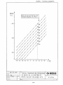
Scaling: The CT 12K 0 t o 12000 ft range is linearly scaled for
the Gifft RBC Recorder 0 to 90 degrees scale i.e.:
= 0 deg
0 ft
1000 ft = 7.5 deg
12000 ft = 90 deg
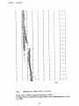
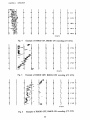
Cloud Trace:
An instantaneous 12 sec. cloud hit is recorded as a
solid thin line starting at the detected cloud height and
extending upwards a minimum of 240 ft (60 ms) and
a maximum equalling the penetration (typ. max. 400 ft).
A time graph of cloud height is produced by several
subsequent instantaneous traces.
In broken, scattered, or highly turbulent conditions instantaneous hit traces may be spread over a wide range,
or group into several distinct cloud mass images. Visual
grouping and averaging of a longer period of the record
will then provide a better result for reporting purposes
than instantaneous hits.
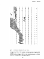
Non-Cloud Obscuration
Height ranges where backscatter has been detected and
the obstruction calculated to have a point extinction
coefficient exceeding a value corresponding to a
horizontal visibility of approx. 6 miles (10 km) but not
exceeding the cloud criteria, are marked with a greyish
cloud signal in the RMOD ON recording mode.
The greyish appearance is accomplished by
semi-randomly on-off switching the cloud signal during
the sweep, and disabling the non-cloud obscuration
signal altogether every second sweep.
55
CHAPTER 3.
OPERATION
In totally obscured conditions where no cloud base is
detected the non-cloud obscuration signal will be output
up to the calculated Vertical Visibility (ceiling) height;
this can then be seen in the record as the upper
(higher) edge of the greyish area.
In cases of rapid changes in cloud heights and/or position, backscatter from a cloud base may be blurred over
a wide range and momentarily fail to produce a reliable
cloud backscatter signature. These instants will however
at least provide a non-cloud obscuration detection to
enhance the record image of the situation.
56
CHAPTER 3. OPERATION
3.3
PARAMETERS AND OPERATlON MODES
3.3.1
STANDARD PARAMETER SETTINGS
Existing parameter settings are checked with commands PAR,
SHUT, SEND, AUTO, SERN. Below is a dialogue session
showing the syntaxes and standard factory settings. If deviations
exist, please check also instrument specific configuration
documents.
Example Dialogue with standard settings:
ST:
MT:
>PAR(C!R)
SYSTEM PARAMETERS
CLOUD LIMIT
0.1000
CLIM
0.2000
SIGNAL LIMIT SLIM
1.2400
DEVICE SCALE DEV
4.5000
NSCA
NOISE SCALE
OUTPUT SCALE SCAL
100 .oooo
LASER NORM
LNOR 164
TOTAL SIGNAL TOTAL 10.0000
3.7012
GAIN RATIO
RAT
>C4F
SYSTEM PARAMETER E
CLIM
0.1000 E
SLIM
0.2000 E
DEV
1.2400 E (5
NSCA
4.5000 E
SCAL 100.0000 z
&NOR
164 E
(5
TOTA
10.0000 E
RAT
3.7012 g
HEIGHT OFFSET HOFF
HOFF
0
HEIGHT SQUARE NORMALIZED MODE,
EMOD OFF
DATA UNIT FT
MEASURED DATA RECORDING,
RMOD ON
ALL CLOUD DATA, BMOD OFF
>SHUT(CR)
NO SHUTTER
0
E
EMOD OFF e
_DATA UNIT FT
_RMOD ON Jf
BMOD OFF E
Tm
>kJO SHUTTER
>SEND(CR)
AUTOMATIC MESSAGE: 2
>AUTO(CR)
AUTOMATIC MODE
>w
AUTO MES 2
%llF
>AUTOMATIC MODE
VAISALA CT 12K VERSION 2.42
SN:87023
By2.42 87023
(next input)
(next input)
61
E
(4
(3
(2
CHAPTER 3.
OPERATION
NOTES:
1. All these parameters reside in non-volatile memory.
2. SEND may be 2 or 3; see Section 3.2.
3. Response to SHUT is SHUTTER IS OFF (or eventually ON)
if one is installed. See also CONF.
4. If meters output is used DATA UNIT FT line will read
DATA UNIT M. See also CONF.
5. LNOR and DEV values are instrument specific.
6. In addition to proper parameter settings, a proper Noise Offset Calibration must be in memory. See Section 6 in case of
doubt.
3.3.2
Description of Parameters
CLIM (Cloud LIMit)
Sets the minimum increase in calculated extinction coefficient
in Ceilometer specific units that must be present over a short
range for cloud base condition. See SLIM for additional
conditions.
SLIM (Signal LIMit)
Sets the minimum calculated extinction coefficient value in
Ceilometer specific units that must be present in one range
gate for cloud base condition.
DEV (DEVice scale)
Multiplying scaling factor applied to all range gate values
after normalization and prior to application of Cloud detection
algorithms and output. Does not affect heights. Does affect
CURRENT SIGNAL SUM, see TOTA.
NSCA (Noise SCAle)
Multiplying scaling factor which when multiplied with the
RMS noise calculated from the 12 sec. measurement scan
sets the limit for discriminating between true signal and noise.
Decreasing NSCA will increase sensitivity but cause more
noise hits.
SCAL (SCALe)
Multiplying scaling factor to scale the value of PP.
LNOR (Laser NORmal power)
Device specific parameter for 100% nominal laser power, in
units of Monitor A/D converter increments. Measured laser
power (LLAS) is compared against this for laser power control
and measurement normalization.
62
CHAPTER
3. OPERATION
TOTA (TOTAl signal sum limit)
Limit for determining full, partial or no obscuration. For
every 12 sec. scan all range and equipment normalized range
gate backscatter values are added to provide value CURRENT
SIGNAL SUM or SUM (see Digital Message No. 2). If SUM
exceeds TOTA then full obscuration is concluded and first
status bit N of Digital Message Status Line 1 is 1, 2 or 3.
If SUM is less than TOTA but exceeds 0.4* TOTA then
partial obscuration is concluded and N is 4. No height values
are output in message. If SUM is less than 0.4* TOTA then
no significant obscuration is detected. Parameter DEV
multiplies SUM.
RAT (RATio)
Ratio of GAIN 2/GAIN 0. Multiplies results of measurement
using GAIN 0 for normalization. Value must always be 3.7.
HOFF (Height OFFset)
Parameter for offsetting the heights reported in case the
Ceilometer is installed considerably higher (positive value)
or lower (negative value) than the level of interest, e.g. the
runway.
The HOFF value will be added to the Cloud Height and
Range Limit values. Cloud Penetration or Vertical Visibility
values will not be affected except that Vertical Visibility will
be set equal to Range Limit if the latter is lower. Negative
values will be replaced by zeroes.
The Height Offset will offset the Range Gate output string
of Digital Message No. 3 correspondingly. Digital Message
No. 2 range gate data and Gifft RBC Outputs will not be
affected.
The HOFF value must be expressed in the same units (feet
or meters) as the output is.
WARNING 1: If output units are changed from feet to
meters or vice versa, the HOFF value must
be changed manually.
No automatic
recalculation is performed.
WARNING 2:
If clouds or obscuration exists beween the
Ceilometer installation height and the level
of interest (e.g. runway), the Ceilometer
output will not be representative of the sky
condition situation at the level of interest.
63
CHAPTER 3.
OPERATION
RMOD (Recording MODe)
Controls the presentation. of non-cloud obstruction of the
Gifft RBC Recorder; output included if ON. See also 3.2.3.
BMOD (Base MODe)
Controls the presentation of a second cloud height, and cloud
penetration in all outputs;, maximum amount of output data
available if OFF. See paragraph 3.2.
EMOD (Extinction MODe)
Controls the availability of extinction normalized (“inverted’)
range gate data with Digital Message No. 3; see Paragraph
3.2. Extinction normalized data available if ON. ON setting
seen as Digital Message Status Line 1 bit S9 = 1.
CONF (CONFiguration)
Determines if the output is feet (F) or meters (M), and tells
the software whether a Solar Shutter is installed (Y) or not
(N). The command is interactive, asking the operator above
questions. No (CR) is needed for input of configuration
parameters. Meters setting seen as Digital Message Status
Line 1 bit S8= 1.
SEND (SEND)
Selects Digital Message No. 2 or 3 for output.
AUTO (AUTOmatic mode)
Sets the ceilometer in Automatic Mode which is the normal
operating mode.
SERN (SERial Number)
Arbitrary serial number ‘option. Range 0 . . . 999999. Only
numericals allowed. Stored in the Processor Board EPROM.
Will thus require reprogramming if Board or EEPROM is
replaced. Has no effect on operation. Changing of number
once input requires string (space) (space) NEW with standard
terminal, or string (space) (space) 123 with Maintenance
Terminal to be added after the new number before entering
line with (CR).
Example session showing syntaxes of above commands:
MT:
ST:
>CLIM(CR)
CLOUD LIMIT
CLIM
0.1600
x6K
>CLIM
-
XLIM .15(CR)
CLOUD LIMIT
CLIM
0.1000
X6BD15F
>CLIM 0.1500
64
0.1600
CHAPTER 3. OPERATION
>SLIMICR)
SIGNAL LIMIT
SLIM
0.2600
XlOF
>SLIM
>SLIM .25(CR)
SIGNAL LIMIT
SLIM
0.2500
>Cl0BD26F
>SLIM 0.2500
>DEV(CR)
DEVICE SCALE
DEV
1.2000
X9F
>@i
>DEV l(CR)
DEVICE SCALE
DEV
1.000
>DEV
>NSCA (CR)
NOISE SCALE
NSCA
2.5000
>w
>&3X4
>NSCA 3(CR)
NOISE SCALE
NSCA
3.0000
>C8B3F
XJSCA 3.0000
>SCAL (CR)
OUTPUT SCALE
SCAL
20.0000
>u
>gziL
>SCAL l0(CR)
OUTPUT SCALE
SCAL
10.000
>C7BlOF
+XL 10.0000
>LNOR (CR)
LASER NORM
LNOR 162
>C28F
>&NOR
>LNOR 164(CR)
LASER NORM
LNOH 164
>C28B164F
>&NOR 164,
1.2000
X9BlF
>TOTA(CR)
TOTAL SIGNAL LIMIT
CURRENT SIGNAL SUM
6.00
25.63
>TOTA 5(CR)
TOTAL SIGNAL LIMIT
CURRENT SIGNAL SUM
5.00
25.63
3.7012
>w
>_RATIO
>HOFF(CR)
HEIGHT OFFSET
HOFF
0
>w
>HOFF
MODE,
>EMOD OFF (CR)
HEIGHT SQUARE NORMALIZED
MODE, EMOD OFF
65
2.5000
20.0000
162
>30B5F
>zOT 5.0 25.6
RAT
NORMALIZED
1.0000
>QOJ
>zOT 6.0 25.6
>RAT(CR)
GAIN RATIO
>EMOD (CR)
EXTINCTION
EMOD ON
0.2600
3.7012
0
xm
BEMOD ON
>ClZB0F
>BMOD OFF
CHAPTER 3.
OPERATION
>RMOD(CR)
DETECTED CLOUDS
RMOD OFF
>RMOD ON(CR)
MEASURED DATA
RMOD ON
RECORDING,
RECORDING,
>w
>wOD OFF
>Cl3BlF
>FJMOD ON
>BMOD(CR)
CLOUD BASE ONLY,
BMOD ON
>C29F
>BMOD ON
>BMOD OFF(CR)
ALL CLOUD DATA,
BMOD OFF
>C29B0F
>EJMOD OFF
>CONF(CR)
SELECT UNIT M/F ?F
SHUTTER OPTION Y/N ?N
X5F
UNIT M/F (l/O)?0
SHUTTER Y/N
(l/0) 70
END OF CONFIGURATION
>END OF CONF.
>SEND(CR)
AUTOMATIC MESSAGE: 3
>w
>EUTO MES 3
>SEND 2(CR)
AUTOMATIC MESSAGE: 2
>C31B2F
>@JTO MES 2
>AUTO(CR)
MAINTENANCE
>w
XjAINT. MODE
MODE
>AUTO ON(CR)
AUTOMATIC MODE
>CllBlF
>AUTOMATIC
>SERN (CR)
VAISALA CT 12K VERSION 2.42 SN:O
X33F
XJ2.42
>SERN 87023 NEW(CR)
VAISALA CT 12K VERSION 2.42 SN:87023
>C33F87023BB123F
MODE
zq2.42 87023
>u
LINE CLOSED
>CLOS(CR)
LINE CLOSED
66
CHAPTER 3. OPERATION
3.4
PERFORMANCE MONITORING AND ALARMS
3.4.1
GENERAL
The primary indicator of performance failure is the second bit “S”
of Digital Message Status Line 1 which operates concurrent with
the third character, "B" which equals ASCII "BEL" when S = 1, this
sounding the beeper of a std. terminal.
Concurrent with this the Trigger Break of the Gifft RBC
Recorder Output extends from 80 ms to 200 ms.
The "S" indicator is an ORed sum of bits Sl, S2, S3, S4 of Status
Line 1. The "S" setting is delayed 5 minutes;- Sl...S4 have no
delay.
The optical path of the Ceilometer can be monitored by observing
the “SUM” value of Digital Message No. 2 Status Line 2, or the
“CURRENT SIGNAL SUM” output when requesting the TOTA
parameter. In conditions of no precipitation nor fog, with a solid
and stable cloud base at 1000...5000 ft, DEV= l and no
temperature extremes SUM should be in range 20...40.
Detailed performance data is obtained with commands described
below.
3.4.2
STATUS MESSAGE
Internal status is requested and reported as in the example that
follows. Alarms are reported as plain language messages added
to this message; or in case of numerical data as asterisks (*)
immediately after the numerical value. In case of alarms, Section
6 is to be consulted.
ST:
MT:
>STA(CR)
CTl2K STATUS
>m
CTl2K
STATUS E
00 ///// ///// E
00 ///// ///// ///// ///// 0000000000
POWER STATUS
///// ///// E
Pl0D 8.5 P20I 21.5 M20I -20.7 P25V 27.9 0000000000 r
M20A -20.9 P20A 19.3 P12M 13.1 Pl0X 9.9 (output of one
data item at
a
PXHV 140 Pl0R 10.2 MRHV -382
SIGNAL STATUS
time)
0
LLAS
155
LSKY
1 GND
TEMPERATURE STATUS
22
34
TB
TL
30
TE
20 TI
67
CHAPTER 3.
OPERATION
HEATER OFF
BLOWER OFF
AUTOMATIC MODE
GAIN 2
LASER FREQUENCY 3
>(next input)
3.4.3
.
.
.
-LASER FREQ. 3
A
>IJiSER FREQ. 3
(next input)
START-UP
At start-up, a series of self-checks are made and reported through
the Digital Interface, followed by a Status Message. The format
should be as follows:
ST:
MT:
VAISALA CTl2K VERSION 2.42 SN:97023
DATA MEMORY OK
SEQUENCE OK
?MODEM OK
EEPROM OK
V2.42 87023
DATA MEMORY OK
SEQUENCE OK
?MODEM OK
EEPROM OK
CTl2K STATUS
00 ///// ///// ///// ///// 0000000000
POWER STATUS
Pl0D 8.5 P20I 21.1 M201 -20.4 P25V 27.3
M20A -20.6 P20A 19.3 P12M 12.9 Pl0X 9.8
CTl2K STATUS
(forwarding with
E or (2,; output
one data item
at a time)
PXHV 140 Pl0R 10.1 M R H V -380
SIGNAL STATUS
LLAS 209 LSKY
0 GND
0
TEMPERATURE STATUS
TL
30
TE
18 TI
32 TB
HEATER OFF
BLOWER OFF
AUTOMATIC MODE
GAIN 0
LASER FREQUENCY 0
20
.
.
.
-LASER FREQ.0
B
NOTES:
1. With MT: message will not exit automatically. Use Key A
to Abort.
2. Last digit of software revision identification (“2.42”) may
change as a result of minor improvements not in conflict with
the content of this manual.
68
CHAPTER 3’. OPERATION
3.4.4
ALARM LIMITS
The internal voltages, temperatures and light power levels
reported in the Status Message are monitored against Alarm
Limits. Alarms are reported as asterisks (*) immediately after
the alarming value of the Status Message.
Voltages are in volts, they produce alarms if they are less than
the corresponding Alarm Limit (signs disregarded).
Temperatures are in degrees centigrade (Celsius). They produce
alarms if they exceed the corresponding Alarm Limit.
Laser Power is in units of Monitor AD Converter increments.
It produces an alarm if it is less than the Alarm Limit, See also
Note 2.
Sky Light Power Alarm Limit is of no practical significance in
normal conditions since the numerical range is O-255.
Ground is monitored for self-test purposes, and produces an
alarm if it exceeds the Alarm Limit.
In addition the Monitor A-to-D Converter internal reference is
monitored to be 125...131, producing an “AN MONITOR
ERROR” message if out of limits.
An Alarm Limit Message is obtained by commanding ALIM.
Specific parameters are changed by adding the corresponding
reference designation with standard terminal use or the number
code of Appendix 1: “CTM 12 Monitored Parameters” with
Maintenance Terminal CTH 12, and the new limit value.
Interrogation of individual values is not provided.
NOTES:
1. Alarm Limit changes will not be maintained over a power
outage or Reset but a return to default values will take place
in these instances.
2. The LLAS default alarm limit is 0.7* LNOR and will thus
be individual, as is LNOR.
Below are the syntaxes for the ALIM message with default
values, and a specific example:
69
CHAPTER3. OPERATION
MT:
ST:
>C26F
>w
>m
ALARM LIMITS
POWER LIMITS
P20I
15.0 Pl0X
MRHV -150 P12M
PXHV 52
P20A
SIGNAL LIMITS
(Output one data
item at a time.
7.5 M20A
8.0 Pl0D
15.0 Pl0R 7.0
6.0 P25V 20.0
Channel numbers
instead of
alphanumeric
references.)
15.0 M20I -15.0
LLAS
155 LSKY
256 GND
TEMPERATURE LIMITS
TI
100 TE
100 TL
4
70 TB
80
>ALIM PXHV 54(CR)
54.0
NEW LIMIT
>(next input)
3.4.5
>C26B7B54F
>bJEW LIMIT
54.0
(next input)
COMMANDS FOR DETAILED CHECKING
The following commands are intended for use in conjunction
with troubleshooting (Section 6) or other special situations.
Some of the commands can be used in Maintenance Mode only.
Misuse will produce comment: “AUTOMATIC MODE”.
3.4.5.1
AN (channel)
Continuous output of ANalog monitoring channel in units of
Monitor A-to-D converter increments; range 0...255. Output is
aborted with ESC character. “Channel” is specified either with
the reference designations or code numbers of Appendix 1:
“CTM 12 Monitored Parameters”; with the Maintenance Terminal
only numbers work.
If no channel is specified, the AD Converter internal self-test
channel value will be output; value 125...131.
70
CHAPTER 3. OPERATION
Syntax example:
ST:
MT:
>AN 8(CR)
or
195
195
195
.
.
.
(ESC)
>(next input)
3.4.5.2
AN LLAS(CR)
>C14B8F
195
195
195
.
.
.
e
>_(next input)
LASE (on/off)
Control of Laser Enable. Interrogation (without ON/OFF)
produces no response. Control possible only in Maintenance
Mode. Requires SEQ setting for Laser trigger pukes output.
The setting is automatically cleared after each measurement scan,
either in Automatic Mode or a commanded one in Maintenance
Mode (MEAS, CAL).
Syntax example:
3.4.5.3
>LASE ON(CR)
LASER IS ENABLED
>C15BlF
>LASER ENABLED
>(next
(next input)
input)
SEQ (on/off)
Control of Measurement Sequence Enable. Interrogation (without
ON/ OFF) produces no response. Control possible only in
Maintenance Mode. Requires LASE setting for Laser trigger
pulses output. The setting is automatically cleared after each
measurement scan, either :iin Automatic Mode or a commanded
one in Maintenance Mode (MEAS, CAL).
71
CHAPTER 3.
OPERATION
Syntax example:
3.4.5.4
ST:
MT:
>SEQ ON(CR)
SEQ ON
>C16BlF
>sEQ ON
>(next input)
(next input)
NOIS
Continuous output of Highest, Average and Lowest Receiver
data measurement sample recorded after last laser pulse of last
12 seconds scan completed. Aborted with ESC character input.
Output in units of Flash-AD Converter increments. Updating is
instantaneous in Maintenance Mode; once every 12 seconds in
Automatic Mode.
Syntax example:
ST:
MT:
(CR)
NOISE MEASUREMENT
>m
NOISE
>NOIS
19
16
13
19
16
13
19
19
16
16
13
13
19
19
16
16
13
13
.
.
.
.
(ESC)
&
> 19 16 13
(next input)
>(next input)
3.4.5.5
FREQ (number)
Interrogation and setting of Laser Pulse Frequency number.
Setting is possible only in Maintenance Mode.
72
72
CHAPTER 3. OPERATION
Nominal Frequencies are:
Frequency
N u m b e r (in H z )
620
660
710
770
830
910
l000
1120
Minor deviations may be measured due to breaks between scans
in Automatic Mode.
Syntax example:
3.4.5.6
ST:
MT:
>FREQ (CR)
LASER FREQ COUNT 2
>FREQ 5 (CR)
LASER FREQ COUNT 5
>(next input)
>C18F
>&ASER F R E Q 2
>C18B5F
>I&SER F R E Q 5
(next input)
GAIN (0 or 2)
Interrogation and setting of Receiver Measurement Amplifier
Gain. Setting is possible in. Maintenance Mode only. Gain 0 is
250, Gain 2 is 930 (nominal values).
Syntax example:
ST:
MT:
>GAIN(CR)
GAIN SELECT
0
>GAIN 2(CR)
GAIN SELECT
2
>(next input)
>a
>G_AIN 0
>C19B2F
>GAIN 2
(next input)
73
CHAPTER 3. OPERATION
3.4.5.7
HEAT (on/off)
Interrogation and control of Window Conditioner Heater status.
In Automatic Mode a control command will be cancelled within
15 seconds by the automatic operation algorithm. An ON control
will not be responded to unless the Blower is ON (see BLOW).
Syntax example:
3.4.5.8
ST:
MT:
>HEAT(CR)
HEATER OFF
>C20F
>HEATER OFF
>HEAT ON(CR)
HEATER ON
>C20BlF
Z-HEATER ON
>(next input)
(next
input)
BLOW (on/off)
Interrogation and control of Window Conditioner Blower status.
In Automatic Mode an OFF command will cancel the automatic
operation algorithm; an ON command has a 5 minute timeout
whereupon automatic control commences. An OFF control will
also shut the Heater OFF (see HEAT).
Syntax example:
3.4.5.9
ST:
MT:
>BLOW(CR)
BLOWER OFF
>C21F
>EJLOWER OFF
>BLOW ON (CR).
BLOWER ON
>C2lBlF
>BLOWER ON
>(next input)
(next
input)
SHUT (on/off)
Interrogation and control of Solar Shutter status, provided one is
installed and configured (see CONF). In Automatic Mode a
control command will be cancelled within 15 seconds by the
automatic operation algorithm.
An OFF command cannot cancel an ON state controlled by the
Light Monitor Board A5.
74
CHAPTER 3. OPERATION
Syntax example:
3.4510
ST:
MT:
>SHUT(CR)
SHUTTER IS O F F
>a
>SHUTTER
>SHUT O N ( C R )
SHUTTER IS ON
>C22BlF
>SHUTTER IS ON
>(next input)
(next input)
IS OFF
RECT
Gifft RBC Recorder Output test; continuous until aborted with
ESC character. Operates only in Maintenance Mode. Outputs
a pattern of alternating on/off cloud signals, each half period 160
milliseconds (4.8 degrees) long, starting with on at 0 degrees.
Trigger Break interval is 12 seconds.
Syntax example:
3.4.5.11
ST:
MT:
>RECT(CR)
TEST RECORDING UNTIL ESC
xc
RECTEST ON (A)
(ESC)
li
>(next input)
(next input)
TIME (HH MM SS)
Interrogation and setting of the internal clock in format:
hours (HH):
minutes (MM):
seconds (SS):
0...23; one or two digits
0...59, one or two digits
0...59, none, one, or two digits
Spaces shall separate number groups. Seconds may be omitted.
Time counting restarts from zero after each power down or Reset.
75
CHAPTER 3. OPERATION
Syntax example:
3.4.5.12
ST:
MT:
>TIME(CR)
00:08:19
x2&E
>c24 00:08:19
>TIME 12 34(CR)
TIME IS SET
>C24B12B34F
-24 12 34 TIME
>(next input)
(next input)
DATE (YYYY MM DD)
Interrogation and setting of the internal calendar in format:
Year (YYYY): Four Digits
1...12; one or two digits
Month (MM):
1...31; one or two digits
Day (DD):
Spaces shall separate number groups.
Leap years are observed.
Date counting restarts from zero after each power down or Reset.
Syntax example:
3.4.5.13
ST:
MT:
>DATE(CR)
0000-00-01
>C25F
>c25 0000-00-01
>DATE 1987 8 18 (CR)
DATE IS SET
>C25B1987138B18
>c25 1987 8 18
>(next input)
(next input)
RESE
The command inhibits all operation, including Watchdog Refresh,
leading to a Reset and restart within approx. 5 seconds. See also
START-UP, paragraph 3.4.3.
76
CHAPTER 3.
OPERATION
Syntax example:
ST:
MT:
>RESET(CR)
(no-activity-delay)
>C27F
X27
(delay)
(start-up messages)
(start-up
3.4.5.14
messages)
CAL (time)
Offset calibration command. Suggested time is 120...240 seconds;
omitting it will prevent command execution.
Operates only in Maintenance Mode.
COMMAND MAY CAUSE UNDETECTED
ERRONEOUS OPERATION IF MISUSED! USE ONLY AS
INSTRUCTED IN SECTION 6.
WARNING!
Syntax example:
ST:
MT:
>CAL 120(CR)
OFFSET BASE UPDATE
(120 sec. terminal inactivity)
>C40B12F
OFFSET BASE UPDATE
(120 sec.
inactivity)
OFFSET TO
EEPROM INPUT
DATA AVE
- 0
16.0140
(one data item at
a time with C or
OFFSET TO EEPROM
INPUT DATA AVE
15.9500
El
0
16.0140 15.9650 16.0890 15.9470 15.9720
250
16.0180 16.0880 16.0940 15.9810 15.9930
500
16.0270 16.0238 16.0205 16.0173 16.0140
750
16.0108 16.0075 16.0043 16.0010 15.9978
1000
15.9945 15.9913 15.9880 15.9848 15.9815
(ESC) (aborts output of table)
A
>(next input)
>_(next input)
77
CHAPTER 3.
OPERATION
3.4.5.15
HELP
The command outputs the Standard Terminal command set with
short descriptions. No Maintenance Terminal equivalent is
available. ESC will abort output.
Syntax example:
ST:
MT:
>HELP(CR)
VAISALA CT 12K VERSION 2.42 SN: 87023
(no
TIME
DATE
MES
PAR
STA
CONF
CLIM
SLIM
DEV
TOTAL
NSCA
SCAL
LNOR
EMOD
RMOD
BMOD
AUTO
RESET
LASE
SEQ
RAT
MEAS
HOFF
FREQ
NOIS
AN
GAIN
HEAT
BLOW
SHUT
ALIM
RECT
equivalent)
(HH MM(SS))
(YYYY MM DD)
AUTOMATIC DATA MESSAGE
DISPLAY PARAMETERS
STATUS MESSAGE
SYSTEM CONFIGURATION
<LIMIT> CLOUD LIMIT
<LIMIT> SIGNAL LIMIT
SET/DISPLAY DEVICE SCALE
<SIGNAL SUM> SET /DISPLAY THE NORMALIZED
SUM LIMIT
SET/DISPLAY NOISE SCALE
SET/DISPLAY OUTPUT SCALE
SET/DISPLAY THE LASER POWER NORM
ON/OFF EXTINCTION NORMALIZATION
ON/OFF DATA RECORDING MODE
ON/OFF BASE OUTPUT ONLY ON/OFF
ON/OFF AUTOMATIC MODE
SIGNAL
ON/OFF LASER ENABLE DISABLE
ON/OFF SEQUENCE START STOP
<HIGH/LOWGAIN> SET /DISPLAY THE GAIN RATIO FOR
NORMALIZATION
<TIME S> LASER MEASUREMENT
<HEIGHT> SET/DISPLAY OFFSET VALUE FOR THE
MEASURED HEIGHTS
0 . . . 7 SET/DISPLAY LASER PULSE FREQUENCY
SAMPLE NOISE DISPLAY
0 . ..17 ANALOG TEST
SELECT GAIN 0/2
ON/OFF BLOWER HEATER CONTROL
ON/OFF BLOWER CONTROL
ON/OFF SOLAR SHUTTER MANUAL CONTROL
<ID><VALUE> SET/DISPLAY ALARM LIMITS
RECORDER TEST OUTPUT UNTIL ESC
78
CHAPTER 3. OPERATION
3.4.5.16
MEAS (time)
Performs a measurement using the specified time for sampling.
If no time is specified, 1 second is used.
The command can only be used in Maintenance Mode.
After measurement completion, the raw range gate data values
are available in Table 0 (see TAB). No further processing is
performed.
Syntax example:
ST:
MT:
X4EAS 12
BACK SCATTERED POWER
(12 sec. terminal inactivity)
15.9488
INPUT DATA AVE
(no
equivalent)
>(next input)
3.4.5.17
TAB n (si ci)
Output of internal data tables, where:
n is table number as follows:
0
is raw receiver data in Flash AD converter units
1 is intermediate calculation table
2
is final range and instrument normalized data values if EMOD
is OFF
&al extinction normalized (inverted) data values if EMOD
is ON
3
is static offset data table
4
is instrument-only normalized data table
si
is Start Index, 0...253, equalling the 50 ft range gate number,
from which output starts. If not specified, 0 is used (= 0 ft).
79
CHAPTER 3. OPERATION
ci
is Cycling Index, 1...254, equalling the number of range gates
desired for cyclic, continuous output. If not specified, output
will be once only, from Start Index to end of table. If
specified then Start Index. must also be specified, and output
cycles continuously until aborted with ESC.
Output and recycle of table starts with latest cloud heights and
penetration in the form in Digital Message Status Line 1. Noncloud obstruction heights are not indicated.
Output line contains height of first sample in line, followed by
five samples.
Syntax example:
MT:
ST:
>TAB 3 17 13(CR)
(no equivalent)
10907
LASER PULSE COUNT
///// ///// ///// /////
850 16.0043 16.0010 15.9978 15.9945 15.9913
1100 15.9880 15.9848 15.9815 15.9783 15.9750
1350 15.9745 15.9740 15.9735
///// ///// ///// /////
850 16.0043 16.0010 15.9978 15.9945 15.9913
1100 15.9880 15.9848 15.9815 15.9783 15.9750
1350 15.9745 15.9740 15.9735
///// ///// ///// /////
850 16.0043 16.0010 15.9978
15.9945 15.9913
(ESC)
>(next input)
3.4.5.18
GRAP n (SC si ic)
Command for semigraphic output of internal measurement data,
i.e. same as with TAB, where:
n is table number, see TAB
SC
is Scaling Factor for specifying how many horizontal character
positions shall equal a value of 1.0000 in the table in
question. If not specified, 200 is used.
si
is Start Index, 0...253 i.e. first range gate number of output.
If not specified, then 10 is used (=500 feet).
80
CHAPTER 3. OPERATION
ic
is Index Count, 0...254 i.e. how many 50 foot range gates shall
be output. If not specified then output will be to end of
range.
Output is once only; n o cycling is available.
Comrnand
parameters may be omitted from the end of the line, but not in
between. Output may be aborted with an ESC character.
Range gate data is output one gate per line, starting from the
Start Index; each line contains the height points, one per character
position, and an asterisk (*) as a mark for the data value of that
range gate.
Syntax example:
ST:
MT:
>GRAP 0 100 0 12(CR)
0 ....... *
50 *
100 ..............*
150 *
200 ....*
250 .......*
300 ..............*
350 ..............*
400 ....*
450 ....*
500 .......*
550 .........*
(no
equivalent)
>(next input)
3.4.5.19
MES
For output of Digital Message No. 2 in the Dialog Mode (LINE
OPEN).
In AUTOMATIC MODE the message will be that of the last
completed measurement; this operates continuously in the
background in spite of automatic message transmission being
inhibited.
In MAINTENANCE MODE a correctly formatted message will
be output but only internal monitoring data will be updated.
Additionally if a MEAS command (3.4516) is carried out, the
raw range gate data table will be updated.
81
CHAPTER
3.
OPERATION
With Maintenance Terminal CTH 12 the output of Status Lines
1 and 2 will be in groups of max. 16 characters, and range gate
contents will be output one gate at a time, preceded by the range
height in feet or meters. Message viewing is controlled by
Forward (F), Backward (B), Continuous (C; stepping) and Abort
(A) keys.
Syntax example:
ST:
MT:
>MES(CR)
xc
10 04200 00150 ///// ///// ~3000011010
10 04200 00150
E
///// /////
0000011010
2 3 0.08 3 6
12 168
23.9 4.56 20
E
E
E
E
E
0 (Data Value)
50 (Data Value)
E
E
2 3 0.08 36 12 168 23.9
4.56 20
-ODD.............................DD
-1
-2
-3
-4
-5
-6
-7
-8
-9
10
11
(DATA
VALUES)
etc. to
12450 (Data Value)&
l2DD.............DD
> (next input)
>(next input)
3.5
OPERATION WITH MAINTENANCE TERMINAL CTH 12
3.5.1
GENERAL
The Maintenance Terminal CTH 12 is connected to the CT 12K
Ceilometer through the Maintenance Terminal connector J4 at
the Equipment base bottom.
The Terminal is controlled with the hexadecimal keyboard
incorporated in the terminal. The decimal number keyis (0...9)
are used in entering number data; the alphabetic keys (A...F) have
special functions:
82
CHAPTER 3. OPERATION
A key
1.
message viewing ABORT DISPLAY key
1. blank character (= “space”)
B key
2. message viewing BACK STEP key
C key
1. command header
2. message viewing CONTINUOUS DISPLAY key
D key
1. decimal point
E key
1. minus sign
F key
1. open line
2. line feed, command line terminator (= “return”)
3. message viewing FORWARD STEP key
The operation of the C T 12K can be monitored/controlled by
giving commands from the Maintenance Terminal CTI-I 12. The
commands are identified by header key (C) and command
numbers. The correspondence of the number and commands is
found in table 3.5.3. A label inside the cover of the C T H 12
Terminal includes operating instructions and a command list.
The use of commands and the command format is described in
Sections 3.3 and 3.4.
3.5.2
OPERATION
3.5.2.1
Opening and Closing the Line (F key, Cl command)
The system indicates being ready to accept commands by
outputting a prompt (” > “) to the LCD display of the terminal.
After being connected to the CT 12K, the terminal display is
clear. This indicates that the system is not ready for commands.
The communication line is opened by pressing the F key. The
system responds by displaying the prompt (” > " ) .
NOTE!
If the system is outputting the automatic message
when the CTH 12 is connected, some characters may
appear in the display; and the line is not opened
until the output is finished.
Similarly, the line should be closed when the command session
is over so that the standard data message will be received.
83
CHAPTER 3.
OPERATION
The line is closed by the closing command (ClF).
As with a standard terminal, the line will close automatically 1
minute after the last keyboard entry.
3.5.2.2
Command format
After the system displays the prompt ("> "), commands may be
given using the following command format:
C n B par1 B par2 F
where
C
is command header (C key)
n
is
B
is blank (B key), equals “space”
par1 par2
command number,
1...40
(see Sections 3.3 and 3.4 for the command
descriptions)
are optional command parameter values in the
format:
E i D d
where
E
is minus sign (E key)
i
is
D
is decimal point (D Key)
d
is decimals, decimal number
NOTE!
E, D, d are omitted if not needed.
F
is
integer portion of the parameter, decimal
number
command line terminator (F key)
84
CHAPTER 3. OPERATION
When entering a command, the alphabetic key characters are
displayed as follows:
A
B
C
D
E
F
not used inside a command line
blank (space) character
C (command header)
decimal point
minus sign
command line terminator
Examples:
(The user-entered characters are underlined)
Standard data message display command
> C2F
> c 2
(entered)
(displayed)
Cloud limit parameter setting
>C 6 B 0 D 1 5 6 7 F
>C6 0 . 1 5 6 7
(entered)
(displayed)
Alarm limit setting
>C 2 6 B l l B 1 6 0 F
>C 2 6 1 1 1 6 0
3.5.2.3
(entered)
(displayed)
Viewing Messages
The LCD display of the Maintenance Terminal is capable of
displaying only one line of 16 characters at a time. The
commands MES (C2), STA (C3), PAR (C4), and ALIM (C26)
generate responses of multiple lines. These outputs have to be
viewed line by line on the CTH 12 terminal.
The command format is the same as other commands. After
entering the command, the display is cleared and the first line of
the output is displayed. In order to view the rest of the output
lines, the view control keys (the alphabetic keys of the
hexadecimal keyboard, see Paragraph 3.5.1) are used. The
alphabetic keys have different functions in viewing messages than
in entry of commands:
A key:
B key:
C key:
D key:
E key:
F key:
ABORT DISPLAY key
BACK STEP key
CONTINUOUS DISPLAY key
not used
not used
FORWARD STEP key
85
CHAPTER 3.
OPERATION
1.
ABORT DISPLAY (A key) is used to stop the output and
return to the ready state (prompt (” > ") is displayed when
ready).
2.
BACK STEP (B key) is used to display the previous line of
the message (one line per key stroke).
3.
FORWARD STEP (F key) is used to display the next line
of the message (one line per key stroke).
4.
CONTINUOUS DISPLAY (C key) is used to display the
output continuously line by line.
BACK STEP or FORWARD STEP key determines the direction
of the continuous display. If BACK STEP is pressed prior to
CONTINUOUS DISPLAY, the output advances backward; if
FORWARD STEP is pressed prior to CONTINUOUS DISPLAY,
the output advances forward.
3.5.2.4
Operating Session
The use of the Maintenance Terminal CTH 12 can be divided
into three phases:
1. Open the communication line for commands.
2. Use the commands for CT 12K operation monitoring or
parameter setting.
3.
Close the communication line to return to normal operation.
The CT 12K ignores operator inputs unless the communication
line is opened for commands,,
The user should close the line after each session. The line is
closed automatically after a l-minute time out period if no
characters have been entered. Before closing the line, the system
must be set to the proper operating mode (AUTO ON). If the
system is left in Maintenance Mode (AUTO OFF), the automatic
standard message output is inhibited.
Some of the commands can be used only in Maintenance Mode
(Section 3.5).
86
CHAPTER 3. OPERATION
3.53
COMMANDS TABLE
The commands available for the Maintenance Terminal are in
the following table. Several commands that can be entered from
a standard RS-232C data terminal have been omitted from the
Maintenance Terminal command set. The TAB, GRAP, and
MEAS, commands are not necessary for maintenance and
troubleshooting.
The commands are identified with the command numlbers instead
of command abbreviations that are used with a standard data
terminal.
In the table are listed: o command number
o parameter(s) - if needed
o corresponding abbreviation used with
standard data terminal (refer to
Section 3.3)
o description of the command
o notes on use of the command
Command Table
PARAM1
PARAM2
ABBR.
DESCRIPTION
Cl
------
------
CLOS
Close line
C2
------
------
MES
Data message display
C3
------
------
STA
Status
C4
------
------
PAR
Parameter message display
C5
------
------
CONF
Configure unit (M/F) (l/O)
shutter
C6
<value>
------
CLIM
Cloud limit parameter set
/ display
C7
<value>
------
SCAL
Output scale parameter set
/ display
C8
<value>
------
NSCA
Noise scale parameter Bet
/ display
C9
<value>
------
DEV
Device scale parameter set
/ display
Cl0
<value>
------
SLIM
Signal limit parameter set
/ display
NUMBER
87
meesage
display
CHAPTER 3. OPERATION
Cl1
<l/0>
------
AUTO
Automatic
Cl2
<l/0>
------
EMOD
Extinction
mode
ON/OFF
normalization
ON/OFF
Cl3
<l/0>
------
RMOD
Record Data (1) Clouds (0)
Cl4
<chan>
------
AN
Analog channel
monitoring until
aborted
(2
(1
Cl5
<l/0>
------
LASE
Laser
Cl6
<l/0>
------
SEQ
Sequence
Cl7
------
------
NOIS
Noise
until
ON/OFF
ON/OFF
(1
value monitoring
aborted
(2
FREQ
Laser frequency
set / display
------
GAIN
Gain set / display
<l/0>
------
HEAT
Window conditioner heater
ON/OFF
C21
<l/0>
------
BLOW
Window conditioner blower
ON/OFF
c22
<l/0>
------
SHUT
Solar shutter ON/OFF
C23
-----
------
RECT
Recorder ouput
test until aborted
Cl8
<value>
Cl9
<0/2>
C20
(l&2
C24
<time>
------
TIME
Time Set /Display
HH MM (SS)
C25
<date>
------
DATE
Date Set /Display YYYY MM
DD
C26
<chan>
<limit>
ALIM
Alarm limit set / display
C27
------
------
RESET
CPU Reset
C28
<value>
------
LNOR
Laser normal power parameter
set /display
C29
<l/0>
------
BMOD
Base only output ON/OFF
C30
<value>
------
TOTA
Total
parameter
display
current
/ display
88
set
signal
/
sum
CHAPTER 3. OPERATION
C31
<value>
------
SEND
Digital message no select
/ display
C32
<value>
------
RAT
Gain Ratio Set/Display
C33
<value>
------
SERN
Serial Number Set/Display
C34
<value>
------
HOF'F
Height Offset Set/Display
C40
<value>
------
CAL
Offset calibration, secl
Notes: (1 can be used only in maintenance mode
(2 abort display with A key
89
91
92
CHAPTER 4.
FUNCTIONAL DESCRIPTION
TABLE OF CONTENTS
SECTION
PAGE
4.1
OPERATION PRINCIPLES
97
4.2
TECHNICAL DESCRIPTION
102
4.2.1
GENERAL OUTLINE
102
4.2.2
OPERATIONAL OUTLINE
103
4.2.2.1
4.2.2.2
4.2.2.3
4.2.2.4
4.2.2.5
4.2.2.6
4.2.2.7
103
109
113
114
114
114
115
4.6.3
Measurement Circuit
Output Interfaces
Internal Temperature Control
Internal Monitoring
Power Supply Section
Solar Shutter Option
Window Conditioner
DRAWINGS
Wiring Diagram
CT 1104
Generation Breakdown Chart CT 2101
Block Diagram
CT 2295
General Layout
A.CT 3400
Internal Layout, Front View A.CT 3401
Internal Layout, Rear View A.CT 3402
Internal Layout,
Right-Hand View
A.CT 3403
Internal Layout,
Left-Hand View
A.CT 3404
Internal Layout,
Top View
A.CT 3405
Internal Layout,
Bottom View
A.CT 3406
93
117
119
120
121
122
123
124
125
126
127
4.3
MODULE DESCRIPTIONS
4.3.1
PROCESSOR BOARD - CTM 12 REF. Al
4.3.1.1
4.3.1.2
4.3.1.3
4.3.1.4
4.3.1.4.1
4.3.1.4.2
4.3.1.4.3
4.3.1.4.4
4.3.1.5
4.3.1.6
General
Specifications
General Overview
Functional Description
CPU Section
Monitor Section
Sequence Control Section
Amplifier Section
Parts List
Drawings
Jumpers and Connections CT 4407
Main Functions
and Primary Data/Control
CT 4532
Flow
Principal Block Diagram CT 3501
CT 3385
Circuit Diagram l/4
CT 3386
Circuit Diagram 2/4
CT 3387
Circuit Diagram 3/4
CT 3388
Circuit Diagram 4/4
CT 3544
CPU Cycle Timing
CT 2492
Components Layout
CT 3536
Timing Diagram
128
130
137
138
138
140
144
148
152
157
158
159
160
161
162
163
164
165
166
REFERENCES:
MCS-5 1 Family of Single-Chip Microcomputers
User’s Manual, Intel Corporation, 1981.
1
4.3.2
UNREGULATED POWER SUPPLY BOARD CTS 12 REF. A2
4.3.2.1
4.3.2.2
4.3.2.3
4.3.2.4
4.3.2.5
Introduction
Specifications
Functional Description
Parts List
Drawings
Circuit Diagram
Components Layout
94
167
167
169
172
CT 3196
CT 2294
173
174
4.3.3
OUTPUT INTERFACE REF. A3
4.3.3.1
4.3.3.2
4.3.3.3
4.3.3.4
4.3.3.5
Introduction
Specifications
Functional Description
Parts List
Drawings
Circuit Diagram
Components Layout
175
175
176
181
CT 2277
C.CT 3278
183
184
REFERENCES
Technical Note “MM 74HC942 300 Baud Modem”.
4.3.4
LIGHT MONITOR BOARD CTL 13 REF. AS
4.3.4.1
4.3.4.2
4.3.4.3
4.3.4.4
4.3.4.5
4.3.5
185
185
186
189
CT 3564
CT 3560
kc-l- 3410
190
191
192
RECEIVER BOARD CTR 13 REF. A6
4.3.5.1
4.3.5.2
4.3.5.3
4.3.5.4
4.3.5.5
4.3.6
Introduction
Specifications
Functional Description
Parts List
Drawings
Circuit Diagram
Component Layout
CTL 13 Assembly
Introduction
Specifications
Functional Description
Parts Lists
Drawings
Circuit Diagram
CT 3593
Components Layout
CT 3596
Temperature Dependence CT 4594
193
194
195
197
199
200
201
TRANSMITTER BOARD CTT 12 REF. A7
4.3.6.1
4.3.6.2
4.3.6.3
4.3.6.4
4.3.6.5
Introduction
Specifications
Functional Description
Parts List
Drawings
Laser Diode Temperature
TP3 Voltage Curve
Circuit Diagram
Components Layout
95
202
202
203
208
Curve/
CT 4417
CT 3120
CT 2210
206
210
211
4.3.7
HIGH-VOLTAGE POWER SUPPLY CTP 12 REF. PSl
4.3.7.1
4.3.7.2
4.3.7.3
4.3.7.4
4.3.7.5
4.3.8
213
213
215
217
220
221
223
WINDOW CONDITIONER 2736 REF. Bl
4.3.8.1
4.3.8.2
4.3.8.3
4.3.8.4
4.3.8.5
4.3.9
Introduction
Specifications
Functional Description
Parts List
Drawings
Circuit Diagram
C T 3289
Wiring Drawing
U.CT 1200
Al Components Layout
CT 3207
Introduction
Specification
Functional Description
Parts
List
Drawings
Circuit Diagram
Heater Subassembly
Drawing
Blower Subassembly
Drawing
225
225
226
228
CT 4290
229
U.CT 1300
230
U.CT 2311
231
MAINTENANCE TERMINAL CTH 12
4.3.9.1
4.3.9.2
4.3.9.3
4.3.9.4
4.3.9.5
Introduction
Specifications
Functional Description
Parts
Lists
Drawings
Block Diagram
Circuit Diagram
Components Layout
96
232
232
234
249
A.CT 3416
CT 2284
C.CT 3493
253
254
255
CHAPTER 4. FUNCTIONAL DESCRIPTION
4.1
OPERATION PRINCIPLES
Basic Principle of Oneration: The Speed of Light
The operating principle of the CT 12K. Ceilometer is based on measurement
of the time needed for a short pulse of light to traverse the atmosphere from
the Transmitter of the Ceilometer to a backscattering cloud base and back to
the Receiver of the Ceilometer.
With the speed of light being:
c = 2.9929 x 10 m/s (=9.8356 x 1 0 ft/s)
a reflection from 12,000 ft will be seen by the receiver after
t = 24.4 µs
The general expression connecting time delay (t) and backscattering height (h)
is
h = ct/2
where c is the speed of light.
Practical Measurement Signal
Generally, particles at all heights backscatter light, and so the actual return
signal may look like that shown in Drawing 4413.
I
Pulse transmitted
Return slgnal
received
Time in µs
Height i n f t
0
1
10
20
1
5,000
0
FIG 1. ACTUAL RETURN SIGNAL
97
10,000
25
1
12,500
CT 4413
CHAPTER 4. FUNCTIONAL DESCRIPTION
The instantaneous magnitude of the return signal will provide information on
the backscatter properties of the atmosphere at a certain height. From the
return signal, information about fog and precipitation, as well as cloud, can be
derived. Since fog and precipitation attenuate the light pulse, the cloud base
signal will appear lower in magnitude in the return echo. However, the fog
and precipitation information also provides data for estimating this attenuation
and computing the necessary compensation, up to a limit.
The CT 12K ceilometer digitally samples the return signal every 100 ns from
0 to 25.4 us, providing a spatial resolution of 50 feet from ground to more
than 12,500 feet above the surface. This resolution is adequate for measuring
the atmosphere, since visibility in the densest clouds is in the order of 50 feet.
Noise Cancellation
For safety and economic reasons, the laser power used is so low that the noise
of the ambient light exceeds the backscattered signal. To overcome this, a
large number of laser pulses are used, and the return signals are summed.
The desired signal will be multiplied by the number of pulses, whereas the
noise, being random, will partially cancel itself. The degree of cancellation for
white (Gaussian) noise equals the square root of the number of samples; thus,
the resulting signal-to-noise ratio improvement will be equal to the square root
of the number of samples. However, this processing gain cannot be extended
ad infinitum since the environment changes. For example, clouds move.
Return Signal Strength
The instantaneous return signal strengtb is in general form (the Lidar
Equation):
where
Pr(h)
is the instantaneous power received from height (h)(Watts - W).
Eo
is the effective pulse energy (taking all optics attenuation into
account) (Joules = J, 1J = 1 Watt - second).
C
is the speed of light (meters per second - ms).
A
is the receiver aperture (m²).
98
CHAPTER 4. FUNCTIONAL. DESCRIPTlON
h
is the height in question (m).
ß(h)
is the volume backscatter coefficient at height h(m-’ sr-I, sr =
steradian).
h
e-2J0(z)dz
0
is the atmospheric transmittance and accounts for
the transmitted and backscattered power by extinction (z) (m-l)
at various heights z between transceiver and height in question.
The expression equals 1 in a clear atmosphere (i.e., no
attenuation).
Height Normalization
Assuming a clear atmosphere, it can be seen that the power is inversely
proportional to the square of the height i.e., the strength of a signal from
10,000 ft is generally one-hundredth of that from 1,000 ft.
The height-square dependence is eliminated by multiplying the value measured
with the square of the height (height normalization). However, noise, being
height independent from a measurement point of view, will then be
correspondingly accentuated with increasing height.
The Backscatter Coefficient
The volume backscatter coefficient, ß(h), of the Lidar Equation represents the
portion of light which is reflected back towards the Ceilometer (e.g., by water
droplets). It is obvious that the denser a cloud is, the stronger the reflection
will be. The relationship can be expressed as:
ß(h) = kδ(h)
where
k
is a "constant" of proportionality.
δ (h)
is the extinction coefficient (i.e., the attenuation
factor in a forward direction).
99
CHAPTER 4. FUNCTIONAL DESCRIPTION
The extinction coefficient relates to visibility in a straightforward manner. If
visibility is defined according to a 5% contrast threshold (World Meteorological
Organization definition for horizontal visibility), then
σ
= 3
v
where
σ
is the extinction coefficient
V
is visibility (5% contrast)
The “constant” of proportionality, k, also called the Lidar Ratio, has been
subjected to a lot of research. Although the Lidar Equation can be solved
without knowing its value, it must remain constant with height if accurate
estimates of the extinction (or visibility) profile are to be made.
It has been found that in many cases, k can be assumed to equal 0.03, tending
to be lower in high humidities, to 0.024; and higher in low humidities, to 0.05.
However, in precipitation of various kinds, k will have quite different values.
Assuming a value 0.03 (srad-¹) for k and visibility in clouds being in the range
15m...150m (50...500 ft) gives the range of value for B.
B = 0.0006...0.006 m-¹sr-¹
= 0.6...6
km-¹sr-¹
Extinction Normalization and Vertical Visibility
Any fog, precipitation, or similar obstruct.& to vision between ground and
cloud base may attenuate the cloud base signal and produce backscatter peaks
that far exceed that from the cloud. Virtually any backscatter height profile
is possible, up to some physical limits. To distinguish a significant cloud return
signal, the attenuation of fog, precipitation, etc., has to be taken into account
by normalizing with regard to extinction. The profile thus obtained is
proportional to the extinction coefficient at various heights, and enables the
use of fairly straightforward threshold criteria to determine what is cloud and
what is not.
100
CHAPTER
4. FUNCTIONAL DESCRIPTION
By assuming a linear relationship between backscatter and extinction coefficient
according to the previous formula and that the ratio, k, is constant over the
range observed, it is possible to obtain an extinction coefficient profile through
a mathematical computation. This is also called inverting the backscatter
profile to obtain the extinction coefficient profile, and answers the question,
“What kind of extinction coefficient profile would produce the backscatter
profile measured?“.
No assumption as to the absolute value of the ratio, k, needs to be made if
k is constant with height. The assumptions that have to be made are fairly
truthful, and in any case accurate enough for the purpose of cloud detection.
Likewise, the inversion is also independent of several instrumental uncertainties
including transmitted power and receiver sensitivity.
An estimate of Vertical Visibility can easily be calculated from the extinction
the
straightforward
extinction
coefficient
profile
because of
coefficient-to-visibility relationship, provided that a constant contrast threshold
is assumed. Visibility will simply be that height where the integral of the
extinction coefficient profile, starting from ground, equals the natural logarithm
of the contrast threshold, sign disregarded.
Tests and research have, however, shown that the 5% contrast threshold widely
used for horizontal measurement is unsuitable for vertical measurement if
values close to those estimated by a ground-based observer are to be obtained.
The CT 12K uses a contrast threshold value which, through many tests, has
been found to give Vertical Visibility values closest to those reported by
ground-based human observers. A wide safety margin is obtained with regard
to pilots looking down in the same conditions since the contrast objects,
especially runway lights, are much more distinct on the ground.
101
CHAPTER 4.
4.2
FUNCTIONAL DESCRIPTION
TECHNICAL DESCRIPTION
4.2.1
GENERAL OUTLINE
Refer to mechanical drawings A.CT 3400...A.CT 3406.
Drawing A.CT 3400 shows the Ceilometer in its normal operating
configuration. It is mounted on the pedestal at a height which
allows for convenient installation and maintenance, and raises it
above snow and dust, etc.
The Main Equipment Assembly is protected by the Equipment
Cover. This has windows on top of it for the Optics, and panels
on its long sides to reflect sunshine.
The Window Conditioner mounts on top of the Equipment Cover,
and connects to connector J2 underneath the Equipment Base,
The main purpose of the Window
see Dwg ACT 3406.
Conditioner is to shelter the windows of the Equipment Cover
from precipitation, and dry the windows of water droplets with
warm air flow over the windows. In addition to this, the Window
Conditioner also prevents excessive dust contamination, and curbs
temperature extremes by warming the whole Ceilometer when
external temperature is low, and circulating the air when it is
warmed by sunshine.
The Main Equipment Assembly consists of two major
subassemblies:
-
-
The Optics Subassembly, which contains the Optics
Housing as a frame; Transmitter Board; Receiver
Board; associated optics adjustment hardware; the
Light Monitor Board; Transmitter and Receiver
lenses; Temperature Control Transformer; two
Temperature Control Heaters; and, as an option,
the Solar Shutter. The Optics Subassembly mounts
on the Electronics Subassembly with six screws, and
connects to it with seven separate cables and four
attached connectors.
The Electronics Subassembly, which contains the
Equipment Base, High-Voltage Power Supply
Housing and Board Frame as its mechanical body;
High-Voltge Power Supply; Processor Board;
Unregulated Power Supply Board; Output Interface
Board (the last three mounted in the Board Frame).
The External Temperature Sensor and four
connectors are mounted to the Equipment Base and
connect to various subassemblies with cables.
102
CHAPTER 4. FUNCTIONAL DESCRIPTION
The four external connectors, placed underneath the Equipment
Base for best protection, are (see drawing ACT 3406):
Jl
J2
J3
J4
4.2.2
Line Input
Window Conditioner (Control and Monitoring)
Output Interface (FSK, Recorder)
Maintenance Terminal
OPERATIONAL OUTLINE
The operation of the Ceilometer is described by way of the
following separate functions; refer to Block Diagram CT 2295:
4.2.2.1
4.2.2.2
4.2.2.3
4.2.2.4
4.2.2.5
4.2.2.6
4.2.2.7
Measurement Circuit
Output Interfaces
Internal Temperature Control
Internal Monitoring
Power Supply Section
Solar Shutter Option
Window Conditioner
These will be described in conceptual terms. Where reference
is made to modules or subassemblies with module descriptions of
their own, or to the Software, detailed descriptions of the
operation are found in the corresponding sections.
4.2.2.
The Measurement Circuit
This is the main operational part of the instrument; that which
measures the atmosphere. It is controlled by the processor and
its software.
A measurement cycle is started by the processor by signaling the
Laser Control Circuitry to issue Laser Trigger pulses at a selected
frequency for a predetermined time.
A Laser Trigger pulse is sent from the Laser Control circuitry to
the Transmitter board where it fires the thyristors of the Laser
circuit. The ultrafast thyristors force a current pulse through the
Laser diode which thus emits a short, high-intensity pulse of
invisible infrared single-wavelength (904 nm) radiation.
The pulse is emitted over a 30° angle so a lens is needed to
collimate the radiation into a parallel beam. The Laser Diode
is thus located at the focal point of the lens.
103
CHAPTER 4. FUNCTIONAL DESCRIPTlON
The Laser Power Monitor senses the Laser pulses and outputs a
voltage signal proportional to the average laser power.
The laser pulse then traverses the atmosphere and small amounts
of radiation are backscattered from any non-gaseous particles in
the atmosphere.
The optics are designed so that the Receiver field-of-view covers
the transmitted beam completely at heights above approximately
1,000 ft. Between 100 ft and 1,000 ft, the coverage is partial
ranging from 0% to 100% which aids in limiting the backscatter
signal magnitude. Below 100 ft, no direct atmospheric coupling
exists, but due to the multiple scattering phenomenon, signals can
be measured. A cloud produces so much multiple scattering that
detection is certain.
Some of the backscattered radiation hits the Receiver Lens, which
focuses it onto a Silicon Avalanche photodiode operating as the
radiation sensor.
Since only the wavelength of the Laser source (904 nm) is of
interest, a Receiver Filter with a narrow bandwidth, 50 nm, is
used for blocking most of the background radiation noise from
interfering with the measurement.
The photodiode converts light signals into electrical current. The
preamplifier of the Receiver Board converts current into a. voltage
signal, which is then transferred to the actual data acquisition
circuitry. Band pass is from 2kHz to l0MHz, so both DC and
unwanted high frequency noise is blocked.
The Data Acquisition circuitry contains a processor-controlled
Amplifier; a Flash Analog-to-Digital Converter; a Sample: Adder;
a Sample Buffer Memory; and a Sample Summing Memory.
When the Laser Control circuitry issues a Laser Trigger pulse, the
Data Acquisition circuitry get initiated at the same moment. The
A-to-D converter takes a sample of the received and amplified
backscatter signal, digitizes it, and inputs it into the first location
of the Sample Buffer Memory. This all takes place within 100
ns. Exactly 100 ns after taking its first sample, the A-to-D
converter takes the next sample. This will now represent
backscatter from a height 50 ft above that of the first sample.
After digitizing, this second sample is stored in the second
location of the Sample Buffer memory.
104
CHAPTER 4.
FUNCTIONAL DESCRIPTION
In this way, samples are taken every 100 ns for 25.4 us, which
provides 254 useful samples stored in consecutive locations in the
Sample Buffer memory. These samples represent the backscatter
signal of one laser pulse from 254 discrete heights at 50 ft
intervals, resulting in a backscatter profile ranging from 0 to
12,650 ft. (For reasons of convenience, the speed. of light is
assumed to be 1 ft/ns.)
Because the laser pulse transmitted is not infinitely short but of
a duration of typically 150 ns, corresponding to an instantaneous
ray length of 150 ft, the instantaneous backscatter signal will not
represent the atmospheric conditions at the actual sampling height
only, but will be an average value representing a height range.
Based on the fact that both the laser ray and the backscatter
signal propagate at the speed of light, it can be shown that this
height range is half of the ray length (i.e., 75 ft with a 150 ns
pulse). The digitized backscatter signal will thus represent
averages over approximately 75 ft of height range, at 50 ft height
intervals.
As was described in Operation Principles (Section 4.1), the
amount of backscatter power within the field-of-view of the
Receiver decreases by the square of the height, and is further
attenuated by any backscattering matter. The signal received from
more than about 1000 ft is completely buried in noise, both light
noise and electrical noise. As described, the noise partially
cancels itself relative to the number of samples summed or
averaged from the same height.
Hence the laser is pulsed several times. Before the second pulse
is transmitted, the data values of the first one have been
transferred from the Sample Buffer Memory to consecutive
locations in the Sample Summing Memory.
When the second laser pulse is transmitted, the backscatter signal
from that is digitized exactly the same way as that of the first
one. When done, the values in the Sample Buffer Memory are
added by the Sample Adder to those of the first pulse, and the
sums are stored in the Sample Summing Memory, in consecutive
locations.
105
CHAPTER 4. FUNCTIONAL DESCRIPTION
In this way, the operation proceeds until the end of the preset
time. Now the 254 locations of the Sample Summing Memory
contain the sums of thousands of samples, arranged by height.
If the number of pulses has been, for instance, 10,000, a useful
signal is 10,000 times stronger than that of one pulse, while
normal random (“white”) noise is only 100 times stronger,
according to the laws of probability. The improvement in
signal-to-noise ratio is thus 10,000/100 = 100. For instance, a
signal with an instantaneous amplitude one-tenth of the RMS
value of the noise will now be ten times the RMS value of the
noise.
Noise is not all bad, however. With the aid of noise, a signal
that is a fraction of the A-to-D converter resolution in magnitude
can be measured with an accuracy far exceeding this resolution.
After this sampling, digitizing and summing process, the Sample
Summing Memory now contains a raw profile of the received
backscatter power with 50 ft resolution from 0 to 12,650 ft. This
data is now transferred by the processor to its Read/Write
memory area for the actual processing, and the Sample Summing
Memory is cleared for the next acquisition cycle.
Before the next acquisition cycle starts, the processor checks the
average laser power measured by the Laser Power Monitor during
the previous cycle. This is done with the Monitor A-to-D
Converter by selecting the channel in question, by one of the
processor tasks operating concurrently with the acquisition cycle
storing the value in Read/Write memory. Based on the laser
power value measured, a new value for the pulse frequency is
calculated to keep average laser power as close as possible to the
nominal value without exceeding it. Average laser power is thus
controlled automatically by adjusting the pulse repetition rate.
Also, before the next acquisition cycle begins, the processor checks
the measurement signal and noise levels and selects the gain to
be used for the next cycle. High gain is desirable, but the active
range of the A-to-D converter must not be exceeded.
The processor then starts a new measurement and data acquisition
cycle and commences to process the data of the previous cycle
concurrently with new data being gathered.
A diagram summarizing the different operational cycles is shown
in Drawing 4411.
106
CHAPTER 4. FUNCTIONAL DESCRIPTlON
The actual subassemblies and modules involved in the
measurements are (see Dwgs A.CT 3401 through ACT 3405):
-
-
Processor Board, Ref. Designation Al, contains the
Amplifier, Flash A-to-D converter, Sample Adder
and Memory, Processor, Program Memory and
Read/Write memory, Laser Control circuitry and the
Analog Monitoring section.
Transmitter Board, Ref. Designation A7, contains
the Laser Diode and associated pulse energy
circuitry including its voltage regulator.
Transmitter Optics
Light Monitor Board, Ref. Designation A5, contains
a downwardpointing photodiode for monitoring the
laser power, and associated filtering and amplifying
circuits. It also has a photodiode for monitoring sky
radiation.
-
Receiver Optics
-
Receiver Board, Ref. Designation A6, contains the
silicon Avalanche Photodiode Receiver, its Filter,
and a current-to-voltage Converter Preamplifier.
-
Subminiature coaxial cable W9 transfers the Laser
Trigger pulse from Processor Board to Transmitter
Board.
Subminiature coaxial cable W8 transfers the
preamplified backscatter signal from Receiver Board
to Processor Board.
Ribbon Cable W5 transfers the Laser Power
Measurement signal from Light Monitor Board to
Unregulated Power Supply Board A2.
-
Unregulated Power Supply Board, Ref. Designation
A2 tranfers the Laser Power Measurement signal
to Processor Board Monitor A-to-D converter.
108
CHAPTER 4. FUNCTIONAL DESCRIPTION
4.2.2.2
The Output Interfaces
The Output Interfaces of the Ceilometer are (Ref. Block Diagram
CT 2295):
RS-232C Interface:
RS-232C interface of CTS 12 (A2)
is mainly for maintenance and
service purposes; routed to the
Equipment base connector J4 with
internal cablings.
FSK Bell 103 Interface:
Standard modem interface is
provided by CTI 12; (A3), one line
pair routed with internal cablings
to the Equipment base connector
J3.
Gifft RBC Recorder Output: Interface for Gifft RBC Recorder
is provided by CTI 12; (A3) two line
pairs routed with internal cablfngs
to the Equipment base connector
J3.
The FSK and RS-232C interfaces are internally combined into one
serial two-way processor interface, so that outputs from the
Ceilometer are identical at both interfaces. Inputs from the two
interfaces are “OR’ed” so that any one may serve as input.
Simultaneous inputs are forbidden; the latter lead to erroneous
input characters.
The RxD and TxD signals are connected at the 5V level to the
microprocessor internal Universal Asynchronous Receiver
Transmitter (UART). This is operated by software. Its Baud rate
is determined by software through one of the microprocessor’s
internal counters. The Baud rate of the RS-232C interface of the
CTS 12 board is 300 Baud as standard and default, but may be
commanded to operate at 1,200 Baud.
The RS-232C interface is normally connected to the processor but
may be manually switched to the FSK modem equipment side for
FSK line troubleshooting purposes.
Beside RxD, TxD, and Grrd signals, the RS-232C connection of
Unregulated Power Supply board A2 also contains a + 12V DC
power supply and a Flag signal. These are used for the
Ceilometer Maintenance Terminal CTH 12. This is powered from
the Ceilometer, and since its keyboard is 16-key hexadecimal, the
Flag is needed to signal the processor to interpret inputs from the
terminal according to its special protocol.
109
CHAPTER 4. FUNCTIONAL DESCRIPTION
CTH 12 Maintenance Terminal interfaces directly to the
Equipment Base connector J4 to where Unregulated Power Supply
RS-232C interface of Board A2 is routed by internal cablings.
Internally, the RS-232C interface of Board A2 is connected via
a standard male 25-pin D-subminiature connector, which thus
enables connections with standard cables for in-depth maintenance
and service operations.
The standard asynchronous character frame is:
1 start bit
8 data bits (whereof: 7 used for std USASCII 1 “MSB” is
normally TRUE but used for 8-bit special
characters, when initiating the display of
the Maintenance Terminal)
No Parity
1 Stop bit
Total character count is 10.
Due to the last data bit being TRUE in std ASCII
communication, the character appears to have two stop bits.
The FSK Interface is Bell 103-compatible; transformer coupled
and balanced. It is based on a monolithic single-chip modem with
a jumper to operate either in Originate or Answer mode; the
latter is standard. Its transmission rate is a fixed 300 Baud. The
output signal level can be set with a jumper to five different
levels.
110
C H A P T E R 4. FUNCTIONAL DESCRIPTION
Outputs for the Gifft RBC Recorder are:
1
Trigger break, which initiates the recorder sweep.
1
Inscription signal, which (when active) makes a mark on the
recorder chart.
These outputs are controlled by the processor and its software via
two output ports. The signals are routed via the Unregulated
Power Supply board A2 to the Output Interface board A3 where
the Trigger Break operates a normally closed relay contact and
the Inscription Signal connects a 120 Hz signal, derived from the
line frequency 60 Hz by full wave rectification via an isolation
transformer, to the output line.
The inscription signal resolution is 20 ms corresponding to 80 ft;
the full sweep is 3 s corresponding to 12,000 ft. The inscription
signal timing starts at the end of the trigger break signal.
Refer to Drawing 4412.
If faults are detected, they are signalled by activating the trigger
break for 200 ms, which causes the “projector” lamp on the Gifft
RBC Recorder to blink.
111
CHAPTER 4. FUNCTIONAL DESCRIPTION
The FSK and Recorder outputs are connected by Output Harness
W3 to Output Interface Connector J3 at the Equipment Base.
Primary surge protectors in the form of noble gas filled spark
gaps are placed at the J3 connector. Secondary surge protectors
in the form of series resistors and transient zener diodes are
placed on the Output Interface Board.
The internal RS-232C interface is connected via male 25-pin Dsubminiature connector J7 on the Unregulated Power Supply
Board A2 with Maintenance Terminal Harness W4 to
Maintenance Terminal Connector J4 at the Equipment Base. The
signals are protected by series resistors and transient zeners.
4.2.2.3
Internal Temperature Control
Internal temperature is controlled by switching the two
Temperature Control Heater resistors Rl and R2 “OFF,” in
“series” or in “parallel.” The controller is situated on the
processor board Al and uses a monolithic l0mV/°K temperature
sensor. This is connected to two voltage comparators, which have
reference set points at about 0°C (32°F) and 20°C (68°F). The
comparators drive relays Kl and K2 on the Unregulated Power
Supply Board A2 which connect power from Temperature Control
Transformer Tl to Rl and R2. The processor has no control
over the heating, but does monitor the temperature.
In indoor conditions and warmer, both relays are “OFF” and no
heating power is connected.
Between 0°C (32°F) and 20°C (68°F) relay Kl is ON connecting
the resistors to the transformer in series. Heating power will be
approximately 20 W.
Below 0°C relay K2 in ON and relay Kl is forced OFF,
connecting Rl, R2 in parallel to Tl. Heating power will be
approximately 80 W.
Without heating, internal temperature will be 5°C...l0°C
(l0°F...20°F) above ambient, after stabilizing.
With full heating, internal temperature will be 20°C...30°C
(40°F...60°F) above ambient, after stabilizing.
The time constant of the internal temperature is about 2 hours
in calm conditions.
113
CHAPTER 4.
FUNCTIONAL DESCRIPTION
4.2.2.4
Internal Monitoring
The hardware for the internal monitoring consists mainly of the
Scaling network, Selector and Monitor A-to-D Converter of the
Processor Board Al. The actual alarm limits and algorithms are
implemented in software, which also monitors and checks other
functions.
The summary of the use of the Monitor A-to-D channels is
presented in the Appendix of Chapter 3.
4.2.2.5
Power Supply Section
This consists of the High Voltge Power Supply PSl, the
Unregulated Power Supply Board A2, and the Temperature
Control Transformer Tl.
This section supplies unregulated power to all subassemblies,
where the actual voltage regulators are located.
4.2.2.6
Solar Shutter Option
The option must be furnished if the geographical location is such
that the sun may be right above the instrument (i.e., between the
tropics of Capricorn and Cancer, plus some safety margin).
The solar shutter Kl consists of a solenoid and a flap placed
above the transmitter lens. The receiver is adequately protected
by its filter.
The sunlight sensor and solar shutter driver electronics are
situated on the Light Monitor Board A5.
The shutter design is fail-safe (i.e., when no power is applied it
is closed). The solenoid has to be energized to open. This is
done by the electronics circuits without the need of processor
control.
The processor is able to read the Sky Light sensor. The
processor can also drive the shutter “ON” for testing purposes, but
cannot force it to be “OFF’ when the shutter circuit detects
excessive light.
Note that in all documentation, Shutter “ON” corresponds to
solenoid current being “OFF” and vice versa, due to the fail-safe
design.
114
CHAPTER 4. FUNCTIONAL DESCRIPTION
4.2.2.7
Window Conditioner
The Window Conditioner is controlled by two outputs from the
Processor Board. These are routed through the Unregulated
Power Supply Board A2 connector Jll to High Voltage Power
Supply PSl to drive two relays. These switch Line Power to the
blower and the heater of the Window Conditioner via connector
J2. The relays are connected so that the heater can never get
power without the blower being on.
Window Conditioner line power has its own circuit breaker CB2
in PS1.
The Window Conditioner is monitored with a temperature sensor,
software reference TB, which is placed in the warm air stream.
This senses both the effect of the heater, and a potential blower
motor failure that would cause a rapid increase in TB (when the
heater is “ON”). For safety reasons, the heater also has a
thermostat which breaks its current at about 250°F (120°C).
115
116
CHAPTER 4. FUNCTIONAL DESCRIPTION
120
CHAPTER 4.
4.3
FUNCTIONAL DESCRIPTION
MODULE DESCRIPTIONS
4.3.1
PROCESSOR BOARD Cl-M 12 REF. Al
4.3.1.1
General
The CTM 12 is the main signal conditioning and processing unit
for the CT 12K Ceilometer. On a single size PC board it
contains all the electronics to:
control laser pulse triggering at software determined intervals.
buffer and amplify by software controlled gain the
backscattered echo signal from the Receiver Board.
sample, convert, and store the amplified echo signal.
digitally integrate the stored series of samples throughout the
detecting range.
process the echo signal data and calculate the cloud base
levels and other relevant data according to software rules.
transfer data and commands through the on-board serial
RS-232C port.
monitor the unregulated power supply voltages, Transmitter
and Receiver operating voltages, laser power, ambient light
level, and temperatures measured at four points of the system.
control the Window Conditioner and optional Solar Shutter
according to monitored parameter values and software rules.
automatically control internal heating of the Ceilometer.
The Principal Data and Control Flow of the CTM 12 is illustrated
in Drawing CT 4532 and further described below:
128
CHAPTER 4.
FUNCTIONAL DESCRIPTION
Main data processing in the unit is carried out by an 8031-type
of microprocessor and its related hardware: 64 k byte EPROM
for instruction memory and 8 k byte RAM for data memory.
Furthermore the on-board EEPROM provides for 1 k bit
nonvolatile storage for scaling factors and other important
parameters. Through its integral UAR/T and two integral timers,
the processor maintains serial asynchronous communication and
time-keeping in the system. A watch-dog timer provides for
forced resetting of the processor in case of temporary malfunction.
The echo signal from the Receiver Board is first amplified and
then converted into a digital form by a 6 bit Flash ADC taking
one sample every 100 ns. This corresponds to 50 ft (15m) steps
in backscattered laser light pulse path. These 254 converted
samples are stored into the fast RAM and then added by
hardware to the respective sum of previously taken samples. The
cumulated samples sums, which form the integrated results for
each 50 ft range gate, are then stored into the fast RAM.
Monitoring the power supply voltages and other relevant system
parameters is carried out by a specific 19-channel ADC circuitry
which features S-bit conversion resolution and a bit-by-bit serial
interface for interchanging channel addresses and conversion
results with the processor.
The operating voltages of the CTM 12 are all supplied by
on-board voltage regulators, some of which also feed the Output
Interface Board CTI 12, Ref. A3. Several on-board precision
reference supplies for measurement needs are also provided.
The board was designed and realized to be easily maintainable.
Seventy-eight (78) test points provide for easy access to the most
important signals. Jumper strappings on selected feed-back signal
paths facilitate testing on component level. The board includes
a test pulse generator, from which several different echo signal
combinations are attainable for simulating cloud base conditions
without the need of an optical path. Parameter monitoring
capability further provides for easy isolation of failures both on
component and board level.
The CTM 12 Processor Board was specified and designed for low
power operation in a wide temperature range. The total power
consumption of the board is typically 6 Watts, about 40% of
which is dissipated by the on-board voltage regulators.
129
CHAPTER 4. FUNCTIONAL DESCRIPTION
4.3.1.2
Specifications
Type:
Part Number:
Reference
Designation:
Functions:
CTM 12 Processor Board
2681
Mechanical:
Size E2 plug-in board, 64-pin
two-part connector.
Al
Central Processing Unit for CT 12K
Ceilometer, with the following Main
Functional Blocks:
- CPU
- I/O Monitor
- Sequence Control
- Signal Amplifier
PCB: 1.6 mm glass fiber, solder
resist and component silk screen
printed.
Dimensions:
160mm x 233 mm,
height 21 mm max.
Temperature: -40°C... + 70°C
operational
-55°C.. + 85°C storage
Environmental:
Humidity:
Non-Condensing
Logic Supply (+ 10V ):
+ 6... + 12 VDC, 330mA typical
Power Input:
Analog Supply ( + 20V ):
+ 16...+24 VDC, 1l0mA typical
-16...-24 VDC, 50mA typical
Interface Supply ( + 20V ):
+ 15.. +25 VDC, 15mA typical
-15...-25 VDC, 30mA typical
Logic Supply ( + 5V):
+5 ± 0.25 VDC, 100mA maximum
Power Output:
(regulated
DC-Voltages)
Interface Supply (+ 12V ):
+12.2 ± 0.8 VDC, 30mA maximum
-12.2 ± 0.8 VDC, 20mA maximum
130
CHAPTER 4. FUNCTIONAL DESCRIPTION
Logic Supply (+5V):
+5V ± 0.25V, 300mA typical
On-Board Regulated Voltages:
Interface Supply (+ 12V):
+ 12.2 ± 0.8V, 10mA typical
-12.2 ± 0.8V, 25mA typical
Analog HI Supply (+ 13V):
+ 12.7 ± 0.8V, 45mA typical
-12.7 ± 0.8V, 45mA typical
Analog LO Supply (+6V):
+ 6.1 ± 0.3V, 15mA typical
- 6.1 ± 0.3V, 15mA typical
Flash ADC Supply (+9V):
+ 9.0 ± 0.5V, 40mA typical
On-Board
Precision
Reference
Voltages:
Basic Reference (VR):
+ 10.0 ± 0.03V, 2.5mA typical
CPU:
System Control and Data Processing
Section
Processor:
single-chip
8031
Type
Microprocessor, with:
Flash ADC Ref. (RP, RC):
+ 8.30 ± 0.1V, 1lmA typical
+ 1.72 ± 0.03V, 7mA typical (sink)
- Integral UAR/T and RTC
- 128 Byte RAM
- Two I/O Ports
Operating Clock: 10 MHz
1.2 µs
Cycle Time:
Instruction
Execution Rate: 0.83 MIPS
Instruction
Memory:
64 kB EPROM
Data Memory:
8 kB Static RAM (optional 16 kB)
Parameter
Memory:
1 kB Nonvolatile EEPROM
Watch-Dog Timer:
CPU Reset after 5 seconds
inoperation
131
CHAPTER 4.
FUNCTIONAL DESCRIPTION
I/O Monitor:
Interfacing
Signal
I/O
Monitoring Section
Serial
Communication:
RS-232C I/O-interface for
asychronous full-duplex serial data
mterchange. One output (TXD), two
inputs (IRXD and MRXD, not for
simultaneous use).
Speed:
300Bd (optionally std. ranges
1 10...2400 Bd practicable)
Frame:
8 data bits, 1 stop bit, No Parity
(optionally any std. 10 bit frame)
I/P Levels:
SPACE Uin < + 1.5V
and
MARK Uin > +4.5V
O/P Levels:
SPACE
-9V typical
MARK
+9V typical
Protection:
Typical withstanding +50V line
transients (1 ms expo.). Further
protection external.
Modem Control
O/P:
Two logic level signals:
ALB, loop-back test, when HI
SQT, carrier ON/OFF (O/l)
Gifft RBC Recorder
O/P:
Two logic level signals:
RBCE, rec. inscribe (HI for
MARK
RBCT, rec. start (HI for BREAK)
Logic level signal:
Solar Shutter
SSON, solar shutter forced shut
132
CHAPTER 4. FUNCTIONAL DESCRIPTION
Heating and
Window Conditioning
Control O/P:
Two open collector signals
(60V/0.5A):
BON, blower ON (LO)
HON, heater ON (LO)
Two automatic Internal Heating
control s i g n a l s RELl, R E L 2
(+ 11V/10mA):
20W heating:
ON below + 18°C (RELl LO,
REL2 HI)
OFF above +26°C (RELl HI,
REL2 I-II)
80W heating:
ON below - 5°C (RELl HI, REL2
LO)
OFF above + 2°C (RELl LO,
REL2 LO)
Two logic level signals
(zener protected):
Flag Inputs:
CD, modem carrier detect (HI)
FLAG, hand terminal detect (LO)
133
CHAPTER 4. FUNCTIONAL DESCRIPTION
Continuous monitoring of
19 parameters:
Monitor I/P:
- 11 unregulated operating voltages:
+25V, ±20VI, ±20VA,
+12VM, +l0VD, +l0VX,
+l0VR, MRHV, PXHV
- 4 temperature levels:
TI (internal)
TE (external
TL (laser)
TB (heater/blower)
- 2 optically measured parameters:
LLAS (Laser Power)
LSKY (Ambient Light)
- 2 systems parameters:
GND (measured offset)
ADC (internal reference)
Monitor
ADC Resolution:
8 bits/5V (corresponding to 2°C/hit
for temperature and 20... 150mV/bit
for operating voltages)
LED Indicators:
T w o LED’s, G r e e n a n d R e d ,
indicating CPU status:
Green Blinking: OK
Red Blinking
or ON:
Not OK
Both OFF:
Not OK
(+5V low)
Echo Signal Sampling Sequencer and
Hardware Processor
Sequence Control:
134
CHAPTER 4. FUNCTIONAL DESCRIPTION
General Features:
*
Sample
Convert
and
Store
sequencing by 10MHz clock rate
*
Hardware Add and Store sequencing
by 1.25 MHz data rate
*
Laser Trigger and Frequency Control
Sample Convert
and Store Feature
Data Rates:
l00ns/range gate
25.8µs/total range
(256 samples whereof 254 useful)
Sample Add
and Store Feature
Data Rates:
800ns/byte-to-byte add
3.2µs/total sum for one level
(three bytes)
816.lµs/total range
(255 sums whereof 254 useful)
Laser
Frequency Control
Software
Alterable Delay:
51.2 - 768µs (in 8 steps)
Total Sequence
Timing:
Cycle Time: 893.1 - 1609.9µs
Cycle Frequency: 621 - 1102 Hz
Sample Storage:
2 kB Static RAM
(1 kB of capacity utilized)
Access Time: 70ns
Laser Trigger
O/P (LTRG)
Logic Level Drive:
Impedance:
O/P conn.:
Timing:
Signal
Amplifier:
Echo Signal Amplifier and Converter
ca. 100 ohm
coaxial/SMB
60ns
single-pulse
every
repeated
893. l... 1609.9s
Two-Stage AC-Amplifier and Buffer
with two software selectable gains
General Features:
Flash Analog-to-Digital Converter
with two-slope conversion scale
50 ohms to GND
Impedance:
Signal Range: 0 - 33mV
(non-clamped) I/P Connector:
coaxial/SMB
Signal Input
(RECO):
135
CHAPTER 4. FUNCTIONAL DESCRIPTION
First Stage:
Amplifier Gain:
ca. 60 (trim. pot
adjustable)
Second Stage: Software alterable;
Gain 0: ca. 4
Gain 2: ca.16
Total Gain:
Factory Adjusted to
Values
Gain 0: 250
Gain 2: 930
Conversion Rate:
Flash ADC:
10MHz
Conversion Resolution:
0<Uin< l.N : 33 steps, 52mV each
1.7V < Uin < 8.3V : 31 steps, 213mV
each
Conversion
output:
6 bits + overflow
Testing Aids:
Test Pulse Feed to Amplifier I/P.
Jumper selectable pulse forms:
136
Width:
230/430ns
Occurrence:
single/double
Amplitude:
three
alternatives
CHAPTER 4. FUNCTIONAL DESCRIPTION
4.3.1.3
General Overview
The electronics of the CTM 12 can be functionally divided into
four Main Sections, namely:
1) CPU Section
2) Monitor Section
3) Sequence Control Section
4) Amplifier Section
The operation of each of these is described in the following:
o
System division into Main Sections is shown in the drawing
CT 3501, Principal Block Diagram
o
A less detailed illustration of the system as a whole is given
in the drawing CT 4532, Main Functions and Primary Data/
Control Flow
o
For each of the Main Sections, a separate Circuit Diagram
is provided:
CT
CT
CT
CT
3385...Circuit
3386...Circuit
3387...Circuit
3388...Circuit
Diagram
Diagram
Diagram
Diagram
l/4
2/4
3/4
4/4
(CPU)
(Monitor)
(Sequence Control)
(Amplifier)
o Component locations on the PC-Board are given in the
drawing CT 2492, Components Layout.
o Two timing diagrams are provided for illustrating the
operation of the CPU Section and Monitor Section, namely:
CT 3544, CPU Cycle Timing. The second diagram concerns
Monitor Section devices (ADC, EEPROM, RS-232C Channel)
controlled by the Processor in the CPU Section.
o One timing diagram illustrates the operation of the Test
Pulses: CT3536, Pulse Diagram, Test Pulse Timing and
Forms.
137
CHAPTER 4. FUNCTIONAL DESCRIPTION
4.3.1.4
Functional Description
4.3.1.4.1
CPU Section:
The Microprocessor U4 is an 8031-type single-chip NMOS-device
mounted on a socket. Beside the typical processing elements, it
contains:
128 bytes of data memory, in this application most is used for
the stack and general purpose registers
two 16-bit timers, one of them is used as a Baud rate clock,
the other is used as a Real Time Clock (RTC)
integral Universal Asynchronous Receiver/Transmitter
(UAR/T)
two general purpose I/O ports, Pl and P3
For instruction set and other details, see REFERENCE.
The Processor’s AD-bus is pulled high by resistors in the array
RA8. This is to better meet the input level demands of the standard CMOS devices on the bus. It also enables testing of the
board with the EPROM removed. In that case, the Processor
repeatedly fetches the code FFH from the bus, which corresponds
to a nonbranch internal operation instruction. Thereby, the
Processor keeps running with its address outputs incrementing
through the address space, which is a convenient condition for
isolating failures on the bus.
The Address Latch U13 is a transparent type of latch. When
ALE (pin 11) is high, its input states show in the output. When
ALE goes low, the current output states (address) are latched.
The Instruction Memorv U3 is a 64-k byte CMOS-EPROM, type
27C512 (mounted on socket). The EPROM is continuously
activated with its chip select pin 20 grounded. Its output buffers
are enabled, when pin 22 is driven low by PSEN.
It should be noted that the E P R O M is erased by UV-light, and
thus the label on its window should not be removed. EPROM
with no shield on its window will be erased in approximately one
week when exposed to direct sunlight.
138
CHAPTER 4 .
FUNCTIONAL DESCRIPTION
The Data Memorv U2 is an 8 k byte static CMOS-RAM device,
type TC 5564 or equivalent (mounted on socket). Its chip select
pin 20 is driven by A14, activating the device only when the RAM
area of the I/O address space is addressed. Its output buffers
are enabled with pin 22 driven low by RRO. Writing is carried
out by driving pin 27 low by RWO. Provisions have been made
on the board (Ul) for another similar or 2 kB device.
The RD/WR Decoder U 9 is a double 2-to-4 line decoder device.
Low state on its pin 15 activates one of its Read strobe outputs.
Low state on its pin 1 activates one of its Write strobe outputs.
The Watch-Dog; Timer consists of the 14-bit ripple counter U12
clocked by the RC-oscillator: U11/8, RA7/5-6, C15. Counter
reset (pin 12) is activated via Ul l/2-3 by WDR generated by
software. If not reset, the counter will count up until after 8192
clock pulses (ca. 5 seconds), and it raises PRES high via diode
DA2/15-2, thus resetting the processor. For testing purposes,
Jumper J8 can be removed thus eliminating the Watch-Dog.
The Reset circuitry consists of the three Schmitt-trigger gates of
U20 and some passive components. During the PWR-ON
transition POR is low driving U20/3 high, thus resetting the
Processor via diode DA2/14-3. U20/11 produces System Reset
(RS low). Via Ull/l-3 also, the Watch-Dog counter is reset.
The capacitance Cl6 is discharged through the 22 k resistor in
the POR line (Monitor Section) and will hold the Reset
approximately 400 ms after PWR-ON. Reset can also be
activated manually by actuating the momentary switch Sl
(upwards) and so grounding the POR line via the resistors in
RA7.
The Sample Data Latch U19 is a similar transparent type of
device as U13. In the initial state, RL is high thus making the
latch transparent via its pin 11. On the other hand, it disables
the latch output buffers via pin 1. When reading the sample
RAM, RL is strobed low, which makes U19 latch the data on the
SD-bus and output them into the AD-bus to be loaded in by the
Processor. Latching is used because the data on the SD-bus
changes invalid soon after the falling edge of RL.
System Clock for the Monitor ADC is provided by the
RC-oscillator: Ul l/6, RA7/7-8, C9. Two Schmitt-trigger gates,
Ull/ll and U20/6, are unused and their inputs are tied to stable
levels.
RS-232C signals IRXD and MRXD are OR’ed by diodes in DA2
and filtered by RA7/7-8 and C18. U20/8 inverts the results and
also provides level clamp by its integral input protecting diodes,
which limit the signal level between +5 V and GND.
139
CHAPTER 4. FUNCTIONAL DESCRIPTION
Input Signals FLAG and CD coming from the outside of the
board are transient protected by resistors in RAl and 5.1 V zener
diodes Dl and D3.
Test points are provided for the following signals:
J3/10-3:
AO-7, Address LO byte
J7/ 10-3:
ADO-7, AD-bus
J5/3:
X2, CPU clock
J5/4:
PRES, CPU reset
J5/5:
TXD, Serial Line Xmitted Data
RXD, Serial Line Received Data
J5/6:
ALE, Address Latch Enable
J5/7:
PSEN, Program Store Enable
J5/8:
J6/3:
RS, System Reset
J6/4:
WR, I/O Write Strobe
RD, I/O Read Strobe
J6/5:
+5 V, Logic Supply
J6/8:
RL, Sample Latch Enable
J6/9:
J3,
J5,
J6,
and J7/1: GND, Logic Ground
4.3.1.4.2
Monitor Section
The Monitored Signals are brought into the board via the edge
connector Jl. The resistor arrays RA3, RA4, RA5, RAll (9x2k2,
4x4k7, 4x4k7, 4xl0k), and resistor R5 (14k7) perform scaling of
the signals. The signals LLAS, LSKY, PXHV and MRHV are
not attenuated but carried through series resistors. LLAS and
LSKY lines are protected by diodes (DAl) clamping to +5 V,
as they originate in the A5 op amps, powered from + 17 V (Ref.
A5).
Negative bias for the Temperature Sensors is applied through 2k2
resistors (RA13) to the TL-, TE-, and TB-lines on Jl. The bias
supply is regulated by D2, 5.1 V zener diode, giving but output
of only -4.8 V due to restricted zener current. The negative level
signals from the Temperature Sensors (TL+, TE+ , TB + ) are
brought in through 4k7 resistors.
The positive level signals connect to channel input pins l-9, 11
of the Monitor ADC U8. The negative level signals connect to
U15, the Pre-MUX. This also includes the on-board Temperature
Sensor (U16) output carried through the resistor RA12/5- 6. The
channel i/p, full scale level and conversion resolution for all the
Monitor inputs are defined in Table 3.
140
CH APTER 4. FUNCTIONAL DESCRIPTION
The Pre-Multiplexer U15 is a type 4051 CMOS analog MUX. It
is an 8-channel device capable of switching also negative signal
levels, provided that negative bias is applied to its pin 7.
Multiplex address is applied to pins 11-9 (P14-16). Multiplex
output from pin 3 is filtered by RA2/6-5 and C13, and then
buffered by U14/7 op-amp prior to feeding it into the Amplifier
Section (MB) where it is inverted and brought back (MI) to the
Mon. ADC pin 12 (CH 10).
The monitor ADC U8 is a CMOS-device of type TLC 541. It
converts one-by-one the signals applied to its 11 channel inputs
into digital 8-bit form. The twelfth channel, internal self-test
voltage brings out about a half of the full-scale reading (12823).
The ADC control section provides for serial address/data
interchange with the host. The I/O clock (18) carries out
clocking in the channel address (17) and clocking out conversion
data (16). Pin 15 is the low-active chip select input. The ADC
reference voltage V5, which originates in the Amplifier Section,
is applied to pin 14. As supplied by an op amp powered from
+ 13 V, the line is protected by the DA1 diodes. This applies
also to the signal input MI.
FS Level
Signal
Jl
ADC
MUX
pin(s) Channel Channel on Jl
ID
Conversion
Resolution
per bit
ac2
0
P201
1
P20A a c 3 0
2
P25V acll
3
Pl0D a c 2 7
4
Pl0R
c9
5
Pl0X
a9
6
P12M
c8
7
PXHV a8
8
L L A S c6
9
LSKY a6
10
MTE c l 4
10
MTB c l 5
MTI
10
10
MTL cl3
10
M201 a c 3
10
MRHV acl0
10
M20A acl0
10
GND (-)
INT SELF TEST 11
108 mV
108 mV
150 mV
61 mV
61 mV
61 mV
63 mV
20 mV
20 mV
20 mV
20 mV
20 mV
20 mV
20 mV
108 mV
20 mV
108 mV
20 mV
-
141
+27.7 V
+27.7 V
+38.4 v
+ 15.6 V
+ 15.6 V
+ 15.6 V
+ 15.6 V
+ 5.0 v
+ 5.0 v
+ 5.0 v
- 4.8 V
- 4.8 V
- 4.8
-26.6
- 4.8
-26.6
x
V
V
V
V
2)
2)
I)
2)
2)
2)
1)
1)
4)
3)
3)
3)
3)
4)
CHAPTER 4. FUNCTIONAL. DESCRIPTION
Table 3.
Monitored Signals, with Channel I/P, Full-Scale
Level and Conversion Resolution Shown
Note 1)
On-Board Connected
Note 2)
Limited by the Pre-Mux Negative Bias
Note 3)
Corresponds to Temperature Resolution 2°C/Bit.
Code 149 Decimal Corresponds to +25°C.
Note 4)
Corresponds to Resolution of 2 V/Bit for original
high-voltages. Notice that if Xmitter or Receiver
coaxial cables are disconnected, both HIV and LOV
values for the respective units are unmeasurable
by the Monitor. After reconnecting the Xmitter
cable, PXHV reading may be invalid for some time.
The EEPROM U5 is a 64x16 bit CMOS device of type NMC
9346, mounted on socket. It is an Electrically Erasable and
Programmable Read Only Memory preserving its storage during
power outages. This provides for handling of the EEPROM U5
like the EPROM (e.g., removing it from socket and placing into
another CTM 12 so as to transfer the system parameters). Read
and Write access are carried out serially. Transfer clock is
applied to pin 2 (SK) and code/address/data to pin 3 (DI).
Data is brought out to pin 4 (DO). Pin 1 is the active high chip
select input.
The O/P Control Latches U10 and U21 are 8-bit addressable
CMOS-latches. Access to the latch registers is carried out by
pulling pin 14 (LENO, LENl) low, which accomplishes transferring
the pin 13 input state to the output register determined by the
address on pins 1 through 3. Returning pin 14 high will latch the
output.
The Latch 1 output pins 11, 12 are buffered by transistors Ql and
Q2 which drive the coils of Heater and Blower Relays in the HIV
PWR Supply (Ref. PSl). The HON and BON lines are protected
against inductive transients by diodes on the Unregulated Power
Supply Board (Ref. A2). The Latch 0 output pins 11, 12 drive
the Green and Red LED indicators through the RA6 resistors.
The LED’s provide for high brightness with only 6mA current
sunk by the Latch outputs.
142
CHAPTER 4. FUNCTIONAL
DESCRIPTION
The Internal Heating Control is composed of two op-amps of
U14, resistor arrays RA9, RAl0 (4x47k, 4xl00R), and diode
DA2/9-8, and, furthermore, the resistor dividers R7/R8 and
R6/RA12 (l-2) which supply the temperature-controlled voltages
to the inv. inputs of the op-amps (13,2). U14 is a quad op-amp
LM 124, also providing for the Pre-MUX and TxD buffers on the
board. The op-amps, capable of sinking 10mA min. provide for
the Heating Relay coil drives RELl and REL2 through 100R
resistors. The other couple of 100R resistors in the HC-line,
together with the 47k feedback resistors RA9/ 3-4, l-2) achieve
typ. +200 mV hysteresis in the control system. The on-board
Temperature Sensor U16 (LM 335), biased through RA12/3-4,
controls the circuitry through its linear temperature-dependent
voltage drop.
The +5 V Regulator U29 is a special PNP-type device, LM 2935,
mounted on heat-sink. It features very low voltage drop between
its input (1) and output (2). Only 5.6 volts is needed at the input
for maintaining the regulation. The Regulator’s output pin 4
produces active-low PWR-ON Reset signal POR fed through 22k
resistor RA20/7-8 to the CPU section. Pin 5 is a separate +5
V output intended to be used as low current standby supply, not
used in this application and therefore pulled up by resistors to
avoid oscillation. The unregulated input voltage + 10VD is
filtered by Ll and C26. Bypass capacitors, total number of 18,
are connected to the +5 V line. Diode D9 protects against
reverse voltages. The Regulator is capable of producing 750 mA
output current. Less than half of this is used in the system.
The + 12V Regulator U6 is of adjustable type LM317LZ. Its
output voltage is determined by the adjust resistors in the
following way:
Uout = (1 + R4/R3) x 1.25 V + R3 x 50µA - 12.2 V
The input and output capacitors C5, C4 do the by-passing, as does
Cl7 between the ± supplies. Diode DA1/8-9 protects against
reverse voltages. The Regulator is capable of producing 100 mA,
less than one-third of which is used in the system.
The -12 V Regulator U7 is of adjustable type LM337LZ, with the
same characteristics and similar circuit realization as the + 12 V
Regulator.
The RS-232C Output TxD is driven by one of U14 op-amps,
which inverts and level-scales the TxD signal from the Processor.
RAl/l-2 and RA2/1-2 provide for input signal threshold. The
output is protected by the series resistor RA14/7-8 and the clamp
diodes in DA2.
143
CHAPTER 4. FUNCTIONAL DESCRIPTION
Test Points are provided for the following signals:
J5/10:
J5/9:
J6/10:
J6/7:
J6/6:
4.3.1.4.3
+ 12 V, I/F Positive Supply
-12 V, I/F Negative Supply
Gl, Amplifier Gain Control
V5, Mon. ADC Ref. Supply
MI, Pre-MUX Inverted O/P
Sequence Control Section
The Time Base is obtained from the four unbuffered inverters in
U33. One of them is the oscillator, controlled by crystal Z1.
RA23/7-8 and R34 provide for bias and by-pass, C38 and Xl, X2.
U33/4 outputs the Seq. Control Clock Xl applied to U38/9 and
U43/13 in Freq. Divider and Control block.
The Frea. Divider and Control is composed of the JK-Flip-Flop
in U43 and the NOR-gates U38/8 and 6. The clock Xl is fed
either through the F-F, its frequency divided by two (LTE) SQO
applied to U38/10, 11 and the J-input of U43. SQO low or high
results in 10 MHz or 5 MHz on U38/6, respectively. ST low
applied to the set input of U43 entirely inhibits the clock
feed-through and sets U38/6 low.
The Write Pulse Shaper is formed by the NAND-gate U52/6 and
the delay generating circuits U38/6 and U45/2 (its input
capacitance driven through paralleled resistors). During SQPHO,
the NAND-gate outputs a 10 MHz pulse freq. with ca. l/3 duty
cycle, suitable for Write accessing the Sample RAM.
The Sea. Control Counter consists of the three similar 4-bit
synchronous counter circuits U42, U37, and U32 which feature
synchronous operation. Load Control (pin9) is used in two of the
counters: in U42, to inhibit the first counter stage by loading in
all-ones; and, in U32, for loading in Pll through 13 to the third
counter stage. RS applied to pin 1 resets the counters at
PWR-ON or Manual Reset.
The Sea. Control Register consists of the JK-Flip-Flops of U51,
and the AND-gates of U50, and the NAND-gate U53/12. The
circuitry, by most of its action, behaves like a two-bit shift-register
operating synchronously witb the Seq. Control counter. It is
driven by the clock from U33/10 applied to F-F clock inputs
U51/1, 13. The operation is described below:
144
CHAPTER 4.
FUNCTIONAL DESCRIPTION
-
During SQPHO, the Register outputs SQO, SQl (U51/5, 9)
are both low. As the Seq. Control Counter overflows, the
carry pins 15 of U42, U37, U32 are all high, which achieves
high state on U50/12. As it connects to the J-input pin 3, the
next falling edge of the clock raises SQO high, and so SQPHl
is started.
-
The next time the Counter overflows, both U50/12 and 6 are
high. Thus, the next clock raises SQl high. Prior to this
transition, U53/12 applies low state to U32/9 (CLD) which
results in Load action on U32 by the rising edge of CCK at
the beginning of SQPH3.
-
The last time the Counter
AND-gates are high. Now,
K-inputs of the Flip-Flops
falling edge of the clock,
low.
overflows, the outputs of all three
U50/8 applying high state to the
achieves toggle action on the next
and so both SQO and SQl return
The Sample RAM U25 is a 2 kB static CMOS RAM of the type
HM 65161 (mounted on socket). It is a fast device, doing data
access in less than 70 n s . The RAM enables its output buffers
onto RDO-7, when RSM (pin 20) is low. It loads in the data on
RDO-7 when WSM (pin 21) is low. The device is continuously
activated by its chip select pin 18 grounded.
The RAM
MS-address pin 10 grounded permanently disables the high order
half of the memory.
The Read/Write Decoder and Control block is composed of the
three NOR-gates of U44, and AND-gate U46/12, the NAND-gates
U53/8, U52/8, and inverters U45/10, 12.
Read Decoding is made by U44/12 producing its output RSM
high, when CB0, CBl (U42/14, 13) are low. Low-active Read
RSM is generated by inverter U45/12. During SQPHO, RSM is
disabled as CBO, CBl are high. During SQPH3, SQl high
disables RSM.
Write Decoding is carried out by U46/12, U44/8, and U53/8.
During SQPHO, as SQO and SQl are both low, U44/8 is high.
As also CBO is high, the Fast Write signal from U52/6 will run
through U53/8 (WSM). During SQPHl, as SQO is high, WSM
is decoded from the combinatory state of CBO, CBl (01 generates
low-active Write). During SQPH3, WSM is totally inhibited by
SQO = SQl= 1. The Sum Write Buffer Enable signal WEN
supplied by U52/8 acts simultaneously with WSM, except during
SQPHO as disabled by SQO low.
145
CHAPTER 4. FUNCTIONAL DESCRIPTION
The Sample Adding Logics consist of the full adders U34, U35,
and one of the two D Flip-Flops in U36. U34 forms the sum of
BDO-3, RDO-3, and one bit carrying from U36/9, then applying
the sum results to SDO-3 and carrying to U35/7. U35 forms the
sum of BD4-7, RD4-7, and one bit carrying from U34, then
applying the sum results to SD4-7 and carrying to the D-input of
U36. The F-F stores the carry by rising edge of the clock (RSM)
applied to its pin 11.
Otherwise, adding operation is
asynchronous. SQO applied to U36/10 sets the F-F when low.
The Temporarv Store U28 contains eight D Flip-Flops triggered
by rising edge of common clock (RSM) applied to pin 11. Its
reset pin 1 is driven by the EX-OR gate U41/11 which produces
active low Reset either with SQO and Pl0, both high (SQPHO)
or both low (STOP condition).
The Re-Linearizer is composed of the two quadruple 2-to-1 line
multiplexers U39, U40, and the surrounding gates and inverters.
The Sample Data bit FD5 via U45/6 and U38/12 determines
which of the two 8-bit lines are carried through multiplexers to
BDO-7 in the following way:
FD5 = 0:
MUX outputs show the states of the input pins 2,
5, 11, and 14. This is FDO-5 and BDO-5 and
BD6=BD7=0.
FD5 = 1:
MUX outputs show the states of the input pins 3,
6, 10, and 13. This is FD6 (overflow) on BDO-1,
FDO-2 on DB2-4 (as so multiplied by 4) and the
function 4x((FD,3,4,5)-32) + 32 on BD5-7.
As to the last mentioned function add 32 is performed by the
EX-OR gates U41/8 and 6, NAND-gate U53/6, and inverter
U45/4 which, together, make a full adder. Multiplying by 4 is
simply made by shifting up bit weights by two. Subtract 32 is
done by leaving FD5 out.
The MEN control from U44/6 via the inverter U45/8 enables the
M U X o u t p u t s w h e n RA8, R A 9 a r e b o t h l o w ( B a n k 0 ) .
Otherwise, outputs are all low. GL high disables FD5 control.
The Samule RAM Read Control logics consist of the one JK
Flip-Flop in U43 and the NAND-gate U52/12. With P17 high,
and SQ0 going low, triggers STOP high and Pl0 low. Low state
on SQl will set back the initial states. ST goes low, stopping the
sequence only when STOP, RSM, and RL are all high.
146
CHAPTER 4. FUNCTIONAL DESCRIPTION
The Laser Trigger is composed of the two AND-gates U46/6 and
8, the inputs and outputs of which are driven in parallel. The
outputs provide for low-impedance drive for LTRG through
resistor R60 and coaxial connector 526. The trigger line is raised
high by SQO going high at the beginning of SQPHO. About 60
ns later, LTE from U43/9 goes low, dropping the trigger low
again. LTON low will disable triggering.
The Test Pulse Generator is composed of the D Flip-Flop U36/5,
EX-OR gate U41/3 and Jumper Sets J15, J18. During normal
operation, jumper connections should be left open so as to disable
test pulsing. With the test jumpers connected, either RA6 or
RA7 is applied to U36/3 triggering U36/5 high, since SQO applied
high state to U36/2. Either RAl or RA2 going high will reset
the F-F via U41/3. Since RA7 rises once and RA6 twice during
SQPHO, single or double pulse is generated, respectively. Since
RA2 rises 400 ns and RAl 200 ns after RA6 or RA7 rising edge,
respective pulse widths are achieved, added by the delay generated
by U41/3 and C52. The main function of C52 is to filter out
hazard pulses due to slightly non-equal timing of the Counter
outputs (Ref. Dwg. CT 3536).
Test Points are provided for the following signals:
J16/7
J16/6
J16/5
J16/4
J16/3
J21/10
J21/9
J21/8
J21/7
J21/6
J21/5
J21/4
J21/3
J21,
and
J16/1
RAO, Sample RAM Address 0
WEN, Sum Write Buffer Enable
Xl, System Clock
CBO, Seq. Control Counter Bit 0
CCK, Seq. Control Counter Clock
SQl, Seq. Phase Control 1
LTRG, Laser Trigger
LTON, Laser Trigger Control
WSM, Sample RAM Write Enable
LTE, Laser Trigger Enable (5 MHz Clock)
RSM, Sample RAM Read Enable
SCK, Sample Clock
SQO, Seq. F’hase Control 0, Inverted
GND, Logic Ground
Jumper Strappings are provided for the following signals:
J13
J17
J20
J24
J25
WEN, Sum Write Buffer Enable
MEN, Re-Linearizer MUX Enable
STOP, Stop Control
SQO, Seq. Phase Control 0
CLD, Delay Counter Load
147
CHAPTER 4. FUNCTIONAL
4.3.1.4.4
DESCRIPTION
Amplifier Section
The First Amnlifier Stage U48 is a differential video op-amp of
type LM733 which features 125 MHz bandwidth and 250 kohm
input resistance. The signal RECO is brought in via J22 and
applied to pin 2. The other of the differential inputs (1) is
grounded. R59 provides for approximately 50 ohm termination,
C78 does low-pass filtering. Total gain for the amplifier chain
is adjusted by R55. The output pin 6 connects to the input of the
Second Amplifier Stage as AC-coupled via paralleled capacitors
C66, C67. The other of the differential outputs (7) connects to
ground via filter components C64 and R54. The static output
level on the output pin 6 (ATl) is normally around +3V. The
device is powered from +6V lines consuming approximately
15mA. It is normally packaged. in a lo-lead hermetic metal can,
but the board also provides for 14-lead DIP.
The test pulse signal TP can be connected via jumper set J23 into
the op-amp input. For proper operation, the cable connector in
J22 should be removed. Since TP is brought in via two resistors
R60, R61, three alternative pulse amplitudes can be selected by
connecting the resistors separately or in parallel. R59 attenuates
TP signals down to the millivolt region. Drawing CT 3536
illustrates TP generation and signal response waveforms on each
test point of the Amplifier, also showing the jumper strapping
alternatives and data response in the. sample RAM. The
waveforms are typical and may vary some between different
devices.
The Second Amnlifier Stage consists of the three transistors Qll,
8, 6, and surrounding passive components.
Qll, and Q8 make the amplifier, and Q6 is an emitter follower
buffering the output, which connects to the Signal Buffer via
capacitors C40, 41. Input is biased by R48, 49 to about -3.7 V
level. R43 and R41 are the emitter resistors for Qll, the latter
Similar
bypassed by C54, and 61, to let through the AC.
bypassing is done by C46, 47 and Q8 collector resistor R35. D12
Schottky-diode effectively clamps too high signal levels. AC-gain
of the amplifier is determined by the ratio of the feedback
resistor R42 and emitter resistor R43.
148
CHAPTER 4. FUNCTlONAL DESCRlPTION
The Gain Selector is formed by Q12 FET, transistors Q7, Ql0,
and some passive components. The Gl control, when high, feeds
base current through Q7 to Q10 which so applies -13V to the gate
of Q12. This indicates that Q12 is not conducting, which leaves
R42 the only path for feedback current, and so high gain is
selected (Gain 2). With Gl low, no base current is supplied for
Q10 which so leaves Q12 gate floating. Now, Q12 conducts and
R44 is connected in parallel with R42, so selecting low gain (Gain
0). In practice, the source-drain resistance of Q12 adds typically
40 ohms to the parallel resistor value. Capacitors C55, 87 are
to filter off the 10 MHz system noise but they also reduce the
slew rate of the amplifier.
The Signal Buffer is input-biased by the resistor divider R24, 25
fed from VR. Diode DA3/1-16 compensates for temperaturedependence of Q4 base-emitter voltage drop. Schottky-diode D 1 0
clamps too high signal levels. Transistor Q4 is connected as an
emitter follower, straight-driven from +9V. Although Q4 emitter
is pulled down to -13V by R28, negative voltages do not normally
appear except by undershoot caused by high signal levels. D8
protects the ADC input against undershoot.
The Flash ADC U23 is a 6-bit CMOS device of type CA3300.
In its input stage, 64 paralleled comparators simultaneously
compare the input voltage with the tap voltages of a resistor
ladder, fed by the reference supplies. Conversion is done simply
by decoding the comparator output results into 6-bit digital form
(plus overflow) transferred into output registers. The ADC
outputs are enabled by pin 5 high. Sampling and conversion is
operated by the clock applied to pin 7 (SCA).
The Level Shifter is a quad AND gate U32 of type 74HCT08
which features TTL-level inputs (“0” : Uin < 0.8V; “1” : Uin >
2.0V). It is powered from the resistor/zener connection R47, 46,
30, Dll, which gives approximately 7V supply and 2V to pins 14
and 7. Two of the gates are unused and two provide for level
shifting: one for SCK (SCA as level-shifted), the other for SQO
(ADC Enable as level-shifted). SQO, as applied to pin 4, also
performs disabling SCA when low (SQPHl and 3). Resistors in
RA22 and RA21 do primary level-shifting.
The Sample Write Buffer U25 is a CMOS-buffer enabled by SQO
low applied to pins 1, 19. Its inputs are fed by the ADC via
resistors dividers (RA17, 2.1, 18) which attenuate the output levels
to meet the +5V logic input level demands.
149
CHAPTER 4. FUNCTlONAL DESCRIPTION
The Flash ADC Reference Supply consists of two op-amps in U22
which is a quad op-amp, type LM124. The + 10.0V reference VR
is divided by R15, R17 precision resistors to nominally +8.30V.
Op-amp U22/7 and transistor Q3 make a unity gain buffer; this
applies RP to the ADC pin 9. RP is further divided by R21,22,18
to nominally 1.72V. Op-amp U22/1, as a unity gain buffer,
applies RC to the ADC pin 16. The GLL control high applies ca.
4.5W to U22/3 via D6. The op-amp so aims to drive 4.5 V into
RC, but, because of the diode in its feedback loop, it cannot do
so and RC level is set to ca.4.2V by the ADC internal resistor
ladder.
The Monitor ADC Reference= divides VR by R14, R13
precision resistors and buffers the result by U22/8 which so
supplies +5.0V reference (V5) to the Monitor ADC. The one
op amp still left in U22 inverts the Pre-MUX buffered output
signal MB and applies the result MI to the Monitor ADC channel
10.
The + 13V Regulator U18 is of adjustable type LM317LZ. Its
output voltage is determined by the adjust resistors, as follows:
Uout = (1 + R9/Rl0) x 1/25V + R10 x 50µA - 12.7V
The input voltage is filtered by L2, C23. Diode in DA13 protects
against reverse voltages. C81 performs bypassing in the adjust
terminal, C20 in the output. The system consumes about 45mA
from the regulator.
The -13V Regulator U17 is of the type LM337LZ with the same
characteristics and similar circuit realization as the + 13 Regulator.
The + 6V Regulator U47. U49 is of a similar type with about
similar circuit realization as the + 13V Regulators. The system
consumes ca. 20mA from both. supplies.
The + 9V Regulator U24 is of’ type LM317LZ. Its input voltage
level is attentuated by R63 and R20, as it would otherwise cause
overheating in extreme conditions. The other of the adjust
resistors is composed of two paralleled resistors in RA18 D7,
the 10V zener diode in the output, protects the ADC against
over-voltages. The system consumes ca 45mA from the regulator.
150
CHAPTER
4. FUNCI’IONAL DESCRIPTION
Test Points are provided for the following signals:
J9/7
J9/5
J9/4
J9/3
J9/2
J9/1
Jll/l0-3
J11/l
J14/3
J14/2
J14/1
J16/10
J16/9
J16/8
J19/7
J19/6
J19/5
J19/4
J19/3
J19/1
GNDA
+9V
RP
RC
IN
VR
RDO-7
GND
AT4
+ 13v
AT3
+7.1V
+ 1.9V
SCA
AT2
-13V
AT1
-6V
+6V
GNDA
Analog Ground
Flash ADC Supply
Flash ADC High Ref., 8.3V
Flash ADC Low Ref., 1.7V
Flash ADC Input
Basic System Ref., 10.0V
Sample Data Bus
Logic Ground
Amplifier Test Point 4
Analog HI Supply, positive
Amplifier Test Point 3
Level Shifter Source Supply
Level Shifter Return Supply
Flash ADC Clock, level-shifted
Amplifier Test Point 2
Analog HI Supply, negative
Amplifier Test Point 1
Analog LO Supply, negative
Analog LO Supply, positive
Analog Ground
Notice that Analog Ground is connected to Digital Ground only
in one point (near U25); otherwise, they are completely separated.
151
CHAPTER 4. FUNCTIONAL DESCRIPTION
4.3.1.5
Parts List
Integrated Circuits
U2
U3
U4
U5
U6,U18,U24
U47
U7,U17,U49
U8
U9
Ul0,U21
Ul l,U20
U12
U13,U19
U 14,U22
U15
U16
U23
U25,U27
U26
U28
U29
U30
U31
U32,U37,U42
U33,U45
U34,U35
U36
U38,U44
U39,U40
U41
U43,U5 1
U46,U50
U48
U52,U53
2993
12850
2996
10341
1016
TC5564P- 1
27C5 12-25
TD803 1
NMC9346EN
LM3 17LZ
CMOS RAM
CMOS EPROM
NMOS uPROC
CMOS EEPROM
Reg.
2989
2987
1047
1048
1056
2977
1049
2456
2976
1832
2991
2980
2992
2979
2998
2988
1833
2330
2986
2978
1910
2983
2981
1046
2982
2984
2990
2985
LM337LZ
TLC54 1IN
74HC 139
74HC259
74HC 132
74HC4060
74HC373
LM124J
405 1
LM335H
CA3300CE
74HC244
HMl-65 16 l-9
74HC273
LM2935T
LH0070- 1
74HCT08
74HC161
74HCUO4
74HC283
74HC74
74HC27
74HC157
74HC86
74HC113
74HCll
LM733H
74HCl0
Reg.
CMOS ADC
CMOS
CMOS
CMOS
CMOS
CMOS
Op-amp x 4
CMOS
Temp. sensor
CMOS ADC
CMOS
CMOS RAM
CMOS
Reg.
Ref.
CMOS
CMOS
CMOS
CMOS
CMOS
CMOS
CMOS
CMOS
CMOS
CMOS
Op-amp, video
CMOS
Transistors
Ql-Q4,Q6,
QlO,Qll
Q7,Q8
Q12
5416
2N2222A
NPN
0285
2975
2N2907A
2N4392
PNP
N-JFET
152
CHAPTER 4. FUNCTIONAL
DESCRIPTION
Diodes
DAl-DA3
2974
D1-D3,Dll
4171
5429
D4
1159
D5
D6,D8,Dl0,D12 4685
D7
0024
D9
4336
TND903
IN75 1A
5082-4655
ESBG 5531
5082-2008
IN4740
IN4005
Diode Array,
8 x IN4148
Zener Diode, 5.1V
LED, Red
LED, Green
Schottky Diode
Zener Diode,lOV
Diode
Crystals
Zl
10000 10.000 MHz
Resistor Arrays
all Single-in-Line (SIL) unless otherwise mentioned
RAl,RA2,RA4
RA5,RA12,
RA15
RA3,RA18
RA6,RA14,
RA17,RA21
RA23
RA7,RAll
RA8,RA19
RA9
RAl0,RA16
RA13,RA22
RA20,RA24
RA22
0965
5 x 4k7
0942
4989
9 x 2k2
4 x 1k0
0057
4633
0967
10001
2960
1199
2960
4
9
4
4
4
4
4
153
x
x
x
x
x
x
x
10k
10k
47k
100R
2k2
22k
2k2
CHAPTER 4. FUNCTIONAL DE!SCRIPTION
Resistors
all 1% l/4 W 50 ppM, metal foil, unless otherwise mentioned
R l,R3,R30,
R47
R2,R4,R40,
R42
R5,R24,R39
R49
R6
R7,R 19,R48
R8,R36,R41
R9,R 12,R28,
R33
R10,Rll
R13,R14,R21
R15
R16,R22
R17,R18
R20,R35,R54
R25,R68
R26,R43,R53
R56
R27,R62
R31,R61,R65
R66
R34
R37
R44,R52,R57
R46,R58,R59
R63
R50,R67
R55
R60
R64
3167
383R
5791
3k32
5126
14k7
0556
1677
7393
5156
8k66
8k25
4k87
2k74
7479
3532
0331
3191
0520
6375
7026
6355
301R
20k0 0, 1% l/4 W 25 ppM
lk00 0, 1% l/4 W 15 ppM
322k
4k87 0, % l/4 w 15 ppM
lk00
lk78
215R
3 163
3186
10R0
48k7
5434
6373
0955
5116
5M60
100R
825R
48R7
3189
1681
5444
5700
82k5
100R Trim. pot. l/2 W 150 ppM
21k5
178R
154
CHAPTER 4. FUNCTIONAL DESCRIPTION
Capacitors
Cl-C4,C7,C8,
Cl0-C12,C14,
C15,C17,C24,
C28-C33,C36,
C37,C42-C45,
C49,C5 l,C53,
C56,C58,C62,
C63,C65,C68C71,C73,C76,
C78,C79-C86
C5,C6,C19,
C23,C72,C74,
C89
C9,C52,C78
C13,C35,
C40,C47,C54
C57,C66
C16,C20-C22,
C25,C27,C34
C48,C60,C75
C18,C64,C78
C26
C38,C50,
C55,C88
C4 l,C46,
C6 l,C67
C87
63V
cer.
4507
100n
6920
10µ
35V
4782
220p
10008 1µ
100V
50V
polycarb.
polyest.
tant.
0610
22µ
25V
tant.
5705
3258
5726
820p
l00µ
22p
63V
20V
63V
cer.
tant.
cer.
4822
10n
100V
polycarb.
5722
10p
63V
cer.
Inductors
Ll
L2-L5
1181
2321
100µH min. choke
220µH min. choke
Connectors
Jl
J3-J11
J13-J21,
523,525
522,526
6800
5498 -
64-pin (ac) EURO connector
Pin strip
5158
82 SMB-50-0-l coax.
155
CHAPTER 4. FUNCTIONAL DESCRIPTION
Switches
Sl
10019
E107-M-Dl-A-B-E SPDT (on/off/mom.)
Miscellaneous
0677
5046
7439
1768
4684
5143
2997
10014
156
IC-socket 28-pole
IC-socket, 40-pole
IC-socket, 8-pole
IC-socket, 18-pole
IC-socket, 24-pole
Female Shorting Plug, 2-Pole
Heat Sink, THM 6107B-14
PCB Ejector, CBE-8-18
162
CHAPTER 4. FUNCTIONAL DESCRIPTION
4.3.2
4.3.2.1
UNREGULATED POWER SUPPLY BOARD CTS 12 REF. A2
Introduction
Unregulated Power Supply Board CTS 12 (Ref. A2), is a central
support board of the CT 12K Ceilometer. The CTS 12 performs
the following:
4.3.2.2
-
rectifies and filters several low AC voltages from High-Voltage
Power Supply CTP 12 (Ref. PSl) and Temperature Control
Transformer Tl for supply to other parts.
-
relays and switches logic for operating internal Temperature
Control Heaters Rl and R2 with signals from Processor Board
Al.
-
connects signals between the eleven (11) other input/output
connectors of the board.
-
interfaces RS-232C connector (J7) with related over-voltage
protection and switches connection to FSK Modem for
troubleshooting the remote data line.
SPECIFICATIONS
Type:
CTS 12
Part Number: 2682
Reference
Designation: A2
Dimensions: W
X
D
5.9
X
8.86 x
1.77 Inches
150
X
225
45
Environmental
(Inside
Ceilometer)
x
Temperature:
Humidity:
167
x
H
Millimeters
-40°F...+ 140°F
-40°C...+ 60°C
Non-Condensing
CHAPTER 4.
FUNCTIONAL DESCRIPTION
4.3.2.3
Functional Description
Refer to Circuit Diagram CT 3196.
The following Ceilometer CT 12K parts are connected to the
board:
Connector
Part
Jl
J2
J3
J4
J5
J6
J7
Processor Board Al
Temperature Control Heater Rl
Temperature Control Transformer Tl
Temperature Control Heater R2
Light Monitor Board A5 via W5
Output Interface Board A3
RS-232C external connector J4 via W4
(doubles as Maintenance Terminal interface)
Transmitter Board A7 via W7
Temperature Sensor TSl
High-Voltage Power Supply PSl
High-Voltage Power Supply PSl
Receiver Board A6 via W6
J8
J9
J10
Jll
J12
168
CHAPTER 4. FUNCTIONAL DESCRIPTION
4.3.2.3.1
Power Supply
The following voltages are fuse-protected, rectified, filtered.
Input
Fuse
Input
Connector Voltageand
Value
Output
Voltage
Test SoftPointware
Ref.
Supplied To
Jl0:l-2
8 VAC F2:250mA
+10VDC
TP8
Pl0R
A6(J12)
J10:4-5
8 VAC F3:600mA
+10VDC
TP4
Pl0D
Al(J1)
F4:250mA +20VDC
TP6
P20A
Al(J1)
TP5
M20A
Al(J1)
TP3
P20I
Al(J1)
J10:3-6
15
VAC
Jl0:9-12
15 VAC F5:250mA
J10:7-8
15 VAC F6:250mA
-20VDC
+20VDC
Jl0:l0-11 15
VAC F7:250mA
-20VDC
TP2
M20I
A1(J1) A3(J6)
J10:13-14 10
VAC F8:600mA
+12VDC
TP7
P12M
J7
8 VAC F9:250mA
+10VDC
TP9
Pl0X
A7(J8)
20 VAC
---
+25 VDC
TPl
J10:16-17
J3:1-3
20 VAC Fl:l0A
1)
R1(J2),R2(J4)
P25V
A5(J5) ,
PSl(J11)
Notes: 1) The connector for external RS-232C supplies + 12V to the
Maintenance Terminal via circuits not reserved by
RS-232C standard.
All voltages listed are unregulated (i.e., line input and load
fluctuations cause variations).
All DC voltages are further connected to the Analog Monitoring
section of the Processor Board Al (connector Jl) and have
reference codes for software messages, etc.
The Maintenance Terminal + 12V supply (Ref. P12M) has a series
diode, D7, for isolating the full-wave rectified 120Hz signal from
the filter capacitors; and thus provides the signal required for
the Gifft RBC Recorder output; signal “120Hz' to the Interface
Board A3 connector j6 A28.
Diode Dl prevents the (optional) Solar Shutter Supply (via Light
Monitor Board A5 connector J5) from discharging capacitor C3;
and thus creates two separate +25VDC sources.
169
CHAPTER 4.
FUNCTIONAL
4.3.2.3.2
DESCRIPTION
Temperature Control
The RELl and REL2 signals are derived from an internal
temperature sensor through comparators and drivers, all located
on the Processor Board Al.
At temperatures above approx. 20°C, neither relay is activated
and the Temperature Control Heaters Rl and R2 (connectors J2
and J 4 are OFF.
At temperatures between approx. 0°C and 20°C,signal RELl
activates relay Kl. This will connect Rl and R2 in series across
the 20 VAC source from Tl (J3), and provide two lo-watt sources
of power.
At temperatures below approx. O°C, signal REL2 activates relay
K2 while signal RELl opens relay Kl. This will connect Rl and
R2 in parallel1 across the 20 VAC from Tl (J3) and provide two
40-watt sources of power.
By turning switch Sl to the “OFF” position, the relay drivers
release relays Kl and K2. This should be used only for
temporary maintenance or service operations.
Control signals RELl and REL2 operate without the interaction
of the processor or software.
4.3.2.3.3
RS-232C Interface
The RS-232C signals come through connector J7, which is a D25
Male type. There are two active signals which are the serial
asynchronous data signals MTXD, pin 2, Data Transmitted from
Ceilometer; and MRXD, pin 3, Data Received by Ceilometer.
This corresponds with the Ceilometer appearing as Data Terminal
Equipment (DTE).
Signals MRXD and MTXD are over-voltage protected by resistors
Rl and R2, and transient zeners D5 and D6 which are
bi-directional.
Data from the RS-232C Interface (MRXD) is “OR-ed” with input
data both on the Processor Board Al and the Output Interface
Board A3.
170
CHAPTER 4. FUNCTIONAL DESCRIPTION
Data from Processor Board Al (TXD) is normally connected via
switch S2 to the RS-232C interface as output data (MTXD).
Switch S2 can also be set to connect the Ceilometer FSK line
input data (IRXD) as output data (MTXD) of the RS-232C
interface to enable communication from local RS-232C device
via FSK line to the central site (e.g., for maintenance and service
purposes).
Further, the RS-232C interface connector J7 carries a + 12V
supply to the maintenance terminal, and a FLAG signal which,
. when activated, indicates the presence of a CTH 12 Maintenance
Terminal so that messages can be formatted appropriately. These
signals are positioned as circuits not reserved by the RS-232C
standard.
171
CHAPTER 4. FUNCTIONAL DESCRIPTION
4.3.2.4
Parts List
Designation
Part
Number Description
Dl,D3,D4,D7, 4336
D14, D15
D2,D8-D 13
0555
D5,D6
1080
Rl,R2
4285
Cl,C2,C5,C6 6 9 2 0
10005
C3,C4,Cl0,
Cl l,C12,C14,
C15,C16
C7
3258
10004
C8,C9,C13,
Cl7
Ll-L6
1181
Kl,K2
10020
Sl,S2
10018
1
2951
Fl
10183
F2,F9,F4-F7 1 0 1 8 0
F3,F8
10181
Jl,J6
10010
J2,J4
2922
J3
2921
J5,J8,J12
J7
2952
10344
J9
2924
J10
2932
Jll
Diode, 6 0 0 V lA, lN4005
Bridge Rectifier, Varo, VM28
Transient Zener Bipol. 15V, 6 0 0 W lms,
BZW06-15B
Resistor Carbon Film, 4,70R, 5% 0.5W
Capacitor, Tantalum, 10µ, 20%, 35V
Capacitor, Al. Elec., 2200µ 35V
Capacitor, Tantalum, 1 0 0 p 20%, 20V
Capacitor, Al. Elec., 2200µ, 16V
Choke, l00µH, 10%
Relay, SPDT, 24V/5A 125VAC
Switch, SPDT, 0.4VA, C&KEl0lV30
Fuseholder, Schurter 0675 1.0099
Fuse, 10A, Slow, 0.25 X 1.25 inches
Fuse, 250mA, Slow, 0.2.5 x 1.25 inches
Fuse, 6 0 0 m A Slow, 0.25 x 1.25 inches
Connector, DIN 64192, 64 pos, Female
90”
Connector, 3-pos. Female, PCB AMP
207609-3
Connector, 3-pos. M a l e , P C B A M P
207635-3
Connector, MIL-C-83503, 10-pos. PCB
Connector, 25-pos. Male, PCB Cannon
DB25P
Connector, 3-pos. Female, PCB 90° AMP
207608-3
Connector, 18-pos. Made, PCB AMP
207442- 1
Connector, 6-pos Female, PCB AMP
207524-3
2927
172
CHAPTER 4.
FUNCTIONAL DESCRIPTION
4.3.3
OUTPUT INTERFACE BOARD CTI 12 REF A3
4.3.3.1
Introduction
The Output Interface board CTI 12 is the communication module
of the CT 12K.
It provides for simple connection with devices that have 300 Baud
FSK (Bell 103) or Gifft RBC Recorder interfaces. All
communication signals are isolated.
The board provides a trigger break to initiate the sweep of the
stylus and a 120 Hz cloud signal to interface with the Gifft RBC
Recorder.
The onboard integrated modem circuit provides a Bell
103-compatible modem output that is routed, together with the
Gifft RBC Recorder signals, to output connector J3 located on
the equipment base.
Onboard LED’s provide for an easy way to monitor the board
operation when necessary (e.g., during maintenance).
4.3.3.2
SPECIFICATIONS
Type:
CTI 12
Part Number: 2683
Designation: A3
17mA nominal
Operational + 5V ± 5%
Voltages:
+ 12V ±20%
8mA nominal
-12V ±20%
1lmA nominal
-20V ±20%
15mA nominal
- 5V (regulated onboard from -20V)
Dimensions:
W
x
D
x
H
4.1
x
6.9
x
1.2 inches
103
x
175
x
30
175
millimeters
CHAPTER 4.
FUNCTIONAL DESCRIPTION
Modem
Circuit:
National Semiconductor
MM 74HC942
300 Baud, FSK, Bell 103 Standard
(Ref. Technical Note MM 74HC942)
Interface
Signals:
All interface signals are electrically
isolated and protected against line transients.
FSK:
300 Baud, Bell 103
Transmit level adjustable in 5 steps:
-12, -9, -6, -3, 0 dBm.
Gifft
RBC
Recorder:
Trigger Signal:
Relay Contacts:
Ratings:
Data Signal:
120 Hz
Normally Closed (NC)
2A at 150V max.
Transmit level adjustable in 4 steps:
-2, 0, +2, + 5 dBm.
4.3.3.3
Functional Description
The Output Interface board CTI 12 can be divided into the
following functional circuits:
- Modem Circuit
- Control and Supply Circuits
- Gifft RBC Recorder Interface
Modem Circuit
The integrated modem circuit U2 provides all functions and
signals needed to create a Bell 103-compatible modem.
Data Transmission:
The RS-232C level data for transmission is applied through
connector Jl, pin a26 (signal TXD; data from the processor
board), or pin al9 (signal MRXD; data from the maintenance
terminal connector).
The two input data lines for the Interface board are “OR-ed”
together, with diodes D3 and D4.
176
CHAPTER 4. FUNCTIONAL DESCRIPTION
The signal is limited to 5V levels by the resistors of resistor array
RA3 (pins 3-4 and 7-8). The signal is inverted by Ul and applied
to the input pin TXD of the modem circuit U2.
The monitoring LED D10, ‘TXD,” indicates the presence of data
at the TXD-input of the modem circuit U2.
The modem circuit U2 modulates internally the input serial data
of 300 Baud and outputs the modulated data via pin TXA.
The modulated data is transmitted through the coupling
transformer T2 (600 ohms) and output via connector J2, pins 1
and 2 (signals MOD1 and MOD2).
The zener diodes D15 and D16 protect the modem circuit U2
from line transients.
The transmit level of the modem output can be adjusted in the
range of -12 dBm...0dBm by jumper J8. For the adjustment of
the line transmit level, refer to jumper setting table in the Circuit
Diagram CT 2277.
Data Recention;
The line signal, through coupling transformer T2, produces a
voltage across resistor R18 sensed by the input terminals RXA1
and RXA2 of the modem circuit.
The demodulation is performed and the serial data is available
at the output pin RXD of the modem circuit. The 5V level data
is converted to RS-232C levels and inverted by transistors Q4, Q5,
and diodes D5 and D6.
The LED Dll, “RXD,” indicates the presence of data after the
demodulation by the modem circuit at transistor Q5. The data
is available for the processor via connector Jl, pin a25 (signal
IRXD).
The presence of the carrier frequency is indicated by LED D12,
“CD,” and sensed by the processor via connector Jl, pin a18
(signal CD).
177
CHAPTER 4. FUNCTIONAL DESCRIPTION
Control and S u p p l y Circuits
The “Originate/Answer” mode can be selected by jumper J7,
according to the jumper setting table in Circuit Diagram CT 2277.
Signal SQT of connector Jl, pm a24, enables the processor to
control the modulation of the modem circuit U2. The modulation
is disabled, when signal SQT is held “high,” and it also prevents
the data transmission to the modem circuit communication lines.
The function of the modem circuit U2 can be tested by the
control signal ALB at connector Jl, pin a24. The processor can
test the operation of the modulation/demodulation circuits with
signal ALB in a “high” condition. The data from the TXD input
is then echoed back from the RXD output of the modem circuit
u2.
The “power-down” mode of the modem circuit can be activated,
when signals SQT and ALB are simultaneously held “high” by the
processor.
The basic clock frequency of 3.58 MHz for modem circuit U2 is
generated by crystal Z1.
The onboard -5V regulator, U3, uses the -20V voltage supplied
through connector Jl, pins al4 and c14. The output voltage of
the regulator is adjusted by resistor R16 and R17.
The +5V voltage supplied thorugh connector Jl, points a2 and
c2, is filtered by capacitors Cl5 and C16, and inductor L2, to
prevent possible interference from entering the power supply.
178
CHAPTER 4. FUNCTIONAL DESCRIPTION
The Gifft RBC Recorder Interface
The general operating principle of the recorder is to produce lines
or dots whenever backscattered energy or clouds are detected by
the Ceilometer. The dots are generated by continuously sweeping
the recorder pen, over dry electrosensitive recorder paper.
The Trigger Break signal:
The sweep of the Gifft RBC Recorder stylus is started by the processor’s RBC-message output routine through relay Kl.
The processor board provides an active-high start pulse through
connector Jl, pin a27 (signal RBCT). The pulse width is 80 ms
nominally.
The signal RBCT switches transistor Q3 “on.” The relay contact
is opened when RBCT is held ‘high”, active).
The “high-low“ transition of signal RBCT closes the relay contact.
A regulated current of 4mA (from the Field Junction Box of the
Gifft Recorder) passes through the relay contact to the recorder
(open circuit voltage approximately 90V).
When signal RBCT is held “high,” LED D1.3, "RBCT," is on.
The inductive transients caused by the coil of Kl are suppressed
by diode D7.
The Trigger Break signal for the Recorder is available at output
connector J2, pins 9 and 10 (signals RBCTl and RBCC2).
179
CHAPTER 4.
FUNCTIONAL DESCRIPTION
The Cloud Data Signal
A modulating signal referred to as “120 Hz” is applied through
connector Jl, pin a28. The frequency of the “120 Hz” signal is
obtained from the Power Line supply. The signal is filtered by
inductor Ll, resistor Rl, and capacitor C3.
The transmit level of the signal can be adjusted by jumper J3 in
the range of -2dBm... + 5dBm. Refer to the “jumper setting table”
of the Circuit Diagram CT 2277.
When the recorder sweep has reached a position proportional to
the height of a cloud hit, signal RBCE is raised “high” by the
processor. This signal is applied through Jl, pin a22.
The RBCE signal “high” switches the modulating “120 Hz” signal
via transistors Ql and Q2, and the coupling transformer Tl, to
the output connector Jl, pins 5 and 6 (signals RBCEl and
RBCE2).
LED D14, “RBCE,” indicates the presence of the cloud data signal
at the output of gating transistor Ql. Line transients are
suppressed by transient zeners Dl and D2.
180
CHAPTER 4. FUNCTIONAL DESCRIPTION
4.3.3.4
Parts List
Semiconductors
1056
Ul
U2
2968
U3
2989
Q&Q4
0285
Q2,Q3,Q5
5416
Dl,D2
4011
D3,D4,D5,D6 3884
D7
4336
2969
D8,D9
Dl0,Dll,D13 1431
D14
D12
1159
4171
D15,D16
Zl
2967
74 HC 132
74 HC 942
LM 337 LZ
2N 2907 A
2N 222 A
1N 759 A
1N 4148
1N 4005
BZW 06-94
ESAY 5531
Nand Quad
300 Baud Modem
Voltage Reg.
Transistor PNP
Transistor NPN
12 Zener Diode
Diode
Diode
Transient Zener
LED Yellow
ESBG 5531
1N 751 A
3.579545 MHz
LED Green
5.1 V Zener Diode
Crystal
Resistors
(All Metal Film 1% 0.25 W 50 ppm)
(unless otherwise stated)
Rl
lk00
lk21
825R
562R
487R
4k87
10R
6375
R2
7480
R3,R16
0955
R4,R18,R21 6358
R5
5453
R6,R7,R8
7393
R9,Rl0,R22 2534
R23
Rll
3167
R12,R15
5156
R13,R14
1920
R17
1732
R19
7026
3176
R20
383R
2k74
47R
274R
lk78
5k62
Resistors Arrays
(All Single-in-line (SIL))
(unless otherwise stated)
RAl,RA3
RA4
0057
0965
10070
181
4 x 10K
5 x 4K7
4 x 680R
CHAPTER 4. FUNCI’IONAL DESCRIPTION
Capacitors
Cl-C5,C14, 6 9 2 0
C15,C17,C18
C6,Cl0-C12, 4507
C16,C19,C20
4802
C7
5726
C8,C9
4822
Cl3
10µF 3 5 V
Tantalum
100nF 6 3 V
Ceramic
1nF 100V
22pF 63V
10nF 100V
Polycarbonate
Ceramic
Polycarbonate
Inductors
Ll,L2
Tl,T2
Miniature Choke
Coupling Transformer
220µH
600/600
2321
10012
Connectors
Jl
J2
J3,J5-J8
J9,Jl0
P3,P7,P8
2x32C
10 pin
6800
2592
5498
0172
5143
Miscellaneous
Kl
12v
0988
182
Relay
Connector
Ribbon Cable-Connector
Connector
Connector
Jumper
CHAPTER 4.
FUNCTIONAL DESCRIPTION
4.3.4
LIGHT MONITOR BOARD CTL 13 REF A5
4.3.4.1
Introduction
The Light Monitor Board of Ceilometer CT 12K is placed
between the laser transmitter lens and the instrument cover
window, in a position which minimizes attenuation of transmitted
laser power (refer to CTL 13 Assembly A.CT 3410).
It contains the following circuits (Ref. Circuit Diagram CT 3564):
Laser Power Monitor. Its silicon PIN photodiode is pointed
down toward the collimated laser beam at a position which
best represents the average power of the non-uniform beam.
- Skv Light Monitor. Its silicon PIN photodiode is pointed
upward and its field-of-view is limited to a detection angle of
approximately +5.7° from vertical. Its signal is used both by
the Solar Shutter circuitry and by the processor, for monitoring
purposes.
4.3.4.2
-
Solar Shutter Driver. This circuit drives the optional external
Solar Shutter Kl and shuts its flap for protection of the laser
diode from focused sunlight, if the signal from the Sky Light
Monitor should exceed the voltage set by a trimpot. It is
fail-safe in operation (i.e., when no power is supplied, the flap
is shut). The operation is also self-contained so that no
processor activity is required for shutting.
-
Voltage Regulator for providing an internal regulated + 17 V
supply for the measurement circuits.
Specifications
Type:
Part Number:
Designation:
Supply:
Dimensions:
CTL 13 Light Monitor Board
10322
A5
22V...30V, 20mA typ. without shutter
650mA typ. with shutter
W
x
D
x
H
6.7
170
185
x
x
2.1
x
0.9 inches
54
x
23 millimeters
CHAPTER 4. FUNCTIONAL DESCRITPION
Laser Power V(LLAS) = 0.9V...4.5V at nominal laser power
Monitor:
Filtering Time constant 100ms
Factory calibrated;
transmitter specific 100% value to be
input in CT 12K for parameter LNOR
sky Light
Monitor:
V(LSKY) = 1 V/16 W (typ.) from solid angle
0.03 srad
Bandwidth 300 nm...ll00 nm
Filtering Time Constant 0.2 s
Solar Shutter Factory set trip level 32 W (typ.) from
solid angle 0.03 srad
Driver:
Hysteresis 16 W (typ.)
4.3.4.3
Functional Description
Laser Power Monitor
Laser power is detected by photodiode Dl which, in its normal
operating position, is pointed downward toward the laser
transmitter. Dl converts the short, powerful light pulses to
current pulses. These are transferred via Schottky diode D2 to
capacitor C2 (100nF). The charge collected by capacitor C2
discharges via resistor R3 (1 Megohm). The time constant C2
x R3 is 100 ms; thus, the laser pulse frequency which is 620
Hz...1120 Hz (1.6 ms...0.9 ms) will be converted to a DC voltage
across R3, the magnitude of which will equal, in volts, the average
of the pulse current in microamperes. The voltage will never rise
so high that the negative bias across photodiode Dl will be
significantly reduced.
Ambient light current which, at peak magnitude, is much less than
the laser pulse current, passes to ground via resistor Rl. Diode
D2 prevents it from being transferred to capacitor C2 because of
the positive bias required for it to conduct (0.3V...0.4V) in all
practical cases exceeding the voltage across Rl. On the other
hand, Rl is big enough not to create any considerable error in
actual laser pulse current measurement.
Capacitor Cl and resistor R2 block the sharp current pulse from
the rest of the circuitry.
Op-amp l/4 Ul (LM124) amplifies the voltage across R3 to a
level suitable for measurement by the processor board monitor
A/D-converter (0V...5V). Gain is factory set.
186
CHAPTER
FUNCTIONAL DESCRIPTION
The resulting signal can be measured at test point TPl. It also
drives red LED D4. It is brought out at connector Jl, pin 10.
It is referenced in the processor software as LLAS and measured
by monitor A/D-converter channel 8 (analog monitoring command
AN 8 or AN LLAS).
Because of the variation between individual photodiodes, each
laser power monitor is factory calibrated. The norm value which
corresponds to 100% of nominal laser power is marked as the
value of parameter LNOR on the Ceilometer Transmitter board.
This value is to be input in the processor prior to use.
Skv Light Monitor
Sky light power is monitored by upward-pointing photodiode D3
through an aperture which limits the viewing solid-angle to
approximately 0.03 srad. Deflection from vertical is approximately
5.7” average non-circular cross-section because of the rectangular
detector chip.
Its sensitivity is approximately 0.4 A/W. Pointed directly toward
the sun in a clear-atmosphere sky (approximately 1200 W/m2)
produces a current of l.lmA typically. A clear blue sky produces
a current of l0µA typically, and indoor conditions produce less
than 1µA.
The current produced by the sky light in photodiode D3 is
converted to a voltage across resistor R4 (21k4) and filtered by
capacitor C3 (10µF) which yields a time constant of 214 ms. The
voltage is buffered by voltage follower l/4 Ul, the output of
which can be measured at test point TP2. It is fed to the Solar
Shutter Driver circuitry, and to the board output at connector Jl,
pin 9. It is referenced as LSKY and may be monitored as analog
channel 9 (monitor command AN9 or AN LSKY).
The voltage range of the monitor A/D-converter of the processor
board, 0V...5V will yield a useful sky light power range of
0W/m2...80W/m2 based on assumption of clear, direct sun being
1200 W/m2.
187
CHAPTER 4. FUNCTIONAL DESCRIPTION
Solar Shutter Driver
The voltage output of the Sky Light Monitor is brought to
comparator l/4 Ul, pin 13. Its trip voltage is set by trimpot R13
to a value which is measured at test point TP4. Standard value
is 2.0V corresponding to a sky light power of approximately 32
W which provides for adequate margin with respect to all sources
of inaccuracy regarding the protection of the laser transmitter
against focused sunlight from zenith.
Positive feedback resistors R10 and Rll create a hysteresis of 1
volt at comparator input, pin 12, corresponding to a light power
of approximately 16 W/m2. Thus, the trip point must always
exceed the l-volt value.
The output of the comparator Ul, pin 14, is high (+ 15V) when
sky light power is low (i.e., below the trip point) and the output
is low when sky light power is high. This output drives the Solar
Shutter Darlington transistor Q2, the design being such that the
Solar Shutter Solenoid (Kl) has to be energized to be open
(collector of Q2 “low”) and de-energized to be closed (voltage of
collector Q2 close to +24 V supply). This fail-safe mode of
operation provides for high-reliability protection in all cases of
power failure and most cases of equipment (component) failure.
Resistor R12 provides for safety should the wiper of trimpot R13
fail.
The processor can close the solar shutter with signal SSON (Jl,
pin 5) by raising it “high,” thereby switching transistor Ql “on”
which will short the base of Q2 and prevent it from keeping
shutter Kl energized. The processor cannot force the shutter to
stay open should the light power detected by D3 cause a voltage
exceeding the set point at TP4.
The shutter driver circuitry has a separate current return ground
(GNDS) in order not to disturb the measurements. These have
a low current return ground (GNDP) which is routed separately
to the common ground. D i o d e s D5 a n d D 6 p r o t e c t t h e
components in case of failure of any ground lead.
Voltage Regulator
The measurement circuits of the board are powered through an
on-board, 3-lead voltage regulator U2 (LM 317LZ). Its supply
is from the board’s +24V and resistors R14 and R15 determine
the level of the internal supply voltage, + 17V ± 1V. Capacitors
C4 and C5 provide filtering.
188
CHAPTER 4.
4.3.4.4
FUNCTIONAL DESCRIPTION
Parts List
Semiconductors
Ul
u2
Ql
Q2
Dl,D3
D2
D4
D5,D6,D7
2456
1016
5416
1384
2973
4685
5429
4336
LM124
LM3 17LZ
2N 2222A
TIP 120
UDT PIN 3CD
HP 5082-2800
HP 5082-4655
lN4005
Quad Op Amplifier
Voltage Regulator
NPN Transistor
NPN Darlington
Photodiode
Schottky Diode
LED Red
Diode
Resistors
(all resistors Metal Film 1% 50 ppm 0.25 W)
(unless otherwise stated)
R15
R6,R 13
R8,R12
R2,R 14
R3,Rl0
Rll
R5
R4
5156
6372
5388
6355
6627
0791
5453
5444
2k74
10k Potentiometer
10k
215R
1MO
68kl
487R
21k5
Resistor Array
RA1
2960 4 x 2k2
Capacitors
Cl,C2,C4
0977
1OOnF 6 3 V
Polyester
C3,C5
0009
10µF 2 5 V
Tantalum
Connectors
Jl
J2
MIL-C-83503, 10 pos., Male, 90”
Amp Metrimate 207608-3, 3 pos.,
Header, Female PCB, 90”
2963
2924
189
CHAPTER 4.
4.3.5
RECEIVER BOARD CTR 13
4.3.5.1
Introduction
FUNCTIONAL DESCRIPTION
The Receiver Board CTR 13 contains the photodiode that detects
the reflections from any obstructions (normally clouds) in the path
of the transmitted laser pulse.
The reflections are detected by the silicon avalanche photodiode
located at the focal point of the receiver optics.
These focused reflections from the field-of-view of the receiver
are converted to current in the reverse-biased photodiode.
The change of current is sensed and amplified by the onboard
circuits to provide a suitable output for the Processor Board CTM
12 (Ref. Al).
The bias voltage of the photodiode is supplied from the
High-Voltage Power Supply (Ref. PSl), regulated and
temperature-compensated on the Receiver Board, and monitored
by circuitry on the Processor Board.
The photodiode sensitivity is temperature-dependent. This is
compensated for by a temperature-dependent control of the bias
voltage.
The value of the bias voltage should be checked at maintenance
or service of the Receiver. It is factory-adjusted to a value found
on a sticker on the board at room temperature, giving the
Receiver a nominal responsivity of 40 A/W. The actual bias
voltage then varies by a factor of 1.3 V/°F (2.3 V/°C) depending
on the actual temperature, giving it a constant responsivity.
The positioning of the photodiode and its mounting hardware on
the receiver board is extremely critical and is held to tight
manufacturing tolerances. This assumes field interchangeability
of all receiver boards without the requirement of optical
realignments.
193
CHAPTER 4.
FUNCTIONAL DESCRIPTION
4.3.5.2
Specifications
Type:
Receiver Board CTR 13
Part Number: 20105
Designation: A6
Photodiode
Bias Voltage: 250 VDC - 425 VDC
Note: The bias voltage is individually adjusted for
specified responsivity at room temperature
and marked on a sticker on the board.
dependency is
Temperature
1.3V/°F
(2.3V/°C).
Preamplifier
Supply
10 VDC ± 15%
Voltage:
Dimensions:
W
x
4.0
x
102
x
D
4.0
102
x
x
x
H
1.6 inches
40
millimeters
Photodiode RCA C 30817
Silicon Avalanche Photodiode (APD)
Type:
Note: For more specific information on photodiode,
see manufacturer’s data sheet.
Filter:
Infrared interference filter 904 ± 25nm
Responsivity: 40 A/W at specific Bias Voltage and Temperature
noted on board sticker.
194
CHAPTER 4. FUNCTIONAL DESCRIPTION
4.3.5.3
Functional Description
Refer to Circuit Diagram CT 3593.
The + 10V DC supply voltage for the CTR 13 board is applied
through connector Jl, pins 1 and 2. A low-pass filter formed by
Ll, Cl and C2, blocks high-frequency interference from the input
of regulator Ul.
The +5V output voltage of the regulator Ul is adjusted by
resistors R7 and R8, and filtered by capacitors C3 and C4. The
+5V output voltage for the board can be measured between test
points TP3 and TPGND.
An unregulated high voltage bias supply is applied through
connector J2. It is on-board regulated by transistor Q3, which is
driven by differential amplifier 1/4U3, output pin 7.
The Avalanche Photodiode D2, which acts as the Ceilometer
Receiver, has a responsivity which is both highly temperature
dependent and highly bias voltage dependent. These are matched
to maintain a constant responsivity by applying a linear bias
voltage increase of 1.3 V for every 1°F temperature increase (2.3
V/°C).
Temperature Sensor U2 is in close thermal contact with D2. Its
output is a zener-like shunt voltage of 10 mV/°K making it
approx. 3 V at room temperature. This can be measured at TP4.
For differential temperature changes °K equals °C and 1.8 x “F.
U4 is a zener-like voltage shunt. It is fed by a constant current
source, 1/4U3 output pin 1 with surrounding resistors, creating
a reference voltage of 4.90 . . . 5.10 V at TP5.
The bias voltage is adjusted at trimpot R19 to a value which gives
a responsivity of 40 A/W, using a factory procedure. The
resulting bias voltage along with the corresponding output of U2
are marked on a sticker on the board.
Qp-amp 1/4U3 (input pin 5) sensed the voltage at voltage divider
R16/R20+ R21+ R22, connected between the bias voltage and U2,
and via series-pass transistor Q3 which drives the bias voltage so
that its input voltage difference is zero. This makes the bias
voltage temperature dependence
(R20+R21+R22)/R16 x 10 mV/°C
= 2.33 V/°C = 1.3 V/°F.
195
C H A P T E R 4 . FUNCTIONAL DESCRIPTION
The negative input at J2, pin 3, is connected through current
measuring resistor R4 to the photodiode circuit forrned by D1,
R5, R12 and the photodiode D2 itself.
The photodiode
DC-current can be measured as a voltage drop across R4 between
test points TP1 and TP2.
Resistor R5 serves for current limiting. Capacitor C9 restores a
low impedance level and filters interference.
Photodiode D2 transforms the light power incident upon it into
a DC current proportional to the light power. Rapid current
changes pass capacitor C8 to common-emitter preamplifier stage
Ql and emitter-follower stage Q2. Ql and Q2 drive feedback
resistor Rll and a voltage is produced (12.lk times Ql base
input current).
Output is through capacitors C6 and C7 which block the DCcomponent. The output signal from connector J3 is connected
to the amplifier of Processor Board Al.
Resistors Rl, R2, and R3, divide the bias voltage by one-hundred,
which is then brought to connector Jl. This is further routed to
the analog monitoring section of the Processor Board. Software
reference is MRHV.
WARNING! Bias Voltage may reach 425V.
196
CHAPTER 4.
4.3.5.4
FUNCTIONAL DESCRIPTION
Parts List
Semiconductors
;::
u3
:;oz
Q3
Dl
D2
D3
D4,D5
1016
LM 317 LZ
1832
LM 335 AH
2456
LM 124
20106
LM 236 H-5.0
3591
2N918
2970
TIP50
4336
lN4005
1987
c30817
(not used)
3884
lN4 148
Voltage Regulator
Temperature Sensor
Quad Op Amp
Voltage Shunt 5.0 V
Transistor NPN
Transistor NPN
Diode
Avalanche Photodiode
Diode
Resistors
(all metal film resistors 1% 1/4W unless otherwise noted)
Rl
R2,R3,R21,
R22
R4,R16
R5,R20
R6
R7
R8,Rl0
R9
Rll
R12
R13
R14
R15,R17
R18
R19
5169
20k5
6627
1M
5388
10k
3191
332k
(not used)
0955
825R
1732
274R
1297
3k83
0165
12kl
5444
21k5
5118
332R
3186
48k7
5156
2k74
6375
lk
0012
2k
Trimpot
RAl
0057
SIL Resistor Array
4 x 10k
197
CHAPTER 4. FUNCTIONAL DESCRIPTION
Capacitors
Cl, Cl6
C2,C3,C5
C6,C8,Cl0
C11
c4
c7
C9,C14
C12,C13
Cl5
0610
22 µF
0977
6920
10008
10006
4822
10007
100 nF
10 nF
1 µF
10 nF
10 nF
68 nF
25 v
63
35
50
630
100
630
V
v
v
V
v
V
Inductors
L1,L2
2321
220 µH
Connectors
Jl
J2
J3
2963
2923
1692
MIL-C-83503 10 pos., Male PCB, 90”
AMP Metrimate 3-pin, PCB, 90”
SMP Submini coaxial, PCB, 90”
Optics
Infrared Interference Filter, 904 +25nm
1934
198
CHAPTER 4. FUNCTIONAL DESCRIPTION
4.3.6
Laser Transmitter Board CTT 12 REF A7
4.3.6.1
Introduction
The Ceilometer CT 12K uses laser light pulses to obtain
reflections from any particles in the path of the collimated laser
light beam.
The Gallium Arsenide laser diode on the Transmitter board emits
the laser light pulses under control of the processor board’s “Laser
Trigger” signal.
The operating voltage for the laser diode is supplied by the
on-board high-voltage regulator and is switched to the laser diode
through the laser diode supply circuits by the triggering circuitry.
The laser diode operating voltage and temperature monitoring
signals are available for the processor and referred to as TL+,
TL-(Laser Temperature) and PXHV (Positive Transmitter High
Voltage).
The board requires two voltage supplies: + 10V DC for the
triggering circuitry, and +260V DC for the high-voltage regulator.
The “Laser Trigger” signal activates triggering circuits to “switch
on” the laser emission, providing one laser light pulse to traverse
upward via the transmitter optics to the atmosphere.
The “Laser Trigger” signal is an active high and trailing edge
sensitive pulse referred to as LTRG (Laser Trigger).
The positioning of the laser diode and its mounting hardware on
the transmitter board is extremely critical and is held to tight
manufacturing tolerances. This assures interchangeability of all
transmitter boards without the requirement of optical realignments.
4.3.6.2
Specifications
Transmitter board CTT 12
Type:
Part Number: 2687
Designation: A7
Supply Voltage: 260V DC ± 15%, 25mA
10V DC ± 15%, 20mA
Dimensions:
W
x
D
x
H
1.8 inches
5.1 x
5.1
x
45 millimeters
130 x
130 x
202
CHAPTER 4. FUNCTIONAL DESCRIPTION
Laser Diode:
LDL LD 224-8S
Monitored
Signals:
PXHV 1% of Laser Supply Voltage
TL
Laser Temperature
Trigger Pulse: 50 ns
(LTRG)
Laser Pulse:
4.3.6.3
Peak Power
40 W
Duration, 50 % level
135 ns (typical)
Energy (Dia. = 118nm)
6.6 µWs
Max. repetition rate
1120 Hz
Functional Description
Refer to Circuit Diagram CT 3120.
The CTT 12 Transmitter Board consists of the following circuits:
-
4.3.6.3.1
High-Voltage Regulator
Laser Diode Pulse Circuitry
Laser Diode
Laser Diode Triggering Circuitry
High-Voltage Regulator
The supply voltage of +260V DC is applied via connector J3, pin
1, from Power Supply CTP 12 (Ref. PSl). It can be measured
between TP7 and GND.
The output current of the regulator is limited to 10mA and the
output voltage is monitored via J2, pin 8, signal PXHV. The
value of PXHV is determined by resistors R12 and R13, which
divides the output voltage of the laser diode regulator.
The high-voltage regulator consists of the following subcircuits:
- Control Stage
- Error Amplifier
203
CHAPTER 4. FUNCTIONAL DESCRIPTION
Control Stage
The output is regulated with Darlington-connected transistors Q8
and Q9.
The base voltage of transistor Q8 controls the output current of
the regulator through transistor Q8 and Q9.
The output sink current of the error amplifier transistor Q7
determines the voltage drop over resistor R24 and, therefore, the
base voltage of Q8. Zener diodes D8 and D9 limit its maximum
value to 200V.
The regulator output current is limited to approximately l0mA.
It is measured as a voltage drop over resistor R25. When the
voltage between the base of Q8 and the output exceeds the
forward bias of diodes Dll, D12, and D13, these will conduct and
limit the base drive of Q8.
Error Amplifier
The differential error amplifier formed by transistors Q6 and Q7
measures the output voltage; then, through resistors, scales the
feedback signal. The output voltage is adjusted with trimpot R21,
changing the scale ratio of the feedback resistors for the error
amplifier.
The base of Q6 is connected to reference voltage of D7 (+ 12V)
via scaling network of resistors R16, R17, and R18. R17 is an
NTC-type resistor sensing the operating temperature of the laser
diode. Therefore, the scaling of the network (i.e., the base
voltage of Q6) changes according to the sensed temperature.
Refer to Figure 1.
When the reference voltage value of the error amplifier increases
at the base of Q6, the output voltage of the regulator is increased.
This temperature compensation is needed due to the operational
characteristics of the laser diode.
The error (amplifier) adjusts the output voltage to such a value
that the feedback voltage at the base of Q7 equals the reference
voltage at the base of Q6. The Q7 collector current via R24
adjusts the base voltage of the control stage transistor Q8 and,
therefore, the output voltage.
204
CHAPTER 4. FUNCTIONAL DESCRIPTION
4.3.6.3.2
Laser Diode Pulse Circuit
Thyristors Q4 and Q5 are normally in a non-conducting state
which allows the voltage regulator to charge the pulse energy
capacitors C9, C12, and C14, to the regulated voltage. Resistors
R10 and Rll assure that the voltage is divided evenly over the
thyristors.
When the ultrafast thyristors Q4 and Q5 are triggered through
transformer Tl, capacitors C9, C12, and C14, are discharged
through the laser diode D6 in less than 200ns, peak current being
This will cause D6 to lase.
in the order of 50A.
PC-board-implemented inductor Ll limits the peak current and
shapes the pulse. Ll also causes the capacitors to be discharged
to a slightly negative voltage which assures the “turn-off’ of
thyristors Q4 and Q5.
Diode D5 prevents the laser from being reverse-biased. The
charge-discharge cycle can be measured at TP3. See Dwg 4417.
WARNING! Voltage in excess of I00V at TP3.
205
CHAPTER 4. FUNCTIONAL DESCRIPTION
4.3.6.3.3
Laser Diode
The laser diode D6 emits the laser light when subjected to a
current pulse in excess of 18A.
The operating temperature of the laser diode is monitored by a
semiconductor sensor Ul (integrated circuit) and by NTC-type
resistor R17.
Sensor Ul provides a temperature-monitoring signal for the
processor referred to as TL; signals TL+ or TL- (Laser
Temperature) and can be measured between test points TP5 and
TP6.
R17 senses the laser temperature for the high-voltage-regulatorcontrolling circuits to provide a temperature compensation based
on the operating temperature of the laser diode. The laser diode
supply voltage is, therefore, increased as shown in Figure 1 when
the laser diode temperature increases.
Maximum laser temperature allowed is 70°C (158°F). At this
limit, the processor of CT 12K shuts down operation and gives
an alarm.
4.3.6.3.4
Laser Diode Triggering Circuitry
The ‘Laser Triggering” signal (LTRG) from the Processor Board
controls the laser diode pulsing. The signal is active-high and
trailing edge-sensitive, and is applied through connector Jl. Signal
LTRG can be monitored at TPl.
The operating voltage of the circuitry is + 10V and is applied via
connector J2, pins 1 and 2. It can be measured at TP4.
The ‘Trigger Pulse” is generated by a single-shot formed by
transistors Q2 and Q3. This, in turn, is triggered through Ql.
Transistors Q2 and Q3 are normally “off’ (i.e., no current is
flowing). LTRG, when “high,” turns Ql “off’ and allows R4 to
charge Cl. The trailing edge then pulls the emitter of Q2 down
and current passes through Q2 to the base of Q3, causing its
collector to rise “high” and keep Q2 conducting via C2 and R8
while at the same time driving current through transformer Tl
primary. After approximately 20ns, capacitor C2 is charged and
prevents Q2 from getting base current which leads to Q 2 turning
off and, consequently, to Q3 turning off.
D4 limits the kick-back of Tl. Tl secondaries turn the laser
pulse thyristors Q4 and Q5 “on” in less than 20ns.
207
CHAPTER 4. FUNCTIONAL DESCRIPTION
4.3.6.4
Parts List
Semiconductors
Q1,Q3
U1
Q2
Q4,Q5
Q6-Q9
D l-D5,
Dl0-D13
D6
D7
D8,D9
0285 1832 LM335H
2N2907
2N2222
5416
2369
GA201
2970
TIP50
lN4148
3384
Temperature Sensor
Transistor PNP
Transistor NPN
Thyristor
Transistor NPN
Diode
1960
LD224-8S
Laser Diode
4011
2972
lN759
lN985
Zener Diode 12V
Zener Diode 100V
Resistors
(all metal film resistors l%, 0.25W)
(unless otherwise stated)
Rl,R2,R6
6355
R8,R28
5116
R3
R4
5453
6373
R5
R7
6375
R9
3163
Rl0,Rll,R13 1188
R12,R22
3176
R4,R15,R24 4080
R16,R23
5467
R17
2490
5444
R18
R19
5791
4247
R20
R21
7464
R25
5699
4242
R26
R27,R29
5388
215R
48R7
487R
100R
lk0
10R0
562k
5k62
220k
33k2
33k
21k5
3k32
150k
10k
38R3
1k0
10k0
208
Carbon Film, 5%, 0.5W
NTC
Carbon Film, 5%, 0.5W
Trimpot, 15-turns, 3/4W
Carbon Film 5%, 0.5W
CHAPTER 4. FUNCTIONAL DESCRIPTION
Capacitors
Cl
C2
C9,C12,C14
C4,C5,C8
C6
C7
4782
5734
4802
4507
10007
10008
220pF
100pF
1nF
100nF
22µF
68nF
1µF
100V
63V
100V
63V
400V
630V
50V
Inductors
Ll
Part of PC-Board Layout
Tl
FACTORY-ASSEMBLED From
P/N 1863
Miscellaneous
1863
Toriod dia. l0mm, Ref.
Tl Assembly
Connectors
Jl
1692
J2
2963
J3
2923
SMB-Submini Coaxial
PCB 90°
MILC-83503,
10 pos Male,
PCB 90°
AMP 207541-3,
3 pos Male,
PCB 90°
209
212
CHAPTER 4. FUNCTIONAL DESCRIPTION
4.3.7
High-Voltage Power Supply CTP 12 REF PSl
4.3.7.1
Introduction
The High-Voltage Power Supply CTP 12 is the 115V Line Input
Voltage subunit of the Ceilometer CT 12K. It performs the
following main functions:
-
Transforms the line voltage to the low voltages needed by the
electronics.
- Transforms the line voltage, and also rectifies, filters, and
partly regulates, the high voltages needed by the transmitter
laser diode and the receiver avalanche photodiode.
- Switches the line voltage by power relays to control the
Ceilometer Window Conditioner.
4.3.7.2
Specifications
Type:
CTP 12
Part Number:
2688
Reference
Designation;
PSl
Dimensions:
W x
D x
7.1 x
11.8 x
180 x
300
x
Weight:
10.1 lbs
4.6 kgs
Line Input:
102V min. - 132V max.
45Hz
- 65Hz
12A max. continuous
213
H
5.8 in
148 mm
CHAPTER 4.
FUNCTIONAL DESCRIPTION
outputs:
Primary Circuit Breaker CBl;
Rating 2A Slow
Electronics
Supply:
Connector Voltage
Current Note
8VAC 0.7A
2 x 8VAC 0.lA
20VAC 0.7A
2 xl5VAC 0.15A
270VDC 30mA
250VDC...
425VCD 1mA
Pl
Pl
Pl
Unregulated
Unregulated
Unregulated
Unregulated
Unregulated
Regulated
Adjustable,
TemperatureDependent,
1.5V/°C
(All of the above outputs are floating)
Temperature
Control
Transformer
Line
Voltage
J3
Window
Conditioner
Control:
Circuit Breaker CB2,
Rating 10A Slow
Connector
Voltage
Note
J2
Line
Voltage
Blower Supply
J2
Line
Voltage
Heater Supply
Environmental -40°F... + 140°F
-40°C... + 60°C
Temperature:
(Inside
Ceilometer)
Humidity:
214
Non-Condensing
CHAPTER 4. FUNCTIONAL DESCRIPTION
4.3.7.3
Functional Description
Refer to Circuit Diagram CT 3289.
4.3.7.3.1
General
The Line Supply is brought in via connector Jl to Terminal Block
J5 and, further, to Indicator Lamp DSl and Circuit Breakers CB1
and CB2. DSl is placed before the CB’s to indicate whether
power is applied regardless of the state of the breakers.
Circuit Breakers CBl and CB2 double as “ON/OFF” switches and
circuit protectors. The dual pole configuration enables the use
of a floating or non-specified line supply. CBl supplies the
Ceilometer equipment and connects power to Terminal Block J5
where the over-voltage protectors Rl, R2, and R3, are located
(i.e., Metal-Oxide Varistors). From J5, power is divided to
internal transformers Tl and T2, and via J3, to the external
Temperature Control Transformer. In 115V operation of all
transformer primaries are connected in parallel.
4.3.7.3.2
Window Conditioner Control
Circuit Breaker CB2 supplies line power to the contacts of relays
Kl and K2, and from these to the output connector J2, Kl and
K2 are controlled by signals BLOWER ON (BON) and HEATER
ON (HON) from connector P2. Kl and K2 are active when BON
and HON are at ground potential, respectively. The relay
contacts are so arranged that heating cannot be supplied unless
the blower is ON.
The Window Conditioner-monitoring temperature sensor signals
TB+ and TB- are connected via PSl from connector J2 to
connector P2.
4.3.7.3.3
High-Voltage Outputs
The High-Voltage Transformer T2 secondaries are connected via
fuses Fl and F2 to High-Voltage Power Supply Board PSl Al.
Fuses Fl and F2 values shah be 60mA (1/16A) when using 0.25
x 1.25-inch fuses, and 50mA when using 5 x 20-millimeter fuses.
One secondary supplies the Avalanche Photodiode Receiver bias
voltage regulating circuit while the other secondary is
fullwave-rectified and filtered at J8, and connected to the
Transmitter Board (A7) for onboard regulating.
215
CHAPTER 4. FUNCTIONAL DESCRIPTION
The operation of the receiver bias voltage-regulating circuit is as
follows:
The 200VAC from T2 is rectified, filtered, and doubled, in circuit
Dl-Cl-C2-D2 to 550VDC. This biases a l0mV/°K temperature
sensor Ul which, together with diode D3, creates a reference
voltage of approximately 2.5V at room temperature with a
temperature coefficient of 12mV/°K (22mV/°F) between diodes
D3 and D4. D4 serves for temperature compensation of the
transistor Q5 base-emitter voltage drop.
The output voltage is sensed with adjustable voltage divider R14R12-R13-R15 and connected via Q5 to a difference amplifier
Q3-A4 where the difference between reference and output controls
the base of series-pass transistor Q2. The drive is supplied by
R8-R9. Transistor Ql takes half of the regulation voltage drop
which, in case of output short-circuit, may exceed that of a single
series-pass transistor.
Current limiting is achieved when the voltage over R16 exceeds
that of a diode junction (i.e., approximately 0.6V). The maximum
output current with full voltage is approximately 1mA. When this
occurs, diodes D6 and D7 will conduct excess Q2 base drive
current to the output.
Zeners D8, D9, and Dl0, limit the output voltage to
approximately 450V max while Zener D5 provides a collector
voltage drop for Q4 and Q5 to within specifications of their
breakdown voltage.
Resistors R17 and R18 provide protection for test points TPl and
TP2.
Additional filtering is provided by C4,C5, and C6, and the final
output voltage is from connector J7 to Receiver Board A6.
The actual bias voltage for the Receiver Photodiode is adjusted
by R13. The voltage to be achieved at room temperature (22°C
or 72°F) is found on a sticker mounted on the Receiver Board.
For other temperatures, the adjustment value shall be corrected
by applying the output voltage temperature coefficient 1.5V/°C
or 2.7V/°F.
If the Ceilometer is equipped with Receiver board CTR 13, which
has it’s own bias voltage compensation circuit, R13 has to be
adjusted to it’s maximum (fully clockwise).
216
CHAPTER 4.
4.3.7.4
FUNCTIONAL DESCRIPTION
Parts List
Part
Reference Number
CBl
2956
CB2
2958
Kl,K2
Circuit Breaker
2A Slow Airpax T21-2-2.0-01-00
Circuit Breaker
10A Slow Airpax T21-2-10.0-01-00
Relay 24VDC/DPDT 16A
Sigma 68R24-24DC-SCO
Fuseholder
Littlefuse 345603-010
Fuse Knob - 0.25 x 1.25 inch
Littlefuse 345603-020
Fuse 62mA Slow - 0.25 x 1.25 inch
10021
32
2952
33
2954
Fl,F2
10179
10
10011
DSl
10231
Rl
0956
R2,R3
Description
Terminal
Weidmuller AKZ 4SS PA
Indicator Lamp - 125V, 00.5-inch
1D1 1030 Dl
Metal Oxide Varistor - 275V, 15A
GE V275 LA 15
Metal Oxide Varistor - 150V, 10A
GE V150 LA 10
10002
10274 Main Transformer Subassembly
Tl
2722
Pl
2931
Transformer
Vaisala CT 3113
Header.
18-pos. AMP 207442-l
Socket
AMP 163k084-2
2936
10275 Line Input Harness Subassembly
Jl
2929
Receptacle
6-pos., AMP 207153-l
Pin
AMP 163082-2
2934
217
CHAPTER
4. FUNCTIONAL DESCRIPTION
10276 Blower Control Harness Subassembly
P2
2929
J2
2928
Receptacle
6-pos. AMP 207153-l
Header
6-pos, AMP 207152-l
Pin
AMP 163082-2
Socket
AMP 163084-2
2934
2936
10277 Temperature Control Transformer
Harness Subassembly
J3
2928
Header
6-pos, AMP 207152-l
Socket
AMP 163084-2
Pin
AMP 163082-2
Transformer Vaisala CT 3114
2936
2934
T2
2723
218
CHAPTER 4. FUNCTIONAL DESCRIPTION
Al 2715 High Voltage Power Supply Board
Ul
1832
Ql-Q5
2970
Temperature Sensor
NS LM335
Transistor NPN 400V
TI TIP50
Diode 600V 1A
lN4005
Diode 75V 0.2A
lN4148
Zener 1OOV 0.4W
lN985
Zener 150V 0.4W
lN989
Resistor Carbon Film
220k 5% 0.5W
Resistor Carbon Film
330k 5% 0.5W
Resistor Metal Film
3k32 1% 0.25W
Resistor Metal Film
lk47 1% 0.25W
Resistor Carbon Film
150k 5% 0.5W
Trimpot
2k
0.75W, 15 Turns
Resistor Metal Film
681R 1% 0.25W
Resistor Metal Film
10k 1% 0.25W
Capacitor Alum El
350v
22µ
D l,D2,
1336
Dll-D14
D3,D4,D6, 3 8 8 4
D7
2972
D5
D8,D9,Dl0 2971
R4,R5
4080
R6-R9
4248
R10
5791
Rll,R15
7481
R12,R14
4247
R13
0012
R16
5153
R17,R18
5388
Cl,C2,C7 10003
c3
Capacitor Ceramic
63V
loon
Capacitor Polyest
630V
68n
Connector
3-pos. AMP 207608-3
4507
C4-C6,C8 10007
J7,J8
2924
219
224
CHAPTER 4. FUNCTIONAL DESCRIPTION
4.3.8
Window Conditioner Bl
4.3.8.1
Introduction
The Window Conditioner of the CT 12K Ceilometer serves for
keeping the windows on top of the instrument free from
precipitation and dust. In addition, it is used for regulating the
temperature of the Ceilometer. It is controlled by the processor
of the Ceilometer via two power relays in the High-Voltage Power
Supply PS 1.
4.3.8.2
Specifications
Part Number:2736
Designation: B 1
Dimensions: W
22.8 x
580 x
Weight:
D
16.5 x
420 x
H
13.4 inches
340 millimeters
21 lbs
9.5 kg
Blower Fan: Single-Phase 1 15VAC, 75W,
Capacitor Coupled
Air Volume: 410m³/h
14450ft³/h
Ball
Maintenance-Free
Bearings:
Life
Expectancy: 4.5 Years at 20°C (68°F)
in Continuous
Operation
Heater:
Silicon Insulated Foil
Power 600W Nominal
Resistance 44 ohm + 44 ohm,
Parallel-Connected at 115V
Safety
Open at 256°F (124°C), Increasing
Thermostat: Close at 202°F (94°C), Decreasing
Rating:
100,000 Cycles
at ll5VAC, 15A
Temperature Semiconductor-Type,
Sensor:
Voltage Drop 10mV x T/°K
Air Speed
Over Window Pane:
33ft/s (l0m/s)
Air Temperature Rise:
13°F (7°C) Typical
225
CHAPTER 4.
FUNCTIONAL DESCRIPTION
4.3.8.3
Functional Description
Reference
Circuit Diagram
Window Conditioner Bl . . . . . . . . . . . . CT 4290
Processor Board Al . . . . . . . . . . . . . . . CT 3386 (2/4)
Unregulated Power Supply Board A2 . . . CT 3196
High-Voltage Power Supply PSl . . . . . . . CT 3289
Ceilometer Wiring Diagram
. . . . . . . . . CT 1104
The Processor Board Al outputs, HON and BON, are routed via
Unregulated Power Supply Board A2 to its connector, Jll, where
they connect to High-Voltage Power Supply PSl and drive relays
Kl and K2.
Line power is supplied via a dedicated circuit breaker, CB2 in
PSl, to relays Kl and K2 contacts. These are connected so that
heating is not possible unless the blower is on. The Line Supply
signals, LB (Blower) and LH (Heater), are then routed from PSl
through harness W2 and Ceilometer connector J2 to the Window
Conditioner.
Heating Resistor HRl foils are parallel-connected for 115V
operation. Its heat is transferred to the Radiator (part 7) upon
which the Safety Thermostate Sl and the temperature Sensor TS2
are mounted.
The Blower housing is designed to create an even, efficient
airflow over the radiator, picking up approximately 13°F of heat
before sweeping over the windows of the Ceilometer.
Operation is monitored with Temperature Sensor TS2 which is
connected via PSl and A2 to Processor Board Al Monitor A/D
converter channel 11 (software reference TB).
226
CHAPTER 4. FUNCTIONAL DESCRIPTION
Monitoring criteria are:
When both Heater and Blower are “ON,” the temperature
shall be less than 72°F (40°C) above ambient as measured
with TSl (Ref. TE). If Blower only is “ON,” then the
difference limit is 54°F (30°C).
If heater has been ON (and subsequently the blower) for more
than 10 minutes, then TB shall exceed TE by 3°C or more.
If temperature TB exceeds external temperature TE by 72°F
(40°C), more heating is cut off by software control and a
hardware alarm is given.
The temperature measurement circuit is monitored against the
alarm limit TB (ALIM TB; default value 176°F = 80°C) to
insure proper operation.
Four (4) minutes time-filtering is used.
As a final safeguard against overheating, the Safety Thermostat
Sl cuts off heating supply at 256°F ± 6°F (124°C ± 3°C).
The processor gets no information of its operation, however.
The heat and the airflow are also used for stabilizing the
immediate environmental conditions of the Ceilometer. In
cold weather, (T + 14°F = -10°C) the heating is always “ON”
(together with blowing); and, in hot weather (T> + 86°F =
+30°C), the blowing is always “ON” and heating “OFF’ to
keep heating by solar radiation at a minimum.
et
In
intermediate
temperatures,
the
operation is
software-controlled to keep both heating and blowing “ON”
always when there are clouds being detected in low visibility
conditions; and, in 5- minute
-inute periods every 60 minutes to insure
recovery in all situations and to keep dust contamination at
a minimum.
227
CHAPTER 4 . FUNCTIONAL DESCRIPTION
4.3.8.4
Parts List
Bl
Cl
HR1
TS2
Sl
El
10250
10251
2744
2746
2745
10011
1923
Pl
273 1
10045
2944
Blower Motor and Fan
Motor Capacitor
Heater
Temperature Sensor
Thermostat Subassembly
Terminal,
4-pin, 0.11 inch
Wire Terminal,
0.11 inch in Female, AWG 18
Connection Cable Subassembly
Cable Alpha 45068
Connector MS 3 116F16-8P
228
CHAPTER 4.
FUNCTIONAL DESCRIPTION
4.3.9
Maintenance Terminal CTH 12
4.3.9.1
Introduction
Maintenance Terminal CTH 12 is designed for service and
maintenance of Ceilometer CT 12K.
It is a portable, near-pocket-size, hand-held terminal operating
over a wide temperature range. It is built into a plastic case, with
a lid covering the display and the keyboard when not in use.
It operates with standard RS-232C signals. The operating power,
+ 12V, is supplied from the Ceilometer.
The terminal contains a 16-character LCD display that supports
the full ASCII character set. It also contains an electro-luminence
light for night readability and a heater element for low
temperature operation, both controlled automatically by built-in
sensors.
The keyboard is a 16-character hexadecimal pad.
4.3.9.2
Specifications
Type:
Part Number:
Supply Voltage:
Current consumption:
Operating
Temperature Range:
CTH 12
2690
12V DC ±20%
50mA; with heater on: 25OmA
-40°C... + 50°C
-40°F... + 120°F
Mechanical
Dimensions:
W
5.0
127
Cable:
1.2m
4 ft
Interface:
Baud Rate:
Data Frame:
(Standard)
RS-232C level RXD, TXD
300 Baud (Standard)
1 Start Bit
8 Data Bits
(Polarity of Unused 8th Bit (MSB)
Same as Stop Bit)
1 Stop Bit
No Parity
232
x
x
x
D
7.7
196
x
x
x
H
2.0 inches
5 1 millimeters
CHAPTER 4. FUNCTIONAL DESCRIPTION
Display:
Night
Readability:
Heating:
16-Character, Alphanumeric LCD,
5 x 7 Dot Matrix
Electro-Luminence Light
Backlighting
Foil Resistor
Temperature Sensor-Controlled
Heating “ON” Temperature: -12°C (+ 10°F)
Heating “OFF’ Temperature: -2°C ( + 28°F)
Heating Power: 2.5 W
16-Key Hexadecimal Keyboard
Module with Symbols 0...9 and
A...F
Keyboard:
233
CHAPTER 4. FUNCTIONAL DESCRIPTION
4.3.9.3
Functional Description
4.3.9.3.1 Operation
4.3.9.3.1.1
Keyboard
A 16-key, matrix-coded, hexadecimal keyboard is used with the
keys 0...9 and A...F as follows:
Column
H
G
F
E
M
0
1
2
3
L
4
5
6
7
K
8
9
A B
J
C D E F
Line
The keyboard module is wired so that when a key is depressed,
the key switch shorts a certain line to a certain column. For
example, when the key “0” is pressed, line “M” connects to column
“H.” Designations of the columns “H” to “E” and lines “M” to “J”
refer to pin designations of keyboard module connector. The
connector pins are arranged as follows (seen from the left to the
right when viewing the keyboard from the normal operating
direction): M L K J H G F E
4.3.9.3.1.2
Keyboard Control Circuit
Keyboard reading is controlled by a 16-key encoder (74C922)
designated U9. The circuit is provided with internal pull-up
resistors and a contact debounce circuit. The Data Ready (DA)
signal goes “HIGH” when the key is pressed and returns "LOW"
when the key is released. The speed of the scanning circuit is
approximately 600 Hz and the operating time of the debounce
circuit is about 10ms.
The circuit operates as follows:
The circuit clock feeds a two-bit counter which pulls down one
column, output Cl...C4, at a time through the decoder while the
other column outputs are in high-impedance state. When no key
is being pressed, all line inputs are “ones” (l’s), this being affected
by the internal pull-up resistors.
234
CHAPTER 4. FUNCTIONAL DESCRIPTION
Thus, for example, when key “0” is pressed and while scanning
proceeds, column Cl state goes LOW, and closure of the switch
pulls down the line output signal state. This interrupts the
scanning, activates the contact debounce circuit, and locks up the
other line output states.
The key code transmitted is a
combination of the counter’s stopping value and the decoded line’s
input value. When the operating time of the debounce circuit is
used up, the data ready pin state goes HIGH.
In the presence of contact bounce, key scanning goes ON and the
debounce circuit is reset. Only when the contact has been closed
over a set period of time, it is recognized as a key depression
and the data is locked.
4.3.9.3.1.3 Keyboard Codes
Codes corresponding to the keyboard keys are shown in Table 1.
The codes have been selected so as to correspond to ASCII codes
as regards the keys from 0...9.
Table 1. Key Codes
KEY HEX ASCII
0
1
2
3
4.
5
6
7
8
9
A
B
C
D
E
F
30
0
31
32
33
34
35
36
37
38
39
3A
3B
3c
3D
:.
3
4
5
6
7
8
9
:
;
<
=
3F
3E
7:
Table 1. Key Codes
235
CHAPTER 4.
FUNCTIONAL DESCRIPTION
4.3.9.3.1.4 UART Circuit
The universal, asynchronous Receiver-Transmitter circuit
designated U4 is of type IM 6402. The circuit is used to convert
the parallel keyboard entry data into serial form, and the
incoming serial data into a suitable parallel form, to be used by
the display module.
The Receiver of the circuit converts the serial data into parallei
form, checks for correct form of transmission, parity, and location
of the stop bits. The Transmitter of the circuit converts the
parallel-form data into serial-form data and adds it to the start
bits, parity, and stop bits. The meanings of these bits and the
number of data bits can be changed by means of the control input
signals of the circuit. The inputs have been fixed as follows:
Figure 1. Serial Data Format
Pin
Symbol
Meaning
35
PI = 1
39
EPE = 1 Don’t Care
38
CLSl = 1 Number of Data Bits = 8
37
CLS2 = 1 Number of Data Bits = 8
36
SBS = 1 2 Stop Bits
Parity Not Used
The serial data thus takes the form illustrated below:
--I -__---_----,/fB,2,3,4,5,6,7,y;T
- - - - Eight (8) Data Bits
One (1)
start
Bit
Two (2)
stop
Bits
Figure 1. Serial Data Format
Note:
This format applies to transmission only.
Ceilometer uses one stop bit. Due to interchange
being asynchronous, only one stop bit is
mandatory. Additional stop bits cause no errors.
236
CHAPTER 4. FUNCTIONAL
DESCRIPTION
4.3.9.3.1.4.1 UART Transmitter
The serial data transmitter receives the information keyed in
(TBRl...TRR8) and transmits it serially via pin TRO. When the
key has been depressed over a period determined by the contact
debounce logic, the state of signal DA in the keyboard controller
goes HIGH (state 1 at test point J10/5). Signal TBRL state then
falls LOW, if it was HIGH, and data is loaded to the buffer
register of the Transmitter. When the key is released, DA state
goes LOW and TBRL state goes HIGH. The states of the data
lines TBRl...TBR4 from the keyboard circuit and hardwired data
lines TBR5...TRR8 are then locked in the Transmitter buffer
register.
Signal TBRE is reset by the rising edge of the I3 =TBRL pulse
which prevents keying-in of further data until the contents of the
buffer register, 0...1 baud clock cycle later, is transferred to the
Transmitter buffer register, transmission has started, and signal
TBRE has returned back to HIGH state.
If the previous data transmission was still unfinished, signal TBRE
does not return to state 1 until the previous data transmission has
been concluded. Only after this, is data transferred from the
Transmitter buffer register to the Transmitter register and TBRE
state returned.
4.3.9.3.1.4.2 UART Receiver
Incoming data is received at input RI, test connector J10, pin 9.
When data is not sent, input RI is normally HIGH. Incoming
data is clocked by the RRC clock obtained from the baud
generator. RRC frequency is 16 times the baud frequency. The
receiver timing is shown in Figure 2 below:
RRI --I
data
DDR/
I-1 d a t a
l - l
ri
DR
Figure 2. UART Receiver Timing Diagram
237
CHAPTER 4. FUNCTIONAL DESCRIPTION
During the first stop bit, data is transferred from the Receiving
register into the Receiver’s buffer register, RBR. One clock cycle
later, the data ready signal, DR, goes HIGH. After approximately
3µs (created by resistor RA1/3-4, and capacitor C4) the state at
pin 3 of circuit U5 goes LOW. This is connected to the UART's
input DRR which resets the output DR. After another 3µs, the
state at U5, pin 3, and the input signal DRR goes HIGH and the
circuit is ready to receive a new character.
4.3.9.3.1.5
RS-232C Transmitter
The RS-232C Transmitter is comprised of operational amplifier
U3 (LM 124). The serial data signal, TRO, coming from the
UART Transmitter is brought to the inverting input of the op.
amplifier. A ref. voltage of approximately 1.7V is obtained by
resistors RA3/1-2 and RA2/9-10. Here, U3 has the function of
an inverting comparator which, at the same time, converts the
TTL-level voltage into an RS-232C-compatible voltage. The
operational amplifier is protected against overvoltages and short
circuits by diode bridge Dl and resistor R6. Outgoing RS-232C
data is brought to terminal strip El, pin 3.
4.3.9.3.1.6
RS-232C Receiver
Incoming RS-232C data is brought to terminal strip El, pin 2.
R5 and D3 protect the input against overvoltages beyond + 15V.
RA3/3-4 provides a load resistance of 10 k ohm for the input and
insures that the unconnected input is kept at state 0. RA3/5-6
and C7 form a low-pass filter (time constant: 10 µs) preventing
further passage of RF interference.
Jumper J5 enables selection of two distinct inputs. When using
the RS-232C interface, jumper J5 must be in position l-2. The
level change from RS-232C (+ 12V) is effected by NAND gate
5. Diodes in series at the input of the circuit limit incoming
voltage to between OV and +5V and, at the same time, the circuit
inverts the signal so that it can be fed directly into the UART
receiver. The signal for the UART is taken to test connector J10,
pin 9.
238
CHAPTER 4. FUNCTIONAL DESCRIPTION
4.3.9.3.1.7 Baud Clock
The baud clock of the terminal is a crystal oscillator providing the
fundamental frequency, 2.4576 MHz. By dividing this in an
asynchronous counter, the required baud frequencies for the
UART are obtained. The baud clock frequency corresponding
to a certain baud frequency is 16 times that baud frequency.
Jumper J6 is used to select the frequency taken to the UART's
clock inputs. Selection can be made between the data transfer
rates of 300 baud, 1200 baud, and 2400 baud. Frequencies of the
baud clock corresponding to these rates are given in Table 2.
Table 2. Baud Clock Freauencv Settings
Data
Transfer
Rate
Baud
Clock
Frequency
J6
Setting
330 bd
1200 bd
2400 bd
4800 Hz
19200 Hz
38400 Hz
4-5
2-3 or 3-4
l-2
Table 2. Baud Clock Frequency Settings
Frequencies available from the baud generator are also employed
to provide the voltage -9V (153.6 kHz, see Section 4.3.9.3.1.8.9)
and the AC voltage 160V (600 Hz, see Section 4.3.9.3.1.8.5).
The oscillator circuit consists of crystal Zl, capacitors Cl7 and
C18, resistors R24 and RA4/1-2, as well as HCMOS circuit U8
(74HC4060). The latter contains an inverting oscillator circuit
which can be used to form a crystal oscillator of the
parallel-resonance type. Capacitors Cl7 and Cl8 provide the load
capacitance for the crystal. Resistor R24 biases the inverter into
the active range. Circuit U8 contains an asynchronous counter
dividing the fundamental frequency down by 214. In order to
obtain the transfer rate frequencies from these division results,
frequencies divided by 64, 128, and 512, have been used.
239
CHAPTER 4. FUNCTIONAL DESCRIPTION
4.3.9.3.1.8 Display
4.3.9.3.1.8.1 Operation of the Display Module
The display of the CTH 12 is a 16-character, alphanumeric LCD
module. The module is comprised of the display control circuits,
a processor, and the required storage devices. There are three
(3) types of memory:
m
-
80-Character RAM to Hold Display Data
8-Character Characters Memory to retain eight (8) characters
of the User’s Choice
- 192-Character ROM for a permanent retention of the
following (See Table 3):
- 96 Alphanumeric Characters
- 64 Katakana Characters
- 32 Symbols
The characters are formed by means of a 5 x 7 dot matrix.
Display control is via the eight-bit bus. An electro-luminescent
light behind the display provides lighting as required.
4.3.9.3.1.8.2 Operation of the Display Initialization Circuit
The display module is automatically initialized when power is
turned ON. The following commands are carried out during
initialization:
1. Memories Cleared
2. Operating Mode Set as Follows:
DL = 1: O-bit bus
N = 0: Single-Line Display
F = 0: 5 x 7 Display Mode
240
CHAPTER 4. FUNCTIONAL DESCRIPTION
3. Display ON/OFF:
D = 0: Display OFF
C = 0: Cursor Not Visible
B = 0: No Flashing
4. Selecting Input Mode:
I/O = 1: Address Incrementation
S = 0: No Transfer
5. DD RAM Addressing Selected
Note:
If power for the system is connected incorrectly as
far as the display is concerned, it is possible that
the display is not initialized.
Repeat the connection if necessary.
241
CHAPTER 4. FUNCTIONAL DESCRIPTION
4.3.9.3.1.8.3 Display Control
The 8-bit parallel data received from the UART receiver is taken
to the display module as follows: The seven (7) lowermost bits
are brough directly to the 8-bit bus of the display; whereas the
upper-most data bit RBR8 is used to control the RS input of the
display. The RS input signal determines whether the information
received from the data bus is interpreted as a control command
or as character data:
RS = 0: Control Command
RS = 1: Character Data
The uppermost data bit DB7 of the display bus is controlled by
a separate register, U7, provided with separate set and reset
control commands. See Section 4.3.9.3.1.8.4.
The data read timing signal E is derived from signal DR of the
UART received via circuit U6/12. The signal is also taken to
test connector J10, pin 4. In its normal state, signal E is the
same as signal DRR inverted. In addition to inverting the signal
DR, OR gate 6 provides two safeguards: Further passage of an
extra DR signal generated during power-up is prevented by
holding, by means of signal MR, signal E LOW for the duration
of the initial reset function. Also, if a character received from
the serial data path is faulty and an FE fault is created (i.e., the
stop bit is not found at the correct point), this character is not
sent to the display because the DR pulse is prevented by signal
FE from reaching E.
In principle, it is‘ possible to read the contents of the memories
of the display module. This feature, however, cannot be used to
advantage in the CTH 12. Also, the R/W control input is
permanently connected to position W so that only data writing
into the display module memories is possible.
4.3.9.3.1.8.4 DB7 Control Logic
The most significant data bit RBR8 of the UART receiver is used
to control the RS input of the display. Separate set and reset
commands are, therefore, needed for controlling the most
significant bit, DB7, of the display data bus.
243
CHAPTER 4.
FUNCTIONAL DESCRIPTION
DB7 is controlled by the register circuit U7 output. The register
can be set or reset by setting the least significant data bit coming
from the UART at 1 or 0. The register is clocked by circuits U5
and U6 which decode incoming control commands so that U7 will
receive a clock pulse only when a control command of the
following format is issued to the display:
D7
6
5
4
3
2
1
0
0
01
(DL)(N) (F) 0
0
01
(DL)(N) (F) 0 1 = DB7 Set
0 = DB7 Reset
4.3.9.3.1.8.5 Display Illumination
To enable display reading in conditions of insufficient lighting, an
electroluminescent light set beneath the display module provides
a greenish illumination for the display.
The electroluminscent light requires a high-voltage AC supply.
The 600 Hz rectangular wave from the baud generator is used for
this purpose. Because of lifetime limitations, a light-dependent
resistor (LDR) is used in the El supply circuit. This turns OFF
the illumination when there is sufficient light for reading.
Transistor Q5 forms a level converter, 5V to 12V, and the power
stage consisting of transistors Q3 and Q4 feeds a 12Vpp
rectangular wave to the transformer via capacitor C8.
Transformer Tl raises the voltage to approximately 160Vpp for
the El light.
4.3.9.3.1.8.6 Display Heating
Because the lowest operating temperature of the LCD display is
-20°C, a display-heating arrangement is necessary in conditions
of extreme cold.
The heater element is attached to the steel frame of the display
by self-adhesive tape for immediate conduction of heat to the
LCD module. The method avoids heating the terminal itself and
a sufficient temperature rise (about +40°C) is obtained using a
power of approximately 2.5 W. This keeps the display operating
down to an ambient temperature of about -60°C. On the other
hand, display temperature must not be allowed to rise above
+60°C. A temperature sensor (Ul) in the heater control circuit
has been provided to measure the temperature inside the case.
Ul is a semiconductor sensor giving an output voltage
proportional to temperature (10mV/°K).
244
CHAPTER 4. FUNCTIONAL DESCRIPTION
Circuit U3 forms a comparator connecting base current to the
Darlington transistor, Ql, when the voltage over the temperature
sensor Ul is less than the voltage produced by the voltage divider,
R15 and R16. A hysteresis of approximately 100mV at the
comparator, brought about by resistor R14, corresponds to a
temperature of approximately 10°C. The nominal heater switch-on
and switch-off temperatures are:
- Switch-on: -12°C (10°F)
- Switch-off: - 2°C (28°F)
Ql base current is determined by resistor R10 and the
base-emitter junction of Ql is protected against negative voltages
by diode D2. Heating power is adjusted by resistor R3. The
heater element resistance is 50 ohms. With the R3 value of 8.2
ohms, heating current is 205mA and power is 2.5 W.
4.3.9.3.1.8.7 Initial Reset Circuit
The initial reset circuit is comprised of D-register, U7, resistor
RAl/l-2, and capacitor C14. When power is turned ON and the
5V supply goes up, Cl4 is charged via resistor RAl/l-2. The
clock input of the D-register is connected to ground; likewise,
input R. When input S is also zero, the register is set into state
1. As voltage at Cl4 goes up, input W/ is turned into state 1,
whereupon the register is reset by input R/. The duration of the
reset pulse is determined by the RC time constant of
approximately 50ms.
The reset pulse functions are:
-
Reset DB7 Bit
Inhibit Key-In Display
Inhibit DB7 Bit Setting
Reset UART Circuit
Reset Baud Clock Counter
The voltage of the initial reset circuit is also brought to test
connector J10, pin 10.
4.3.9.3.1.8.8 + 5V Supply
The supply voltage of the terminal is + 12V. From this voltage,
the logic supply voltage is produced by an adjustable linear
regulator (U2). The voltage is determined by resistors R12 and
R13 which also perform the function of minimum-load for the
circuit. Capacitors Cl, C2, C3, C12, C13, C15, and C16, are filter
capacitors for the logic circuits. The +5V operating voltage is
brought to test connector J10, pin 3.
245
CHAPTER 4. FUNCTIONAL DESCRIPTION
4.3.9.3.1.8.9 -9V Supply
A negative voltage is generated for display biasing and the
RS-232C interface. The -9V supply voltage is produced from the
+ 12V DC supply by first creating a 153.6 kHz AC voltage
(transistors Q6 and Q7) and rectifying it (diodes D10 and Dll).
The voltage passed on to the display is formed by first limiting
the negative voltage to -5V by means of a zener diode. The
trirmner, R22, enables adjustment of the display biasing voltage
within the range -5.lV to +5.lV.
4.3.9.3.2
Connection Signals
Connector El terminals, interface signals, colors, and the
MS-connector pins, of the standard interface cable of CTH 12 are:
Table 4. Signals of CTH 12
El
Terminal Signal
1
MS
Pin
Explanation
---
-------------------
Brown
B
Data In
(To Terminal)
Color
(Not Used) -----
2
3
RXD
Red
C
Data Out
(From Terminal)
4
(Not Used) -----
---
-------------------
5
(Not Used) -----
---
-------------------
6
FLAG
Blue
G
Signalling of
Maintenance
Terminal Presence
7
GND
Green
F
Common Ground
8
+ 12V
White
H
Power Supply
9
(Not Used) -----
---
-------------------
10
(Not Used) -----
---
-------------------
Table 4. Signals of CTH 12
246
CHAPTER 4. FUNCTIONAL DESCRIPTION
4.3.9.3.3
Jumper Settings
The following Table presents the internal jumpers of CTH 12:
Table 5. Setting of the CTH 12 Jumpers
Symbol Connection
Function
J4
None
1-2
RS-232C Levels
Not Used
(Standard)
J5
l-2
2-3
RS-232C Levels
Not Used
(Standard)
J6
1-2
2-3, 3-4
4-5
2400 Bd Baud Rate
1200 Bd Baud Rate
300 Bd Baud Rate (Standard)
J7
l-2, 4-5
Normal Operation (Standard)
Others Reference
“Operation Testing”
J9
None
1-2
Normal Operation (Standard)
Reference
“Operation Testing”
Table 5. Setting of the CTH 12 Jumpers
4.3.9.3.4
Operation Testing
The operation of the CTH 12 Maintenance Terminal is easily
tested with the internal on-board jumper settings.
Test connector J10 provides most of the major operational signals
for the testing. These signals are listed in Table 6.
Jumper J9 internally connects the TXD and RXD signals for
testing purposes.
Test connector J7 provides access to the character coding at the
input pins TBR5, TBR6, and TBR8, of the UART.
247
CHAPTER 4. FUNCTIONAL DESCRIPTION
The self-contained functional test of the CTH 12 is performed as
follows:
- Connect J9
Signals TXD and RXD are connected
together.
No external RS-232C I/O
source shall be connected to the CTH 12.
- Connect J7 Pins:
2-3, 4-5
- Press Symbol:
“F’ on Keyboard
- Connect J7 Pins:
1-2, 5-6
"0...9" and "A...F"
- Press Symbols:
The display of CTH 12 shall now contain the following characters:
0 1 2 3 4 5 6 7 8 9 : ; < = > ?
If such a string does not appear in the display, the operational
test has failed, and the CTH 12 needs service.
Test Connector J10 Signals
Table 6.
J10 Pin
Signal
1
(removed)
GND
(none)
+5
E-Signal (Enable)
for the Display Subassembly
DA-Signal (Data Acknowledgement)
of Keyboard Encoder
3
4
5
-9V
6
7
TRO (Transmitter Register Output)
from UART
Baud Generator Frequency
(16 x Baud Rate)
RRI (Receiver Register Input)
to UART
Reset-Signal from Reset Logic
8
9
10
Test Connector J10 Signals
Table 6.
248
CHAPTER 4. FUNCTIONAL DESCRIPTION
4.3.9.4
Parts List
Reference
Number Description
10022
2729
2730
5612
2725
Box Vero 75-3019J,
- Hole Dwg. CT 4269
Front Panel
Instructions Label
Keyboard,
Grayhill 88BB2-062
Component Board Subassembly
Ul
U2
U3
U4
1832
1016
2456
3216
U5
U6
U7
U8
U9
Ql
Q3,Q5-Q7
Q2
Dl
D2,D9-D 11
D5
1056
2983
1910
2977
5411
1384
5416
0285
---0555
3884
1237
D12
D3,D4
D6...D8
Zl
4171
------3846
Q4
249
Integrated Circuit NS LM335H
Integrated Circuit NS LM317LZ
Integrated Circuit NS LM124
Integrated Circuit,
Intersil IM64021PL
Integrated Circuit 74HC132
Integrated Circuit 74HC27
Integrated Circuit 74HC74
Integrated Circuit 74HC4060
Integrated Circuit NS 74C922N
Transistor,TIP120 Darl. NPN 60V 5A
Transistor 2N2222A NPN 40V 800mA
Transistor 2N2907A PNP 40V 5OOmA
(Unused)
Varo VM28 140V 1A
Diode Bridge
lN4148 75V 200mA
Diode
Transient Zener,
Thomson BZW-06-15 15V 0.6 Ws
lN751A 5.1V 5% 0.4W
Zener Diode
(Unused)
(Unused)
2.4576 MHz HC-6/U
crystal
CHAPTER 4. FUNCTIONAL DESCRIPTION
Rl, R15, R23
5791
R2
3853
R3
R4
R5, R9, R21
1902
---3163
R6, R13
5118
R7, R8
R10, R12, R19
---6375
Rll
R14
---3191
R16
1297
R17, R18
R20
5388
R22
6372
R24
5434
RAl, RA3
0057
- - - -
0965
Resistor Metal Film,
3k32 1% 50ppm 0.25W
Resistor, Light-Dependent (LDR),
Silonex NSL493 1
Resistor, Wirewound 8R2 5% 5W
(Unused)
Resistor Metal Film,
10R 1% 50ppM 0.25W
Resistor Metal Film,
332R 1% 50ppM 0.25W
(Unused)
Resistor Metal Film,
lk 1% 50ppM 0.25W
(Unused)
Resistor Metal Film,
332k 1% 50ppM 0.25W
Resistor Metal Film,
3k83 1% 50ppM 0.25W
(Unused)
Resistor Metal Film,
10k 1% 50ppM 0.25W
Trimpot,
10k 0.5W l-turn CE Beckman 72P
Resistor Metal,
Film 5M6 1% 50ppM 0.25W
Resistor Array,
4xl0k 2% Separ. SIL 8 pin,
Bourns 4608X-102-103
Resistor Array
5x4k7 2% Separ. SIL 10 pin,
Bourns 4610X-102-472
Resistor Array,
4xlk 2% Separ. SIL 8 pin
Bourns 4608X- 102- 102
Capacitor, Tantalum,
10µ 20% 35V ITT TAG,
RA4
4989
Cl,C8 C10,
Cl1 and Cl4
6920
C2, C3,
C12, C13,
C15, C16,
and Cl9
C4, C5, and C7
0977
Capacitor, Polyest,
100n 10% 63V EVOX MMK05
4802
C6
1287
C9, C20
10008
C17, Cl8
5726
Capacitor, Polycarb.,
1n 10% 1 0 0 V EVOX CMK5
Capacitor, Al. El.,
100µ 25V,
Siemens B41326-A5707-V
Capacitor, Polyest.,
1µ 10% 50V EVOX MMK05
Capacitor, Ceramic,
22p 2% NPO 63V,
Phillips 2222-681-10229
250
CHAPTER 4. FUNCTIONAL DESCRIPTION
Tl
10013
El
6377
Jl, J2,
and J5...Jl0
5498
J3
1399
J4
P5, P6,
and P7A, P7B
---5143
2726
Cable Subassembly
2924
2946
100045
4014
2727
Transformer,
220V/8V 0.2VA
Spitznagel SPK 2202
Terminal Block,
3-pole,
Lumberg KRE 3
Connector Pin Strip,
0.1"/0.025" square, Au,
Phillips F095 (32-pin stock)
Connector 2 pos., AMP 5203152,
Foil Receptacle
(Unused)
Jumper, 2 pos,
0.1”/0.025” square, Au,
Phillips F088
Connector
Connector, Cap
Cable
Terminal Bush
MS3 116F12-8P
MIL-C-26482 size 12,
Cable Side
8xAWG 18,
Alpha 45068
AWG 18,
Abiko 7575
Display Subassembly
LCD Display Module,
Densitron LM12BlC16CB(H)
Heating Foil
Connector,
1x3 pos. 0.l”, Berg 76308-103
Connector,
2x7 pos. 0.l”, Berg 76314-107
2871
2718
2964
2965
251
CHAPTER
4. FUNCTIONAL DESCRIPTION
2728
Pl, P2
Keyboard Cable Subassembly
6433
10044
0571
252
Connector,
16 pos., Ribbon Cable Header,
Yamaichi FAS-1601-2101-OAF
Polarizing Pin,
Yamaichi No. 2/FAS
Ribbon Cable,
16xAWG28,
Spectrastrip 455-044-16
256
257
258
CHAPTER 5. PERIODIC MAINTENANCE
TABLE OF CONTENTS
PAGE
SECTION
5.1
MONTHLY CHECK OF MESSAGE ALARMS
261
5.2
90 DAY CHECK OF WINDOW CLEANLINESS
AND CLEANING PROCEDURE
261
MONTHLY CHECK OF WINDOW
CONDITIONER BLOWER
262
5.3
259
260
CHAPTER 5. PERIODIC MAINTENANCE
5.1
MONTHLY CHECK OF MESSAGE ALARMS
Check that the data message contains no alarms; see paragraph 6.1.1. If there
are alarms, proceed to troubleshoot following section 6.
5.2
90 DAY CHECK OF WINDOW CLEANLINESS AND CLEANING
PROCEDURE
WARNING!
DO NOT LOOK INTO CEILOMETER OPTICS WTH
MAGNIFYING GLASS, BINOCULARS OR OTHER MAGNIFYING OPTICS
DURING THE COURSE OF PERFORMING THE PROCEDURE BELOW
Inspect the cleanliness of the ceilometer windows. If they are definitely
unclean (e.g. film, streaks, or particles), perform cleaning as detailed below.
Otherwise, do not.
A
Unplug Window Conditioner connector J2; loosen four (4) knurled
screws holding Window Conditioner to Equipment Cover, and
remove Window Conditioner.
B.
Gently dust off all loose particles from the windows with dry
cleaning cloth of Field Spares Kit, or preferrably with soft brush.
C.
Soak the window surfaces in cleaning alcohol included in the Field
Spares Kit. Let soak for a few minutes.
D.
Gently wipe off liquid with cleaning cloth. Do not rub. Avoid
scratching the surface. Turn cloth and gently wipe until dry.
E.
Replace Window Conditioner. Be sure to tighten all four (4)
knurled screws well. Reconnect connector to J2.
F.
Wash cleaning cloth,
261
CHAPTER 5. PERIODIC MAINTENANCE
5.3
MONTHLY CHECK OF WINDOW CONDITIONER BLOWER
In connection with Window cleanliness check, observe the performance of the
Window Conditioner Blower by listening to its sound and feeling the air flow
to detect signs of wear. If necessary, use the following commands:
AUTO OFF
BLOW ON
- AUTO ON
CLOS
to control the blower.
If heating is ON, observe that the temperature difference between Blower (TB)
and Ambient (TE) is approximately 7°C (=OK). A significantly higher
difference is a sign of reduced blower efficiency.
262
263
264
CHAPTER 6.
TROUBLESHOOTING AND REPAIR
TABLE OF CONTENTS
SECTION
6.1
PAGE
DIAGNOSIS
6.1.1
6.1.2
6.1.3
6.1.4
6.1.5
6.2
DATA MESSAGE CONTAINS AN ALARM
FSK INTERFACE OPERATION IMPROPER
OR MISSING
LOCAL RS-232C INTERFACE OPERATION
IMPROPER OR MISSING
CLOUD DETECTION MISSING
SUPERFLUOUS DETECTION
267
279
280
281
282
VERIFICATION AND REPLACEMENT
62.1
6.2.2
6.2.3
6.2.4
6.2.5
6.2.6
6.2.7
6.2.8
6.2.9
6.2.10
6.2.11
6.2.12
(REF. Al)
PROCESSOR BOARD CTM 12
UNREGULATED POWER SUPPLY
BOARD CTS 12 (REF. A2)
OUTPUT INTERFACE BOARD CTI 12 (REF. A3)
LIGHT MONITOR BOARD CTL 13 (REF. A5)
AND SOLAR SHUTTER CTD 12 (REF. Kl)
RECEIVER BOARD CTR 13 (REF. K2)
(REF. A7)
TRANSMITI’ER BOARD CTT 12
HIGH-VOLTAGE POWER SUPPLY
CTP 12 (REF. PSl)
TEMPERATURE CONTROL TRANSFORMER
(REF. T1)
TEMPERATURE CONTROL HEATERS (R1, R2)
TEMPERATURE SENSOR (REF. TS1)
WINDOW CONDITIONER (115V)
(REF. B1)
MAINTENANCE TERMINAL CTH 12
282
287
288
288
290
291
296
297
297
298
298
299
6.3
REMOVAL OF CElLOMETER COVERS
299
6.4
OFFSET CALIBRATION
300
265
266
CHAPTER
6. TROUBLESHOOTING AND REPAIR
THE TROUBLESHOOTING AND REPAIR SHOULD BE DONE AS FOLLOWS:
A.
Identify the symptoms of a fault from the alternatives of Chapter 6.1,
“Diagnosis,” listed in the manual’s Table of Contents.
B.
Go to the Paragraph in question and determine the suspect LRU.
C.
Go to the Paragraph in Chapter 6.2, “Verification and Replacement,” which
covers the suspect LRU. Verify that it is faulty and replace it.
6.1
DIAGNOSIS
6.1.1
DATA MESSAGE CONTAINS AN ALARM
The first line of the Data Message is Status Line 1. The general
format is as follows:
For full interpretation, turn to Section 3.2. The “S” bits and the
“B” indicator are the instrument status indicators of the unit. Their
interpretation is as follows:
S=0
No Status Bit Sl...S4 ON for more than 5 minutes
S =1
At least one Status Bit S1...S4 ON for more than
5 minutes
B =
Space if S = 0
B =
“Bel” character if S = 1. Because “bel” is an
invisible character, the alarming line appears one
character shorter than normal in a printout.
267
CHAPTER 6. TROUBLESHOOTING AND REPAIR
Status Indicators:
s,
s,
s,
s,
s,
s,
s,
s,
=
=
=
=
=
=
=
=
s, =
%I =
Hardware Alarm
Supply Voltage Alarm
Laser Power Low
Temperature Alarm
Solar Shutter ON
Blower ON
Heater ON
0 = Unit is Feet
1 = Unit is Meters
0 = Data of internal Table 2 is Height-Square
Normalized Only
1 = Data of internal Table 2 is Height-Square and
Extinction Normalized
Fast Heater Off is active
Identify the alarm from the following alternatives and proceed to
the Paragraph in question:
6.1.1.1 if Status bit S, is “1” signalling General Hardware Alarm
6.1.1.2 if Status bit S, is “1” signalling Voltage Alarm
6.1.1.3 if Status bit S, is “1” signalling Laser Power Low Alarm
6.1.1.4 if Status bit S, is “1” signalling Temperature Alarm
The fault in question may cause two or more bits to be “1.” The
order of troubleshooting is arbitrary. After each single repair
action, operation shall be checked. When all Status bits S, to
S, are “0” proceed to observe operation as a whole.
6.1.1.1
Status Bit S, is “1” signalling General Hardware Alarm
Connect a terminal to the Ceilometer. Open line for dialogue
and request Status (STA). The Status will contain one or more
of the following messages. Identify it and proceed to check the
corresponding LRU:
268
CHAPTER 6. TROUBLESHOOTING AND REPAIR
Suspect LRU
Message
SKY MONITOR SUSPECTED
A5, A6, or Al
AD MONITOR ERROR
Al
SEQUENCE ERROR
Al
INTERNAL HEATING SUSPECTED
Tl, Rl, R2, Al, or A2
BLOWER/HEATER ERROR
B1, PS1, TS1, or Al
SHUTTER CONTROL SUSPECTED
Kl, A5
In case none of these applies, command RESET or toggle switch
AlSl or turn power off/on by PSl CBl for a moment. Wait, and
observe one of the following messages. Identify it and proceed
to check the corresponding LRU:
Message
Suspect LRU
EX XXXXX XX XX 1)
Al
OFFSET ERROR
Al
AMPLIFIER ERROR
Al
NOISE ERROR
Al, A6 or W8
SEQ RAM NOT CLEARED
Al
SEQ PULSE COUNTER ERROR
Al
ANALOG MONITOR ERROR
Al
LASER POWER LOW
A7, A5, Kl, or PSl
SEQUENCE HALT
Al
MODEM ERROR
A3, Al
EEPROM ERROR
Al
If no error message is obtained, the fault may be intermittent.
Reset Ceilometer and observe for proper operation.
Note 1: X’s may be any hex character O...F.
269
CHAPTER 6. TROUBLESHOOTING AND REPAIR
6.1.1.2
Status bit S, is “1” signalling Supply Voltage Alarm
Connect a terminal to the Ceilometer. Open line for dialogue
and request Status (STA). The Status will contain one or more
voltages being below the alarm limit (refer to ALIM command),
pinpointed by an asterisk (“*“) after the voltage value.
If voltage is within boundaries of table below, check Alarm Limits
(ALIM). If these are okay, suspect (e.g.) temporary Line Voltage
dip or intermittent connector fault.
Voltage
Reference
Nominal
Value
Alarm
Limit
(Low)
Acceptable
High
Value
P20I
Pl0X
M20A
Pl0R
MRHV
P12M
Pl0D
P25V
PXHV
P20A
M20I
+ 20V
+ 10V
- 20V
+ 10V
-300V (1)
+ 12V
+ 10V
+ 25V
+ 130V (1)
+ 20V
- 20V
+ 15 V
+ 7.5V
-15 V
+ 7 V
-150 V
+ 8 V
+ 6.5V
+ 20 V
+ 52 V
+ 15 V
-15 V
+ 24V
+ 12V
- 24V
+ 13V
-450V
+ 15V
+ 12V
+ 30V
+ 200V
+ 24V
- 24V
Note 1:
These voltages are individually adjusted at 72°F
(22°C) to values found on the respective boards.
270
CHAPTER 6. TROUBLESHOOTING AND REPAIR
If voltage is out of limits, proceed to check the following:
Voltage
low
CHECK
FUSE(S)
VOLTAGE
AT TEST
POINT
AC INPUT AT A2
LOADING BY
Pl0D
A2, F3
A2TP4
D 8: 3 - 4 ;
Al
P20I
A2,
F6, or
A2TP3
Dll: 3-4;30 VAC
Al, or A3
8 UAC
F7
M20I
A2,
F6, or F7
A2TP2
Dll: 3-4;30 UAC
Al, or A3
P25V
A2, Fl
A2TPl
D 2: 3-4;20 VAC
R1, R2, Al, A5,
or PSl
(SUPPLY: Tl)
M20A
A2,
F4 or F5
A2TP5
Dl0: 3-4;30 VAC
Al
P20A
A2,
F4 or F5
A2TP6
Dl0: 3 - 4 ;
Al
P12M
A2 F8
A2TP7
D12: 3-4;10 VAC
Al or A3
MAINTENANCE
TERMINAL
Pl0X
A2 F9
A2TP9
D13: 3 - 4 ;
Al or A7
PXHV
PSl Fl
PSlAlJ8:1-3
Pl0R
A2 F2
A2TP8
MRHV
PSl F2
and
PSl:TPl-TP2
A6:TPI-TPGND
8 VAC
8 VAC
----------
D 8: 3-4; 8 VAC
----------
271
A7
Al or A6
A6
CHAPTER 6. TROUBLESHOOTING AND REPAIR
General Troubleshooting Guide:
1. Replace fuse, if blown.
2. Remove loading, if fuse repeatedly blows.
3. Suspect A2, if fuse blows without load; except for PXHV and
MRHV, suspect PSl.
4. Replace subassembly in question, if identified as cause of fuse
blowing.
5. Suspect A2, if voltage at test point is low and AC input is
okay; except for PXHV and MRHV, suspect PSl.
6. Suspect PSl, if single or a few AC inputs are low and line
input is above 103 VAC; except for P25V, suspect Tl.
7. If PXHV at PSlJ8 is above the limit but alarm persists, check
GND connection through W9 and replace W9 or part with
bad connector.
8. If MRHV at PSlAl, TPl-TP2 i s a b o v e l i m i t b u t a l a r m
persists, check GND connection through W8 and replace W8
or part with bad connector.
9. If all voltages are okay but alarm persists, suspect Al.
10. If line voltage is below 103V, a problem may exist with the
line voltage. Check the line for proper operation.
272
CHAPTER 6. TROUBLESHOOTING AND REPAIR
6.1.1.3
Laser Power Low Alarm
6.1.1.3.1
Laser Power (LLAS) is close to zero
Check to see that: - Supply Voltages are Okay
- Nothing prevents the Light Monitor Board
A5 photodiode Dl from seeing the lens
(e.g., solar shutter)
- The laser normal (LNOR) parameter value
has been entered properly and is the same
as the factory-calibrated value marked on
the Transmitter Board. Verify LNOR
with commands LNOR or PAR. See
Section 3.3.
- Voltages and waveforms of transmitter
board A7 are correct. See Section 6.2.7.
If not, recheck supply voltages and check
trigger pulse from Al via W9. If voltages
and trigger pulse are okay, suspect A7.
If above checks do not indicate a fault, tilt the Ceilometer toward
an obstruction within a few thousand feet.
WARNING!, MAKE
SURE
THAT
NOBODY
VIEWS
CEILOMETER FROM CLOSE DISTANCE WITH
BINOCULARS OR MAGNIFYING OPTICS.
If a distance reading is obtained, proceed to check A5 according
to 6.2.4 and its signal path to Al through A2. Replace faulty
board.
Note:
If a solar shutter is in place, tilt the Ceilometer so
that the shutter does not cover the transmitter lens
by its own weight.
273
CHAPTER 6. TROUBLESHOOTING AND REPAIR
6.1.1.3.2
Laser Power (LLAS) is Below Alarm Limit But Not Close to
Zero
Note that processor uses maximum pulse frequency (i.e., FREQ
is 7).
Note the Laser Temperature, TL. It should be below +60°C
(+ 140°F). If not, allow the laser to cool by interrupting operation
for a period (AUTO OFF). Check temperature and laser power
again.
If temperature is well below +60°C (+ 140°F), readjust the Laser
Supply voltage according to Paragraph 6.1.1.3.3 If the alarm
remains on, replace A7.
6.1.1.3.3
Laser Power Adjustment
Perform this adjustment only at an ambient temperature
+ 60°F... + 80°F (15°C...27°C).
Remove equipment covers. Remove transmitter board A7 cover.
WARNING! HIGH VOLTAGE!
Check PAR output message for LNOR value.
Connect voltmeter between TP3 and GND. Increase voltage by
adjusting R2 1.
Ceilometer in Maintenance Mode, Frequency 3, Laser on,
Sequence on.
Increase voltage towards a maximum of 160V until the LLAS
value in status message equals LNOR-5.
A typical procedure would be as follows:
1) Increase voltage with R21;
2) Open line, command AUTO ON, close line;
3) Allow time to stabilize;
4) Check LLAS = LNOR-5
5) Repeat, if necessary.
274
CHAPTER 6. TROUBLESHOOTING AND REPAIR
6.1.1.4
Temperature Alarm
Temperatures are expressed in degrees Centigrade ( = Celsius).
Equivalent degrees Fahrenheit is:
T(°F) = 1.8 x T(°C) + 32
or inversely:
T(°C) = T(°F) - 32
1.8
A Temperature Alarm occurs if the reading EXCEEDS the preset
alarm limit. An open circuit will cause a HIGH temperature
reading, approximately 200°C equalling a voltage of 5V.
The output of an operational temperature sensor will be:
V = T(°K) x l0mV, where T(°K) = T(°C) + 273
equalling
V =(T(°F) - 32 + 273) x 10mV
1.8
Typical values are:
T/°F
T/°C
Sensor Voltage/V
140
104
68
32
-4
-40
60
40
20
0
-20
-40
3.33
3.13
2.93
2.73
2.53
2.33
275
CHAFER 6. TROUBLESHOOTING AND REPAIR
6.1.1.4.1
Troubleshooting
Connect a terminal to the Ceilometer, open the line for dialogue
by requesting status (STA). This will contain one or more
temperatures above the alarm limit (see ALIM command)
pinpointed by an asterisk (“*“) after the temperature value (e.g.,
too large a difference between ambient temperature and blower
temperatures (TE, TB) - see Section 3.5.2.2).
If temperature is within the limits of Table below, check Alarm
Limits (ALIM). If these are okay, suspect an intermittent
connector fault.
Normal Range
Temperature After
Stabilization
Reference
Alarm
Limit
(High)
TE
Ambient -0°C... + 5°C
(32°F...41°F)
100°C
(212°F)
TI
Ambient + 5°C... + 15°C above 0°C
(41°F...59°F)
100°C
(212°F)
Ambient + l0°C... + 30°C below 0°C
(50°F...86°F)
TL
TI -5°C... + 5°C
(23°F...41°F)
70°C
(158°F)
TB
TE +0°C... +20°C in sunshine
(32°F...68°F)
with Blower off, Heater off
80°C
(176°F)
TE +0°C...+5°C
(32°F...41°F)
with Blower on, Heater off
TE + 5°C.. + 10°C
(41°F...50°F)
with Blower on, Heater on
Stabilization times are in the order of minutes for TE and TB;
and, in the order of hours for TI and TL.
276
CHAPTER
6. TROUBLESHOOTING AND REPAIR
If, after sufficient stabilization, the temperature is out of range,
identify the type of error from the following alternatives and
proceed to the Paragraph in question:
6.1.1.4.2
6.1.1.4.2
Temperature Close to +200°C (392°F) Indicating
Open Circuit
6.1.1.4.3
Temperature AIarm with Credible Values
Temperature Close to +200°C (392°F) Indicating Open Circuit:
CHECK
TL
A7 TP6-TP5
A2 Jl:A13-Cl3
Al U15:12
Connectors A7J2, A2J8, A2J1, AlJl
Cable W7
TE
TSl Ul
A2 J9:1-2
A2 Jl:a14-cl4
Al U15:13
Connectors TSlPl, A2J9, A2J1 AlJl
TI
Al U16, Al U15:15
TB
Bl E1:8-9
A2 Jl:a15-cl5
Al U15:14
Connectors BlE1:8-9; BlPl; W2J2; W2Pl;
PSlJ2; PSlP2; A2Jll; A2Jl; AlJl
Cables W2; BlWl
REPLACE NON-CONDUCTING PART.
IF NO FAULT
SUSPECT Al.
277
IS
FOUND
BUT
ALARM
PERSISTS:
CHAPTER 6. TROUBLESHOOTING AND REPAIR
6.1.1.4.3
Temperature Alarm with Credible Values
n
exceeds
70°C
(158°F)
If ambient temperature is close to 120°F (49°C)
and solar radiation is intense, check that the
Window Conditioner Blower (Bl) operates and
heating is OFF. If not so, then proceed to
check the Window Conditioner.
TB
Probable Cause:
exceeds
Window Conditioner Blower does not operate;
80°C
(176°F) Heater does. Proceed to check Window
Conditioner.
or
TB-TE Probable Cause:
exceeds
Window Conditioner Blower does not operate;
40°C
Heater does. Proceed to check Window
(72°F)
Conditioner.
6.1.1.4.4
Gifft RBC Recorder Signals Alarm
If the PROJ lamp of the Gifft RBC Recorder signals an alarm
by blinking or not being lit at all, connect a terminal to the
Ceilometer and proceed according to Paragraph 6.1.1.
6.1.1.4.5
Gifft RBC Recorder Operation Improper or Missing
First check that Ceilometer is in mode AUTO ON. If yes, then
proceed.
At Recorder site:
Command Ceilometer to output Recorder test pattern commands:
AUTO OFF
RECT
Observe Recorder and Voltmeter or Oscilloscope connected to
the Trigger Break and Cloud Signal (inscription) to determine
which, if any, of the circuits are faulty. Trigger Breaks should
open for 80ms every 12s permitting the line voltage to raise to
approximately 90V for 80ms. The Cloud Signal should be
intermittently 120Hz, typically 0.5 VAC to 1.5 VAC, 160ms
ON/160ms OFF, for 3 seconds after the Trigger Break, starting
with an ON period.
278
CHAPTER 6. TROUBLESHOOTING AND REPAIR
If operation was faultless and a missing Cloud Signal caused the
initial concern, proceed to Paragraph 6.1.4, “Cloud Detection
Missing.”
If one or both of the circuits failed to operate, abort Recorder
Test by pressing the ESC (ESCape) key.
6.1.2
FSK INTERFACE OPERATION IMPROPER OR MISSING
6.1.2.1
No Message
Check at Remote (Receiving) end:
- With Receiving circuitry disconnected, check presence of
Voltage should be in the
carrier with AC voltmeter.
0.lV...l.0V range.
-
If voltage is close to zero, measure loop resistivity with an
ohmmeter. Resistance should be approximately:
50 ohms with short line
1600 ohms with l0-mile line (AWG 22)
If not, proceed to check the line.
Note:
-
If a terminal is connected, ohmmeter may not give
credible values.
With terminal connected, attempt to open line with RETURN
character. If successful, check that AUTOMATIC MODE is
ON (AUTO command). If not, set AUTO ON and CLOSE
line. If unsuccessful at any stage or messages are still missing,
proceed to check the Ceilometer.
At the Ceilometer:
-
Connect a Maintenance Terminal and observe if messages are
sent. Observe TXD LED on A3 if lighting conditions permit.
-
If messages are not being sent, check that Ceilometer is in
If not, set AUTO ON. If
AUTOMATIC MODE.
unsuccessful or if messages are still missing, suspect Al.
279
CHAPTER 6. TROUBLESHOOTING AND REPAIR
- If messages appear on Maintenance Terminal, check A3
according to Section 6.2.3. Replace, if faulty.
- If A3 is okay, check connection through W3 and external
connections.
6.1.2.2
If fault cannot be localized at Ceilometer, check Receiving end
connections and equipment.
Message Improper
-
Check line resistivity as in Section 6.1.2.1.
-
Check for abnormal interference in line.
-
At the Ceilometer, observe with Maintenance Terminal that
message is proper. If not, suspect Al.
-
Raise Transmit Level of A3 to maximum. If messages remain
improper, suspect A3.
- If still not successful, proceed to check line and receiving
equipment.
6.1.2.3
Remote Dialogue Not Operating
-
6.1.3
Check with Maintenance Terminal at Ceilometer. If dialogue
operates, proceed to check A3 according to Section 6.2.3.
Replace, if faulty. If dialogue does not operate, suspect Al.
LOCAL RS-232C INTERFACE OPERATION IMPROPER OR
MISSING
-
If the FSK (Modem) interface is operational, check the RXD,
TXD and GND connections via connector J4, harness W4, and
board A2. If Maintenance Terminal CTH 12 is used, check
further the + 12V supply (P12M) and the FLAG signal. The
latter shall be +5V without terminal through A2 and Al, and
Use repeated RETURN
OV with terminal connected.
These should produce a “LINE OPENED...”
characters.
message followed by one “prompt” arrowhead for every
RETURN. Observe RXD and TXD voltages by oscilloscope
to swing from below -3V to above +3V.
-
If an FSK interface is not available, check in addition to the
above that the Output Interface Board A3 does not short a
signal (unplug A3 card temporarily) and extend the signal
levels tracing to Processor Board Al. Observe Paragraph
6.2.1.
2 8 0
CHAPTER 6. TROUBLESHOOTING AND REPAIR
6.1.4
-
Replace board or harness, if found faulty.
-
Note that a message being transmitted cannot be interrupted
(i.e., dialogue commencement may be delayed for this reason).
CLOUD DETECTION MISSING
If both Gifft RBC Recorder and FSK or RS-232C data messages
are available, check that they agree. If not, proceed to the
corresponding Paragraphs.
If clouds are present and within range without a doubt, check
that:
-
Message contains no alarms. If yes, go to Paragraph 6.1.1.
-
Parameter settings are intact. If not, restore them.
-
LLAS value is not significantly lower than LNOR value, nor
significantly higher. If so, proceed to check A7, A5, and Al.
-
Ceilometer lenses or windows are not obstructed by anything.
If so, clear obstructions.
- Noise values and gain selection are credible (i.e., during
bright daytime and clouds present, gain is 0 and noise is 4...10;
and, in darkness and twilight with no clouds, gain is 2 and
noise is 1...4. If not, proceed to check A6, and Al.
-
Status message after start-up, due to local or remote RESET,
contains no alarms. If yes, go to Paragraph 6.1.1.
Above noise numbers are read with command NOIS (see Section
3.4) as difference between middle-value and low-value columns.
A reliable performance check can be done by tilting the
Ceilometer on its pedestal toward a nearby horizontal obstruction.
WARNING! MAKE ABSOLUTELY SURE THAT THE LASER
BEAM I S N O T V I E W E D D I R E C T L Y W I T H
BINOCULARS OR ANY OTHER MAGNIFYING
OPTICS!
If the above checks do not reveal cause of malfunction, arrange
for full performance check at authorized Depot or Ceilometer
manufacturer.
281
CHAPTER 6. TROUBLESHOOTING AND REPAIR
6.1.5
SUPERFLUOUS DETECTION
If repeated mis-hits are experienced without any apparent cause,
check that all parameter values are intact.
Perform offset calibration (see Section 6.4).
If problem persists, return Ceilometer to Depot or Manufacturerer
for full performance check.
6.2
VERIFICATION AND REPLACEMENT
6.2.1
PROCESSOR BOARD CTM 12
REFERENCE Al
Verification
In many of the failure cases, the malfunction may be caused by
temporary interference, confusing the Processor software. To clear
abnormal conditions, actuate the RESET switch on Al prior to
RESET is also achieved by
proceeding with verification.
temporarily off/on switching PSlCBl or by RESET command,
provided that the device is able to receive commands.
Operating Voltages
Check that the following voltages are inside limits:
J6/8:
J5/ 10:
J5/9:
J9/5:
J14/2:
J19/6:
J19/3:
J19/4:
J6/7:
J9/4:
J9/3:
J9/2:
J16/10:
J16/9:
J19/7:
J19/5:
+ 5.0V ±0.25V
+ 12.2V ± 0.8 V
-12.2V ±0.8 V
+ 9.0V ±0.5V
+ 12.7V ±0.8 V
-12.7V ±0.8 V
+ 6.1V ±0.3 V
- 6.1V ±0.3 V
+ 5.0V ±0.05V
+ 8.3V ±0.1V
+ 1.7V ±0.05V
+ 0.9V ±0.1 V
+ 7.1V ±0.3 V
+ 1.9V ±0.3V
- 4.3V ± 0.3 V
+ 3.0V ±0.5 V
(+ 5V, Logic Supply)
( + 12V, Interface Supply)
(-12V, Interface Supply)
(+ 9V, Flash ADC Supply)
(+ 13V, An. HI Supply)
(-13V, An. HI Supply)
(+ 6V, An. LO Supply)
(- 6V, An. LO Supply)
( V5, Mon. ADC Ref.)
( RP, Flash ADC HI Ref.)
( RC, Flash ADC LO Ref.)
( IN, Flash ADC Input)
(+ 7.1, Level Shifter Source)
(+ 1.9, Level Shifter Return)
( AT2, Amp. Test Point 2)
( ATl, Amp. Test Point 1)
All the op. voltages are on-board regulated. Their source supplies
can be checked from the STATUS message. Al may also be
unplugged to verify the source supplies on A2. +5V and + 12V
are fed via A2 to A3 which may overload them. Unplug A3 to
detect this.
282
CHAPTER 6. TROUBLESHOOTING AND REPAIR
CPU Status:
Observe the LED indicators on Al. Green LED should be
blinking once a second and Red LED should be dark. If not so,
check that +5V and its source supply, + l0VD, are inside limits.
If they are, replace Al.
Error Messages Concerning Al Internal Onerations:
Reset the Processor and observe one of the following messages:
AD MONITOR ERROR
ANALOG MONITOR ERROR
EX XXXXX XX XX (any hex number 0...F for x)
OFFSET ERROR
AMPLIFIER ERROR
NOISE ERROR
SEQUENCE ERROR
SEQUENCE RAM NOT CLEARED
SEQUENCE PULSE COUNTER ERROR
SEQUENCE HALT
EEPROM ERROR
If any one of these appears, check that the jumpers on Al are
installed according to the Technical Description. If they are, and
if the source supply voltages are okay, replace Al.
Supplv Voltage Alarm:
First check other units according to Paragraph 6.1.1.2. If all the
voltages are correct, replace Al. Notice, however, that if cables
W8 and W9 are disconnected or faulty, Pl0X, Pl0R, PXHV, and
MRHV, are unmeasureable by Al thus causing an alarm. Even
after reconnecting W9, the PXHV reading may be invalid for
some time.
Temnerature Alarm:
Check that the negative voltage levels MTE, MTL, MTB, and
MTI, correspond to existing temperature (for reference, see
Paragraph 6.1.1.4). If they do, but the alarm persists, replace Al.
If they don’t, check that sensor source voltage on D2 anode is
inside -4.4V to -5.lV. If not, replace Al. Otherwise, suspect the
sensor subassemblies and their cables and/or connectors.
283
CHAPTER
6. TROUBLESHOOTING AND REPAIR
Other Alarms:
LASER POWER LOW, with Automatic Mode ON, check the
Laser Trigger LTRG (J21/9). This should be high for 60ns
approximately every lms. To measure the pulse, use SQO (J21/3)
trigger for oscilloscope. LTRG pulse should appear right after
the rising edge of SQO. If no pulse seen, unplug W9 from 526.
If still not, replace Al; otherwise, suspect W9 or A7. If LTRG
is okay, proceed to check LLAS input level. If it is not in
conformance with the Laser Power reading, suspect other
subassemblies. Otherwise, replace Al.
SKY MONITOR SUSPECTED; check for LSKY input level, that
it is in conformance with its corresponding Status reading. If not,
replace Al. Otherwise, suspect A5 or interconnections.
SHUTTER CONTROL SUSPECTED; check that signal SSON is
low. If not, even after Reset, unplug A5, as it may overload
SSON. If still high, replace Al; otherwise, suspect A5 and/or Kl.
BLOWER/HEATER ERROR; enter Maintenance Mode by
commanding AUTO OFF. Set Blower ON and OFF by respective
commands and check that signal BON is low while ON and open
circuit while OFF. Similar check can be used for Heater control
signal HON, but it should be noted that Heater shall not be
activated by the Processor if the Blower is OFF. When the
signals are inactive (open-circuit), +25V should be present at
control lines, supplied through the relay coils in PSl.
Communication Lines:
Actuate the RESET switch. The Processor should start sending
Status Data onto serial line. Check that voltage level at TXD
(A3/5) swings from below + 1V to above +3V. If no data or
incorrect levels, replace Al. If okay, proceed to check TXD
(Alc22). The level should swing from below -5V to above +5V.
If not, unplug A3 and/or Maintenance Terminal, as they overload
the line. If correct now, suspect the unplugged LRU. Otherwise,
check for shorts on A2 and data cables/connectors. If no shorts
found, replace Al.
284
CHAPTER 6. TROUBLESHOOTING AND REPAIR
For data input, check that IRXD (Alc21) and MRXD (Ala21)
swing from below zero to above +5V, when commands are
transmitted to the Ceilometer. IRXD is supplied by A3 and
MRXD by Maintenance Terminal (or equivalent). Note that the
lines cannot be used simultaneously; one must be low when the
other is active. If the levels are not good, suspect A3 or
Maintenance Terminal. Otherwise, proceed to check for levels
from below + 1V to above +3V at RXD (A3/6). If incorrect,
replace Al.
Modem Control:
Check that both ALB and SQT on Al are logic low (< 1.5 Volts),
thus enabling the Modem. If not, unplug A3. If still not, replace
Al; otherwise, suspect A3.
Gifft RBC Recorder Control:
Activate Recorder Test according to Paragraph 6.1.7. RBCT
should now be activated (high) for 80 ms every 12 seconds and
RBCE alternate for 3 seconds thereafter. Check that levels are
from below + 1V to above +4V. If not, unplug A3 and repeat
the test. If still not, replace Al; otherwise, suspect A3.
Signal Amnlifier:
With cloud detection missing or repeated mis-hits or high offset
data base, ‘first check that parameter values are intact and
perform Offset Calibration, Section 6.4. If the problem still exists,
do the Amplifier test as follows (for reference, see Dwg CT 3536
in the Technical Description):
- Unplug W8 at 522.
-
Select Single-Pulse/430ns/AMSl by jumper sets J15/J18/J23,
respectively.
285
CHAPTER 6. TROUBLESHOOTING AND REPAIR
Simulated Cloud Base should now be detected at ca. 6500 ft.
When Double-Pulse is selected by J15, two ranges of signal should
be detected: one at 3300 ft; the other at 9700 ft, the latter
qualifying as a cloud base. With a terminal connected, open line
for dialogue. Enter Maintenance Mode (AUTO OFF) and
command the following:
GAIN 0
MEAS
(Device is Busy for 1 Second After This)
TAB 0
Now the signal response will be output to the terminal showing
bit numbers for each range gate level. Check that the output is
approximately stable 14...17 for the whole range excluding the
simulated base level(s). For reference, see the top figure in CT
3536/ TP Response in Sample RAM. If the output numbers are
within ±20% of those in the figure (AMSl), proceed to check
with the higher gain; commands:
GAIN 2
MEAS
TAB 0
If the readings are okay also for GAIN 2 (figure below the top
one), the Amplifier/Converter and Sequence Control most
probably are in order, and LRUs other than Al should be
suspected.
When returning back to normal operation, set jumpers in J15, J18,
and 523, to their original positions, replug W8 to 522, and
command AUTO ON.
Replacement of Al
Unplug W8 at J22 and W9 at 526. Unplug Al and replace by
Check that jumpers are set
spare. R e p l a c e W8 a n d W 9 .
according to specifications in the Technical Description. Switch
Power ON and check that Green LED starts blinking. Set LNOR
as described in Paragraph 6.2.6. Perform Offset Calibration
according to Section 6.4. Check parameters according to 3.3.
286
CHAPTER 6. TROUBLESHOOTING AND REPAIR
6.2.2
UNREGULATED POWER SUPPLY BOARD CTS 12
REFERENCE A2
Verification
Supply Voltages
Check suspect supply voltage AC input from PSl or TSl. Check
suspect voltage (DC) at A2 test points and connectors according
to 6.1.1.2. Check voltage with and without loading. If loading
causes significant reduction, check waveform with oscilloscope.
If full or half-wave rectified form is observed, replace A2
Signal Connections
Trace signal connections from connector to connector with an
ohmmeter and/or oscilloscope to determine possible break.
Temperature Control Reiavs
-
Check that switch Sl on A2 is in position ON.
- Apply temperature differences between l0°F...80°F (-l0°C...+30°C) with cold spray and fingers to Processor Board Al,
temperature sensor U16. Signals RELl and REL2 swing from
approximately + 12V to -12V when chilling from 80°F to
10°F; first RELl, then REL2.
If relays operate, the sound can be heard.
-
Feel the heat at Temperature Control Heaters Rl and R2.
The heating can barely be felt at simulated temperatures
between 30°F...70°F (0°C...20°C) but can be felt very well
below simulated temperature 30°F (0°C).
If relay drive signals are okay and heaters Rl and R2 have the
specified resistivity (see Section 6.2.10), then replace A2.
Replacement
Unplug Al and A3, disconnect all connectors, and unscrew the
four (4) screws holding the board to the board frame. Unplug
the board from the two (2) plastic standoffs, and use pliers to
press plastic springs. Replace in reverse order. Check that the
switch positions are: Sl ON, S2 NORMAL.
Perform offset calibration as per Section 6.4.
287
CHAPTER
6. TROUBLESHOOTING AND REPAIR
6.2.3
OUTPUT INTERFACE BOARD CTI 12
REFERENCE A3
Verification
Check supply voltages at test points. Only -5V is on-board
regulated from -20V; others are supplied via A2. A3 may be
unplugged to verify the external supply.
Do a processor RESET and observe the results of the modem
self-test.
With a remote modem on, check the carrier detect LED, “CD.”
This should be ON = LIT.
Check the Gifft RBC Recorder interface with command RECT
(in AUTO OFF = MAINTENANCE MODE). The Trigger
Break should be visible at the “RBCT’ LED, and audible as a
relay click-click. If this is not the case, check the input at test
point J6/7; this should be HIGH for 80ms every 12s. If not, the
fault is external. During the break, if a recorder is connected,
the voltage between t e s t p o i n t s J9-Jl0 s h a l l r i s e t o 9 0 V
(approximately).
The cloud signal can further be checked by observing LED
“RBCE,” test point J5/9 (120Hz intermittent), and test point J5/7
(HIGH for active signal). If the latter toggles at about 3Hz, but
one or both of the others deviate, then replace A3; otherwise,
proceed to check the external circuits. Suspect Al and/or A2.
Replacement
Unplug W3 at J2. Unplug A3 from A2. Replace with spare
board in reverse order. Check that jumper settings are according
to specifications in Technical Description.
6.2.4
LIGHT MONITOR BOARD CTL 13
SOLAR SHUTTER CTD 12
REFERENCE A5 AND
REFERENCE Kl
Verification
Check that nothing obstructs monitor photodiodes Dl and D3
from seeing their respective light sources.
Check supply voltage between TP3 (+ 17V ± 1V) and TP5 (GND)
If not in range, check +25V at cathode of D7. If not present,
suspect W5, A2, or Tl.
288
CHAPTER 6. TROUBLESHOOTING AND REPAIR
Laser Power Monitor
If an out-of-range Laser Power Monitor signal, LLAS, has been
observed but positive cloud or hard-target detection has verified
laser operation, check linearity with OV equalling LLAS 0, and
5V equalling LLAS 255 ( =max). If this is not the case, suspect
W5, A2, or Al.
If V(TP1) is less than 1.5V or greater than 4V with laser ON and
positive cloud or hard-target detection, replace A5.
Skv Light Monitor
Check the voltage at TP2 to be close to OV when no strong light
source is right above Ceilometer and photodiode D3 is pointed
upward; and, check with high-intensity focused light brought right
above D3 that the voltage increases to a value exceeding 2V. If
this is not the case, replace A5. If the sun is shining, then a
suitably-positioned mirror can be used instead of the lamp.
Solar Shutter Driver
With D3 covered, check that voltage at TP4 is 2V ±0.lV. Adjust
at R13 if necessary. Check that driver Q2 is fully conducting (i.e.,
solenoid is energized and flap is open). If not, check that force
on signal SSON is LOW. If it is, replace A5; otherwise, suspect
Al, A2, or W5. Check that processor control status is SHUTTER
OFF.
Place an intense focused light above D3. Observe V(TP2) to
exceed 2V. Observe V(TP4) to decrease to approximately 1V.
Observe the shutter to turn ON (i.e., de-energize and release the
flap to cover the transmitter lens). If not, check Solar Shutter
Kl, and replace faulty part.
Remove light. Shutter should open.
Command SHUT ON and SHUT OFF in Maintenance Mode
(AUTO OFF). Shutter shall follow. If not, check signal SSON.
If not HIGH (+4V or more) after SHUT ON command, check
Al, A2, or W5.
Solar Shutter CTD 12
Reference Kl
Solenoid resistivity should be approximately 40 ohms; check.
Check mechanical parts. Adjust or replace if necessary.
289
CHAPTER 6. TROUBLESHOOTING AND REPAIR
Replacement of A5
Turn Ceilometer power OFF. Release connectors. Unscrew the
two (2) screws holding board mounting block to Optics Frame.
Replace new board in reverse order. Turn Ceilometer ON.
Observe commencement of normal operation.
Replacement of Kl
Follow installation procedure found with the kit. Remove faulty
shutter in reverse order.
6.2.5
RECEIVER BOARD CTR 13
REFERENCE A6
WARNING! HIGH VOLTAGE IS ACCESSIBLE WHEN THE
RECEIVER BOARD COVER IS REMOVED!
- Check Ceilometer Receiver noise behavior according to
Paragraph 6.1.4.
- Check voltages:
-
V(TP3) - GND should be 5V +0.5V, provided V(L1, either
lead) - GND is 10V +2V; otherwise, replace A6. If V(L1)
is out of limits, suspect A2 or A6.
-
Voltage at TP2 should be at value found on sticker on the
board at 25°C (77°F) with a temperature dependency of
1.3V/°F (2.3V/°C) for other temperatures. If not, suspect PSl
or Wl0.
- Check photodiode current by measuring voltage across R4
(10k0) at TPl-TP2. When the receiver lens is covered, this
should be less than 1mV. In bright daylight, with bright
c l o u d s a b o v e , t h i s m a y b e a s m u c h a s 0.5V b u t n o t
significantly more. Artificial light may be used as a substitute.
-
Check preamplifier Ql and Q2 operation by placing concave
shield above Ceilometer and measuring the resulting pulse
with laser on, either by connecting an oscilloscope directly to
A6J3 after unplugging W8 or at the corresponding Al test
point. Oscilloscope bandwidth shall be 10MHz minimum.
Observe positive pulses in the order of l00mV, length 135ns,
repetition rate 620Hz... 1100Hz.
If above conditions are not met, replace A6; otherwise, suspect
Al or W8.
290
CHAPTER 6. TROUBLESHOOTING AND REPAIR
Replacement
-
Disconnect all connectors. Unscrew hex spacer nuts holding
board to optics assembly. Pull board down to clear long
screws. Place into bag or box immediately to protect mirrorlike infrared-interference-filter.
ESPECIALLY AVOID
TOUCHING FILTER WITH FINGERS.
-
Replace with new Receiver Board. Observe the same filter
protection precautions! Tighten spacer nuts to approximately
same tightness felt when loosening them.
-
Connect cables, turn Ceilometer ON.
- Replace all covers and perform offset calibration as per
Section 6.4. Observe performance with real clouds and no fog
or precipitation. Check current signal sum by TOTAL
command. Check several, and note average.
-
6.2.6
If cloud detection reliability appears significantly reduced and
the CURRENT SIGNAL SUM obtained is out of range 20...40
(See Section 3.3, ‘Total”) in specified conditions, then return
Ceilometer to Depot or Manufacturer for thorough
performance check.
TRANSMITTER BOARD CTT 12 REFERENCE A7
Verification
The absence of laser power can be verified by cloud hits missing,
monitored laser ‘power (reference LLAS) being very low--which
should give a “Laser Power Low” alarm, status bit S, = l--and by
using an external infrared detecting device.
WARNING! DO NOTATTEMPT TO LOOK AT TRANSMITTER
WITH M A G N I F Y I N G
GLASSES,
OPTICS
BINOCULARS, ETC.
WARNING! HIGH VOLTAGES ARE ACCESSIBLE WHEN
THE TRANSMITTER BOARD IS REMOVED!
291
CHAPTER 6. TROUBLESHOOTING AND REPAIR
Measure the DC voltages:
-
TP4-GND + 10V ± 1.5V (Low Voltage Supply)
-
TP7-GND + 260V ± 40V (High Voltage Supply)
-
TP3-GNDDC-voltage marked on sticker on board, measured
with laser off (Maintenance Mode) and correcting
for ambient temperature deviation from 70°F
temperature coefficient approximately lV/°F
(1.8V/°C).
- TP6-GND +2.94VDC at 70°F; temperature coefficient
5.5mV/°F (l0mV/°C) (laser temperature sensor)
Command AUTO ON and observe the following waveforms with
oscilloscope. Note that these are typical forms measured with
60MHz or faster Oscilloscope. Lower bandwidth will round off
steep changes (Dwg No. CT 4535).
- If the Trigger pulse input at TP1 is missing or severely
deformed, suspect Al or W9.
-
If the input voltage at TP7 is too low, suspect PSl or W7.
-
If the temperature sensor voltage TP6-TP5 is too low, suspect
Al, A2, or W7.
-
If the low voltage supply at TP4 is too low, suspect A2 or W7.
- If voltage at TP7 is okay but TP3 is close to zero, turn
Ceilometer power OFF, then ON, and check again. If
operation is restored, observe it for a period; if the situation
is repeated, replace A7.
-
In all other cases, and in cases mentioned above, in which a
check of the suspect part has yielded no fault, replace A7.
292
CHAPTER 6. TROUBLESHOOTING AND REPAIR
Replacement
CAUTION: Never look direct& into laser beam coming from
transmitter optics when laser is enabled (Red LED
on Light Monitor Board is lit when laser is enabled).
Remove all connectors. Unscrew the three (3) spacer nuts
holding board to optics assembly. Pull board down clear of long
screws. Insert new board. Tighten spacer nuts to approximately
same tightness as with the removed board. Plug connectors.
Place diffuser over transmitter lens such that the three notches
in the diffuser ring are lined up with the three pairs of support
screws located on the lens plate. (Diffuser ring must rest flat on
lens plate).
Turn power to the ceilometer on using switch on front panel of
power supply. Now allow unit to “warm up” for at least l/2 hour
with the external covers replaced on unit.
Connect maintenance terminal to base of unit at connector J4.
Using maintenance terminal command the following:
AUTO OFF (Maintenance Mode)
FREQ 3
SEQ ON
LASE ON
AN LLAS
Watch the values now displayed on the maintenance terminal.
If the average of these values is not equal to the value listed on
the diffuser then terminate the output and do the following:
If Average is less than the diffuser value (after ±3 tolerance) then
command:
FREQ 4
SEQ ON
LASE ON
AN LLAS
If Average is more than the diffuser value (after ± 3 tolerance)
then command:
FREQ 2
SEQ ON
LASE ON
AN LLAS
294
CHAPTER 6. TROUBLESHOOTING AND REPAIR
Again monitor the values displayed. Repeat the previous step as
many times as it takes (incrementing or decrementing “FREQ” by
1 each time) until the average “LLAS” value is equal to the
diffuser value (±3). Do not terminate the output when this
average value is achieved.
Remove external covers from the unit.
Remove diffuser from lens plate being careful not to scratch lens
or hit the light monitor board.
Notice the “LLAS” values now being displayed on the maintenance
terminal. Visually estimate the average of these values and then
terminate the output.
Add 5 to this average, which will be the value for LNOR.
Using the maintenance terminal, command the following
(Example):
LNOR 150
NOTE:
The actual ‘LNOR” value inputted will be that
calculated in the previous step.
Command: LNOR: The response seen on the maintenance
terminal should be:
LNOR XXX
(where XXX signifies the value inputted in the previous step).
If this is not the case, repeat the previous step and check to make
sure the information is transferred correctly.
Command: AUTO ON
Disconnect maintenance terminal from unit.
Replace transmitter optics assembly cover and unit cover. Return
used transmitter board to depot for repair.
295
CHAPTER 6. TROUBLESHOOTING
AND REPAIR
Perform offset calibration according to Section 6.4. Set unit into
Automatic Mode:
AUTO ON
CLOS
Observe operation with real clouds. Observe value of CURRENT
SIGNAL SUM with command TOTAL. If cloud detection shows
clear signs of uncertainty and value of above SUM is out of range
20...40 (See Section 3.3, “Total”) in specified conditions, return
unit to Depot or Manufacturer for thorough performance check.
6.2.7
HIGH-VOLTAGE POWER SUPPLY CTP 12
REFERENCE PSl
WARNING! HIGH VOLTAGES!
Verification
Check that the line input voltage is within specified limits.
Indicator lamp DSl should be lit regardless of circuit breakers
CBl or CB2 positions.
With CBl or CB2 ON, check that all output voltages are present
and within specifications. Check Window Conditioner Controls
Blower ON (Line voltage PSlJ2:l signal LB) and Heater ON
(PSlJ2:2 signal LH) with commands:
AUTO OFF
BLOW ON
HEAT ON
If not okay, check PSl relays Kl and K2, drives BON and HON
(active Low), and supply +25V at A2Jll. Suspect Al or A2 if
not okay; otherwise, replace PSl.
Replacement
Unplug all connectors of PSl. Unscrew four (4) screws at front
and two (2) at rear using the Allen (hex) key found in the Field
Spares Kit. Slide entire power supply out from the front.
Replace in reverse order.
If the Ceilometer is equipped with receiver CTR 13, R13 has to
be adjusted to it’s maximum (fully clockwise). If the old receiver
CTR 12 is being used, adjust Receiver High-Voltage at TPl-TP2
with R13 to initial value found on sticker on Receiver Board A6
Observe temperature
and Quality Assurance documents.
co-efficient 0.83V/°F (1.4V/°C) at temperatures outside 60°F...80°F
range (15°C...27°C). Perform offset calibration as per Section 6.4.
296
CHAPTER 6. TROUBLESHOOTING AND REPAIR
6.2.8
TEMPERATURE CONTROL TRANSFORMER
REFERENCE Tl
WARNING! HIGH VOLTAGES!
Verification
Check output voltage of transformer, 20VAC ±3V, found on A2
(e.g., at diode bridge D2, pins 3-4). Cool down U16 of Al with
cold spray to obtain maximum loading. Check voltage with Tl
disconnected from A2(J3).
Check line supply voltage outputs at PSlJ3.
Replace faulty part.
Renlacement
- D i s c o n n e c t c o n n e c t o r s f r o m A2J3;PSlJ3. O p e n u p c a b l e
clamp holding secondary wires to top of Optics Frame.
Remove Receiver Cover. Cut bundle ties holding primary
wires to Optics Frame lower part.
- Lift plastic feed-through bushing guiding secondary wires
through Optics Frame top. Remove wires through slot.
Unscrew two (2) screws holding Tl to Optics Frame top.
Remove, Tl. Replace in reverse order. Replace cut bundle
ties with new ones.
6.2.9
TEMPERATURE CONTROL HEATERS
REFERENCES Rl AND R2
Verification
Disconnect from A2 connector J2 or J4, respectively, and measure
resistance to be 10 ohms ±5%. Replace if not within limits;
otherwise, suspect A2, Al or Tl.
Renlacement
-
Disconnect from A2. Pull out feed-through bushing from hole
in Optics Frame wall. Unscrew two (2) screws holding resistor
to wall.
- Transfer as much as possible of heat-conducting silicon
compound from replaced resistor to new resistor. Assemble
in reverse order.
297
CHAPTER 6. TROUBLESHOOTING AND REPAIR
6.2.10
TEMPERATURE SENSOR
REFERENCE TSl
Verification
Check circuit voltage at A2 to be approximately 2.94V at 70°F
(21°C), temperature coefficient 5.5mV/°F (l0mV/°C). If not,
disconnect TSl at A2J9 and measure an open circuit voltage of
approximately 5V at A2J9, pins 1 and 2 . Short it and measure
a current of approximately 2mA. If the latter measurements are
not okay, suspect Al or A2. Otherwise, replace TSl.
Replacement
- Disconnect from A2J9. Cut bundle ties. Remove air filter
from vent. Lift TSl from vent. Replace in reverse order.
Replace cut bundle ties with new ones.
6.2.11
WINDOW CONDITIONER (1l5V)
REFERENCE Bl
WARNING! HIGH VOLTAGES!
Verification
Using maintenance commands, check temperature sensor TB to
give credible values. Command BLOW ON, HEAT ON (in
Maintenance Mode, AUTO OFF), and observe TB to rise
approximately 12°F (7°C) above ambient (TE) in a few minutes.
If temperature rises considerably more, suspect blower operation;
if not at all, suspect heater operation.
- Disconnect the Window Conditioner at J2 and measure
resistivities:
-
Blower circuit, approximately 60 ohms;
- Heater Circuit, 22 ohms.
If these are okay, suspect PSl, Al, or A2; otherwise, replace Bl.
-
If the temperature TB is not correct, check the supply circuit
as with TSl (Section 6.2.11) and replace Bl if this is correct.
Otherwise, suspect PSl, Al or A2.
Replacement
- Disconnect at J2, Loosen four (4) knurled screws holding
Window Conditioner to Equipment Cover. Lift off. Remove
cable from guiding clamp at inside. Unscrew four (4) screws
holding Heater-Blower to the housing.
Pull down
Heater-Blower. Replace in reverse order.
298
CHAPTER 6. TROUBLESHOOTING AND REPAIR
6.2.12
MAINTENANCE TERMINAL CTH 12
A self-test can be performed on the Maintenance Terminal to
verify operation. See Section 4.3.9.3.4.
6.3
REMOVAL OF CEILOMETER COVERS
WARNING! WHENEVER WORKING CLOSE TO A CEILOMETER, DO NOT
UNDER ANY CIRCUMSTANCES LOOK INTO IT’S OPTICS
WITH MAGNIFYING GLASSES, BINOCULARS OR OTHER
MAGNIFYING OPTICS, NOR ALLOW ANYBODY ELSE TO DO
SO. IT MAY BE HARMFUL TO THE EYES.
1. Disconnect Window Conditioner Connector J2.
2. Loosen four (4) Window Conditioner knurled screws on wide
sides of Ceilometer.
3. Raise Window Conditioner and place on ground.
4. Open latches of Equipment Cover at lower edge of wide sides
of Ceilometer.
5. Carefully raise the Equipment Cover over the equipment and
place on ground.
IN ALL MAINTENANCE OPERATIONS, PREVENT DUST,
PRECIPITATION, ETC., FROM COLLECTING ON THE
LENSES! Use temporary covers, if necessary. Especially avoid
touching the lenses with bare hands. Clean lenses, if necessary, with
alcohol and a clean, lint-free cloth according to Paragraph 5.2.
Cover the Ceilometer by following steps l-5 in a reverse order. Be
sure to remove temporary lens covers, and to leave circuit breakers
CBI and CB2 ON.
299
CHAPTER 6. TROUBLESHOOTING AND REPAIR
6.4
OFFSET CALIBRATION
The instrument offset has been factory-calibrated and in normal conditions no
need for field recalibration exists.
If, however, a part is replaced that has an influence on internal noise behavior,
a recalibration shall be performed after restoration of operation. Parts
influencing noise behavior are:
Al Processor Board
A2 Unregulated Power Supply Board
A6 Receiver Board
A7 Transmitter Board
PS 1 High-Voltage Power Supply
W6 Receiver Low-Voltage Cable
W7 Transmitter Low-Voltage Cable
W8 Receiver Signal Cable
W9 Transmitter Control Cable
If, for some reason, noise hits are more frequent in some ranges than in
others--excluding the self-evident higher probability for high-range noise hits
than for low-range ones due to lower signal-to-noise ratio--a recalibration is
to be performed.
Procedure for Offset Calibration
A.
Check that noise conditions are such that difference between two smallest
numbers (average and minimum) seen with command NOIS are 8 or
higher with GAIN 2 and 2 or higher with GAIN 0. Use artificial light
pointed into Receiver, if necessary.
B.
With equipment in normal operating configuration (i.e., equipment cover
and window conditioner ON), cover the transmitter side aperture of the
Window Conditioner with dark, non-reflecting cloth. If done indoors, use
a desk lamp positioned over the receiver as the constant light source.
If done outdoors, make sure that ambient light conditions are stable. For
example wait for a long break in the clouds if there is a broken cloud
cover.
C. Perform command sequence:
AUTO OFF (Output: MAINTENANCE MODE)
GAIN 0
LASE ON
SEQ ON
CAL 240
300
CHAPTER 6. TROUBLESHOOTING AND REPAIR
D.
After 4 minutes, the unit has recorded its offset signature and responds
with:
OFFSET TO EEPROM
and starts listing the offset values obtained. This can be interrupted by
hitting the ESC key.
E.
Restore normal operation by commanding:
AUTO ON
CLOS
and removing the transmitter aperture cover.
F.
Observe that performance is okay.
301
302
303
304