1
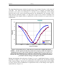
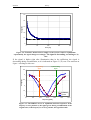
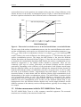
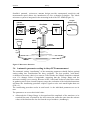
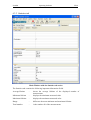
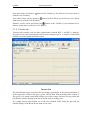
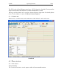
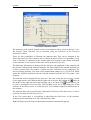
WT-1000B
USER’S MANUAL
Date of revision:
27.03.2008.
SEMILAB Inc.
Budapest, Hungary
Table of Contents
1
Introduction.......................................................................................................................1
Product Higlights ....................................................................................................................1
Specifications..........................................................................................................................1
2
Safety Information............................................................................................................3
3
Theory of the µ-PCD measurement ................................................................................4
3.1 Laser Excitation ..............................................................................................................4
3.2 Detection .........................................................................................................................4
3.3 Evaluation .......................................................................................................................7
3.4 Bulk and surface recombination .....................................................................................7
3.5 Lifetime measurement with the WT-1000B Wafer Tester .............................................9
3.6 Automatic parameter setting in the µ-PCD measurement ............................................10
4
Insatallation.......................................................................................................................9
Introduction.............................................................................................................................9
System configuration...........................................................................................................9
Facilities requirements .......................................................................................................9
2. Unpacking, inspection and preparing components of the system for installation ............10
WT-1000B main unit .........................................................................................................10
Other components of the system .......................................................................................10
3. Installation ........................................................................................................................10
Line voltage selection .......................................................................................................10
Installation of system components ....................................................................................10
System power and interconnections..................................................................................10
5
Hardware and software operation during the uPCD measurement ..........................13
6
µ-PCD Operating Software............................................................................................14
6.1 Introduction...................................................................................................................14
6.1.1
Requirements.....................................................................................................14
6.2 Installation ....................................................................................................................14
6.3 User Interface and basic operation................................................................................15
6.3.1
Main window .....................................................................................................15
6.3.2
Recorder tab......................................................................................................15
6.3.3
Statistics tab ......................................................................................................18
6.3.4
Lifetime tab........................................................................................................19
6.3.5
Details tab .........................................................................................................20
6.4 Menu structure ..............................................................................................................20
6.4.1
File menu...........................................................................................................20
6.4.2
Edit menu...........................................................................................................22
6.4.3
Measure menu Interface for ..............................................................................22
6.4.4
Options menu.....................................................................................................22
6.4.5
Macro menu.......................................................................................................24
6.4.6
Functions Menu.................................................................................................26
6.5 Toolbar..........................................................................................................................28
Semilab
Introduction
1
1 Introduction
Welcome as a WT-1000B Wafer Tester owner. The WT-1000B is a one-point non-contact
minority carrier lifetime measuring tool. It is capable of monitoring defects and
contamination both in the bulk and in the surface region of silicon blocks. It is a useful tool
for investigation and quality control of wafers, blocks and solar cells.
Product Higlights
•
•
•
•
•
•
Fully automatic operation and data evaluation
Measurement selectable at any position on the sample
Measurement of mono- and multi-crystalline material
Patented chemical surface passivation option available
Wafers can be measured after each process step of solar cell manufacturing
1:1 correlation with the standard Semilab WT-2000 Wafer Tester
Specifications
•
•
•
•
•
•
•
•
•
Materials:
Si, Ge
Resistivity range:
0.1 to 1000 Ωcm
Laser:
904 nm wavelength
Meas. spot diam.:
3 mm
Microwave source:
variable frequency around 10.3GHz
Lifetime range:
100 ns to 20 ms
Lifetime resolution:
0.1 %
Measurement time:
30 ms/data point
Single shot or continuous measurement
There are four Chapters to introduce the WT-1000 Wafer Tester system to you. There is a
description about the theory of the measurements and you can study how to install and
operate the system and how to use the software.
Safety Information
Instructions about the safe way of operating the WT-1000.
Theory of the measurements
It describes the theory of the lifetime measurement with the µ-PCD technique.
Installation
Semilab
Introduction
2
It gives information about the system configuration, specifications and the software
characteristics and explains how to unpack, install and start the operation of the WT-1000
system.
Operating software
It presents the user interface, and explains the capabilities of the software.
If you have any problem or question please do not hesitate to contact us.
SEMILAB
H-1117
Tel. :
Fax :
E-Mail :
Web site :
Semiconductor Physics Laboratory RT.
Budapest, Prielle Kornélia u. 2. Hungary
36-1-382-4530
36-1-382-4532
[email protected]
www.semilab.com
Semilab
Safety
3
2 Safety Information
The WT-1000B Wafer Tester contains high power pulsed infrared laser source; its
radiation is invisible by human eyes.
The WT-1000B Wafer Tester equipment is a Class 1M laser product, classified according
to EN 60825-1 standard because it is highly divergent. It is safe for the naked eye,
potentially hazardous when optical instruments are used.
The laser diodes of the PCD units are built in the measuring head. The invisible laser
radiation is emitted down perpendicular to the sample, placed below the measuring head.
During normal operation there is no risk of exposure to laser radiation.
Measuring head as well as laser diodes do not need any maintenance. In case of removing
any part of the protective cover from the industrial PC or dismounting the head unit,
scattered reflected invisible laser radiation might appear. Normally it is not harmful, but
should be avoided viewing directly to the fiber connection, the bottom of the measuring
head or using viewing optics to inspect any part of the equipment around the connector and
the stage under operation.
Semilab
4
Theory
3 Theory of the µ-PCD measurement
As the name implies, the technique involves the optical excitation and the signal detection
by the microwave system.
3.1 Laser Excitation
The pulse of an infrared
semiconductor laser generates free
electron-hole pairs under the
illuminated area on the sample
(Figure 3-1). Since the penetration
depth of the 904 nm wavelength
light is about 30 µm in silicon, the
free carriers are generated close to
the front surface of the sample.
measuring
head
hν
wafer
laser
pulse
σ0=f(n0)
σ0 + ∆σ
σ: conductivity
n: free carrier concentration
Figure 3-1: Laser excitation
measuring
head
3.2 Detection
µ wave
Since the free electrons and
antenna
holes
recombine,
their
concentration and so the
reflected
conductivity of the sample
µ wave
decreases after the excitation.
The decaying conductivity can
be monitored by detecting the
wafer
microwave reflectivity because
the reflected microwave power
is
proportional
to
the
conductivity of the sample
(Figure 3-2). It is measured as a
function of time.
Figure 3-2: Detection by micrwave
Semilab
5
Theory
The ring-shaped microwave antenna is used near to its resonance freqency, in the range of
10.0 GHz – 10.5 GHz. The sample and the antenna above it, compose a resonator, that’s
resonance curve can be seen on Figure 3-3, red line. As the conductivity of the sample
increases due to the excess carriers generated by the illumination, the resonance curve
shifts and gets deformed (Figure 3-3, blue line). As the excess carriers recombine, the
conductivity of the sample returns to equilibrium, and the resonance curve gets back to its
original state.
Pretuned
freqency
3.5
Voltage [V]
3
2.5
2
1.5
equilibrium
injected
1
10
10.1
10.2
10.3
10.4
10.5
10.6
Frequency [GHz]
Figure 3-3: Resonance curves of the microwave probe with a sample underneath.
(MWDC – the DC signal in the function of microwave freqency) When the sample is in
equilibrium, the curve is the red line. When the sample is injected, excess carriers are
generated by the illumination, the conductivity and reflectance is changed, the curve is
the blue line. The vertical green line shows the freqency used during the measurement,
pretuned so that the change of the signal is maximal.
During measurement, the microwave freqency is set to a predefined freqency (vertical,
green line on Figure 3-3). As the curve gets back to the original state, the measured signal
of the antenna changes. Because the recombination velocity is proportional to the number
of excess carriers, the recombination is exponential in time, so the change of the signal is
exponential too. (Figure 3-4)
Semilab
6
Theory
0.5
Voltage [V]
0.4
0.3
0.2
0.1
0
0
50
100
150
200
Tim e [us]
Figure 3-4: Transient, measured on a sample. As the carriers return to equilibrium
exponentially, the signal changes accordingly. The signal is descending, according to, b)
case.
If the signal is higher right after illumination than in the eqilibrium, the signal is
descending during recombination, as it is indicated on Figure 3-5, b) case. The transient on
Figure 3-4 belongs to this case.
a) growing
signal
3.5
b) descending
signal
Voltage [V]
3
2.5
2
1.5
equilibrium
injected
1
10
10.1
10.2
10.3
10.4
10.5
10.6
Frequency [GHz]
Figure 3-5: The MWDC curves in eqilibrium and after injection. If the
freqency is set to position a), the signal grows during recombination to the
original state, if the freqency is set to b) position, the signal descends.
Semilab
7
Theory
In some cases, the freqency is tuned to a position, where the signal of the injected sample
is below the signal of the sample in eqilibrium (Left part of the graphs on Figure 3-3). In
this case, the transient is reversed, the signal is growing by time during the recombination.
0.5
Voltage [V]
0.4
0.3
0.2
0.1
0
0
50
100
150
200
Time [us]
Figure 3-6: Transient with increasing signal, according to Figure 3-5, a) case.
3.3 Evaluation
The measured microwave reflectivity decay is fitted with an exponential curve and the
obtained time constant is recorded as the measured, effective lifetime in the given position
of the sample.
3.4 Bulk and surface recombination
The redistribution (homogenisation) of the free carriers takes place during and immediately
after the excitation. After this relatively fast event there are two main parallel processes
until the thermal equilibrium is reached (Figure 3.):
•
•
bulk recombination
carrier diffusion to the sample surface and then surface recombination
Semilab
8
Theory
τ diff
τ surface
diffusion of carriers
to the surface
Redistribution
Excitation
(generation
of
excess carriers)
surface
recombination
of
carriers
τ bulk
Thermal
equilibrium
bulk
recombination
Figure 3.: Block diagram of the sequence of processes during the µ-PCD
measurement
The measured lifetime characteristic of the whole recombination process as it is described
with the following equations:
τ
1
=
meas
τ
1
bulk
+
τ
diff
1
+
τ
τ diff =
d2
π 2 ⋅ D n,p
τ surf =
d
2 ⋅S
surf
where:
•
τbulk is the bulk recombination lifetime that is characteristic of material quality.
•
τdiff is the characteristic time necessary for carrier diffusion to one of the
surfaces of the wafer from the place of excitation. It is determined by the wafer
thickness and the diffusion constant of minority carriers.
•
τsurf is the characteristic time of surface recombination, determined by surface
recombination velocity.
It is short for polished bare
-1
(S ≈ 50000 cms ) and long for passivated wafers (S < 10 cms-1).
wafers
•
τmeas is the measured lifetime.
•
d is wafer thickness.
•
Dn and Dp are diffusion constants of the minority carriers, for electrons and
holes.
•
S is the surface recombination velocity.
Semilab
9
Theory
As described above in the equations, the sample surface may have a large influence on the
lifetime because of the surface recombination process. Figure 4. shows theoretical data of
the basic equation calculated for three different surface recombination velocities.
10000
S=1 cm/s
With chemical passivation
S=10 cm/s
1000
100
Diffusion lifetime
S=50000 cm/s
Without chemical passivation
10
1
1
10
100
1000
10000
Bulk lifetime [µs]
Figure 4.: Theoretical correlation curves of the measured lifetime versus bulk lifetime
The two steps of the surface recombination process, the free carrier diffusion to the surface
and the recombination at the surface are described with two independent parameters (τdiff
and τsurf). If the surface recombination velocity is very high, τsurf is very small (typically
on bare surfaces), the carrier diffusion is the limiting process i.e. τdiff describes the whole
surface recombination process. The longer the bulk lifetime is the more the diffusion
lifetime determines the measured lifetime (Figure 6.). Since the aim of the measurement is
to determine the contamination dependent bulk lifetime, the surface recombination process
should be suppressed i.e. the sample surface should be passivated. There are two
commonly used ways of surface passivation, the thermal oxidation and the chemical
passivation. Depending on the efficiency of the passivation, bulk lifetimes much longer
than the diffusion lifetime can be measured. Although the measured lifetime depends on
both the bulk and the surface recombination processes, in special cases it refers to either
the bulk or the diffusion lifetime. Approximately the bulk lifetime is measured if the
measured lifetime is much shorter than the diffusion lifetime (high contamination level)
independently of the surface recombination velocity. The bulk lifetime is measured in the
case of passivated surface as well. The diffusion lifetime is measured if the surface
recombination velocity is high (bare sample) and the bulk lifetime is much longer than the
diffusion one (low contamination level). In this case the obtained lifetime map is very
homogeneous since the diffusion lifetime depends only on the sample thickness and the
diffusion constant of the minority carriers which parameters typically do not change a lot
in a sample.
3.5 Lifetime measurement with the WT-1000B Wafer Tester
The WT-1000B Wafer Tester is a fully computer controlled equipment. The measured
transients are recorded by the transient recorder card.
Semilab
10
Theory
Semilab’s patented microwave antenna design provides unsurpassed sensitivity and
measurement speed allows the introduction of new evaluation principles. The whole
microwave system is integrated in the measuring head of the WT-1000B (Figure 5.).
scope
(trans. rec.)
µ wave
generator
circulator
detector
isolator
flat finder
laser
diode
µ wave
antenna
IR
light
wafer
Figure 5. Microwave detection
3.6 Automatic parameter setting in the µ-PCD measurement
The automatic setting “AutoSetting” of the measuring parameters should find an optimal
setting taking into consideration the above problems. The best possible "wide-band"
evaluation is necessary, that is in a concrete Time Window the lifetime should be evaluated
even if it changes orders of magnitude, supposing that the Voltage Range and the
microwave tuning is set correctly. Because of this "wide-band" behavior which also results
in gathering noise from a broad frequency range the evaluation of the individual transients
and hence the AutoSetting procedure requires signal to noise ratio much higher than one
(S/N>>1).
The AutoSetting procedure works in serial mode i.e. the individual parameters are set in
turn.
The parameters are set to their initial value:
•
Afterwards the Voltage Range is decreased until the amplitude of the transient (or its
recorded first part) is optimal for the A/D conversion, and at the same time the extreme
values of the transient are also far from the scope boarders. (AutoRange)
Semilab
•
•
•
•
Theory
11
Due to the laser pulse there is a step at the beginning of the transient that should be
maximized by changing the microwave frequency in large steps with the necessary
increase of the Voltage Range. (PreTuning)
With this not optimal but adequate tuning an approximately optimal Time Window can
be found which results in valid lifetime data within the Time Window. Especially in
case of strongly distorted transients, it can occur that the resulting Time Window is
longer than the optimal one. After the Time Window setting the number of averaging is
corrected to an approximate optimum value. (AutoTimeWindow)
After setting the Time Window the fine tuning is performed by searching for the
maximum of the correlation function that characterizes the "energy" of the transient
weighted by an exponential decay of optimal lifetime value. This way the tuning is
independent of both the distortion and the fact that the evaluation is reasonable or not.
In general this process gives better microwave frequency than the PreTuning
procedure. (Tuning)
After the tuning procedure the Time Window is corrected if necessary and if the Time
Window correction consists of more than one step then the tuning process is repeated
followed by a new Time Window control.
Semilab
Installation
9
4 Insatallation
Introduction
The WT-1000B Wafer Tester system is a computer controlled equipment which is suitable
for recording, storing and displaying minority carrier lifetime of silicon wafers.
System configuration
Basic units:
•
•
•
Measuring head
Industrial PC (Windows operation system)
Pheripherals (keyboard, mouse, LCD monitor)
Facilities requirements
Indoor environment
Operating temperature:
between 15°C and 35°C
Relative air humidity:
10% to 80%
Maximum height above sea level during operating: 2000 m
For detailed specifications of other components of the total system please refer to their
own manuals supplied with them. Specifications in next paragraphs concern the main unit
only.
Power line supply
Line type:
single phase, phase-neutral-protective ground system.
Line frequency:
50-60 Hz.
Input voltage:
115 Vac or 230Vac +10 % with manual selection.
Power consumption:
maximum 300 VA.
Power line connection:
1363 plug.
1.8 m long, 3-wire 3 x 0.75 mm2 power cable with BS
Class of hazardous electrical shocking:
green/yellow color.
Overvoltage group:
class
I,
II, according to IEC 664.
protective
conductor
with
Semilab
Installation
10
2. Unpacking, inspection and preparing components of the system
for installation
WT-1000B main unit
Unpack and remove the Wafer Tester WT-1000B the industrial computer and other units
like, the monitor, the keyboard, the mouse etc. from the crates.
Check the crate contents according to the packing list.
Inspect the system if there is any damage observable. Report damage to shipper
immediately.
Be sure that the exterior of the instrument was not damaged. Any deformation on the
exterior of the instrument can influence the operation of it.
If any part of the instrument got loose during shipment, it can cause an inaccuracy in the
result of measurement, therefore tighten them before use.
Other components of the system
Unpack all of other components of the system and please refer to their own manuals
supplied with them for instructions.
3. Installation
Caution!
Be sure that the available power line voltage/frequency corresponds to the
setting on industrial computer (115 Vac or 230 Vac).
Line voltage selection
Line voltage should be set manualy on the industrial computer only. There is a red voltage
selector on the backpanel of the industrial computer. Please check swich position before
connecting system to the mains.
Installation of system components
For further information on system components (computers, monitor, mouse, keyboard and
printer) please follow the instructions found in their own manuals supplied with them.
System power and interconnections
Caution!
All electrical conections of the system should be performed with switched
off power and unpluged line cable!
The following list gives short description of the cables and their interconnection. For
socket numbering please refer to Image2 after the cable descriptions.
Semilab
Installation
11
µ-PCD cable. This cable makes connection between WT-1000B lifetime measuring system
and the transient recorder in the measuring PC. One end of this cable should be plugged
into socket no. 1.on the industrial computer and the other into socket on the WT-1000B
main unit (see image and table of interconnections later).
µ-PCD cable
UTP cable for LAN connection. An UTP cable for Local Area network connection is also
delivered with the system. It should be plugged to connector no. 4. of the industrial PC and
the other end to the LAN wall connector or HUB.
UTP cable for LAN connection
Mains cable. One mains-cable is delivered for the industrial computer (plug to connector
no.2 on the industral PC back panel). Besides this all other componets (monitor, printer
etc.) have their own mains cables in their own package.
Mains cable
Semilab
Installation
12
Measurement head
WT-1000B measurement configuration
Industrial PC back panel
For software installation and operation please refer to Chapter 6. µ-PCD Operating
Software
Semilab
Installation
13
5 Hardware and software operation
during the uPCD measurement
WT-1000B is optimized for Si blocks and not for wafers. The problem with the wafers is
that the sensor is sensitive to the holder which is below the wafer. This problem is solved
for the WT-1000 because this system has a measurement stage.
This head has the same structure as the WT-1000. The operational software is the same
also.
Bottom of the sensor of the sensor has to fit to the sample. So, during the measurement the
whole measurement head is sitting on the surface of the sample.
The black plastic part of the sensor touches the sample.
Before the uPCD measurements do not forget to use the AutoSetting procedure, which is
described in Chapter 3.
Semilab
Operating Software
III/14
6 µ-PCD Operating Software
6.1 Introduction
6.1.1 Requirements
For proper operation the following requirements should be fulfilled:
Software requirements:
•
MS Windows 98, NT, 2000 or XP.
Hardware requirements:
•
•
Pentium compatible computer running the Microsoft Windows operating system
Optional windows compatible printer
6.2 Installation
The software is installed on the computer shipped with the WT-1000B System. The
software is installed into ‘C:\uPCD\’ directory. The WinRt program should also be
installed for correct operation. The measuring program can be started by the following
shortcut:
Semilab
Operating Software
III/15
6.3 User Interface and basic operation
6.3.1 Main window
Running the uPCD software the following window appears.
Main window/Recorders tab
The window has four main parts: Menu Bar – at the top of the window just below the
window title, Toolbar – below the Menu Bar, Statusbar – at the bottom of the main
window and the working area between the Toolbar and the Statusbar.
The working area of the uPCD software consists of four or five tabs: Details, Statistics,
Lifetime and Recorder
6.3.2 Recorder tab
There are the measuring parameters and the plot window, which displays the transient in
the Transient Recorder window.
The Microwave Frequency, the Averaging, the signal Range (Y-axis of the Scope window)
and the Time window (X-axis of the Scope window) are automatically set by the
Autosetting procedure. Autosetting can be reached from Measure/Autosetting menu item,
or clicking on the
icon on the Toolbar.
Semilab
Operating Software
III/16
LT (transient evaluation method)
It defines the method for transient evaluation. There are three different methods, the socalled Semilab method, which was developed by Semilab, the 1/e and the 1/e2 methods.
The Semilab method can be used with different number of points taken from the transient
from the Time Cursor. The Time Cursor is the vertical line in the Scope window, which
determines the point from where the recorded data are evaluated to avoid the initial,
distorted part of the transient. The evaluated points are displayed with blue color and their
number may be 64, 128, 256, 512 or 1024 (The whole, recorded transient consists of 2048
data point). In most cases it is recommended to use 1024 points. The fitted lifetime is
displayed near the LT drop-down box in µs units.
Time curs.
The above-described Time Cursor is set automatic (Auto) by default i.e. the software
automatically determines its position after recording a transient according to a built-in
algorithm. If it is set manual (checkbox is unchecked), you can determine its position by
dragging the cursor line by the mouse in the plot window. It is recommended to use it in
automatic mode to get reliable and reproducible results. By the proper setting of the cursor
the non-exponential initial part of the decay (e.g. due to redistribution of carriers) is
avoided and only the carrier recombination transient is analyzed. The position of the Time
Cursor is displayed near the Time curs. checkbox in µs units.
Averaging
Averaging is the number of transients taken and averaged at a given position. The possible
values are 1, 4, 16, 64 and 256. More averaging means an increased signal to noise ratio at
the expense of longer time necessary for the measurement.
Amplitude
The signal amplitude in the transient at the Time Cursor position is displayed also in the
Settings panel in mV units. It may happen when parameters are set manually that the
beginning of the transient is out of the Voltage range thus the displayed Amplitude value is
not of the whole transient. One possibility is to drag the horizontal dashed line (Offset)
and set to a position where the whole transient is inside the range. If the transient
amplitude is higher than one third of the Voltage range it is recommended to set to higher
range.
Thickness Correction
If the bulk lifetime is comparable to the characteristic lifetime, coming from the surface
recombination and diffusion, the bulk lifetime can be calculated, if wafer thickness and
surface recombination velocity is known.
Click the button right from the “Thickness Correction”, and type in the window the wafer
thickness, the surface recombination velocity, and click the p or n type of the wafer. If the
checkbox on the left is selected, the software calculates the bulk lifetime according to
chapter 1.4. This calculated value is displayed in place of the measured lifetime.
Microwave frequency (tuning)
The reflected microwave power depends on the microwave frequency. As a consequence
the measured transient amplitude also varies with it. The tuning is: finding the microwave
Semilab
Operating Software
III/17
frequency where the signal has its maximum amplitude. The microwave frequency can be
modified within a 500 MHz range by dragging the slider or using the small arrows near the
slider. The basic frequency is 10 GHz.
Laser Power
The excitation level (number of excess carriers generated) is proportional to the laser
power. By the application of different laser powers, transients at high and low excitation
levels can be measured and compared leading to valuable information on the
contamination species or oxide quality. In the default case high power is suggested
(120E11), this way a good signal to noise ratio is achieved.
Range (Laser Power)
The Laser Power can be changed easily with an order of magnitude (low and high range).
Range/Voltage (plot window)
The Y-axis of the Scope window is the signal amplitude: the output voltage of the
microwave detector. Depending on the signal level, different sensitivities can be selected
such as 1, 2, 5, 10, 20, 50, 100, 200, 500 mV and 1 and 2 V. In case of highly conductive
material (0.1-1 Ωcm) the relative change in conductivity due to a given laser pulse is
small. As a consequence high sensitivity should be selected. On the other hand
measurements on wafers with high resistivity are normally performed with low sensitivity
(large amplitude range) due to high amplitude. The proper selection of the sensitivity range
is when the signal amplitude is between the 50% and 70% of the whole range. Use of
Autosetting procedure is recommended.
Range/Time (plot window)
The X axis is the time elapsed after starting of the transient recording (the zero point is
before excitation). The time ranges available are 0.05, 0.1, 0.2, 0.4, 1, 2, 4, 10 and 20 ms.
In case of a proper setting the fitted decay time should be about 1/5 - 1/10 part of the
whole range.
Semilab
Operating Software
III/18
6.3.3 Statistics tab
Main Window with the Statistics tab active
The Statistics tab contains the following important information fields.
Average lifetime
-
shows the average lifetime of the displayed number of
measurement
Minimum lifetime
-
displays the minimum measured value
Maximum lifetime
-
displays the maximum measured value
Range
-
difference between minimum and maximum lifetime
Total number
-
is the number all of the measurements
Semilab
New data can be recorded by
with the Ctrl+N hotkey.
Operating Software
III/19
button in the Toolbar, by the Measure/New menu item or
New batch of data can be started by
menu item or with the Ctrl+B hotkey.
button in the Toolbar, by the Measure/New Batch
Statistics can be saved and cleared by
button in the Toolbar, by the Measure/Clear
Statistic menu item or with the Ctrl+L hotkey.
6.3.4 Lifetime tab
Lifetime tab is mainly used for inline applications (Semilab WLL 1 and WLL 5 models).
Its purpose is to stop measurement and even the transport belt if a sample is found with
lifetime out of the specified lifetime region.
Lifetime Tab
The ideal lifetime range is between the two orange colored line. If the measured lifetime is
in this region the colour of the plot is green. The lifetime field in the Recorder window is
also green. If a sample found with lifetime out of the orange coloured Warning limits the
plot and the lifetime display in the Recorder tab turns to orange color.
If a sample found with lifetime out of the red coloured STOP limits the plot and the
lifetime display in the Recorder tab turns to red color.
Semilab
Operating Software
III/20
The WLL series in-line lifetime testers have a 24V I/O interface. Both the Warning and the
Stop levels are sent to this interface to control external device events.
Warning and Stop limits can be set from Options/Lifetime Setup menu. For details please
refer to ist description in chapter 3.4 Menu structure/Options.
6.3.5 Details tab
Details tab is a sensible and useful combination of the Statistics and Lifetime tabs.
Details tab
6.4 Menu structure
6.4.1 File menu
View Transient
The Transient Evaluation window appears with the last measured transient.
Semilab
Operating Software
III/21
Transient Evaluation window
The transient can be loaded, printed or the current transient can be saved to disk (to ‘*.trn’
file format). These functions can be activated using the self-menu of the Transient
Evaluation window.
There are four possibilities to illustrate the transient data. They can be changed in the
Mode drop-down list. The transient can be plotted on linear (Linear) or logarithmic (Log)
scale. It can also be illustrated as the output signal of a frequency scan (Scan) performed
on the transient or as a function of the time cursor position (Cursor-LT).
The following information is displayed in the Info area: the amplitude of the transient and
the lifetime evaluated with different methods. The first method is the Semilab method (text
is black colored). Here the number of points used for evaluation can be changed by the
arrows pointing up/down. The name of the method than changes to e.g LT(Sl/512) which
means the lifetime calculated with the Semilab method from the first 512 points of the
transient.
The transient itself is displayed in the plot area. The axes of the plot area can be re-scaled
by the small arrows at the bottom and the right side of the plot. By pushing the
button at
the middle of the right side the original scaling can be set again. The
button allows you
to select a rectangular area in the plot. This handling is true for all appearing plots in the
software. If the mouse cursor is on the plot area, its coordinates appear in the Statusbar of
this window.
The transient data can be copied to the clipboard by Edit/Copy Data menu item, or can be
copied as an image by Edit/Copy Picture.
In the View menu there is a possibility to show/hide the fitted curve of the transient,
change transient and fitted curve line color and line width.
Right clicking below the Info area detailed measurement information appears:
Semilab
Operating Software
III/22
Save Transient
Saves the actual transient to a `*.trn` file. This file can be loaded later in the File/Load
menu of the Transient evaluation window.
Exit
Closes uPCD lifetime measurement software.
6.4.2 Edit menu
Copy Data
-
Copies current transient data to the clipboard
Copy Picture
-
Copies current transient as an image to the clipboard
6.4.3 Measure menu Interface for
New
-
performs a measurement and adds data to statistics (see
Statistics tab description in Chapter 2.1)
Clear Statistic
-
clears statistics
Select
-
a submenu appears where the active head can be selected for
the Recorder window (for Semilab WLL-5 five point system)
Autosetting at..
-
The point selected in Measure/Select menu is used for
automatic parameter setting. In this case all the five heads
will use the same settings.
Autosetting All
-
The Autosetting procedure is performed at all the measuring
points. In this case all the heads use different settings.
Stop Autoset.
-
Stops Autosetting procedure. Shortcut key: Ctrl+P
6.4.4 Options menu
µ-PCD Interface
24V I/O Interface
here you can choose between 2 ports, there is a possibility to
use 2 measuring heads
-
If the measuring system is equipped with 24V interface card
(WLL series only) it is possible to send start/stop signals to
the main unit and control transport line according to
measurement results. If interface card is not installed select
Not Used.
Semilab
Operating Software
III/23
Serial TRG/WID
-
Triggering is also possible via a serial port, or this port can
be used for sending wafer-ID-s, if you click the Settings
button , you can reach the Communication Setup panel.
Fast Transient
-
Only 1024 points are recorded by the Transient Recorder
instead of the standard 2048.
Polarity Selector
-
The microwave reflection changes with frequency (see 3.6
Functions menu). If the frequency is tuned before the peak
the transient has negative polarity. If the frequency is tuned
after the peak the transient changes to positive polarity.
Polarity selector gives the possibility to force Autosetting to
tune the frequency before or after the peak.
Exclude 50 µs Time Range The shortest time range is not used by the autosetting
procedure.
Optical. Sensor
-
A submenu appears: After placing a sample under the head
the optical sensor detects that. If Used is checked a
measurement is performed automatically after detecting the
wafer. The delay in millisecond units between sample
detection and measurement can be set in Sense Delay input
field.
Local Mode
-
Voltage on the optical sensor output is measured. This
voltage depends on the reflectivity of the material under the
sensor. There is a comparison level limit to decide if the
empty stage or a sample is under the sensor. Above the set
limit it senses stage, below that it senses wafer. The default
value is 4.5V.
Semilab
Operating Software
III/24
Lifetime Setup
-
The upper and lower Warning and STOP levels can be set in
the appearing input window (for levels description please
refer to 2.4 Trend menu).
TLV Setup
-
Total Lifetime Variation Setup
Upd.With Stat.
-
In case this option is activated when update checkbox is
selected
(see Chapter 4.), the continously
measured data is added to the statistics.
Slope Correction
-
The microwave DC level sometimes changes even during the
measurement and it results in a distorted transient shape. The
Slope Correction procedure takes the slope of the microwave
DC level into account when evaluating the transient.
You can in this menu Load and Save the measurement settings and the Classifications (for
Classifications description please refer to 2.3)
6.4.5 Macro menu
The Macro language has been implemented in uPCD to give users a wider range of control
over software capabilities. It is a special program language that is mostly similar to BASIC
or DOS batch programming.
Semilab
6.4.5.1
Operating Software
III/25
Macro
Clicking Macro/Macro menu item the Macro Editor window appears:
To handle the macros you have the following tools:
Create new macro
Deletes the selected macro
Runs the selected macro
Checks for Syntax Errors in the selected macro
Lists all available macro variables, functions and procedures
Prints the selected macro
Cuts the selected text from the selected macro
Copies the selected text from the selected macro to the Clipboard
Pastes text from the Clipboard to the selected macro
You can also give menu access to the macros by typing a name in the left-bottom edit-box
and then the new menu item appears below the Macro menu item in the Macro menu.
Macro Syntax
For more detailed information on macro possibilities refer to the Macro Syntax window by
pressing the
button in the Macro Edit window or Macro/Macro Syntax menu item.
Macro Watch
There is a debugger for macro language built in uPCD. You can add watches by
Macro/Watch menu item. On the appearing Watch Window use right mouse button to
choose from the possibilities:
Semilab
Operating Software
III/26
Clicking on Macro Syntax a list of all available variables, functions and procedures
appears.
Here you can check the sintax and finde sintax errors and set the editor fonts properies
6.4.6 Functions Menu
Functions menu contains the measuring possibility of the following functions:
Microwave DC
Plots the microwave reflection (mV units) versus the applied frequency. Checking the Free
Running checkbox at the top-right the plot is repeatedly recorded.
The MWDC curve should be a non-monotonic (typically it has a minimum) curve between
the 0V and the 5V limits measured on samples from a wide resistivity range (from
insulator to metal).
Microwave DC
Laser Control Monitor
The Control Voltage versus Laser Power curve is measured in this window. It serves for
checking the stabilization of the laser. The curves should increase monotonically and
should remain below the Control Limit.
Semilab
Operating Software
III/27
Laser Control Monitor
Lifetime – Time
The lifetime as a function of the time curve is recorded in this window. The measuring
interval can be set between 0-250 [sec] by dragging the dT slider. When dT is set to 0, the
maximum available measuring speed is selected. The Sampling determines how many
measured values are averaged before recording a point on the plot.
Lifetime – Time
Lifetime – Laser Power
The lifetime versus Laser Power curve is measured in this window. The resulting curve
(logarithm of lifetime versus Laser Power) is typically increasing and it can be fitted with
straight line. The slope of the line may be characteristic of the dominant contaminant in the
wafer.
Semilab
Operating Software
Lifetime – Laser Power
6.5 Toolbar
The toolbar gives fast access to te following functions:
-
Activates Autosetting procedure
-
Stops Autosetting procedure
-
Performs a measurement and adds data to the statistics
-
Clears data from statistics
-
If checkbox is checked, the transient is updated continuously
III/28