1
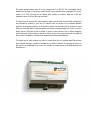
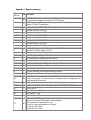
User Manual for ModbusRTU compatible
I/O-interface board IT8888-4 and IT5888-4X
1. Introduction
This input/output (I/O) -board is a universal interfacing device used to link computer networks with
the real world environment, both in home/office or light industrial environment. To the network side
the board has one RS485 interface and one 3.3V serial interface (IT5888-4) or one Ethernet
interface (IT5888-4X with Lantronix Xport installed).
The usable communication protocol is ModbusRTU, at speeds from 9600 to 115200 bps. Towards
the real world environment there is a number of protected binary or analogue channels available,
like up to 16 binary inputs, 8 binary outputs and 8 analogue inputs in various configurations. Dallas
1-wire bus interface is available as well, supporting up to 9 temperature sensors DS18B20 and up
to 9 DS2438 devices (multichannel ADC).
The power options include either 5V or any voltage from 7 to 35V DC. The consumption mainly
depends on the load on the binary outputs (these can be supplied from a separate DC source,
usually 12 or 24V). The outputs can directly drive resistive or inductive loads up to 3W with
maximum current of 200 mA per output channel.
The device has an on-board PIC-microcontroller, taking care all of the communication, multiplexing
and calculations needed to sync the I/O channels with the content of the available Modbus
registers. Some useful properties of the board to mention are the built-in 32-bit counters for each
binary input and the ability to generate pulses with exactly controlled length from 1ms to 4s on the
binary outputs. The board is able to supply 5V power to other devices, with or without watchdog
reset functionality. The watchdog is able to cut the 5V power to the external device for a predefined
time in case of no Modbus communication detected for another predefined time.
The board can be easily (without any tools or screws) fitted into a 6 modules wide DIN-rail case
from Camden, making it suitable for installations into electric cabinets. In the same case there is
also room for an embedded Linux control unit, should it be needed (check for DC6888 product from
Droid4control).
2. Technical specifications
•
Supply voltage 8..35V DC, current 30 mA max @12V (without load on output)
•
8 channels of sourcing outputs (DO),
10..27V, load current up to 200 mA
- configurable power-on level;
- single or periodical pulses from 1 to 4095 ms ;
- pulse period up to 65 s in 1 ms steps.
•
8 channels of binary inputs (DI), active high or low
- 4 inputs usable for up to two Wiegand readers;
- 32 bit counter on every input;
- maximum input voltage 27V.
•
8 universal channels (AI/DI/DO), bitwise settable to
- 12-bit analogue input 0..2V/0..4V/0..5V/0..10V
or 0..20mA;
- binary input low or high active;
- high impedance binary output 0 or 5V / 10k;
- maximum input voltage 27V..
•
RS485 interface, from 9600 to 115200 bps,
ModbusRTU protocol supported in firmware
•
1-wire interface for up to nine DS18B20 and nine DS2438 devices
•
5V 500 mA protected supply voltage for external devices
•
On-board LED-indicators for RS485 TX, RX, 5V power interface, 5V reset
•
Board dimensions 86x103mm,
fitting into a 6 DIN-rail modules wide plastic case from Camden (106mm width)
3. Power options
The board can be supplied either from a stabilized 5V voltage source or from any DC source with
output voltage from 7 to 35V. In the first case the power is supplied to the connector XW pin VS or
to the pin1 of connector JU2 in the middle of the I/O-board.(see the print on the PCB or follow the
labels on the case if a cased product was purchased).
The typical usage scenario in the first case is that the controlling device (Modbus Master) will feed
the 5V supply voltage to the board. For example, there are USB-serial converters available both for
3V3 serial or RS485, that can output 5V in addition the communication signals. power It is also
possible to use a USB/serial converter cable connected to JU2 for 5V supply feed via pin1. A
suitable product for this kind of approach is USB-RS485-WE-1800-BT from
http://www.ftdichip.com, if 4 of the bare wire ends (5V, RX, TX, GND) are soldered to a 2.54 mm
header connector matching JU2.
Another way is to generate 5V from a voltage up to 35V supplied to XS.VS. The on-board regulator
is able to provide 1.5A 5V power that can be used to supply some external devices or a local
control unit.
It must be noted that powering the I/O-board with 5V via connectors XW or JU2 does not supply the
driver for the binary outputs. If the binary outputs are in use, then the voltage matching the
requirements of the loads must be supplied to the pin VO or connector XS (the ground pin on that
connector is common for VS and VO). All of the output channels will use the same supply voltage
on pin VO. The actual voltage on the load will be 2V lower than the supply voltage on pin VO of the
connector XS.
The supply source for the pins VS and VO of the connecter XS can also the same (in which case
both of these pins are connected together). But in many cases separate powering is preferrable.
For example, pin VS could be supplied with battery-backupped voltage from 11 to 14V and pin VO
with 24..27V supply without battery backup (assuming there are 24V loads connected to the binary
outputs). Should the mains power outage occur, the binary outputs become idle but the ability to
communicate and monitor the inputs is not lost for the I/O-board. Also the devices consuming 5V
from the board are still operational.
If the device consuming 5V from the board is connected to JU2 on the board, then iti is possible to
take advantage of the watchdog timer functionality built into the board firmware. By setting the
register with address 276 to a delay in seconds instead of default value 0, the power on pin1 of JU2
is cut off after that time without Modbus-communication. The length of the power cut pulse (in
seconds) is defined by the content of register with address 277 (see also the Appendix 1).
4. Digital communication
There are in total five digital communication channels available to the outside world on the I/Oboard. Two of them (RS485 and 3.3V serial) are transparent to each other and also to the PIC
microcontroller, being used to read and write the I/O registers on the board using ModbusRTU
protocol (see the Appendix 1 for detailed register information). One additional interface is for 1-wire
communication with DS18B20 or DS 2438 devices. Two listen-only interfaces are available for the
Wiegand-readers, using these will reduce the number of available DI channels by 2 per Wiegandreader.
4.1. Modbus-communication
is available using ModbusRTU protocol, either on RS485 bus via connector XM or as 3.3V
level serial communication via pin header JU2. Thus together with the on-board PICmicrocontroller there are three communication parties that share the content of the
communication at speeds from 9600 to 115200 bps.
At all times only one of these three parties can send, other two are listening. Without active
communication, all parties are in listening mode. The direction control of the RS485 port is
taken care by the on-board PIC-microcontroller, even if the communication is taking place
between the devices behind 3.3V serial and RS485 interfaces without involving the registers
on I/O-board. All of the serial devices connected to the I/O board via either RS485 or 3.3V
serial port should share the same communication parameters as the on-board PIC.
The data may arrive to JU2 from any suitable control device, either directly from 3.3V UART
or via USB/serial converter cable, using low level active signal state. There is 5V power pin in
JU2, so the controlling device can either supply the I/O-board or be supplied from I/.O board
(see 3. Power Options above).
The default parameters for Modbus communication with the on-board PIC-microcontroller are
19200 bps, 1 start bit, 1 stop bit, even parity. The speed and parity may be changed via
setup registers on addresses 274 and 273 (see the Appendix 2). It is important to keep in
mind, that once the communication parameters are changed compared to their default
values, the communication using ModbusRTU-protocol must be regular. If there is a pause in
the communication for more than 30 seconds or if the content of the messages cannot be
understood by the PIC-microcontroller, the communication parameters of the PIC
microcontroller fall back to the default parameters (19k2 8E1).
If the controlling device is powered by 5V (500 mA max) supply from the board via pin1 in
JU2, then it is possible to set up a watchdog timer to reset the controlling device if no
Modbus-communication is detected by the on-board PIC for the time in seconds stored in the
register with address 276 (see also 3. Power Options above).
If the I/O-board has Lantronix Xport installed, then instead of 3V3 serial connector JU2 the
Ethernet connection can be used. The communication protocol is still ModbusRTU, not
ModbusTCP. The communication parameters of the Xport are set to the default values of the
on-board IC, being 19k2 8E1.
To use 3V3 serial connector JU2 from the board with Xport installed, the jumpers SJ1 and
SJ2 on the PCB must be disconnected by using the soldering iron. This disconnects the RX
and TX signals from Xport to avoid conflicting 3.3V serial signals.
4.2. 1-wire communication
The I/O board supports up to 9 DS18B20 and up to nine DS2438 devices simultaneously, on
a shared bus available on pins 1W (signal) and GND (ground) in the connector XW. On the
same connector 5V supply (protected with resettable 500mA fuse) is available for the 1-wire
(or other external) devices.
The temperature sensors DS18B20 can be used without the power line, in parasitic power
mode with power pin grounded. The I/O-board will provide power pulses before read
command, ensuring reliable communication with DS18B20 devices on room temperatures
and below. On higher temperatures using the dedicated power instead of parasitic power is
suggested. There is no need to make any adjustments in the setup registers for that, just
using 5V power on the sensors measuring higher temperatures is enough. It is also possible
to mix DS18B20 sensors in parasitic mode and powered with 5V on the same 1-wire bus.
The DS2438 devices must always be supplied, there is no parasitic power option for them.
Other than 5V supply voltages are possible for them.
See the Appendix 1 for reading the data from 1-wire sensors.
4.2. Wiegand-communication
Up to two Wiegand-devices with message length up to 40 bits are supported. Each Wieganddevice needs two data lines to be connected,. Two or four binary input channels (DI5..DI8)
can be switched to Wiegand mode via register with address 273 (See the Appendix 1).
The pull-up switches for the DI-channels used for Wiegand communication must be manually
switched to ON in order for Wiegand inputs to function. The length of the received messages
together with the received data is available on registers with addresses from 10 to 18.
5. Using binary inputs
The maximum number of binary inputs is 16, eight of them being are available in DI port via the
connector DI and the rest in the universal ANA-port (via the connector XA). The input data is bitmapped to the holding register with address 1, where the eight most significant bits correspond to
channels DI1..DI8 and the least significant bits correspond to the channels marked as AI1 to AI8.
The binary inputs are equipped with digital filter, cleaning the input signal from contact bounces
shorter than 4ms. There is no change detection used in binary inputs. To catch the short pulses
that may be present between the reads of register with address 1, either the counter state can be
checked or the so-called “sticky bit”- mode can be used. In the latter case no more than one
change is allowed to each bit in the holding register with address 1 between two readouts.
The active level of the input signal (high or low, default is high) can be changed by setting the mask
in the input inversion register with address 271 (see the Appendix 1).
6. Using counters
The 32 bit counters are available for every input channel in binary input mode. They can be read or
written as two consecutive holding registers per counter (see the Appendix 1). The active edge
(falling or raising) can be selected with the input inversion mask register with address 271.
Do not switch off “debounce” filter and do not use “sticky bit” option if you are using counters.
These options set by the certain bits in register with address 273 (see Appendx 2) have currently
effect on all binary input channels of the I/O board (this will be changed to bitwise setting per
channel in a future firmware release).
7. Using binary outputs
The eight binary outputs are capable of feeding 200mA DC current to both active and inductive
loads. The voltage on the load depends on the supply voltage VO supplied to the I/O-board via the
connector XS. The voltage VO should be selected somewhat higher than the nominal load voltage
due to 2V voltage drop on the output driver circuit.
The output channels are protected against overload by the resettable fuse on every output. The
outputs are also protected against the voltage spikes above 27V. Thus the damper diodes on
inductive loads (like relay coils) can be skipped, if the load is close to the I/O board. With longer
lines to the load the damper diode should still be connected as close as possible to the inductive
load to prevent emitting electromagnetic disturbances.
8. Using analogue inputs
The analogue input channels (up to 8) are available on ANA port. The channels must be configured
correctly in order to use them. First, the mask (with default value 0) defines in register with address
275.
The I/O-board incorporates a PIC microcontroller with 12-bit ADC. The analogue measurements
are constantly averaged in the board firmware in a window of 10 values to improve the readings
stability (skipping the minimum and maximum readings before averaging).
For trustworthy measurements the correct reference voltage defining the maximum measurable
value on the ADC input must be set by writing the register with address 270. There are three
possible values for that register to select the reference voltage: default 0 activates external
reference voltage from power supply (5.0V); value 48 activates 4.096V internal reference voltage
and value 32 activates internal 2.048V reference. It is usually best to use 4V reference voltage, as
this provides depending on the jumper positions either direct mV readings or 10V or 20mA full
scale.
9. Generating analogue output
The board does not incorporate dedicated analogue outputs, but using the universal I/O-channels
provided by ANA port the controlled analogue voltage with up to 8 bit precision can still be
generated. For this the number (equal to the desired bit count) of sequential channels from ANA
port count must be configured as binary outputs. Between the output pins the resistors with value
of 15 kiloOhms and with precision of 0.1% should be connected (see the connection diagram
below). By writing values to the according bits in the register with address 0, the voltage on the
analogue output is controlled in the range from 0 to 5V.
10. Working with 1-wire devices
The digital Dallas 1-wire interface is provided on the connector XW. Up to nine DS18B20
temperature sensors plus up to nine DS2438 battery monitor devices (multi-channel differential
ADC devices, both data and ID) can be read from the registers on the board.
The temperature readings from the DS18B20 sensors are 12 bit signed values in 9 registers
starting from register address 600. The values read must be multiplied to 5 and divided by 80 to get
Celsius degrees. While the I/O board provided parasitic (pulse before reading) power to the 1-wire
data line ensures reliable usage of the DS18B20 sensors at room temperatures and below, a
dedicated 5V power to the temperature sensors is needed to use them at higher temperatures, in
range of 40 to 100 degrees. .
The battery monitor values from DS2438 devices are stored in 4 registers starting from address
700. The DS2438 sensor ID-s start from address 750, 4 registers each. The four data registers
contain temperature and voltage data as follows:
700, 704,… temperature: signed 16 bit value in units of 0.03125 degC
701, 705,… differential input (VSENS): signed 11 bit value in 0.2441mV units
702, 706,… supply voltage (VDD): unsigned 10 bit value in 10mV units
703, 704,… voltage input (VAD): unsigned 10 bit value in 10mV units
In the default setup the 1-wire sensors are discovered immediately after power-up or reset and
assigned to their registers by the order of their ID-values. Thus the register assignment of the
sensors may change, if a sensor is added to or removed from the 1-wire bus and the board is
restarted. In order to avoid unexpected changes in the sensor addressing, the sensor renumbering
lock is activated by writing the value 1 to the register with address 699, This will prevent sensor
addressing change during reset or power-up. With the lock activated, the lost sensor does not
result in readdressing of all other sensors and (by the value of 4096) it is easy to detect which
sensor is lost or faulty. The default value for the register at address 699 is 0, allowing 1-wire sensor
renumbering on each reset.
11. Watchdog functionality
If the controlling device is powered by 5V (500 mA max) supply from the board via pin1 in JU2,
then it is possible to set up a watchdog timer to reset the controlling by cutting the supply power of
the controlling device if no Modbus-communication is detected by the on-board PIC for the time in
seconds stored in the register with address 276. The length of the power cut pulse depends on the
value in register address 277 (in seconds, default value is 5).
By default the power reset functionality is off due to value 0 in the register with address 276.
This functionality has no effect if the controlling device is supplied by any other way but via the pin1
of the on-board connector JU2.
Appendixes
1. Register Map
2. Communication control register in detail
3. PWM control registers
Appendix 1: Register summary
Register
Address
R/W Description
0
RW
DO, MSB contains the channel states of the DO port, LSB contains the states of the
AI port (if used as outputs, see register 271 ja 275 usage)
1
R
DI, MSW=DI port, LSB=AI port (regarding the inpout channels, see the setup
registers 271 and 275 description)
2
R
Analogue input AI1, 12 bit ADC
3
R
Analogue input AI2, 12 bit ADC
4
R
Analogue input AI3, 12 bit ADC
5
R
Analogue input AI4, 12 bit ADC
6
R
Analogue input AI5, 12 bit ADC
7
R
Analogue input AI6, 12 bit ADC
8
R
Analogue input AI7, 12 bit ADC
9
R
Analogue input AI8, 12 bit ADC
10
R
The length of the received Wiegand-data in bits, MSB for reader 1
channels 5,6), LSB for reader 2 (di 7,8)
11
R
The most significant bits of Wiegand data from reader 1
12
R
The following bits of Wiegand data from reader 1
13
R
The following bits of Wiegand data from reader 1
14
R
The least significant bits of Wiegand data from reader 1
15
R
The most significant bits od Wiegand data from reader 2
16
R
The following bits of Wiegand data from reader 2
17
R
The following bits of Wiegand data from reader 2
18
R
The least significant bits of Wiegand data from reader 2
100..115
RW PWM registers for DO channels, see table 3 for further description
149*
The synchronization register for periodical PWM. On write the delay to period start
RW (in ms) can be given. On read the time in ms elapsed from the beginning of the
current period will be returned.
150*
RW PWM period length in ms, permanently stored until changed
151*
R
Actual state of output channels (being the result off XOR of DO and PWM)
256
R
Device type (F1)
257
R
Firmware version MSB.LSB
258
R
Serial number 1, LSB
259
R
Serial number 2, LSB
270
MSB: periodical PWM enable
0x01xx for periodical PWM enabled, 0x00xx disabled
LSB: AI reference voltage selection. Use
RW
0×xx00 for reference voltage from 5V supply
0×xx30 for Vref=4.096V
0×xx20 for Vref=2.048V
(di
271
RW DI inversion bitmap (active high if bit value is 0, MSB defines port DI).
272
RW
273
serial/wiegand, LSB
bit 0 - speed bit 0
bit 1 - speed bit 1
bit 2 - speed bit 2
RW bit 3 - debounce 0=on (globally effective for all DI channels)
bit 4 - sticky bit, 0=off (effective on all DI channels)
bit 5 - Wiegand reader 1 enable (on inputs DI 5 and 6)
bit 6 - Wiegand reader 2 enable (on inputs DI 7 and 8)
bit 7 - parity (1=none, 0=even)
274
RW Modbus aadress of the board (from the range of 1 to 254), LSB
275
RW
ANA port mode bitmap, LSB: 1=output (reg 0 LSB), 0=input (DI (reg 1 LSB). MSB:
AI/DI, 0=AI
276
RW
5V reset timeout in seconds, activated by the missing serial communication. Cuts
the 5V power (see below) from the first pin in the connector JU2.
277
RW 5V reset pulse length (see above) to define the 5V power cut length in seconds.
384,385
RW Counter on input ai1 in di mode, 32 bits
386,387
RW Counter on input ai2 in di mode, 32 bits
388,389
RW Counter on input ai3 in di mode, 32 bits
390,391
RW Counter on input ai4 in di mode, 32 bits
392,393
RW Counter on input ai5 in di mode, 32 bits
394,395
RW Counter on input ai6 in di mode, 32 bits
396,397
RW Counter on input ai7 in di mode, 32 bits
398,399
RW Counter on input ai8 in di mode, 32 bits
400,401
RW Counter on input di1, 32 bits
402,403
RW Counter on input di2, 32 bits
404,405
RW Counter on input di3, 32 bits
406,407
RW Counter on input di4, 32 bits
408,409
RW Counter on input di5, 32 bits
410,411
RW Counter on input di6, 32 bits
412,413
RW Counter on input di7, 32 bits
414,415
RW Counter on input di8, 32 bits
488,489
RW PIC uptime s (32 bits)
600
R
1-wire thermosensor 1 data, 12 bits
601
R
1-wire thermosensor 2 data, 12 bits
602
R
1-wire thermosensor 3 data, 12 bits
603
R
1-wire thermosensor 4 data, 12 bits
604
R
1-wire thermosensor 5 data, 12 bits
605
R
1-wire thermosensor 6 data, 12 bits
606
R
1-wire thermosensor 7 data, 12 bits
DO states after power-on, active high, valid for DO channels (MSB) and ANA bits
output bits (LSB).
607
R
1-wire thermosensor 8 data, 12 bits
608
R
1-wire thermosensor 9 data, 12 bits
650..653
R
1-wire thermosensor 1 ID (64 bits, 653=LSW)
654..657
R
1-wire thermosensor 2 ID (64 bits, 657=LSW)
658..661
R
1-wire thermosensor 3 ID (64 bits, 661=LSW)
662..665
R
1-wire thermosensor 4 ID (64 bits, 665=LSW)
666..669
R
1-wire thermosensor 5 ID (64 bits, 669=LSW)
670..673
R
1-wire thermosensor 6 ID (64 bits, 673=LSW)
674..677
R
1-wire thermosensor 7 ID (64 bits, 677=LSW)
678..681
R
1-wire thermosensor 8 ID (64 bits, 681=LSW)
682..685
R
1-wire thermosensor 9 ID (64 bits, 685=LSW)
700..703
R
1-wire ADC DS2438 #1 data (4 registers)
704..707
R
1-wire ADC DS2438 #2 data (4 registers)
718..711
R
1-wire ADC DS2438 #3 data (4 registers)
722..715
R
1-wire ADC DS2438 #4 data (4 registers)
726..719
R
1-wire ADC DS2438 #5 data (4 registers)
720..723
R
1-wire ADC DS2438 #6 data (4 registers)
724..727
R
1-wire ADC DS2438 #7 data (4 registers)
738..731
R
1-wire ADC DS2438 #8 data (4 registers)
732..735
R
1-wire ADC DS2438 #9 data (4 registers)
750..753
R
1-wire ADC DS2438 #1 ID (64 bits, 753=LSW)
754..757
R
1-wire ADC DS2438 #2 ID (64 bits, 757=LSW)
758..761
R
1-wire ADC DS2438 #3 ID (64 bits, 761=LSW)
762..765
R
1-wire ADC DS2438 #4 ID (64 bits, 765=LSW)
766..769
R
1-wire ADC DS2438 #5 ID (64 bits, 769=LSW)
770..773
R
1-wire ADC DS2438 #6 ID (64 bits, 773=LSW)
774..777
R
1-wire ADC DS2438 #7 ID (64 bits, 777=LSW)
778..781
R
1-wire ADC DS2438 #8 ID (64 bits, 781=LSW)
782..785
R
1-wire ADC DS2438 #9 ID (64 bits, 785=LSW)
999
W
PIC reset if data 0xDEAD, no response
Notes
1. The real register addresses (from 0), not Modbus register numbers (from 1) are shown.
2. All registers in the table above are holding registers.
Appendix 2. Communication speed selection
Bit of Register Address 274 9600 19200 38400 57600 115200
0
1
0
1
0
1
1
0
1
1
0
0
2
0
0
0
1
1
Note.
If there is silence or unrecognizable data on the communication interface of PIC microcontroller for 30
s, the communication parameters of the I/O-board are forced to the default values 19k2 8E1. The same
happens if unsupported speed value (not listed in table 2) write command is received.
Appendix 3. PWM register (100..115) bit meanings
bit
meaning
15
Periodical pulse renewal enable
14
Phase lock enable
13..12 Phase (0..3) selection
11..0 pulse length (1..4095 ms)
Note.
To enable synchronization of PWM-operation of multiple I/O-boards, writing the period register is
possible using broadcast address (no response will be given). Registers 100…115 and 400…415 are
also writable using command “Write Multiple Registers”.