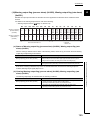
1
SAFETY PRECAUTIONS
(Read these precautions before using this product.)
Before using this product, please read this manual and the relevant manuals carefully and pay full attention
to safety to handle the product correctly.
The precautions given in this manual are concerned with this product only. For the safety precautions of the
programmable controller system, refer to the user’s manual for the CPU module used.
In this manual, the safety precautions are classified into two levels: "
WARNING" and "
CAUTION".
WARNING
Indicates that incorrect handling may cause hazardous conditions,
resulting in death or severe injury.
CAUTION
Indicates that incorrect handling may cause hazardous conditions,
resulting in minor or moderate injury or property damage.
Under some circumstances, failure to observe the precautions given under “
CAUTION” may lead to
serious consequences.
Observe the precautions of both levels because they are important for personal and system safety.
Make sure that the end users read this manual and then keep the manual in a safe place for future
reference.
[Design Precautions]
WARNING
● Do not write any data to the "system area" and "write-protect area" (R) of the buffer memory in the
intelligent function module.
Also, do not use any “use prohibited” signals as an output signal from the programmable controller
CPU to the intelligent function module.
Doing so may cause malfunction of the programmable controller system.
[Design Precautions]
CAUTION
● Do not install the control lines or communication cables together with the main circuit lines or power
cables. Keep a distance of 100mm or more between them. Failure to do so may result in malfunction
due to noise.
[Installation Precautions]
WARNING
● Shut off the external power supply (all phases) used in the system before mounting or removing a
module. Failure to do so may result in electric shock or cause the module to fail or malfunction.
1
[Installation Precautions]
CAUTION
● Use the programmable controller in an environment that meets the general specifications in the Safety
Guidelines provided with the CPU module or head module. Failure to do so may result in electric
shock, fire, malfunction, or damage to or deterioration of the product.
● To interconnect modules, engage the respective connectors and securely lock the module joint levers
until they click. Incorrect interconnection may cause malfunction, failure, or drop of the module.
● Tighten the screws within the specified torque range. Undertightening can cause drop of the screw,
short circuit, or malfunction. Overtightening can damage the screw and/or module, resulting in drop,
short circuit, or malfunction.
● Do not directly touch any conductive parts and electronic components of the module. Doing so can
cause malfunction or failure of the module.
[Wiring Precautions]
WARNING
● After installation and wiring, attach the included terminal cover to the module before turning it on for
operation. Failure to do so may result in electric shock.
[Wiring Precautions]
CAUTION
● Tighten the terminal block screws within the specified torque range. Undertightening can cause short
circuit, fire, or malfunction. Overtightening can damage the screw and/or module, resulting in drop,
short circuit, or malfunction.
● Prevent foreign matter such as dust or wire chips from entering the module. Such foreign matter can
cause a fire, failure, or malfunction.
● A protective film is attached to the top of the module to prevent foreign matter, such as wire chips,
from entering the module during wiring. Do not remove the film during wiring. Remove it for heat
dissipation before system operation.
● Mitsubishi programmable controllers must be installed in control panels. Connect the main power
supply to the power supply module in the control panel through a relay terminal block. Wiring and
replacement of a power supply module must be performed by qualified maintenance personnel with
knowledge of protection against electric shock. For wiring methods, refer to the MELSEC-L CPU
Module User's Manual (Hardware Design, Maintenance and Inspection).
[Startup and Maintenance Precautions]
WARNING
● Do not touch any terminal while power is on. Doing so will cause electric shock or malfunction.
● Shut off the external power supply (all phases) used in the system before cleaning the module or
retightening the terminal block screws. Failure to do so may result in electric shock.
2
[Startup and Maintenance Precautions]
CAUTION
● Do not disassemble or modify the module. Doing so may cause failure, malfunction, injury, or a fire.
● Shut off the external power supply (all phases) used in the system before mounting or removing a
module. Failure to do so may cause the module to fail or malfunction.
● Tighten the terminal block screws within the specified torque range. Undertightening can cause drop
of the screw, short circuit, or malfunction. Overtightening can damage the screw and/or module,
resulting in drop, short circuit, or malfunction.
● After the first use of the product (module, display unit, and terminal block), do not connect/disconnect
the product more than 50 times (in accordance with IEC 61131-2). Exceeding the limit may cause
malfunction.
● Before handling the module, touch a conducting object such as a grounded metal to discharge the
static electricity from the human body. Failure to do so may cause the module to fail or malfunction.
[Disposal Precautions]
CAUTION
● When disposing of this product, treat it as industrial waste.
3
CONDITIONS OF USE FOR THE PRODUCT
(1) Mitsubishi programmable controller ("the PRODUCT") shall be used in conditions;
i) where any problem, fault or failure occurring in the PRODUCT, if any, shall not lead to any major
or serious accident; and
ii) where the backup and fail-safe function are systematically or automatically provided outside of
the PRODUCT for the case of any problem, fault or failure occurring in the PRODUCT.
(2) The PRODUCT has been designed and manufactured for the purpose of being used in general
industries. MITSUBISHI SHALL HAVE NO RESPONSIBILITY OR LIABILITY (INCLUDING, BUT
NOT LIMITED TO ANY AND ALL RESPONSIBILITY OR LIABILITY BASED ON CONTRACT,
WARRANTY, TORT, PRODUCT LIABILITY) FOR ANY INJURY OR DEATH TO PERSONS OR
LOSS OR DAMAGE TO PROPERTY CAUSED BY the PRODUCT THAT ARE OPERATED OR
USED IN APPLICATION NOT INTENDED OR EXCLUDED BY INSTRUCTIONS, PRECAUTIONS,
OR WARNING CONTAINED IN MITSUBISHI'S USER, INSTRUCTION AND/OR SAFETY
MANUALS, TECHNICAL BULLETINS AND GUIDELINES FOR the PRODUCT. ("Prohibited
Application")
• Nuclear Power Plants and any other power plants operated by Power companies, and/or any
other cases in which the public could be affected if any problem or fault occurs in the PRODUCT.
• Railway companies or Public service purposes, and/or any other cases in which establishment of
a special quality assurance system is required by the Purchaser or End User.
• Aircraft or Aerospace, Medical applications, Train equipment, transport equipment such as
Elevator and Escalator, Incineration and Fuel devices, Vehicles, Manned transportation,
Equipment for Recreation and Amusement, and Safety devices, handling of Nuclear or
Hazardous Materials or Chemicals, Mining and Drilling, and/or other applications where there is a
significant risk of injury to the public or property.
Notwithstanding the above, restrictions Mitsubishi may in its sole discretion, authorize use of the
PRODUCT in one or more of the Prohibited Applications, provided that the usage of the PRODUCT
is limited only for the specific applications agreed to by Mitsubishi and provided further that no
special quality assurance or fail-safe, redundant or other safety features which exceed the general
specifications of the PRODUCTs are required. For details, please contact the Mitsubishi
representative in your region.
4
INTRODUCTION
Thank you for purchasing the Mitsubishi MELSEC-L series programmable controllers.
This manual describes the functions and programming of the multiple input (voltage/current/temperature) module.
Before using this product, please read this manual and the relevant manuals carefully and develop familiarity with the
functions and performance of the MELSEC-L series programmable controller to handle the product correctly.
When applying the program examples introduced in this manual to an actual system, ensure the applicability and
confirm that it will not cause system control problems.
Relevant module: L60MD4-G
Remark
● Unless otherwise specified, this manual describes the program examples in which the I/O numbers of X/Y00 to X/Y0F are
assigned for a multiple input module.
For I/O number assignment, refer to the following.
MELSEC-L CPU Module User's Manual (Function Explanation, Program Fundamentals)
● Operating procedures are explained using GX Works2. When using GX Developer, refer to the following.
• When Using GX Developer (
Page 171, Appendix 6)
5
COMPLIANCE WITH EMC AND LOW VOLTAGE
DIRECTIVES
(1) Method of ensuring compliance
To ensure that Mitsubishi programmable controllers maintain EMC and Low Voltage Directives when incorporated
into other machinery or equipment, certain measures may be necessary. Please refer to one of the following
manuals.
•
MELSEC-L CPU Module User's Manual (Hardware Design, Maintenance and Inspection)
•
MELSEC-L CC-Link IE Field Network Head Module User's Manual
• Safety Guidelines (This manual is included with the CPU module or head module.)
The CE mark on the side of the programmable controller indicates compliance with EMC and Low Voltage
Directives.
(2) Additional measures
No additional measures are necessary for the compliance of this product with the EMC and Low Voltage
Directives.
6
RELEVANT MANUALS
(1) CPU module user’s manual
Manual name
manual number (model code)
Description
MELSEC-L CPU Module User's Manual (Hardware Design, Maintenance
and Inspection)
SH-080890ENG, 13JZ36
Specifications of the CPU modules, power supply modules, display unit, branch
module, extension module, SD memory cards, and batteries, information on
how to establish a system, maintenance and inspection, and troubleshooting
MELSEC-L CPU Module User's Manual (Function Explanation, Program
Fundamentals)
SH-080889ENG, 13JZ35
Functions and devices of the CPU module, and programming
(2) Head module User’s Manual
Manual name
manual number (model code)
Description
MELSEC-L CC-Link IE Field Network Head Module User's Manual
SH-080919ENG, 13JZ48
Specifications, procedures before operation, system configuration, installation,
wiring, settings, and troubleshooting of the head module
(3) Operating manual
Manual name
manual number (model code)
Description
GX Works2 Version 1 Operating Manual (Common)
SH-080779ENG, 13JU63
System configuration, parameter settings, and online operations of GX Works2,
which are common to Simple projects and Structured projects
GX Developer Version 8 Operating Manual
Operating methods of GX Developer, such as programming, printing,
monitoring, and debugging
SH-080373E, 13JU41
7
CONTENTS
CONTENTS
SAFETY PRECAUTIONS . . . . . . . . . . . . . . . . . . . . . . . . . . . . . . . . . . . . . . . . . . . . . . . . . . . . . . . . . . . . . 1
CONDITIONS OF USE FOR THE PRODUCT . . . . . . . . . . . . . . . . . . . . . . . . . . . . . . . . . . . . . . . . . . . . . 4
INTRODUCTION . . . . . . . . . . . . . . . . . . . . . . . . . . . . . . . . . . . . . . . . . . . . . . . . . . . . . . . . . . . . . . . . . . . . 5
COMPLIANCE WITH EMC AND LOW VOLTAGE DIRECTIVES . . . . . . . . . . . . . . . . . . . . . . . . . . . . . . . 6
RELEVANT MANUALS . . . . . . . . . . . . . . . . . . . . . . . . . . . . . . . . . . . . . . . . . . . . . . . . . . . . . . . . . . . . . . . 7
MANUAL PAGE ORGANIZATION . . . . . . . . . . . . . . . . . . . . . . . . . . . . . . . . . . . . . . . . . . . . . . . . . . . . . . 11
TERMS . . . . . . . . . . . . . . . . . . . . . . . . . . . . . . . . . . . . . . . . . . . . . . . . . . . . . . . . . . . . . . . . . . . . . . . . . . 13
PACKING LIST . . . . . . . . . . . . . . . . . . . . . . . . . . . . . . . . . . . . . . . . . . . . . . . . . . . . . . . . . . . . . . . . . . . . 14
CHAPTER 1 MULTIPLE INPUT MODULE
1.1
Application . . . . . . . . . . . . . . . . . . . . . . . . . . . . . . . . . . . . . . . . . . . . . . . . . . . . . . . . . . . . . . . . 15
1.2
Features . . . . . . . . . . . . . . . . . . . . . . . . . . . . . . . . . . . . . . . . . . . . . . . . . . . . . . . . . . . . . . . . . . 16
CHAPTER 2 PART NAMES
18
CHAPTER 3 SPECIFICATIONS
20
3.1
3.2
General Specifications . . . . . . . . . . . . . . . . . . . . . . . . . . . . . . . . . . . . . . . . . . . . . . . . . . . . . . . 20
Performance Specifications . . . . . . . . . . . . . . . . . . . . . . . . . . . . . . . . . . . . . . . . . . . . . . . . . . . 21
3.2.1
Number of parameter settings . . . . . . . . . . . . . . . . . . . . . . . . . . . . . . . . . . . . . . . . . . . . . . . . .23
3.3
Function List . . . . . . . . . . . . . . . . . . . . . . . . . . . . . . . . . . . . . . . . . . . . . . . . . . . . . . . . . . . . . . . 24
3.4
List of I/O Signals . . . . . . . . . . . . . . . . . . . . . . . . . . . . . . . . . . . . . . . . . . . . . . . . . . . . . . . . . . . 26
3.5
List of Buffer Memory Addresses . . . . . . . . . . . . . . . . . . . . . . . . . . . . . . . . . . . . . . . . . . . . . . . 27
CHAPTER 4 PROCEDURES BEFORE OPERATION
32
CHAPTER 5 SYSTEM CONFIGURATION
34
5.1
Overall System Configuration . . . . . . . . . . . . . . . . . . . . . . . . . . . . . . . . . . . . . . . . . . . . . . . . . . 34
5.2
Applicable System . . . . . . . . . . . . . . . . . . . . . . . . . . . . . . . . . . . . . . . . . . . . . . . . . . . . . . . . . . 35
5.3
Restrictions When Connected to a Head Module. . . . . . . . . . . . . . . . . . . . . . . . . . . . . . . . . . . 35
CHAPTER 6 INSTALLATION AND WIRING
36
6.1
Installation Environment and Installation Position . . . . . . . . . . . . . . . . . . . . . . . . . . . . . . . . . . 36
6.2
Terminal Block . . . . . . . . . . . . . . . . . . . . . . . . . . . . . . . . . . . . . . . . . . . . . . . . . . . . . . . . . . . . . 36
6.3
Wiring . . . . . . . . . . . . . . . . . . . . . . . . . . . . . . . . . . . . . . . . . . . . . . . . . . . . . . . . . . . . . . . . . . . . 39
6.4
External Wiring . . . . . . . . . . . . . . . . . . . . . . . . . . . . . . . . . . . . . . . . . . . . . . . . . . . . . . . . . . . . . 41
CHAPTER 7 VARIOUS SETTINGS
43
7.1
Adding a Module. . . . . . . . . . . . . . . . . . . . . . . . . . . . . . . . . . . . . . . . . . . . . . . . . . . . . . . . . . . . 43
7.2
Parameter Settings . . . . . . . . . . . . . . . . . . . . . . . . . . . . . . . . . . . . . . . . . . . . . . . . . . . . . . . . . . 44
7.3
Auto Refresh. . . . . . . . . . . . . . . . . . . . . . . . . . . . . . . . . . . . . . . . . . . . . . . . . . . . . . . . . . . . . . . 47
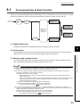
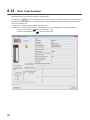
CHAPTER 8 FUNCTIONS
8.1
8
15
48
Processing Order of Each Function . . . . . . . . . . . . . . . . . . . . . . . . . . . . . . . . . . . . . . . . . . . . . 49
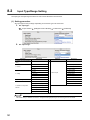
8.2
Input Type/Range Setting . . . . . . . . . . . . . . . . . . . . . . . . . . . . . . . . . . . . . . . . . . . . . . . . . . . . . 50
8.3
Conversion Method. . . . . . . . . . . . . . . . . . . . . . . . . . . . . . . . . . . . . . . . . . . . . . . . . . . . . . . . . . 53
8.4
Input Range Extension Function. . . . . . . . . . . . . . . . . . . . . . . . . . . . . . . . . . . . . . . . . . . . . . . . 57
8.5
Maximum Value/Minimum Value Hold Function . . . . . . . . . . . . . . . . . . . . . . . . . . . . . . . . . . . . 58
8.6
Disconnection Detection Function . . . . . . . . . . . . . . . . . . . . . . . . . . . . . . . . . . . . . . . . . . . . . . 59
8.7
Input Signal Error Detection Function. . . . . . . . . . . . . . . . . . . . . . . . . . . . . . . . . . . . . . . . . . . . 63
8.8
Warning Output Function . . . . . . . . . . . . . . . . . . . . . . . . . . . . . . . . . . . . . . . . . . . . . . . . . . . . . 70
8.9
Scaling Function . . . . . . . . . . . . . . . . . . . . . . . . . . . . . . . . . . . . . . . . . . . . . . . . . . . . . . . . . . . . 78
8.10
Error Log Function . . . . . . . . . . . . . . . . . . . . . . . . . . . . . . . . . . . . . . . . . . . . . . . . . . . . . . . . . . 84
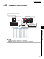
8.11
Module Error Collection Function . . . . . . . . . . . . . . . . . . . . . . . . . . . . . . . . . . . . . . . . . . . . . . . 87
8.12
Error Clear Function . . . . . . . . . . . . . . . . . . . . . . . . . . . . . . . . . . . . . . . . . . . . . . . . . . . . . . . . . 88
CHAPTER 9 DISPLAY UNIT
89
9.1
Display Unit. . . . . . . . . . . . . . . . . . . . . . . . . . . . . . . . . . . . . . . . . . . . . . . . . . . . . . . . . . . . . . . . 89
9.2
Menu Transition . . . . . . . . . . . . . . . . . . . . . . . . . . . . . . . . . . . . . . . . . . . . . . . . . . . . . . . . . . . . 89
9.3
List of Setting Value Change Windows. . . . . . . . . . . . . . . . . . . . . . . . . . . . . . . . . . . . . . . . . . . 92
9.4
Checking and Clearing Errors. . . . . . . . . . . . . . . . . . . . . . . . . . . . . . . . . . . . . . . . . . . . . . . . . 100
CHAPTER 10 PROGRAMMING
102
10.1
Programming Procedure. . . . . . . . . . . . . . . . . . . . . . . . . . . . . . . . . . . . . . . . . . . . . . . . . . . . . 102
10.2
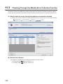
When Using the Module in a Standard System Configuration . . . . . . . . . . . . . . . . . . . . . . . . 103
10.3
When a Multiple Input Module Is Connected to a Head Module. . . . . . . . . . . . . . . . . . . . . . . 111
CHAPTER 11 TROUBLESHOOTING
121
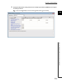
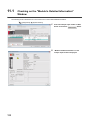
11.1
Checking on the "Module's Detailed Information" Window . . . . . . . . . . . . . . . . . . . . . . . . . . . 122
11.2
Checking in Latest Error Code (Un\G19) . . . . . . . . . . . . . . . . . . . . . . . . . . . . . . . . . . . . . . . . 123
11.3
Checking Through the Module Error Collection Function . . . . . . . . . . . . . . . . . . . . . . . . . . . . 124
11.4
List of Error Codes . . . . . . . . . . . . . . . . . . . . . . . . . . . . . . . . . . . . . . . . . . . . . . . . . . . . . . . . . 125
11.5
List of Alarm Codes . . . . . . . . . . . . . . . . . . . . . . . . . . . . . . . . . . . . . . . . . . . . . . . . . . . . . . . . 127
11.6
11.7
Troubleshooting . . . . . . . . . . . . . . . . . . . . . . . . . . . . . . . . . . . . . . . . . . . . . . . . . . . . . . . . . . . 128
11.6.1
Troubleshooting using LEDs . . . . . . . . . . . . . . . . . . . . . . . . . . . . . . . . . . . . . . . . . . . . . . . . .128
11.6.2
Troubleshooting for the conversion . . . . . . . . . . . . . . . . . . . . . . . . . . . . . . . . . . . . . . . . . . . .129
Checking the Multiple Input Module Status Using the System Monitor . . . . . . . . . . . . . . . . . 133
APPENDICES
134
Appendix 1 Details of I/O Signals. . . . . . . . . . . . . . . . . . . . . . . . . . . . . . . . . . . . . . . . . . . . . . . . . . . 134
Appendix 1.1
Input signal. . . . . . . . . . . . . . . . . . . . . . . . . . . . . . . . . . . . . . . . . . . . . . . . . . . . . . . . .134
Appendix 1.2
Output signal . . . . . . . . . . . . . . . . . . . . . . . . . . . . . . . . . . . . . . . . . . . . . . . . . . . . . . .139
Appendix 2 Details of Buffer Memory Addresses. . . . . . . . . . . . . . . . . . . . . . . . . . . . . . . . . . . . . . . 140
Appendix 3 I/O Conversion Characteristic of Voltage/Current . . . . . . . . . . . . . . . . . . . . . . . . . . . . . 161
Appendix 4 Accuracy . . . . . . . . . . . . . . . . . . . . . . . . . . . . . . . . . . . . . . . . . . . . . . . . . . . . . . . . . . . . 165
Appendix 5 How to Check the Function Version and Serial Number . . . . . . . . . . . . . . . . . . . . . . . . 169
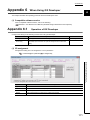
Appendix 6 When Using GX Developer . . . . . . . . . . . . . . . . . . . . . . . . . . . . . . . . . . . . . . . . . . . . . . 171
9
Appendix 6.1
Operation of GX Developer . . . . . . . . . . . . . . . . . . . . . . . . . . . . . . . . . . . . . . . . . . . .171
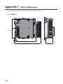
Appendix 7 External Dimensions . . . . . . . . . . . . . . . . . . . . . . . . . . . . . . . . . . . . . . . . . . . . . . . . . . . 172
INDEX
174
REVISIONS . . . . . . . . . . . . . . . . . . . . . . . . . . . . . . . . . . . . . . . . . . . . . . . . . . . . . . . . . . . . . . . . . . . . . . 176
WARRANTY . . . . . . . . . . . . . . . . . . . . . . . . . . . . . . . . . . . . . . . . . . . . . . . . . . . . . . . . . . . . . . . . . . . . . 177
TRADEMARKS . . . . . . . . . . . . . . . . . . . . . . . . . . . . . . . . . . . . . . . . . . . . . . . . . . . . . . . . . . . . . . . . . . . 178
10
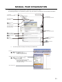
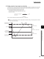
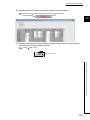
MANUAL PAGE ORGANIZATION
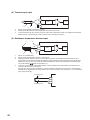
In this manual, pages are organized and the symbols are used as shown below.
The following illustration is for explanation purpose only, and should not be referred to as an actual documentation.
"" is used for
window names and items.
The chapter of
the current page is shown.
shows operating
procedures.
shows mouse
operations.*1
[ ] is used for items
in the menu bar and
the project window.
The section of
the current page is shown.
Ex. shows setting or
operating examples.
shows reference
manuals.
shows
reference pages.
shows notes that
require attention.
shows useful
information.
*1
The mouse operation example (for GX Works2) is provided below.
Menu bar
Ex.
[Online]
[Write to PLC...]
Select [Online] on the menu bar,
and then select [Write to PLC...].
A window selected in the view selection area is displayed.
Ex.
[Parameter]
Project window
[PLC Parameter]
Select [Project] from the view selection
area to open the Project window.
In the Project window, expand [Parameter] and
select [PLC Parameter].
View selection area
11
Pages describing the functions, I/O signals, and buffer memory areas are organized as shown below.
The following illustration is for explanation purpose only, and should not be referred to as an actual documentation.
Each icon indicates the available input type.
Most of the functions in this module are commonly available regardless of the input type, but some of them may not be
available depending on the input type.
Each icon indicates an input type that allows the use of the function, I/O signal, and buffer memory area.
12
TERMS
Unless otherwise specified, this manual uses the following terms.
Term
Description
Multiple input
A capability to input analog signals by different input types (voltage, current, micro voltage, resistance temperature
detector, and thermocouple) for one channel
Multiple input module
Abbreviation for the MELSEC-L series multiple input (voltage/current/temperature) module
Head module
Abbreviation for the LJ72GF15-T2 CC-Link IE Field Network head module
Display unit
A liquid crystal display to be attached to the CPU module
Programming tool
A generic term for GX Works2 and GX Developer
GX Works2
GX Developer
The product name of the software package for the MELSEC programmable controllers
Input type
A type of analog signals (voltage, current, and a sensor such as a thermocouple and a resistance temperature detector)
to be input to the multiple input module from the outside
Input range
A property that indicates the range of input value when the input type is set to the voltage, current, or micro voltage;
indicates the type of resistance temperature detector when the input type is set to the resistance temperature detector;
indicates the type of thermocouple when the input type is set to the thermocouple
Conversion
A generic term for processing of converting an analog signal, such as voltage and current, into a digital value, and
processing of converting a resistance value and thermoelectromotive force value, which are measured by the resistance
temperature detector and thermocouple respectively, into a temperature measured value
Digital output value
A generic term for digital values and temperature measured values converted from analog signals which have been input
from the outside
Conversion disabled
Conversion enabled
The state that Disable Conversion (0000H) is set in CH Input type/range setting (Un\G500 to Un\G503). In this state,
the conversion is not performed on the corresponding channel.
The state that the input type and input range suitable to the type of sensor connected (value other than Disable
conversion (0000H)) are set in CH Input type/range setting (Un\G500 to Un\G503). In this state, the conversion is
performed on the corresponding channel.
Buffer memory
A memory in an intelligent function module, where data (such as setting values and monitoring values) exchanged with a
CPU module are stored
Watchdog timer error
An error that occurs if the internal processing of the multiple input module fails. The module monitors its own internal
processing by using the watchdog timer.
13
PACKING LIST
The following items are included in the package of this product. Before use, check that all the items are included.
L60MD4-G
Before Using the Product
L60MD4-G
Cold junction compensation resistor
14
CHAPTER 1 MULTIPLE INPUT MODULE
CHAPTER 1
MULTIPLE INPUT MODULE
1
This chapter describes the applications and features of the multiple input module.
1.1
Application
With the multiple input module, analog signals can be input in five input types: voltage, current, micro voltage,
resistance temperature detector, and thermocouple. Also, an input type can be selected for each channel depending
on the type of the object to be measured.
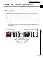
With the multiple input module, the following applications are possible.
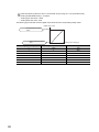
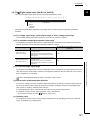
(1) Reducing the cost for the system
Since different types of sensors can be connected to each channel individually, dedicated modules prepared for
each type of sensors can be integrated in one module. Thus, the space and cost for the system can be saved. In
addition, the types and quantity of spare items used for module failures can be reduced, reducing the
maintenance cost.
For the system in which the number of channels used for the analog input and temperature input is four
channels or less
⋅
Conventional system
System using the multiple input module
+
+
Voltage/current input, thermocouple input,
resistance temperature detector input: L60MD4-G (4CH)
+
+
+
1.1 Application
⋅ Voltage/current input: L60AD4 (4CH)
⋅ Thermocouple input: L60TCTT4 (4CH)
⋅ Resistance temperature detector input: L60TCRT4 (4CH)
+
Cost reduction is
achieved by reducing wasteful
use of channels.
15
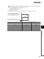
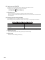
(2) Shortening the system development period
Since the multiple input module can be connected to sensors of different types, the module can be prepared
before sensors are selected. Since the system can be started earlier than before, the time required for the system
operation can be shortened.
Selecting sensors
Arranging for modules
Starting up the system
Cut-back period
Selecting sensors
Starting up the system
Arranging for modules
The early
arrangement for modules
results in an earlier starting
time for system
operation.
(3) Supporting conventional standard sensors
The multiple input module supports Pt50 and JPt100. Thus, when the equipment using the sensors of Pt50 and
JPt100 is updated, the sensors do not need to be changed.
1.2
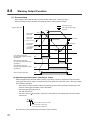
Features
(1) Scale conversion
This function converts a digital output value to the ratio value (%) in any width to represent the digital value in a
numeric value easy to understand.
(2) Comparing and monitoring an object
The status of the connected device can be easily monitored by using the disconnection detection function (or
input signal error detection function), input range extension function, and warning output function (process alarms
and rate alarms).
(3) Switching the Celsius/Fahrenheit display
For the temperature input (thermocouples and resistance temperature detectors), the Celsius/Fahrenheit display
of the temperature measured value can be easily switched.
16
CHAPTER 1 MULTIPLE INPUT MODULE
1
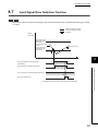
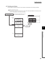
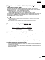
(4) Stable measurement due to the isolation between channels
Channels are isolated, and this eliminates noises from other channels to stable the measurement.
Multiple input module
Sensor
CH1
V+
V-
A/D
conversion
CH2
V+
V-
A/D
conversion
CH3
V+
V-
A/D
conversion
CH4
V+
V-
A/D
conversion
Isolation between channels
Isolation between channels
prevents wrap-around noise
between channels.
(5) Easy setting with GX Works2
Programming is reduced because the initial settings or auto refresh settings can be set on the screen. In addition,
setting status and operating status of modules can be checked easily.
1.2 Features
17
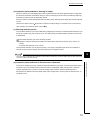
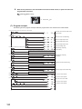
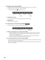
CHAPTER 2
PART NAMES
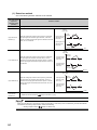
The following table shows part names of the multiple input module.
1)
1)
4)
2)
3)
9)
7)
6)
5)
1)
No.
8)
1)
Name
Description
1)
Module joint levers
Levers for connecting modules
2)
RUN LED (green)
Indicates the operating status of the multiple input module.
On: The module is operating normally.
Off: The 5V power off or watchdog timer error has occurred.
3)
ERR. LED (red)
Indicates the error status of the multiple input module.
On: An error has occurred.*1
Off: The module is operating normally.
Indicates the alarm occurrence of the multiple input module.
On: A warning (process alarm, rate alarm) has occurred.*2
Flashing: Indicates either of the following statuses.
4)
ALM LED (red)
• A disconnection is detected.*2
• An input signal error has been detected.*2
• The thermocouple is selected for the input type and the cold junction compensation resistor (CJ) is
not connected to CH1.*4
Off: The module is operating normally.
18
5)
DIN rail hook
A hook used to mount the module to a DIN rail
6)
Terminal block*3
A 18-point screw terminal block for connecting input signal lines of external devices
7)
Terminal block cover
A cover for preventing electric shock while the power is on
8)
Serial number display
Displays the serial number printed on the rating plate.
9)
Cold junction compensation resistor
A resistance temperature detector used for the cold junction compensation. Connect this resister to
CH1 when the thermocouple is selected for the input type.
*1
For details on the list of error codes, refer to the following. (
Page 125, Section 11.4)
*2
For details on the list of alarm codes, refer to the following. (
*3
For the signal assignment for the terminal block, refer to the following. (
*4
For details on wiring, refer to the following. (
Page 127, Section 11.5)
Page 39, Section 6.3)
Page 37, Section 6.2 (2))
CHAPTER 2 PART NAMES
Memo
2
19
CHAPTER 3
SPECIFICATIONS
This chapter describes general specifications, performance specifications, function list, list of I/O signals, and list of
buffer memory addresses.
3.1
General Specifications
For the general specifications of the multiple input module, refer to the following.
The manual "Safety Guidelines" included with the CPU module or head module
20
CHAPTER 3 SPECIFICATIONS
3.2
Performance Specifications
The following table lists the performance specifications of the multiple input module.
Model
Item
Number of analog input points
Analog input
3
Voltage
-10 to 10VDC (input resistance 1M)
Current
0 to 20mADC (input resistance 250)
Micro voltage
-100 to 100mVDC
Thermocouple
Resistance temperature
detector
Digital output value
Digital output
When using the scaling
function
Available type
12 types
K, J, T, E, N, R, S, B, U, L, PLII, W5Re/W26Re
Cold junction compensation
resistor
Use the included cold junction compensation resistor (CJ).
Available type
4 types
Pt1000, Pt100, JPt100, Pt50
Measurement method
3-wire system
Voltage, current, micro voltage
-20480 to 20479
Resistance temperature detector
Pt100 (-20 to 120°C), JPt100 (-20
to 120°C)
• For Celsius: -2000 to 12000*1
• For Fahrenheit: 0 to 20000
Value rounded off to two decimal places × 100 times
Thermocouple,
Resistance temperature detector
(other than the above)
• For Celsius: -2700 to 23000*1
• For Fahrenheit: -4000 to 32000
Value rounded off to one decimal place × 10 times
-32768 to 32767
Analog input range
Digital output value
Resolution
0 to 10V
0 to 20000
500µV
0 to 5V
0 to 20000
250µV
1 to 5V
0 to 20000
200µV
-10 to 10V
-20000 to 20000
500µV
1 to 5V (extended mode)
-5000 to 22500
200µV
0 to 20mA
Resolution
Current
4 to 20mA
0 to 20000
1000nA
800nA
4 to 20mA (extended mode)
-5000 to 22500
800nA
Micro voltage
-100 to 100mV
-20000 to 20000
5µV
Thermocouple*2
B, R, S, N, PLII, W5Re/W26Re: 0.3°C
K, E, J, T, U, L: 0.1°C
Resistance temperature
detector*3
Pt100 (-20 to 120°C), JPt100 (-20 to 120°C): 0.03°C
Pt100 (-200 to 850°C), JPt100 (-200 to 600°C), Pt1000, Pt50: 0.1°C
Voltage/current/micro
voltage
Ambient temperature 25±5°C
Maximum value of the measurement range × (±0.3%) (±60 digits)
Ambient temperature 0 to 55°C
Maximum value of the measurement range × (±0.9%) (±180 digits)
Thermocouple
(For details, refer to the
Ambient temperature 25±5°C
Full scale × (±0.15%)
following. (
Page
166, Appendix 4 (2)))
Ambient temperature 0 to 55°C
Full scale × (±0.3%)*8
Temperature measured value: 100°C or higher
Within ±1.0°C
Temperature measured value:
-150°C to -100°C
Within ±2.0°C
Temperature measured value:
-200°C to -150°C
Within ±3.0°C
Accuracy
*4*7
Cold junction
compensation resistor*9
Resistance temperature
detector
3.2 Performance Specifications
Voltage
Conversion speed
L60MD4-G
4 points (4 channels)
Page 168, Appendix 4 (3)
50ms/channel
21
Model
Item
L60MD4-G
Temperature detecting output current
Pt100, JPt100, Pt50: 1mA, Pt1000: 0.2mA
Absolute maximum input
Voltage: ±15V, Current: 30mA*5
Insulation method
Between input terminals and programmable controller power supply: Photocoupler
Between input channels: Transformer
Dielectric withstand voltage
Between input terminals and programmable controller power supply: 500VACrms for 1 minute
Between input channels: 500VACrms for 1 minute
Insulation resistance
Between input terminals and programmable controller power supply: 500VDC 10M or higher
Between input channels: 500VDC 10M or higher
Disconnection detection
Available*6
Number of occupied I/O points
16 points (I/O assignment: Intelligent 16 points)
Connected terminal
18-point terminal block
Applicable wire size
0.3 to 0.75mm2
Applicable solderless terminal
R1.25-3 (solderless terminals with sleeve are not usable)
Internal current consumption (5VDC)
0.49A
Weight
0.19kg
*1
This manual describes the temperature in Celsius. To read the temperature in Fahrenheit, refer to the following.
*2
• Accuracy for when a thermocouple is connected (
Page 166, Appendix 4 (2))
• Accuracy for when a resistance temperature detector is connected (
Page 168, Appendix 4 (3))
For the temperature measuring range of each thermocouple, refer to the following.
*3
• Accuracy for when a thermocouple is connected (
Page 166, Appendix 4 (2))
For the temperature measuring range of each resistance temperature detector, refer to the following.
*4
*5
*6
*7
*8
*9
• Accuracy for when a resistance temperature detector is connected (
Page 168, Appendix 4 (3))
Except when receiving noise influence.
A momentary current value which does not cause damage to internal resistors of the module. The maximum input
current value for constant application is 24mA.
When the input type in CH Input type/range setting (Un\G500 to Un\G503) is a resistance temperature detector,
thermocouple, or micro voltage, a disconnection of the connected signal line can be detected. Also, when the input
range is 4 to 20mA (extended mode) or 1 to 5V (extended mode), the simple disconnection detection can be executed
using the input signal error detection function.
For details on the disconnection detection function and input signal error detection function, refer to the following.
• Disconnection Detection Function (
Page 59, Section 8.6)
• Input Signal Error Detection Function (
Page 63, Section 8.7)
To acquire sufficient accuracy, a warm-up (conduction) for 15 minutes is required.
The accuracy for when the measured temperature of the type W5Re/W26Re thermocouple is 2000°C or higher is
±0.5%.
The following table shows the accuracy of the cold junction compensation for when the type T thermocouple or type U
thermocouple is used.
Measured temperature
22
Type T thermocouple
0°C or higher
±1.0°C
-100°C to 0°C
±2.0°C
-150°C to -100°C
±3.0°C
-200°C to -150°C
±5.0°C
Type U thermocouple
±4.0°C
CHAPTER 3 SPECIFICATIONS
3.2.1
Number of parameter settings
Set the initial settings of the multiple input module and the parameter settings of the auto refresh setting so that the
number of parameters, including those of other intelligent function modules, does not exceed the number of
parameters that can be set in a CPU module.
For the maximum number of parameters that can be set in a CPU module (maximum number of parameter settings),
3
refer to the following.
MELSEC-L CPU Module User's Manual (Hardware Design, Maintenance and Inspection)
MELSEC-L CC-Link IE Field Network Head Module User's Manual
(1) Number of parameters of the multiple input module
The following number of parameters can be set in a single multiple input module.
Target module
Initial setting
L60MD4-G
Auto refresh setting
8
23 (maximum)
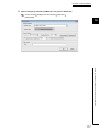
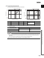
(2) Checking method
The maximum number of the parameter settings and the number of the parameter settings set for an intelligent
function module can be checked with the following operation.
Project window
[Intelligent Function Module]
Right-click
[Intelligent Function Module
Parameter List]
3.2 Performance Specifications
1)
No.
2)
3)
4)
Description
1)
The total number of the parameters in the initial settings selected on the window
2)
The maximum number of the parameter settings in the initial settings
3)
The total number of the parameters in the auto refresh settings selected on the window
4)
The maximum number of the parameter settings in the auto refresh settings
23
3.3
Function List
The following table lists the functions of the multiple input module.
Item
Description
Reference
Temperature conversion function
By connecting a thermocouple or resistance temperature detector, the temperature data
can be imported.
-
Celsius/Fahrenheit display switching
function
Celsius or Fahrenheit can be selected as the display unit of the temperature measured
value imported using the temperature conversion function.
Page 157,
Appendix 2 (22)
Voltage/current/micro voltage conversion
function
A voltage of -10 to 10V, current of 0 to 20mA, and micro voltage of -100 to 100mV are
converted and stored in the buffer memory.
-
Input type/range setting
The input type and input range that are to be used can be selected for each channel.
Disabling the conversion for unused channels reduces the conversion cycles.
Page 50, Section
8.2
Analog input values and temperature input values are converted at every sampling cycle
and stored in the buffer memory as digital output values.
Page 53, Section
8.3 (1)
Time
average
The conversion is performed for a set period of time and averaging processing is
performed on the total value excluding the maximum and minimum values. The values
obtained in averaging processing are stored in the buffer memory. The number of
processing times within a set period of time changes depending on the number of
channels where the conversion is enabled.
Page 53, Section
8.3 (2) (a)
Count
average
The conversion is performed a set number of times and averaging processing is performed
on the total value excluding the maximum and minimum values. The values obtained in
averaging processing are stored in the buffer memory. The time taken to store the average
value obtained by the average processing in the buffer memory area changes depending
on the number of channels where the conversion is enabled.
Page 54, Section
8.3 (2) (b)
Moving
average
The average of a specified number of digital output values is calculated at every sampling
cycle and is stored in the buffer memory. Because the target range for averaging
processing is moved in response to every sampling processing, the latest digital output
value can be obtained.
Page 55, Section
8.3 (2) (c)
Input range extension function
This function extends the input range of 4 to 20mA and that of 1 to 5V. In combination with
the input signal error detection function, this function allows a simple disconnection
detection.
Page 57, Section
8.4
Maximum value/minimum value hold
function
This function stores the maximum digital value and minimum digital output value in the
buffer memory for each channel. When the scaling function is used, the maximum scaling
value and minimum scaling value are stored.
Page 58, Section
8.5
Disconnection detection function
This function outputs an alarm at disconnection detection of the external wiring, provided
that the input type is a thermocouple, resistance temperature detector, or micro voltage.
The digital output value at the disconnection detection can be selected from the following
values.
• Value just before disconnection
• Up scale
• Down scale
• Optional value
Page 59, Section
8.6
Input signal error detection function
This function outputs an alarm at the time when an analog input value exceeds a preset
range, provided that the input type is voltage or current.
Page 63, Section
8.7
Process alarm
When a digital output value falls within a preset warning output range, a warning is output.
With the scaling function used, the scaling value is the warning detection target.
Page 70, Section
8.8 (1)
Rate alarm
When the change rate of a digital output value is larger than the rate alarm upper limit
value or smaller than the rate alarm lower limit value, a warning is output.
Page 72, Section
8.8 (2)
Scaling function
This function performs the scale conversion on digital output values. The values are
converted within the range between a specified scaling upper limit value and scaling lower
limit value. This function reduces the time and effort to create a program of the scale
conversion.
Page 78, Section
8.9
Error log function
This function stores the errors and alarms that occurred in the multiple input module in the
buffer memory area.
A total of 16 errors and alarms can be stored.
Page 84, Section
8.10
Module error collection function
This function collects the errors and alarms that occurred in the multiple input module and
stores them in the CPU module.
Page 87, Section
8.11
Error clear function
This function allows clearing of errors through the system monitor at the occurrence of an
error.
Page 88, Section
8.12
Sampling processing
Conversion
method
Warning output
function
24
Averaging
processing
CHAPTER 3 SPECIFICATIONS
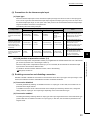
(1) Correspondence between the disconnection detection function/input signal
error detection function and each input type/input range
Depending on the input type and input range used, the disconnection detection function or input signal error
detection function can be used.
Input type
Input range
Disconnection
detection
function
Input signal error detection function
Upper and
lower detection
4 to 20mA
Current
0 to 20mA
Lower
detection
Upper
detection
Simple
disconnection
detection
3
×
×
4 to 20mA (extended mode)
1 to 5V
0 to 5V
Voltage
-10 to 10V
×
×
0 to 10V
1 to 5V (extended mode)
Micro voltage
-100 to 100mV
×
Resistance
temperature
detector
Common to all input ranges
×
Thermocouple
Common to all input ranges
×
3.3 Function List
25
3.4
List of I/O Signals
The following table lists the I/O signals of the multiple input module.
For details of the I/O signals, refer to the following.
• Details of I/O Signals (
Page 134, Appendix 1)
Input signal
Device number
X0
Output signal
Signal name
Module READY
X1
Y2
Use prohibited
Y3
X4
Y4
X5
Y5
X6
Disconnection detection signal
Y6
X7
Use prohibited
Y7
X8
Warning output signal
Y8
X9
Operating condition setting completed flag
XA
XB
Signal name
Y0
Y1
X2
X3
Device number
Use prohibited
Y9
Use prohibited
Operating condition setting request
YA
YB
Use prohibited
XC
Input signal error detection signal
YC
XD
Maximum value/minimum value reset completed
flag
YD
Maximum value/minimum value reset request
XE
Conversion completed flag
YE
Use prohibited
XF
Error flag
YF
Error clear request
● The I/O number (X/Y) described above shows the case that the start I/O number of the multiple input module is set to "0".
● Do not use the "Use prohibited" signals shown above because the system uses them.
If users use (turn on) the signals, the functions of the multiple input module cannot be guaranteed.
26
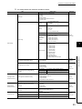
CHAPTER 3 SPECIFICATIONS
3.5
List of Buffer Memory Addresses
The following table lists the buffer memory addresses of the multiple input module.
For details of the buffer memory, refer to the following.
• Details of Buffer Memory Addresses (
Page 140, Appendix 2)
3
Do not write data to the system areas and read-only areas in the buffer memory.
Writing data to these areas may cause malfunction of the module.
(1) Un\G0 to Un\G1799
Address
(decimal)
Address
(hexadecimal)
Default
Name
Read/Write
value*1
Item enabled by
turning on and off
Operating condition
setting request (Y9)
*2
0
0H
System area
-
-
1
1H
CH1 Time Average/Count Average/Moving Average
0
R/W
2
2H
CH2 Time Average/Count Average/Moving Average
0
R/W
3
3H
CH3 Time Average/Count Average/Moving Average
0
R/W
4
4H
CH4 Time Average/Count Average/Moving Average
0
R/W
5 to 9
5H to 9H
System area
-
-
-
10
AH
Conversion completed flag
0000H
R
-
11
BH
CH1 Digital output value
0
R
-
12
CH
CH2 Digital output value
0
R
-
13
DH
CH3 Digital output value
0
R
-
14
EH
CH4 Digital output value
0
R
-
-
FH to 12H
System area
-
-
-
13H
Latest error code
0
R
-
20 to 23
14H to 17H
System area
-
-
-
24
18H
Averaging process setting
0000H
R/W
25 to 29
19H to 1DH
System area
-
-
30
1EH
CH1 Maximum value
0
R
-
31
1FH
CH1 Minimum value
0
R
-
32
20H
CH2 Maximum value
0
R
-
33
21H
CH2 Minimum value
0
R
-
34
22H
CH3 Maximum value
0
R
-
35
23H
CH3 Minimum value
0
R
-
36
24H
CH4 Maximum value
0
R
-
37
25H
CH4 Minimum value
0
R
-
38 to 46
26H to 2EH
System area
-
-
-
47
2FH
Disconnection detection flag
0000H
R
-
48
30H
Warning output setting
0F0FH
R/W
49
31H
Input signal error detection flag
0000H
R
-
50
32H
Warning output flag (process alarm)
0000H
R
-
51
33H
Warning output flag (rate alarm)
0000H
R
-
52
34H
System area
-
-
-
3.5 List of Buffer Memory Addresses
15 to 18
19
-
27
Address
(decimal)
Address
(hexadecimal)
Default
Name
Item enabled by
turning on and off
Operating condition
setting request (Y9)
*2
Read/Write
value*1
53
35H
Scaling enable/disable setting
000FH
R/W
54
36H
CH1 Scaling value
0
R
-
55
37H
CH2 Scaling value
0
R
-
56
38H
CH3 Scaling value
0
R
-
57
39H
CH4 Scaling value
0
R
-
58 to 61
3AH to 3DH
System area
-
-
-
62
3EH
CH1 Scaling lower limit value
0
R/W
63
3FH
CH1 Scaling upper limit value
0
R/W
64
40H
CH2 Scaling lower limit value
0
R/W
65
41H
CH2 Scaling upper limit value
0
R/W
66
42H
CH3 Scaling lower limit value
0
R/W
67
43H
CH3 Scaling upper limit value
0
R/W
68
44H
CH4 Scaling lower limit value
0
R/W
69
45H
CH4 Scaling upper limit value
0
R/W
70 to 85
46H to 55H
System area
-
-
86
56H
CH1 Process alarm lower lower limit value
0
R/W
87
57H
CH1 Process alarm lower upper limit value
0
R/W
88
58H
CH1 Process alarm upper lower limit value
0
R/W
89
59H
CH1 Process alarm upper upper limit value
0
R/W
90
5AH
CH2 Process alarm lower lower limit value
0
R/W
91
5BH
CH2 Process alarm lower upper limit value
0
R/W
92
5CH
CH2 Process alarm upper lower limit value
0
R/W
93
5DH
CH2 Process alarm upper upper limit value
0
R/W
94
5EH
CH3 Process alarm lower lower limit value
0
R/W
95
5FH
CH3 Process alarm lower upper limit value
0
R/W
96
60H
CH3 Process alarm upper lower limit value
0
R/W
97
61H
CH3 Process alarm upper upper limit value
0
R/W
98
62H
CH4 Process alarm lower lower limit value
0
R/W
99
63H
CH4 Process alarm lower upper limit value
0
R/W
100
64H
CH4 Process alarm upper lower limit value
0
R/W
101
65H
CH4 Process alarm upper upper limit value
0
R/W
102 to 117
66H to 75H
System area
-
-
118
76H
CH1 Rate alarm detection cycle
0
R/W
119
77H
CH2 Rate alarm detection cycle
0
R/W
120
78H
CH3 Rate alarm detection cycle
0
R/W
121
79H
CH4 Rate alarm detection cycle
0
R/W
122 to 125
7AH to 7DH
System area
-
-
126
7EH
CH1 Rate alarm upper limit value
0
R/W
127
7FH
CH1 Rate alarm lower limit value
0
R/W
128
80H
CH2 Rate alarm upper limit value
0
R/W
129
81H
CH2 Rate alarm lower limit value
0
R/W
130
82H
CH3 Rate alarm upper limit value
0
R/W
28
-
-
-
CHAPTER 3 SPECIFICATIONS
Address
(decimal)
Address
(hexadecimal)
Default
Name
Read/Write
value*1
Item enabled by
turning on and off
Operating condition
setting request (Y9)
*2
131
83H
CH3 Rate alarm lower limit value
0
R/W
132
84H
CH4 Rate alarm upper limit value
0
R/W
133
85H
CH4 Rate alarm lower limit value
0
R/W
134 to 399
86H to 18FH
System area
-
-
400
190H
Conversion setting at disconnection detection
0000H
R/W
401
191H
System area
-
-
402
192H
Input signal error detection setting
0000H
R/W
403
193H
System area
-
-
404
194H
CH1 Conversion setting value at disconnection
detection
0
R/W
405
195H
CH2 Conversion setting value at disconnection
detection
0
R/W
406
196H
CH3 Conversion setting value at disconnection
detection
0
R/W
407
197H
CH4 Conversion setting value at disconnection
detection
0
R/W
408 to 411
198H to 19BH
System area
-
-
412
19CH
CH1 Input signal error detection setting value
50
R/W
413
19DH
CH2 Input signal error detection setting value
50
R/W
414
19EH
CH3 Input signal error detection setting value
50
R/W
415
19FH
CH4 Input signal error detection setting value
50
R/W
416 to 499
1A0H to 1F3H
System area
-
-
500
1F4H
CH1 Input type/range setting
0000H
R/W
501
1F5H
CH2 Input type/range setting
0000H
R/W
502
1F6H
CH3 Input type/range setting
0000H
R/W
503
1F7H
CH4 Input type/range setting
0000H
R/W
504 to 507
1F8H to 1FBH
System area
-
-
508
1FCH
CH1 Celsius/Fahrenheit display setting
0
R/W
509
1FDH
CH2 Celsius/Fahrenheit display setting
0
R/W
510
1FEH
CH3 Celsius/Fahrenheit display setting
0
R/W
511
1FFH
CH4 Celsius/Fahrenheit display setting
0
R/W
512 to 515
200H to 203H
System area
-
-
-
-
3
-
-
-
-
3.5 List of Buffer Memory Addresses
-
516
204H
CH1 Input type/range monitor
0000H
R
-
517
205H
CH2 Input type/range monitor
0000H
R
-
518
206H
CH3 Input type/range monitor
0000H
R
-
519
207H
CH4 Input type/range monitor
0000H
R
-
520 to 523
208H to 20BH
System area
-
-
-
524
20CH
CH1 Celsius/Fahrenheit monitor
0
R
-
525
20DH
CH2 Celsius/Fahrenheit monitor
0
R
-
526
20EH
CH3 Celsius/Fahrenheit monitor
0
R
-
527
20FH
CH4 Celsius/Fahrenheit monitor
0
R
-
528 to 1699
210H to 6A3H
System area
-
-
-
1700
6A4H
CH1 Conversion status
0
R
-
1701
6A5H
CH2 Conversion status
0
R
-
1702
6A6H
CH3 Conversion status
0
R
-
29
Address
(decimal)
Address
(hexadecimal)
1703
1704 to 1799
*1
*2
30
Default
Name
Item enabled by
turning on and off
Operating condition
setting request (Y9)
*2
Read/Write
value*1
6A7H
CH4 Conversion status
0
R
-
6A8H to 707H
System area
-
-
-
The default value is a value to be set after power-on or after resetting the CPU module.
This column shows whether or not data can be read or written through programs.
R: Readable
W: Writable
CHAPTER 3 SPECIFICATIONS
(2) Error history (Un\G1800 to Un\G61439)
Address
(decimal)
Address
(hexadecimal)
Default
Name
Item enabled by
turning on and off
Operating condition
setting request (Y9)
Read/Write*2
value*1
1800
708H
Latest address of error history
0
R
-
1801 to 1809
709H to 711H
System area
-
-
-
1810
712H
0
R
-
1811
713H
1812
714H
1813
715H
Error code
No.1
Error time
First two
digits of the
year
Last two
digits of the
year
0
R
-
Month
Day
0
R
-
Hour
Minute
0
R
-
Second
Day of the
week
0
R
-
-
-
-
716H
1815 to 1819
717H to 71BH
1820 to 1829
71CH to 725H
No.2
Same as No. 1
-
1830 to 1839
726H to 72FH
No.3
Same as No. 1
-
1840 to 1849
730H to 739H
No.4
Same as No. 1
-
1850 to 1859
73AH to 743H
No.5
Same as No. 1
-
1860 to 1869
744H to 74DH
No.6
Same as No. 1
-
1870 to 1879
74EH to 757H
No.7
Same as No. 1
-
1880 to 1889
758H to 761H
No.8
Same as No. 1
-
1890 to 1899
762H to 76BH
No.9
Same as No. 1
-
1900 to 1909
76CH to 775H
No.10
Same as No. 1
-
1910 to 1919
776H to 77FH
No.11
Same as No. 1
-
1920 to 1929
780H to 789H
No.12
Same as No. 1
-
1930 to 1939
78AH to 793H
No.13
Same as No. 1
-
1940 to 1949
794H to 79DH
No.14
Same as No. 1
-
1950 to 1959
79EH to 7A7H
No.15
Same as No. 1
-
1960 to 1969
7A8H to 7B1H
No.16
Same as No. 1
1970 to 61439
7B2H to EFFFH
System area
*1
*2
System area
3.5 List of Buffer Memory Addresses
1814
3
-
-
-
The default value is a value to be set after power-on or after resetting the CPU module.
This column shows whether or not data can be read or written through programs.
R: Readable
W: Writable
31
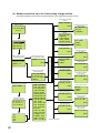
CHAPTER 4
PROCEDURES BEFORE OPERATION
This chapter describes the procedures before operation.
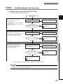
Start
Connecting a module
Connect a multiple input module in any desired
configuration.
Wiring
Perform wiring of external devices to the multiple
input module.
For details on the connection of modules, refer to the following.
•
Page 34, Section 5.1
For wiring, refer to the following.
Does thermocouple input need to be used?
Yes
Connect a cold junction compensation resistor to
CH1.
Programming and debugging
Create and check a program.
32
No
•
Page 41, Section 6.4
CHAPTER 4 PROCEDURES BEFORE OPERATION
Memo
4
33
CHAPTER 5
SYSTEM CONFIGURATION
This chapter describes the overall configuration, number of connectable modules, and compatible software version of
the multiple input module.
5.1
Overall System Configuration
The following figure shows system configuration examples for using the multiple input module.
(1) When connected to a CPU module
Display module
(optional)
Power supply
module
Multiple input
module
CPU module
I/O module
or
intelligent function module
END
cover
(2) When connected to a head module
Power supply
module
34
Head module
Multiple input
module
I/O module
or
intelligent function module
END cover
CHAPTER 5 SYSTEM CONFIGURATION
5.2
Applicable System
(1) Number of connectable modules
For the number of connectable modules, refer to the following.
MELSEC-L CPU Module User's Manual (Hardware Design, Maintenance and Inspection)
MELSEC-L CC-Link IE Field Network Head Module User's Manual
(2) Compatible software version
The following table shows the compatible software versions.
Software
Version
GX Works2
Version 1.513K or later
GX Developer
Version 8.88S or later
5
(3) Temperature sensor
For available temperature sensors, refer to the following.
Page 21, Section 3.2
5.3
Restrictions When Connected to a Head Module
When the multiple input module is used with the head module, function blocks (FBs) in MELSOFT Library cannot be
used.
5.2 Applicable System
35
CHAPTER 6
6.1
INSTALLATION AND WIRING
Installation Environment and Installation Position
For precautions for the installation environment and installation position, refer to the following.
MELSEC-L CPU Module User's Manual (Hardware Design, Maintenance and Inspection)
MELSEC-L CC-Link IE Field Network Head Module User's Manual
6.2
Terminal Block
(1) Precautions
Tighten the terminal block screws within the following specified torque range.
Screw type
Tightening torque range
Terminal screw (M3 screw)
0.42 to 0.58Nm
Terminal block mounting screw (M3.5 screw)
0.66 to 0.89Nm
The following table lists applicable solderless terminals to be connected to the terminal block. When wiring, use
applicable wires and an appropriate tightening torque. Use UL-listed solderless terminals and, for processing,
use a tool recommended by their manufacturer. A solderless terminal with an insulation sleeve cannot be used.
Solderless terminal
Model
R1.25-3
36
Tightening torque
0.42 to 0.58Nm
Wire
Diameter
22 to 18 AWG
Type
Stranded
Material
Copper
Temperature
rating
75°C or higher
CHAPTER 6 INSTALLATION AND WIRING
(2) Signal names of the terminal block
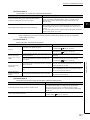
The following table shows signal names of the terminal block.
Input type
Pin
number
Terminal block
CH2
I+
CH2
V+/b
CH2
V-/B
CH2
A
CH4
I+
CH4
V+/b
CH4
V-/B
CH4
A
CH1
V+/b
Signal name
Current
Resistance
temperature
detector
Thermocouple
1
CH1
I+
Not used
I+
Not used
Not used
2
CH2
I+
Not used
I+
Not used
Not used
3
CH1
V+/b
V+
V+
+
b
4
CH2
V+/b
V+
V+
+
b
5
CH1
V-/B
V-
V-
CJ
B
6
CH2
V-/B
V-
V-
-
B
7
CH1
A
Not used
Not used
CJ
A
CH1
V-/B
8
CH2
A
Not used
Not used
Not used
A
CH1
A
9
CH3
I+
Not used
I+
Not used
Not used
CH3
I+
10
CH4
I+
Not used
I+
Not used
Not used
11
CH3
V+/b
V+
V+
+
b
12
CH4
V+/b
V+
V+
+
b
CH3
V+/b
CH3
V-/B
13
CH3
V-/B
V-
V-
-
B
CH3
A
14
CH4
V-/B
V-
V-
-
B
NC
15
CH3
A
Not used
Not used
Not used
A
16
CH4
A
Not used
Not used
Not used
A
17
NC
Not used
18
NC
Not used
6
6.2 Terminal Block
NC
CH1
I+
Voltage,
micro
voltage
37
(3) Removing and installing the terminal block
The following procedures show how to remove and install the terminal block.
(a) Removal procedure
1.
Open the terminal cover and loosen the terminal
block mounting screw.
Terminal block
mounting screw
2.
Use the terminal block fixing holes as a fulcrum and
remove the terminal block.
(b) Installation procedure
Terminal block fixing hole
1.
Fully insert the projections on the top of the
terminal block into the terminal block fixing holes
and press the terminal block until it snaps into
place.
2.
Open the terminal cover and tighten the terminal
block mounting screw.
Terminal block
mounting screw
38
CHAPTER 6 INSTALLATION AND WIRING
6.3
Wiring
The following figures show wiring to the terminal block.
(1) Voltage input, current input, and micro voltage input
For voltage input and micro voltage input
CH1
I+
CH2
I+
CH2
CH2
V+/b
CH2
V-/B
CH2
A
For current input
CH4
CH4
I+
CH4
V+/b
CH4
V-/B
CH4
A
CH1
V+/b
CH1
CH1
V-/B
CH1
A
CH3
I+
CH3
V+/b
6
CH3
CH3
V-/B
CH3
A
NC
6.3 Wiring
NC
39
(2) Thermocouple input
CH1
I+
CH2
I+
CH2
V+/b
CH2
CH2
V-/B
CH2
A
CH4
I+
CH4
V+/b
CH4
CH4
V-/B
CH4
A
CH1
V+/b
CH1
CH1
V-/B
CH1
A
CJ*1
CH3
I+
CH3
CH3
V+/b
CH3
V-/B
CH3
A
NC
NC
*1
To use the thermocouple input, always connect the cold junction compensation resistor (CJ) supplied with the module
between the CH1 V-/B terminal (pin number 5) and the CH1 A terminal (pin number 7).
(3) Resistance temperature detector input
CH1
I+
CH2
I+
CH2
CH2
V+/b
CH2
V-/B
CH2
A
CH4
I+
CH4
CH4
V+/b
CH4
V-/B
CH4
A
NC
40
CH1
V+/b
CH1
CH1
V-/B
CH1
A
CH3
I+
CH3
V+/b
CH3
V-/B
CH3
A
NC
CH3
CHAPTER 6 INSTALLATION AND WIRING
6.4
External Wiring
The following figures show the external wiring.
If the circuit between the terminals of unused channels is kept open and the conversion is enabled, an undefined digital
value may be output. To avoid this phenomenon, set CH Input type/range setting (Un\G500 to Un\G503) of the unused
channels to Conversion disable. Note that changing the value in CH Input type/range setting (Un\G500 to Un\G503) from
Conversion enable to Conversion disable reduces the conversion cycle.
(1) Voltage input, current input, and micro voltage input
⋅ For voltage input
Signal source -10 to 10V
*3
6
V+/b
I+
250Ω
1MΩ
A/D
conversion
1MΩ
A/D
conversion
V-/B
*1
*2
⋅ For current input
Signal source 0 to 20mA
*3
*4
V+/b
I+
250Ω
6.4 External Wiring
V-/B
*1
*2
⋅ For micro voltage input
Signal source -100 to 100mV
V+/b
Filter
A/D
conversion
V-/B
*1
*1
*2
*3
*4
*2
For the wire, use the 2-core shielded twisted pair cable.
Always ground the shield wire of the wire in each channel.
Indicates the input resistance of the multiple input module.
For the current input, always connect the (V+/b) terminal and (I+) terminal.
41
(2) Thermocouple input
V+/b
Temperature
conversion
Filter
V-/B
C
J
*1
*1
*2
*3
*2
A
*3
Always use the shielded compensation lead wire.
Always ground the shield wire of the compensation lead wire in each channel.
To use the thermocouple input, always connect the cold junction compensation resistor (CJ) supplied with the module
between the CH1 V-/B terminal (pin number 5) and the CH1 A terminal (pin number 7).
(3) Resistance temperature detector input
*4
*3
1)
A
V-/B
2)
Temperature
conversion
Filter
V+/b
*1
*1
*2
*3
*4
*2
*3
Always use a shielded cable.
Always ground the shield wire of the wire in each channel.
Adjust the conductor resistance values of 1) Conducting wire between the resistance temperature detector and A
terminal and 2) Conducting wire between the resistance temperature detector and V-/B terminal so that the difference
between the values is 10 or less. When the difference exceeds 10, the accuracy described on the following page
may not be satisfied (
Page 168, Appendix 4 (3)).
To connect a 2-wire resistance temperature detector, connect it between the A terminal and V-/B terminal and shortcircuit the V-/B terminal and V+/b terminal.
Note that the 2-wire connection is affected by a conductor resistance, and this can cause an error of the temperature
measured value. (Depending on the wiring condition, the conductor resistance value, the total of 1) + 2) in the following
figure, may become high.)
Conducting wire
1)
A
V-/B
2)
Conducting wire
42
V+/b
CHAPTER 7 VARIOUS SETTINGS
CHAPTER 7
VARIOUS SETTINGS
This chapter describes the setting procedures of the multiple input module.
After writing the settings of a new module, parameters, and auto refresh into the CPU module, reset the CPU module, switch
STOP RUN STOP RUN, or power off and on the module to validate the setting.
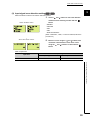
7.1
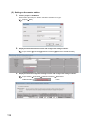
Adding a Module
Add the module name of a multiple input module to use on the project.
(1) Addition procedure
Open the "New Module" window.
Project window
[Intelligent Function Module]
Right-click
7
[New Module]
7.1 Adding a Module
Item
Module Selection
Mount Position
Title setting
Description
Module Type
Set "Multiple Input Module".
Module Name
Select the name of the module to be connected.
Mounted Slot No.
Set the slot No. where the module is connected.
Specify start XY address
The start I/O number (hexadecimal) of the module is set according to the mounted slot
No. Setting any start I/O number is also possible.
Title
Set any title.
43
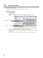
7.2
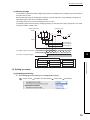
Parameter Settings
Set the parameters of each channel.
By setting the parameters, the setting by programming becomes unnecessary.
(1) Setting procedure
Open the "Parameter" window.
1.
Start "Parameter".
Project window
[Intelligent Function Module]
module name
[Parameter]
Select an item from the
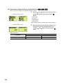
pull-down list.
Enter a value in the text box.
2.
Double-click the item to change the setting, and enter the setting value.
• Items to be selected from the pull-down list: Double-click the item to be set to display the pull-down list.
Select the item.
• Items to be entered in the text box: Double-click the item to be set and enter a numerical value.
44
CHAPTER 7 VARIOUS SETTINGS
3.
For setting CH2 to CH4, follow the operation of step 2.
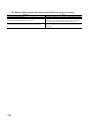
Item
Input type
Input range
Setting value
Current
0: 4 to 20mA (default value)
1: 0 to 20mA
2: 4 to 20mA (Extended Mode)
Voltage
0: 1 to 5V (default value)
1: 0 to 5V
2: -10 to 10V
3: 0 to 10V
4: 1 to 5V (Extended Mode)
0: -100 to 100mV (default value)
Resistance
Temperature
Detector
0: Pt100 (-20 to 120°C) (default value)
1: Pt100 (-200 to 850°C)
2: JPt100 (-20 to 120°C)
3: JPt100 (-200 to 600°C)
4: Pt1000 (-200 to 850°C)
5: Pt50 (-200 to 650°C)
Thermocouple
0: B Thermocouple (default value)
1: R Thermocouple
2: S Thermocouple
3: K Thermocouple
4: E Thermocouple
5: J Thermocouple
6: T Thermocouple
7: N Thermocouple
8: U thermocouple
9: L Thermocouple
10: PLII Thermocouple
11: W5Re/W26Re Thermocouple
Celsius/Fahrenheit display setting
0: Celsius [°C] (default value)
1: Fahrenheit [°F]
Averaging process setting
0: Sampling Processing (default value)
1: Time Average
2: Count Average
3: Moving Average
Input signal error
detection function
Disconnection
detection function
Scaling function
Input signal error detection setting
Time average
8 to 18000 (×100ms) (default value: 0)
Count average
4 to 36000 Times (default value: 0)
Moving average
2 to 1000 Times (default value: 0)
0: Disable (default value)
1: Upper and Lower Detection
2: Lower Detection
3: Upper Detection
4: Simple Disconnection Detection*1
Input signal error detection setting value
0 to 25.0% (default value: 5.0%)
Conversion setting for disconnection
detection
0: Value just before disconnection (default value)
1: Up Scale
2: Down scale
3: Optional value
Conversion setting value for disconnection
detection
-32768 to 32767 (default value: 0)
Scaling enable/disable setting
0: Enable
1: Disable (default value)
Scaling upper limit value
-32000 to 32000 (default value: 0)
Scaling lower limit value
-32000 to 32000 (default value: 0)
Page 50,
Section 8.2
7
Page 157,
Appendix 2
(22)
Page 53,
Section 8.3
Page 63,
Section 8.7
Page 59,
Section 8.6
Page 78,
Section 8.9
45
7.2 Parameter Settings
Minute Voltage
Basic setting
Time Average/Count Average/Moving
Average
Reference
0: Disable Conversion (default value)
1: Current
2: Voltage
3: Minute voltage
4: Resistance Temperature Detector
5: Thermocouple
Item
Warning output
function
*1
Setting value
Process alarm output setting
0: Enable
1: Disable (default value)
Process alarm upper upper limit value
-32768 to 32767 (default value: 0)
Process alarm upper lower limit value
-32768 to 32767 (default value: 0)
Process alarm lower upper limit value
-32768 to 32767 (default value: 0)
Process alarm lower lower limit value
-32768 to 32767 (default value: 0)
Rate alarm output setting
0: Enable
1: Disable (default value)
Rate alarm detection cycle
1 to 36000 Times (default value: 0)
Rate alarm upper limit value
-3276.8 to 3276.7% (default value: 0)
Rate alarm lower limit value
-3276.8 to 3276.7% (default value: 0)
Reference
Page 70,
Section 8.8 (1)
Page 72,
Section 8.8 (2)
This item can be set only when "2: 4 to 20mA (Extended Mode)" or "4: 1 to 5V (Extended Mode)" is selected for "Input
range".
● Changing "Input type" automatically changes "Input range" to its default value.
● For "Conversion setting value for disconnection detection", "Process alarm upper upper limit value", "Process alarm
upper lower limit value", "Process alarm lower upper limit value", and "Process alarm lower lower limit value", the setting
method differs depending on each input type/input range.
Changing "Input type", "Input range", "Celsius/Fahrenheit display setting", or "Scaling enable/disable setting" after the
setting of the above items automatically changes the location of the decimal point or unit.
Input type/input range
46
Setting procedure
• Resistance temperature detector: Pt100 (-20 to 120°C)
• Resistance temperature detector: JPt100 (-20 to 120°C)
Set the temperature in increments of 0.01°C (or 0.01°F).
• Resistance temperature detector input range other than the above
• Thermocouple input range
Set the temperature in increments of 0.1°C (or 0.1°F).
CHAPTER 7 VARIOUS SETTINGS
7.3
Auto Refresh
Set the buffer memory of the multiple input module to be refreshed automatically.
By the auto refresh setting, reading data using a program becomes unnecessary.
(1) Setting procedure
Open the "Auto_Refresh" window.
1.
Start "Auto_Refresh".
Project window
2.
[Intelligent Function Module]
module name
[Auto_Refresh]
Click the item to be set, and enter the auto refresh target device.
7
7.3 Auto Refresh
Available devices are X, Y, M, L, B, T, C, ST, D, W, R, and ZR.
When a bit device X, Y, M, L, or B is used, set the number that is divisible by 16 points (example: X10, Y120, M16). Data in
the buffer memory are stored in 16 points of devices from the set device No. (Example: If X10 is set, the data are stored in
X10 to X1F.)
47
CHAPTER 8
FUNCTIONS
This chapter describes the functions of the multiple input module and the setting procedures for those functions.
For details on the I/O signals and the buffer memory, refer to the following.
• Details of I/O Signals (
Page 134, Appendix 1)
• Details of Buffer Memory Addresses (
48
Page 140, Appendix 2)
CHAPTER 8 FUNCTIONS
8.1
Processing Order of Each Function
Analog input values and the digital values of the following (1) to (3) are processed in the order shown below. If multiple
functions are enabled, the output of the first processed function is used as the input of the next function.
Analog input
(CH1 to CH4)
Input signal
error detection
function or
disconnection
detection
function
CH Digital output
value (Un\G11 to
Un\G14)
Averaging
processing
CH Maximum value
(Un\G30, Un\G32,
Un\G34, Un\G36)
Warning output
function
⋅ Process alarm
⋅ Rate alarm
CH Minimum value
(Un\G31, Un\G33,
Un\G35, Un\G37)
Scaling
function
CH Scaling value
(Un\G54 to Un\G57)
(1) Digital output value
The digital values obtained in sampling processing or averaging processing are stored.
8
(2) Scaling value
The values obtained in scale conversion of digital output values by the scaling function are stored. When the
(3) Maximum and minimum values
The maximum digital output value and minimum digital output value are stored. When the scaling function is
used, the maximum scaling value and minimum scaling value are stored.
● When averaging processing (time average/count average) is performed on digital output values, scaling values, and
maximum and minimum values, the values are stored at every averaging process cycle.
● For the micro voltage input range, resistance temperature detector input range, or thermocouple input range, the
conversion is stopped when a disconnection is detected.
The digital values in this case are as follows:
• Digital output value: The values are stored according to the setting in Conversion setting at disconnection
detection (Un\G400).
• Scaling value: The values obtained in scale conversion of digital output values by the scaling function are stored.
• Maximum value/Minimum value: The values are updated based on the settings in Conversion setting at
disconnection detection (Un\G400).
The conversion restarts when the disconnected wiring is reconnected.
For details on the disconnection detection function, refer to the following.
• Disconnection Detection Function (
Page 59, Section 8.6)
● In the use of the input signal error detection function, conversion is stopped if an input signal error is detected.
In this case, the digital output values, scaling values, and maximum and minimum values are not updated. The values
obtained before the input signal error is detected are held.
When the analog input signal returns to a normal value, conversion resumes.
For details on the input signal error detection function, refer to the following.
• Input Signal Error Detection Function (
Page 63, Section 8.7)
49
8.1 Processing Order of Each Function
scaling function is not used, the values same as the digital output values are stored.
8.2
Input Type/Range Setting
The input type and input range that are to be used can be selected for each channel.
(1) Setting procedure
Set "Input type" and "Input range" depending on the sensor type to be connected.
1.
Set "Input type".
Project window
2.
[Intelligent Function Module]
module name
[Parameter]
Set "Input range".
Input type
0: Disable Conversion (default
value)
1: Current
Input range
3: Minute voltage
4: Resistance Temperature
Detector
Input range
-
0: B Thermocouple
0: 4 to 20mA
1: R Thermocouple
1: 0 to 20mA
2: S Thermocouple
2: 4 to 20mA (Extended Mode)
3: K Thermocouple
0: 1 to 5V
4: E Thermocouple
1: 0 to 5V
2: Voltage
Input type
5: Thermocouple
5: J Thermocouple
2: -10 to 10V
6: T thermocouple
3: 0 to 10V
7: N Thermocouple
4: 1 to 5V (Extended Mode)
8: U Thermocouple
0: -100 to 100mV
9: L Thermocouple
0: Pt100 (-20 to 120°C)
10: PLII Thermocouple
1: Pt100 (-200 to 850°C)
11: W5Re/W26Re Thermocouple
2: JPt100 (-20 to 120°C)
3: JPt100 (-200 to 600°C)
4: Pt1000 (-200 to 850°C)
5: Pt50 (-200 to 650°C)
The default setting is "Disable Conversion". Change the setting depending on the sensor type to be connected.
50
CHAPTER 8 FUNCTIONS
(2) Precautions for the thermocouple input
(a) Input type
When the thermocouple input is used, the thermocouple input range must be set for CH1. If the input type of
CH1 is set to a type other than the thermocouple input range and the input type of any of CH2 to CH4 is set to
the thermocouple input range, an error (error code: 15) occurs in the channel where the thermocouple input
range is set and the conversion is not performed.
The following table lists setting examples.
Input type/Input range
Setting example
CH1
When only one channel is
used for the thermocouple
input
When three channels are
used for the thermocouple
input (An input type other
than the thermocouple
input is used for the one
channel left.)
When three channels are
used for the thermocouple
input (A setting error
occurs.)
5: Thermocouple
0: B Thermocouple
5: Thermocouple
0: B Thermocouple
2: Voltage
3: 0 to 10V
CH2
1: Current
0: 4 to 20mA
2: Voltage
3: 0 to 10V
5: Thermocouple
0: B Thermocouple
CH3
2: Voltage
3: 0 to 10V
5: Thermocouple
1: R Thermocouple
5: Thermocouple
1: R Thermocouple
Result
CH4
4: Resistance
Temperature
Detector
0: Pt100 (-20 to
120°C)
Since the thermocouple input is
used only for CH1, the conversion
is performed with no errors.
5: Thermocouple
2: S Thermocouple
Since the thermocouple input is
used for CH1, the conversion is
performed with no errors.
Two channels of CH2 to CH4 are
available for the thermocouple
input.
5: Thermocouple
2: S Thermocouple
Since an input type other than the
thermocouple input is used for
CH1, an error (error code: 152,
153, 154) occurs and the
conversion is not performed.
×
8
(b) Cold junction compensation resistor (CJ)
Connect the cold junction compensation resistor (CJ) supplied with the module between the CH1 V-/B terminal
When the cold junction compensation resistor (CJ) is not connected, all the channels for the thermocouple
input are in the disconnection detection state.
For details on the disconnection detection function, refer to the following.
Page 59, Section 8.6
(3) Enabling conversion and disabling conversion
Whether to enable or disable the conversion for each channel can be set in "Input type" and "Input range". In this
manual, the enabled conversion and disabled conversion are defined as follows.
(a) Conversion disabled
The state generated by selecting "0: Disable Conversion" in "Input type". In this case, the conversion is not
performed in the target channel.
"0: Disable Conversion" is set to all the channels in the multiple input module by default. Thus, change the
setting values of "Input type" and "Input range" depending on the connected sensor type.
(b) Conversion enabled
The state generated by selecting values for "Input type" and "Input range" based on the connected sensor type
(values other than "0: Disable Conversion" for "Input type"). In this case, the conversion is performed in the
target channel.
51
8.2 Input Type/Range Setting
(pin number 5) and the CH1 A terminal (pin number 7).
(4) Conversion cycle
The conversion cycle varies depending on the number of channels where the conversion is enabled.
For details, refer to the following.
Page 53, Section 8.3 (1)
(5) When the value in CH Input type/range setting (Un\G500 to Un\G503) is
changed during module operations
The stored values in the following buffer memory areas are cleared to 0.
When the first conversion in the changed input type/range is finished, the first conversion value is stored in the
following buffer memory areas. However, when CH Input type/range setting (Un\G500 to Un\G503) is set to
Disable conversion (0000H) or set to a value out of the setting range, the conversion is stopped and the stored
values in the following buffer memory remain 0.
• CH Digital output value (Un\G11 to Un\G14)
• CH Maximum value (Un\G30, Un\G32, Un\G34, Un\G36)
• CH Minimum value (Un\G31, Un\G33, Un\G35, Un\G37)
• CH Scaling value (Un\G54 to Un\G57)
52
CHAPTER 8 FUNCTIONS
8.3
Conversion Method
Set sampling processing or averaging processing for each channel.
(1) Sampling processing
Analog input values and temperature input values are converted at every sampling cycle and stored in the buffer
memory as digital output values.
The conversion cycle is "Conversion cycle (50ms) × Number of channels where conversion is enabled".
Whether to enable or disable can be set for each channel. Disabling the conversion for unused channels reduces the
conversion cycles.
For example, when the conversion is enabled in two channels (CH1, CH2), the conversion cycle is 100ms (50ms × 2).
(2) Averaging processing
Averaging processing is performed on digital output values for each channel. The values obtained in averaging
processing are stored in the buffer memory area.
The following three types of averaging processing are provided.
• Time average
• Count average
8
• Moving average
(a) Time average
The conversion is performed for a set period of time and averaging processing is performed on the total value
the buffer memory area.
The number of processing times within a set period of time changes depending on the number of channels
where the conversion is enabled.
The setting range of the time (for averaging) is from 8 to 18000 (set in increments of 100ms; 800ms to
1800000ms).
Setting time (value) × 100ms
Number of
=
processing (times)
50ms × Number of channels where conversion is enabled
Processing count with the following settings
Item
Setting
Number of channels where conversion is enabled
2 channels (CH1, CH2)
Set period of time
22 (2200ms)
2200
50 × 2
= 22 (times) ⋅⋅⋅ Numbers after the decimal point are rounded down.
→ The processing is performed 22 times and its average value is output.
53
8.3 Conversion Method
excluding the maximum and the minimum values. The values obtained in averaging processing are stored in
(b) Count average
The conversion is performed a set number of times and averaging processing is performed on the total value
excluding the maximum and the minimum values. The values obtained in averaging processing are stored in
the buffer memory area.
The time taken to store the average value, obtained by the average processing, into the buffer memory area
changes depending on the number of channels where the conversion is enabled.
The setting range of the count (for averaging) is from 4 to 36000.
Processing time (ms) = Number of settings × (50ms × Number of channels where conversion is enabled)
Processing time with the following settings
Item
Setting
Number of channels where conversion is enabled
2 channels (CH1, CH2)
Set number of times
20 times
20 × (50 × 2) = 2000 (ms) An average value is output every 2000ms.
Because the count average requires a sum of at least two counts excluding the maximum and minimum values, set four or
larger number of counts.
54
CHAPTER 8 FUNCTIONS
(c) Moving average
The average of a specified number of digital output values is calculated at every sampling cycle and is stored in
the buffer memory area.
Because the target range for averaging processing is moved in response to every sampling processing, the
latest digital output value can be constantly obtained.
The setting range of the count (for averaging) is from 2 to 1000.
The following figure shows the moving average processing of when the current input range is set to 4 to 20mA
and the set number of times is four.
Sampling cycle
Digital output value
20000
2)
3)
4)
5)
1)
6)
7)
8)
9)
12)
10) 11)
10000
1st storage (a)
2nd storage (b)
3rd storage (c)
0
CH1 Digital output value (Un\G11)
Time [ms]
0
(a)
(b)
(c)
ON
8
Conversion completed flag (XE)
Data transition in buffer memory
2nd storage (b)
3rd storage (c)
2) + 3) + 4) + 5)
3) + 4) + 5) + 6)
4
4
4
8.3 Conversion Method
1st storage (a)
1) + 2) + 3) + 4)
(3) Setting procedure
(a) Sampling processing
1.
Set "Averaging process setting" to "0: Sampling Processing".
Project window
[Intelligent Function Module]
module name
[Parameter]
55
(b) Averaging processing
Ex. When "1: Time Average" is set to "Averaging process setting"
1.
Set "Averaging process setting" to "1: Time Average".
Project window
2.
[Intelligent Function Module]
module name
Set an averaging processing value for "Time Average/Count Average/Moving Average".
Setting item
56
[Parameter]
Setting range
Time Average
8 to 18000 (800ms to 1800000ms)
Count Average
4 to 36000 times
Moving Average
2 to 1000 times
CHAPTER 8 FUNCTIONS
8.4
Current
Input Range Extension Function
Voltage
This function extends and converts the input range of 4 to 20mA and that of 1 to 5V.
Input range
setting
Input range
4 to 20mA
4 to 20mA
Digital output value
Input range
setting
Input range
4 to 20mA
(Extended mode)
0.0 to 22.0mA
1 to 5V
(Extended mode)
0.0 to 5.5V
0 to 20000
1 to 5V
1 to 5V
Digital output value
-5000 to 22500
(1) Overview
• Although the slope of the I/O characteristic of the extended mode is the same as that of the normal range,
the upper limit value and the lower limit value of the input range and the digital output value are extended.
For details, refer to I/O Conversion Characteristic of Current/Voltage (
Page 161, Appendix 3).
• The resolution is the same as that the input range of 4 to 20mA and 1 to 5V has (800nA and 200µV).
Therefore, the conversion with higher resolution than that of the input range of 0 to 20mA and 0 to 5V
(resolution of 1000nA and 250µV) is achieved.
8
(2) Setting procedure
1.
Set "1: Current" or "2: Voltage" for "Input type".
2.
[Intelligent Function Module]
module name
[Parameter]
8.4 Input Range Extension Function
Project window
Set the range of the extended mode for "Input range".
When the input range extension function is used simultaneously with the scaling function, the scaling values may exceed the
range of -32768 to 32767.
In that case, the upper limit value (32767) or the lower limit value (-32768) is stored as a scaling value.
Ex. When 32000 is set for the scaling upper limit value and -32000 is set for the scaling lower limit value, the following
operations are performed.
• When the digital output value is 20240 or greater, 32767 is stored as a scaling value.
• When the digital output value is -240 or smaller, -32768 is stored as a scaling value.
57
8.5
Maximum Value/Minimum Value Hold Function
This function stores the maximum digital value and minimum digital output value in the buffer memory area for each
channel.
Values are updated at every averaging process cycle if averaging processing is selected, otherwise updated at every
sampling cycle.
For the buffer memory address where the values are stored, refer to the following.
• List of Buffer Memory Addresses (
Page 27, Section 3.5)
(1) Resetting the maximum value and the minimum value
When one of the following operations is performed, the maximum value and the minimum value are replaced with
the current digital output value.
• Turning on and off Maximum value/minimum value reset request (YD)
• Turning on and off Operating condition setting request (Y9)
When the input type/range setting is changed and Operating condition setting request (Y9) is turned on and off,
the maximum value and the minimum value are cleared to 0.
(2) Target value for the maximum value/minimum value hold function
The maximum digital output value and minimum digital output value are stored.
If the scaling function is enabled, the maximum scaling value and minimum scaling value are stored.
58
CHAPTER 8 FUNCTIONS
8.6
Micro voltage
Disconnection Detection Function
Thermocouple
RTD
This function detects a disconnection of the external wiring (resistance temperature detector, conducting wire,
thermocouple, cold junction compensation resistor (CJ), or compensation lead wire) when the input type is micro
voltage, resistance temperature detector, or thermocouple.
(1) Notifying disconnections
• Disconnection (1) is stored in the bit of Disconnection detection flag (Un\G47) corresponding to the channel
number.
• Disconnection detection signal (X6) turns on.
• The ALM LED flashes.
• The alarm code (130) is stored in Latest error code (Un\G19).
• One of "Value just before disconnection", "Up scale", "Down scale", or "Optional value" specified in
Conversion setting at disconnection detection (Un\G400) is stored in CH Digital output value (Un\G11 to
Un\G14).
(2) Relation between disconnection detection and conversion enable/disable
setting
8
Disconnection detection is executed only in the channel where the conversion is enabled.
The following table shows the relation between the disconnection detection and conversion enable/disable
setting. (The conversion enable/disable setting can be performed in CH Input type/range setting (Un\G500 to
Un\G503).)
Status of the conversion enable/disable setting
A
Disconnection detection flag
Conversion enabled
B
b
8.6 Disconnection Detection Function
Connection status
Off
Conversion disabled
No disconnection
A
Conversion enabled
On
Conversion disabled
Off
Conversion enabled
On
Conversion disabled
Off
B
b
Disconnection
A
B
b
No connection
59
● When a disconnection and warning output (process alarm or rate alarm) occur simultaneously, the ALM LED flashes.
For details on the warning output function, refer to the following.
• Warning Output Function (
Page 70, Section 8.8)
● For Disconnection detection flag (Un\G47), Disconnection detection signal (X6), the ALM LED, and Latest error code, the
status at a disconnection detection is held even after the disconnected wiring is reconnected. Turn on and off Error clear
request (YF) to clear the error.
● To use the thermocouple input, always connect the cold junction compensation resistor (CJ) supplied with the module
between the CH1 V-/B terminal (pin number 5) and the CH1 A terminal (pin number 7). When the cold junction
compensation resistor (CJ) is not connected, the disconnection is detected in all the channels for which the thermocouple
input range is set.
When a disconnection of the cold junction compensation resistor (CJ) is detected, a disconnection is also detected in all
the channels for which the thermocouple input range is set.
(3) Conversion setting at disconnection detection
Setting Conversion setting at disconnection detection (Un\G400) allows specifying the value to be stored in CH
Digital output value (Un\G11 to Un\G14). Thus, the disconnection detection is enabled only by checking CH
Digital output value (Un\G11 to Un\G14) without monitoring Disconnection detection signal (X6).
By default, Value just before disconnection (0) is set in Conversion setting at disconnection detection (Un\G400).
Change the setting value as needed.
Conversion setting at
disconnection
detection
Processing in disconnection detection
Value just before
disconnection (0)
The value immediately before a disconnection detection is held in CH Digital output value (Un\G11 to Un\G14).
Up Scale (1)
The up-scale value (upper limit value + 5% of the input range) of the input range currently set is stored in CH Digital output value
(Un\G11 to Un\G14).
Down Scale (2)
The down-scale value (lower limit value - 5% of the input range) of the input range currently set is stored in CH Digital output
value (Un\G11 to Un\G14).
Optional Value (3)
The value set in CH Conversion setting value at disconnection detection (Un\G404 to Un\G407) is stored in CH Digital output
value (Un\G11 to Un\G14).
With the scaling function enabled, a value obtained by performing the scale conversion on the set value in Conversion
setting at disconnection detection (Un\G400) is stored in CH Scaling value (Un\G54 to Un\G57) when a disconnection is
detected.
60
CHAPTER 8 FUNCTIONS
(a) Up scale and down scale
The up-scale value (upper limit value + 5% of the input range) and down-scale value (lower limit value - 5% of
the input range) of the input range currently set is stored in CH Digital output value (Un\G11 to Un\G14) when
a disconnection is detected.
If the value of "upper limit value + 5% of the input range" exceeds 32767 when the up scale is selected, 32767
is stored in CH Digital output value (Un\G11 to Un\G14).
If the up scale or down scale is selected, the following values are stored in CH Digital output value (Un\G11 to
Un\G14) when a disconnection is detected.
• Micro voltage
Input range
-100 to 100mV
Output range of digital output value
Up scale
-20000 to 20000
22000
Down scale
-22000
• Resistance temperature detector
Celsius
Input range
Output range of
digital output value
Up scale
Fahrenheit
Down scale
Output range of
digital output value
Up scale
Down scale
Pt100 (-20 to 120°C)
-2000 to 12000
12700
-2700
0 to 20000
21000
Pt100 (-200 to 850°C)
-2000 to 8500
9025
-2525
-3000 to 15000
15900
-1000
-3900
JPt100 (-20 to 120°C)
-2000 to 12000
12700
-2700
0 to 20000
21000
-1000
JPt100 (-200 to 600°C)
-2000 to 6000
6400
-2400
-3000 to 11000
11700
-3700
Pt1000 (-200 to 850°C)
-2000 to 8500
9025
-2525
-3000 to 15000
15900
-3900
Pt50 (-200 to 650°C)
-2000 to 6500
6925
-2425
-3000 to 12000
12750
-3750
8
• Thermocouple
Celsius
Input range
Output range of
digital output value
Up scale
Fahrenheit
Down scale
Output range of
digital output value
Up scale
Down scale
-1264
*1
-1600
0 to 32000
32767*1
-1600
-3520
-4000 to 24000
25400
-5400
-3335
-4000 to 18000
19100
-5100
-4200
0 to 18200
19110
-910
320 to 32000
Type R thermocouple
-500 to 17600
18505
-1405
0 to 32000
32767
Type S thermocouple
-500 to 17600
18505
-1405
Type K thermocouple
-2700 to 13700
14520
Type E thermocouple
-2700 to 10000
10635
Type J thermocouple
-2100 to 12000
12705
-2805
-3000 to 21000
22200
Type T thermocouple
-2700 to 4000
4335
-3035
-3000 to 6000
6450
-3450
Type N thermocouple
-2700 to 13000
13785
-3485
-4000 to 23000
24350
-5350
Type U thermocouple
-2000 to 6000
6400
-2400
-3000 to 11000
11700
-3700
Type L thermocouple
-2000 to 9000
9550
-2550
-3000 to 16000
16950
-3950
Type PL II thermocouple
0 to 13900
14595
-695
320 to 25000
26234
-914
Type W5Re/W26Re
thermocouple
0 to 23000
24150
-1150
320 to 32000
32767*1
-1264
*1
8.6 Disconnection Detection Function
32767*1
Type B thermocouple
Because the up-scale value exceeds 32767, 32767 is stored.
(b) Optional value
The value set in CH Conversion setting value at disconnection detection (Un\G404 to Un\G407) is stored in
CH Digital output value (Un\G11 to Un\G14) when a disconnection is detected.
The default value of CH Conversion setting value at disconnection detection (Un\G404 to Un\G407) is 0. The
disconnection detection function is available with 0. However, the value can be changed to any value.
61
(4) When the disconnected wiring is reconnected
A normal digital output value is stored in the buffer memory area in the next conversion after recovery from the
disconnection. When the averaging processing has been performed, the normal digital output value is stored in
the buffer memory after the disconnected wiring is reconnected and the averaging process cycle elapses.
Until the normal digital output value is stored in the buffer memory area, the digital output value remains a
specified value in the conversion setting at disconnection detection (such as the down-scale value).
(5) Setting procedure
1.
In "Conversion setting for disconnection detection", set a value to be stored in CH Digital output
value (Un\G11 to Un\G14) at disconnection detection.
Project window
2.
[Intelligent Function Module]
module name
When "3: Optional Value" is set, set "Conversion setting value for disconnection detection".
Item
Conversion setting value for disconnection detection
62
[Parameter]
Setting range
-32768 to 32767
CHAPTER 8 FUNCTIONS
8.7
Current
Input Signal Error Detection Function
Voltage
This function outputs an alarm if an analog input value exceeds a preset range, provided that the input type is voltage
or current.
Within the detection range
Out of the detection range
Included
Analog
input value
Input signal error
detection upper
limit value
CH1 Analog input
value
Normal input value
Input signal error
detection lower
limit value
Error
detected
Time
ON
8
OFF
CH1 Input signal error detection flag
(Un\G49.b0)
ON
Input signal error detection signal (XC)
8.7 Input Signal Error Detection Function
OFF
CH1 Conversion completed flag (Un\G10.b0)*1
ON
Error clear request (YF)
OFF
*1 This flag does not turn off if a input signal error is detected.
63
(1) Detection method
One of the following detection methods can be selected.
Detection method
(Set value of Input
signal error
detection setting
(Un\G402))
Disable (0)
Detection condition
Input signal error detection is not performed.
Analog
input value
When the analog input value becomes equal to or greater than
the input signal error detection upper limit value, or becomes
equal to or smaller than the input signal error detection lower limit
value, an error is detected.
Upper and Lower
Detection (1)
Input signal error
detection upper
limit value
Input signal error
detection lower
limit value
Error
detection
Error
detection
Time
Analog
input value
Lower Detection (2)
When the analog input value becomes equal to or smaller than
the input signal error detection lower limit value, an error is
detected. If the analog input value becomes equal to or greater
than the input signal error detection upper limit value, an error is
not detected.
Input signal error
detection upper
limit value
Input signal error
detection lower
limit value
No error
detection
Error
detection
Time
Analog
input value
Upper Detection (3)
When the analog input value becomes equal to or greater than
the input signal error detection upper limit value, an error is
detected. If the analog input value becomes equal to or smaller
than the input signal error detection lower limit value, an error is
not detected.
Input signal error
detection upper
limit value
Input signal error
detection lower
limit value
Error
detection
No error
detection
Time
Simple
Disconnection
Detection (4)
Simple disconnection detection is performed. For details, refer to the following.
• Simple disconnection detection (
Page 65, Section 8.7 (1) (a))
When an input signal error and warning output (process alarm or rate alarm) occur simultaneously, the ALM LED flashes.
For details on the warning output function, refer to the following.
• Warning Output Function (
64
Page 70, Section 8.8)
CHAPTER 8 FUNCTIONS
(a) Simple disconnection detection
Combining with the input range extension function allows a simple disconnection detection. If either of the
following conditions is satisfied, Input signal error (1) is stored in the bit of Input signal error detection flag
(Un\G49) corresponding to the channel number.
Input range
Disconnection detection condition
4 to 20mA (extended mode)
Analog input value 2mA
1 to 5V (extended mode)
Analog input value 0.5V
Analog
input value
2mA or 0.5V
Error
detection
Time
The setting in CH Input signal error detection setting value (Un\G412 to Un\G415) is ignored.
(2) Notifying input signal errors
If an input signal error or a disconnection is detected, the error is notified by Input signal error detection flag
(Un\G49), Input signal error detection signal (XC), and the flashing ALM LED. In addition, the alarm code (11
)
8
is stored in Latest error code (Un\G19). The stored value of an alarm code differs depending on the value of the
detected input signal error (upper detection, lower detection, or simple disconnection detection).
11
Fixed
8.7 Input Signal Error Detection Function
The following figure shows the alarm codes stored.
The last digit indicates the channel where an input signal error has occurred.
The second to the last digit indicates the state of the set value as one of the following:
1: Upper detection
2: Lower detection
3: Simple disconnection detection
For details of the alarm codes, refer to the following.
• List of Alarm Codes (
Page 127, Section 11.5)
65
(3) Operations performed when an input signal error is detected
On the channel where an error is detected, the digital output value obtained immediately before the error is
detected is held. At this time, Conversion completed flag (Un\G10) does not turn off.
If the analog input value falls back within the set range, conversion resumes regardless of whether or not Input
signal error detection flag (Un\G49) and Input signal error detection signal (XC) are reset. (The ALM LED keeps
flashing.)
During an input signal error, the values of CH Digital output value (Un\G11 to Un\G14) and CH Scaling value (Un\G54 to
Un\G57) are not updated.
(4) Detection cycle
The detection of an input signal error is performed at every sampling cycle.
(5) Clearing input signal errors
After the analog input value returns within the set range, turn on and off Error clear request (YF). If the simple
disconnection detection is set, turn on and off Error clear request (YF) after the analog input value exceeds
2.0mA or 0.5V.
When an input signal error is cleared, the multiple input module performs as follows.
• Clears Input signal error detection flag (Un\G49).
• Turns off Input signal error detection signal (XC).
• Turns off the ALM LED.
• Clears the alarm code (11
66
) stored in Latest error code (Un\G19).
CHAPTER 8 FUNCTIONS
(6) How to set the input signal error detection setting value
Set the input signal error detection upper limit value and input signal error detection lower limit value by 1 (0.1%)
based on the input signal error detection setting value.
Both the input signal error detection upper limit value and the input signal error detection lower limit value reflect
the input signal error detection setting value.
(a) Input signal error detection upper limit value
This value is calculated by adding "Input range width (gain value - offset value) × Input signal error detection
setting value" to the gain value. Only the value equal to or greater than the gain value can be set.
To calculate the input signal error detection setting value based on the input signal error detection upper limit
value, use the following equation:
Input signal error detection
setting value
=
Input signal error detection
upper limit value
-
Gain value of each range
Gain value of each range
-
Offset value of each range
1000
(b) Input signal error detection lower limit value
This value is calculated by subtracting "Input range width (gain value - offset value) × Input signal error
detection setting value" from the lower limit value of each range. Only the value below the lower limit value of
the range can be set.
To calculate the input signal error detection setting value based on the input signal error detection lower limit
value, use the following equation:
Input signal error detection
setting value
=
Lower limit value of each
range
Gain value of each range
-
IInput signal error detection
lower limit value
Offset value of each range
8
1000
8.7 Input Signal Error Detection Function
Remark
The following table lists the lower limit value, offset value, and gain value for each range.
Input range
Current
Voltage
Lower limit value
Offset value
Gain value
4 to 20mA
4mA
20mA
0 to 20mA
0mA
20mA
4 to 20mA (extended mode)
4mA
20mA
1 to 5V
1V
5V
0 to 5V
0V
5V
-10 to 10V
-10V
0V
10V
0 to 10V
0V
10V
1 to 5V (extended mode)
1V
5V
67
(7) Setting procedure
1.
Select a detection method from "Input signal error detection setting".
Project window
2.
[Intelligent Function Module]
module name
[Parameter]
Set a value for "Input signal error detection setting value".
Item
Input signal error detection setting value
Setting range
0 to 25.0%
● When "4: Simple Disconnection Detection" is set for "Input signal error detection setting", the setting for "Input signal
error detection setting value" becomes invalid.
● When the input type is set to voltage or current for CH Input type/range setting (Un\G500 to Un\G503) and when "4:
Simple Disconnection Detection" is set for "Input signal error detection setting" on the channel where the input range is
set to a range other than 4 to 20mA (extended mode) and 1 to 5V (extended mode), an error occurs. The error code
(82) is stored in Latest error code (Un\G19) and Error flag (XF) turns on.
● When the specifications of simple disconnection detection, 2mA (4 to 20mA (extended mode) or 0.5V (input range: 1 to
5V (extended mode)), do not fill the needs of the system, set "Input signal error detection setting" to "2: Lower Detection"
and set "Input signal error detection setting value" to a judging value to detect a disconnection.
68
CHAPTER 8 FUNCTIONS
(8) Setting example of input signal error detection
To detect an error on a channel where CH Input type/range setting (Un\G500 to Un\G503) is set to the current
of 4 to 20mA when the analog input value is 2.4mA or lower, make the following substitutions in the equation
based on the input signal error detection lower limit value.
• Input signal error detection lower limit value: 2.4mA
• Lower limit value of the input range (offset value): 4.0mA
• Gain value: 20.0mA
Input signal error detection =
setting value
=
4.0 - 2.4
1000
20.0 - 4.0
100(10.0%)
Thus, set the input signal error detection setting value to "100(10.0%)".
When "2: Lower Detection" is set for "Input signal error detection setting", the input signal error detection
value works as shown below.
Error
detection
Input signal error detection
upper limit value
21.6mA
1.6mA
(10.0% of 16mA)
Gain value
8
20mA
16mA
(Gain value - Offset value)
8.7 Input Signal Error Detection Function
Input range
lower limit value
(Offset value)
4mA
1.6mA
(10.0% of 16mA)
2.4mA
Input signal error detection
lower limit value
Error
detection
69
8.8
Warning Output Function
(1) Process alarm
When a digital output value falls within a preset warning output range, a warning is output.
When the scaling function is enabled, the scaling value is the warning detection target.
Alert output range
Out of alert output range
Digital output value
Included
Alert
Alert
Upper upper
limit value
Upper lower
limit value
Alert cleared
Alert cleared
CH1 digital output value
Alert cleared
Lower upper
limit value
CH2 digital output value
Lower lower
limit value
Alert
Time
ON
CH1 Warning output flag
(Process alarm upper limit value)
(Un\G50.b0)
OFF
CH1 Warning output flag
(Process alarm lower limit value)
(Un\G50.b1)
OFF
CH2 Warning output flag
(Process alarm upper limit value)
(Un\G50.b2)
OFF
Warning output signal (X8)
OFF
OFF
ON
OFF
ON
OFF
ON
OFF
(a) Operation performed when a warning is output
When the digital output value falls within a warning output range, equal to or larger than the process alarm
upper upper limit value or equal to or less than the process alarm lower lower limit value, a warning is notified
by the following operations.
• Alarm ON (1) is stored in the bit of Warning output flag (process alarm) (Un\G50) corresponding to the
channel number (upper limit alarm or lower limit alarm).
• Warning output signal (X8) turns on.
• The ALM LED turns on.
• The alarm code (10
) is stored in Latest error code (Un\G19). The following figure shows the alarm
codes stored.
10
Fixed
Process alarm channel number
0: Process alarm upper limit
1: Process alarm lower limit
The conversion in the channels where a warning is output continues.
70
CHAPTER 8 FUNCTIONS
(b) Operation performed after a warning is output
When the digital output value is smaller than the process alarm upper lower limit value or larger than the rate
alarm lower upper limit value after a warning is output, Normal (0) is stored in the bit of Warning output flag
(process alarm) (Un\G50) in the corresponding channel.
When the values in all the channels fall within the setting range, Warning output signal (X8) and the ALM LED
turn off.
However, the alarm code (10
) stored in Latest error code (Un\G19) is not cleared. Turn on and off Error
clear request (YF) to clear the alarm code (10
).
(c) Warning detection period
When the time average is specified, the warning detection is performed per set time (for averaging). When the
count average is specified, it is performed per count (for averaging).
When another conversion method is specified, it is performed per sampling cycle.
(d) Warning detection target
When the scaling function is enabled, the value in CH Scaling value (Un\G54 to Un\G57) is the warning
detection target.
For the setting of CH1 Process alarm lower lower limit value (Un\G86) to CH4 Process alarm upper upper limit
value (Un\G101), set values in consideration of the scale conversion.
(e) Operation performed when a disconnection is detected
For the micro voltage input range, resistance temperature detector input range, or thermocouple input range, a
process alarm may occur simultaneously because the value in CH Digital output value (Un\G11 to Un\G14)
changes depending on the value in Conversion setting at disconnection detection (Un\G400) when a
8
disconnection is detected.
1.
Set "Process alarm output setting" to "0: Enable".
Project window
2.
[Intelligent Function Module]
module name
[Parameter]
Set values for "Process alarm upper upper limit", "Process alarm upper lower limit", "Process
alarm lower upper limit", and "Process alarm lower lower limit".
Item
Setting range
Process alarm upper upper limit value
Process alarm upper lower limit value
Process alarm lower upper limit value
-32768 to 32767
Process alarm lower lower limit value
Set the warning output setting in the following condition.
Process alarm upper upper limit value Process alarm upper lower limit value Process alarm lower upper limit value
Process alarm lower lower limit value
71
8.8 Warning Output Function
(f) Setting procedure
(2) Rate alarm
When the change rate of a digital output value is equal to or larger than the rate alarm upper limit value or equal
to or smaller than the rate alarm lower limit value, a warning is output.
Digital output
value
Change rate of
digital output
value (%)
Rate alarm
warning
detection
period
CH1 Digital output value
Rate alarm
warning
detection
period
Time
Rate alarm
upper limit
value
Change of
CH1 Digital
output value
0
Time Rate alarm
lower limit
value
CH1 Warning output flag
(Rate alarm upper limit
value) (Un\G51.b0)
CH1 Warning output flag
(Rate alarm lower limit
value) (Un\G51.b1)
ON
OFF
OFF
ON
OFF
OFF
ON
Warning output signal (X8)
OFF
ON
OFF
OFF
Controlled by the multiple input module
(a) Operation performed when a warning is output
If the change rate of a digital output value is equal to or larger than the rate alarm upper limit value or equal to
or smaller than the rate alarm lower limit value with the digital output value monitored for each set rate alarm
warning detection period, a warning is notified by the following operations.
• Alarm ON (1) is stored in the bit of Warning output flag (rate alarm) (Un\G51) corresponding to the channel
number (upper limit alarm or lower limit alarm).
• Warning output signal (X8) turns on.
• The ALM LED turns on.
• The alarm code (10
) is stored in Latest error code (Un\G19). The following figure shows the alarm
codes stored.
10
Fixed
Rate alarm channel number
2: Rate alarm upper limit
3: Rate alarm lower limit
The conversion in the channels where a warning is output continues.
72
CHAPTER 8 FUNCTIONS
(b) Operation performed after a warning is output
When the change rate of the digital output value is smaller than the rate alarm upper limit value or larger than
the rate alarm lower limit value after a warning is output, Normal (0) is stored in the bit of Warning output flag
(rate alarm) (Un\G51) in the corresponding channel.
When the values in all the channels fall within the setting range, Warning output signal (X8) and the ALM LED
turn off.
However, the alarm code (10
) stored in Latest error code (Un\G19) is not cleared. Turn on and off Error
clear request (YF) to clear the alarm code (10
).
(c) Warning detection period
The rate alarm detection cycle can be obtained by multiplying the value set in CH Rate alarm detection cycle
(Un\G118 to Un\G121) by the conversion cycle. The setting range of CH Rate alarm detection cycle is from 1
to 36000 times.
Rate alarm detection cycle in the following condition
• Number of channels where the conversion is enabled: three channels (conversion cycle = 50ms × 3 =
150ms)
• CH1 Rate alarm detection cycle: 5 times
The rate alarm detection cycle is 750ms (5 (times) × 150 (ms)). The digital output values are compared at
intervals of 750ms and the change rate is detected from this comparison result.
When the value in CH Rate alarm detection cycle (Un\G118 to Un\G121) is out of the setting range, an alarm code (71)
is stored in Latest error code (Un\G19).
For the micro voltage input range, resistance temperature detector input range, or thermocouple input range, a
rate alarm may occur simultaneously because the value in CH Digital output value (Un\G11 to Un\G14)
changes depending on the value in Conversion setting at disconnection detection (Un\G400) when a
disconnection is detected. When the digital output value changes due to recovery from the disconnection, no
rate alarm occurs.
73
8.8 Warning Output Function
(d) Operation performed when a disconnection is detected
8
(e) Rate alarm judgment
The rate alarm upper limit value and rate alarm lower limit value are judged after they are converted into digital
values per rate alarm detection cycle.
The following shows the conversion formula for values used for the rate alarm judgment.
Value for judgement at each rate
=
alarm detection cycle (digit)*1
RH or RL
× Dx
1000
*1: Numbers after the decimal point are rounded down.
Item
Description
RH
Rate alarm upper limit value (unit: 0.1%)
RL
Rate alarm lower limit value (unit: 0.1%)
DX
For current input range, voltage input range, or micro voltage
input range
Gain value of digital output value - Offset value of digital
output value
For resistance temperature detector input range or
thermocouple input rage
Upper limit value of digital output value - Lower limit value of
digital output value
When the current input range of 4 to 20mA is set and the setting values are as follows, the current value
is compared to the previous value at intervals of 500ms of the rate alarm detection cycle. The current
digital output value is judged whether it has increased by 5000 digits (25%) or more or 1000 digits (5%) or
less compared to the previous digital output value.
Judging value (upper limit value) = (250 1000) × 20000 = 5000 [digit]
Judging value (lower limit value) = (50 1000) × 20000 = 1000 [digit]
• Conversion cycle: 50ms/1CH
• CH1 Rate alarm detection cycle: 10 times
• CH1 Rate alarm upper limit value: 250 (25%)
• CH1 Rate alarm lower limit value: 50 (5%)
• Gain value - Offset value: 20000
When the resistance temperature detector input range of Pt100 (-20 to 120°C) is set and the setting
values are as follows, the current value is compared to the previous value at intervals of 500ms of the rate
alarm detection cycle. The current digital output value is judged whether it has increased by 3500 digits
(25%) or more or 700 digits (5%) or less compared to the previous digital output value.
Judging value (upper limit value) = (250 1000) × 14000 = 3500 [digit]
Judging value (lower limit value) = (50 1000) × 14000 = 700 [digit]
• Conversion cycle: 50ms/1CH
• CH1 Rate alarm detection cycle: 10 times
• CH1 Rate alarm upper limit value: 250 (25%)
• CH1 Rate alarm lower limit value: 50 (5%)
• Upper limit value of digital output value - Lower limit value of digital output value: 14000
74
CHAPTER 8 FUNCTIONS
The following shows the method to obtain the change rate to be set from the change rate of voltage, current,
and temperature measured values where warnings are to be detected.
• Voltage
Change rate to be set =
Change amount of voltage for
detecting a warning (V)
Gain voltage (V) - Offset voltage (V)
*1
× 1000
*1: Numbers after the decimal point are rounded down.
• Current
Change rate to be set =
Change amount of current for
detecting a warning (mA)
Gain current (mA) - Offset current (mA)
*1
× 1000
*1: Numbers after the decimal point are rounded down.
• Micro voltage
Change rate to be set =
Change amount of voltage for
detecting a warning (mV)
Gain voltage (mV) - Offset voltage (mV)
*1
× 1000
*1: Numbers after the decimal point are rounded down.
• Temperature measured value
Change rate to be set =
Change amount of temperature measured
value for detecting a warning (, ¶)
Temperature measuring - Temperature measuring
range upper limit (, ¶)
range lower limit (, ¶ )
*1
× 1000
8
*1: Numbers after the decimal point are rounded down.
Regardless of the enable/disable state of the scaling function, the target is CH Digital output value (Un\G11 to
Un\G14).
75
8.8 Warning Output Function
(f) Warning detection target
(g) Setting procedure
1.
Set "Rate alarm output setting" to "0: Enable".
Project window
2.
[Intelligent Function Module]
module name
Set a value for "Rate alarm detection cycle".
Item
Setting range
Rate alarm detection cycle
3.
[Parameter]
1 to 36000 times
Set values for "Rate alarm upper limit value" and "Rate alarm lower limit value".
Item
Rate alarm upper limit value
Rate alarm lower limit value
Setting range
-3276.8 to 3276.7%
● Set the rate alarm upper limit value and rate alarm lower limit value in increments of 0.1% for the following items.
• For current/voltage/micro voltage input range: Gain value of digital output value - Offset value of digital output
value
• For resistance temperature detector/thermocouple input range: Upper limit value of digital output value - Lower
limit value of digital output value
● Set the rate alarm setting in the following condition.
Rate alarm upper limit value > Rate alarm lower limit value
76
CHAPTER 8 FUNCTIONS
(h) Application example of rate alarm
The rate alarm is useful to monitor the change rate of digital output values in a limited range as follows.
Monitoring whether the increase rate of a digital output value lies within a specified range
Change rate of digital
output value (%)
Rate alarm upper limit
+30%
+20%
Rate alarm lower limit
0
Time
Monitoring whether the decrease rate of a digital output value lies within a specified range
Change rate of digital
output value (%)
8
8.8 Warning Output Function
0
Rate alarm upper limit
-20%
-30%
Rate alarm lower limit
Time
Monitoring whether the change rate of a digital output value lies within a specified range
Change rate of digital
output value (%)
Rate alarm upper limit
+10%
0
-10%
Rate alarm lower limit
Time
77
8.9
Scaling Function
This function performs the scale conversion on digital output values. The values are converted within a specified range
between a scaling upper limit value and scaling lower limit value.
The converted values are stored in CH Scaling value (Un\G54 to Un\G57).
(1) Concept of scaling setting
When the input type is set to the resistance temperature detector and the input range is set to Pt100 (-200
to 850°C)
For the scaling lower limit value, set a value corresponding to the lower limit of the input range (-2000).
For the scaling upper limit value, set a value corresponding to the upper limit of the input range (8500).
(2) Calculating the scaling value
The scaling value is calculated based on the following equations.
(All digits to the right of the decimal point are rounded off during scale conversion.)
Item
Description
Dx
Digital output value
DMax
Maximum digital output value of the input range in use
DMin
Minimum digital output value of the input range in use
SH
Scaling upper limit value
SL
Scaling lower limit value
• Current: 4 to 20mA, 0 to 20mA, 4 to 20mA (extended mode)*1
• Voltage: 1 to 5V, 0 to 5V, 0 to 10V, 1 to 5V (extended mode)*1
Scaling value
(digital operation value)
DX × (SH - SL)
=
DMax
+ SL
• Voltage: -10 to 10V
• Micro voltage: -100 to 100mV
Scaling value
=
(digital operation value)
DX × (SH - SL)
DMax - DMin
+
(SH + SL)
2
• Resistance temperature detector, thermocouple
Scaling value =
*1
DMax - DMin
+ SL
Although the range of the digital output value in the extended mode is -5000 to 22500, this function scales digital output
values within the range of 0 to 20000. For an example of scaling setting using the extended mode, refer to the following.
Setting example of scaling function (
78
(DX - DMin) × (SH - SL)
Page 80, Section 8.9 (4))
CHAPTER 8 FUNCTIONS
(3) Setting procedure
1.
Set "Scaling enable/disable setting" to "0: Enable".
Project window
2.
[Intelligent Function Module]
module name
[Parameter]
Set values for "Scaling upper limit value" and "Scaling lower limit value".
Item
Scaling upper limit value
Scaling lower limit value
Setting range
-32000 to 32000
● Whatever the settings for the scaling upper limit value and the scaling lower limit value, the resolution does not become
higher.
● If the relation between the values is conversion scaling lower limit value > conversion scaling upper limit value, the scale
conversion can be performed according to a negative slope.
● Set different values for the scaling upper limit value and scaling lower limit value.
If the same value is set, an error occurs. The error code (91) is stored in Latest error code (Un\G19) and Error flag (XF)
turns on.
8
8.9 Scaling Function
79
(4) Setting example of scaling function
When the following values are set for a channel with an input range of 0 to 5V:
• "Scaling enable/disable setting": "0: Enable"
• "Scaling upper limit value": 16000
• "Scaling lower limit value": 4000
The following figure and table show the digital output values and the corresponding scaling values.
Digital output value
Scaling upper limit value 16000
Scaling lower limit value 4000
Analog input voltage (V)
80
20000
0
0
5
Digital output value
Input voltage (V)
Scaling value
0
0
4000
1
4000
6400
2
8000
8800
3
12000
11200
4
16000
13600
5
20000
16000
CHAPTER 8 FUNCTIONS
When the following values are set for a channel with an input range of -10 to 10V:
• "Scaling enable/disable setting": "0: Enable"
• "Scaling upper limit value": 16000
• "Scaling lower limit value": 4000
The following figure and table show the digital output values and the corresponding scaling values.
Digital output value
Scaling upper limit value 16000
20000
Scaling lower limit value 4000
-20000
-10
0
Input voltage (V)
10
Analog input voltage (V)
Digital output value
Scaling value
-10
-20000
4000
-5
-10000
7000
0
0
10000
5
10000
13000
10
20000
16000
8
8.9 Scaling Function
81
When the following values are set for a channel with an input range of 1 to 5V (extended mode):
• "Scaling enable/disable setting": "0: Enable"
• "Scaling upper limit value": 16000
• "Scaling lower limit value": 4000
The following figure and table show the digital output values and the corresponding scaling values.
Digital output value
Scaling upper limit value:
16000
Scaling lower limit value:
4000
82
20000
0
0 1
5
Analog input voltage (V)
Analog input voltage (V)
Digital output value
Scaling value
0
-5000
1000
1
0
4000
2
5000
7000
3
10000
10000
4
15000
13000
5
20000
16000
5.5
22500
17500
CHAPTER 8 FUNCTIONS
When the following values are set for a channel where the input type is set to the resistance temperature
detector and the input range is set to Pt100 (-200 to 850°C):
• "Scaling enable/disable setting": "0: Enable"
• "Scaling upper limit value": 4000
• "Scaling lower limit value": 0
The following figure and table show the digital output values and the corresponding scaling values.
Digital output value
Scaling upper limit value 4000
8500
4000
Scaling upper limit value 0
-200
0
-2000
850
Temperature measured value ()
Resistance temperature detector input (°C)
Digital output value
Scaling value
-200
-2000
0
0
0
762
200
2000
1524
400
4000
2286
600
6000
3048
800
8000
3810
850
8500
4000
8
8.9 Scaling Function
83
8.10
Error Log Function
This function stores the errors and alarms that occurred in the multiple input module in the buffer memory area
(Un\G1810 to Un\G1969).
A total of 16 errors and alarms can be stored.
(1) Processing of the error log function
The error code and the error time are stored in the buffer memory area, starting from Error history No.1 (start
address: Un\G1810) and sequentially thereafter. Error time is stored as follows:
For error history No. 1
to
b15
Un\G1810
Un\G1811
Un\G1812
Un\G1813
Un\G1814
Un\G1815
·
b8 b7
Error code
First two digits of the year
Month
Hour
Second
b0
to
Last two digits of the year
Day
Minute
Day of the week
System area
Un\G1819
Item
Stored value and code
First two digits of the year/Last
2014H
two digits of the year
Month/Day
Example of stored value*1
0501H
Stored in BCD code.
1035H
Hour/Minute
40H
Second
The value that corresponds to the day of the week is
stored in BCD code.
Day of the week
• Sunday: 00H
• Monday: 01H
• Tuesday: 02H
• Wednesday: 03H
• Thursday: 04H
• Friday: 05H
• Saturday: 06H
*1
84
Values stored when an error occurs on Thursday, May 01, 2014 at 10:35:40.
04H
CHAPTER 8 FUNCTIONS
(2) Checking error history
The start address of the latest stored error can be checked in Latest address of error history (Un\G1800).
When the third error occurs:
The third error is stored in error history No.3, and the value "1830" (start address of error history No.3) is
stored to Latest address of error history (Un\G1800).
Latest address of error
history (Un\G1800)
This area stores the head address of an error
history in which the latest error is stored.
Error contents
One error consists of the following contents.
Address
1810
Error code
Error history No.1
First two digits of
the year
1st error
1820
Error history No.2
Last two digits of
the year
Month
Day
Hour
Minute
Second
Day of the week
Error time
2nd error
Latest
1830
Error history No.3
3rd error
(empty)
8
8.10 Error Log Function
1960
Error history No.16
(empty)
85
When the 17th error occurs:
The 17th error is stored in error history No.1, and the value "1810" (start address of error history No.1) is
stored to Latest address of error history (Un\G1800).
Latest address of error
history (Un\G1800)
Address
1810
Latest
Error history No.1
1st error
1820
Error history No.2
2nd error
1830
17th error
The 17th error is stored in Error history No.1
and the history data for the 1st error is erased.
Error history No.3
3rd error
1960
Error history No.16
16th error
● The same process for errors is used when an alarm occurs.
● Once the error history storage area becomes full, subsequent error information will overwrite the existing data, starting
from Error history No.1 (Un\G1810 to Un\G1819), and continues sequentially thereafter. (The overwritten history is
deleted.)
● The stored error history is cleared when the multiple input module is powered off, or when the CPU module is reset.
86
CHAPTER 8 FUNCTIONS
8.11
Module Error Collection Function
This function collects the errors and alarms that occurred in the multiple input module and stores them in the CPU
module.
By holding the module errors in a CPU module memory that can hold data in the event of power failure, the details on
errors can be held even after the module is powered off or reset.
Error history (CPU module including built-in I/O and built-in
CC-Link) and error log (intelligent function module) are
displayed on one screen.
Errors that occurred in the entire system can be
monitored in reverse chronological order.
Module A
CPU
19:33 Error C1 occurred!
Module B
19:29 Error A1 occurred!
19:36 Error A2 occurred!
19:34 Error B1 occurred!
Programming tool
Error history display
Time Module in error
19:29
19:33
19:34
19:36
Module A
CPU
Module B
Module A
Error code
Error A1
Error C1
Error B1
Error A2
Error history
(CPU module)
19:33 Error C1
Module error log
Time
Module in error
Error code
19:29
19:34
19:36
Module A
Module B
Module A
Error A1
Error B1
Error A2
8
[Example of screen display]
8.11 Module Error Collection Function
For details on the module error collection function, refer to the following.
MELSEC-L CPU Module User's Manual (Function Explanation, Program Fundamentals)
87
8.12
Error Clear Function
This function clears errors that occur using the system monitor.
By clicking the
button in the system monitor, the latest error code stored in Latest error code (Un\G19) is
cleared and the ERR.LED turns off. The operation is the same as that for Error clear request (YF) and clearing the
error from the display unit.
However, the error history cannot be cleared with the button.
For instructions on Error clear request (YF) and clearing the error from the display unit, refer to the following.
• Error clear request (YF) (
Page 139, Appendix 1.2 (3))
• Checking and Clearing Errors (
88
Page 100, Section 9.4)
CHAPTER 9 DISPLAY UNIT
CHAPTER 9
DISPLAY UNIT
9
This chapter describes the functions of the display unit that can be used with the multiple input module.
For instruction on operating the display unit, or for details on the functions and menu configuration, refer to the
following.
MELSEC-L CPU Module User's Manual (Function Explanation, Program Fundamentals)
9.1
Display Unit
The display unit is an LCD attachable to the CPU module. By attaching it to the CPU module, the status of the system
can be checked and the system settings can be changed without the software package.
In addition, if a problem occurs, the cause of the problem can be identified by displaying the error information.
For details on how to check and clear an error from the display unit, refer to the following.
• Checking and Clearing Errors (
9.2
Page 100, Section 9.4)
Menu Transition
(1) Organization
The following figure shows how the "MOD MON/TEST" and "MOD SETTINGS" menus are organized.
CPU MON/TEST
CPU SETTINGS
SPECIFY I/O No.
BUF MEM MON/TES
9.1 Display Unit
MOD MON/TEST
MODULE LIST
MOD SETTINGS
SPECIFY I/O No.
MODULE LIST
USER MESSAGE
INIT CHANGE
CH1
INPUT TYPE/RNG
CH2
CENT FAH DISPLY
CH3
AVE PROCESSING
CH4
TIME/COUNT/MOV
PROCESS ALARM
OPTIONS
PRALARM UPR/UPR
PRALARM UPR/LWR
PRALARM LWR/UPR
PRALARM LWR/LWR
RATE ALARM
RATE ALARM TIME
RATE ALARM UPR
RATE ALARM LWR
SCALING
SCALE UP LIMIT
SCALE LOW LIMIT
DISCNNCT DETCT
DISCNNCT VALUE
INPUT SIG ERR
INPUT SIG VALUE
89
(2) Window transitions up to the initial setting change window
The following diagram shows how the windows transition to the initial setting change window.
Input type/range setting
window
,13877<3(51*
Standby window
+
021
Averaging process setting
window
$9(352&(66,1*
㺃6$03/,1*
㺃7,0($9(5$*(
㺃&2817$9(5$*(
㺃029,1*$9(5$*(
Function selection window
0(186(/(&7
㺃&386(77,1*6
㺃02'0217(67
㺃02'6(77,1*6
Time, count, moving average
setting window
Module setting_start I/O
No. specification window
Process alarm setting window
,21R
Initial setting change window
0(18!02'6(7
㺃63(&,)<,21R
㺃02'8/(/,67
ࠉࠉࠉࠉࠉ+
Module setting_module
selection window
㺃,21R+
%/7,1&&/LQN
㺃,21R+
/0'*
Initial setting change window
㺃,1,7&+$1*(
Parameter-valid drive
confirmation window
7KHFKDQJHZLOO
EHDSSOLHGWR
WKHSDUDPHWHU
Channel selection window
㺃&+
㺃&+
㺃&+
㺃&+
90
&(/)$+',63/<
㺃&(/6,86
㺃)$+5(1+(,7
Rate alarm setting window
5$7($/$50
㺃(1$%/(
㺃',6$%/(
7,0(&2817029
Module setting_module
specification window
Celsius/Fahrenheit display
setting window
Process alarm upper upper
limit value window
5$7($/$507,0(
Rate alarm upper limit
value window
5$7($/$50835
35$/$50835835
Process alarm upper lower
limit value window
Change item selection menu window
㺃,13877<3(51*
㺃&(17)$+',63/<
㺃$9(352&(66,1*
㺃7,0(&2817029
㺃352&(66$/$50
㺃35$/$50835835
㺃35$/$50835/:5
㺃35$/$50/:5835
㺃35$/$50/:5/:5
㺃5$7($/$50
㺃5$7($/$507,0(
㺃5$7($/$50835
㺃5$7($/$50/:5
㺃6&$/,1*
㺃6&$/(83/,0,7
㺃6&$/(/2:/,0,7
㺃',6&11&7'(7&7
㺃',6&11&79$/8(
㺃,13876,*(55
㺃,13876,*9$/8(
352&(66$/$50
㺃',6$%/(
㺃(1$%/(
Rate alarm detection
cycle window
Rate alarm lower limit
value window
5$7($/$50/:5
35$/$50835/:5
Process alarm lower upper
limit value window
Scaling setting window
6&$/,1*
㺃',6$%/(
㺃(1$%/(
35$/$50/:5835
Scaling upper limit
value window
6&$/(83/,0,7
Process alarm lower lower
limit value window
35$/$50/:5/:5
Scaling lower limit
value window
6&$/(/2:/,0,7
(To the next page)
CHAPTER 9 DISPLAY UNIT
(From the previous page)
Conversion setting
value at disconnection
detection window
',6&11&79$/8(
Input signal setting
value window
,13876,*9$/8(
9
Conversion setting at
disconnection
detection window
',6&11&7'(7&7
㺃35(9$/8(
㺃836&$/(
㺃'2:16&$/(
㺃*,9(19$/8(
Input signal error
setting window
,13876,*(55
㺃',6$%/(
㺃835/:5
㺃/:5
㺃835
㺃6,03/(',6&11&7
9.2 Menu Transition
91
9.3
List of Setting Value Change Windows
The following table lists the setting value change windows.
(1) Displayed in English:
Name
Setting item
Input limits
Window
Window display
format
Upper limit
Lower limit
0000H
Input type/range setting
INPUT TYPE/RNG
Numeric
FFFFH
Celsius/Fahrenheit display setting
CEL FAH DISPLY
Selection
-
-
Average processing setting
AVE PROCESSING
Selection
-
-
TIME/COUNT/MOV
Numeric
36000
0
PROCESS ALARM
Selection
-
-
Process alarm upper upper limit value
PRALARM UPR/UPR
Numeric
32767
-32768
Time Average/Count Average/Moving
Average
Warning output function (Process
Alarm)
Process alarm upper lower limit value
PRALARM UPR/LWR
Numeric
32767
-32768
Process alarm lower upper limit value
PRALARM LWR/UPR
Numeric
32767
-32768
Process alarm lower lower limit value
PRALARM LWR/LWR
Numeric
32767
-32768
Warning output function (Rate Alarm)
RATE ALARM
Selection
-
-
Rate alarm detect cycle time
RATE ALARM TIME
Numeric
36000
0
Rate alarm upper limit value
RATE ALARM UPR
Numeric
32767
-32768
Rate alarm lower limit value
RATE ALARM LWR
Numeric
32767
-32768
Scaling enable/disable setting
SCALING
Selection
-
-
Scaling upper limit value
SCALE UP LIMIT
Numeric
32000
-32000
Scaling lower limit value
SCALE LOW LIMIT
Numeric
32000
-32000
DISCNNCT DETCT
Selection
-
-
DISCNNCT VALUE
Numeric
32767
-32768
Input signal error detection setting
INPUT SIG ERR
Selection
-
-
Input signal error detection setting value
INPUT SIG VALUE
Numeric
250
0
Conversion setting for disconnection
detection
Conversion setting for disconnection
detection value
92
CHAPTER 9 DISPLAY UNIT
9
(2) Input type/range setting
Select an input type/range in the "INPUT TYPE/RNG" window.
1.
"INPUT TYPE/RNG" window
Move the cursor using the
and
buttons, then
increment or decrement the value at the cursor
using the
and
buttons. Confirm with the
OK
button.
For details on setting values, refer to the following.
CH Input type/range setting (Un\G500 to
Un\G503) (Page 156, Appendix 2 (21))
A value between 0000H and FFFFH can be input on the display unit. However, if a value out of the setting range is set, an
error occurs on the multiple input module.
(3) Celsius/Fahrenheit display setting Thermocouple
RTD
Select "CELSIUS" or "FAHRENHEIT" in the "CEL FAH DISPLY" window.
"CEL FAH DISPLY" window
1.
Use the
and
buttons to select "CELSIUS" or
"FAHRENHEIT". Confirm with the
OK
button.
9.3 List of Setting Value Change Windows
93
(4) Averaging process setting
In the "AVE PROCESSING" window, select whether to perform sampling processing or averaging processing
(time average, count average, moving average).
"AVE PROCESSING" window
1.
Use the
and
buttons to select "SAMPLING",
"TIME AVERAGE", "COUNT AVERAGE", or
"MOVING AVERAGE". Confirm with the
OK
button.
(When a value other than "SAMPLING" is selected,
follow the procedure 2.)
"TIME/COUNT/MOV" window
2.
Move the cursor using the
and
buttons, then
increment or decrement the value at the cursor
using the
and
buttons. Confirm with the
OK
button.
Table of input items
Input item
Input range
Input upper limit
Input lower limit
TIME
18000
8
COUNT
36000
4
MOV
1000
2
A value between 0 and 36000 can be input for any type of averaging processing on the display unit. However, if a value out
of the setting range for each averaging processing is set, an error occurs on the multiple input module.
94
CHAPTER 9 DISPLAY UNIT
9
(5) Process alarm setting
Select "DISABLE" or "ENABLE" in the "PROCESS ALARM" window.
"PROCESS ALARM" window
1.
Use the
and
buttons to select "DISABLE" or
"ENABLE". Confirm with the
OK
button. (When
"ENABLE" is selected, follow the procedure 2 and
later.)
"PRALARM UPR/UPR" window
2.
Move the cursor using the
and
buttons, then
increment or decrement the value at the cursor
using the
and
buttons. Confirm with the
OK
button.
"PRALARM UPR/LWR" window
3.
Move the cursor using the
and
buttons, then
increment or decrement the value at the cursor
using the
and
buttons. Confirm with the
OK
button.
"PRALARM LWR/UPR" window
4.
Move the cursor using the
and
buttons, then
increment or decrement the value at the cursor
using the
and
buttons. Confirm with the
OK
"PRALARM LWR/LWR" window
5.
Move the cursor using the
and
buttons, then
increment or decrement the value at the cursor
using the
and
buttons. Confirm with the
OK
button.
Table of input items
Input item
Input range
Input upper limit
Input lower limit
32767
-32768
PRALARM UPR/UPR
PRALARM UPR/LWR
PRALARM LWR/UPR
PRALARM LWR/LWR
Set values for "PRALARM UPR/UPR" to "PRALARM LWR/LWR" so that they satisfy the following condition.
"PRALARM UPR/UPR" "PRALARM UPR/LWR" "PRALARM LWR/UPR" "PRALARM LWR/LWR"
Even though a value that does not satisfy the above condition can be input to the display unit, an error occurs on the multiple
input module.
95
9.3 List of Setting Value Change Windows
button.
(6) Rate alarm setting
Select "DISABLE" or "ENABLE" in the "RATE ALARM" window.
"RATE ALARM" window
1.
Use the
and
buttons to select "DISABLE" or
"ENABLE". Confirm with the
OK
button. (When
"ENABLE" is selected, follow the procedure 2 and
later.)
"RATE ALARM TIME" window
2.
Move the cursor using the
and
buttons, then
increment or decrement the value at the cursor
using the
and
buttons. Confirm with the
OK
button.
"RATE ALARM UPR" window
3.
Move the cursor using the
and
buttons, then
increment or decrement the value at the cursor
using the
and
buttons. Confirm with the
OK
button.
"RATE ALARM LWR" window
4.
Move the cursor using the
and
buttons, then
increment or decrement the value at the cursor
using the
and
buttons. Confirm with the
OK
button.
Table of input items
Input item
RATE ALARM TIME
RATE ALARM UPR
RATE ALARM LWR
Input range
Input upper limit
Input lower limit
36000
1
32767
-32768
● A value between 0 and 36000 can be input for "RATE ALARM TIME" on the display unit. However, if a value out of the
setting range is set, an error occurs on the multiple input module.
● Set values so that they satisfy the condition "RATE ALARM UPR" > "RATE ALARM LWR".
Even though a value that does not satisfy the above condition can be input to the display unit, an error occurs on the
multiple input module.
96
CHAPTER 9 DISPLAY UNIT
9
(7) Scaling setting
Select "DISABLE" or "ENABLE" in the "SCALING" window.
"SCALING" window
1.
Use the
and
buttons to select "DISABLE" or
"ENABLE". Confirm with the
OK
button. (When
"ENABLE" is selected, follow the procedure 2 and
later.)
"SCALE UP LIMIT" window
2.
Move the cursor using the
and
buttons, then
increment or decrement the value at the cursor
using the
and
buttons. Confirm with the
OK
button.
"SCALE LOW LIMIT" window
3.
Move the cursor using the
and
buttons, then
increment or decrement the value at the cursor
using the
and
buttons. Confirm with the
OK
button.
Table of input items
Input item
SCALE UP LIMIT
Input upper limit
Input lower limit
32000
-32000
Set different values for "SCALE UP LIMIT" and "SCALE LOW LIMIT".
Even though the same value can be input for "SCALE UP LIMIT" and "SCALE LOW LIMIT" on the display unit, an error
occurs on the multiple input module.
97
9.3 List of Setting Value Change Windows
SCALE LOW LIMIT
Input range
(8) Conversion setting at disconnection detection
Micro voltage
Thermocouple
RTD
Select a conversion setting in the "DISCNNCT DETCT" window.
1.
"DISCNNCT DETCT" window
Use the
and
buttons to select the conversion
setting from the following. Confirm with the
OK
button.
• PRE VALUE
• UP SCALE
• DOWN SCALE
• GIVEN VALUE
(When "GIVEN VALUE" is selected, follow the procedure 2.)
"DISCNNCT VALUE" window
2.
Move the cursor using the
and
buttons, then
increment or decrement the value at the cursor
using the
and
buttons. Confirm with the
button.
Table of input items
Input item
DISCNNCT VALUE
98
Input range
Input upper limit
Input lower limit
32767
-32768
OK
CHAPTER 9 DISPLAY UNIT
(9) Input signal error detection setting
Current
9
Voltage
Select a detection method in the "INPUT SIG ERR" window.
1.
Use the
and
buttons to select the detection
method from the following. Confirm with the
"INPUT SIG ERR" window
OK
button.
• DISABLE
• UPR/LWR
• LWR
• UPR
• SIMPLE DISCNNCT
(When "UPR/LWR", "LWR", or "UPR" is selected, follow the
procedure 2.)
"INPUT SIG VALUE" window
2.
Move the cursor using the
and
buttons, then
increment or decrement the value at the cursor
using the
and
buttons. Confirm with the
OK
button.
Table of input items
Input item
INPUT SIG VALUE
Input range
Input upper limit
Input lower limit
250
0
9.3 List of Setting Value Change Windows
99
9.4
Checking and Clearing Errors
The errors that occurred in the multiple input module can be checked from the display unit. In addition, the existing
error can be cleared.
(1) Checking errors
The error that occurred in the multiple input module can be checked by specifying Latest error code (Un\G19)
from "BUF MEM MON/TES".
For details on the error codes or alarm codes, refer to the following.
• List of Error Codes (
• List of Alarm Codes (
Page 125, Section 11.4)
Page 127, Section 11.5)
When an error occurs in the multiple input module with a start I/O number of 10
"BUF MEM MON/TES" window
1.
Press the
OK
2.
Use the
and
button.
"BUFF MEM ADDR INPUT FORMAT" window
buttons to select "DEC" for the
input format of the buffer memory address. Confirm
with the
OK
button.
"BUFF MEM ADDR" window
3.
Move the cursor using the
and
buttons, then
increment or decrement the value at the cursor
using the
and
Confirm with the
buttons, and set the value to 19.
OK
button.
"Buffer memory monitor" window
4.
The error that occurred can be checked in the
"Buffer memory monitor" window.
100
CHAPTER 9 DISPLAY UNIT
9
(2) Clearing errors
An error can be cleared by eliminating the cause of the error, and turning on and off Error clear request (YF) from
"DEV MON/TEST".
When an error occurs in the multiple input module with a start I/O number of 10
"CPU MON/TES" window
1.
Use the
and
buttons to select "DEV
MON/TEST". Confirm with the
OK
button.
"Device monitor" window
2.
Press the
3.
Use the
button.
"Device selection" window
and
Confirm with the
buttons to set the device to Y.
OK
button.
4.
Set the device to Error clear request (Y1F). Confirm
with the
OK
button.
"Device monitor" window
5.
Press the
OK
button.
6.
Press the
OK
button.
7.
Use the
"DEVICE TEST" window
with the
and
OK
buttons to switch on. Confirm
button.
101
9.4 Checking and Clearing Errors
"DEVICE No. SET" window
CHAPTER 10 PROGRAMMING
This chapter describes the programming procedure and the basic program of the multiple input module.
10.1
Programming Procedure
Create a program to execute the multiple input module according to the following procedure.
Start creating a program.
(1) Initial setting program
Use programs for the initial setting.
Does the
configuration function
need to be used?
YES
Parameter setting, auto refresh setting
NO
Input type/range setting program
Celsius/Fahrenheit display setting program*1
Averaging process setting program*1
Warning output function setting program*1
Input signal error detection setting program or
disconnection detection setting program*1*3
Scaling function setting program*1
Program for reading out the digital
output value, scaling value,
input signal error detection flag,
disconnection detection flag,
and warning output flag
(2) Auxiliary program*2
Error reset program
Finish creating a program.
*1
*2
*3
102
A program which is created according to the used function.
A program which is added according to the control target. Create it as needed.
Create one of the following setting programs depending on the input type of each channel.
• Channels for voltage/current: Input signal error detection setting program
• Channels for thermocouple/resistance temperature detector/micro voltage: Disconnection detection setting
program
CHAPTER 10 PROGRAMMING
10.2
When Using the Module in a Standard System
Configuration
10
This section shows a program example where the following system configuration and conditions apply.
(1) System configuration
The following shows a system configuration example.
Multiple input module
(L60MD4-G)
Input module (LX40C6)
CPU module (L26CPU-BT)
Power supply module (L61P)
Output module (LY42NT1P)
X/Y00 X/Y10 X/Y30 X/Y40 X/Y50
to
to
to
to
to
X/Y0F X/Y2F X/Y3F X/Y4F X/Y8F
END cover (L6EC)
(2) Programming condition
This program enables the conversion for CH1 to CH4 and reads digital output values.
• CH1: Thermocouple (type R thermocouple)
• CH2: Current (4 to 20mA)
• CH4: Voltage (-10 to 10V)
This program performs the sampling processing to CH1, CH3, and CH4 and the averaging processing every 50
times to CH2 for the conversion. When an error occurs in the module, an error code is indicated in BCD.
103
10.2 When Using the Module in a Standard System Configuration
• CH3: Resistance temperature detector (new JIS Pt100 (-200 to 850°C))
(3) Initial setting
(a) Channel setting
Setting item
Basic setting
Input signal error detection
function
Disconnection detection
function
Scaling function
Warning output function
CH1
CH2
CH4
Input type
Thermocouple
Current
Resistance
temperature
detector
Voltage
Input range
Type R
thermocouple
4 to 20mA
Pt100 (-200 to
850°C)
-10 to 10V
Celsius/Fahrenheit display setting
Fahrenheit
Celsius
Celsius
Celsius
Averaging process setting
Sampling
processing
Count average
Sampling
processing
Sampling
processing
Time Average/Count Average/
Moving Average
0
50 times
0
0
Input signal error detection setting
Disable
Disable
Disable
Upper limit
Input signal error detection setting
value
5.0%
5.0%
5.0%
5.0%
Conversion setting at disconnection
detection
Down scale
Value just before
disconnection
Optional value
Value just before
disconnection
Conversion setting value at
disconnection detection
0°F
0
-3276.8°C
0
Scaling enable/disable setting
Disable
Disable
Disable
Enable
Scaling upper limit value
0
0
0
10000
Scaling lower limit value
0
0
0
-10000
Process alarm output setting
Disable
Disable
Enable
Disable
Process alarm upper upper limit
value
0.0°F
0
300.0°C
0
Process alarm upper lower limit
value
0.0°F
0
295.0°C
0
Process alarm lower upper limit
value
0.0°F
0
205.0°C
0
Process alarm lower lower limit
value
0.0°F
0
200.0°C
0
Rate alarm output setting
Enable
Disable
Disable
Disable
Rate alarm detection cycle
5
0
0
0
Rate alarm upper limit value
5.0%
0
0
0
Rate alarm lower limit value
-5.0%
0
0
0
(b) Devices for user
Device
Description
D1 (D11)
CH1 Digital output value
D2 (D12)
CH2 Digital output value
D3 (D13)
CH3 Digital output value
D4
CH4 Digital output value
D8
Disconnection detection flag
D9
Error code
D10
Input signal error detection flag
D18
Warning output flag (process alarm)
D19
Warning output flag (rate alarm)
D26 (D14)
CH4 Scaling value
M0
CH1 Conversion completed flag
M1
CH2 Conversion completed flag
M2
CH3 Conversion completed flag
M3
CH4 Conversion completed flag
104
CH3
CHAPTER 10 PROGRAMMING
Device
M20 to M27
Description
Warning output flag (process alarm)
M30 to M37
Warning output flag (rate alarm)
M50 to M53
Disconnection detection flag
M60 to M63
Input signal error detection flag
M100
Module READY checking flag
X40
Digital output value read command input signal
X43
Disconnection detection reset signal
X45
Error reset signal
X47
Input signal error detection reset signal
Y50 to Y5F
Error code notation (BCD 4 digits)
10
LX40C6 (X40 to X4F)
LY42NT1P (Y50 to Y5F)
10.2 When Using the Module in a Standard System Configuration
105
(4) Program example for using the parameter of the intelligent function module
(a) Parameter setting
Configure the initial settings in the parameter.
Project window
106
[Intelligent Function Module]
Module Name
[Parameter]
CHAPTER 10 PROGRAMMING
(b) Auto refresh setting
Project window
[Intelligent Function Module]
Module Name
[Auto Refresh]
10
(c) Writing the parameter of the intelligent function module
Write the set parameter to the CPU module and reset the CPU module, or power off and on the programmable
controllers.
[Online]
[Write to PLC]
10.2 When Using the Module in a Standard System Configuration
or Power OFF
ON
107
(d) Program example
Readout of digital output values
Read Conversion completed flag.
Read CH1 Digital output value.
Read CH2 Digital output value.
Read CH3 Digital output value.
Read CH4 Scaling value.
Process alarm status and processing at a warning
Read Warning output flag
(process alarm).
Processing when a process alarm upper limit warning is issued in CH3
Processing when a process alarm lower limit warning is issued in CH3
Rate alarm status and processing at a warning
Read Warning output flag
(rate alarm).
Processing when a rate alarm upper limit warning is issued in CH1
Processing when a rate alarm lower limit warning is issued in CH1
Processing at disconnection detection
Read Disconnection detection flag.
Processing when a disconnection is detected in CH1
Processing when a disconnection is detected in CH3
Processing at input signal error detection
Read Input signal error detection flag.
Processing when an input signal error is detected in CH4
Reset processing at disconnection detection
Turn on Error clear request.
Reset processing at input signal error detection
Turn on Error clear request.
Error code display and reset processing
Output the error code in BCD.
Turn on Error clear request.
Turn off Error clear request.
108
CHAPTER 10 PROGRAMMING
(5) Program example for not using the parameter of the intelligent function
module
10
Initial setting
CH1 Input type/range setting
CH2 Input type/range setting
CH3 Input type/range setting
CH4 Input type/range setting
CH1 Celsius/Fahrenheit display setting
CH1 to 4 Averaging process setting
CH2 Time average/Count average/
Moving average setting
CH1 to 4 Conversion setting at
disconnection detection
CH3 Conversion setting value at
disconnection detection
CH1 to 4 Input signal error detection
setting
CH4 Input signal error detection setting
value
CH1 to 4 Scaling enable/disable setting
CH4 Scaling upper limit value
CH1 to 4 Warning output setting
CH3 Process alarm upper upper limit value
CH3 Process alarm upper lower limit value
CH3 Process alarm lower upper limit value
CH3 Process alarm lower lower limit value
CH1 Rate alarm detection cycle
CH1 Rate alarm upper limit value
CH1 Rate alarm lower limit value
Turn on Operating condition setting request.
109
10.2 When Using the Module in a Standard System Configuration
CH4 Scaling lower limit value
Turn off Operating condition setting
request.
Readout of digital output values
Read Conversion completed flag.
Read CH1 Digital output value.
Read CH2 Digital output value.
Read CH3 Digital output value.
Read CH4 Scaling value.
Process alarm status and processing at a warning
Read Warning output flag
(process alarm).
Processing when a process alarm upper limit warning is issued in CH3
Processing when a process alarm lower limit warning is issued in CH3
Rate alarm status and processing at a warning
Read Warning output flag
(rate alarm).
Processing when a rate alarm upper limit warning is issued in CH1
Processing when a rate alarm lower limit warning is issued in CH1
Processing at disconnection detection
Read Disconnection detection flag.
Processing when a disconnection is detected in CH1
Processing when a disconnection is detected in CH3
Processing at input signal error detection
Read Input signal error detection flag.
Processing when an input signal error is detected in CH4
Reset processing at disconnection detection
Turn on Error clear request.
Reset processing at input signal error detection
Turn on Error clear request.
Error code display and reset processing
Output the error code in BCD.
Turn on Error clear request.
Turn off Error clear request.
110
CHAPTER 10 PROGRAMMING
10.3
When a Multiple Input Module Is Connected to a Head
Module
This section shows the system configuration of the multiple input module and a program example under the operation
10
condition.
(1) System configuration
Power supply module (Q62P)
CPU module (Q10UDHCPU)
Master/local module (QJ71GF11-T2)
Input module (QX10)
Output module (QY40P)
X/Y00
to
X/Y1F
X/Y20
to
X/Y2F
Masster station (Station No.0)
Power supply module (L61P)
Head module (LJ72GF15-T2)
Multiple input module (L60MD4-G)
Input module (LX40C6)
Output module (LY10R2)
END cover (L6EC)
X/Y30
to
X/Y3F
Ethernet cable (1000BASE-T)
X/Y1000
to
X/Y100F
X/Y1010
to
X/Y101F
X/Y1020
to
X/Y102F
Intelligent device station (Station No.1)
(2) Programming condition
This program enables the conversion for CH1 to CH4 and reads digital output values.
• CH1: Thermocouple (type R thermocouple)
• CH2: Current (4 to 20mA)
• CH3: Resistance temperature detector (new JIS Pt100 (-200 to 850°C))
• CH4: Voltage (-10 to 10V)
This program performs the sampling processing to CH1, CH3, and CH4 and the averaging processing every 50
times to CH2 for the conversion. When an error occurs in the module, an error code is indicated in BCD.
111
10.3 When a Multiple Input Module Is Connected to a Head Module
Network No.1
(3) Initial setting
Setting item
Basic setting
Input signal error detection
function
Disconnection detection
function
Scaling function
Warning output function
CH1
CH2
Thermocouple
Current
Resistance temperature
detector
Voltage
Input range
Type R
thermocouple
4 to 20mA
Pt100 (-200 to 850°C)
-10 to 10V
Celsius/Fahrenheit display setting
Fahrenheit
Celsius
Celsius
Celsius
Averaging process setting
Sampling
processing
Count average
Sampling processing
Sampling
processing
Time Average/Count Average/
Moving Average
0
50 times
0
0
Input signal error detection setting
Disable
Disable
Disable
Upper limit
Input signal error detection setting
value
5.0%
5.0%
5.0%
5.0%
Conversion setting at disconnection
detection
Down scale
Value just before
disconnection
Optional value
Value just before
disconnection
Conversion setting value at
disconnection detection
0°F
0
-3276.8°C
0
Scaling enable/disable setting
Disable
Disable
Disable
Enable
Scaling upper limit value
0
0
0
10000
Scaling lower limit value
0
0
0
-10000
Process alarm output setting
Disable
Disable
Enable
Disable
Process alarm upper upper limit
value
0.0°F
0
300.0°C
0
Process alarm upper lower limit
value
0.0°F
0
295.0°C
0
Process alarm lower upper limit
value
0.0°F
0
205.0°C
0
Process alarm lower lower limit
value
0.0°F
0
200.0°C
0
Rate alarm output setting
Enable
Disable
Disable
Disable
Rate alarm detection cycle
5
0
0
0
Rate alarm upper limit value
5.0%
0
0
0
Rate alarm lower limit value
-5.0%
0
0
0
Device
Description
Conversion completed flag
W1001 (D11)
CH1 Digital output value
W1002 (D12)
CH2 Digital output value
W1003 (D13)
CH3 Digital output value
W1004
CH4 Digital output value
W1008
Disconnection detection flag
W1009
Error code
W1010
Input signal error detection flag
W1018
Warning output flag (process alarm)
W1019
Warning output flag (rate alarm)
W1026 (D14)
CH4 Scaling value
M0
CH1 Conversion completed flag
M1
CH2 Conversion completed flag
M2
CH3 Conversion completed flag
M3
CH4 Conversion completed flag
M20 to M27
Warning output flag (process alarm)
112
CH4
Input type
(4) Device for user
W1000
CH3
CHAPTER 10 PROGRAMMING
Device
M30 to M37
Description
Warning output flag (rate alarm)
M50 to M53
Disconnection detection flag
M60 to M63
Input signal error detection flag
X20
Digital output value read command input signal
X23
Disconnection detection reset signal
X25
Error reset signal
X27
Input signal error detection reset signal
Y30 to Y3F
Error code notation (BCD 4 digits)
10
QX10 (X20 to X2F)
QY40P (Y30 to Y3F)
10.3 When a Multiple Input Module Is Connected to a Head Module
113
(5) Setting on the master station
1.
Create a project on GX Works2.
Select "QCPU (Q mode)" for "Series" and select "Q10UDH" for "Type".
[Project]
2.
[New]
Display the Network Parameter window and configure the setting as follows.
Project window
3.
[Network Parameter]
[Ethernet/CC IE/MELSECNET]
Display the Network Configuration Settings window and configure the setting as follows.
Project window
IE/MELSECNET]
114
[Parameter]
[Parameter]
[Network Parameter]
[Ethernet/CC
button
CHAPTER 10 PROGRAMMING
4.
Display the Refresh Parameters window and configure the setting as follows.
Project window
[Parameter]
[Network Parameter]
IE/MELSECNET]
[Ethernet/CC
button
10
5.
Write the set parameter to the CPU module of the master station and reset the CPU module, or
power off and on the programmable controllers.
[Online]
[Write to PLC]
RESET
or Power OFF
ON
10.3 When a Multiple Input Module Is Connected to a Head Module
115
(6) Setting on the intelligent device station
1.
Create a project on GX Works2.
Select "LCPU" for "Series" and select "LJ72GF15-T2" for "Type".
[Project]
2.
[New]
Display the PLC Parameter window and configure the setting as follows.
Project window
116
[Parameter]
[PLC parameter]
"Communication Head Setting"
CHAPTER 10 PROGRAMMING
3.
Add the multiple input module (L60MD4-G) to the project of GX Works2.
Project window
[Intelligent Function Module]
Right-click
[New Module]
10
10.3 When a Multiple Input Module Is Connected to a Head Module
117
4.
Display the initial setting window for the multiple input module (L60MD4-G) and configure the
setting as follows.
Project window
118
[Intelligent Function Module]
Module Name
[Parameter]
CHAPTER 10 PROGRAMMING
5.
Display the Auto Refresh setting window for the multiple input module (L60MD4-G) and configure
the setting as follows.
Project window
[Intelligent Function Module]
Module Name
[Auto Refresh]
10
10.3 When a Multiple Input Module Is Connected to a Head Module
119
6.
Write the set parameter to the head module and reset the head module, or power off and on the
programmable controllers.
[Online]
[Write to PLC]
or Power OFF
ON
(7) Program example
The following shows a program example. Write the program to the CPU module of the master station.
Check of the data link status of the station No.1 (head module)
Check the communication status of the
master module.
Readout of digital output values
Read Conversion completed flag.
Read CH1 Digital output value.
Read CH2 Digital output value.
Read CH3 Digital output value.
Read CH4 Scaling value.
Process alarm status and processing at a warning
Read Warning output flag
(process alarm).
Processing when a process alarm upper limit warning is issued in CH3
Processing when a process alarm lower limit warning is issued in CH3
Rate alarm status and processing at a warning
Read Warning output flag
(rate alarm).
Processing when a rate alarm upper limit warning is issued in CH1
Processing when a rate alarm lower limit warning is issued in CH1
Processing at disconnection detection
Read Disconnection detection flag.
Processing when a disconnection is detected in CH1
Processing when a disconnection is detected in CH3
Processing at input signal error detection
Read Input signal error detection flag.
Processing when an input signal error is detected in CH4
Reset processing at disconnection detection
Turn on Error clear request.
Reset processing at input signal error detection
Turn on Error clear request.
Error code display and reset processing
Output the error code in BCD.
Turn on Error clear request.
Turn off Error clear request.
120
CHAPTER 11 TROUBLESHOOTING
CHAPTER 11
TROUBLESHOOTING
This chapter describes errors that may occur while using the multiple input module, and those troubleshooting.
(1) Checking for the error codes and the alarm codes
The errors and alarms that occurred in the multiple input module can be checked with the following methods.
Choose a method depending on the purpose and application.
• Checking on the Module's Detailed Information window (
• Checking in Latest error code (Un\G19) (
Page 123, Section 11.2)
• Checking through the module error collection function (
• Checking with the display unit (
Page 122, Section 11.1)
Page 124, Section 11.3)
Page 100, Section 9.4)
121
11
11.1
Checking on the "Module's Detailed Information"
Window
The following section describes how to check the errors on the module detailed information.
[Diagnostics]
[System Monitor]
1.
Select the multiple input module in "Main
Block" and click the
button.
2.
"Module's Detailed Information" of the
multiple input module is displayed.
122
CHAPTER 11 TROUBLESHOOTING
11.2
Checking in Latest Error Code (Un\G19)
The following section describes how to check the errors in Latest error code (Un\G19).
[Online]
[Monitor]
[Device/Buffer Memory Batch]
11
When multiple errors or warnings occur, the latest error code or alarm code is stored in Latest error code (Un\G19).
11.2 Checking in Latest Error Code (Un\G19)
123
11.3
Checking Through the Module Error Collection Function
The errors occurred in the multiple input module are saved in the CPU module by using the module error collection
function. The error information can be held even after the system is powered off and on or the CPU module is reset.
(1) How to check the errors through the module error collection function
To check the errors of the multiple input module collected by the CPU module, open the "Error History" window.
[Diagnostic]
[System Monitor]
Click the
button.
(2) Errors to be collected
The multiple input module reports the following information to the CPU module:
• List of Error Codes (
• List of Alarm Codes (
124
Page 125, Section 11.4)
Page 127, Section 11.5)
CHAPTER 11 TROUBLESHOOTING
11.4
List of Error Codes
This section describes the list of error codes.
The code of an error that has occurred is stored into Latest error code (Un\G19).
The error code is also reported to the CPU module.
Error code
(decimal)
Description and cause of error
Action
11
10
CH Input type/range setting (Un\G500 to Un\G503) is out of the
setting range.
indicates the number of the channel where an error has occurred.
Set values within the range in CH Input type/range setting
(Un\G500 to Un\G503).
111
A hardware failure has occurred in the module.
Turn off and on the power.
If the error occurs again, the possible cause is a failure of the module.
Please consult your local Mitsubishi representative.
15
The input type in CH1 Input type/range setting (Un\G500) is other
than a thermocouple, and any input type in Input type/range setting
(Un\G501 to Un\G503) of CH2 to CH4 is a thermocouple.
indicates the number of the channel where an error has occurred.
To use thermocouple input, assign either one of the thermocouple
inputs to CH1.
20*1
The time average setting value in CH Time average/Count
average/Moving average setting (Un\G1 to Un\G4) is out of the range
of 8 to 18000.
indicates the number of the channel where an error has occurred.
Set the time average setting value within the range of 8 to 18000. The
time average is given by:
Time average (ms) = Time average setting value × 100 (ms).
*1
The count average setting value in CH Time average/Count
average/Moving average setting (Un\G1 to Un\G4) is out of the range
of 4 to 36000 times.
indicates the number of the channel where an error has occurred.
Set the count average setting value within the range of 4 to 36000
times.
31*1
The moving average number setting value in CH Time
average/Count average/Moving average setting (Un\G1 to Un\G4) is
out of the range of 2 to 1000 times.
indicates the number of the channel where an error has occurred.
Set the moving average number setting value within the range of 2 to
1000 times.
30
6
*1
indicates the corresponding one of the following states:
2: Process alarm lower lower limit value > Process alarm lower upper
limit value
3: Process alarm lower upper limit value > Process alarm upper lower
limit value
4: Process alarm upper lower limit value > Process alarm upper
upper limit value
Set appropriate values in CH1 Process alarm lower lower limit value
(Un\G86) to CH4 Process alarm upper upper limit value (Un\G101).
70*1
In CH1 Rate alarm upper limit value (Un\G126) to CH4 Rate alarm
lower limit value (Un\G133), a rate alarm lower limit value is equal to
or greater than a rate alarm upper limit value.
indicates the number of the channel where an error has occurred.
Set values in CH1 Rate alarm upper limit value (Un\G126) to CH4
Rate alarm lower limit value (Un\G133) so that a rate alarm lower
limit value is lower than a rate alarm upper limit value.
71*1
CH Rate alarm detection cycle (Un\G118 to Un\G121) is out of the
range of 1 to 36000 times.
indicates the number of the channel where an error has occurred.
Set values within the range of 1 to 36000 times in CH Rate alarm
detection cycle (Un\G118 to Un\G121).
80*1
CH Input signal error detection setting value (Un\G412 to Un\G415)
is out of the range of 0 to 250.
indicates the number of the channel where an error has occurred.
Set values within the range of 0 to 250 in CH Input signal error
detection setting value (Un\G412 to Un\G415).
A value other than 0 to 4 is set in any channel of Input signal error
detection setting (Un\G402).
indicates the number of the channel where an error has occurred.
Set the channel where an error of Input signal error detection setting
(Un\G402) has occurred to either value of the following:
• Disable (0)
• Upper and Lower Detection (1)
• Lower Detection (2)
• Upper Detection (3)
• Simple Disconnection Detection (4)
81*1
125
11.4 List of Error Codes
The settings in CH1 Process alarm lower lower limit value (Un\G86)
to CH4 Process alarm upper upper limit value (Un\G101) contain an
inconsistency.
indicates the number of the channel where an error has occurred.
Error code
(decimal)
Description and cause of error
Action
82*1
In any channel, Input signal error detection setting (Un\G402) is set to
Simple disconnection detection (4) and CH Input type/range setting
(Un\G500 to Un\G503) is set to other than the following:
• 4 to 20mA (extended mode)
• 1 to 5V (extended mode)
indicates the number of the channel where an error has occurred.
• For the channel used for simple disconnection detection with the
input signal error detection function, set CH Input type/range
setting (Un\G500 to Un\G503) to 4 to 20mA (extended mode) or 1
to 5V (extended mode).
• For channels used for other than simple disconnection detection,
set the channel corresponding to Input signal error disconnection
setting (Un\G402) to a value other than Simple disconnection
detection (4).
90*1
CH1 Scaling lower limit value (Un\G62) to CH4 Scaling upper limit
value (Un\G69) are out of the range of -32000 to 32000.
indicates the number of the channel where an error has occurred.
Set values within the range of -32000 to 32000 in CH1 Scaling lower
limit value (Un\G62) to CH4 Scaling upper limit value (Un\G69).
*1
91
Both CH Scaling lower limit value (Un\G62, Un\G64, Un\G66,
Un\G68) and CH Scaling upper limit value (Un\G63, Un\G65,
Un\G67, Un\G69) are set to the same value.
indicates the number of the channel where an error has occurred.
Set CH Scaling lower limit value (Un\G62, Un\G64, Un\G66,
Un\G68) and CH Scaling upper limit value (Un\G63, Un\G65,
Un\G67, Un\G69) so that these values differ from each other.
200*1
Values other than Celsius (0) and Fahrenheit (1) are set in CH
Celsius/Fahrenheit display setting (Un\G508 to Un\G511).
indicates the number of the channel where an error has occurred.
Set CH Celsius/Fahrenheit display setting (Un\G508 to Un\G511)
to either value of Celsius (0) or Fahrenheit (1).
A value other than 0 to 3 is set in any channel of Conversion setting
at disconnection detection (Un\G400).
indicates the number of the channel where an error has occurred.
Set the channel where an error of Conversion setting at
disconnection detection (Un\G400) has occurred to either value of
the following:
• Value just before disconnection (0)
• Up scale (1)
• Down scale (2)
• Optional value (3)
201*1
*1
126
To clear the error, correct the values to fall within the proper range and perform either of the following two operations:
• Turning on and off Error clear request (YF)
• Turning on and off Operating condition setting request (Y9)
Note that if Operating condition setting request (Y9) is turned on and off, the conversion is reset and resumes from the
beginning.
CHAPTER 11 TROUBLESHOOTING
11.5
List of Alarm Codes
This section describes the list of alarm codes.
The code of an alarm that has occurred is stored into Latest error code (Un\G19).
The alarm code is also reported to the CPU module.
Alarm code
(decimal)
Description and cause of alarm
A process alarm or rate alarm has occurred.
indicates the number of the channel where a process alarm or rate
alarm has occurred.
10
*1
indicates the corresponding one of the following states:
0: Process alarm upper limit
1: Process alarm lower limit
2: Rate alarm upper limit
3: Rate alarm lower limit
An input signal error has occurred.
indicates the number of the channel where an input signal error
has occurred.
11
*1
130*1
indicates the corresponding one of the following detection states:
• 1: Upper Detection
• 2: Lower Detection
• 3: Simple Disconnection Detection
A disconnection has been detected.
indicates the number of the channel where a disconnection has
been detected.
11
For the process alarm, adjust the digital output value to fall within the
proper range. As a result, the relevant bits in Warning output flag
(Process alarm) (Un\G50), and Warning output signal (X8) turn off
automatically.
For the rate alarm, adjust the variation rate of the digital output to fall
within the proper range. As a result, the relevant bits in Warning
output flag (Rate alarm) (Un\G51), and Warning output signal (X8)
turn off automatically.
To clear the alarm code, check that the digital output value falls within
the proper range, and turn on and off Error clear request (YF).
(If the scaling function is enabled, the scaling value is subject to a
process alarm.)
Adjust the analog input value to fall within the proper range, and turn
on and off Error clear request (YF). As a result, the relevant bits in
Input signal error detection flag (Un\G49), and Input signal error
detection signal (XC) turn off.
Check continuity of the external wiring (thermocouples,
compensation lead wire, cold junction compensation resistors,
resistance temperature detectors, and cables) to replace the
disconnection point of it.
Eliminate the cause of the disconnection detection, and turn on and
off Error clear request (YF). As a result, the relevant bits in
Disconnection detection flag (Un\G47), and Disconnection detection
signal (X6) turn off.
To clear the alarm, eliminate the alarm cause and perform either of the following two operations:
• Turning on and off Error clear request (YF)
• Turning on and off Operating condition setting request (Y9)
Note that if Operating condition setting request (Y9) is turned on and off, the conversion is reset and resumes from the
beginning.
127
11.5 List of Alarm Codes
*1
Action
11.6
Troubleshooting
11.6.1
Troubleshooting using LEDs
(1) When the RUN LED turns off
Check item
Action
Is the power supplied?
Check that the supply voltage of power supply module is within the rated range.
Is the capacity of power supply module enough?
Check that the power capacity is enough by calculating the current consumption of
connected modules, such as the CPU module, I/O modules, and intelligent function
modules.
Is the module connected properly?
Check the module connection.
The case other than the above
A watchdog timer error may have occurred. Reset the CPU module, and check that
the RUN LED turns on.
If the RUN LED remains off, the module may be failed. Please consult your local
Mitsubishi representative.
(2) When the ERR. LED turns on
Check item
Action
Check Latest error code (Un\G19), and take actions described in the list of error
codes.
Has any error occurred?
• List of Error Codes (
Page 125, Section 11.4)
(3) When the ALM LED turns on or flashes
(a) When turning on
Check item
Action
Check Warning output flag (process alarm) (Un\G50).
Has any warning occurred?
Check Warning output flag (rate alarm) (Un\G51).
(b) When flashing
Check item
Action
Has any cable been disconnected?
Check Disconnection detection flag (Un\G47).
If an external wiring is disconnected, Disconnection (1) is stored in the bit of
Disconnection detection flag (Un\G47) corresponding to the channel number.
When any bit of Disconnection detection flag (Un\G47) is on, check whether an
analog signal line is off or disconnected.
When the thermocouple input is used, is a cold junction compensation
resistor (CJ) connected to CH1?
To use the thermocouple input, always connect the cold junction compensation
resistor (CJ) supplied with the module between the CH1 V-/B terminal (pin number 5)
and the CH1 A terminal (pin number 7).
Has any input signal error occurred?
Check Input signal error detection flag (Un\G49).
When the analog input value becomes equal to or greater than the input signal error
detection upper limit value, or becomes equal to or smaller than the input signal error
detection lower limit value, Input signal error (1) is stored in the bit of Input signal
error detection flag (Un\G49) corresponding to the channel number.
When any bit of Input signal error detection flag (Un\G49) is on, check the external
wiring and the voltage value or current value of the analog input signal.
Is a value of the micro voltage, resistance temperature detector, or
thermocouple set to CH Input type/range setting (Un\G500 to
Un\G503) of a channel where no wire is to be connected?
Set Conversion disable (0000H) to the channel where no wire is to be connected.
128
CHAPTER 11 TROUBLESHOOTING
11.6.2
Troubleshooting for the conversion
(1) When a digital output value cannot be read
Check the cause with the flowchart below.
When digital output values
cannot be read
Step1: Checking the digital output values
Check the following.
⋅ Are the digital output values stored in the buffer
memory areas?
⋅ Is there an error in the program for reading the
digital output values?
11
Check the values stored in CH
Digital output value (Un\G11 to Un\G14).
Are the stored
digital output values corresponding
to the analog input?
Monitor the buffer memory areas
with the monitor function of GX Works2.*1
YES
The read program has an error or the
CPU module is in STOP status.
Check item 1
NO
Step2: Checking the conversion status
Check the conversion status inside the module,
such as whether conversion is properly
performed in the multiple input module.
Monitor the buffer memory areas
with the monitor function of GX Works2.*1
Check the values stored in CH
Conversion status (Un\G1700 to Un\G1703).
Is "Conversion disable (0)" stored?
YES
Conversion is not enabled.
Check item 2
NO
Check the voltage value, current value,
or temperature measured value detected
in the multiple input module.
Check the values stored in Disconnection
detection flag (Un\G47) and Input signal
error detection flag (Un\G49).
Is a disconnection or
input signal error detected?
Monitor the buffer memory areas
with the monitor function of GX Works2.*1
YES
Check the wiring.
Check item 3
NO
Review the input type/range and related
wiring.
Check item 4
*1
Use "Device/Buffer Memory Batch Monitor" or "Intelligent Function Module Monitor".
If the digital output value cannot be read even after the above actions are taken, the multiple input module may be failed.
Please consult your local Mitsubishi representative.
129
11.6 Troubleshooting
Step3: Checking the analog input values
(a) Check item 1
The read program is incorrect, or the CPU module is in STOP status. Check the following items.
Check item
Action
Is the program to read a digital output value correct?
Check CH Digital output value (Un\G11 to Un\G14) using the monitor function of
GX Works2 ("Device/Buffer Memory Batch" or "Intelligent Function Module
Monitor"). If the digital output value is stored according to the analog input, correct
the read program.
Is the auto refresh setting correct?
If the value in CH Digital output value (Un\G11 to Un\G14) is transferred to the
device of the CPU module using auto refresh, check that the auto refresh setting is
correct.
Is the CPU module in the STOP status?
Change the status of the CPU module to RUN.
The following are the points to check the read program.
• Program example for the multiple input module where the start I/O number is set to X/Y30
[Point 1]
Are X/Y device numbers the ones assigned to
the module?
"X/Y: 30 to 3F" in this example
Read
command
[Point 2]
Is the intelligent function module device described
properly?
[Point 3]
To read a digital output value using the FROM instruction
\
130
Set a buffer memory address in a decimal.
Set a buffer memory address in a
decimal.
The first two digits of the start I/O number
when it is expressed in three figures.
Set "3" in this example.
The first two digits of the start I/O
number when it is expressed in three
figures.
Set "3" in this example.
CHAPTER 11 TROUBLESHOOTING
(b) Check item 2
The conversion is not executed. Check the following items.
Check item
Is Conversion disable (0000H) set to CH Input type/range setting
(Un\G500 to Un\G503) of the channel to input a value?
Has Operating condition setting request (Y9) been executed?
*1
Action
Check CH Input type/range setting (Un\G500 to Un\G503) using the monitor
function of GX Works2 ("Device/Buffer Memory Batch" or "Intelligent Function
Module Monitor"), and set a desired input type/range using a program or the
parameter setting.
Turn on and off Operating condition setting request (Y9)*1 with a method other than
using a program, such as the current value change function of GX Works2, and
check that a digital output value is stored in CH Digital output value (Un\G11 to
Un\G14).
If a correct value is stored, check the program whether the descriptions of Operating
condition setting request (Y9) is correct.
11
If Operating condition setting request (Y9) is on, the conversion does not start. Therefore, check that Operating condition
setting completed flag (X9) is off after turning on Operating condition setting request (Y9), and turn off Operating
condition setting request (Y9).
(c) Check item 3
Wiring is incorrect. Check the following items.
Check item
Action
Retighten the terminal screws within the specified torque range.
Are terminal screws tightened securely?
• Terminal Block (
Common
Are the correct terminals connected?
When the input type is
voltage, current, or micro
voltage
When the input type is
resistance temperature
detector
• External Wiring (
Is there any problem with wiring, such as off or disconnection
of analog signal lines?
Are the (V+/b) terminal and (I+) terminal connected at the
current input?
Page 41, Section 6.4)
Check the faulty area by checking the signal line visually or
conductively.
For the current input, always connect the (V+/b) terminal and
(I+) terminal by referring to the external wiring example.
• External Wiring (
Page 41, Section 6.4)
Are the thermocouples, compensation lead wires, and cables
properly connected?
Check the continuity of thermocouples, compensation lead
wires, and cables, and replace the disconnected thermocouple,
compensation lead wire, or cable.
Is a cold junction compensation resistor (CJ) connected to
CH1?
Connect the cold junction compensation resistor (CJ) supplied
with the module between the CH1 V-/B terminal (pin number 5)
and the CH1 A terminal (pin number 7).
Is the resistance temperature detector properly connected?
Check the continuity of the resistance temperature detector,
and replace the disconnected one.
(d) Check item 4
Correct the input type/input range and the wiring. Check the following items.
Check item
Is CH Input type/range setting (Un\G500 to Un\G503) correct?
Are the correct terminals connected?
Action
Check CH Input type/range monitor (Un\G516 to Un\G519) using
"Device/Buffer Memory Batch" or "Intelligent Function Module Monitor".
If the input type/range is incorrect, set CH Input type/range setting
(Un\G500 to Un\G503) again and turn on and off Operating condition setting
request (Y9).
Refer to the external wiring example and correct the wiring.
• External Wiring (
Page 41, Section 6.4)
131
11.6 Troubleshooting
When the input type is
thermocouple
Page 36, Section 6.2)
Refer to the external wiring example and correct the wiring.
(2) When a digital output value does not fall within the range of accuracy
Check item
Action
Is any measure against noise taken?
Take measures against noise, such as using a shielded cable for connection.
Has the thermocouple input been influenced by noises?
Always use shielded compensation lead wires for the connection and ground
the shield wire of the compensation lead wire for each channel. Check the
influence from adjacent devices and take measures against noise.
Has the resistance temperature detector input been affected by noises?
Always use shielded cables for the connection and ground the shield wire for
each channel. Check the influence from adjacent devices and take measures
against noise.
132
CHAPTER 11 TROUBLESHOOTING
11.7
Checking the Multiple Input Module Status Using the
System Monitor
To check the LED status, select "H/W information" of the multiple input module on the system monitor of GX Works2.
(1) H/W LED Information
11
The LED on/off status is displayed.
No.
LED name
Status
1)
RUN LED
0000H: Indicates that the LED is off.
2)
ERR. LED
0001H: Indicates that the LED is on.
3)
ALM LED
(GX Works2 displays the communication status with the multiple input module. The values
0000H and 0001H are not always displayed evenly.)
Alternating indication between 0000H and 0001H: Indicates that the LED is flashing.
(2) H/W SW Information
Since this module does not use the intelligent function module switch setting, the setting status is not displayed.
1)
2)
3)
11.7 Checking the Multiple Input Module Status Using the System Monitor
133
APPENDICES
Appendix 1
Details of I/O Signals
The following describes the details of the I/O signals for the multiple input module which are assigned to the CPU
module.
The I/O number (X/Y) described in Appendix 1 are for the case when the start I/O number of the multiple input module
is set to 0.
Appendix 1.1
Input signal
(1) Module READY (X0)
Module READY (X0) turns on to indicate that the preparation for the conversion is completed after the power-on
or after the reset operation of the CPU module.
Module READY (X0) turns off when a watchdog timer error has occurred in the multiple input module. (No
conversion processing is performed.)
(2) Disconnection detection signal (X6) Micro voltage
RTD
Thermocouple
(a) When Disconnection detection signal (X6) turns on
Disconnection detection signal (X6) turns on when at least one disconnection of the input signal line is detected
in an input circuit of the channel for which the conversion is enabled.
When Disconnection detection signal (X6) turns on, the following operation is applied.
• The values set in Conversion setting at disconnection detection (Un\G400) and CH Conversion setting
value at disconnection detection (Un\G404 to Un\G407) are stored in the digital output value of the
corresponding channel.
• The ALM LED flashes.
(b) When Disconnection detection signal (X6) turns off
Eliminate the cause of the disconnection, and turn on and off Error clear request (YF). As a result,
Disconnection detection signal (X6) turns off.
When Disconnection detection signal (X6) turns off, the following operation is applied.
• The ALM LED turns off.
• Latest error code (Un\G19) is cleared.
Controlled by the multiple input module
Controlled by the program
Disconnection detection flag
(Un\G47)
0
0
Disconnection detection
ON
Disconnection detection
signal (X6)
OFF
OFF
ON
Error clear request (YF)
134
OFF
OFF
APPENDICES
A
● After the disconnection cause is eliminated, the conversion processing restarts regardless of turning on and off Error
clear request (YF). However, the on status of Disconnection detection signal (X6) and the flashing status of the ALM LED
are not cleared.
● The averaging processing starts from the first after the conversion processing restarts.
(3) Warning output signal (X8)
Warning output signal (X8) turns on when a process alarm or rate alarm is detected.
Process alarms or rate alarms can be detected only when the warning output function is enabled.
For details on the warning output function, refer to the following.
• Warning Output Function (
Page 70, Section 8.8)
(a) Process alarm
• When the digital output value (scaling value if the scaling function is enabled) exceeds the setting range of
CH1 Process alarm lower lower limit value (Un\G86) to CH4 Process alarm upper upper limit value
(Un\G101), Warning output signal (X8) turns on. In addition, the ALM LED turns on.
• When the digital output values (scaling values if the scaling function is enabled) of all the channels for
which the conversion is enabled fall within the setting range, Warning output signal (X8) turns off. In
addition, the ALM LED turns off.
(b) Rate alarm
• When the change rate of the digital output value exceeds the change rate set in CH1 Rate alarm upper
limit value (Un\G126) to CH4 Rate alarm lower limit value (Un\G133), Warning output signal (X8) turns on.
In addition, the ALM LED turns on.
fall within the setting range, Warning output signal (X8) turns off. In addition, the ALM LED turns off.
Controlled by the multiple input module
Warning output flag (Process alarm)
(Un\G50)
Warning output flag (Rate alarm)
(Un\G51)
0 (Normal)
1 (Alarm ON)
0 (Normal)
ON
Warning output signal (X8)
OFF
OFF
135
Appendix 1 Details of I/O Signals
Appendix 1.1 Input signal
• When the change rates of the digital output value of all the channels for which the conversion is enabled
(4) Operating condition setting completed flag (X9)
Operating condition setting completed flag (X9) is used as the interlock condition to turn on and off Operating
condition setting request (Y9) when the value of the buffer memory is changed. For buffer memory items that
require Operating condition setting request (Y9) to be turned on and off to enable the new value, refer to the
following.
• List of Buffer Memory Addresses (
Page 27, Section 3.5)
When Operating condition setting completed flag (X9) is off, conversion processing is not performed.
When Operating condition setting request (Y9) is on, Operating condition setting completed flag (X9) turns off.
Controlled by the multiple input module
Controlled by the program
ON
Module READY (X0)
ON
ON
Operating condition setting
completed flag (X9)
OFF
ON
Operating condition setting
request (Y9)
OFF
ON
Conversion completed flag
(XE)
136
APPENDICES
(5) Input signal error detection signal (XC)
Current
A
Voltage
(a) When Input signal error detection signal (XC) turns on
Input signal error detection signal (XC) turns on when a detection condition is set in Input signal error
disconnection setting (Un\G402) and an analog input value exceeds the range set in CH Input signal error
detection setting value (Un\G412 to Un\G415) in any of the channels for which the conversion is enabled. If the
simple disconnection detection is set, the setting of CH Input signal error detection setting value (Un\G412 to
Un\G415) is ignored and Input signal error detection signal (XC) turns on at the simple disconnection detection.
When Input signal error detection signal (XC) turns on, the following operation is applied.
• The digital output value or scaling value of the corresponding channel immediately before the error
detection is held.
• The ALM LED flashes.
(b) When Input signal error detection signal (XC) turns off
Adjust the analog input value to fall within the proper range, and turn on and off Error clear request (YF). As a
result, Input signal error detection signal (XC) turns off.
When Input signal error detection signal (XC) turns off, the following operation is applied.
• The ALM LED turns off.
• Latest error code (Un\G19) is cleared.
Controlled by the multiple input module
Controlled by the program
Input signal error detection flag
(Un\G49)
0
Input signal error
0
ON
OFF
ON
Error clear request (YF)
OFF
OFF
● After the analog input value falls within the setting range, the conversion processing restarts regardless of turning on and
off Error clear request (YF). However, the on status of Input signal error detection signal (XC) and the flashing status of
the ALM LED are not cleared.
● The averaging processing starts from the first after the conversion processing restarts.
137
Appendix 1 Details of I/O Signals
Appendix 1.1 Input signal
Input signal error detection signal OFF
(XC)
(6) Maximum value/minimum value reset completed flag (XD)
Maximum value/minimum value reset completed flag (XD) turns on when the maximum value stored in CH
Maximum value (Un\G30, Un\G32, Un\G34, Un\G36) and the minimum value stored in CH Minimum value
(Un\G31, Un\G33, Un\G35, Un\G37) are reset by turning on Maximum value/minimum value reset request (YD).
When Maximum value/minimum value reset request (YD) is turned off while Maximum value/minimum value
reset completed flag (XD) is on, Maximum value/minimum value reset completed flag (XD) also turns off.
Controlled by the multiple input module
Controlled by the program
CH Maximum value (Un\G30, Un\G32, Un\G34, Un\G36),
CH Minimum value (Un\G31, Un\G33, Un\G35, Un\G37)
ON
Maximum value/minimum value reset request (YD)
OFF
ON
Maximum value/minimum value reset completed flag (XD)
OFF
(7) Conversion completed flag (XE)
Conversion completed flag (XE) turns on when the first conversion of all the channels for which the conversion is
enabled is completed.
When reading digital output values, use this signal or Conversion completed flag (Un\G10) as an interlock
condition.
(8) Error flag (XF)
Error flag (XF) turns on when an error occurs.
Controlled by the multiple input module
Controlled by the program
Latest error code (Un\G19)
Error
0
0
ON
Error flag (XF)
OFF
OFF
ON
Error clear request (YF) or
Operating condition setting
request (Y9)
OFF
OFF
(a) When Error flag (XF) turns off
Error flag (XF) turns off after the error cause is eliminated and either of the following two operations is
performed:
• Turning on and off Error clear request (YF)
• Turning on and off Operating condition setting request (Y9)
Error flag (XF) and Latest error code (Un\G19) are cleared when Error clear request (YF) or Operating
condition setting request (Y9) is turned on.
Note that if Operating condition setting request (Y9) is turned on and off, the conversion is reset and resumes
from the beginning.
138
APPENDICES
Appendix 1.2
Output signal
A
(1) Operating condition setting request (Y9)
Turn on and off Operating condition setting request (Y9) to enable the settings of the buffer memory.
For the timing to turn on and off Operating condition setting request (Y9), refer to the following.
• Operating condition setting completed flag (X9) (
Page 136, Appendix 1.1 (4))
For the buffer memory items to be enabled, refer to the following.
• List of Buffer Memory Addresses (
Page 27, Section 3.5)
When an error or alarm is detected but its cause is removed, turning on and off this signal clears the detected
error or alarm (except for a process alarm and rate alarm).
(2) Maximum value/minimum value reset request (YD)
Turn on and off Maximum value/minimum value reset request (YD) to reset CH Maximum value (Un\G30,
Un\G32, Un\G34, Un\G36) and CH Minimum value (Un\G31, Un\G33, Un\G35, Un\G37).
For the timing to turn on and off Maximum value/minimum value reset request (YD), refer to the following.
• Maximum value/minimum value reset completed flag (XD) (
Page 138, Appendix 1.1 (6))
(3) Error clear request (YF)
Turn on and off Error clear request (YF) to clear Error flag (XF), Input signal error detection signal (XC),
Disconnection detection signal (X6), and Latest error code (Un\G19).
For the timing to turn on and off Error clear request (YF), refer to the following.
• Disconnection detection signal (X6) (
• Input signal error detection signal (XC) (
Page 137, Appendix 1.1 (5))
Page 138, Appendix 1.1 (8))
Appendix 1 Details of I/O Signals
Appendix 1.2 Output signal
• Error flag (XF) (
Page 134, Appendix 1.1 (2))
139
Appendix 2
Details of Buffer Memory Addresses
(1) CH1 Time Average/Count Average/Moving Average (Un\G1 to Un\G4)
Set average time, an average count, and moving average by channel where the averaging process setting is
enabled.
• The following table lists the setting range.
Processing method
Setting range
*1
Time average
8 to 18000
Count average
4 to 36000 (times)*2
Moving average
2 to 1000 (times)
*1
*2
Set the time average in increments of 100ms (800 to 1800000ms). To set the time average of 1000ms, set 10.
When a program is used to set 32768 to 36000 (times), set the value in hexadecimal. To set 36000 (times), set 8CA0H.
• When a value outside the above range is written, an error occurs on the corresponding channel. The
corresponding error code is stored in Latest error code (Un\G19), Error flag (XF) turns on, and conversion
processing is performed using the previous setting.
• On a channel where Averaging process setting (Un\G24) has been set to Sampling processing (0), any
setting for this area is ignored.
(a) Enabling the setting
Turn on and off Operating condition setting request (Y9) to enable the setting.
(b) Default value
All channels are set to 0.
The default value is 0. Change the value according to the processing method.
(2) Conversion completed flag (Un\G10)
The conversion status can be checked.
b15 b14 b13 b12 b11 b10 b9
0
0
0
0
0
0
0
b8
b7
b6
b5
b4
0
0
0
0
0 CH4 CH3 CH2 CH1
b4 to b15 are fixed to 0.
b3
b2
b1
b0
0: Converting or unused
1: Conversion completed
(a) Conversion completion
When the first conversion is completed in the channel where the conversion is enabled, the flag turns to
Conversion completed (1).
Conversion completed flag (XE) turns on when the conversion of all the channels where the conversion is
enabled is completed.
Turning on and off Operating condition setting request (Y9) turns the flag back to its default "Converting or
unused (0)", and when the first conversion is complete, the flag turns to Conversion completed (1).
140
APPENDICES
A
(3) CH Digital output value (Un\G11 to Un\G14)
The converted digital output value is stored in the 16-bit signed binary format.
b15 b14 b13 b12 b11 b10 b9
b8
b7
b6
b5
b4
b3
b2
b1
b0
Data section
Sign bit
1: Negative
0: Positive
The data to be stored differs depending on the setting value of CH Input type/range setting (Un\G500 to
Un\G503)
(a) For voltage input range, current input range, or micro voltage input range
The converted digital output value is stored as is. (The value is rounded to integers.)
(b) For resistance temperature detector input range
The temperature measured value, which is a temperature value converted from the resistance temperature
detector value input from the resistance temperature detector, is stored.
Input range
Storage contents
Example (When the temperature measured value
is 123.025°C)
12303
Other than above (such as
Pt100 (-200 to 850°C))
The temperature measured value after the following
processing is stored.
• Rounding off the value to one decimal place
• Multiplying the value rounded off to one decimal
place by 10
1230
(c) For thermocouple input range
The temperature measured value, which is a temperature value converted from the thermoelectromotive force
value input from the thermocouple, is stored. The temperature measured value is rounded off to one decimal
place, multiplied by 10, and stored.
When the temperature measured value is 123.025°C, 1230 is stored.
(d) Stored value at disconnection detection
For the micro voltage input range, resistance temperature detector input range, or thermocouple input range,
the value set with Conversion setting at disconnection detection (Un\G400) is stored in CH Digital output
value (Un\G11 to Un\G14) at disconnection detection.
A normal digital output value is automatically stored after recovery from the disconnection.
For details on the disconnection detection function, refer to the following.
• Disconnection Detection Function (
Page 59, Section 8.6)
(e) Updating cycle
If averaging processing is used, the processing is performed every set averaging process cycle. Otherwise
values are updated every sampling cycle.
141
Appendix 2 Details of Buffer Memory Addresses
Pt100 (-20 to 120°C)
JPt100 (-20 to 120°C)
The temperature measured value after the following
processing is stored.
• Rounding off the value to two decimal places
• Multiplying the value rounded off to two decimal
places by 100
(4) Latest error code (Un\G19)
The latest error code or alarm code, which the multiple input module detects, is stored.
For details on error codes or alarm codes, refer to the following.
• List of Error Codes (
• List of Alarm Codes (
Page 125, Section 11.4)
Page 127, Section 11.5)
(a) Clearing an error
Turn on and off Error clear request (YF) or Operating condition setting request (Y9).
Note that if Operating condition setting request (Y9) is turned on and off, the conversion is reset and resumes
from the beginning.
(5) Averaging process setting (Un\G24)
Select sampling processing or averaging processing for each channel.
When averaging processing is selected, time average, count average, or moving average can be selected.
b15
to
b12 b11
CH4
to
b8 b7
CH3
to
CH2
Processing method
b4 b3
to
b0
CH1
Setting value
Sampling processing
0H
Time average
1H
Count average
2H
Moving average
3H
• A channel where a value out of the above setting range is written operates with the sampling processing.
(a) Enabling the setting
Turn on and off Operating condition setting request (Y9) to enable the setting.
(b) Default value
All channels are set to Sampling processing (0).
142
APPENDICES
(6) CH Maximum value (Un\G30, Un\G32, Un\G34, Un\G36), CH Minimum value
(Un\G31, Un\G33, Un\G35, Un\G37)
A
The maximum digital output value and minimum digital output value are stored in 16-bit signed binary.
When the following operations are performed, CH Maximum value (Un\G30, Un\G32, Un\G34, Un\G36) and
CH Minimum value (Un\G31, Un\G33, Un\G35, Un\G37) are updated.
• Maximum value/minimum value reset request (YD) is turned on and off.
• Operating condition setting request (Y9) is turned on and off, and the setting is changed.
If CH Input type/range setting (Un\G500 to Un\G503) is changed and Operating condition setting request (Y9)
is turned on and off, CH Maximum value (Un\G30, Un\G32, Un\G34, Un\G36) and CH Minimum value
(Un\G31, Un\G33, Un\G35, Un\G37) are cleared to 0.
● For the channel to which the averaging processing is specified, the maximum and minimum values are stored at
averaging processing cycles.
● If the scaling function is enabled, the maximum scaling value and minimum scaling value are stored.
(7) Disconnection detection flag (Un\G47) Micro voltage
Thermocouple
RTD
The disconnection status can be checked for each channel.
b15 b14 b13 b12 b11 b10 b9
0
0
0
0
0
0
0
b8
b7
b6
b5
b4
0
0
0
0
0 CH4 CH3 CH2 CH1
b4 to b15 are fixed to 0.
b3
b2
b1
b0
(a) Status of Disconnection detection flag (Un\G47)
• If disconnection in an external signal wire, thermocouple, compensation lead wire, cold junction
compensation resistor, or resistance temperature detector is detected, the flag corresponding to the
channel in which the disconnection is detected turns to Disconnection (1). For the channel in which
disconnection is detected, the value set in Conversion setting at disconnection detection (Un\G400) is
stored in CH Digital output value (Un\11 to Un\G14). In the channel in which no disconnection is
detected, the conversion continues.
• If disconnection is detected even in one of the channels for which the micro voltage input range, resistance
temperature detector input range, or thermocouple input range is set in CH Input type/range setting
(Un\G500 to Un\G503), Disconnection detection signal (X6) turns on.
(b) Clearing Disconnection detection flag (Un\G47)
To clear Disconnection detection flag (Un\G47), check the wiring, eliminate the disconnection cause, and turn
on and off Error clear request (YF).
Turning on and off Operating condition setting request (Y9) also clears the flag, but the conversion is reset and
resumed from the beginning.
143
Appendix 2 Details of Buffer Memory Addresses
0: Normal
1: Disconnection
(8) Warning output setting (Un\G48)
Set whether to enable or disable the warning output (process alarm, rate alarm) for each channel.
For details on the warning output function, refer to the following.
• Warning Output Function (
Page 70, Section 8.8)
b15 b14 b13 b12 b11 b10 b9
0
0
0
b8
0 CH4 CH3 CH2 CH1
b12 to b15 are
fixed to 0.
b7
b6
b5
b4
0
0
0
0 CH4 CH3 CH2 CH1
Rate alarm
setting
b3
b4 to b7 are
fixed to 0.
b2
b1
b0
Process alarm
setting
0: Enable
1: Disable
0: Enable
1: Disable
(a) Enabling the setting
Turn on and off Operating condition setting request (Y9) to enable the setting.
(b) Default value
All channels are set to Disable (1).
(9) Input signal error detection flag (Un\G49)
Current
Voltage
The input signal status of each channel can be checked with this flag.
b15 b14 b13 b12 b11 b10 b9
0
0
0
0
0
0
0
b8
b7
b6
b5
b4
0
0
0
0
0 CH4 CH3 CH2 CH1
b3
b4 to b15 are fixed to 0.
b2
b1
b0
0: Normal
1: Input signal error
(a) Status of Input signal error detection flag (Un\G49)
• When an analog input value out of the setting range for CH Input signal error detection setting value
(Un\G142 to Un\G145) is detected, Input signal error detection flag (Un\G49) corresponding to each
channel is turned to Input signal error (1).
• Even when an error is detected on just one of channels where the conversion and input signal error
detection are enabled, Input signal error detection signal (XC) turns on.
(b) Clearing Input signal error detection flag (Un\G49)
To clear Input signal error detection flag (Un\G49), adjust the analog input value so that it falls within the setting
range and turn on and off Error clear request (YF).
Turning on and off Operating condition setting request (Y9) also clears the flag, but the conversion is reset and
resumed from the beginning.
144
APPENDICES
(10)Warning output flag (process alarm) (Un\G50), Waning output flag (rate alarm)
(Un\G51)
A
Whether the output process alarm or rate alarm is for the upper limit or lower limit can be checked for each
channel.
For details on the warning output function, refer to the following.
b13
b12
b11
b10
b9
b8
Warning output flag
(Process alarm)
(Un\G50)
0
0
0
0
0
0
0
0
CH4 Upper
limit value
CH3 Lower
limit value
CH3 Upper
limit value
CH2 Lower
limit value
CH2 Upper
limit value
CH1 Lower
limit value
Warning output flag
(Rate alarm)
(Un\G51)
0
0
0
0
0
0
0
0
CH4 Upper
limit value
CH3 Lower
limit value
CH3 Upper
limit value
CH2 Lower
limit value
CH2 Upper
limit value
CH1 Lower
limit value
b7
b6
b5
b4
b3
b2
b1
b0
CH1 Upper
limit value
b14
CH1 Upper
limit value
b15
CH4 Lower
limit value
Page 70, Section 8.8)
CH4 Lower
limit value
• Warning Output Function (
0: Normal
1: Alarm ON
b8 to b15 are fixed to 0.
(a) Status of Warning output flag (process alarm) (Un\G50), Waning output flag (rate
alarm) (Un\G51)
When a warning is detected due to either of the following events, Alarm ON (1) is stored in the bit of Warning
output flag corresponding to the channel.
Buffer memory
Warning detection condition
The digital output value exceeds the range set in CH1 Process alarm lower lower limit
value (Un\G86) to CH4 Process alarm upper upper limit value (Un\G101). (If the
scaling function is enabled, the scaling value exceeds the setting range.)
Warning output flag (rate alarm) (Un\G51)
The change rate of the digital output value exceeds the change rate set in CH1 Rate
alarm upper limit value (Un\G126) to CH4 Rate alarm lower limit value (Un\G133).
Even when a warning is detected on just one of channels where the conversion and warning output are
enabled, Warning output signal (X8) turns on.
(b) Clearing Warning output flag (process alarm) (Un\G50), Waning output flag (rate
alarm) (Un\G51)
The warning output flags are cleared under the following conditions.
Buffer memory
Warning clear condition
Warning output flag (process alarm) (Un\G50)
• The digital output value falls within the setting range. (If the scaling function is
enabled, the scaling value falls within the setting range.)
• Operating condition setting request (Y9) is turned on and off.
Warning output flag (rate alarm) (Un\G51)
• The change rate of the digital output value falls within the setting range.
• Operating condition setting request (Y9) is turned on and off.
145
Appendix 2 Details of Buffer Memory Addresses
Warning output flag (process alarm) (Un\G50)
(11)Scaling enable/disable setting (Un\G53)
Set whether to enable or disable scaling for each channel.
For details on the scaling function, refer to the following.
• Scaling Function (
Page 78, Section 8.9)
b15 b14 b13 b12 b11 b10 b9
0
0
0
0
0
0
0
b8
b7
b6
b5
b4
b3
0
0
0
0
0 CH4 CH3 CH2 CH1
b4 to b15 are fixed to 0.
b2
b1
b0
0: Enable
1: Disable
(a) Enabling the setting
Turn on and off Operating condition setting request (Y9) to enable the setting.
(b) Default value
All channels are set to Disable (1).
(12)CH Scaling value (Un\G54 to Un\G57)
The scaling value calculated by using the scaling function is stored in 16-bit signed binary.
For details on the scaling function, refer to the following.
• Scaling Function (
Page 78, Section 8.9)
b15 b14 b13 b12 b11 b10 b9
b8
b7
b6
b5
b4
b3
b2
b1
b0
Data section
Sign bit
1: Negative
0: Positive
If the scaling function is not used, the same value as CH Digital output value (Un\G11 to Un\G14) is stored.
146
APPENDICES
A
(13)CH Scaling lower limit value (Un\G62, Un\G64, Un\G66, Un\G68), CH
Scaling upper limit value (Un\G63, Un\G65, Un\G67, Un\G69)
Set the range of scale conversion for each channel.
For details on the scaling function, refer to the following.
• Scaling Function (
Page 78, Section 8.9)
(a) Setting range
• The setting range is between -32000 and 32000.
• If the relation between the values is scaling lower limit value > scaling upper limit value, the scale
conversion can be performed according to a negative slope.
• Set different values for the scaling upper limit value and scaling lower limit value. If the same value is set,
an error occurs. The error code (91) is stored in Latest error code (Un\G19), Error flag (XF) turns on, and
the module operates with the previous setting.
• If a value outside the setting range is set, an error occurs on the corresponding channel The error code
(90) is stored in Latest error code (Un\G19), Error flag (XF) turns on, and the module operates with the
previous setting.
• When Scaling enable/disable setting (Un\G53) is set to Disable (1), the settings for CH Scaling lower
limit value (Un\G62, Un\G64, Un\G66, Un\G68) and CH Scaling upper limit value (Un\G63, Un\G65,
Un\G67, Un\G69) are ignored.
(b) Enabling the setting
Turn on and off Operating condition setting request (Y9) to enable the setting.
(c) Default value
All channels are set to 0.
Appendix 2 Details of Buffer Memory Addresses
The default value is 0. To use the scaling function, change the value.
147
(14)CH Process alarm lower lower limit value (Un\G86, Un\G90, Un\G94, Un\G98),
CH Process alarm lower upper limit value (Un\G87, Un\G91, Un\G95, Un\G99),
CH Process alarm upper lower limit value (Un\G88, Un\G92, Un\G96,
Un\G100), CH Process alarm upper upper limit value (Un\G89, Un\G93,
Un\G97, Un\G101)
Set the warning output range of the digital output value for each channel. Set four values: process alarm upper
upper limit value, process alarm upper lower limit value, process alarm lower upper limit value, and process
alarm lower lower limit value.
For details on the warning output function (process alarm), refer to the following.
• Warning output function (process alarm) (
Page 70, Section 8.8 (1))
(a) Setting range
• The setting range is between -32768 and 32767.
• When the resistance temperature detector input range or thermocouple input range is set, set the process
alarm upper limit value and lower value as follows.
Input type/Input range
Setting procedure
• Resistance temperature detector: Pt100 (-20 to 120°C)
• Resistance temperature detector: JPt100 (-20 to 120°C)
Set the value in increments of 0.01°C (or 0.01°F).
• Resistance temperature detector input range other than the above
• Thermocouple input range
Set the value in increments of 0.1°C (or 0.1°F).
To set CH1 Process alarm upper lower limit value to 123°C with the thermocouple input range, store 1230
in CH1 Process alarm upper lower limit value (Un\G88).
• Set the values so that the following condition is satisfied: Process alarm upper upper limit value Process
alarm upper lower limit value Process alarm lower upper limit value Process alarm lower lower limit
value. An error occurs in the channel with the setting that does not satisfy the condition, the error code
(6
) is stored in Latest error code (Un\G19), and Error flag (XF) turns on. The process alarm function
operates with the previous setting.
• When Disable (1) is set in Warning output setting (Un\G48), the settings of process alarm upper upper limit
value, process alarm upper lower limit value, process alarm lower upper limit value, and process alarm
lower lower limit value are ignored.
• When using the scaling function, set values in consideration of the scale conversion. (
Section 8.9)
(b) Enabling the setting
Turn on and off Operating condition setting request (Y9) to enable the setting.
(c) Default value
All channels are set to 0.
The default value is 0. To use the process alarm, change the value.
148
Page 78,
APPENDICES
A
(15)CH Rate alarm detection cycle (Un\G118 to Un\G121)
Set the cycle of checking the change rate of the digital output value for each channel. (The change rate is a ratio
of the change in the digital output value from the previous check.) The change rate of the digital output value is
checked at every setting cycle.
A value obtained by multiplying the setting value by the conversion cycle is a cycle that detects a warning of the
rate alarm.
For details on the warning output function (rate alarm), refer to the following.
• Warning output function (rate alarm) (
Page 72, Section 8.8 (2))
(a) Setting range
• The setting range is from 1 to 36000 (times).
• When a value outside the above range is set, an error occurs on the corresponding channel. The error
code (71) is stored in Latest error code (Un\G19), and Error flag (XF) turns on.
• When Disable (1) is set in Warning output setting (Un\G48), the setting of the rate alarm detection cycle is
ignored.
Remark
If the upper or lower limit value of the rate alarm is small, a warning may be output as a sensitive response to disturbances.
Setting the long rate alarm detection cycle can prevent such a sensitive response to disturbances.
(b) Enabling the setting
Turn on and off Operating condition setting request (Y9) to enable the setting.
(c) Default value
Appendix 2 Details of Buffer Memory Addresses
All channels are set to 0.
The default value is 0. To use the rate alarm, change the value.
149
(16)CH Rate alarm upper limit value (Un\G126, Un\G128, Un\G130, Un\G132),
CH Rate alarm lower limit value (Un\G127, Un\G129, Un\G131, Un\G133)
The digital output value is checked at every warning detection cycle, and the change rate is detected from the
check result. Set the range of the change rate of the digital output value for each channel in this area.
For details on the warning output function (rate alarm), refer to the following.
• Warning output function (rate alarm) (
Page 72, Section 8.8 (2))
(a) Setting range
• The setting range is between -32768 and 32767 (-3276.8 to 3276.7%). (The value can be set in
increments of 0.1%.)
• Set the values so that the following condition is satisfied: Rate alarm upper limit value > Rate alarm lower
limit value. An error occurs in the channel with the setting that does not satisfy the condition, the error code
(70) is stored in Latest error code (Un\G19), and Error flag (XF) turns on. The rate alarm function
operates with the previous setting.
• When Disable (1) is set in Warning output setting (Un\G48), the settings of the rate alarm upper limit value
and rate alarm lower limit value are ignored.
(b) Enabling the setting
Turn on and off Operating condition setting request (Y9) to enable the setting.
(c) Default value
All channels are set to 0.
The default value is 0. To use the rate alarm, change the value.
150
APPENDICES
(17)Conversion setting at disconnection detection (Un\G400) Micro voltage
Thermocouple
A
RTD
Set a value to be stored in CH Digital output value (Un\G11 to Un\G14) at disconnection detection for each
channel.
For details on the disconnection detection function, refer to the following.
• Disconnection Detection Function (
b15
to
b12 b11
CH4
Page 59, Section 8.6)
to
CH3
b8 b7
to
CH2
Digital output value
b4 b3
to
b0
CH1
Setting value
Value just before disconnection
0H
Up scale
1H
Down scale
2H
Optional value
3H
• When a value outside the above range is set, an error occurs on the corresponding channel. The error code
(201) is stored in Latest error code (Un\G19), Error flag (XF) turns on, and the module operates with the
previous setting.
• Conversion setting at disconnection detection (Un\G400) is enabled only when the micro voltage input
range, thermocouple input range, or resistance temperature detector input range is set in CH Input
type/range setting (Un\G500 to Un\G503). The setting value of the channel for which the current input range
or voltage input range is set is ignored.
When disconnection is detected, the value set in this area is stored in CH Digital output value (Un\G11 to Un\G14). Thus,
the disconnection status can be checked only with CH Digital output value (Un\G11 to Un\G14).
Appendix 2 Details of Buffer Memory Addresses
(a) Enabling the setting
Turn on and off Operating condition setting request (Y9) to enable the setting.
(b) Default value
All channels are set to Value just before disconnection (0).
151
(18)Input signal error detection setting (Un\G402)
Current
Voltage
To use the input signal error detection function, set the method of detecting input signal errors for each channel.
For details on the input signal error detection function, refer to the following.
• Input Signal Error Detection Function (
b15
to
b12 b11
CH4
to
CH3
Page 63, Section 8.7)
b8 b7
to
CH2
Detection method
b4 b3
to
b0
CH1
Setting value
Disable
0H
Upper and lower detection
1H
Lower detection
2H
Upper detection
3H
Simple disconnection detection
4H
• When a value outside the above range is set, an error occurs on the corresponding channel. The error code
(81) is stored in Latest error code (Un\G19), Error flag (XF) turns on, and the module operates with the
previous setting.
• Input signal error detection setting (Un\G402) is enabled only when the current input range or voltage input
range is set in CH Input type/range setting (Un\G500 to Un\G503). The setting value of the channel for
which the micro voltage input range, thermocouple input range, or resistance temperature detector input
range is set is ignored.
• Simple disconnection detection (4) is enabled only when the input range is set to 4 to 20mA (extended
mode) or 1 to 5V (extended mode). When Simple disconnection detection (4) is set for the channel for which
the input range is set to other than 4 to 20mA (extended mode) or 1 to 5V (extended mode), an error occurs.
The error code (82) is stored in Latest error code (Un\G19), Error flag (XF) turns on, and the module
operates with the previous setting.
(a) Enabling the setting
Turn on and off Operating condition setting request (Y9) to enable the setting.
(b) Default value
All channels are set to Disable (0).
152
APPENDICES
A
(19)CH Conversion setting value at disconnection detection (Un\G404 to
Un\G407) Micro voltage
Thermocouple
RTD
When "Optional value (3)" is set in Conversion setting at disconnection detection (Un\G400), the value set in this
area is stored in CH Digital output value (Un\G11 to Un\G14) at disconnection detection.
For details on the disconnection detection function, refer to the following.
• Disconnection Detection Function (
Page 59, Section 8.6)
(a) Setting range
• The setting range is between -32768 and 32767.
• When the input range is set to the resistance temperature detector or thermocouple, set the conversion
setting value at disconnection detection as follows.
Input type/Input range
Setting procedure
• Resistance temperature detector: Pt100 (-20 to 120°C)
• Resistance temperature detector: JPt100 (-20 to 120°C)
Set the value in increments of 0.01°C (or 0.01°F).
• Resistance temperature detector input range other than the above
• Thermocouple input range
Set the value in increments of 0.1°C (or 0.1°F).
To set CH1 Conversion setting value at disconnection detection to 123°C with the thermocouple input
range, store 1230 in CH1 Conversion setting value at disconnection detection (Un\G404).
• CH Conversion setting value at disconnection detection (Un\G404 to Un\G407) is enabled only when the
micro voltage input range, thermocouple input range, or resistance temperature detector input range is set
in CH Input type/range setting (Un\G500 to Un\G503). The setting value of the channel for which the
current input range or voltage input range is set is ignored.
• When Conversion setting at disconnection detection (Un\G400) is set to other than Optional value (3), the
(b) Enabling the setting
Turn on and off Operating condition setting request (Y9) to enable the setting.
(c) Default value
All channels are set to 0.
153
Appendix 2 Details of Buffer Memory Addresses
setting of CH Conversion setting value at disconnection detection (Un\G404 to Un\G407) is ignored.
(20)CH Input signal error detection setting value (Un\G412 to
Un\G415)
Current
Voltage
Set the setting value to detect an error of an input analog value for each channel.
For details on the input signal error detection function, refer to the following.
• Input Signal Error Detection Function (
Page 63, Section 8.7)
(a) Setting range
• The setting range is between 0 and 250 (0 to 25.0%). Set the value in increments of 1 (0.1%).
• When a value outside the above range is set, an error occurs on the corresponding channel. The error
code (80) is stored in Latest error code (Un\G19), Error flag (XF) turns on, and the module operates with
the previous setting.
• CH Input signal error detection setting value (Un\G412 to Un\G415) is enabled only when the current
input range or voltage input range is set in CH Input type/range setting (Un\G500 to Un\G503). The
setting value of the channel for which the micro voltage input range, thermocouple input range, or
resistance temperature detector input range is set is ignored.
• The input signal error detection upper limit value and input signal error detection lower limit value are
calculated as follows, based on the input signal error detection setting value. The input signal error
detection upper limit value and input signal error detection lower limit value to be calculated differ
depending on the input range used.
[Input signal error detection upper limit value]
Gain value of
+
each range
=
value of Offset value of
×
( Gain
each range
each range )
Input signal error detection setting value
1000
[Input signal error detection lower limit value]
=
Ex.
Lower limit value
of each range
value of Offset value of
×
( Gain
each range
each range )
Input signal error detection setting value
1000
When 100 (10%) is set in the input signal error detection setting value
Used range: 4 to 20mA
The input signal error detection upper limit value and input signal error detection lower limit value are
as follows.
Input signal error detection upper limit value = 20 + (20 - 4) ×
Input signal error detection lower limit value = 4 - (20 - 4) ×
100
1000
100
1000
= 21.6mA
= 2.4mA
Remark
The following table lists the lower limit value, offset value, and gain value for each range.
Input range
Current
Voltage
154
Lower limit value
Offset value
Gain value
4 to 20mA
4mA
20mA
0 to 20mA
0mA
20mA
4 to 20mA (extended mode)
4mA
20mA
1 to 5V
1V
5V
0 to 5V
0V
5V
-10 to 10V
-10V
0V
10V
0 to 10V
0V
10V
1 to 5V (extended mode)
1V
5V
APPENDICES
• Conditions vary as follows depending on the setting in Input signal error detection setting (Un\G402).
Input signal error detection setting (Un\G402)
A
Detection condition
Upper and Lower Detection (1)
Input signal error detection upper limit value or input signal error detection lower limit
value.
Lower Detection (2)
Input signal error detection lower limit value
Upper Detection (3)
Input signal error detection upper limit value
Simple Disconnection Detection (4)
• 2mA or lower, or 0.5V or lower
• The setting for CH Input signal error detection setting value (Un\G412 to Un\G415) is
ignored.
• Input ranges other than 4 to 20mA (extended mode) or 1 to 5V (extended mode) cannot
be used.
(b) Enabling the setting
Turn on and off Operating condition setting request (Y9) to enable the setting.
(c) Default value
All channels are set to 5% (50).
Appendix 2 Details of Buffer Memory Addresses
155
(21)CH Input type/range setting (Un\G500 to Un\G503)
Set the input type and input range depending on the sensor type to be connected for each channel.
For details on input type/range setting, refer to the following.
• Input Type/Range Setting (
Page 50, Section 8.2)
Input type
Input range
Current
Voltage
Micro voltage
Resistance temperature detector
Thermocouple
Setting value
0000H
Conversion disable (default)
4 to 20mA
0010H
0 to 20mA
0011H
4 to 20mA (extended mode)
0012H
1 to 5V
0020H
0 to 5V
0021H
-10 to 10V
0022H
0 to 10V
0023H
1 to 5V (extended mode)
0024H
-100 to 100mV
0030H
Pt100 (-20 to 120°C)
0040H
Pt100 (-200 to 850°C)
0041H
JPt100 (-20 to 120°C)
0042H
JPt100 (-200 to 600°C)
0043H
Pt1000 (-200 to 850°C)
0044H
Pt50 (-200 to 650°C)
0045H
Type B thermocouple
0050H
Type R thermocouple
0051H
Type S thermocouple
0052H
Type K thermocouple
0053H
Type E thermocouple
0054H
Type J thermocouple
0055H
Type T thermocouple
0056H
Type N thermocouple
0057H
Type U thermocouple
0058H
Type L thermocouple
0059H
Type PL II thermocouple
005AH
Type W5Re/W26Re thermocouple
005BH
• When a value outside the above range is set, an error occurs. The error code (10) is stored in Latest error
code (Un\G19) and Error flag (XF) turns on. No conversion is performed.
(a) Enabling the setting
Turn on and off Operating condition setting request (Y9) to enable the setting.
156
APPENDICES
(b) Default value
All channels are set to Conversion disable (0000H). Change the value according to the sensor type to be
A
connected.
When the thermocouple input is used, the thermocouple input range must be set for CH1. If the input type of CH1 is set to a
type other than the thermocouple input range and the input type of any of CH2 to CH4 is set to the thermocouple input
range, an error (error code: 15) occurs in the channel where the thermocouple input range is set and the conversion is not
performed.
(22)CH Celsius/Fahrenheit display setting (Un\G508 to Un\G511) Thermocouple
RTD
When the input type is the resistance temperature detector or thermocouple, set the display method of CH
Digital output value (Un\G11 to Un\G14) for each channel.
Display method
Setting value
Celsius
0
Fahrenheit
1
• When a value outside the above range is set, an error occurs on the corresponding channel. The error code
(200) is stored in Latest error code (Un\G19), and Error flag (XF) turns on. The module operates with the
previous setting.
• CH Celsius/Fahrenheit display setting (Un\G508 to Un\G511) is enabled only when the resistance
temperature detector input range or thermocouple input range is set in CH Input type/range setting
(Un\G500 to Un\G503). The setting value of the channel for which the current input range, voltage input
range, or micro voltage input range is set is ignored.
Appendix 2 Details of Buffer Memory Addresses
(a) Enabling the setting
Turn on and off Operating condition setting request (Y9) to enable the setting.
(b) Default value
All channels are set to Celsius (0). Change the value according to the display method to be used.
157
(23)CH Input type/range monitor (Un\G516 to Un\G519)
The input type and input range that are being operated can be checked in this area.
Input type
Input range
Conversion disable (default)
Current
Voltage
Micro voltage
Resistance temperature detector
Thermocouple
Stored value
0000H
4 to 20mA
0010H
0 to 20mA
0011H
4 to 20mA (extended mode)
0012H
1 to 5V
0020H
0 to 5V
0021H
-10 to 10V
0022H
0 to 10V
0023H
1 to 5V (extended mode)
0024H
-100 to 100mV
0030H
Pt100 (-20 to 120°C)
0040H
Pt100 (-200 to 850°C)
0041H
JPt100 (-20 to 120°C)
0042H
JPt100 (-200 to 600°C)
0043H
Pt1000 (-200 to 850°C)
0044H
Pt50 (-200 to 650°C)
0045H
Type B thermocouple
0050H
Type R thermocouple
0051H
Type S thermocouple
0052H
Type K thermocouple
0053H
Type E thermocouple
0054H
Type J thermocouple
0055H
Type T thermocouple
0056H
Type N thermocouple
0057H
Type U thermocouple
0058H
Type L thermocouple
0059H
Type PL II thermocouple
005AH
Type W5Re/W26Re thermocouple
005BH
The input type and input range cannot be changed with CH Input type/range monitor (Un\G516 to Un\G519).
To change the input type and input range, use CH Input type/range setting (Un\G500 to Un\G503).
For CH Input type/range setting (Un\G500 to Un\G503), refer to the following.
•
158
Page 156, Appendix 2 (21)
APPENDICES
(24)CH Celsius/Fahrenheit monitor (Un\G524 to Un\G527) Thermocouple
A
RTD
The Celsius/Fahrenheit display setting that are being operated can be checked in this area.
Display method
Stored value
Celsius
0
Fahrenheit
1
The Celsius/Fahrenheit display setting cannot be changed with CH Celsius/Fahrenheit monitor (Un\G524 to Un\G527).
To change the Celsius/Fahrenheit display setting, use CH Celsius/Fahrenheit display setting (Un\G508 to Un\G511).
For CH Celsius/Fahrenheit display setting (Un\G508 to Un\G511), refer to the following.
•
Page 157, Appendix 2 (22)
(25)CH Conversion status (Un\G1700 to Un\G1703)
The conversion status is stored.
Use this area for troubleshooting. For details, refer to the following.
• Troubleshooting for the conversion (
Conversion status
Conversion disable
Page 129, Section 11.6.2)
Stored value
0
Description
Conversion has been disabled. Conversion has not been performed on the
corresponding channel.
Conversion start
1
Conversion has been enabled and the first conversion has yet to be complete.
Conversion completion
2
The first conversion has been complete. Conversion is in execution.
Input signal error
detection/disconnection detection
3
An input signal error or disconnection has been detected.
The buffer memory address of Error history No. (Un\G1810 to Un\G1969) that stores the latest error code is
stored.
159
Appendix 2 Details of Buffer Memory Addresses
(26)Latest address of error history (Un\G1800)
(27)Error history No. (Un\G1810 to Un\G1969)
Up to 16 errors that have occurred in the module are recorded.
For details on the error log function, refer to the following.
• Error Log Function (
b15
Un\G1810
Un\G1811
Un\G1812
Un\G1813
Un\G1814
Un\G1815
to
Un\G1819
Page 84, Section 8.10)
to
b8 b7
Error code
First two digits of the year
Month
Hour
Second
to
Last two digits of the year
Day
Minute
Day of the week
System area
Item
Example*1
Storage contents
First two digits of the year/Last
two digits of the year
Month/Day
b0
2014H
0401H
The value is stored in BCD code.
Hour/Minute
1234H
Second
56H
The value that corresponds to the day of the week is stored in BCD code.
Day of the week
• Sunday: 00H
• Monday: 01H
• Tuesday: 02H
• Wednesday: 03H
• Thursday: 04H
• Friday: 05H
• Saturday: 06H
*1
160
Values stored when an error occurs on Tuesday, April 1, 2014 at 12:34:56.
02H
APPENDICES
Appendix 3
I/O Conversion Characteristic of
Voltage/Current
A
The I/O conversion characteristic of voltage/current is the slope of the line that joins the offset value and gain value,
both of which are used when an analog signal (voltage or current) from outside the programmable controller is
converted to the corresponding digital value.
(1) Offset value
The analog input value (voltage or current) corresponding to the digital output value 0
(2) Gain value
The analog input value (voltage or current) corresponding to the digital output value 20000
Appendix 3 I/O Conversion Characteristic of Voltage/Current
161
(3) Voltage input characteristic
The following graph shows the voltage input characteristic.
Practical analog input range
Practical analog input range
22979
22500
20000
3) 4)
2)
1)
Digital output value
Digital output value
20479
20000
0
-480
-20000
-20480
-15
-10
-5
0 1
5
10
5)
0
-5000
-5480
-20000
-20480
-15
15
-10
Analog input voltage (V)
No.
Analog input range setting
-5
Offset value
Gain value
5
Digital output value*1
1)
1 to 5V
1V
5V
2)
0 to 5V
0V
5V
3)
-10 to 10V
0V
10V
-20000 to 20000
4)
0 to 10V
0V
10V
0 to 20000
5)
1 to 5V (extended mode)
1V
5V
-5000 to 22500
*1
0 1
5.5
10
15
Analog input voltage (V)
Resolution
200µV
0 to 20000
250µV
500µV
200µV
When an analog input exceeds the range of digital output values, the corresponding digital output value is fixed to the
maximum or minimum.
Digital output value
Analog input range setting
1 to 5V
0 to 5V
Minimum
Maximum
-480
-10 to 10V
-20480
0 to 10V
-480
1 to 5V (extended mode)
-5480
20479
22979
● Use the analog I/O module with values within the practical analog input range and practical digital output range of each
input range. If a value is out of the range, the resolution and accuracy may not fall within the range of performance
specifications.
(Do not use the values in the dotted lines in the above voltage input characteristic graph.)
● Do not input a voltage of ±15V or higher/lower. This may damage the elements.
162
APPENDICES
A
(4) Current input characteristic
The following graph shows the current input characteristic.
Practical analog input range
Practical analog input range
22979
22500
20000
20479
20000
Digital output value
Digital output value
2)
1)
0
-480
-20000
-20480
-30
-20
0
4
20
3)
0
-5000
-5480
-20000
-20480
-30
30
Analog input current (mA)
-20
0
4
20
22
30
Analog input current (mA)
No.
Analog input range setting
Offset value
Gain value
1)
4 to 20mA
4mA
20mA
2)
0 to 20mA
0mA
20mA
3)
4 to 20mA (extended mode)
4mA
20mA
*1
Digital output value*1
0 to 20000
-5000 to 22500
Resolution
800nA
1000nA
800nA
When an analog input exceeds the range of digital output values, the corresponding digital output value is fixed to the
maximum or minimum.
Digital output value
Analog input range setting
4 to 20mA
4 to 20mA (extended mode)
Maximum
-480
20479
-5480
22979
● Use the analog I/O module with values within the practical analog input range and practical digital output range of each
input range. If a value is out of the range, the resolution and accuracy may not fall within the range of performance
specifications.
(Do not use the values in the dotted lines in the above current input characteristic graph.)
● Do not input a voltage of ±30mA or higher/lower. This may damage the elements.
163
Appendix 3 I/O Conversion Characteristic of Voltage/Current
0 to 20mA
Minimum
(5) Micro voltage input characteristic
The following graph shows the micro voltage input characteristic.
Practical analog input range
20479
20000
Digital output value
1)
0
-20000
-20480
-100
No.
1)
*1
Analog input range setting
-100 to 100mV
0
Analog input voltage (mV)
Offset value
0mV
Gain value
100mV
100
Digital output value*1
-20000 to 20000
Resolution
5µV
When an analog input exceeds the range of digital output values, the corresponding digital output value is fixed to the
maximum or minimum.
Digital output value
Analog input range setting
-100 to 100mV
Minimum
-20480
Maximum
20479
● Use the analog I/O module with values within the practical analog input range and practical digital output range of each
input range. If a value is out of the range, the resolution and accuracy may not fall within the range of performance
specifications.
(Do not use the values in the dotted lines in the above micro voltage input characteristic graph.)
● Do not input a voltage of ±15V or higher/lower. This may damage the elements.
164
APPENDICES
Appendix 4
Accuracy
A
(1) Accuracy at voltage/current/micro voltage input
This is the accuracy for the maximum digital output value.
The following graph shows the fluctuation range of accuracy when the range of -10 to 10V is selected.
20000
Digital output value
Fluctuation range
0
-20000
-10
0
10
Analog input value (V)
The fluctuation range differs depending on the ambient temperature and the input range as described in the
following table.
Noise influences are not considered in the following.
Analog input range
Fluctuation range
Ambient temperature: 25±5°C
Ambient temperature: 0 to 55°C
Appendix 4 Accuracy
0 to 10V
-10 to 10V
Voltage
0 to 5V
1 to 5V
1 to 5V (extended mode)
Within ±0.3% (±60digit)
Within ±0.9% (±180digit)
0 to 20mA
Current
4 to 20mA
4 to 20mA (extended mode)
Micro voltage
-100 to 100mV
165
(2) Accuracy when a thermocouple is connected
The following is the formula for calculating the accuracy when a thermocouple is connected.
Accuracy (°C) = Full scale × Thermocouple accuracy + Cold junction compensation accuracy
Accuracy when a type B thermocouple is used, operating ambient temperature is 25°C, and measured
temperature is 1000°C
Full scale × Thermocouple accuracy + Cold junction compensation accuracy
= (1820°C - 0°C) × (±0.0015) + (±1°C)
= ±3.7°C
166
APPENDICES
Celsius
Type of
thermo
couple
B
R
S
K
E
J
Measured
temperature
range
Fahrenheit
Conversion
accuracy
(Operating
ambient
temperature
Conversion
accuracy
(Operating
ambient
temperature 0
25±5°C)*1
to 55°C)*1
Influence
by 1
wiring
resistance
(°C/)
Measured
temperature
range
Conversion
accuracy
(Operating
ambient
temperature
Conversion
accuracy
(Operating
ambient
temperature 0
25±5°C)*1
to 55°C)*1
Influence
by 1
wiring
resistance
(°F/)
0 to 600°C
-
-
-
32 to 1100°F
-
-
-
600 to 1700°C
3.8°C
6.5°C
0.084
1100 to 3000°F
6.6°F
11.4°F
0.16
1700 to 1820°C
-
-
-
3000 to 3200°F
-
-
-
-50 to 0°C
-
-
-
-
-
-
-
0 to 1600°C
3.8°C
6.5°C
0.10
0 to 2900°F
6.6°F
11.4°F
0.18
-
-
-
2900 to 3200°F
-
-
-
-50 to 0°C
-
-
-
-
-
-
-
0 to 1600°C
3.8°C
6.5°C
0.10
0 to 2900°F
6.6°F
11.4°F
0.18
1600 to 1760°C
-
-
-
2900 to 3200°F
-
-
-
-270 to -200°C
-
-
-
-400 to -300°F
-
-
-
-200 to -150°C
5.5°C
8.0°C
0.034
-300 to -200°F
9.6°F
13.8°F
0.062
-150 to -100°C
4.5°C
7.0°C
0.021
-200 to -100°F
7.8°F
12.0°F
0.038
-100 to 1200°C
3.5°C
6.0°C
0.017
-100 to 2100°F
6.0°F
10.2°F
0.031
1200 to 1370°C
-
-
-
2100 to 2400°F
-
-
-
-270 to -200°C
-
-
-
-400 to -300°F
-
-
-
-200 to -150°C
5.0°C
6.9°C
0.020
-300 to -200°F
8.7°F
12.0°F
0.036
-150 to -100°C
4.0°C
5.9°C
0.014
-200 to -100°F
6.9°F
10.2°F
0.026
-100 to 900°C
3.0°C
4.9°C
0.012
-100 to 1600°F
5.1°F
8.4°F
0.022
900 to 1000°C
-
-
-
1600 to 1800°F
-
-
-
-210 to -40°C
-
-
-
-300 to 0°F
-
-
-
-40 to 750°C
3.2°C
5.3°C
0.011
0 to 1300°F
5.4°F
9.0°F
0.020
750 to 1200°C
-
-
-
1300 to 2100°F
-
-
-
-270 to -200°C
-
-
-
-
-
-
-
-200 to -150°C
6.1°C
7.1°C
0.032
-300 to -200°F
10.4°F
11.7°F
0.058
0.023
-200 to -100°F
6.8°F
8.1°F
0.042
-100 to 0°F
5.0°F
6.3°F
0 to 600°F
3.2°F
4.5°F
-150 to -100°C
4.1°C
5.1°C
-100 to 0°C
3.1°C
4.1°C
0 to 350°C
2.1°C
3.1°C
350 to 400°C
-
-
-
-
-
-
-
-270 to -200°C
-
-
-
-400 to -300°F
-
-
-
-200 to -150°C
5.4°C
7.8°C
0.050
-300 to -200°F
9.5°F
13.5°F
0.090
-150 to -100°C
4.4°C
6.8°C
0.032
-200 to -100°F
7.7°F
11.7°F
0.058
-100 to 1250°C
3.4°C
5.8°C
0.024
-100 to 2200°F
5.9°F
9.9°F
0.044
1250 to 1300°C
-
-
-
2200 to 2300°F
-
-
-
-200 to -150°C
5.2°C
6.4°C
0.050
-300 to -200°F
9.3°F
11.4°F
0.090
-150 to -100°C
4.2°C
5.4°C
-200 to -100°F
7.5°F
9.6°F
-100 to 0°C
3.2°C
4.4°C
-100 to 0°F
5.7°F
7.8°F
0 to 600°C
2.2°C
3.4°C
0 to 1100°F
3.9°F
6.0°F
-200 to -150°C
4.7°C
6.3°C
0.025
-300 to -200°F
8.3°F
11.0°F
0.045
-150 to -100°C
3.7°C
5.3°C
0.017
-200 to -100°F
6.5°F
9.3°F
0.031
-100 to 900°C
2.7°C
4.3°C
0.013
-100 to 1600°F
4.7°F
7.5°F
0.024
PL II
0 to 1390°C
3.1°C
5.2°C
0.017
32 to 2500°F
5.6°F
9.3°F
0.031
W5Re/
W26Re
0 to 2000°C
7.9°C
0.041
32 to 3200°F
6.6°F
11.4°F
0.074
12.5°C
0.054
-
-
-
-
T
N
U
L
2000 to 2300°C
*1
4.5°C
0.018
0.025
0.033
0.045
The accuracy includes an error of cold junction compensation.
167
Appendix 4 Accuracy
1600 to 1760°C
A
(3) Accuracy when a resistance temperature detector is connected
The accuracy when a resistance temperature detector is connected is the sum of the allowable difference and the
temperature characteristics of the resistance temperature detector using the conversion accuracy of the module.
The following is the formula for calculating the accuracy.
(Accuracy) = (Conversion accuracy) + (Temperature characteristics) × (Operating ambient temperature change)
+ (Allowable difference of resistance temperature detector used)
• Allowable difference of Pt100 (JIS C 1604-1997, IEC 751 1983)
Class
Allowable difference
A
±(0.15 + 0.002|t|)°C
B
±(0.3 + +0.005|t|)°C
• Allowable difference of JPt100 and Pt50 (JIS C 1604-1981)
Class
Allowable difference
0.15
±(0.15 + +0.0015|t|)°C
0.2
±(0.15 + 0.002|t|)°C
0.5
±(0.3 + 0.005|t|)°C
The allowable difference of Pt1000 is not provided in the JIS standard, and thus is not described here either.
Contact the sales agency for the sensor used as needed.
Pt100: -200 to 850°C, Ambient temperature 40°C, Resistance temperature detector: Class A Pt100,
Measured temperature 800°C
(Accuracy) = (±2°C) + (±2°C) + {±(0.15°C + 0.002 × 800°C)} = ±5.75°C
Celsius
Type of resistance
temperature detector
Pt100
JPt100
Conversion
accuracy
*1
Temperature
characteristics
*2
Measured
temperature range
0 to 200°F
Conversion
accuracy
1°F
*1
Temperature
characteristics
*2
-20 to -120°C
1°C
0.1°C
0.1°F
-200 to 850°C
2°C
0.2°C
-300 to 1500°F
3°F
0.3°F
-20 to -120°C
1°C
0.1°C
0 to 200°F
1°F
0.1°F
-200 to 600°C
2°C
0.2°C
-300 to 1100°F
3°F
0.3°F
Pt1000
-200 to 850°C
2°C
0.2°C
-300 to 1500°F
3°F
0.3°F
Pt50
-200 to 650°C
2°C
0.2°C
-300 to 1200°F
3°F
0.2°F
*1
*2
168
Measured
temperature range
Fahrenheit
For when the operating ambient temperature is 25±5°C
For a change of 1°C in the operating ambient temperature
APPENDICES
Appendix 5
How to Check the Function Version and Serial
Number
A
The serial number and the function version of the multiple input module can be checked with the following methods.
• Checking on the rating plate
• Checking on the front part of the module
• Checking on the system monitor of a programming tool
(1) Checking on the rating plate
The rating plate is on the side of the multiple input module.
Serial number
Function version
160410000000000 -A
Relevant regulation
standards
The function version and serial number on the rating plate are also shown on the front part (bottom part) of the
module.
160410000000000- A
Serial number
Function version
169
Appendix 5 How to Check the Function Version and Serial Number
(2) Checking on the front part of the module
(3) Checking on the system monitor
The function version and serial number can be checked on the "Product Information List" window.
[Diagnostics]
[System Monitor]
button
(a) Displaying production number
The serial number (production number) on the rating plate is displayed in "Production Number".
Thus, the serial number (production number) can be checked without checking the module.
The serial number displayed on the product information list of a programming tool may differ from that on the rating plate and
on the front part of the module.
● The serial number on the rating plate and front part of the module indicates the management information of the product.
● The serial number displayed on the product information list of a programming tool indicates the function information of the
product. The function information of the product is updated when a new function is added.
170
APPENDICES
Appendix 6
When Using GX Developer
A
This chapter describes the operating procedure when GX Developer is used.
(1) Compatible software version
For the compatible software versions, refer to the following.
MELSEC-L CPU Module User's Manual (Hardware Design, Maintenance and Inspection)
Appendix 6.1
Operation of GX Developer
Configure the setting on the following window when using GX Developer.
Window name
Application
Reference
I/O assignment
Set the type of module installed and the range of I/O signals.
Page 171, Appendix 6.1 (1)
Switch setting
Configure the switch setting of an intelligent function module.
The multiple input module does not require the intelligent function module switch
setting.
-
(1) I/O assignment
Configure the setting from "I/O assignment" in "PLC parameter".
Parameter
[PLC parameter]
[I/O assignment]
Appendix 6 When Using GX Developer
Appendix 6.1 Operation of GX Developer
Item
Description
Type
Select "Intelli."
Model name
Enter the model name of the multiple input module.
Points
Select "16point".
StartXY
Enter a desired start I/O number of the multiple input module.
171
Appendix 7
External Dimensions
The following figure shows the external dimensions of the multiple input module.
90
45
4
(1) L60MD4-G
(45)
DIN rail center
4
4
95
117
28.5
(Unit: mm)
172
APPENDICES
A
Memo
Appendix 7 External Dimensions
173
INDEX
Count average. . . . . . . . . . . . . . . . . . . . . . . . . . . 54
Current input characteristic . . . . . . . . . . . . . . . . . 163
A
Accuracy at voltage/current/micro voltage input . . . 165
Accuracy when a resistance temperature detector is
connected . . . . . . . . . . . . . . . . . . . . . . . . . . . . . 168
Accuracy when a thermocouple is connected . . . . 166
Adding a module . . . . . . . . . . . . . . . . . . . . . . . . . 43
Auto refresh . . . . . . . . . . . . . . . . . . . . . . . . . . . . 47
Averaging process setting (Un\G24) . . . . . . . . . . . 142
C
D
Digital output value . . . . . . . . . . . . . .
Disconnection detection flag (Un\G47) .
Disconnection detection function . . . . .
Disconnection detection signal (X6) . . .
. . . . . . . . . 49
. . . . . . . . 143
. . . . . . . . . 59
. . . . . . . . 134
E
CH Celsius/Fahrenheit display setting (Un\G508 to
Un\G511) . . . . . . . . . . . . . . . . . . . . . . . . . . . . . 157
CH Celsius/Fahrenheit monitor (Un\G524 to Un\G527)
EMC directives . . . . . . . . . . . . . . . . . . . . . . . . .
Error clear function . . . . . . . . . . . . . . . . . . . . . .
Error clear request (YF) . . . . . . . . . . . . . . . . . . .
Error flag (XF) . . . . . . . . . . . . . . . . . . . . . . . . . .
Error history No. (Un\G1810 to Un\G1969) . . . .
Error log function . . . . . . . . . . . . . . . . . . . . . . . .
External wiring. . . . . . . . . . . . . . . . . . . . . . . . . .
. . . . . . . . . . . . . . . . . . . . . . . . . . . . . . . . . . . . 159
CH Conversion setting value at disconnection
detection (Un\G404 to Un\G407) . . . . . . . . . . . . . 153
CH Conversion status (Un\G1700 to Un\G1703) . 159
CH Digital output value (Un\G11 to Un\G14) . . . 141
CH Input signal error detection setting value (Un\G412
to Un\G415) . . . . . . . . . . . . . . . . . . . . . . . . . . . 154
CH Input type/range monitor (Un\G516 to Un\G519)
.. 6
. 88
139
138
160
. 84
. 41
G
Gain value . . . . . . . . . . . . . . . . . . . . . . . . . . . . 161
. . . . . . . . . . . . . . . . . . . . . . . . . . . . . . . . . . . . 158
CH Input type/range setting (Un\G500 to Un\G503)
. . . . . . . . . . . . . . . . . . . . . . . . . . . . . . . . . . . . 156
CH Maximum value (Un\G30, Un\G32, Un\G34,
Un\G36) . . . . . . . . . . . . . . . . . . . . . . . . . . . . . . 143
CH Minimum value (Un\G31, Un\G33, Un\G35,
Un\G37) . . . . . . . . . . . . . . . . . . . . . . . . . . . . . . 143
CH Process alarm lower lower limit value (Un\G86,
Un\G90, Un\G94, Un\G98) . . . . . . . . . . . . . . . . . 148
CH Process alarm lower upper limit value (Un\G87,
Un\G91, Un\G95, Un\G99) . . . . . . . . . . . . . . . . . 148
CH Process alarm upper lower limit value (Un\G88,
Un\G92, Un\G96, Un\G100) . . . . . . . . . . . . . . . . 148
CH Process alarm upper upper limit value (Un\G89,
Un\G93, Un\G97, Un\G101) . . . . . . . . . . . . . . . . 148
CH Rate alarm detection cycle (Un\G118 to Un\G121)
H
H/W LED information . . . . . . . . . . . . . . . . . . . . . 133
H/W SW Information . . . . . . . . . . . . . . . . . . . . . 133
I
I/O assignment . . . . . . . . . . . . . . . . . . . . . . . . .
Input range extension function . . . . . . . . . . . . . .
Input signal error detection flag (Un\G49) . . . . . . .
Input signal error detection function . . . . . . . . . . .
Input signal error detection setting (Un\G402) . . . .
Input signal error detection signal (XC). . . . . . . . .
Input type/range setting . . . . . . . . . . . . . . . . . . .
. . . . . . . . . . . . . . . . . . . . . . . . . . . . . . . . . . . . 149
CH Rate alarm lower limit value (Un\G127, Un\G129,
Un\G131, Un\G133) . . . . . . . . . . . . . . . . . . . . . . 150
CH Rate alarm upper limit value (Un\G126, Un\G128,
Un\G130, Un\G132), . . . . . . . . . . . . . . . . . . . . . 150
CH Scaling lower limit value (Un\G62, Un\G64,
Un\G66, Un\G68) . . . . . . . . . . . . . . . . . . . . . . . . 147
CH Scaling upper limit value (Un\G63, Un\G65,
Un\G67, Un\G69) . . . . . . . . . . . . . . . . . . . . . . . . 147
CH Scaling value (Un\G54 to Un\G57). . . . . . . . 146
CH Time Average/Count Average/Moving Average
(Un\G1 to Un\G4) . . . . . . . . . . . . . . . . . . . . . . . . 140
Conversion completed flag (Un\G10) . . . . . . . . . . 140
Conversion completed flag (XE) . . . . . . . . . . . . . 138
Conversion disabled . . . . . . . . . . . . . . . . . . . . . . . 51
Conversion enabled . . . . . . . . . . . . . . . . . . . . . . . 51
Conversion method . . . . . . . . . . . . . . . . . . . . . . . 53
Averaging processing . . . . . . . . . . . . . . . . . . . . 53
Sampling processing . . . . . . . . . . . . . . . . . . . . . 53
Conversion setting at disconnection detection (Un\G400)
. . . . . . . . . . . . . . . . . . . . . . . . . . . . . . . . . . . . 151
174
171
. 57
144
. 63
152
137
. 50
L
Latest error code (Un\G19) . . . . . . . . . . . . . . . . . 142
M
Maximum and minimum values . . . . . . . . . . . . . . . 49
Maximum value/minimum value hold function . . . . . 58
Maximum value/minimum value reset completed flag
(XD) . . . . . . . . . . . . . . . . . . . . . . . . . . . . . . . . . 138
Maximum value/minimum value reset request (YD) 139
Micro voltage input characteristic . . . . . . . . . . . . . 164
Module error collection function . . . . . . . . . . . . . . . 87
Module READY (X0) . . . . . . . . . . . . . . . . . . . . . 134
Moving average . . . . . . . . . . . . . . . . . . . . . . . . . . 55
O
Offset value . . . . . . . . . . . . . . . . . . . . . . . . . . . 161
Operating condition setting completed flag (X9) . . . 136
Operating condition setting request (Y9) . . . . . . . . 139
P
Parameter settings . . . . . . . . . . . . . . . . . . . . . . . . 44
I
Scaling enable/disable setting (Un\G53) . . . . . . . . 146
Scaling function . . . . . . . . . . . . . . . . . . . . . . . . . . 78
Scaling value . . . . . . . . . . . . . . . . . . . . . . . . . . . . 49
4
S
4
T
Time average . . . . . . . . . . . . . . . . . . . . . . . . . . . . 53
V
Voltage input characteristic . . . . . . . . . . . . . . . . . 162
W
Waning output flag (rate alarm) (Un\G51) . . . . . . . 145
Warning output flag (process alarm) (Un\G50) . . . . 145
Warning output function . . . . . . . . . . . . . . . . . . . . . 70
Process alarm . . . . . . . . . . . . . . . . . . . . . . . . . . 70
Rate alarm . . . . . . . . . . . . . . . . . . . . . . . . . . . . 72
Warning output setting (Un\G48). . . . . . . . . . . . . . 144
Warning output signal (X8) . . . . . . . . . . . . . . . . . . 135
7
8
175
REVISIONS
*The manual number is given on the bottom left of the back cover.
Print date
July 2014
*Manual number
SH(NA)-081365ENG-A
Revision
First edition
Japanese manual version SH-081364-A
This manual confers no industrial property rights or any rights of any other kind, nor does it confer any patent licenses. Mitsubishi Electric
Corporation cannot be held responsible for any problems involving industrial property rights which may occur as a result of using the
contents noted in this manual.
© 2014 MITSUBISHI ELECTRIC CORPORATION
176
WARRANTY
Please confirm the following product warranty details before using this product.
1. Gratis Warranty Term and Gratis Warranty Range
If any faults or defects (hereinafter "Failure") found to be the responsibility of Mitsubishi occurs during use of the
product within the gratis warranty term, the product shall be repaired at no cost via the sales representative or
Mitsubishi Service Company.
However, if repairs are required onsite at domestic or overseas location, expenses to send an engineer will be
solely at the customer's discretion.
Mitsubishi shall not be held responsible for any re-commissioning, maintenance, or testing on-site that involves
replacement of the failed module.
[Gratis Warranty Term]
The gratis warranty term of the product shall be for one year after the date of purchase or delivery to a designated
place.
Note that after manufacture and shipment from Mitsubishi, the maximum distribution period shall be six (6) months,
and the longest gratis warranty term after manufacturing shall be eighteen (18) months. The gratis warranty term of
repair parts shall not exceed the gratis warranty term before repairs.
[Gratis Warranty Range]
(1) The range shall be limited to normal use within the usage state, usage methods and usage environment, etc.,
which follow the conditions and precautions, etc., given in the instruction manual, user's manual and caution
labels on the product.
(2) Even within the gratis warranty term, repairs shall be charged for in the following cases.
1. Failure occurring from inappropriate storage or handling, carelessness or negligence by the user. Failure
caused by the user's hardware or software design.
2. Failure caused by unapproved modifications, etc., to the product by the user.
3. When the Mitsubishi product is assembled into a user's device, Failure that could have been avoided if
functions or structures, judged as necessary in the legal safety measures the user's device is subject to or
as necessary by industry standards, had been provided.
4. Failure that could have been avoided if consumable parts (battery, backlight, fuse, etc.) designated in the
instruction manual had been correctly serviced or replaced.
5. Failure caused by external irresistible forces such as fires or abnormal voltages, and Failure caused by force
majeure such as earthquakes, lightning, wind and water damage.
6. Failure caused by reasons unpredictable by scientific technology standards at time of shipment from
Mitsubishi.
7. Any other failure found not to be the responsibility of Mitsubishi or that admitted not to be so by the user.
2. Onerous repair term after discontinuation of production
(1) Mitsubishi shall accept onerous product repairs for seven (7) years after production of the product is
discontinued.
Discontinuation of production shall be notified with Mitsubishi Technical Bulletins, etc.
(2) Product supply (including repair parts) is not available after production is discontinued.
3. Overseas service
Overseas, repairs shall be accepted by Mitsubishi's local overseas FA Center. Note that the repair conditions at
each FA Center may differ.
4. Exclusion of loss in opportunity and secondary loss from warranty liability
Regardless of the gratis warranty term, Mitsubishi shall not be liable for compensation of damages caused by any
cause found not to be the responsibility of Mitsubishi, loss in opportunity, lost profits incurred to the user by Failures
of Mitsubishi products, special damages and secondary damages whether foreseeable or not, compensation for
accidents, and compensation for damages to products other than Mitsubishi products, replacement by the user,
maintenance of on-site equipment, start-up test run and other tasks.
5. Changes in product specifications
The specifications given in the catalogs, manuals or technical documents are subject to change without prior notice.
177
TRADEMARKS
Microsoft, Windows, Windows Vista, Windows NT, Windows XP, Windows Server, Visio, Excel, PowerPoint, Visual Basic,
Visual C++, and Access are either registered trademarks or trademarks of Microsoft Corporation in the United States,
Japan, and other countries.
Intel, Pentium, and Celeron are either registered trademarks or trademarks of Intel Corporation in the United States and
other countries.
Ethernet is a registered trademark of Xerox Corp.
All other company names and product names used in this manual are trademarks or registered trademarks of their
respective companies.
178
SH(NA)-081365ENG-A