1
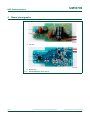
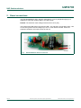
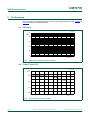
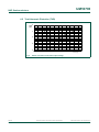
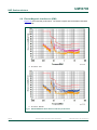
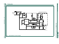
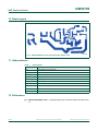
UM10793 SSL5031BDB1207 120 V 9 W buck converter Rev. 1 — 20 October 2014 User manual Document information Info Content Keywords SSL5031BDB1207, SSL5031BTS, non-dimmable, LED driver, buck converter, A19 Abstract This user manual describes the operation of the SSL5031BDB1207 120 V 9 W non-dimmable LED driver featuring the SSL5031BTS. The demo board uses a buck topology. It has a form factor that is compatible with the base of a A19 LED lamp fitting used in Solid-State Lighting (SSL) applications. UM10793 NXP Semiconductors SSL5031BDB1207 120 V 9 W buck converter Revision history Rev Date Description v.1 20141020 first issue Contact information For more information, please visit: http://www.nxp.com For sales office addresses, please send an email to: [email protected] UM10793 User manual All information provided in this document is subject to legal disclaimers. Rev. 1 — 20 October 2014 © NXP Semiconductors N.V. 2014. All rights reserved. 2 of 16 UM10793 NXP Semiconductors SSL5031BDB1207 120 V 9 W buck converter 1. Introduction WARNING Lethal voltage and fire ignition hazard The non-insulated high voltages that are present when operating this product, constitute a risk of electric shock, personal injury, death and/or ignition of fire. This product is intended for evaluation purposes only. It shall be operated in a designated test area by personnel qualified according to local requirements and labor laws to work with non-insulated mains voltages and high-voltage circuits. This product shall never be operated unattended. This user manual describes the operation of the SSL5031BDB1207 120 V 9 W eco-THD non-dimmable LED driver featuring the SSL5031BTS. The reference board has a A19 LED lamp compatible form factor. The buck converter topology provides a simple and efficient solution for mains non-dimmable LED recessed light applications. The reference board complies with EMI and safety regulations. Figure 2 shows the dimensions of the SSL5031BDB1207 demo board. The design of the board allows enough headroom for the board to fit into a A19 lamp base. Figure 3 shows the SSL5031BDB1207 assembled top and bottom views. 2. Safety warning The demo board input is connected to the 120 V mains supply. Avoid touching the board while it is connected to the mains voltage and when it is in operation. An isolated housing is obligatory when used in uncontrolled, non-laboratory environments. Galvanic isolation from the mains phase using a fixed or variable transformer is always recommended. Figure 1 shows the symbols on how to recognize these devices. 019aab174 019aab173 a. Isolated Fig 1. UM10793 User manual b. Not isolated Isolation symbols All information provided in this document is subject to legal disclaimers. Rev. 1 — 20 October 2014 © NXP Semiconductors N.V. 2014. All rights reserved. 3 of 16 UM10793 NXP Semiconductors SSL5031BDB1207 120 V 9 W buck converter 3. Specifications Table 1 lists the specification of the SSL5031BDB1207 demo board. Table 1. SSL5031BDB1207 specifications Symbol Parameter Value Vmains AC mains supply voltage 120 V (AC); 10 % Imains AC mains input current 80 mA VLED output voltage 40 V ILED output current 205 mA ILED(ripple) output current ripple < 30 % ILED/Vmains line rejection <2% ILED/VLED output voltage rejection <1% efficiency > 88 %; at 120 V (AC)/60 Hz PF power factor > 0.95 THD total harmonic distortion < 20 % Toper operating temperature 40 C to +100 C fsw switching frequency 60 kHz to 160 kHz tstartup start-up time 120 ms Figure 2 shows the dimensions of the demo board. Fig 2. UM10793 User manual SSL5031BDB1207 demo board dimensions All information provided in this document is subject to legal disclaimers. Rev. 1 — 20 October 2014 © NXP Semiconductors N.V. 2014. All rights reserved. 4 of 16 UM10793 NXP Semiconductors SSL5031BDB1207 120 V 9 W buck converter 4. Board photographs a. Top view b. Bottom view Fig 3. UM10793 User manual SSL5031BDB1207 demo board All information provided in this document is subject to legal disclaimers. Rev. 1 — 20 October 2014 © NXP Semiconductors N.V. 2014. All rights reserved. 5 of 16 UM10793 NXP Semiconductors SSL5031BDB1207 120 V 9 W buck converter 5. Board connections The SSL5031BDB1207 demo board is optimized for a 120 V (AC)/60 Hz supply. It is designed to work with multiple LEDs or an LED module. Remark: The maximum rated voltage of the board is 132 V (AC). The anode of the LED load is connected to LED+. The cathode is connected to LED-. Use an LED string with a forward voltage up to 40 V on this reference board. Under the expected conditions, the output current is 205 mA. Fig 4. UM10793 User manual SSL5031BDB1207 board connections All information provided in this document is subject to legal disclaimers. Rev. 1 — 20 October 2014 © NXP Semiconductors N.V. 2014. All rights reserved. 6 of 16 UM10793 NXP Semiconductors SSL5031BDB1207 120 V 9 W buck converter 6. Performance The performance was measured with a 40 V at an LED output load of 205 mA. Figure 5 to Figure 10 show the performance data. 6.1 Efficiency DDD Ș Fig 5. 9PDLQV9 Efficiency as a function of mains voltage 6.2 Power Factor (PF) DDD 3) Fig 6. UM10793 User manual 9PDLQV9 PF as a function of mains voltage All information provided in this document is subject to legal disclaimers. Rev. 1 — 20 October 2014 © NXP Semiconductors N.V. 2014. All rights reserved. 7 of 16 UM10793 NXP Semiconductors SSL5031BDB1207 120 V 9 W buck converter 6.3 Line regulation DDD ,/(' $ Fig 7. 9PDLQV9 LED current as a function of mains voltage 6.4 Load regulation DDD ,/(' $ Fig 8. UM10793 User manual 9/('9 LED current as a function of LED voltage All information provided in this document is subject to legal disclaimers. Rev. 1 — 20 October 2014 © NXP Semiconductors N.V. 2014. All rights reserved. 8 of 16 UM10793 NXP Semiconductors SSL5031BDB1207 120 V 9 W buck converter 6.5 Total Harmonic Distortion (THD) DDD 7+' Fig 9. UM10793 User manual 9PDLQV9 THD as a function of AC mains input voltage All information provided in this document is subject to legal disclaimers. Rev. 1 — 20 October 2014 © NXP Semiconductors N.V. 2014. All rights reserved. 9 of 16 UM10793 NXP Semiconductors SSL5031BDB1207 120 V 9 W buck converter 6.6 ElectroMagnetic Interference (EMI) Figure 10 shows the EMI performance. The board complies with the EN55015 standard requirements. a. AC mains - Line b. AC mains - Neutral Fig 10. SSL5031BDB1207 demo board conduction performance UM10793 User manual All information provided in this document is subject to legal disclaimers. Rev. 1 — 20 October 2014 © NXP Semiconductors N.V. 2014. All rights reserved. 10 of 16 UM10793 NXP Semiconductors SSL5031BDB1207 120 V 9 W buck converter 7. Protections The IC incorporates the following protections: • • • • • • UnderVoltage LockOut (UVLO) OverCurrent Protection (OCP) Output Short Protection (OSP) Output open OverVoltage Protection (OVP) Internal OverTemperature Protection (OTP) External thermal foldback (optional) All protections are not latched and lead to a safe restart of the converter. For more information about protections, see the SSL5031BTS data sheet (Ref. 1). UM10793 User manual All information provided in this document is subject to legal disclaimers. Rev. 1 — 20 October 2014 © NXP Semiconductors N.V. 2014. All rights reserved. 11 of 16 xxxxxxxxxxxxxxxxxxxxx xxxxxxxxxxxxxxxxxxxxxxxxxx xxxxxxx x x x xxxxxxxxxxxxxxxxxxxxxxxxxxxxxx xxxxxxxxxxxxxxxxxxx xx xx xxxxx xxxxxxxxxxxxxxxxxxxxxxxxxxx xxxxxxxxxxxxxxxxxxx xxxxxx xxxxxxxxxxxxxxxxxxxxxxxxxxxxxxxxxxx xxxxxxxxxxxx x x xxxxxxxxxxxxxxxxxxxxx xxxxxxxxxxxxxxxxxxxxxxxxxxxxxx xxxxx xxxxxxxxxxxxxxxxxxxxxxxxxxxxxxxxxxxxxxxxxxxxxxxxxx xxxxxxxx xxxxxxxxxxxxxxxxxxxxxxxxx xxxxxxxxxxxxxxxxxxxx xxx NXP Semiconductors UM10793 User manual 8. Schematic )5 / %' 0%6 - ,1387 : 9$& +] 029 .' RSWLRQDOFLUFXLWIRU293WRXVHDQ RXWSXWFDSDFLWRURIORZHUUDWHGYROWDJH / P+ 5 1 & Q) 9 5 Nȍ & Q) 9 5 QP ' 1 8 &203 & Q) 9 *1' ,616 QP ȍ 0 6361& '(0293 5 QP =' QP 5 Nȍ 5 ' (6- ' QP 6: ȍ ' 5 9&& & ) 9 66/ & QP 5 ȍ / 5 Nȍ /(' + & ) 9 5 Nȍ 287387 9 P$ DDD Fig 11. SSL5031BDB1207 schematic diagram UM10793 12 of 16 © NXP Semiconductors N.V. 2014. All rights reserved. /(' SSL5031BDB1207 120 V 9 W buck converter Rev. 1 — 20 October 2014 All information provided in this document is subject to legal disclaimers. Nȍ UM10793 NXP Semiconductors SSL5031BDB1207 120 V 9 W buck converter 9. Bill Of Materials (BOM) Table 2. SSL5031BDB1207 bill of materials Reference Description and values Part number Manufacturer BD1 bridge rectifier; 600 V; 500 mA; MBS-1 MB6S MCC C1 capacitor; 1 F; 25 V; 0603 GRM188R71E105KA12D Murata C2; C3 capacitor; film; 150 nF; 250 V; CL21; pitch = 7.5 mm - - C4 capacitor; 220 nF; 25 V; 0603 GRM188R71E224KA88D Murata C5 capacitor; 220 F; 63 V; pitch = 5 mm; 10 mm 16 mm OLKE21J221MF Shanghai Yongming Electronics C6 capacitor; not mounted - - D2 diode; ultrafast; 600 V; 1 A; SMA ES1J Taiwan Semiconductor D3 diode; ultrafast; 75 V; 150 mA; SOD323 1N4148 DiodesZetex D4; D5 diode; not mounted - - FR1 fuse resistor; 10 ; 2 W; 5 % RF10-2W10J TY-OHM L1 inductor; 2.2 mH; Isat = 0.16 A; pitch = 3 mm; 6 mm 8 mm DR0608-222 A KEE L2 inductor; 680 H; Isat = 0.6 A; pitch = 5 mm; 8 mm 10 mm 744 772 681 Würth Elektronik M1 MOSFET; RDSon = 6 ; Id = 0.8 A; Vds = 650 V; TO-251 SPS01N60C3 Infineon MOV1 varistor; 150 V (AC); 200 V (DC); = 7 mm 241KD07 BrightKing R1 resistor; 300 k; 5 %; 1206 - - R3 resistor; 10 k; 5 %; 1206 - - R4 resistor; 162 k; 1 %; 1206 - - R6 resistor; 5.62 k; 1 %; 0603 - - R7 resistor; 220 ; 5 %; 1206 - - R8; R9 resistor; 3.9 ; 1 %; 1206 - - R10 resistor; 39 k; 5 %; 1206 - - R11; R12 resistor; not mounted - - U1 controller; TSOP6 SSL5031BTS NXP Semiconductors ZD6 diode; Zener; not mounted - - UM10793 User manual All information provided in this document is subject to legal disclaimers. Rev. 1 — 20 October 2014 © NXP Semiconductors N.V. 2014. All rights reserved. 13 of 16 UM10793 NXP Semiconductors SSL5031BDB1207 120 V 9 W buck converter 10. Board layout Fig 12. SSL5031BDB1207 demo board assembly, bottom view 11. Abbreviations Table 3. Abbreviations Acronym Description EMI ElectroMagnetic Interference LED Light-Emitting Diode OCP OverCurrent Protection OSP Output Short Protection OTP OverTemperature Protection OVP OverVoltage Protection PF Power Factor SSL Solid-State Lighting THD Total Harmonic Distortion UVLO UnderVoltage LockOut 12. References [1] UM10793 User manual SSL5031BTS data sheet — Compact high power factor/low-THD buck LED driver IC All information provided in this document is subject to legal disclaimers. Rev. 1 — 20 October 2014 © NXP Semiconductors N.V. 2014. All rights reserved. 14 of 16 UM10793 NXP Semiconductors SSL5031BDB1207 120 V 9 W buck converter 13. Legal information 13.1 Definitions Draft — The document is a draft version only. The content is still under internal review and subject to formal approval, which may result in modifications or additions. NXP Semiconductors does not give any representations or warranties as to the accuracy or completeness of information included herein and shall have no liability for the consequences of use of such information. NXP Semiconductors does not accept any liability related to any default, damage, costs or problem which is based on any weakness or default in the customer’s applications or products, or the application or use by customer’s third party customer(s). Customer is responsible for doing all necessary testing for the customer’s applications and products using NXP Semiconductors products in order to avoid a default of the applications and the products or of the application or use by customer’s third party customer(s). NXP does not accept any liability in this respect. Export control — This document as well as the item(s) described herein may be subject to export control regulations. Export might require a prior authorization from competent authorities. 13.2 Disclaimers Limited warranty and liability — Information in this document is believed to be accurate and reliable. However, NXP Semiconductors does not give any representations or warranties, expressed or implied, as to the accuracy or completeness of such information and shall have no liability for the consequences of use of such information. NXP Semiconductors takes no responsibility for the content in this document if provided by an information source outside of NXP Semiconductors. In no event shall NXP Semiconductors be liable for any indirect, incidental, punitive, special or consequential damages (including - without limitation - lost profits, lost savings, business interruption, costs related to the removal or replacement of any products or rework charges) whether or not such damages are based on tort (including negligence), warranty, breach of contract or any other legal theory. Notwithstanding any damages that customer might incur for any reason whatsoever, NXP Semiconductors’ aggregate and cumulative liability towards customer for the products described herein shall be limited in accordance with the Terms and conditions of commercial sale of NXP Semiconductors. Right to make changes — NXP Semiconductors reserves the right to make changes to information published in this document, including without limitation specifications and product descriptions, at any time and without notice. This document supersedes and replaces all information supplied prior to the publication hereof. Suitability for use — NXP Semiconductors products are not designed, authorized or warranted to be suitable for use in life support, life-critical or safety-critical systems or equipment, nor in applications where failure or malfunction of an NXP Semiconductors product can reasonably be expected to result in personal injury, death or severe property or environmental damage. NXP Semiconductors and its suppliers accept no liability for inclusion and/or use of NXP Semiconductors products in such equipment or applications and therefore such inclusion and/or use is at the customer’s own risk. Applications — Applications that are described herein for any of these products are for illustrative purposes only. NXP Semiconductors makes no representation or warranty that such applications will be suitable for the specified use without further testing or modification. Customers are responsible for the design and operation of their applications and products using NXP Semiconductors products, and NXP Semiconductors accepts no liability for any assistance with applications or customer product design. It is customer’s sole responsibility to determine whether the NXP Semiconductors product is suitable and fit for the customer’s applications and products planned, as well as for the planned application and use of customer’s third party customer(s). Customers should provide appropriate design and operating safeguards to minimize the risks associated with their applications and products. Evaluation products — This product is provided on an “as is” and “with all faults” basis for evaluation purposes only. NXP Semiconductors, its affiliates and their suppliers expressly disclaim all warranties, whether express, implied or statutory, including but not limited to the implied warranties of non-infringement, merchantability and fitness for a particular purpose. The entire risk as to the quality, or arising out of the use or performance, of this product remains with customer. In no event shall NXP Semiconductors, its affiliates or their suppliers be liable to customer for any special, indirect, consequential, punitive or incidental damages (including without limitation damages for loss of business, business interruption, loss of use, loss of data or information, and the like) arising out the use of or inability to use the product, whether or not based on tort (including negligence), strict liability, breach of contract, breach of warranty or any other theory, even if advised of the possibility of such damages. Notwithstanding any damages that customer might incur for any reason whatsoever (including without limitation, all damages referenced above and all direct or general damages), the entire liability of NXP Semiconductors, its affiliates and their suppliers and customer’s exclusive remedy for all of the foregoing shall be limited to actual damages incurred by customer based on reasonable reliance up to the greater of the amount actually paid by customer for the product or five dollars (US$5.00). The foregoing limitations, exclusions and disclaimers shall apply to the maximum extent permitted by applicable law, even if any remedy fails of its essential purpose. Safety of high-voltage evaluation products — The non-insulated high voltages that are present when operating this product, constitute a risk of electric shock, personal injury, death and/or ignition of fire. This product is intended for evaluation purposes only. It shall be operated in a designated test area by personnel that is qualified according to local requirements and labor laws to work with non-insulated mains voltages and high-voltage circuits. The product does not comply with IEC 60950 based national or regional safety standards. NXP Semiconductors does not accept any liability for damages incurred due to inappropriate use of this product or related to non-insulated high voltages. Any use of this product is at customer’s own risk and liability. The customer shall fully indemnify and hold harmless NXP Semiconductors from any liability, damages and claims resulting from the use of the product. Translations — A non-English (translated) version of a document is for reference only. The English version shall prevail in case of any discrepancy between the translated and English versions. 13.3 Trademarks Notice: All referenced brands, product names, service names and trademarks are the property of their respective owners. GreenChip — is a trademark of NXP Semiconductors N.V. UM10793 User manual All information provided in this document is subject to legal disclaimers. Rev. 1 — 20 October 2014 © NXP Semiconductors N.V. 2014. All rights reserved. 15 of 16 UM10793 NXP Semiconductors SSL5031BDB1207 120 V 9 W buck converter 14. Contents 1 2 3 4 5 6 6.1 6.2 6.3 6.4 6.5 6.6 7 8 9 10 11 12 13 13.1 13.2 13.3 14 Introduction . . . . . . . . . . . . . . . . . . . . . . . . . . . . 3 Safety warning . . . . . . . . . . . . . . . . . . . . . . . . . . 3 Specifications. . . . . . . . . . . . . . . . . . . . . . . . . . . 4 Board photographs . . . . . . . . . . . . . . . . . . . . . . 5 Board connections . . . . . . . . . . . . . . . . . . . . . . 6 Performance . . . . . . . . . . . . . . . . . . . . . . . . . . . . 7 Efficiency . . . . . . . . . . . . . . . . . . . . . . . . . . . . . 7 Power Factor (PF) . . . . . . . . . . . . . . . . . . . . . . 7 Line regulation . . . . . . . . . . . . . . . . . . . . . . . . . 8 Load regulation . . . . . . . . . . . . . . . . . . . . . . . . . 8 Total Harmonic Distortion (THD). . . . . . . . . . . . 9 ElectroMagnetic Interference (EMI) . . . . . . . . 10 Protections . . . . . . . . . . . . . . . . . . . . . . . . . . . . 11 Schematic . . . . . . . . . . . . . . . . . . . . . . . . . . . . . 12 Bill Of Materials (BOM) . . . . . . . . . . . . . . . . . . 13 Board layout . . . . . . . . . . . . . . . . . . . . . . . . . . . 14 Abbreviations . . . . . . . . . . . . . . . . . . . . . . . . . . 14 References . . . . . . . . . . . . . . . . . . . . . . . . . . . . 14 Legal information. . . . . . . . . . . . . . . . . . . . . . . 15 Definitions . . . . . . . . . . . . . . . . . . . . . . . . . . . . 15 Disclaimers . . . . . . . . . . . . . . . . . . . . . . . . . . . 15 Trademarks. . . . . . . . . . . . . . . . . . . . . . . . . . . 15 Contents . . . . . . . . . . . . . . . . . . . . . . . . . . . . . . 16 Please be aware that important notices concerning this document and the product(s) described herein, have been included in section ‘Legal information’. © NXP Semiconductors N.V. 2014. All rights reserved. For more information, please visit: http://www.nxp.com For sales office addresses, please send an email to: [email protected] Date of release: 20 October 2014 Document identifier: UM10793