1
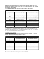
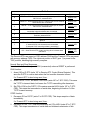
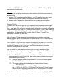
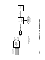
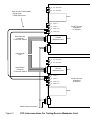
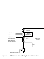
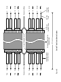
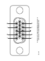
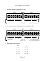
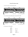
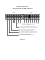
User Manual for Serial Test Cards
University of Wisconsin - Madison
Phil Robl
UW Physical Sciences Laboratory
Introduction
Receiver Card
Receiver Cards were developed at the University of Wisconsin as part of the Regional
Calorimeter Trigger for the CMS detector. Each Receiver Card is designed to receive 32
high speed copper serial links from the calorimeter readout electronics. Each link
transmits either two towers of hadronic or electromagnetic information per crossing for a
total of 64 channels from 32 ECAL and 32 HCAL towers per card. Each of the 32 serial
links uses differential PECL signals and runs at a rate of 1.2Gb/s.
Receiver Mezzanine Card
The 32 links are bundled in groups of four and routed to 8 Receiver Mezzanine Cards
plugged into the back of a Receiver Card. Each Receiver Mezzanine Card contains a
Vitesse 7216 4-channel Interconnect Chip. In addition to developing the Receiver
Mezzanine Cards, UW engineers developed a Transmit Mezzanine Card, also based on
the Vitesse 7216 and capable of transmitting 4 channels (links) of serial data at 1.2Gb/s.
Serial Test Card
Finally, a Serial Test Card was developed to test the functionality of the Receiver
Mezzanine Cards and to measure their Bit Error Rate (BER). This document describes
the Serial Test Card.
Functional Description
The Serial Test Card (STC) may be configured either as a Transmit STC or as a
Receive STC. A Transmit STC contains one Transmit Mezzanine Card only. A Receive
STC contains one Receive Mezzanine Card only. The STC was not designed for
simultaneous operation of both a Transmit and a Receive Mezzanine Card. A simple set
of soldered jumpers configures an STC into be either Transmit or Receive.
Transmit STC Function
Refer to Figure 1, "Transmit Serial Test Card Block Diagram". Each STC contains two
16K x 32-bit memories -- a transmit memory and a receive memory. Configured as
Transmit, the STC sends a continuous serial stream from the 16K deep transmit
memory. The receive memory is not used. At each positive transition of the 120MHz
clock, a new 32-bit word is sent out over four 8-bit/10-bit serial channels. The address
counter rolls over every 16K counts, so the memory is transmitted over and over in a
continuous loop. The memory is loaded through a VME interface, and may be read back
through VME. The VME interface cannot access memory while serial data is being
transmitted.
Receive STC Function
Refer to Figure 2, "Receive Serial Test Card Block Diagram". Configured as Receive,
the STC receives a continuous serial stream from serial data lines. This data is
continuously written to the receive memory. At the same time, a copy of the transmit
memory on the Transmit STC is stored in the transmit memory of the Receive STC. The
data from this copy is sent to fast 32-bit compare circuitry along with the transient
incoming receive data. A 32-bit comparison is done on the fly (using four 8-bit
MC100E166 comparators) and receive processing is halted if any bit does not match. In
addition the Receive STC reports link status from the Vitesse 7216 4-channel
Interconnect Chip, and will halt on link errors. If processing is halted due to an error -data or link -- a VME readable flag is set. Three status registers are used. One contains
the stop flag, one contains the link status bits for all four channels captured at the time
the error occurred, and the other points indirectly to the location in receive memory
where the data was captured at the time the error occurred.
Installation
The STC is a 9U VME board. Refer to Figure 3, "STC Interconnections For Testing
Receive Mezzanine Card" for a simplified scale drawing of both Transmit and Receive
STCs. The STC is oversized in depth (11") and will extend beyond the normal front
panel in a standard VME crate.
VME Crate Cooling Fans
It is absolutely necessary that the VME crate be equipped with cooling fans that run
whenever crate power is on. The 3.3V Vicor DC-DC converter may overheat if forced air
cooling is not provided.
Testing the Receive STC and Receive Mezzanine Card
To test the Receive STC and Receive Mezzanine Card themselves, a Transmit STC
with Transmit Mezzanine Card must be installed. Refer to Figure 3, "STC
Interconnections For Testing Receive Mezzanine Card". Connect short (1m or less),
equal length 50Ω coaxial cables with LEMO connectors between Transmit STC and
Receive STC as shown (Transmit J3 to Receive J1, Transmit J4 to Receive J2). Switch
SW1, position 3, on the Receive STC must be set to ON. The same switch on the
Transmit STC should be set to OFF if its internal oscillator is to be used to clock both
boards. Connect the supplied serial cable between the 15-socket connector on the
Transmit Mezzanine Card to the same connector on the Receive Mezzanine Card. The
cable and pinouts are documented in figures 5 and 6.
Testing a User-Supplied Serial Transmitter
To test a user-supplied serial transmitter, a single Receive STC would be installed.
Refer to Figure 4, "STC Interconnections For Testing User's Serial Transmitter". In this
case it is assumed that the Receive STC and Receive Mezzanine Card are functioning
properly. An external differential 120MHz clock must be supplied to the Receive STC
through LEMO connectors J1 (Clock In +) and J2 (Clock In –), and switch SW1, position
3, must be set to ON. The clock must be phase locked to the clock used to transmit
serial data. The clocks must be ECL or PECL (~900mV swing). Both clock lines are
capacitor coupled behind the LEMO connector, and terminated with 51Ω to ground on
the other side of the capacitor. See the sheet BLOCK: CLK_GEN of the Serial Test
Card drawing set. LEMO connectors J3 and J4 as well as J5 and J6 provide differential,
capacitor coupled ECL/PECL level clock output signals. The serial data is delivered to
J1 on the Receive Mezzanine Card through user-supplied cable. The serial signals must
terminate in a male 15-pin HD-22 high density D connector (AMP 748364-1 or
equivalent). Connections are documented in figure 6 and a suggested cable is
documented in figure 5.
Additional STCs
Additional STCs may be installed in the same crate so long as they have unique
addresses and the +48Vdc supply can handle them.
Power Connections and Power Control
Refer to Figure 7, "Power Wiring for Serial Test Cards". Connect +48Vdc power and
control wires to the first (or only) Receive STC as shown. Connect +48Vdc as shown to
all other STCs in the crate -- Transmit or Receive. The STC requires 3 dc voltages:
+3.3V, –2.0V, and +5V. The +48Vdc powers two Vicor dc–dc converters, +3.3V and
–2.0V. +5Vdc is taken from the VME crate power supply, and it is used to activate the
+48Vdc by way of a solid state relay. In this way the +48Vdc will not be present on the
STC when the crate power is turned off.
Power Supply
The +48Vdc power supply must be capable of delivering at least 1.5A per STC, so a
150W supply is just adequate for two STCs. A 200W is recommended. Precautions
should be taken to shield all 120/240VAC connections to reduce shock hazard.
Memory and Control Status Registers
Memory
Each STC contains two 16K x 32-bit memories -- a transmit memory and a receive
memory. The memories are mapped to VME address space via dip switches that cover
VME address bits A23-A17 (optionally A31-A17). If the upper VME address matches the
dip switches and if A16=0, the receive memory is accessed by VME address bits
A15-A2. Alternately if A16=1, the transmit memory is accessed by the same address
bits A15-A2. VME addressing for the STC is always 32 bit, so the lowest two address
bits (A1-A0) are not used.
VME addressing of STC memories is summarized in Table 1 below. In Table 1,
remember that VME addresses increment by 4 since VME address bits A1-A0 are
always zero. The upper address byte (shown here as the preset value, "FA") is not
required if the rightmost position of SW7 (pos. 1) is in the "ON" position. See "Switches
and Jumpers" section below.
For all switches in SW5-SW8: Up = OFF = logic 1, Down = ON = logic 0.
Table 1
Memory Base Address
Examples (SW5 & SW7)
.
.
.
Receive Memory Range
16K 32-bit Words
Transmit Memory Range
16K 32-bit Words
FA80
FA800000, FA800004, FA800008,
FA80000C .... to FA80FFFC
FA810000, FA810004, FA810008,
FA81000C .... to FA81FFFC
FA82
FA820000 to FA82FFFC
FA830000 to FA83FFFC
FA84
.
.
.
FAC0
FA840000 to FA84FFFC
FA850000 to FA85FFFC
FAC00000 to FAC0FFFC
FAC10000 to FAC1FFFC
FAC2
FAC20000 to FAC2FFFC
FAC30000 to FAC3FFFC
FAC4
.
.
.
FAC40000 to FAC4FFFC
FAC50000 to FAC5FFFC
The Receive STCs are preset at memory address FA80 and the Transmit STCs are
preset with memory address FAC0. The rightmost position of SW7 (pos. 1) is preset in
the "ON" position, disabling high memory compare.
Control and Status Registers
Each STC also contains one 9-bit control register (write only) and three 16-bit status
registers (read only). Addressing is shown in Table 2.
Table 2
CSR Base Address
Examples (SW6 & SW8)
.
.
.
FA90
Control Register (write only)
Status Registers (read only)
FA900000
FA900020, FA900024, FA900028
FA92
FA920000
FA920020, FA920024, FA920028
FA94
.
.
.
FAD0
.
.
.
FA940000
FA940020, FA940024, FA940028
FAD00000
FAD00020, FAD00024, FAD00028
The meaning of the 9-bit control register is shown in Table 3.
Table 3
Bit
Action
Applies to
0
TRSTN -- JTAG Test Access Port test logic reset input of Vitesse
VSC7216-01; asserted LOW
Receive STC
1
RESETN -- When asserted LOW, the Vitesse VSC7216-01 receiver
elastic buffers are re-centered
Receive STC
2
TRSTN -- JTAG Test Access Port test logic reset input of Vitesse
VSC7216-01; asserted LOW
Transmit STC
3
RESETN -- When asserted LOW, the Vitesse VSC7216-01
transmitter input skew buffers are re-centered
Transmit STC
4
WSENn -- Word Sync Enable for all four Vitesse VSC7216-01
channels; asserted HIGH
Transmit STC
5
Spare 1
6
Spare 0
7
C/Dn -- Control/Data for all four Vitesse VSC7216-01 channels
If asserted HIGH, idle characters are transmitted
If asserted LOW, transmit port data is transmitted
Transmit STC
8
GO -- Starts transmission of data on Transmit STC
GO -- Arms Receive STC to start receiving when it detects data
characters
Receive STC
Transmit STC
The Receive STCs are preset at CSR address FA90 and the Transmit STCs are preset
with memory address FAD0. The rightmost position of SW7 (pos. 1) is preset in the
"ON" position, disabling high memory compare.
Normal Start and Stop Sequences
Note that bits 0-3 are always set HIGH (unasserted) unless a RESET is performed.
RUN function:
1. Assert GO on R-STC (write 10F to Receive STC Control Status Register). This
arms the R-STC to receive data when the first non-idle character is seen.
If a Transmit STC is also being used, then:
2. Assert GO on T-STC, but leave C/Dn HIGH (write 18F to T-STC CSR). This arms
the T-STC to transmit data, but leaves the T-STC transmitting idle characters.
3. Set C/Dn LOW on the R-STC; GO remains asserted HIGH (write 10F to T-STC
CSR). This starts the transmission of serial data, beginning at location 0 of the
T-STC transmit memory.
STOP function:
1. De-assert GO on R-STC (write F to R-STC CSR). This stops reception of data
immediately.
If a Transmit STC is also being used, then:
2. De-assert GO on T-STC and simultaneously set C/Dn HIGH (write 8F to T-STC
CSR). This stops transmission of serial data and initiates transmission of idle
characters.
RESET function:
1. Clear RESETN and TRSTN bits on R-STC, while leaving GO cleared (write 0 to
R-STC CSR). This asserts the receive RESETN while leaving R-STC stopped.
2. Set RESETN and TRSTN bits on R-STC, while leaving GO cleared (write F to
R-STC CSR). This de-asserts the receive RESETN while leaving R-STC stopped.
If a Transmit STC is also being used, then:
3. Clear RESETN and TRSTN bits on T-STC, leave GO cleared and C/Dn HIGH (write
80 to T-STC CSR). This asserts transmit RESETN, but keeps T-STC stopped.
4. Set RESETN and TRSTN bits on T-STC, leave GO cleared and C/Dn HIGH (write
8F to T-STC CSR). This de-asserts transmit RESETN, but keeps T-STC stopped.
The three 16-bit receive status registers are shown in Table 4. Status registers have
little meaning for Transmit, so only Receive is shown. Receive CSR address is FA90.
Table 4
Register
Bits
Meaning
FA900020
00
ERRA of Vitesse VSC7216-01 receiver
"
01
IDLEA of Vitesse VSC7216-01 receiver
"
02
KCHA of Vitesse VSC7216-01 receiver
"
03
0
"
04
ERRB of Vitesse VSC7216-01 receiver
"
05
IDLEB of Vitesse VSC7216-01 receiver
"
06
KCHB of Vitesse VSC7216-01 receiver
"
07
0
"
08
ERRC of Vitesse VSC7216-01 receiver
"
09
IDLEC of Vitesse VSC7216-01 receiver
"
10
KCHC of Vitesse VSC7216-01 receiver
"
11
0
"
12
ERRD of Vitesse VSC7216-01 receiver
"
13
IDLED of Vitesse VSC7216-01 receiver
"
14
KCHD of Vitesse VSC7216-01 receiver
"
15
0
"
16-31
Indeterminate
FA900024
00-13
120MHz address counter -- latched upon hardware stop
"
14-15
0
FA900028
00-07
Memory base address as set by SW7
"
08
Error Stop
"
11
One-Shot Stop
"
09, 10, 12-15
0
See Vitesse VSC7216-01 documentation for a description of ERR, IDLE, and KCH, and
their meaning in combination.
Power Up
After power-up and before attempting any other operation, the following sequence is
recommended:
1. Issue a STOP sequence as defined above. The STC usually powers up in serial
transmission run mode and must be stopped to load memories from VME.
2. Issue a RESET sequence as defined above. This re-centers all serial buffers.
Receive STC Halt
A Receive STC halt occurs when the STC stops itself from processing incoming data.
This can be detected during RUN mode by polling bit 8 of the 3rd status register (Error
Stop -- see Table 4). It can also be detected during RUN mode by repeatedly polling the
120MHz address counter (bits 00-13 of the 2nd status register -- Table 4) and observing
that they continually change. They will stop changing after a halt. For either method of
halt detection, it is assumed that SW1 position 6 is OFF. Refer to figure 10 for a
description of switches SW1 and SW2.
After a Receive STC has halted, and before attempting any operation other than
reading registers, issue a STOP sequence as defined above. A STOP must be issued
before a RUN can be re-issued.
If SW1 position 2 is ON, One-Shot operation is enabled. In this case, bit 11 of the 3rd
status register should be asserted on halt, along with bit 8. Bit 11 indicates a successful
one-shot fill of memory. If bit 11 is not set, it probably means an error halted the
Receive STC before memory was filled.
After a Receive STC has halted, the source of the halt can be determined in the
following manner, assuming one-shot stop is disabled (SW1 position 2 is OFF) and
heads-up readout is captured after a halt (SW1 position 6 is OFF):
1. If a data NOT EQUAL error has occurred, the Receive STC receive memory should
have captured the corrupt 32-bit word. The receive memory address of the corrupt
word can be found as follows:
1.1.
Read the captured address count from bits 0-13 of the 2nd status register
(see Table 4). Call this address Ac.
1.2.
The memory address Am can be derived with the following formula:
Am = 4(Ac - 4)
For example, if the address count Ac = 1FC5 (hex), then the memory address
Am = 4(1FC5 - 4) = 4(1FC1) = 7F04 (hex). If the Receive STC base memory
address is FA80, then this corresponds to a full 32-bit Receive STC receive
memory address of FA807F04.
2. If a Vitesse receive error is not seen in the 1st status register (any if the four ERRn
bits -- see Table 4) then the error is a data NOT EQUAL error. Examination of
Receive STC receive memory should elucidate the data error.
3. If a Vitesse receive error is seen in the 1st status register, then it may or may not be
accompanied by a data NOT EQUAL error. Again, examination of Receive STC
receive memory should indicate any data compare errors.
Switches and Jumpers
Figures 8 and 9 show DIP switch presets for Transmit and Receive STCs for Memory
and CSR. The functions of SW5-SW8 are described above. The figures also show
soldered jumpers required to configure an STC to be either Transmit or Receive (SW3
and SW4). Figure 10 documents the special function and delay switches SW1 and
SW2.
Comparing VME Addresses 31-24 To Access STC Memory (SW5 and SW7)
The rightmost position of SW7, position 1, controls whether the upper address bits
31-24 are included in the STC address comparison. If SW7, pos. 1 is down (ON) then
all 15 VME address bits 31-17 will be compared to the respective setting on SW5 and
SW7.
If SW7, pos. 1 is up (OFF) then only VME address bits 23-17 will be compared to the
respective setting on SW7. For this mode to work properly, it is critical that the upper
VME address bits (31-24) not match the DIP switch settings on SW5. Choose an
address setting for DIP switch SW5 that is always unused.
Comparing VME Addresses 31-24 To Access CSR Registers (SW6 and SW8)
The rightmost position of SW8 (position 1), controls whether the upper address bits
31-24 are included in the STC address comparison. If SW8, pos. 1 is down (ON) then
all 15 VME address bits 31-17 will be compared to the respective setting on SW6 and
SW8.
If SW8, pos. 1 is up (OFF) then only VME address bits 23-17 will be compared to the
respective setting on SW8. For this mode to work properly, it is critical that the upper
VME address bits (31-24) not match the DIP switch settings on SW6. Choose an
address setting for DIP switch SW6 that is always unused.
Clock Source, Stop Settings, and Board Delay (SW1 and SW2)
1. NOT EQUAL Error, SW1 position 1 (Receive STC only)
1.1.
If NOT EQUAL error stop is enabled (ON), a Receive STC will halt if the
incoming serial data is not identical to the corresponding data read out from
memory. This is the normal operating mode. A STOP sequence as defined
above should be issued after a halt is detected.
1.2.
If NOT EQUAL error stop is disabled (OFF), a Receive STC will not halt as a
result of data errors. This is for diagnostic purposes. A Receive STC will still
halt if:
1.2.1. An ERR receiver error is asserted for any receive channel, and
1.2.2. The receive error jumpers are installed in SW3
2. One-Shot Stop, SW1 position 2 (Receive STC only)
2.1.
If One-Shot Stop is enabled (ON), the Receive STC will fill its memory once
with the "leading edge" of the incoming data, then stop. This is for diagnostic
purposes. It will not fill all of memory if a halt occurs, so disabling NOT
EQUAL error stop at the same time is a good idea.
2.2.
If One-Shot Stop is enabled (ON), the Receive STC functions normally.
3. System Clock Source, SW1 position 3
3.1.
If ON, board clock is derived from external differential ECL inputs. See the
paragraph Testing a User-Supplied Serial Transmitter for details. A Receive
STC must be in this mode because it requires an external clock synchronized
to the incoming serial data. A Transmit STC may be in this mode if it is to be
synchronized with a system clock.
3.2.
If OFF, board clock is derived from a local 120MHz low drift, low jitter
oscillator. This is only an option for a Transmit STC, and allows stand-alone
operation.
4. "Heads-Up" Readout, SW1 position 6 (Receive STC only). The Heads-Up readout
is comprised of the three 16-bit receive status registers shown in Table 4.
4.1.
If OFF, the first two "Heads-Up" registers (shown as FA900020 and
FA900024 in table 4) are captured after an error halt or a stop command. The
third register (shown as FA900028 in table 4) is always live. This is the
normal mode of operation.
4.2.
If ON, the all three "Heads-Up" registers are live at all times. This mode is for
diagnostic purposes.
5. Delay Setting, SW1 positions 7 and 8 plus SW2 positions 1-8
5.1.
Switch settings on SW1 and SW2 are marked as D9 through D0, left to right,
starting at SW1 position 7. Up (ON) is logic 1, so the switches are bits in a
9-bit word with LSB on the right.
5.2.
The delay is approximately 10ps per bit, following a binary sequence. So, the
maximum delay with all bits set is 10,230ps (~10ns) which is greater than the
maximum useful delay of 8.33ns.
5.3.
This delay setting -- available to both Transmit and Receive STCs -- allows
for alignment of transmitted or received data with external devices.
Figure 1
Serial data lines
4 channel copper
1.2Gb/s per channel
8
8
8
B
C
D
8
32
Buf
32
Memory may be
Read and written through
The VME interface
(not shown)
16K x 32-bit
Transmit
Memory
Transmit Serial Test Card Block Diagram
All blocks are clocked
at 120MHz
Transmit
Mezzanine
Card
A
14
Address
Generator
Figure 2
Serial data lines
4 channel copper
1.2Gb/s per channel
Not Equal
Error
Receive
Mezzanine
Card
8
8
C
D
32
32
Buffer
Buffer
Buffer
32
32
32
Both memories may be
Read and written through
The VME interface
(not shown)
16K x 32-bit
Receive
Memory
16K x 32-bit
Receive Serial Test Card Block Diagram
All blocks are clocked
at 120MHz
8
8
B
A
32-bit
Compare
32
Copy of
Transmit
Memory
14
Address
Generator
Short 50 ohm coaxial cables
– Equal length
– LEMO Connectors
J5
Aux. Clock Out +
J6
Aux. Clock Out –
MEZZ1
J1
Clock In +
J2
Clock In –
J3
Clock Out +
J4
Clock Out –
Serial Data Out
4 channels
1.2 Gb/s per channel
Transmit
Mezzanine Card
Serial Test Card
Configured
for Transmit
MEZZ2
P3
Cable length
20m
J5
Aux. Clock Out +
J6
Aux. Clock Out –
Serial Data In
4 channels
1.2 Gb/s per channel
Receive
Mezzanine Card
J1
Clock In +
J2
Clock In –
J3
Clock Out +
J4
Clock Out –
MEZZ1
Serial Test Card
Configured
for Receive
MEZZ2
P3
48VDC Power and Control
Figure 3
STC Interconnections For Testing Receive Mezzanine Card
J5
Aux. Clock Out +
J6
Aux. Clock Out –
Serial Data In
4 channels
1.2 Gb/s per channel
120MHz differential
Clock signals In
ECL or PECL levels
50 ohm coaxial cables
With LEMO Connectors
Receive
Mezzanine Card
J1
Clock In +
J2
Clock In –
J3
Clock Out +
J4
Clock Out –
MEZZ1
Serial Test Card
Configured
for Receive
MEZZ2
P3
48VDC Power and Control
Figure 4
STC Interconnections For Testing User’s Serial Transmitter
14
5
4
TXC
TXD
TXD
Figure 5
15
White Polyolefin
foam Insulation
Foil Shield
Cut back short
Serial Test Card Serial Cable
20 meters
Amphenol Spectrastrip
160-2299-998
22 AWG
Solid
Connector Body
TXC
Connector Body
11
TXB
Overall Braided Shield
11
12
RXD
RXD
RXC
RXC
RXB
RXB
Crimp-on
Male Pin
4
5
14
15
12
RXA
TXB
1
1
RXA
TXA
2
2
TXA
Figure 6
C
10
C
D
B
A
B
A
11
1
6
Front View of 15-Socket Serial Data Connector J1
on Receive or Transmit Mezzanine Card
15
5
D
Figure 7
N
G
120VAC
43-67Hz
N
G
200W
48VDC
Power Supply
43-67Hz
H
1
Fuse
120VAC
43-67Hz
2
H
–
+
–
4
3-32VDC
3
To other
Serial Test Cards
In the same crate
Power Wiring for Serial Test Cards
Crydom D1210
or Similar
+
120VAC
Solid State Relay
Normally Open
Common
+48VDC
9
8
7
6
9
8
7
6
P3
+5VDC VME Supply
Common
+48VDC Input
Common
5
4
3
2
1
P3
+5VDC VME Supply
Common
+48VDC Input
Common
All other STCs
5
4
3
2
1
First Receive STC
Set Up STC to Transmit Data
1. Set memory address on switches SW5 and SW7:
Memory
24
23
7
6
5
4
3
2
21
20
19
18
17
ON
CTS
8
CTS
F
22
ON
1
8
25
7
26
6
27
5
28
4
29
3
30
2
31
SW7
A
C
VME Memory Address
1
SW5
0
Up = OFF = Logic 1
Down = ON = Logic 0
Up => ignore memory addresses 31-24
Down => compare memory addresses 31-24
2. Set control/status register (CSR) address on switches SW6 and SW8:
CSR
24
23
7
6
5
4
3
2
ON
CTS
A
VME Memory Address
21
20
19
18
17
CTS
8
F
22
ON
1
8
25
7
26
6
27
5
28
4
29
3
30
2
31
SW8
D
Up = OFF = Logic 1
Down = ON = Logic 0
0
Up => ignore memory addresses 31-24
Down => compare memory addresses 31-24
3. Solder jumpers to SW3 and SW4:
SW3
SW4
Figure 8
1
SW6
Set Up STC to Receive Data
1. Set memory address on switches SW5 and SW7:
Memory
24
23
7
6
5
4
3
2
21
20
19
18
17
ON
CTS
8
CTS
F
22
ON
1
8
25
7
26
6
27
5
28
4
29
3
30
2
31
SW7
A
8
VME Memory Address
1
SW5
0
Up = OFF = Logic 1
Down = ON = Logic 0
Up => ignore memory addresses 31-24
Down => compare memory addresses 31-24
2. Set control/status register (CSR) address on switches SW6 and SW8:
CSR
24
23
7
6
5
4
3
2
ON
CTS
A
VME Memory Address
21
20
19
18
17
CTS
8
F
22
ON
1
8
25
7
26
6
27
5
28
4
29
3
30
2
31
SW8
9
Up = OFF = Logic 1
Down = ON = Logic 0
0
Up => ignore memory addresses 31-24
Down => compare memory addresses 31-24
3. Solder jumpers to SW3 and SW4:
SW3
SW4
Figure 9
1
SW6
Transmit or Receive STC
Set Switches SW1 and SW2 as Required
SW1
SW2
ON
1
CTS
2
3
4
5
Unused
6
ON
CTS
7
8
1
2
3
4
5
6
7
8
D9
D8
D7
D6
D5
D4
D3
D2
D1
D0
MC100EP195 Delay Setting; ON = logic 1
ON = “Heads-up” readout updates continuously at all times
OFF = “Heads-up” readout captured after error or stop command
ON = System clock driven by external differential inputs
OFF = System clock driven by on-board oscillator
ON = Enable One-Shot (stop after one pass through memory)
OFF = Disable one-shot (loop continuously through memory)
ON = Enable stop on NOT EQUAL error
OFF = Disable stop on NOT EQUAL error (free-run)
Figure 10