1
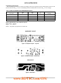
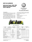
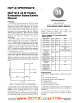
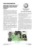
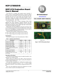
NCP1014STBUCGEVB
Non-isolated Positive
Output Buck AC/DC
Converter Evaluation Board
User's Manual
http://onsemi.com
EVAL BOARD USER’S MANUAL
• Overload, Short−Circuit and Thermal Protected
• Simple for Low Cost Mass Production
• Universal Design for Wide Range of Output Currents
and Voltages
Figure 1. Evaluation Board Photo
The monolithic power switcher, used in this application,
greatly simplifies the total design and reduces time to
production. The new line of the Power Switchers, NCP1010
through NCP1014, is ideal for this purpose. This IC in the
SOT−223 package reduces size and is suitable for mass
production. The design consists of input filter, rectifier with
filtering capacitor, power stage with switcher and inductor,
output ultrafast rectifier, output filtering capacitor, feedback
loop with zener diode and optocoupler and indicating LED.
The only component necessary for proper powering of the
IC is the VCC capacitor. The IC is directly powered from the
HV Drain circuit via internal voltage regulator. To eliminate
the noise at the feedback input, some small ceramic
capacitor with value of around 1.0 nF is necessary to be
connected as close to the FB pin, as possible.
This manual describes the way, how to easily design the
simple, non isolated AC/DC converter for powering low
voltage control part of mains applications with triac, or SCR
power switch. Some examples are: dishwashers, microwave
ovens, coffee machines, night illumination and so on. In
comparison with resistive, or capacitive dropper is this
solution more comfortable and features some advantages
such as:
• Wide Input Voltage Range 85 VAC – 265 VAC
• Smaller Size, Lower Weight, Lower Total Cost
• Good Line and Load Regulation, No Need of
Additional Linear Regulators
• Efficient Design with Up to 80% Efficiency
SCHEMATIC DIAGRAM
E2
220 mF/25 V
C1
100 nF
2
D1
MUR160
E1
+ 10 mF/400 V
1
R1
1k
+
1
2
CON2
ARK750/2
L2
1 mH
+
D2
1N4007
VCC
HV
GND
FB
L1
1.5 mH
CON2
ARK500/2
LD1
GRN
IO2
NCP1014ST
IO1
PC817
E3
47 mF/25 V
ZD1
11 V
C2
1 nF
Figure 2. Complete Schematic Diagram of the 12 V/0.2 A Converter
www.BDTIC.com/ON/
© Semiconductor Components Industries, LLC, 2012
October, 2012 − Rev. 2
1
Publication Order Number:
EVBUM2143/D
NCP1014STBUCGEVB
SELECTION OF CRITICAL COMPONENTS
Inductor selection
The average current through the inductor over one
switching cycle can be expressed by Equation 4.
For the selected output power need to be selected certain
minimum value of the inductance. This value is dependent
on the mode of operation. Reduced value results in
Discontinuous Conduction Mode of operation (DCM).
Practically was found, that the borderline between
Continuous Conduction Mode of operation (CCM) and
DCM is commonly set slightly below maximum output
power. The result is low cost of the inductor, freewheeling
diode (trr > 35 ns), higher efficiency and lower cost. The
negative result is in lower output power and higher cost of
the NCP101x Power Switcher.
The current ripple in the inductor during the Ton time may
be expressed by Equation 1.
DIripple(Ton) + Ton @
Vds * VO)
ǒ(V min *L min
Ǔ
Ic + fop_min @
ǒLVO Ǔ
L min +
Ǔ @ Ton ) ǒ2DI)ripple
Ǔ @ ToffǓ
Iinit
(eq. 4)
(2 @ VO @ IO @ (V min * Vds * VO))
(eq. 5)
(DIripple 2 @ fop_min @ (V min * Vds))
IO = Output DC Current.
The theoretical maximum output power will be shown in
Equation 6.
(eq. 1)
Pout_max + L min @ (Iset 2 * Iinit 2) @ fop_min
@
(V min *Vds)
ǒ(V min
Ǔ
*Vds*VO)
(eq. 6)
2
The current ripple in the inductor during the normal
operation will be shown in Equation 7.
DIripple +
((V min * Vds * VO) @ VO)
(eq. 7)
((V min * Vds) @ fop_min @ L min)
The output current will be shown in Equation 8.
IO + fop_min @
(eq. 2)
min
DIripple
2 ) Iinit
Ic = Inductor Operating Current,
fop_min = Minimum Operating Frequency
The theoretical minimum inductor value corresponds to
Equation 5.
Where:
Ton = ON Time, Internal Power Switch in ON,
Vmin = Minimum Rectified Input Voltage,
Vds = Drain−to−Source Voltage Drop,
Vo = Output Voltage,
Lmin = Minimum Inductor Value.
The current ripple in the inductor during the Toff time may
be expressed by Equation 2.
DIripple(Toff) + Toff @
ǒǒ
((Iset ) Iinit) @ Ton ) (Iset ) Iinit) @ Toff)
(eq. 8)
2
Toff = OFF Time, Internal Power Switch in OFF.
The current through the inductor at the beginning of the
Ton time is shown by Equation 3.
Iinit + Iset * DIripple
(eq. 3)
Iset = Peak Switching Current Set by the FB Loop.
Table 1. TABLE OF PRESELECTED INDUCTORS (Vmin = 120 V, Vds = 9 V, VO = 12 V, Iset = 0.405 A, fop_min = 59 kHz)
NOTE:
Inductance
(mH)
Coilcraft Part Number
(see appendix for address)
DIripple
(A)
Output Current
(A)
470
RFB0810−471
0.39
0.25
680
RFB0810−681
0.27
0.32
820
RFB0810−821
0.22
0.34
1000
RFB0810−102
0.18
0.36
1500
RFB0810−152
0.12
0.40
The output current is the theoretical value and need to be multiplied by the efficiency (~0.7).
www.BDTIC.com/ON/
http://onsemi.com
2
NCP1014STBUCGEVB
Freewheeling diode selection
The freewheeling diode needs to be selected accordingly to the mode of operation. For the CCM operation needs to be used
the ultra fast diode with trr < 35 ns. For the DCM operation the standard ultra fast diode with trr < 75 ns is enough.
Table 2. TABLE OF PRESELECTED FREEWHEELING DIODES
Part number
VRRM
(V)
IF(AV)
(A)
trr
(ns)
Package
MUR160
600
1.0
75
Axial Lead
MURA160T3
600
1.0
75
SMD SMA
MURS160T3
600
1.0
75
SMD SMB
MURS260T3
600
2.0
75
SMD SMB
Electrical Specification of the example at Figure 2:
Input: 85 VAC – 265 VAC
Output: + 12 V / 200 mA
NOTE: The polarity is proportional to common line.
COMPONENT LAYOUT
Figure 3. Component Layout – Top Side
Figure 4. Component Layout – Bottom Side
PCB LAYOUT
Figure 5. PCB Layout
www.BDTIC.com/ON/
http://onsemi.com
3
NCP1014STBUCGEVB
EMI TEST RESULTS
Test Conditions:
Input: 230 VAC
Output: 11.7 VDC
Load: Resistive 68 R
Figure 6. Conducted EMI
TEST PROCEDURE
• 1 DC Volt-Meter able to measure up to 20 V DC (e.g.
Necessary Equipment:
• 1 Current limited 90 − 265 Vrms AC source (current
DC ELECTRONIC
LOAD
+
−
•
• 1 DC Amp-Meter able to measure up to 500 mA DC
•
(e.g. KEITHLEY 2000)
1 DC Electronic Load (e.g. AGILENT 6060B)
V
V
A
A
REGULATED AC
SUPPLY
•
KEITHLEY 2000)
limited to avoid board destruction in case of a defective
part) or a 380 VDC source (e.g. AGILENT 681x)
1 AC Volt-Meter able to measure up to 300 V AC (e.g.
KEITHLEY 2000)
1 AC Amp-Meter able to measure up to 1 A AC (e.g.
KEITHLEY 2000)
Figure 7. Test Setup
• Power down the load
• Power down Uin
• End of test
Test Procedure
•
•
•
•
•
•
Connect the test setup as shown in Figure 7.
Apply an input voltage, Uin = 90 − 265 Vac
Apply Iout(load) = 0 A
Check that Uout is 12 Vdc
Increase Iout(load) load to: 12 V / 200 mA
Check that Uout is 12 V
NOTE: Be careful when manipulating the boards in
operation, lethal voltages up to 265 Vac are
present on the primary side.
www.BDTIC.com/ON/
http://onsemi.com
4
NCP1014STBUCGEVB
BILL OF MATERIAL
Table 3. NCP1014STBUCGEVB EVALUATION BOARD BILL OF MATERIALS
Designator
QTY
Description
Value
Tolerance
C1
1
Capacitor X2
100 nF
C2
1
CMS Capacitor
CON1
1
CON2
Substitution
Allowed
RoHS
Compliant
Footprint
Manufacturer
Manufacturer Part
Number
±10%
Through
Hole
Vishay
F1772−410−2030
Yes
Yes
1 nF
±10%
1206
AVX
12065C102KAT2A
Yes
Yes
Input Terminal
Block
LP7.5/2/903.2
OR
−
LP7.5/2
WeidMuller
LP7.5/2/903.2 OR
Yes
Yes
1
Output Terminal
Block
PM5.08/2/90
−
PM5.08/2
WeidMuller
PM5.08/2/90
Yes
Yes
D1
1
Ultrafast Power
Rectifier
MURA160
−
SMA
ON
Semiconductor
MURA160T3G
No
Yes
D2
1
1 A, 1000 V
Standard Rectifier
1N4007
−
Axial
Lead
ON
Semiconductor
1N4007RLG
No
Yes
E1
1
Electrolytic
Capacitor
10 uF / 400 V
±20%
Through
Hole
Panasonic
ECA2GHG100
Yes
Yes
E2
1
Electrolytic
Capacitor
220 uF / 25 V
±20%
Through
Hole
Panasonic
ECA1EHG221
Yes
Yes
E3
1
Electrolytic
Capacitor
47 uF / 25 V
±20%
Through
Hole
Rubycon
25ML47M6.3X5
Yes
Yes
IO1
1
Opto−Coupler
PC817
−
DIL−4
Sharp
PC817X1J000F
Yes
Yes
IO2
1
Monolithic Power
Switcher
NCP1014
−
SOT−223
ON
Semiconductor
NCP1014ST65T3G
No
Yes
L1
1
Inductor
1.5 mH
±10%
RFB0810
Coil Craft
RFB0810−152
Yes
Yes
L2
1
Inductor
1 mH / 1.6 A
±10%
Through
Hole
Fastron
SMCC−R10X−YY
Yes
Yes
LD1
1
LED
Green LED
5 mm
−
Through
Hole
Avago
HLMP−HM57−SV000
Yes
Yes
R1
1
CMS Resistor
1 kW
±1%
1206
Vishay
RCA12061K00FKEA
Yes
Yes
ZD1
1
Zener Diode
11 V
±5%
SOD−123
ON
Semiconductor
MMSZ11T1G
No
Yes
ON Semiconductor and
are registered trademarks of Semiconductor Components Industries, LLC (SCILLC). SCILLC owns the rights to a number of patents, trademarks,
copyrights, trade secrets, and other intellectual property. A listing of SCILLC’s product/patent coverage may be accessed at www.onsemi.com/site/pdf/Patent−Marking.pdf. SCILLC
reserves the right to make changes without further notice to any products herein. SCILLC makes no warranty, representation or guarantee regarding the suitability of its products for any
particular purpose, nor does SCILLC assume any liability arising out of the application or use of any product or circuit, and specifically disclaims any and all liability, including without
limitation special, consequential or incidental damages. “Typical” parameters which may be provided in SCILLC data sheets and/or specifications can and do vary in different applications
and actual performance may vary over time. All operating parameters, including “Typicals” must be validated for each customer application by customer’s technical experts. SCILLC
does not convey any license under its patent rights nor the rights of others. SCILLC products are not designed, intended, or authorized for use as components in systems intended for
surgical implant into the body, or other applications intended to support or sustain life, or for any other application in which the failure of the SCILLC product could create a situation where
personal injury or death may occur. Should Buyer purchase or use SCILLC products for any such unintended or unauthorized application, Buyer shall indemnify and hold SCILLC and
its officers, employees, subsidiaries, affiliates, and distributors harmless against all claims, costs, damages, and expenses, and reasonable attorney fees arising out of, directly or indirectly,
any claim of personal injury or death associated with such unintended or unauthorized use, even if such claim alleges that SCILLC was negligent regarding the design or manufacture
of the part. SCILLC is an Equal Opportunity/Affirmative Action Employer. This literature is subject to all applicable copyright laws and is not for resale in any manner.
PUBLICATION ORDERING INFORMATION
LITERATURE FULFILLMENT:
Literature Distribution Center for ON Semiconductor
P.O. Box 5163, Denver, Colorado 80217 USA
Phone: 303−675−2175 or 800−344−3860 Toll Free USA/Canada
Fax: 303−675−2176 or 800−344−3867 Toll Free USA/Canada
Email: [email protected]
N. American Technical Support: 800−282−9855 Toll Free
USA/Canada
Europe, Middle East and Africa Technical Support:
Phone: 421 33 790 2910
Japan Customer Focus Center
Phone: 81−3−5817−1050
ON Semiconductor Website: www.onsemi.com
Order Literature: http://www.onsemi.com/orderlit
For additional information, please contact your local
Sales Representative
www.BDTIC.com/ON/
http://onsemi.com
5
EVBUM2143/D