1
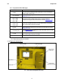
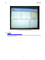
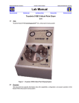
Marvell NanoLab
Member login
Lab Manual Contents
MercuryWeb
Berkeley Microlab
Chapter 8.07
Surface Charge Analyzer
(sca - 386)
1.0
T it le
SCA Operation
2.0
Pu rp ose
The Surface Charge Analyzer (SCA, Model 2500) provides the capability for nondestructive monitoring
of contamination and changes in process conditions on wafer surfaces. It can measure wafers of any
oxide/nitride thickness including bare wafers.
The SCA measurement is an electro-optical extension of C-V method. It works by shining modulated
light on the semiconductor and measuring the resulting AC surface photocurrent. The SCA makes
approximately 800 measurements on one test point.
3.0
Sc ope
The document provides the following information:
► Procedures for running a test.
► Modify measurement settings of a recipe.
► Reviewing, modifying, and exporting test results.
4 .0
Ap p lic ab le Do cu me nts
Revision History
SemiTest SCA-2500 Surface Charge Analyzer User Manual (copies in Office and Laboratory).
5 .0
De f in it ions & Proc es s T er mino log y
The following definitions are used in SCA measurements. The equations used in the calculations are
provided in Chapter 4 of the User Manual.
Qind
An induced charge created by a bias voltage during SCA measurement (unit: q/cm2, where q is
the elementary charge).
Wd
The width of a depletion region caused by the induced charge (unit: μm).
Nsc
The dopant concentration of the wafer being measured (unit: atoms/cm3).
Qox
The charge inside the oxide film, without any contribution from the interface (unit: q/cm2).
Qfb
The charge at flatband voltage (unit: q/cm2).
Dit
The density of interface traps (unit: number-of-traps/cm2/eV).
IQF
Interface Quality Factor used for high quality Si/SiO2 interface when the Dit is below the
detection limit (dimensionless).
Ts
Surface minority carrier lifetime (unit: micro-seconds).
sca
6.0
7.0
Chapter 8.07
Saf ety
6.1
Finger Pinching Hazard: The light shield around the measurement stage will rise/lower
automatically. Do not attempt to adjust/retrieve the test wafer when the shield is activated.
6.2
High Voltage Hazard: The probe may be biased to 2000 VDC. Contact at the probe is prevented
by Mylar insulation and the light shield. Do not touch the probe any time to prevent electric shock
and contamination.
6.3
Ionizing Radiation: The SCA is equipped with a probe discharge ionizer, to minimize static noise
that contains polonium 210. The radiation it produces is lower than The Nuclear Regulatory
Commission (NRC) requirement for hazardous labeling.
S t a t i st ic a l/ P r oce ss D a t a
The statistical/process data of Tystar1&2 and Tylan5&6 are posted on the Microlab Web Page under
General Information/Process Monitor.
8.0
A v a i lab l e P r oc ess es, P r oce ss N o t es
There are five standard recipes. You can over-ride the recipe settings when setting up a test. However,
a super-user password is needed to save the changed settings or write new recipes. The bare wafer
recipes can be used for wafers with hysteresis. Two calibration wafers with 3000A of thermal oxide are
kept in the SCA drawer, which must be kept clean at all times. The Nsc start value is labeled on the
calibration wafer shipping trays. Many other users have written recipes that anyone can use.
9.0
8.1
BARE N NEGATIVE: For use with a bare N-type wafer with negative charges.
8.2
BARE N POSITIVE: For use with a bare N-type wafer with positive charges.
8.3
BARE P NEGATIVE: For use with a bare P-type wafer with negative charges.
8.4
BARE P POSITIVE: For use with a bare P-type wafer with positive charges.
8.5
OXIDE: For use with a wafer with thermally grown oxide/nitride film.
E q u ip me nt O pe rat i on
9.1
Overall Equipment Description
The SCA is a one-piece equipment with the measurement station and the control/data-acquisition
computer integrated together. See Section 11.1 for the front view photograph of the equipment.
A wafer stage is located on the right side of the SCA. On the stage, there are several concentric
grooves for the user to align the wafer to be measured. The SCA can accommodate wafers from
100 to 200 mm (4 to 8 inches) in diameter. The wafer is secured in position during the
measurement by vacuum. Be careful when removing wafer after measurement, since the vacuum
needs time be fully vented.
DO NOT TOUCH THE WAFER STAGE AT ANY TIME! Touching the wafer stage may cause
additional contamination which will cause the probe to degrade. The probes are expensive and
should be kept as clean as possible.
Windows NT is the operation system of the control/data-acquisition computer. The SCA software
is controlled by a drop-down menu or graphic buttons on the display screens. To the right of the
monitor, there is a 3.5” floppy disk drive for data export. To protect the integrity of the computer
system, a password is needed to exit the SCA program to the operation system. Do not try to
access the operation system by using the power switch or the reset button located on the left
lower corner of the equipment. The power switch is used for emergency only.
9.2
Log In the SCA Program
9.2.1
Enable the SCA on the WAND.
-2-
sca
Chapter 8.07
9.3
9.2.2
The SCA displays <User Login Screen>. Enter SCA in both user and password fields,
and then click on the Log In button.
9.2.3
The SCA now displays the <Test Screen> (see Section 11.2). There are a drop down
menu and graphic buttons on the screen. Move the cursor to a button to see its function
description.
Test Setup
9.3.1
Click the rectangular Setup Test button located on the lower right of the screen.
9.3.2
The SCA now displays <Setup Test Screen>.
9.3.3
9.3.4
9.4
9.3.2.1
Double check that the Operation field is MANUAL, and the Operating Mode is
NORMAL. These are the defaults for the SCA without the wafer autoloader
feature.
9.3.2.2
Enter the Lot ID and Cassette fields with the test wafer information. If either
field is blank, the test will not start.
Click the Add button if the lower half of the screen is blank. Click the Edit button if it
shows a row of test setup information. <Edit Test Setup Screen> will pop out. There are
six fields to be filled. Click OK button when done.
9.3.3.1
Slot: Should always be ‘1’. It is the default for the MANUAL mode.
9.3.3.2
WaferID: Default is WAFER, but you can enter your own wafer ID.
9.3.3.3
Recipe: Select a recipe from the drop down menu.
9.3.3.4
Pattern: Select a test pattern from the drop down menu. It can take more than
one minute for one test point.
9.3.3.5
Tox (in Angstroms): Enter the thickness of the oxide film. Incorrect entry of
oxide thickness will result in incorrect calculation results. Enter ‘1’ if using a
bare wafer.
9.3.3.6
Sweep: Users can enter whether to sweep the voltage from inversion to
accumulation, I->A (default) or accumulation to inversion, A -> I.
9.3.3.7
Comment: Enter the additional test wafer information (optional).
After <Edit Test Setup screen> is complete, <Setup Test screen> will be updated to
show the measurement conditions specified by the recipe. The test pattern and the wafer
size will also be shown on the wafer map on the upper left corner of the screen.
Modifying Standard Recipe Settings
The default measurement settings specified in the standard recipes are good for most of the
general tests. It is recommended that you use the default value for the first test on a new type of
wafers. Adjust the parameter settings based on Section 10.0 (Troubleshooting), if the test fails.
The parameters set in the measurement recipe can be override by clicking the “Override Recipe”
square. Then enter the new settings or use the drop down menu.
9.4.1
RI: The refractive index of the film being measured.
9.4.2
Qind: The Induced charge sweep range that is used. Highly charged wafers may require a
higher value.
9.4.3
Type: The expected conductivity type (P or N) of the wafer to be tested.
9.4.4
Nsc Start: The expected Nsc value of the wafer to be tested. If the incorrect value is
entered, the test will take longer to perform.
9.4.5
Res Start: The expected resistivity of the wafer to be tested. If the incorrect value is
entered, the test will take longer to perform. Entering an Nsc value will automatically
calculate the Res Start value, and vice versa.
-3-
sca
Chapter 8.07
9.5
9.6
Running A Test
9.5.1
When all fields are complete on <Setup Test Screen>, click the Start Test button on the
bottom of the screen.
9.5.2
The light shield around the wafer stage will go down. A pop-up window will remind you to
insert the test wafer. Click the OK button when done. The light shield will go up, and the
test will begin.
9.5.3
During the test, <TEST Screen> will update the measurement results as each point is
tested. The status line at the bottom of the screen shows the progress of the test.
9.5.4
When all the test points are complete, the status shows DONE. If a parameter exceeds
the Min/Max limits specified in the recipe, the failure will be indicated by (F) next to the
parameter result.
9.5.5
The light shield will go down. Remove the wafer from the chuck. The vacuum is very
strong, but do not use too much force to remove the wafer from the chuck.
9.5.6
Repeat Sections 9.3 to 9.5 for next test wafer.
Reviewing, Modifying, And Managing Test Results
9.6.1
9.6.2
9.6.3
Reviewing Test Results
9.6.1.1
To review test results, select Review Results, Test Results from the drop
down menu. <Result Summary Screen> will automatically display the most
recent test result.
9.6.1.2
To view a different test, click the Select Test button on the bottom left of the
screen. Highlight the Test ID of the desired test and click OK.
9.6.1.3
To view test results stored in the directory other than the default
(C:\SCAWIN32\TEST INFO), click the Change Directory tab on the top right of
the screen, then navigate through the pop-out windows to the desired directory
or the floppy drive.
Modifying Test Results
9.6.2.1
To adjust the onset on inversion, Click the Zoom Wd tab, and then click on the
Wd (μm) up/down-arrow to change the Wd value of the onset of inversion. As
the value changes, the red cross on the curve will move to the new location.
The onset of inversion point is used to calculate the Nsc.
9.6.2.2
Some of the measurement parameters, e.g. oxide thickness, refractive index,
and etc., can be changed for result re-calculation. To do so, click the Test
Parameters tab, then make changes on <TEST PARAMETERS Screen>.
Click on the Result Summary tab, the results will be re-calculated with the
new measurement parameters.
Managing Test Results
9.6.3.1
Click the Result Management tab to copy, move, delete, and export test
results. Notice that the test results of a test point consist of several files in
various subdirectories.
9.6.3.2
On <Result Management Screen>, highlight the desired tests, then click the
corresponding buttons on the bottom of the screen to copy, move, or delete the
test results to/from a directory or floppy diskette. A 1.44Mb floppy diskette can
hold the results of 20 test points.
9.6.3.3
The Summary function extracts the summary results from selected tests and
exports them to a text file.
-4-
sca
Chapter 8.07
9.6.3.4
The Compress function compresses the entire data structure (files in
subdirectories) associated with the selected tests into one single file. You need
the WinZip utility to open the compressed file.
9.6.3.5
The Batch Print function creates a printout showing the Wd-Qind curves for all
points in all selected tests.
1 0 .0 T ro ub l es ho ot i ng G u id e l in es
10.1 Unusual SCA Curves
Problem
Solution
Curves that do not reach midgap, hence
not Qox and Dit calculated.
Re-measure using a higher value of Qind
Wafers that are always in inversion.
Re-measure using a higher value of Qind
Wafers that are always in accumulation.
Re-measure using a higher value of Qind
Curves that do not reach inversion.
Re-measure using a higher value of Qind
Curves with overshoot in Inversion.
The overshoot does not affect measurement results.
Curves with hysteresis in the depletion
region.
Re-measure using one of the bare wafer recipe
(Sections 8.1-4)
Curves with hysteresis but no results.
Wrong bare wafer recipe used. Re-measure with
correct recipe.
Curve with inversion shifts.
Caused by wafer contamination or probe mal-function.
Re-measure with a clean wafer to find out the cause.
Wafers with P-N junctions near the
surface.
SCA cannot measure this kind of wafers.
Wafers with graded junctions near the
surface.
Re-measure with the highest possible value of Qind
Wafers with Dit below resolution.
Follow Section 9.6.2.2 to change the result calculation
from Dit to IQF for the high-quality interface.
Tests with no curves.
Caused by problematic wafer or probe mal-function.
Re-measure with a clean wafer to find out the cause.
-5-
sca
Chapter 8.07
10.2 Computational Error Messages
Problem
Solution
TYPE?
The SCA could not determine the wafer type (P or N). Re-measure
using a higher value of Qind.
Nsc: No Onset
Re-measure using a higher value of Qind, or set the onset manually
(Section 9.6.2.1).
Qox_inv: N/A
Qox_acc: N/A
Qox_int: N/A
Re-measure using a higher value of Qind, or select a different
measurement segment and recalculate the results (Section 9.6.2.2).
D_Qtotal: N/A
D_Qacc: N/A
D_Qinv: N/A
Caused by a problematic wafer or probe mal-function. Re-measure
with a clean wafer to find out the cause.
Dit: N/A
Select a different measurement segment and recalculate the results
(Section 9.6.2.2).
Dit: Below_Res
Follow Section 9.6.2.2 to change the result calculation from Dit to IQF
for the high-quality interface.
Ts: N/A
Caused by wafer contamination or probe mal-function. Re-measure
with a clean wafer to find out the cause.
No Data
Test was aborted.
10.3 Report other problems on WAND.
1 1 .0 F i gu re s & S c he mat i cs
11.1 Front view photograph of the SCA
-6-
sca
Chapter 8.07
11.2 The Test Screen of the SCA Program
12.0 Ap pe nd ix
PSN111 Cleaning the Model C2B-100 Probe
Be sure not to touch the probe if you are cleaning the probe. Ask a superuser for training on how to
remove probes from the sca.
-7-