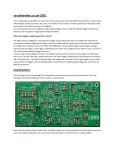
1
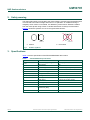
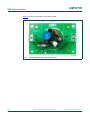
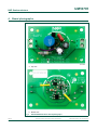
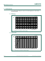
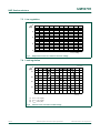
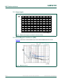
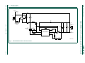
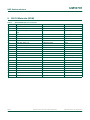
UM10791 SSL5021BDB1205 120 V 6 W candle form non-isolated buck LED driver demo board Rev. 1 — 3 November 2014 User manual Document information Info Content Keywords SSL5021BDB1205, SSL5021BTS, LED driver, non-isolated buck topology, candle applications, TSOP6 package Abstract This user manual describes the performance, technical data, and the connection of the SSL5021BDB1205 demo board, using non-isolated buck topology. The SSL5021BTS is an NXP Semiconductors driver IC in a TSOP6 package. It is intended to provide a low-cost, small form factor LED driver design. This SSL5021BDB1205 demo board is designed for candle-form applications. It operates at 120 V (AC), with an output voltage approximately 54 V. UM10791 NXP Semiconductors SSL5021BDB1205 120 V 6 W candle form buck LED driver demo board Revision history Rev Date Description v.1 20141103 first issue Contact information For more information, please visit: http://www.nxp.com For sales office addresses, please send an email to: [email protected] UM10791 User manual All information provided in this document is subject to legal disclaimers. Rev. 1 — 3 November 2014 © NXP Semiconductors N.V. 2014. All rights reserved. 2 of 18 UM10791 NXP Semiconductors SSL5021BDB1205 120 V 6 W candle form buck LED driver demo board 1. Introduction WARNING Lethal voltage and fire ignition hazard The non-insulated high voltages that are present when operating this product, constitute a risk of electric shock, personal injury, death and/or ignition of fire. This product is intended for evaluation purposes only. It shall be operated in a designated test area by personnel qualified according to local requirements and labor laws to work with non-insulated mains voltages and high-voltage circuits. This product shall never be operated unattended. This user manual describes the operation of the SSL5021BDB1205 demo board featuring LED driver SSL5021BTS in a 120 V/6 W non-isolated application. The SSL5021BDB1205 demo board is designed for driving LED loads from 40 V to 60 V with a nominal value of 55 V. The PCB dimensions are compatible with candle applications. The SSL5021BDB1205 demo board provides a simple and effective solution with a low output current ripple and high efficiency for Solid-State Lighting (SSL) applications. 1.1 Features • • • • • • • UM10791 User manual Candle-form application Open/short LED string protection OverCurrent Protection (OCP) OverTemperature Protection (OTP) Efficiency > 88 % at 120 V (AC) input Compliant with IEC61000-3-2 harmonic standard Compliant with EN55015 conducted EMI All information provided in this document is subject to legal disclaimers. Rev. 1 — 3 November 2014 © NXP Semiconductors N.V. 2014. All rights reserved. 3 of 18 UM10791 NXP Semiconductors SSL5021BDB1205 120 V 6 W candle form buck LED driver demo board 2. Safety warning The demo board input is connected to the mains voltage. Avoid touching the board while it is connected to the mains voltage and when it is in operation. An isolated housing is obligatory when used in uncontrolled, non-laboratory environments. Galvanic isolation from the mains phase using a fixed or variable transformer is always recommended. Figure 1 shows the symbols on how to recognize these devices. 019aab174 019aab173 a. Isolated Fig 1. b. Not isolated Isolation symbols 3. Specifications Table 1 lists the specification of the SSL5021BDB1205 demo board. Table 1. UM10791 User manual SSL5021BDB1205 specifications Symbol Parameter Value Vmains AC mains supply voltage 120 V (AC); 10 % Pout output power 6W VLED output voltage 40 V to 60 V (54 V optimum) ILED output current 93 mA Iripple output current ripple at 120 Hz <3% ILED(Vmains)/ILED(nom) line regulation 1.0 % at Vmains = 90 V to 150 V ILED(VLED)/ILED(nom) load regulation 0.7 % at VLED, 10 % efficiency 89 %; at 120 V (AC)/60 Hz PF power factor >0.55 at 120 V (AC)/60 Hz Toper operating temperature 40 C to +105 C board dimensions 60 mm 40 mm conducted electrostatic Interference (EMI) EN55015 IEC61000-3-2 Class D (for Pin < 25 W limit) All information provided in this document is subject to legal disclaimers. Rev. 1 — 3 November 2014 © NXP Semiconductors N.V. 2014. All rights reserved. 4 of 18 UM10791 NXP Semiconductors SSL5021BDB1205 120 V 6 W candle form buck LED driver demo board Figure 2 shows the dimensions of the demo board. Fig 2. UM10791 User manual SSL5021BDB1205 demo board dimensions All information provided in this document is subject to legal disclaimers. Rev. 1 — 3 November 2014 © NXP Semiconductors N.V. 2014. All rights reserved. 5 of 18 UM10791 NXP Semiconductors SSL5021BDB1205 120 V 6 W candle form buck LED driver demo board 4. Board photographs a. Top view b. Bottom view Fig 3. UM10791 User manual SSL5021BDB1205 demo board photographs All information provided in this document is subject to legal disclaimers. Rev. 1 — 3 November 2014 © NXP Semiconductors N.V. 2014. All rights reserved. 6 of 18 UM10791 NXP Semiconductors SSL5021BDB1205 120 V 6 W candle form buck LED driver demo board 5. Board connections The SSL5021BDB1205 demo board is optimized for a 120 V (AC)/60 Hz supply. It is designed to work with multiple LEDs or an LED module. Under the expected conditions, the output current is 93 mA when using an LED string with a 55 V forward voltage (VF). The current can be adjusted using resistors R5. A 55 V LED voltage gives a good efficiency and line regulation at 120 V (AC). K1 is the connection for the mains voltage. LED+ and LED are the connections for the LED load. Figure 4 shows the connections. Fig 4. SSL5021BDB1205 board connections 6. Functional description 6.1 Input filtering Capacitors C1 and C3 and inductor L1 filter the switching current from the buck converter to the line. Capacitors C1 and C3 also provide a low-impedance path for the switching current. The value of C1 is selected to have no more than 30 % ripple on the bus voltage at 15 % of typical mains. The input series resistance of 10 and capacitor C1 together provide adequate protection against transient surge voltages. A footprint for an optional varistor RV1 is available on the board. To increase the immunity to the line surge, the input resistance is added (see Figure 11). Do not omit this resistor or lower its value. 6.2 Efficiency improvement for universal mains The SSL5021BTS is supplied via start-up resistors R3 and R4. To keep the temperature low and retain ease of adjustment of the desired value, the power losses in these resistors are divided over the two resistors. UM10791 User manual All information provided in this document is subject to legal disclaimers. Rev. 1 — 3 November 2014 © NXP Semiconductors N.V. 2014. All rights reserved. 7 of 18 UM10791 NXP Semiconductors SSL5021BDB1205 120 V 6 W candle form buck LED driver demo board For mains voltages up to 120 V (AC), a single 1206 size SMD resistor (R3) is sufficient. The maximum voltage and the power rating are not exceeded. 6.3 Open-load protection The driver board is protected when the LED load is accidentally left open. The open-load protection is a non-latched protection. Two circuits set the open-load output voltage. One circuit sets the open-load output voltage when the IC does not operate because of a defect. The other circuit sets it when the IC is operating normally. In all cases, the output voltage must never exceed the rated DC voltage of the output capacitor. Do not reconnect the LEDs directly after an open-load situation. The output capacitor is charged to a higher voltage than the total LED voltage, forcing an uncontrolled discharge current through the LEDs when connected. It can damage the LEDs permanently. IC not operating: The voltage divider consisting of resistors R3 and R4 sets the output voltage from the VCC pin of the IC to the GND pin of the IC and resistor R9. V drain – 15 R9 V out = ----------------------------------------- R3 + R4 + R9 (1) n 2.5 V As a rule of thumb, limit resistor R9 to --------------------------- . In this way, the voltage is not sufficient 225 A to illuminate the LEDs (n is the number of LEDs in series at the output. The non-operating output voltage must not be equal to or exceed the voltage set by the operating mode. It is good practice to set the level in non-operating mode 5 V to 10 V lower than in operating mode. IC operating: When the voltage in the non-operating mode is set to a safe level for the output capacitor, the voltage in the operating mode can be set. The DEMOVP pin detects overvoltage. It triggers when 4 consecutive high-frequency cycles at 1.8 V are detected at the DEMOVP R6 + R7 + R8 pin. V out = 1.8 -------------------------------------- sets the output voltage. R6 The output voltage must never exceed the rated DC voltage of the output capacitor. 6.4 External overtemperature protection and LED current foldback Figure 11 shows the footprints of resistors R5 and R6. The purpose of these resistors is to provide thermal protection. To reduce light output when using output current foldback, the DEMOVP pin can be used as an input. Replace resistor R5 by a 470 PTC resistor. Resistor R6 is kept at 5.1 k. If the foldback option is not used, resistor R5 can be shorted and resistor R6 can be set to 5.6 k. When the foldback option is not used, efficiency can be further improved by increasing R6 to 12 k. Do not use a value > 18 k for resistor R6. If the value of resistor R6 is increased too much, the DEMOVP pin can cause false OVP triggering. UM10791 User manual All information provided in this document is subject to legal disclaimers. Rev. 1 — 3 November 2014 © NXP Semiconductors N.V. 2014. All rights reserved. 8 of 18 UM10791 NXP Semiconductors SSL5021BDB1205 120 V 6 W candle form buck LED driver demo board 6.5 LED current and sense resistors To optimally profit from the excellent current stability of the SSL5021BTS, overtemperature 50 ppm MELF type resistors are chosen to sense the LED current. The output current stability range drops to 3 % compared to 7 % over the full temperature range for normal 200 ppm 1206 type resistors. In most low-power, low-cost applications with LED currents < 150 mA, 200 ppm resistors are fine. ILED(AV) = 0.4 / R5 can adjust the average LED current. If the change is small (10 %), changing the inductor is not required. At the lowest mains voltage, the maximum ON-time of Q1 must not exceed 15 s. When the sense resistor is operating at high temperatures, its power rating must be rated by a factor 2. UM10791 User manual All information provided in this document is subject to legal disclaimers. Rev. 1 — 3 November 2014 © NXP Semiconductors N.V. 2014. All rights reserved. 9 of 18 UM10791 NXP Semiconductors SSL5021BDB1205 120 V 6 W candle form buck LED driver demo board 7. Performance Vmains = 85 V to 140 V (AC); tamb = 25 °C; ILED = 93 mA typical; VLED = 55 V unless otherwise specified. 7.1 Efficiency DDD Ș Fig 5. 9PDLQV9506 Efficiency as a function of mains voltage 7.2 Input power DDD 3LQ : Fig 6. UM10791 User manual 9PDLQV9506 Power factor as a function of mains voltage All information provided in this document is subject to legal disclaimers. Rev. 1 — 3 November 2014 © NXP Semiconductors N.V. 2014. All rights reserved. 10 of 18 UM10791 NXP Semiconductors SSL5021BDB1205 120 V 6 W candle form buck LED driver demo board 7.3 Line regulation DDD ,/(' P$ Fig 7. 9PDLQV9506 Output LED current as a function of mains voltage 7.4 Load regulation DDD ,/(' P$ 9/('9 (1) Vmains = 140 V (AC) (2) Vmains = 120 V (AC) (3) Vmains = 85 V (AC) Fig 8. UM10791 User manual LED current as a function of LED voltage All information provided in this document is subject to legal disclaimers. Rev. 1 — 3 November 2014 © NXP Semiconductors N.V. 2014. All rights reserved. 11 of 18 UM10791 NXP Semiconductors SSL5021BDB1205 120 V 6 W candle form buck LED driver demo board 7.5 Output ripple DDD 5LSSOH Fig 9. 9PDLQV9506 Output current ripple as a function of mains voltage 7.6 ElectroMagnetic Interference (EMI) Figure 10 shows the conducted EMI result of the SSL5021BDB1205 demo board. Fig 10. EMI performance UM10791 User manual All information provided in this document is subject to legal disclaimers. Rev. 1 — 3 November 2014 © NXP Semiconductors N.V. 2014. All rights reserved. 12 of 18 xxxxxxxxxxxxxxxxxxxxx xxxxxxxxxxxxxxxxxxxxxxxxxx xxxxxxx x x x xxxxxxxxxxxxxxxxxxxxxxxxxxxxxx xxxxxxxxxxxxxxxxxxx xx xx xxxxx xxxxxxxxxxxxxxxxxxxxxxxxxxx xxxxxxxxxxxxxxxxxxx xxxxxx xxxxxxxxxxxxxxxxxxxxxxxxxxxxxxxxxxx xxxxxxxxxxxx x x xxxxxxxxxxxxxxxxxxxxx xxxxxxxxxxxxxxxxxxxxxxxxxxxxxx xxxxx xxxxxxxxxxxxxxxxxxxxxxxxxxxxxxxxxxxxxxxxxxxxxxxxxx xxxxxxxx xxxxxxxxxxxxxxxxxxxxxxxxx xxxxxxxxxxxxxxxxxxxx xxx NXP Semiconductors UM10791 User manual 8. Schematic ( $:* UHSODFH ZLWKZLUH *1' . & ) 9 5 ȍ :SXOVH ZLWKVWDQGLQJ IXVLVWRU 8 0'6 ' 5 / Nȍ + (6- 5 Nȍ ( $:* & 4 )411& *'6 ' 1:) . 5 ) 9 & ȍ 8 ,616 5 5 Nȍ 9&& ȍ 6: 66/%76 &203 S) 9 / P+ *1' *1'BIORDW & QP ) 9 & Q) 9 /(' /(' &211 ( $:* '(0293 5 Nȍ Fig 11. SSL5021BDB1205 demo board schematic 5 5 Nȍ Nȍ DDD UM10791 13 of 18 © NXP Semiconductors N.V. 2014. All rights reserved. SSL5021BDB1205 120 V 6 W candle form buck LED driver demo board Rev. 1 — 3 November 2014 All information provided in this document is subject to legal disclaimers. PDLQV LQ & Q) 9 UM10791 NXP Semiconductors SSL5021BDB1205 120 V 6 W candle form buck LED driver demo board 9. Bill Of Materials (BOM) Table 2. SSL5021BDB1205 bill of materials Reference Description and values Part number Manufacturer C1 capacitor; 6.8 F; 200 V - Rubycon C3 capacitor; 0.047 F; 400 V CL21-400V-0.047µF-K ZhongShan AIDI Electronics C4 capacitor; 0.22 F; 10 %; 50 V; X7R; 0603 UMK107B7224KA-TR Taiyo Yuden C5 capacitor; 330 pF; 630 V; 0805 C2012C0G2W330J060AA TDK C6 capacitor; 4.7 F; 100 V 100ZLJM Rubycon C9 capacitor; 100 nF; 200 V C1206C104K2RACTU KEMET D1 diode; 100 V; 300 mA 1N4148W-7-F Diodes Incorporated D2 diode; fast; 600 V; 1 A MURS160-E3-52T Vishay K1 terminal block; 2 p.; 5.08 mm 1508060000 Weidmüller K2 terminal block; 2 p.; 5.08 mm 20020109-H021A01LF FCI L1 inductor; 330 H RLB0812-681KL Bourns L2 inductor; 2.2 mH TSL1112RA-222JR33-PF TDK Q1 MOSFET-N; 650 V; 0.8 A FQN1N60C Fairchild R1 resistor; 22 ; 10 %; 2 W; EMC EMC2-22RK Welwyn Components R2 resistor; 220 ; 1 %; 125 mW; 0603 - - R3; R4 resistor; 560 k; 1206 - - R5 resistor; 4.3 ; 1 %; 63 mW; 1206 - - R6 resistor; 5.6 k; 1 %; 63 mW; 0603 - - R7 resistor; 100 k; 1 %; 250 mW; 1206 - - R8 resistor; 100 k; 1 %; 250 mW; 1206 - - R9 resistor; 220 k; 1 %; 250 mW; 1206 - - U1 bridge rectifier; 600 V; 0.8 A B6S-G Comchip Tech U2 IC; SSL5021BTS; TSOP6 SSL5021BTS NXP Semiconductors UM10791 User manual All information provided in this document is subject to legal disclaimers. Rev. 1 — 3 November 2014 © NXP Semiconductors N.V. 2014. All rights reserved. 14 of 18 UM10791 NXP Semiconductors SSL5021BDB1205 120 V 6 W candle form buck LED driver demo board 10. Board layout a. Top view b. Bottom view Fig 12. SSL5021BDB1205 demo board layout UM10791 User manual All information provided in this document is subject to legal disclaimers. Rev. 1 — 3 November 2014 © NXP Semiconductors N.V. 2014. All rights reserved. 15 of 18 UM10791 NXP Semiconductors SSL5021BDB1205 120 V 6 W candle form buck LED driver demo board 11. Abbreviations Table 3. Abbreviations Acronym Description EMI ElectroMagnetic Interference LED Light-Emitting Diode OCP OverCurrent Protection OTP OverTemperature Protection PF Power Factor SSL Solid-State Lighting 12. References [1] UM10791 User manual SSL5021BTS data sheet — Compact low-ripple buck LED driver IC All information provided in this document is subject to legal disclaimers. Rev. 1 — 3 November 2014 © NXP Semiconductors N.V. 2014. All rights reserved. 16 of 18 UM10791 NXP Semiconductors SSL5021BDB1205 120 V 6 W candle form buck LED driver demo board 13. Legal information 13.1 Definitions Draft — The document is a draft version only. The content is still under internal review and subject to formal approval, which may result in modifications or additions. NXP Semiconductors does not give any representations or warranties as to the accuracy or completeness of information included herein and shall have no liability for the consequences of use of such information. NXP Semiconductors does not accept any liability related to any default, damage, costs or problem which is based on any weakness or default in the customer’s applications or products, or the application or use by customer’s third party customer(s). Customer is responsible for doing all necessary testing for the customer’s applications and products using NXP Semiconductors products in order to avoid a default of the applications and the products or of the application or use by customer’s third party customer(s). NXP does not accept any liability in this respect. Export control — This document as well as the item(s) described herein may be subject to export control regulations. Export might require a prior authorization from competent authorities. 13.2 Disclaimers Limited warranty and liability — Information in this document is believed to be accurate and reliable. However, NXP Semiconductors does not give any representations or warranties, expressed or implied, as to the accuracy or completeness of such information and shall have no liability for the consequences of use of such information. NXP Semiconductors takes no responsibility for the content in this document if provided by an information source outside of NXP Semiconductors. In no event shall NXP Semiconductors be liable for any indirect, incidental, punitive, special or consequential damages (including - without limitation - lost profits, lost savings, business interruption, costs related to the removal or replacement of any products or rework charges) whether or not such damages are based on tort (including negligence), warranty, breach of contract or any other legal theory. Notwithstanding any damages that customer might incur for any reason whatsoever, NXP Semiconductors’ aggregate and cumulative liability towards customer for the products described herein shall be limited in accordance with the Terms and conditions of commercial sale of NXP Semiconductors. Right to make changes — NXP Semiconductors reserves the right to make changes to information published in this document, including without limitation specifications and product descriptions, at any time and without notice. This document supersedes and replaces all information supplied prior to the publication hereof. Suitability for use — NXP Semiconductors products are not designed, authorized or warranted to be suitable for use in life support, life-critical or safety-critical systems or equipment, nor in applications where failure or malfunction of an NXP Semiconductors product can reasonably be expected to result in personal injury, death or severe property or environmental damage. NXP Semiconductors and its suppliers accept no liability for inclusion and/or use of NXP Semiconductors products in such equipment or applications and therefore such inclusion and/or use is at the customer’s own risk. Applications — Applications that are described herein for any of these products are for illustrative purposes only. NXP Semiconductors makes no representation or warranty that such applications will be suitable for the specified use without further testing or modification. Customers are responsible for the design and operation of their applications and products using NXP Semiconductors products, and NXP Semiconductors accepts no liability for any assistance with applications or customer product design. It is customer’s sole responsibility to determine whether the NXP Semiconductors product is suitable and fit for the customer’s applications and products planned, as well as for the planned application and use of customer’s third party customer(s). Customers should provide appropriate design and operating safeguards to minimize the risks associated with their applications and products. Evaluation products — This product is provided on an “as is” and “with all faults” basis for evaluation purposes only. NXP Semiconductors, its affiliates and their suppliers expressly disclaim all warranties, whether express, implied or statutory, including but not limited to the implied warranties of non-infringement, merchantability and fitness for a particular purpose. The entire risk as to the quality, or arising out of the use or performance, of this product remains with customer. In no event shall NXP Semiconductors, its affiliates or their suppliers be liable to customer for any special, indirect, consequential, punitive or incidental damages (including without limitation damages for loss of business, business interruption, loss of use, loss of data or information, and the like) arising out the use of or inability to use the product, whether or not based on tort (including negligence), strict liability, breach of contract, breach of warranty or any other theory, even if advised of the possibility of such damages. Notwithstanding any damages that customer might incur for any reason whatsoever (including without limitation, all damages referenced above and all direct or general damages), the entire liability of NXP Semiconductors, its affiliates and their suppliers and customer’s exclusive remedy for all of the foregoing shall be limited to actual damages incurred by customer based on reasonable reliance up to the greater of the amount actually paid by customer for the product or five dollars (US$5.00). The foregoing limitations, exclusions and disclaimers shall apply to the maximum extent permitted by applicable law, even if any remedy fails of its essential purpose. Safety of high-voltage evaluation products — The non-insulated high voltages that are present when operating this product, constitute a risk of electric shock, personal injury, death and/or ignition of fire. This product is intended for evaluation purposes only. It shall be operated in a designated test area by personnel that is qualified according to local requirements and labor laws to work with non-insulated mains voltages and high-voltage circuits. The product does not comply with IEC 60950 based national or regional safety standards. NXP Semiconductors does not accept any liability for damages incurred due to inappropriate use of this product or related to non-insulated high voltages. Any use of this product is at customer’s own risk and liability. The customer shall fully indemnify and hold harmless NXP Semiconductors from any liability, damages and claims resulting from the use of the product. Translations — A non-English (translated) version of a document is for reference only. The English version shall prevail in case of any discrepancy between the translated and English versions. 13.3 Trademarks Notice: All referenced brands, product names, service names and trademarks are the property of their respective owners. GreenChip — is a trademark of NXP Semiconductors N.V. UM10791 User manual All information provided in this document is subject to legal disclaimers. Rev. 1 — 3 November 2014 © NXP Semiconductors N.V. 2014. All rights reserved. 17 of 18 UM10791 NXP Semiconductors SSL5021BDB1205 120 V 6 W candle form buck LED driver demo board 14. Contents 1 1.1 2 3 4 5 6 6.1 6.2 6.3 6.4 6.5 7 7.1 7.2 7.3 7.4 7.5 7.6 8 9 10 11 12 13 13.1 13.2 13.3 14 Introduction . . . . . . . . . . . . . . . . . . . . . . . . . . . . 3 Features . . . . . . . . . . . . . . . . . . . . . . . . . . . . . . 3 Safety warning . . . . . . . . . . . . . . . . . . . . . . . . . . 4 Specifications. . . . . . . . . . . . . . . . . . . . . . . . . . . 4 Board photographs . . . . . . . . . . . . . . . . . . . . . . 6 Board connections . . . . . . . . . . . . . . . . . . . . . . 7 Functional description . . . . . . . . . . . . . . . . . . . 7 Input filtering . . . . . . . . . . . . . . . . . . . . . . . . . . . 7 Efficiency improvement for universal mains . . . 7 Open-load protection . . . . . . . . . . . . . . . . . . . . 8 External overtemperature protection and LED current foldback . . . . . . . . . . . . . . . . . . . . . . . . 8 LED current and sense resistors . . . . . . . . . . . 9 Performance . . . . . . . . . . . . . . . . . . . . . . . . . . . 10 Efficiency . . . . . . . . . . . . . . . . . . . . . . . . . . . . 10 Input power . . . . . . . . . . . . . . . . . . . . . . . . . . . 10 Line regulation . . . . . . . . . . . . . . . . . . . . . . . . 11 Load regulation . . . . . . . . . . . . . . . . . . . . . . . . 11 Output ripple . . . . . . . . . . . . . . . . . . . . . . . . . . 12 ElectroMagnetic Interference (EMI) . . . . . . . . 12 Schematic . . . . . . . . . . . . . . . . . . . . . . . . . . . . . 13 Bill Of Materials (BOM) . . . . . . . . . . . . . . . . . . 14 Board layout . . . . . . . . . . . . . . . . . . . . . . . . . . . 15 Abbreviations . . . . . . . . . . . . . . . . . . . . . . . . . . 16 References . . . . . . . . . . . . . . . . . . . . . . . . . . . . 16 Legal information. . . . . . . . . . . . . . . . . . . . . . . 17 Definitions . . . . . . . . . . . . . . . . . . . . . . . . . . . . 17 Disclaimers . . . . . . . . . . . . . . . . . . . . . . . . . . . 17 Trademarks. . . . . . . . . . . . . . . . . . . . . . . . . . . 17 Contents . . . . . . . . . . . . . . . . . . . . . . . . . . . . . . 18 Please be aware that important notices concerning this document and the product(s) described herein, have been included in section ‘Legal information’. © NXP Semiconductors N.V. 2014. All rights reserved. For more information, please visit: http://www.nxp.com For sales office addresses, please send an email to: [email protected] Date of release: 3 November 2014 Document identifier: UM10791 Mouser Electronics Authorized Distributor Click to View Pricing, Inventory, Delivery & Lifecycle Information: NXP: SSL5021BDB1205UL