1
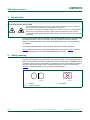
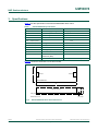
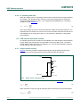
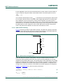
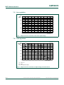
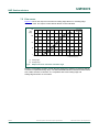
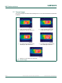
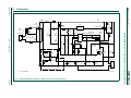
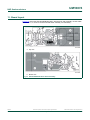
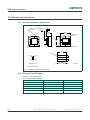
UM10874 SSL5231BDB1289 120 V 18 W dimmable buck non-isolated LED driver Rev. 1 — 23 April 2015 User manual Document information Info Content Keywords SSL5231BDB1289, SSL5231BT, dimmable, LED driver, buck converter, fixture, eco-THD Abstract This user manual describes the operation of the SSL5231BDB1289 120 V 18 W eco-THD dimmable LED driver featuring the SSL5231BT. The SSL5231BDB1289 demo board uses a buck topology. UM10874 NXP Semiconductors SSL5231BDB1289 120 V 18 W dimmable buck non-isolated LED driver Revision history Rev Date Description v.1 20150423 first issue Contact information For more information, please visit: http://www.nxp.com For sales office addresses, please send an email to: [email protected] UM10874 User manual All information provided in this document is subject to legal disclaimers. Rev. 1 — 23 April 2015 © NXP Semiconductors N.V. 2015. All rights reserved. 2 of 25 UM10874 NXP Semiconductors SSL5231BDB1289 120 V 18 W dimmable buck non-isolated LED driver 1. Introduction WARNING Lethal voltage and fire ignition hazard The non-insulated high voltages that are present when operating this product, constitute a risk of electric shock, personal injury, death and/or ignition of fire. This product is intended for evaluation purposes only. It shall be operated in a designated test area by personnel qualified according to local requirements and labor laws to work with non-insulated mains voltages and high-voltage circuits. This product shall never be operated unattended. This user manual describes the operation of the SSL5231BDB1289 120 V 18 W eco-THD dimmable LED driver. The buck converter topology provides a simple and efficient solution for mains dimmable LED recessed light applications with a very good dimmer compatibility. The SSL5231BDB1289 demo board complies with EMI and safety regulations. Figure 2 shows dimensions of the SSL5231BDB1289 demo board. Figure 3 shows the top view and bottom view of the SSL5231BDB1289 demo board. 2. Safety warning The demo board input is connected to the 120 V mains supply. Avoid touching the board while it is connected to the mains voltage and when it is in operation. An isolated housing is obligatory when used in uncontrolled, non-laboratory environments. Galvanic isolation from the mains phase using a fixed or variable transformer is always recommended. Figure 1 shows the symbols on how to recognize these devices. 019aab174 019aab173 a. Isolated Fig 1. UM10874 User manual b. Not isolated Isolation symbols All information provided in this document is subject to legal disclaimers. Rev. 1 — 23 April 2015 © NXP Semiconductors N.V. 2015. All rights reserved. 3 of 25 UM10874 NXP Semiconductors SSL5231BDB1289 120 V 18 W dimmable buck non-isolated LED driver 3. Specifications Table 1 lists the specification of the SSL5231BDB1289 demo board. Table 1. SSL5231BDB1289 specifications Symbol Parameter Value Vmains AC mains supply voltage 120 V (AC); 10 % Imains AC mains input current 150 mA; 5 % VLED output voltage 48 V; 10 % ILED output current 325 mA ILED/ILED(nom)Vmains line regulation > 3 % at Vmains 10 % ILED/ILED(nom)VLED load regulation > 3 % at VLED; 10 % efficiency > 87 % PF power factor > 0.95 Toper operating temperature 40 C to +85 C - board dimensions 30 mm 85 mm - conducted ElectroMagnetic Interference (EMI) FCC15 class B - IEC61000-3-2 class C (for Pin < 25 W limit) Figure 2 shows the dimensions of the demo board. PDLQVLQ /('RXW 66/%'% FRPSRQHQWVLGHDUHD 3&% VROGHULQJVPGVLGHDUHD 'LPHQVLRQVLQPP Fig 2. UM10874 User manual DDD SSL5231BDB1289 demo board dimensions All information provided in this document is subject to legal disclaimers. Rev. 1 — 23 April 2015 © NXP Semiconductors N.V. 2015. All rights reserved. 4 of 25 UM10874 NXP Semiconductors SSL5231BDB1289 120 V 18 W dimmable buck non-isolated LED driver 4. Board photographs a. Top view b. Bottom view Fig 3. UM10874 User manual SSL5231BDB1289 demo board photographs All information provided in this document is subject to legal disclaimers. Rev. 1 — 23 April 2015 © NXP Semiconductors N.V. 2015. All rights reserved. 5 of 25 UM10874 NXP Semiconductors SSL5231BDB1289 120 V 18 W dimmable buck non-isolated LED driver 5. Board connections The SSL5231BDB1289 demo board is optimized for a 120 V/60 Hz supply. In addition to the mains voltage optimization, the board is designed to work with multiple LEDs or an LED module with a low forward voltage. The mains connection of the SSL5231BDB1289 demo board is different from other demo boards. Connect the mains to the screw connector X1. Remark: The maximum rated voltage of the board is 150 V (AC). The anode of the LED load is connected to pin 1 of connector X2. The cathode is connected to pin 2 of connector X2. Use an LED string with a typical forward voltage of 48 V/10 % on the SSL5231BDB1289 demo board. Under the expected conditions, the output current is 325 mA when no dimmer is used. It is possible to shorten the board by mounting C8 and C9 upright. Connector X2 can be mounted at a different position. The board becomes 10 mm shorter. If the board is shortened, wire bridge WB1 must be placed. Fig 4. UM10874 User manual SSL5231BDB1289 board connections All information provided in this document is subject to legal disclaimers. Rev. 1 — 23 April 2015 © NXP Semiconductors N.V. 2015. All rights reserved. 6 of 25 UM10874 NXP Semiconductors SSL5231BDB1289 120 V 18 W dimmable buck non-isolated LED driver 6. Functional description and options 6.1 Input filtering Capacitors C1 and C2 and inductors L1 and L3 filter the switching current from the buck converter to the line. Capacitors C1 and C2 also provide a low-impedance path for the switching current. The value of capacitor C2 is selected so the application passes for both conducted and radiated EMI. The 10 input series resistance together with varistor MOV1 across the AC bridge rectifier input provides protection against transient surge voltages. To increase the immunity to line surges, the input resistance is added. Do not omit this resistor. To improve dimming performance, an extra notch filter, inductor L3, capacitor C11, and resistor R2 is added to the input. The extra filter suppresses the common-mode disturbance in the 200 kHz to 300 kHz range. Furthermore, inductor L3 reduces the repetitive inrush current to maximum 2.3 A. The notch filter isolates capacitor C1 from the dimmer, improving the dimming performance. 6.2 Open-load protection The driver board is protected when the LED load is accidentally left open. The open-load protection is a non-latched protection. It recovers when the LED string is reconnected. The LED current is not controlled when reconnecting which can destroy the LED string. So turn off the mains before reconnecting the LED load. Two circuits set the open-load output voltage. One circuit sets the open output voltage when the IC does not operate because of a defect. The other circuit (OVP) sets it when the IC is operating normally. In all cases, the output voltage must never exceed the rated DC voltage of the output capacitor. 6.2.1 IC not operating The voltage divider, consisting of resistors R19 and R20, sets the output voltage from the VCC pin of the IC to the GND pin of the IC and resistor R10. R10 V o = V bus – V CC -----------------------------------------R10 + R19 + R20 (1) n 2.5 V As a rule of thumb, limit resistor R10 to ---------------------------- . 2 190 A In this way, the voltage is not sufficient to turn on the LEDs (n is the number of LEDs in series at the output). Resistor R10 has a double function. It also supplies the dimmer reset circuit. If this circuit is not used, resistor R10 must be connected to GND. The extra offset of 1.2 V caused by Vbe of transistor Q4 and resistor R6 can be neglected in the calculation. The non-operating output voltage must not be equal to or exceed the voltage set by the operating mode. It is good practice to set the level in non-operating mode 5 V to 10 V lower than in operating mode. UM10874 User manual All information provided in this document is subject to legal disclaimers. Rev. 1 — 23 April 2015 © NXP Semiconductors N.V. 2015. All rights reserved. 7 of 25 UM10874 NXP Semiconductors SSL5231BDB1289 120 V 18 W dimmable buck non-isolated LED driver 6.2.2 IC operating with OVP When the voltage in the non-operating mode is set to a safe level for the output capacitor, the voltage in the operating mode can be set. The OVP is triggered when during four consecutive high-frequency cycles, 1.8 V is detected at the DEMOVP pin. The output voltage is set with Equation 2: R18 V o = 1.8 1 + ---------- R17 (2) The output voltage must never exceed the rated DC voltage of the output capacitor. The preferred value for resistor R17 is 5.6 k. Do not use a resistor value that exceeds 18 k. The DEMOVP pin is a high-ohmic input, so it is sensitive to disturbance causing false OVP triggering. 6.3 LED current and sense resistor To optimally profit from the excellent current stability of the SSL5231BT overtemperature, 50 ppm MELF type resistors are recommended to sense the LED current. The output current stability range drops to 3 % compared to 7 % over the full temperature range for normal 200 ppm 1210 type resistors. 6.3.1 Single resistor sensing Figure 5 shows the principle of single resistor sensing. Single resistor sensing is the traditional way of sensing the peak current through the switch and inductor. 9EXV 6(16( 5,616 *1',& / ' /(' *1'UHWXUQ DDD Fig 5. Single resistor sensing principle The LED current for single resistor sensing is calculated with Equation 3: 0.31 I LED = ------------R ISNS (3) When a dimmer is used, the typical maximum peak current that can be reached equals: 1.8 I peak max = ------------R ISNS UM10874 User manual (4) All information provided in this document is subject to legal disclaimers. Rev. 1 — 23 April 2015 © NXP Semiconductors N.V. 2015. All rights reserved. 8 of 25 UM10874 NXP Semiconductors SSL5231BDB1289 120 V 18 W dimmable buck non-isolated LED driver For this application, the LED current amounts 325 mA, which means a sense resistor of 0.9 is required. Using this resistor value would result in a maximum peak current of 1.8 V -------------- = 2.0 A . 0.9 The maximum allowed input current II(SW) = 2 A limits the current through the switch of the IC. The peak current for the IC is too high. It also implies that inductor L2 must be used with a saturation current of at least 2 A. During normal operation, the peak current is approximately 4 times the average LED current (1.3 A). So an inductor saturation current of maximum 1.5 A is sufficient. To meet the requirements to lower the peak IC current and. the peak inductor current, split sense can be used. Split sense uses the existing head room in the peak current detection to lower the IC and inductor current. 6.3.2 Split resistor sensing Figure 6 shows the principle of split resistor sensing. The peak of the primary stroke the inductor current flows through both sense resistors and during the secondary stroke the inductor current only flows through the secondary sense resistor. 9EXV 6(16( 5,616SUL 5,616VHF *1',& / ' /(' *1'UHWXUQ DDD Fig 6. Split resistor sensing principle When the split sense resistor configuration is set up to make maximum use of the overcurrent sense protection head room of the buck converter application, the IC still regulates to the average LED current. The average LED current measured by the voltage between the ISNS pin and the GND pin of the IC divided by the RISNS resistor. When the application is dimmed the converter shifts to peak current regulation. To regulate to the average LED current, the maximum achievable line and load regulation are maintained. Equation 5 to Equation 8 for a buck converter can be used: UM10874 User manual V ocp -------------------------------- = R ISNS pri + R ISNS sec + R bond = R ISNS tot I peak inductor (5) 0.31 R ISNS AV = --------------------I LED AV (6) All information provided in this document is subject to legal disclaimers. Rev. 1 — 23 April 2015 © NXP Semiconductors N.V. 2015. All rights reserved. 9 of 25 UM10874 NXP Semiconductors SSL5231BDB1289 120 V 18 W dimmable buck non-isolated LED driver R ISNS AV = R ISNS sec + R ISNS pri + R bond (7) V LEDP = ---------------V bus (8) Where: • Rbond is the bond wire resistance on the ISNS pin inside the IC • Ipeak(inductor) can be calculated with the SSL5231BT calculation tool • Vocp can be found in the SSL5231BT data sheet. It is 1.8 V typical for the SSL5231BT For a first set-up, assume: • Ipeak(inductor) 4 ILED(AV) • Rbond = 92 To have some margin, Ipeak(inductor) must be 1.8 A. If Ipeak(inductor) exceeds 1.8 A, the IC already moves to peak current regulation during typical operation. Based on Equation 5 to Equation 8, the following can be concluded: R ISNS AV – R ISNS tot R ISNS pri = ----------------------------------------------------- – R bond – 1 (9) R ISNS sec = R ISNS tot – R ISNS pri – R bond (10) The extra advantage of the split sense configuration is that it improves the THD. The peak current drawn from the mains is shifted towards the middle of the half-mains period. The disadvantage of using the split sense configuration in a buck converter is obvious. The bus voltage and the LED voltage determine the duty cycle. So the line regulation and load regulation is worse than for a single sense resistor application. The line regulation and load regulation are not affected in a buck boost converter application that uses split sense. For the SSL5231BDB1289 demo board, the maximum peak current is limited to Ipeak(reg) = 1.33 A, according to: V I max ISNS I peak reg = ------------------------------------------------------R ISNS pri + R ISNS sec UM10874 User manual All information provided in this document is subject to legal disclaimers. Rev. 1 — 23 April 2015 (11) © NXP Semiconductors N.V. 2015. All rights reserved. 10 of 25 UM10874 NXP Semiconductors SSL5231BDB1289 120 V 18 W dimmable buck non-isolated LED driver 6.4 Dimmer zero level restore circuit When the rectified AC line voltage drops to below the LED voltage, a buck converter-based application stops switching. The impedance towards the mains becomes high ohmic. To suppress peak voltages, most dimmers incorporate a filter capacitor in parallel to the switching device. Because the buck converter becomes high ohmic, this capacitor is not discharged properly. It remains charged to the LED voltage. If this capacitor is not discharged properly, deep dimming is hampered. The dimmer may not have a stable and small phase cut. To overcome this problem, the circuit around transistor Q4 builds a discharge circuit or zero level restore circuit. It is not a bleeder circuit as it does not maintain the dimmer hold current. Transistor Q4 is set to conduct a maximum current of 20 mA. This current is set with: V be Q2 + V R5 I C Q4 = --------------------------------R6 (12) The Vbe voltage of transistor Q2 + the voltage across R5 is 0.6 V typical. Transistor Q2 regulates the current of transistor Q4. R5 When the voltage on Vrect exceeds VLED, in this case 50 V, the voltage divider -------------------R4 + R5 turns off transistor Q4. So transistor Q4 does not overheat and no efficiency decrease occurs. Capacitor C4 is used to reduce the control bandwidth. So transistor Q4 does not oscillate at a high frequency, improving the conducted EMI significantly. Resistor R10 supplies the zero restore circuit is supplied from the LED voltage. When the zero level restore circuit is not used, resistor R10 must be connected to GND. UM10874 User manual All information provided in this document is subject to legal disclaimers. Rev. 1 — 23 April 2015 © NXP Semiconductors N.V. 2015. All rights reserved. 11 of 25 UM10874 NXP Semiconductors SSL5231BDB1289 120 V 18 W dimmable buck non-isolated LED driver 7. Performance The performance was measured using an LED load with a 48 V forward at a 440 mA LED output current. Figure 7 to Figure 12 show the performance data. 7.1 Efficiency DDD Ș Fig 7. 9PDLQV9 Efficiency as a function of AC mains input voltage 7.2 Power Factor DDD 3) Fig 8. UM10874 User manual 9PDLQV9 Power factor as a function of AC mains input voltage All information provided in this document is subject to legal disclaimers. Rev. 1 — 23 April 2015 © NXP Semiconductors N.V. 2015. All rights reserved. 12 of 25 UM10874 NXP Semiconductors SSL5231BDB1289 120 V 18 W dimmable buck non-isolated LED driver 7.3 Line regulation DDD ,/(' P$ Fig 9. 9PDLQV9 Output current as a function of AC mains input voltage 7.4 Load regulation DDD /('FXUUHQW P$ /('YROWDJH9 (1) 138 Vmains (2) 120 V (3) 96 V (dimmed output) Fig 10. Output current as a function of output voltage at nominal mains UM10874 User manual All information provided in this document is subject to legal disclaimers. Rev. 1 — 23 April 2015 © NXP Semiconductors N.V. 2015. All rights reserved. 13 of 25 UM10874 NXP Semiconductors SSL5231BDB1289 120 V 18 W dimmable buck non-isolated LED driver 7.5 Dim curves Figure 11 shows the output current when a leading-edge dimmer or a trailing-edge dimmer is used. The output current without dimmer is also indicated. DDD ,/(' P$ QRGLPPHU &RQGXFWLRQDQJOH (1) Trailing-edge (2) Leading-edge Fig 11. Output current as a function of dimmer angle Dimming compatibility includes smooth dimming without any flashing or flickering effects across the complete dimming range. The SSL5231BDB1289 demo board has been tested with a wide selection of dimmers. It is compatible with most leading-edge and trailing-edge dimmers on the market. UM10874 User manual All information provided in this document is subject to legal disclaimers. Rev. 1 — 23 April 2015 © NXP Semiconductors N.V. 2015. All rights reserved. 14 of 25 UM10874 NXP Semiconductors SSL5231BDB1289 120 V 18 W dimmable buck non-isolated LED driver 7.6 ElectroMagnetic Interference (EMI) The ElectroMagnetic Interference (EMI) was measured according to the FCC15 class B standard. The board complies with the requirements. Figure 12 shows the measurement results. a. AC mains (Live) b. AC mains (Neutral) Fig 12. Conducted EMI performance UM10874 User manual All information provided in this document is subject to legal disclaimers. Rev. 1 — 23 April 2015 © NXP Semiconductors N.V. 2015. All rights reserved. 15 of 25 UM10874 NXP Semiconductors SSL5231BDB1289 120 V 18 W dimmable buck non-isolated LED driver 7.7 Thermal images The thermal images are taken after a settling time of 1 hour and in dimmed and undimmed conditions. a. 18 W no dimming top view; Hottest spot: The buck inductor L2 b. 18 W no dimming bottom view; Hottest spot: the SSL5231BT c. 90 leading-edge dimmed top view; Hottest spot: Latch resistor R7 d. 90 leading-edge dimmed bottom view; Hottest spot: Diode D2 e. Dimming to 15 W; Hottest spot: Diode D2 Fig 13. Thermal images UM10874 User manual All information provided in this document is subject to legal disclaimers. Rev. 1 — 23 April 2015 © NXP Semiconductors N.V. 2015. All rights reserved. 16 of 25 UM10874 NXP Semiconductors SSL5231BDB1289 120 V 18 W dimmable buck non-isolated LED driver 8. Protections The IC incorporates the following protections: • • • • • • UnderVoltage Lockout (UVLO) Cycle-by-cycle OverCurrent Protection (OCP) Internal OverTemperature Protection (OTP) Cycle-by-cycle maximum on-time protection Output OverVoltage Protection (OVP) Output Short Protection (OSP) For more detailed information about the IC protections, see the SSL5231BT data sheet (Ref. 1). UM10874 User manual All information provided in this document is subject to legal disclaimers. Rev. 1 — 23 April 2015 © NXP Semiconductors N.V. 2015. All rights reserved. 17 of 25 xxxxxxxxxxxxxxxxxxxxx xxxxxxxxxxxxxxxxxxxxxxxxxx xxxxxxx x x x xxxxxxxxxxxxxxxxxxxxxxxxxxxxxx xxxxxxxxxxxxxxxxxxx xx xx xxxxx xxxxxxxxxxxxxxxxxxxxxxxxxxx xxxxxxxxxxxxxxxxxxx xxxxxx xxxxxxxxxxxxxxxxxxxxxxxxxxxxxxxxxxx xxxxxxxxxxxx x x xxxxxxxxxxxxxxxxxxxxx xxxxxxxxxxxxxxxxxxxxxxxxxxxxxx xxxxx xxxxxxxxxxxxxxxxxxxxxxxxxxxxxxxxxxxxxxxxxxxxxxxxxx xxxxxxxx xxxxxxxxxxxxxxxxxxxxxxxxx xxxxxxxxxxxxxxxxxxxx xxx NXP Semiconductors UM10874 User manual 9. Schematic 95(&7 ' 6* / / 9EXV P+ 5 %' 0'6 ' 5 3(6'9/%$ 0ȍ & ) 9 & / & Q) 9 S) 9 & Q) 9 59 9'56+%6( 1: 8 ',0 &203 9&& 5 ,616 5 & ) 9 ȍ : 5 Nȍ 5 ȍ ,& WKLVMXQFWLRQ '(0293 FORVHWRSLQ 5 6: 5 Nȍ Nȍ *1' QF FORVH WRSLQ FORVH WRSLQ 5 Nȍ 9/('3 & S) 9 5 ȍ 5 Nȍ 5 4 .63$ & Q) 9 5 ȍ Nȍ & S) 9 5 ȍ & Q) 9 4 %&% 5 ȍ / ) GLPPHU]HUROHYHOUHVWRUHUHTXLUHG IRUGHHSGLPDQGQR/)IOLFNHU QP QRWPRXQWHG Fig 14. SSL5231BDB1289 minimum component count schematic diagram ' %=;& QP & ) 9 :% QP ' 0856 & ) 9 9/(' 9 DDD UM10874 18 of 25 © NXP Semiconductors N.V. 2015. All rights reserved. *1' & Q) 9 ; 0.'6 5 Nȍ & Q) 9 SSL5231BDB1289 120 V 18 W dimmable buck non-isolated LED driver Rev. 1 — 23 April 2015 All information provided in this document is subject to legal disclaimers. ; 0.'6 1 5 4 63'1& ȍ ' P+ 9 ) $& $7 5 Nȍ 5 UM10874 NXP Semiconductors SSL5231BDB1289 120 V 18 W dimmable buck non-isolated LED driver 10. Bill Of Materials (BOM) Table 2. SSL5231BDB1289 demo board full BOM Reference Description and values Part number BD1 bridge rectifier; 1 kV; 500 mA MD5S Rectron C1 capacitor; 22 nF; 5 %; 400 V; PET; THT ECQE4223JF Panasonic C2 capacitor; 220 nF; 5 %; 450 V; PET; THT ECWF2W224JAQ Panasonic C3 capacitor; 330 nF; 10 %; 450 V; PET; THT ECWFD2W334KQ Panasonic - Manufacturer C4 capacitor; 2.2 nF; 10 %; 50 V; X7R; 0603 C5 capacitor; 2.2 F; 10 %; 6.3 V; X7R; 0603 C1608X7R0J225K080AB TDK C6 capacitor; 4.7 F; 10 %; 25 V; X7R; 0805 TDK C7 capacitor; 150 nF; 10 %; 50 V; X7R; 0603 - - C8; C9 capacitor; mount horizontal; 330 F; 20 %; 63 V; ALU; THT UPW1J331MHD Nichicon C10 capacitor; 68 pF; 1 %; 500 V; C0G; 0805 CBR08C680FCGAC KEMET C11; C13 capacitor; 220 pF; 5 %; 500 V; C0G; 1206 12067A221JAT2A AVX C12 capacitor; 3.3 nF; 10 %; 100 V; X7R; 0603 - - D1 diode; 280 V; 1 A S1G-E3/61T Vishay D2 diode; TVS; 15 V PESD15VL1BA NXP Semiconductors D3 diode; 600 V; 1 A MURS160-E3-52T Vishay D4 diode; 100 V; 300 mA 1N4148W-7-F Diode Inc. D5 diode; zener; 68 V; 300 mA BZX384-C68 NXP Semiconductors F1 fuse; slow-blow; 1 A MST 1A 250V Multicomp L1 inductor; mount horizontal; 3.3 mH; 280 mA 744772332 Würth Elektronik L2 transformer; 350 H; 5 % 750341594 Würth Elektronik L3 inductor; 3.3 mH; 190 mA 13R335C Murata Q1 MOSFET-N; 650 V; 1.8 A SPD02N60C3 Infineon C2012X7R1E475K125AB - Q2 transistor; NPN; 45 V; 100 mA BC847B NXP Semiconductors Q4 transistor; NPN; 400 V; 300 mA KSPA44TA Fairchild R1 resistor; 10 ; 10 %; 2 W; THT EMC2-10RK Welwyn Components R2 resistor; 560 ; 5 %; 250 mW; 1206 - - R4 resistor; 820 k; 1 %; 250 mW; 1206 - - R5 resistor; 10 k; 1 %; 63 mW; 0603 - - R6 resistor; 33 ; 1 %; 250 mW; 1206 - - R7 resistor; 470 ; 5 %; 2 W; THT ROX2SJ470R TE Connectivity R8 resistor; 750 k; 1 %; 250 mW; 1206 - - R9 resistor; 27 k; 1 %; 63 mW; 0603 - - R10 resistor; 39 k; 1 %; 250 mW; 1206 - - R11 resistor; 1.3 M; 1 %; 63 mW; 0603 - - R12; R13; R14; R15 resistor; 1.3 ; 1 %; 250 mW; 1206 - - R16 resistor; 220 ; 1 %; 63 mW; 0603 - - UM10874 User manual All information provided in this document is subject to legal disclaimers. Rev. 1 — 23 April 2015 © NXP Semiconductors N.V. 2015. All rights reserved. 19 of 25 UM10874 NXP Semiconductors SSL5231BDB1289 120 V 18 W dimmable buck non-isolated LED driver Table 2. SSL5231BDB1289 demo board full BOM …continued Reference Description and values Part number Manufacturer R17 resistor; 5.6 k; 1 %; 63 mW; 0603 - - R18; R19 resistor; 180 k; 1 %; 250 mW; 1206 - - R20 resistor; 4.7 k; 1 %; 250 mW; 1206 - - RV1 resistor; VDR; 150 V; 20 J VDRS07H150BSE Vishay U1 dimmable LED Driver; SSL5231BT SSL5231BT NXP Semiconductors WB1 wire bridge; 0.8 mm; P = 5.08 mm 923345-02 3M X1; X2 connector; terminal block; 5.00 mm 1715022 Phoenix Contact UM10874 User manual All information provided in this document is subject to legal disclaimers. Rev. 1 — 23 April 2015 © NXP Semiconductors N.V. 2015. All rights reserved. 20 of 25 UM10874 NXP Semiconductors SSL5231BDB1289 120 V 18 W dimmable buck non-isolated LED driver 11. Board layout Figure 15 shows the SSL5231BDB1289 demo board layout and assembly on both sides. Inductors L1, L2, and L3 can be mounted either vertically or horizontally. a. Top view b. Bottom view Fig 15. SSL5231BDB1289 demo board assembly UM10874 User manual All information provided in this document is subject to legal disclaimers. Rev. 1 — 23 April 2015 © NXP Semiconductors N.V. 2015. All rights reserved. 21 of 25 UM10874 NXP Semiconductors SSL5231BDB1289 120 V 18 W dimmable buck non-isolated LED driver 12. Inductor specifications 12.1 Inductor layout and dimensions SDUWPXVWLQVHUWIXOO\WR VXUIDFH$LQUHFRPPHQGHGJULG $ PD[ PD[ PD[ GRWORFDWHV WHUP ORWFRGHDQGGDWHFRGH WHUPQR VIRUUHIRQO\ UHFRPPHQGHG SFSDWWHUQFRPSRQHQWVLGH 'LPHQVLRQVLQPP DDD (1) Dimensions in mm. Fig 16. Inductor layout and dimensions 12.2 Electrical specifications Table 3. Test specifications At 25 C unless stated otherwise Parameter Test conditions Value DC resistance; 6 to 2 at 20 C 0.717 maximum DC resistance; 4 to 7 at 20 C 0.272 maximum Inductance; 6 to 2 20 kHz; 1 V (AC); La 350 H; 5 % Dielectric; 2 to 4 1800 V (AC); 1 second - Turns ratio (6 to 2):(4 to 7) 6:1 2 % Remark: Operating temperature range: 40 C to +125 C including temperature range. UM10874 User manual All information provided in this document is subject to legal disclaimers. Rev. 1 — 23 April 2015 © NXP Semiconductors N.V. 2015. All rights reserved. 22 of 25 UM10874 NXP Semiconductors SSL5231BDB1289 120 V 18 W dimmable buck non-isolated LED driver 13. Abbreviations Table 4. Abbreviations Acronym Description EMI ElectroMagnetic Interference LE Leading-Edge LED Light-Emitting Diode MELF Metal Electrode Leadless Face MOSFET Metal-Oxide-Semiconductor Field-Effect Transistor OCP OverCurrent Protection OSP Output Short Protection OTP OverTemperature Protection OVP OverVoltage Protection PF Power Factor SMD Surface-Mounted Devices SSL Solid-State Lighting TE Trailing-Edge THD Total Harmonic Distortion UVLO UnderVoltage LockOut 14. References UM10874 User manual [1] SSL5231BT data sheet — Compact high power factor dimmable LED driver IC [2] AN11618 application note — SSL523XT buck-boost controller All information provided in this document is subject to legal disclaimers. Rev. 1 — 23 April 2015 © NXP Semiconductors N.V. 2015. All rights reserved. 23 of 25 UM10874 NXP Semiconductors SSL5231BDB1289 120 V 18 W dimmable buck non-isolated LED driver 15. Legal information 15.1 Definitions Draft — The document is a draft version only. The content is still under internal review and subject to formal approval, which may result in modifications or additions. NXP Semiconductors does not give any representations or warranties as to the accuracy or completeness of information included herein and shall have no liability for the consequences of use of such information. NXP Semiconductors does not accept any liability related to any default, damage, costs or problem which is based on any weakness or default in the customer’s applications or products, or the application or use by customer’s third party customer(s). Customer is responsible for doing all necessary testing for the customer’s applications and products using NXP Semiconductors products in order to avoid a default of the applications and the products or of the application or use by customer’s third party customer(s). NXP does not accept any liability in this respect. Export control — This document as well as the item(s) described herein may be subject to export control regulations. Export might require a prior authorization from competent authorities. 15.2 Disclaimers Limited warranty and liability — Information in this document is believed to be accurate and reliable. However, NXP Semiconductors does not give any representations or warranties, expressed or implied, as to the accuracy or completeness of such information and shall have no liability for the consequences of use of such information. NXP Semiconductors takes no responsibility for the content in this document if provided by an information source outside of NXP Semiconductors. In no event shall NXP Semiconductors be liable for any indirect, incidental, punitive, special or consequential damages (including - without limitation - lost profits, lost savings, business interruption, costs related to the removal or replacement of any products or rework charges) whether or not such damages are based on tort (including negligence), warranty, breach of contract or any other legal theory. Notwithstanding any damages that customer might incur for any reason whatsoever, NXP Semiconductors’ aggregate and cumulative liability towards customer for the products described herein shall be limited in accordance with the Terms and conditions of commercial sale of NXP Semiconductors. Right to make changes — NXP Semiconductors reserves the right to make changes to information published in this document, including without limitation specifications and product descriptions, at any time and without notice. This document supersedes and replaces all information supplied prior to the publication hereof. Suitability for use — NXP Semiconductors products are not designed, authorized or warranted to be suitable for use in life support, life-critical or safety-critical systems or equipment, nor in applications where failure or malfunction of an NXP Semiconductors product can reasonably be expected to result in personal injury, death or severe property or environmental damage. NXP Semiconductors and its suppliers accept no liability for inclusion and/or use of NXP Semiconductors products in such equipment or applications and therefore such inclusion and/or use is at the customer’s own risk. Applications — Applications that are described herein for any of these products are for illustrative purposes only. NXP Semiconductors makes no representation or warranty that such applications will be suitable for the specified use without further testing or modification. Customers are responsible for the design and operation of their applications and products using NXP Semiconductors products, and NXP Semiconductors accepts no liability for any assistance with applications or customer product design. It is customer’s sole responsibility to determine whether the NXP Semiconductors product is suitable and fit for the customer’s applications and products planned, as well as for the planned application and use of customer’s third party customer(s). Customers should provide appropriate design and operating safeguards to minimize the risks associated with their applications and products. Evaluation products — This product is provided on an “as is” and “with all faults” basis for evaluation purposes only. NXP Semiconductors, its affiliates and their suppliers expressly disclaim all warranties, whether express, implied or statutory, including but not limited to the implied warranties of non-infringement, merchantability and fitness for a particular purpose. The entire risk as to the quality, or arising out of the use or performance, of this product remains with customer. In no event shall NXP Semiconductors, its affiliates or their suppliers be liable to customer for any special, indirect, consequential, punitive or incidental damages (including without limitation damages for loss of business, business interruption, loss of use, loss of data or information, and the like) arising out the use of or inability to use the product, whether or not based on tort (including negligence), strict liability, breach of contract, breach of warranty or any other theory, even if advised of the possibility of such damages. Notwithstanding any damages that customer might incur for any reason whatsoever (including without limitation, all damages referenced above and all direct or general damages), the entire liability of NXP Semiconductors, its affiliates and their suppliers and customer’s exclusive remedy for all of the foregoing shall be limited to actual damages incurred by customer based on reasonable reliance up to the greater of the amount actually paid by customer for the product or five dollars (US$5.00). The foregoing limitations, exclusions and disclaimers shall apply to the maximum extent permitted by applicable law, even if any remedy fails of its essential purpose. Safety of high-voltage evaluation products — The non-insulated high voltages that are present when operating this product, constitute a risk of electric shock, personal injury, death and/or ignition of fire. This product is intended for evaluation purposes only. It shall be operated in a designated test area by personnel that is qualified according to local requirements and labor laws to work with non-insulated mains voltages and high-voltage circuits. The product does not comply with IEC 60950 based national or regional safety standards. NXP Semiconductors does not accept any liability for damages incurred due to inappropriate use of this product or related to non-insulated high voltages. Any use of this product is at customer’s own risk and liability. The customer shall fully indemnify and hold harmless NXP Semiconductors from any liability, damages and claims resulting from the use of the product. Translations — A non-English (translated) version of a document is for reference only. The English version shall prevail in case of any discrepancy between the translated and English versions. 15.3 Trademarks Notice: All referenced brands, product names, service names and trademarks are the property of their respective owners. GreenChip — is a trademark of NXP Semiconductors N.V. UM10874 User manual All information provided in this document is subject to legal disclaimers. Rev. 1 — 23 April 2015 © NXP Semiconductors N.V. 2015. All rights reserved. 24 of 25 UM10874 NXP Semiconductors SSL5231BDB1289 120 V 18 W dimmable buck non-isolated LED driver 16. Contents 1 2 3 4 5 6 6.1 6.2 6.2.1 6.2.2 6.3 6.3.1 6.3.2 6.4 7 7.1 7.2 7.3 7.4 7.5 7.6 7.7 8 9 10 11 12 12.1 12.2 13 14 15 15.1 15.2 15.3 16 Introduction . . . . . . . . . . . . . . . . . . . . . . . . . . . . 3 Safety warning . . . . . . . . . . . . . . . . . . . . . . . . . . 3 Specifications. . . . . . . . . . . . . . . . . . . . . . . . . . . 4 Board photographs . . . . . . . . . . . . . . . . . . . . . . 5 Board connections . . . . . . . . . . . . . . . . . . . . . . 6 Functional description and options . . . . . . . . . 7 Input filtering . . . . . . . . . . . . . . . . . . . . . . . . . . . 7 Open-load protection . . . . . . . . . . . . . . . . . . . . 7 IC not operating . . . . . . . . . . . . . . . . . . . . . . . . 7 IC operating with OVP . . . . . . . . . . . . . . . . . . . 8 LED current and sense resistor . . . . . . . . . . . . 8 Single resistor sensing . . . . . . . . . . . . . . . . . . . 8 Split resistor sensing. . . . . . . . . . . . . . . . . . . . . 9 Dimmer zero level restore circuit . . . . . . . . . . 11 Performance . . . . . . . . . . . . . . . . . . . . . . . . . . . 12 Efficiency . . . . . . . . . . . . . . . . . . . . . . . . . . . . 12 Power Factor . . . . . . . . . . . . . . . . . . . . . . . . . 12 Line regulation . . . . . . . . . . . . . . . . . . . . . . . . 13 Load regulation . . . . . . . . . . . . . . . . . . . . . . . . 13 Dim curves . . . . . . . . . . . . . . . . . . . . . . . . . . . 14 ElectroMagnetic Interference (EMI) . . . . . . . . 15 Thermal images . . . . . . . . . . . . . . . . . . . . . . . 16 Protections . . . . . . . . . . . . . . . . . . . . . . . . . . . . 17 Schematic . . . . . . . . . . . . . . . . . . . . . . . . . . . . . 18 Bill Of Materials (BOM) . . . . . . . . . . . . . . . . . . 19 Board layout . . . . . . . . . . . . . . . . . . . . . . . . . . . 21 Inductor specifications . . . . . . . . . . . . . . . . . . 22 Inductor layout and dimensions . . . . . . . . . . . 22 Electrical specifications . . . . . . . . . . . . . . . . . 22 Abbreviations . . . . . . . . . . . . . . . . . . . . . . . . . . 23 References . . . . . . . . . . . . . . . . . . . . . . . . . . . . 23 Legal information. . . . . . . . . . . . . . . . . . . . . . . 24 Definitions . . . . . . . . . . . . . . . . . . . . . . . . . . . . 24 Disclaimers . . . . . . . . . . . . . . . . . . . . . . . . . . . 24 Trademarks. . . . . . . . . . . . . . . . . . . . . . . . . . . 24 Contents . . . . . . . . . . . . . . . . . . . . . . . . . . . . . . 25 Please be aware that important notices concerning this document and the product(s) described herein, have been included in section ‘Legal information’. © NXP Semiconductors N.V. 2015. All rights reserved. For more information, please visit: http://www.nxp.com For sales office addresses, please send an email to: [email protected] Date of release: 23 April 2015 Document identifier: UM10874