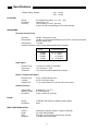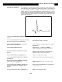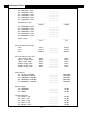
1
MODEL DS345 Synthesized Function Generator 1290-D Reamwood Avenue Sunnyvale, California 94089 Phone: (408) 744-9040 • Fax: (408) 744-9049 email: [email protected] • www.thinkSRS.com Copyright © 1993-99, 2009, 2012, 2015, 2016 by SRS, Inc. All Rights Reserved. Revision 2.3 (12/2016) DS345 Synthesized Function Generator Table of Contents GPIB and RS232 Setup Self-Test and Autocal Condensed Information SRS Symbols Safety and Use Specifications Abridged Command List iii iv v ix Arbitrary Waveform Editing Edit Menu Point Format Editing Point Format Example Vector Format Editing Vector Format Example Getting Started Introduction CW Function Generation Frequency Sweep Tone Bursts 1-1 1-1 1-2 1-3 2-1 DS345 Features Front Panel Features Rear Panel Features 2-5 2-5 2-7 Function Setting Setting the Function Frequency Amplitude DC Offset Phase 2-9 2-10 2-10 2-11 2-12 2-12 Sweeps and Modulation Modulation Parameters Modulation On/Off Modulation Type Modulation Rate Amplitude Modulation External AM Internal AM Frequency Modulation Phase Modulation Burst Modulation Burst Count Starting Point Frequency Sweeps Sweep Type Sweep Frequencies Sweep Markers Sweep Outputs Trigger Generator Arbitrary Modulation Patterns Pulse Generation 2-13 2-13 2-13 2-13 2-14 2-15 2-15 2-15 2-16 2-17 2-18 2-18 2-18 2-19 2-19 2-19 2-20 2-21 2-22 2-23 2-24 Instrument Setup Default Settings Store and Recall 2-25 2-25 2-25 2-29 2-29 2-30 2-31 2-32 2-33 Programming Programming the DS345 Communications GPIB Communication RS-232 Communication Data Window Operation Introduction to DDS 2-26 2-27 Command Syntax Detailed Command List Function Output Commands Modulation Control Arb Waveform and Modulation Setup Control Commands Status Reporting Commands Test and Calibration Commands Status Byte Definitions Programming Examples Arbitrary AM Modulation Arbitrary FM Modulation Arbitrary PM Modulation Point Mode Arb Waveform Vector Mode Arb Waveform 3-1 3-1 3-1 3-1 3-1 3-1 3-3 3-3 3-4 3-6 3-9 3-9 3-10 3-12 3-15 3-16 3-17 3-18 3-19 3-20 Test and Calibration i Troubleshooting Operation Error Messages Self-Test Error Messages Autocal Error Messages 4-1 4-1 4-3 4-4 Performance Tests Necessary Equipment 5-1 5-1 Functional Tests Front Panel Test Self Tests Sine Wave Square Wave Amplitude Flatness Output Level 5-2 5-2 5-2 5-2 5-2 5-3 5-3 DS345 Synthesized Function Generator For More Info Performance Tests Frequency Accuracy Amplitude Accuracy DC Offset Accuracy Subharmonics Spurious Signals Harmonic Distortion Phase Noise Square Wave Rise Time Square Wave Symmetry AM Envelope Distortion 5-5 5-5 5-5 5-7 5-7 5-8 5-8 5-9 5-10 5-10 5-10 Test Scorecard 5-11 Calibration Introduction Calibration Enable Calbytes 7-7 DS345 Circuitry 6-1 6-1 6-1 6-1 Circuit Description Bottom PC Board Power Supplies Microprocessor System Display and Keyboard Ribbon Cable, Trigger and Sync GPIB and RS232 Interfaces Output Amplifier Output Attenuator 8-1 8-1 8-1 8-1 8-1 8-2 8-2 8-3 8-3 Top PC Board Ribbon Cable, ADC, DACs Clocks DDS ASIC and Memory Amplitude and Sweep DACs DDS Waveform DAC DDS Output Filters and Doubler Sync and Gain Adjust 8-4 8-4 8-4 8-5 8-5 8-6 8-6 8-6 Necessary Equipment 6-3 Adjustments Clock Adjustment DAC Reference Voltage Output Amplifier Bandwidth Bessel Filter Adjustment Harmonic Distortion 6-3 6-3 6-4 6-4 6-4 6-5 Component Parts List Bottom PC Board and Front Panel Top PC Board Optional PC Board Miscellaneous Parts Calibration 5.00 V Reference Clock Calibration Attenuator Calibration Carrier Null Calibration Sinewave Amplitude Square Wave Amplitude Square Wave Symmetry 6-6 6-6 6-6 6-6 6-7 6-8 6-8 6-9 Schematic Circuit Diagrams Sheet No. Bottom PC Board Power Supplies 1/7 Microprocessor System 2/7 Display and Keyboard 3/7 Ribbon Cable, Trigger and Sync 4/7 GPIB and RS232 Interfaces 5/7 Output Amplifier 6/7 Output Attenuator 7/7 Arbitrary Waveform Software Introduction Installing AWC Getting Started with AWC Hardware Requirements 7-1 7-1 7-1 7-3 Menus File Menu Edit Menu Waveform Menu Send Data Menu Set DS345 Menu Trigger Menu Zoom Menu Help Menu 7-3 7-3 7-3 7-4 7-5 7-5 7-6 7-6 7-7 Data File Format 7-7 Top PC Board Ribbon Cable, ADC, DACs Clocks DDS ASIC and Memory Amplitude and Sweep DACs DDS Waveform DAC DDS Output Filters and Doubler Sync and Gain Adjust 1/7 2/7 3/7 4/7 5/7 6/7 7/7 Front Panel Keypad LED Display 1/2 2/2 Bottom PCB Component Placement Top PCB Component Placement ii 9-1 9-1 9-10 9-21 9-22 DS345 Synthesized Function Generator iii DS345 Synthesized Function Generator Safety and Preparation for Use WARNING: Dangerous voltages, capable of causing death, are present in this instrument. Use extreme caution whenever the instrument covers are removed. This instrument may be damaged if operated with the LINE VOLTAGE SELECTOR set for the wrong ac line voltage or if the wrong fuse is installed. LINE VOLTAGE SELECTION LINE FUSE The DS345 operates from a 100V, 120V, 220V, or 240V nominal ac power source having a line frequency of 50 or 60 Hz. Before connecting the power cord to a power source, verify that the LINE VOLTAGE SELECTOR card, located in the rear panel fuse holder, is set so that the correct ac input voltage value is visible. Verify that the correct line fuse is installed before connecting the line cord. For 100V/120V, use a 1 Amp fuse and for 220V/240V, use a 1/2 Amp fuse. LINE CORD The DS345 has a detachable, three-wire power cord for connection to the power source and to a protective ground. The exposed metal parts of the instrument are connected to the outlet ground to protect against electrical shock. Always use an outlet which has a properly connected protective ground. Conversion to other ac input voltages requires a change in the fuse holder voltage card position and fuse value. Disconnect the power cord, open the fuse holder cover door and rotate the fuse-pull lever to remove the fuse. Remove the small printed circuit board and select the operating voltage by orienting the board so that the desired voltage is visible when it is pushed firmly back into its slot. Rotate the fuse-pull lever back into its normal position and insert the correct fuse into the fuse holder. iv Specifications SPECIFICATIONS FREQUENCY RANGE Waveform Sine Square Ramp Triangle Noise Arbitrary Maximum Freq 30.2 MHz 30.2 MHz 100 KHz 100 KHz 10 MHz 10 MHz Resolution 1 µHz 1 µHz 1 µHz 1 µHz (Gaussian Weighting) 40 MHz sample rate OUTPUT Source Impedance 50 Ω Output may float up to ±40V (AC + DC) relative to earth ground. AMPLITUDE Range into 50Ω load (limited such that |Vac peak| + |Vdc| ≤ 5 V) Vrms Vpp dBm (50Ω) Function Max. Min. Max. Min. Max. Min. Sine Square Triangle Ramp Noise Arbitrary 10V 10V 10V 10V 10V 10V 10 mV 10 mV 10 mV 10 mV 10 mV 10 mV 3.54V 5V 2.89V 2.89V 2.09V n.a. 3.54 mV 5 mV 2.89 mV 2.89 mV 2.09 mV n.a. +23.98 +26.99 +22.22 +22.22 +19.41 n.a. -36.02 -33.0 -37.78 -37.78 -40.59 n.a. Resolution 3 digits (DC offset = 0V) Accuracy (with 0V DC Offset) Sine: 10Vpp 1µHz 100 kHz 20 MHz ±0.2 dB ±0.2dB ±0.5dB ±0.4 dB ±0.4dB ±0.5dB 30.2 MHz 5Vpp 0.01Vpp Square: 10Vpp 1µHz 100 kHz 20 MHz ±3 % ±6% ±15% ±5% ±8% ±18% 5Vpp 0.01Vpp v 30.2 MHz Specifications Triangle, Ramp, Arbitrary: DC OFFSET Range: Resolution: Accuracy: ±3% > 5Vpp ±5% < 5Vpp ±5V (limited such that |Vac peak| + |Vdc| ≤ 5 V) 3 digits (VAC = 0) 1.5% of setting + 0.2 mV (DC only) ±0.8 mV to ±80 mV depending on AC and DC settings WAVEFORMS Sinewave Spectral Purity Spurious: Phase Noise: -45 dBc (non-harmonic, typ.) -55 dBc in a 30 KHz band centered on the carrier, exclusive of discrete spurious signals (typ.) Subharmonic: < -50 dBc Harmonic Distortion: Harmonically related signals will be less than: Level Frequency Range < -55 dBc < -45 dBc < -35 dBc < -25 dBc DC .1 1 10 to 100 KHz to 1 MHz to 10 MHz to 30 MHz Square Wave Rise/Fall Time: Asymmetry: Overshoot: < 15 nS (10 to 90%), at full output < 1% of period + 4nS < 5% of peak to peak amplitude at full output Ramps, Triangle and Arbitrary Rise/Fall Time Linearity Settling Time 35 nS (10 MHz Bessel Filter) ±0.5% of full scale output < 1 µs to settle within 0.1% of final value at full output Arbitrary Function Sample Rate: Memory Length: Resolution: 40 MHz/N, N = 1 to 2 -1. 8 to 16,300 points 12 bits (0.025% of full scale) Range: Resolution: ±7199.999° with respect to arbitrary starting phase 0.001° 34 PHASE AMPLITUDE MODULATION Source: Depth: Rate: Distortion: Internal (sine, square, triangle, or ramp) or External 0 to 100% AM or DSBSC 0.001 Hz to 10 kHz internal, 20 kHz max external < -35dB at 1kHz, 80% depth vi Specifications DSB Carrier: Ext Input: < -35db typical at 1 kHz modulation rate (DSBSC) ±5V for 100% modulation, 100 kW impedance. FREQUENCY MODULATION Source: Rate: Span: Internal (sine, square, triangle, ramp) 0.001 Hz to 10 kHz 1 µHz to 30.2 MHz (100 kHz for triangle or ramp) PHASE MODULATION Source: Rate: Span: Internal (sine, square, triangle, ramp) 0.001 Hz to 10 kHz ±7199.999° FREQUENCY SWEEP Type: Waveform: Time: Span: Markers: Sweep Output: Linear or Log, phase continuous up, down, up-down, single sweep 0.001s to 1000s 1 µHz to 30.2 MHz (100 kHz for triangle,ramp) Two markers may be set at any sweep point (TTL output) 0 - 10 V linear ramp signal, syncronized to sweep BURST MODULATION Waveform: Frequency: Count: any waveform except NOISE may be BURST Sine, square to 1 MHz; triangle, ramp to 100 kHz; arbitrary to 40 MHz sample rate 1 to 30,000 cycles/burst (1µs to 500s burst time limits) TRIGGER GENERATOR Source: Rate: External: Output: Single, Internal, External, Line 0.001 Hz to 10 kHz internal (2 digit resolution) Positive or Negative edge, TTL input TTL output Accuracy Aging Input Output ±5 ppm (20 to 30° C) 5 ppm/year 10 MHz/N ± 2 ppm. N = 1 to 8. 1V pk-pk minimum input level. 10 MHz, >1 Vpp sine into 50 Ω TIMEBASE Optional Timebase Type: Stability: Aging: Short Term: Ovenized AT-cut oscillator < 0.01ppm, 20 - 60°C < 0.001ppm/day -11 < 5 x 10 1s Allan Variance vii Specifications GENERAL Interfaces RS232-C (300 to 19200 Baud, DCE) and IEEE-488.2 with free DOS Based Arbitrary Waveform Software All instrument functions are controllable over the interfaces. Weight Dimensions Power 10 lbs 8.5" x 3.5" x 13" (WHL) 50 VA, 100/120/220/240 Vac 50/60 Hz viii Abridged Command List Syntax Variables i,j are integers. Variable x is a real number in integer, real, or exponential notation. Commands which may be queried have a ? in parentheses (?) after the mnemonic. The ( ) are not sent. Commands that may only be queried have a '?' after the mnemonic. Commands which may not be queried have no '?'. Optional parameters are enclosed by {}. Function Output Control Commands AECL AMPL(?) x ATTL FREQ(?) x FSMP(?) x FUNC(?) i INVT(?)i OFFS(?)x PCLR PHSE(?) x Sets the output amplitude/offset to ECL levels (1Vpp, -1.3V offset). Sets the output amplitude to x. x is a value plus units indicator. The units can be VP (Vpp), VR (Vrms), or DB (dBm). Example: AMPL 1.00VR sets 1.00 Vrms. Sets the output amplitude/offset to TTL levels (5 Vpp, 2.5 V offset). Sets the output frequency to x Hz. Sets the arbitrary waveform sampling frequency to x Hz. Sets the output function. 0 = sine, 1 = square, 2 = triangle, 3 = ramp, 4 = noise, 5= arbitrary. Set output inversion on (i=1) or off (i=0). Sets the output offset to x volts. Sets the current waveform phase to zero. Sets the waveform output phase to x degrees. Modulation control commands *TRG BCNT(?) i DPTH(?) i FDEV(?) x MDWF(?) i MENA(?) i MKSP MRKF(?) i ,x MTYP(?) i PDEV(?) x RATE(?) x SPAN(?) x SPCF(?) x SPFR(?) x SPMK STFR(?) x TRAT(?) x TSRC(?) i Triggers bursts/single sweeps if in single trigger mode. Sets the burst count to i. Sets the AM modulation depth to i %. If i is negative sets DSBSC with i % modulation. Sets the FM span to x Hz. Sets the modulation waveform. 0 = single sweep, 1 = ramp, 2 = triangle, 3 = sine, 4 = square, 5 = arbitrary, 6 = none. Turns modulation on (i=1) or off (i=0). Sets the sweep markers to the extremes to the sweep span. Sets marker frequency i to x Hz. 0 = mrk start freq, 1 = stop freq, 2 = center freq, 3 = span. Sets the modulation type. 0 = lin sweep, 1 = log sweep, 2 = AM, 3 = FM, 4 = PM, 5 = Burst. Sets the phase modulation span to x degrees. Sets the modulation rate to x Hz. Sets the sweep span to x Hz. Sets the sweep center frequency to x Hz. Sets the sweep stop frequency to x Hz. Sets the sweep span to the sweep marker positions. Sets the sweep start frequency to x Hz. Sets the internal trigger rate to x Hz. Sets the trigger source. 0 = single, 1 = internal, 2 = + Ext, 3 = - Ext, 4 = line. Arbitrary Waveform and Modulation commands AMRT(?) i AMOD? i Sets the arbitrary modulation rate divider to i. Allows downloading a i point arbitrary modulation waveform if the modulation type is AM, FM, or PM. After execution of this query the DS345 will return the ASCII value 1. The binary waveform data may now be downloaded. ix Abridged Command List LDWF? i,j Allows downloading a j point arbitrary waveform of format i. i = 0 = point format, i= 1 = vector format. After execution of this query the DS345 will return the ascii value 1. The binary waveform data may now be downloaded. Setup Control Commands *IDN? *RCL i *RST *SAV i Returns the device identification . Recalls stored setting i. Clears instrument to default settings. Stores the current settings in storage location i. Status Reporting Commands *CLS *ESE(?) j *ESR? {j} *PSC(?) j *SRE(?) j *STB? {j} STAT? {j} DENA(?) j Clears all status registers. Sets/reads the standard status byte enable register. Reads the standard status register, or just bit j of register. Sets the power on status clear bit. This allows SRQ's on power up if desired. Sets/reads the serial poll enable register. Reads the serial poll register, or just bit n of register. Reads the DDS status register, or just bit n of register. Sets/reads the DDS status enable register. Hardware Test and Calibration Control *CAL? *TST? Starts autocal and returns status when done. Starts self-test and returns status when done. Standard Event Status Byte Status Byte Definitions bit 0 1 2 3 4 Serial Poll Status Byte bit name 0 Sweep Done 1 2 3 4 5 6 7 usage set when no sweeps in progress Mod Enable set when modulation is enabled User SRQ set when the user issues a front panel SRQ DDS set when an unmasked bit in DDS status byte is set MAV set when GPIB output queue is non-empty ESB set when an unmasked bit in std event status byte is set RQS SRQ bit No Command set when there are no unexecuted commands in input queue 5 6 7 name usage unused unused Query Error set on output queue overflow unused Execution Err set on error in command execution Command Err set on command syntax error URQ set on any front panel key press PON set on power on DDS Status Byte x bit 0 1 2 name Trig'd Trig Error Ext Clock 3 Clk Error 4 Warmup 5 6 7 Test Error Cal Error mem err usage set on burst/sweep trigger set on trigger error set when locked to an external clock set when an external clock error occurs set when the DS345 is warmed up set when self test fails set when autocal fails set on power up memory error Getting Started Introduction This section is designed to familiarize you with the operation of the DS345 Synthesized Function Generator. The DS345 is a powerful, flexible generator capable of producing both continuous and modulated waveforms of exceptional purity and resolution. The DS345 is also relatively simple to use, the following examples take the user step by step through some typical uses. Data Entry Setting the DS345's operating parameters is done by first pressing the key with the desired parameter's name on it (FREQ, for example, to set the frequency). Some parameters are labelled above the keys in light gray. To display these values first press the SHIFT key and then the labelled key. [SHIFT][SWP CF] for example, displays the sweep center frequency. Values are changed through the numeric keypad or the MODIFY keys. To enter a value simply type the new value using the keypad and complete the entry by hitting one of the UNITS keys. If the entry does not have units, any of the UNITS keys may be pressed. If an error is made, pressing the CLR key returns the previous value. The current parameter value may also be increased or decreased with the MODIFY keys. Pressing the UP ARROW key will increase the value by the current step size, while pressing the DOWN ARROW key will decrease the value by the current step size. If the entered value is outside of the allowable limits for the parameter the DS345 will beep and display an error message. Step Size Each parameter has an associated step size which may be an exact power of 10 (1 Hz, 10 Hz or 100 Hz for example), or may be an arbitrary value. If the step size is an exact power of 10, that digit of the display will flash. Pressing [STEP SIZE] displays the step size for the current parameter (the STEP LED will be lit). Pressing [STEP SIZE] again returns the display to the previously displayed parameter. The step size may be changed by typing a new value while the STEP LED is lit. Pressing the MODIFY UP ARROW key while the step size is displayed increases the step size to the next larger decade, while pressing the MODIFY DOWN ARROW key will decrease the step size to the next smaller decade. CW Function Generation Our first example demonstrates generating CW waveforms and the DS345's data entry functions. Connect the front panel FUNCTION output to an oscilloscope, terminating the output into 50 ohms. Turn the DS345 on and wait until the message "TEST PASS" is displayed. 1) Press [SHIFT][DEFAULTS]. This recalls the DS345's default settings. 2) Press [AMPL]. Then press [5][Vpp]. Displays the amplitude and sets it to 5 Vpp. The scope should show a 5 Vpp 1 kHz sine wave. 3) Press [FUNCTION DOWN ARROW] twice. The function should change to a square wave and then a triangle wave. 4) Press [FREQ] and then [1][0][kHz]. Displays the frequency and sets it to 10 kHz. The scope should now display a 10 kHz triangle wave. 1-1 1 Getting Started 5) Press [MODIFY UP ARROW]. The frequency will increment to 10.1 kHz. flashing digit indicates a step size of 100 Hz. 6) Press [STEP SIZE]. Observe that the step size is indeed 100 Hz. The STEP LED should be on. 7) Press [1][2][3][Hz]. Then press [STEP SIZE]. We've changed the step size to 123 Hz and displayed the output frequency again. 8) Press [MODIFY DOWN ARROW]. The frequency is decreased by 123 Hz to 9977 Hz. 9) Press [STEP SIZE] then [MODIFY UP ARROW] The step size is displayed and is increased from 123 Hz to the next larger decade–1 kHz. 10) Press [STEP SIZE]. The frequency is displayed again. The flashing digit indicates that the step size is 1 kHz. 11) Press [MODIFY UP ARROW]. The frequency is incremented to 10.977 kHz. Frequency Sweep The The next example sets up a linear frequency sweep with markers. The DS345 can sweep the output frequency of any function over any range of allowable output frequencies. There are no restrictions on minimum or maximum sweep span. The sweep time may range from 1 ms to 1000 s. The DS345 also has two independent rear-panel markers that may be used indicate specific frequencies in the sweep. The MARKER output goes high at the start marker position and low at the stop marker position. An oscilloscope that can display three channels is required. Attach the FUNCTION output BNC to the oscilloscope, terminating the output into 50 ohms. Set the scope to 2V/div. Attach the SWEEP rear-panel BNC to the scope and set it to 2V/div. The scope should be set to trigger on the falling edge of this signal. Attach the MARKER rear-panel BNC to the scope's third channel. This signal will have TTL levels. 1) Press [SHIFT][DEFAULTS]. This recalls the DS345's default settings. 2) Press [AMPL] then [5][Vpp]. Set the amplitude to 5Vpp. 3) Press [SWEEP MODE UP ARROW] twice. Set the modulation type to linear sweep. 4) Press [RATE] then [1][0][0][Hz]. Set the sweep rate to 100 Hz. The sweep will take 10 ms (1/100Hz). Set the scope time base to 1ms/div. 5) Press [START FREQ] then [1][0][0][kHz]. Set the sweep start frequency to 100 kHz. 1-2 Getting Started 6) Press [SHIFT][STOP F] then [1][MHz]. Set the stop frequency to 1 MHz. 7) Press [SWEEP ON/OFF]. This starts the sweep. The MOD/SWP LED will light, indicating that the DS345 is sweeping. The scope should show the SWEEP output as a 0V to 10 V sawtooth wave. The sweep starts at 100kHz when the sawtooth is at 0 V and moves to 1MHz when the sawtooth is at 10 V. The FUNCTION output is the swept sine wave. The markers are not yet active. 8) Press [SHIFT][MRK STOP] then [9][0][0][kHz]. Display the stop marker position and set the stop marker to 900 kHz. The marker should now be high from the start of the sweep to 900kHz (9V on the sweep sawtooth), then the marker should go low. 9) Press [SHIFT][MRK START] then [2][0][0][kHz]. Set the start marker to 200 kHz. The marker is now low from the beginning of the sweep until the 200 kHz start marker (2V on the sawtooth). The marker stays high until the 900 kHz stop marker. The markers allows designating any two frequencies in the sweep. 10) Press [SHIFT][SPAN=MRK]. This sets the sweep span to the marker positions. The sweep now goes from 200 kHz to 900 kHz. This function allows zooming in on any feature in the sweep without entering the frequencies. Tone Bursts This example demonstrates the DS345's tone burst capability. The DS345 can produce a burst of 1 to 30,000 cycles of any of its output functions. The bursts may be triggered by the internal rate generator, the line frequency, a front panel button, or an external rising or falling edge. The TRIGGER output goes high when the burst is triggered and low when the burst is over. Connect the DS345's FUNCTION output to an oscilloscope, terminating the output into 50 ohms. Set the sensitivity to 2V/div. Connect the rear-panel TRIGGER output to the scope and set 2V/div. Trigger the scope on the rising edge of the TRIGGER output. Set the scope timebase to 0.5ms/div. 1) Press [SHIFT][DEFAULTS]. This recalls the DS345's default settings. 2) Press [AMPL] then [5][Vpp]. Set the amplitude to 5Vpp. 3) Press [FREQ] then [1][0][kHz]. Set the output frequency to 10 kHz. This will be the frequency of the tone. 1-3 Getting Started 4) Press [SWEEP MODE DOWN ARROW] three times. Set the modulation type to BURST. 5) Press [SHIFT][BRST CNT]. Then [1][0][Hz]. Set the number of pulses in the burst to 10. Any of the units keys may be used to terminate the entry. 6) Press [SHIFT][TRIG SOURCE] Then press [MODIFY UP ARROW]. Display the burst trigger source. Then change the source from single trigger to the internal trigger rate generator. 7) Press [SHIFT][TRIG RATE] then [4][0][0][Hz]. Set the internal trigger rate generator to 400 Hz. 8) Press [SWEEP ON/OFF]. Enable the burst. The MOD/SWP LED will light. The scope should show two bursts of 10 cycles of a sine wave. 9) Press [SHIFT][BRST CNT]. Display the burst count again. 10) Press [MODIFY DOWN ARROW] twice. There should now be 8 pulses in each burst. 1-4 Introduction to Direct Digital Synthesis Introduction Direct Digital Synthesis (DDS) is a method of generating very pure waveforms with extraordinary frequency resolution, low frequency switching time, crystal clock-like phase noise, and flexible modulation. As an introduction to DDS let's review how traditional function generators work. Traditional Generators Frequency synthesized function generators typically use a phase-locked loop (PLL) to lock an oscillator to a stable reference. Wave-shaping circuits are used to produce the desired function. It is difficult to make a very high resolution PLL so the frequency resolution is usually limited to about 1:106 (some sophisticated fractional-N PLLs do have much higher resolution). Due to the action of the PLL loop filter, these synthesizers typically have poor phase jitter and frequency switching response. In addition, a separate wave-shaping circuit is needed for each type of waveform desired, and these often produce large amounts of waveform distortion. Arbitrary Waveforms Arbitrary function generators bypass the need for wave-shaping circuitry. Usually, a PLL is used to create a variable frequency clock that increments an address counter. The counter addresses memory locations in waveform RAM, and the RAM output is converted by a high speed digital-to-analog converter (DAC) to produce an analog waveform. The waveform RAM can be filled with any pattern to produce "arbitrary" functions as well as the usual sine, triangle, etc. The sampling theorem states that, as long as the sampling rate is greater than twice the frequency of the waveform being produced, with an appropriate filter the desired waveform can be perfectly reproduced. Since the frequency of the waveform is adjusted by changing the clock rate, the output filter frequency must also be variable. Arbitrary generators with a PLL suffer the same phase jitter, transient response, and resolution problems as synthesizers. DDS DDS also works by generating addresses to a waveform RAM to produce data for a DAC. However, unlike earlier techniques, the clock is a fixed frequency reference. Instead of using a counter to generate addresses, an adder is used. On each clock cycle, the contents of a Phase Increment Register are added to the contents of the Phase Accumulator. The Phase Accumulator output is the address to the waveform RAM (see diagram below). By changing the Phase Increment the number of clock cycles needed to step Direct Digital Synthesis DDS ASIC External Control Figure 1: Block diagram of SRS DDS ASIC Modulation CPU Modulation RAM Fixed Frequency Reference Phase Increment Register 48 Bits + 2-1 Phase Accumulator 48 bits Waveform RAM 16k points DAC Fixed Frequency Filter Introduction through the entire waveform RAM changes, thus changing the output frequency. Frequency changes now can be accomplished phase continuously in only one clock cycle. And the fixed clock eliminates phase jitter and requires only a simple fixed frequency anti-aliasing filter at the output. The DS345 uses a custom Application Specific Integrated Circuit (ASIC) to implement the address generation in a single component. The frequency resolution is equal to the resolution with which the Phase Increment can be set. In the DS345, the phase registers are 48 bits long, resulting in an impressive 1:1014 frequency resolution. The ASIC also contains a modulation control CPU that operates on the Phase Accumulator, Phase Increment, and external circuitry to allow digital synthesis and control of waveform modulation. The Modulation CPU uses data stored in the Modulation RAM to produce amplitude, frequency, phase, and burst modulation, as well as frequency sweeps. All modulation parameters, such as rate, frequency deviation, and modulation index, are digitally programmed. DDS gives the DS345 greater flexibility and power than conventional synthesizers or arbitrary waveform generators without the drawbacks inherent in PLL designs. DS345 Description Modulation RAM 40MHz Clock DDS345 ASIC Waveform RAM Cauer Filter 12 bit DAC x2 10 MHz Bessel Filter Sync Output Square Wave Comparator Function Output AM Input Amplitude DAC Amplitude Control Output Amp Attenuators Figure 2: DS345 Block Diagram A block diagram of the DS345 is shown in Figure 2. The heart of the DS345 is a 40 MHz crystal clock. This clock is internally provided, but may be phase locked to an external reference. The 40 MHz clock controls the DDS345 ASIC, waveform RAM, and high-speed 12bit DAC. Sampling theory limits the frequency of the waveform output from the DAC to about 40% of 40 MHz, or 15 MHz. The 48 bit length of the DDS345's PIR's sets the frequency resolution to about 146 nHz. These parameters and the DAC's 12 bit resolution define the performance limits of the DS345. 2-2 Introduction The reconstruction filter is key to accurately reproducing a waveform in a sampled data system. The DS345 contains two separate filters. For sine wave generation the output of the DAC goes through a 9th order Cauer filter, while ramps, triangles, and arbitrary waveforms pass instead through a 10 MHz 7th order Bessel filter. The Cauer filter has a cutoff frequency of 16.5 MHz and a stopband attenuation of 85dB, and also includes a peaking circuit to correct for the sine(x)/x amplitude response characteristic of a sampled system. This filter eliminates any alias frequencies from the waveform output and allows generation of extremely pure sine waves. The output of the Cauer filter is then frequency doubled by an analog multiplier. This multiplies the DAC's 0 - 15 MHz output frequency range to the final 0 - 30 MHz range. However, the Cauer filter has very poor time response and is only useful for CW waveforms. Therefore, the Bessel filter was chosen for its ideal time response, eliminating rings and overshoots from stepped waveform outputs. This filter limits the frequency of arbitrary waveforms to 10 MHz and rise times to 35 ns. The output of the filters pass to an analog multiplier that controls the amplitude of the waveform. This multiplier controls the waveform amplitude with an AM signal that may come from either the ASIC or the external AM input. This allows both internally and externally controlled amplitude modulation. The amplitude control is followed with a wide bandwidth power amplifier that outputs 10 V peak-to-peak into a 50 ohm load with a rise time of less than 15 ns. The output of the power amplifier passes through a series of three step attenuators (6, 12, and 24 dB) that set the DS345's final output amplitude. The post amplifier attenuators allow internal signal levels to remain as large as possible, minimizing output noise and signal degradation. Square waves and waveform sync signals are generated by discriminating the function waveform with a high-speed comparator. The output of the comparator passes to the SYNC OUTPUT and, in the case of square waves, to the amplitude control multiplier input. Generating square waves by discriminating the sine wave signal produces a square wave output with rise and fall times much faster than allowed by either of the signal filters. 2-3 Introduction 2-4 Front Panel Features 11 SRS 10 STANFORD RESEARCH SYSTEMS MODEL DS345 30MHz SYNTHESIZED FUNCTION GENERATOR STATUS REM SRQ ACT ERR TIMEBASE EXT ERR FUNCTION FREQ OUTPUTS 9 12 AMPL FUNCTION TRIG'D SYNC STEP TTL FUNCTION NOISE ARB TTL AMPL ECL 8 50Ω SPAN SINGLE MRK AM (INT) FM Φm BURST dBm Vrms % Vpp STRT f STOP f MODULATION ENTRY MODIFY MOD/SWP SHIFT SWEEP ON/OFF SHIFT STO RCL CLR BRST CNT GPIB SRQ RS232 DATA +/- 7 ARB RATE TRIG SWP CF OFFST SPAN (DEPTH) REL=0 STOP f PHASE START FREQ 7 RATE SWEEP/MODULATE LIN SWP LOG SWP FREQ 40V max. OFFS PHASE TRIG Hz DEG 6 ARB EDIT MRK START MRK STOP . 4 DEFAULTS CALIBRATE 8 9 MRK CF MRK SPAN 5 6 DEG % LOCAL kHz Vrms TRIG SOURCE TRIG RATE MRK=SPAN SPAN=MRK 0 5 1 2 3 3 2 MHz dBm STEP SIZE ON/STBY Hz Vpp 1 4 1) Power Switch The power switch turns the DS345 on and off. In the STBY position power is maintained to the DS345's internal oscillator, minimizing warmup time. 2) MODIFY Keys The modify keys permit the operator to increase or decrease the displayed parameter value. The step size may be determined by pressing the STEP SIZE key (the STEP LED will light). Every displayed parameter has an associated step size, pressing the MODIFY UP arrow key adds the step size to the current value, while pressing the MODIFY DOWN arrow key subtracts the step size from the current value. If the step size is set to an exact power of 10 (1, 10, or 100, for example) the corresponding digit of the display will flash. To change the step size, display the step size and then either enter a new value with the ENTRY keys or the MODIFY keys. Pressing the MODIFY UP arrow while the step LED is lit will increase the step size to the next larger decade, while pressing the MODIFY DOWN arrow will decrease the step size to the next smaller decade. The MODIFY UP/DOWN arrows also select between different menu selections (ie., trigger source). Sometimes the parameter display will have more than one parameter displayed at a time, and the [SHIFT][LEFT] and [SHIFT][RIGHT] keys will select between these values. 3) ENTRY Keys The numeric keypad allows for direct entry of the DS345's parameters. To change a parameter value simply type the new value using the keypad. The value is entered by terminating the entry with one of the UNITS keys. A typing error may be corrected by using the CLR key. The +/- key may be selected at any time during number entry. 4) Units Keys The UNITS keys are used to terminate numeric entries. Simply press the key with the desired units to enter the typed value. Some parameters don't have 2-5 DS345 FEATURES any associated units and any of the units keys may be used to enter the value. When the amplitude is displayed, pressing a units key without entering a new value will displayed the amplitude in the new units. This allows the amplitude display to be switched between Vpp, Vrms, and dBm without entering a new value. 5) Shift Key The shift key is used to select the functions printed in gray above the keys. Press [SHIFT] and then [key] to select the desired function (for example [SHIFT][SWP CF] to display the sweep center frequency). When the SHIFT key is pressed the SHIFT LED will light. This indicates that the keyboard is in shift mode. Pressing [SHIFT] a second time will deactivate shift mode. 6) Modulation Keys These keys control the DS345's modulation capabilities. The MODULATION TYPE up/down arrow keys select the modulation type. The MODULATION WAVEFORM up/down arrow keys select the waveform of the modulating function. The [SWEEP ON/OFF] key turns the modulation on and off. When the modulation is turned on the MOD/SWP LED will light. If the modulation parameters are not permitted for the selected output function, an error message will be displayed and modulation will not be turned on. Some modulation parameters are not relevant to all modulation types (start frequency is not relevant to AM, for example), and the message "NOT APPLIC" will be displayed if they are selected. 7) Function Keys These keys choose the main function output. The FUNCTION up/down arrow keys select between the output functions. If the output frequency is set beyond of the range allowed for a waveform (> 100 kHz for triangle and ramp) a message will be displayed and the frequency will be set to the maximum allowed for that function. 8) Main Function BNC This output has an impedance of 50Ω. If it is terminated into an impedance other than 50Ω the output amplitude will be incorrect and may exhibit increased distortion. The shield of this output may be floated up to ±40V relative to earth ground. 9) Sync Output BNC This output is a TTL square wave synchronized to the main function output and has a 50Ω output impedance. The shield of this output may be floated up to ±40V relative to earth ground. 10) Status LEDs These six LEDs indicate the DS345's status. The LED functions are: name function REM The DS345 is in GPIB remote state. The STEP SIZE key returns local control. SRQ The DS345 has requested service on the GPIB interface. ACT Flashes on RS232/GPIB activity. ERR Flashes on an error in the execution of a remote command. EXT CLOCK The DS345 has detected a signal at its TIMEBASE input and is trying to phase lock to it. CLOCK ERR The DS345 is unable to lock to the signal at the TIMEBASE input. This is usually because the signal is too far (>2ppm) from the nominal values of 10, 5, 3.33, 2.5 or 1.25 MHz. 11) Parameter Display This 12 digit display shows the value of the currently displayed parameter. The LEDs below the display indicate which parameter is being viewed. Error messages may also appear on the display. When an error message is displayed you can return to the normal operation by pressing any key. 2-6 DS345 FEATURES These LEDs indicate the units of the displayed value. If no LED is lit the number displayed has no units. 12) Units LEDs Rear Panel Features 1 TRIGGER 2 TTL TRIGGER TTL 3 SWEEP 0-10V ! INPUTS AM(EXT) 0-5V OUTPUTS MODULATION 0-5V MARKER TTL TIMEBASE 10MHz 10MHz FUSE: 3/4A (100/120VAC) or 3/8A (220/240VAC) 1V BLANK/LIFT TTL WARNING: No user serviceable parts inside. Refer to operation manual for safety notice. For use by qualified laboratory personnel only. IEEE-488 STD PORT (GPIB) 4 1) Power Entry Module RS232 (DCE, 8d, 0p, 2s bits) 5 This contains the DS345's fuse and line voltage selector. Use a 1 amp fuse for 100/120 volt operation, and a 1/2 amp fuse for 220/240 volt operation. To set the line voltage selector for the correct line voltage first remove the fuse. Then, remove the line voltage selector card and rotate the card so that the correct line voltage is displayed when the card is reinserted. Replace the fuse. 2) External Inputs Trigger Input The trigger input is a TTL compatible input used to trigger modulation sweeps and bursts. This input has a 10 kΩ input impedance. The shield of this input is tied to that of the function output and may be floated up to ±40V relative to earth ground. AM Input The AM input controls the amplitude of the function output. This input has a 100 kΩ input impedance and a ±5V range, where +5V sets the output to 100% of the front panel setting, 0V sets the output to 0, and -5V sets the output to -100% of the setting. The 0 to 5V range is used for normal AM operation, while the ±5V range is used for DSBSC modulation. This input is always active and should only be be connected if AM is desired. The shield of this input is tied to the shield of the function output and may be floated up to ±40V relative to earth ground. 2-7 DS345 FEATURES Timebase Input This 1kΩ impedance input allows the DS345 to lock to an external timebase. The external source should be greater than 1V pk-to-pk and should be within ±2 ppm of 10 MHz or any subharmonic down to 1.25 MHz. The shield of this input is connected to earth ground. 3) Auxiliary Outputs 10 MHz Output This output produces a >1V pk-pk 10 MHz sinewave from the DS345's internal oscillator. It expects a 50Ω termination. The shield of this output is connected to earth ground. Modulation Out This output generates a 0 - 5V representation of the current modulation function. The shield of this output is tied to that of the function output and may be floated up to ±40V relative to earth ground. Trigger Output This TTL compatible output goes high when a triggered sweep or burst begins, and goes low when it ends. This may be used to synchronize an external device to the sweep/burst. The shield of this output is tied to that of the function output and may be floated up to ±40V relative to earth ground. Sweep Output This output generates a 0 - 10 V ramp that is synchronous with the DS345's frequency sweep. The shield of this output is tied to that of the function output and may be floated up to ±40V relative to earth ground. Marker Output This TTL compatible output goes high when the DS345's frequency sweep passes the start marker frequency, and goes low when the sweep passes the stop marker frequency. The shield of this output is tied to that of the function output and may be floated up to ±40V relative to earth ground. Blank/Lift Out This TTL compatible output is low during the upsweep of a frequency sweep, and is high during the sweep retrace. The shield of this output is tied to that of the function output and may be floated up to ±40V relative to earth ground. 4) GPIB Connector If the DS345 has the optional GPIB/RS232 interface this connector is used for IEEE-488.1 and .2 compatible communications. The shield of this connector is connected to earth ground. 5) RS232 Connector If the DS345 has the optional GPIB/RS232 interface this connector is used for RS232 communication. The DS345 is a DCE and accepts 8 bits, no parity, 2 stop bits and 300 and 19.2k Baud. The shield of this connector is connected to earth ground. 2-8 DS345 OPERATION Introduction The following sections describe the operation of the DS345. The first section describes the basics of setting the function, frequency, amplitude, and offset. The second section explains sweeps and modulation. The third section explains storing and recalling setups, running self-test and autocalibration, and setting the computer interfaces. The fourth and last section describes front panel editing of arbitrary waveforms. Power-On When the power is first applied to the DS345 the unit will display its serial number and ROM version for about three seconds. The DS345 will then initiate a series of self-tests of the circuitry and stored data. The test should take about three seconds and end with the message "TEST PASS". If the self test fails the DS345 will display an error message indicating the nature of the problem (see the TROUBLESHOOTING section for more details, page 41). The DS345 will attempt to operate normally after a self-test failure, (pressing any key will erase the error message). SETTING THE FUNCTION TRIG'D SYNC FREQ TTL NOISE ARB TTL AMPL ECL FUNCTION OFFST REL=O 40V max OUTPUTS 50 Ω PHASE The FUNCTION and SYNC BNCs are the DS345's main outputs. Both of these outputs are fully floating, and their shields may be floated relative to earth ground by up to ±40V. Both outputs also have a 50Ω output impedance. If the outputs are terminated into high impedance instead of 50Ω the signal levels will be twice those programmed (the FUNCTION output may also show an increase in waveform distortion). The programmed waveform comes from the FUNCTION output, while the SYNC output generates a TTL compatible (2.5 V into 50Ω) signal that is synchronous with the function output. The SYNC signal is suppressed if the function is set to NOISE or BURST modulation. If the function is set to ARB the SYNC signal is a 25ns negative going pulse at the start of each waveform. 2-9 Function Setting FUNCTION SELECTION The DS345's output function is selected using the FUNCTION UP/DOWN arrow keys. Simply press the keys until the desired function LED is lit. If the programmed frequency is outside of the range allowed for the selected function, an error message will be displayed and the frequency will be set to the maximum allowed for that function. If modulation is enabled and the modulation type or parameters are incompatible with the new function, an error message will be displayed and the modulation will be turned off (the parameters will not be altered). Ramps Ramp functions usually ramp up in voltage, however, downward ramps may be programmed with the output invert function (see AMPLITUDE section). Arbitrary Functions Arbitrary functions may be created on a computer and downloaded to the DS345 via the computer interfaces, or they may be created using the DS345's front panel editing functions. Arbitrary waveforms normally repeat continuously, single triggering and burst triggering of arbitrary waveforms is accomplished using the DS345's BURST modulation function. (See the ARBITRARY WAVEFORM EDITING section for more detail.) FREQUENCY To display the DS345's output frequency press [FREQ]. The frequency is always displayed in units of Hz. The DS345 has 1 µHz frequency resolution at all frequencies, for all functions. The maximum frequency depends on the Function Frequency Range Sine 1 µHz → 30.200000000000 MHz Square 1 µHz → 30.200000000000 MHz Triangle 1 µHz → 100,000.000000 Hz Ramp Noise Arbitrary 1 µHz → 100,000.000000 Hz 10 MHz White Noise (fixed) 0.002329Hz → 40.0 MHz sampling function selected as listed below: Frequency is usually displayed by the DS345 with 1 mHz resolution. However, if the frequency is below 1 MHz and the microhertz digits are not zero the DS345 will display the frequency with 1 µHz resolution. At frequencies greater than 1 MHz the digits below 1 mHz cannot be displayed, but the frequency still has 1 µHz resolution and may be set via the computer interfaces or by using the MODIFY keys with a step size less than 1 mHz. If the function is set to NOISE the character of the noise is fixed with a band limit of 10 MHz. The frequency is not adjustable and the FREQ display will read "noise" instead of a numerical value. If the function is set to ARB the frequency displayed is the sampling frequency of the arbitrary waveform. This number is independent of the usual frequency; it is the dwell time that the DS345 spends on each point in an arbitrary waveform. This sampling frequency must be an integer submultiple of the the 40 MHz clock frequency. That is, 40 MHz/N where N = 1,2,3... 234-1 (40 MHz, 20 MHz, 13.3333 MHz, 10 MHz, ...). The DS345 will spend 2-10 Function Setting 1/Fsample on each point. When a new sampling frequency value is entered the DS345 will round the value to the nearest integer submultiple of 40 MHz. Note that the frequency for the standard functions is never rounded. Setting the Frequency To set the frequency of any function simply type a new value on the keypad and complete the entry with the appropriate units (Hz, kHz, or MHz). The MODIFY keys may be used to increase or decrease the frequency by the current step size. Press [STEP SIZE] key to display and change the step size. AMPLITUDE Pressing [AMPL] displays the amplitude of the output function. The amplitude may be set and displayed in units of Vpp, Vrms, and dBm. The current units are indicated by the LEDs at the right of the display. The amplitude range is limited by the DC offset setting since |Vac peak | + |Vdc| ² 5 V. If the DC offset is zero the amplitude range for each of the functions is shown below: note: The rms and dBm values for NOISE are based on the total power in the output bandwidth (about 10 MHz) at a given peak to peak setting. Vpp Vrms dBm (50Ω) Function Max. Min. Max. Min. Max. Min. Sine Square Triangle Ramp Noise Arbitrary 10V 10V 10V 10V 10V 10V 10 mV 10 mV 10 mV 10 mV 10 mV 10 mV 3.54V 5V 2.89V 2.89V 2.09V n.a. 3.54 mV 5 mV 2.89 mV 2.89 mV 2.09 mV n.a. +23.98 +26.99 +22.22 +22.22 +19.41 n.a. -36.02 -33.0 -37.78 -37.78 -40.59 n.a. Arbitrary function amplitude may only be set in units of Vpp. The output signal will briefly go to zero as the output attenuators are switched. The units of the amplitude display may be switched between Vpp, Vrms, and dBm without changing the actual amplitude by pressing the corresponding units key. When the DS345 is switched from one function to another the peak-to-peak amplitude is held constant. If the DC offset is zero, the amplitude may be set with three digits of resolution. If the DC offset is not zero the larger of the amplitude and the offset determines the resolution of both parameters. The amplitude display is automatically adjusted such that all of the digits that may be changed are displayed. Output Inversion For ramp and arbitrary functions the DS345's output may be inverted. This is useful for turning positive ramps into negative ramps, or inverting arbitrary waveforms. Pressing [AMPL] two times displays the invert enable option. Use the UP/DOWN MODIFY keys to enable or disable the inversion. D.C. Only The output of the DS345 may be set to a DC level by entering an amplitude of 0V. When the amplitude is set to zero the A.C. waveform will be off and the DS345 may be used as a DC voltage source. If the amplitude is zero the display will read "no AC" when the units are set to dBm. TTL Settings Pressing [SHIFT][TTL] sets the output amplitude and offset to TTL values. 2-11 Function Setting TTL levels are 5 Vpp with a 2.5V offset (the output will swing between 0 and +5V). ECL Settings Pressing [SHIFT][ECL] sets the output amplitude and offset to ECL values. ECL levels are 1 Vpp with a -1.3V offset (the output will swing between -1.8V and -0.8V). DC OFFSET The DC offset may range between ±5V, but is restricted such that |Vac peak | + |Vdc| ² 5 V. When [OFFST] is pressed a new value may be entered using any amplitude unit key, the Vpp indicator LED will be lit . When the offset is changed the output signal will briefly go to zero as the output attenuators are switched. If the amplitude is zero, the offset may be set with three digits of resolution. If the amplitude is not zero the larger of the amplitude and offset determines the resolution of both parameters. The offset display is automatically adjusted such that all of the digits that may be changed are displayed. PHASE Press [PHASE] to display and modify the phase of the FUNCTION output. Phase is always measured with respect to the internal timebase, not the SYNC output. The phase may be changed with the keypad and the DEG unit key, or using the MODIFY keys. The range of the phase setting is ±7199.999° and may be set with 0.001° resolution. If the function is set to NOISE, ARB, or modulation is enabled in SWEEP, FM, or PM modes the phase cannot be changed and the message "no Phase" will be displayed. In BURST modulation mode the PHASE function will set the waveform phase at the start of the burst. This is quite useful for starting the burst at a particular point in the waveform. Zero Phase The current phase may be assigned the value zero by pressing [SHIFT] [REL=0]. Subsequent changes to phase will be relative to this value. 2-12 SWEEPS AND MODULATION Introduction This section of the manual describes the DS345's modulation capabilities. The DS345 has extremely powerful and flexible built-in modulation functions. It is capable of AM (both simple and double sideband suppressed carrier (DSBSC)), FM, PM, tone bursts, and frequency sweeps. The modulation waveform may be a sine, square, ramp, or triangle wave. Frequency can be swept up or down at a linear or logarithmic rate. A built-in trigger generator allows triggering of single sweeps and bursts. For additional flexibility the DS345 can also modulate the output waveform with an arbitrary pattern of amplitude, frequency, or phase values. SWEEP/MODULATE LIN SWP LOG SWP SINGLE SWEEP ON/OFF AM (INT) FM BRST CNT Im BURST MOD/SWP ARB RATE TRIG SWP CF SPAN (DEPTH) STOP f START FREQ MODULATION ON/OFF The SWEEP ON/OFF key enables the DS345's modulation functions. Pressing the key toggles the modulation status. When modulation is on the [MOD/SWP] LED will light. When modulation is enabled the modulation type and modulation parameters are checked for consistency with the selected output function. If the selected modulation is illegal (for example, FM frequency out of range for the function) the DS345 will display an error message and not enable the modulation. The erroneous value must be changed before the modulation is turned on. MODULATION TYPE The type of modulation is selected using the MODULATION TYPE [UP/ DOWN] arrow keys. Most of the output functions can be modulated by any type of modulation. However, NOISE can only be modulated by the external AM input, and ARB waveforms can only be modulated by AM and BURST modulations. If an invalid choice is selected the message "funct error" is displayed. MODULATION WAVEFORM The waveform of the modulating function is selected with MODULATION WAVEFORM UP/DOWN arrow keys. If no LEDs are lit the selected modulation type has no associated waveform (BURST, for example, has no modulation waveform). Not all modulation types may use all modulation waveforms. The allowable combinations are listed on the following page. Note that ARB modulation waveforms can only be downloaded via the computer interfaces. 2-13 Modulation and Sweeps If no waveform has been downloaded when this modulation is enabled the message "arb corrupt" will be displayed (see the ARBITRARY MODULATION section). WF Single Ramp Triangle Sine Square Arb None Yes Yes No No No No Yes Yes Yes Yes Yes No Yes Yes Yes Yes Yes No No No Yes Yes Yes No No No Yes Yes Yes No No No Yes Yes Yes No No No No No No Yes Type Linear Swp Log Swp AM FM PM Burst Table 1: Allowed modulation waveforms for each modulation type MODULATION RATE Pressing [RATE] displays and sets the modulation rate. Use the keypad and unit indicators of Hz, kHz, or MHz (or the MODIFY up/down keys) to set the modulation rate. The modulation rate is the frequency of the modulation waveform. For example, if the modulation type is AM, the waveform a sine wave, and the rate 1 kHz the modulating waveform will be a 1 kHz sine wave. For sweeps the modulation rate is the inverse of the sweep time (ie., a 10ms sweep would be entered as 100 Hz). Burst modulation has no associated modulation rate and the message "not applic" is displayed if [RATE] is pushed. The modulation rate has a range of 0.001 Hz to 10 kHz for AM, FM, and PM. The range for sweeps is 0.001 Hz to 1 kHz (1000s to 0.001s sweep time). The modulation rate may be set with two digits of resolution. If the modulation waveform is set to ARB (AM ARB, FM ARB, or PM ARB) the modulation rate has a different meaning. See the ARBITRARY MODULATION section for more details. 2-14 Modulation and Sweeps AMPLITUDE MODULATION Introduction The DS345 has the ability to amplitude modulate its function output with both the internal modulation generator and an external analog voltage. The internal modulation generator may modulate the output with a sine, square (pulse modulation), triangle, ramp, or arbitrary modulation pattern. The external modulation may be either simple AM or Double Sideband Suppressed Carrier (DSBSC) modulation. External AM Source The rear-panel AM INPUT is active at all times (even in concert with any other modulation type). The AM INPUT has an input voltage range of ±5V. A +5V input produces an output that is 100% of the programmed value, a 0V input turns the output will off (0%), and at -5V input produces an output that is -100% of the programmed output (a 180° phase change). Applying voltages from 0 to 5V will result in simple AM. If the voltages are balanced around zero (from -5V to +5V) DSBSC modulation will result (for good carrier suppression the modulating signal must have an average value of zero). The AM INPUT has a bandwidth of about 20 kHz. INTERNAL AM The internal modulation generator can modulate any of the DS345's output functions except NOISE. The modulating waveform may be a sine, square, triangle, ramp, or arbitrary pattern. The rear-panel MODULATION OUTPUT outputs a signal corresponding to the amplitude control voltage. 100% of the output amplitude will produce an output of +5V, zero output will produce 0V, and -100% output will produce -5V out. Modulation Depth Press [DEPTH] to display and set to the AM modulation depth. The value may be set using the keypad and % units key, or the MODIFY keys. This value has a range of ±100% with 1% resolution. Positive values (0 to100%) will set simple AM with a modulation percentage equal to the DEPTH. Zero percent depth corresponds to no modulation, while 100% depth corresponds to modulating the output from full off to full on. Negative values (-1% to -100%) will set DSBSC modulation with a modulation percentage equal to the depth. Modulation Rate Press [RATE] to display and to set the frequency of the modulating function. The frequency may be set with two digits of resolution from 0.001 Hz to 10 kHz. 2-15 Modulation and Sweeps FREQUENCY MODULATION Introduction The DS345 is capable of frequency modulating any of its output functions, except NOISE and ARB, using its internal modulation generator. The modulation waveform may be a sine, square (FSK), triangle, ramp, or an arbitrary pattern. The rear-panel MODULATION OUTPUT outputs a signal with 0V corresponding to the smallest frequency output and +5V corresponding to the largest frequency output. Frequency Span During FM the DS345 outputs a signal whose frequency range is centered about the programmed frequency. SPAN sets the amount that the frequency varies from the center frequency. The minimum frequency output will be the center frequency - SPAN/2, while the maximum frequency will be the center frequency + SPAN/2. The value SPAN/2 is commonly called the deviation (that is, SPAN = Deviation x 2). The SPAN is displayed and set by pressing [SPAN]. The SPAN may be set with 1 µHz resolution, and has a limited range such that the output frequency is always greater than zero and less than or equal to the maximum allowed for the function selected (30.2 MHz for sine and square, 100 kHz for triangle and ramp). Modulation Rate Pressing [RATE] displays and sets the frequency of the modulating function. The frequency may be set with two digits of resolution from 0.001 Hz to 10 kHz. 2-16 Modulation and Sweeps PHASE MODULATION Introduction The DS345 is capable of phase modulating any of its output functions, except NOISE and ARB, using its internal modulation generator. The modulation waveform may be a sine, square (PSK), triangle, ramp, or arbitrary pattern (see ARBITRARY MODULATION section for information about ARB patterns). The rear-panel MODULATION OUTPUT outputs a signal with 0V corresponding to the largest negative phase deviation and +5V corresponding to the largest positive phase deviation. Phase Span During PM the DS345 outputs a signal whose frequency is centered about the programmed frequency. SPAN sets the amount that the phase varies relative to zero phase. The minimum phase shift output will be -SPAN/2, while the maximum phase shift output will be +SPAN/2. The value SPAN/2 is commonly called the deviation (that is, SPAN = Deviation x 2). The SPAN is displayed and set by pressing [SPAN]. The value of the SPAN may be set with 0.001° resolution with a range of 0° to 7199.999°. Modulation Rate Press [RATE] to display and set the frequency of the modulating function. The frequency may be set with two digits of resolution in the 0.001 Hz to 10 kHz range. 2-17 Modulation and Sweeps BURST MODULATION Introduction The DS345 generates tone bursts of any of its periodic output functions. The frequency of the output function is limited to 1 MHz for sine and square waves, 100 kHz for triangles and ramps, and no limits for ARBs. When a trigger signal is received the DS345 initiates a burst starting at a specific point (phase) in the output waveform, outputs the exact number of programmed waveform cycles, and then stops. The rear-panel TRIGGER OUTPUT generates a TTL compatible signal that goes high when the burst is triggered and low when the burst is complete. This signal may be used to synchronize external equipment to the burst. The SYNC output is not active during tone bursts. Burst Count The number of complete cycles in a burst is set by pressing [SHIFT][BRST CNT]. The number may be set from 1 to 30000 cycles. The maximum time for a complete burst is 500s, the time for a burst is easily computed from the following formulas: Burst Time = Burst Count Frequency Burst Time = for sine, square, triangle, ramp Burst Count × # Waveform Points for Sampling Frequency ARB Waveform Starting Point The point in the waveform at which the burst starts (the phase) may be adjusted for sine, square, triangle, and ramp waves. For ARBs the burst always starts on the first waveform point. Changing the PHASE changes the point at which the burst starts. 0.000 degrees phase corresponds to the positive zero crossing of the function, and values up to 359.999 degrees increment through the waveform. PHASE values larger than 360 degrees are set to modulo 360 degrees. Triggering a Burst Burst modulation is a triggered function, and therefore a signal needs to initiate the burst. The trigger generator can initiate a burst from the front panel [TRIG] key, the internal rate generator, the external trigger input, or the power line frequency. Setting the trigger generator is detailed in the TRIGGER GENERATOR section (2-22). The TRIG'D LED flashes green each time a burst is triggered. If the DS345 is triggered before the previous burst is complete the TRIG'D LED flashes red, indicating a trigger error. At high trigger rates a combination of triggers (green) and trigger errors (red) can make the TRIG'D LED appear orange. Once a burst is triggered the DS345 will ignore all other triggers until the burst is complete. 2-18 Modulation and Sweeps FREQUENCY SWEEPS Introduction The DS345 can frequency sweep its function output for sine, square, triangle, and ramp waves. The sweeps may be up or down in frequency, and may be linear or log in nature. The frequency changes during the sweep are phase continuous and the sweep time may be set between 0.001 and 1000 seconds. The DS345 has an analog SWEEP output that may be used to drive an x-y recorder or oscilloscope, a TTL BLANK/LIFT output that can lift a chart recorder pen during the sweep retrace, and a TTL MARKER output that may be set to make transitions at two programmable frequencies during the sweep. Sweep Type Pressing the MODULATION TYPE UP/DOWN ARROW keys sets the sweep to either a linear or log sweep. The output frequency in a linear sweep changes linearly during the sweep time. The output frequency in a log sweep changes exponentially during the sweep time, spending an equal amount of time in each decade of frequency. For example, in a sweep from 1 kHz to 100 kHz, the sweep will spend half the time in the 1 kHz to 10 kHz range and half the time in the 10 kHz to 100 kHz range). It should be noted that these are digital sweeps, and that the sweep is actually composed of 1500 to 3000 discrete frequency points, depending on the sweep rate. Sweep Waveform The DS345's sweep waveform may be set to single, triangle, or ramp using the MODULATION WAVEFORM UP/DOWN arrow keys. With the SINGLE setting the DS345's output frequency will be the sweep start frequency until a trigger is received. The output will then sweep to the stop frequency, reset to the start frequency and wait for another trigger (see the TRIGGER GENERATOR section for setting the trigger source). If the waveform is set to a RAMP the DS345 will sweep from the start to the stop frequency, jump back to the start frequency, and repeat continuously. If the waveform is a TRIANGLE the DS345 will sweep from the start to the stop frequency, sweep back from the stop frequency to the start frequency, and repeat continuously. Sweep RATE/Time The duration of the sweep is set by [RATE], and the value is entered or modified with the keypad. The sweep rate may be set over the range of 0.001 Hz to1 kHz. The sweep rate is the inverse of the sweep time, a 0.001 Hz rate is equal to a 1000s sweep time, and a1 kHz rate is equal to a 1 ms sweep time. For a TRIANGLE sweep the sweep time is the total time to sweep up and down. SWEEP FREQUENCIES The DS345 may sweep over any portion of its frequency range:1 µHz to 30.2 MHz for sine and square waves, and 1 µHz to 100 kHz for triangle and ramp waves. There are no restrictions on minimum or maximum sweep span. The DS345's sweep range may be set by entering either the start and stop frequencies, or the center frequency and span. The relationships between the frequencies are: Center Frequency Span Start Frequency Stop Frequency 2-19 = (Stop Frequency + Start Frequency) / 2 = Stop Frequency - Start Frequency = Center Frequency - Span/2 = Center Frequency + Span/2 Modulation and Sweeps To enter the sweep start frequency press [START FREQ]. Set the stop frequency by pressing [SHIFT][STOP F]. The start and stop frequencies may have any values that are allowed for the displayed waveform. If the stop frequency is greater than the start frequency the DS345 will sweep up, while if the start frequency is larger the DS345 will sweep down. Center Frequency and Span To set the sweep center frequency press [SHIFT][SWP CF]. The center frequency may be set to any value allowed for the displayed waveform. Set the sweep span by pressing [SPAN]. The span value is restricted to sweep frequencies greater than zero and less than or equal to the maximum allowed frequency. If the span is positive the DS345 will sweep up, if it is negative the DS345 will sweep down. The MODIFY keys may be used to change the span: pressing [MODIFY UP] will double the span, while pressing [MODIFY DOWN] divides the span in half. The MODIFY keys affect the span in octaves–the size of the step is the value displayed by the step size. When the center frequency is changed the span is held constant, while changing the span holds the center frequency constant. If the center frequency or span is changed such that the sweep frequencies are out of the allowed range an error will be displayed on the front panel. SWEEP MARKERS The DS345 has two sweep markers that may be used to indicate any two frequencies in the sweep. The MARKER output is a TTL compatible signal that goes high when the sweep frequency crosses the start marker frequency and low when the sweep frequency crosses the stop marker frequency. In a triangle sweep the markers are only active on the up sweep. The marker positions may be set by entering the marker start and stop frequencies, or the center frequency and span. Marker Start and Stop The marker start and stop frequencies are independent of each other and are set by pressing [SHIFT][MRK START] and [SHIFT][MRK STOP] respectively. The frequencies can be set to any value from 1 µHz to 30.2 MHz. If the marker start frequency is lower than the marker stop frequency the MARKER output will initially be low, go high when the sweep crosses the start marker position, and go low again when the sweep crosses the stop marker position. If the marker start frequency is greater than the marker stop frequency the MARKER output will be initially high, go low when the sweep crosses the stop marker position, and go high again when the sweep crosses the start marker position. If either of the marker positions are outside of the sweep range the marker output will behave as if the sweep had crossed its position. These cases are shown in the diagram below: Mrk Stop Mrk Start Start and Stop Frequencies Case 3: Marker Start Freq < Sweep Start Freq 2-20 Sweep Stop Frequency Mrk Start Case 2: Marker Start Freq > Marker Stop Freq Mrk Stop Sweep Start Frequency Mrk Start Mrk Stop Case 1: Marker Start Freq < Marker Stop Freq Figure 1: Marker Output for different relationships between the marker start and stop frequencies. Modulation and Sweeps Marker Center and Span The markers may also be set by the center frequency and span (width) of the marked region. Pressing [SHIFT][MRK CF] and [SHIFT][MRK SPAN] respectively sets the center frequency and span. The center frequency may have any value from 1 µHz to 30.2 MHz range. The span may be any value such that the marker frequencies are greater than zero and less than or equal to 30.2 MHz. If the span is positive the marker start position will be below the stop position, while if the span is negative the marker start position will be greater than the stop position. If the MODIFY keys are used to change the span- pressing [MODIFY UP] will double the span, and pressing [MODIFY DOWN] will divide the span in half. When the center frequency is changed the span is held constant, while changing the span holds the center frequency constant. If the center frequency or span is changed such that the marker frequencies are out of the allowed range an error will be displayed. Marker to Span Pressing [SHIFT][MRK=SPAN] sets the positions of the markers to the extremes of the sweep span. The marker start frequency will be set to the sweep start frequency, and the marker stop frequency will be set to the sweep stop frequency. This function is useful for finding the markers when setting up a sweep. Span to Marker Press [SHIFT][SPAN=MRK] to set the sweep span to the marker positions. Now the sweep start frequency will be set to the marker start frequency, and the sweep stop frequency will be set to the marker stop frequency. This function can be used to "zoom in" on a marked section of the sweep. If this function sets the sweep frequencies to a value not allowed for the selected waveform, an error will be generated and the sweep disabled. SWEEP OUTPUT The rear-panel SWEEP output is a 0–10 V analog output that ramps linearly during a sweep. The output voltage is 0V at the sweep start frequency, and 10V at the sweep stop frequency (during TRIANGLE sweeps the SWEEP output will go from 0V to 10V to 0V). This output may be used to drive a chart recorder or x-y oscilloscope. BLANK/LIFT OUTPUT This is a TTL compatible output that is low during the upsweep of a sweep and high during the during the downsweep or sweep reset. This output may be used to blank the retrace of an x-y oscilloscope, or lift the pen on a chart recorder. 10V Figure 2: Auxilliary output waveforms during different types of sweeps. Sweep Output 0V Blank/Lift Output RAMP and SINGLE Sweep 10V Sweep Output 0V Blank/Lift Output TRIANGLE Sweep 2-21 Modulation and Sweeps TRIGGER GENERATOR Introduction The DS345 has an internal trigger generator that triggers BURSTS and SINGLE sweeps from a wide variety of sources. Once a BURST/SWEEP is triggered the DS345 will ignore all triggers until the BURST/SWEEP is complete. Therefore, a BURST/SWEEP cannot be affected by accidentally triggering too rapidly. Trigger Source Press [SHIFT][TRIG SOURCE] to display the trigger source. Use the MODIFY keys to change the source. The choices are: Source SINGLE RATE POS IN NEG IN LINE Function The front-panel TRIG key starts the BURST/SWEEP. The internal rate generator starts the BURST/SWEEP. The rising edge of the TRIGGER input starts the BURST/ SWEEP The falling edge of the TRIGGER input starts the BURST/ SWEEP. The power line frequency starts the BURST/SWEEP. Trigger Rate The frequency of the internal trigger rate generator is set by pressing [SHIFT][TRIG RATE]. The rate may be set to any value in the range 0.001 Hz to 10 kHz with two digits of resolution. TRIG'D LED The TRIG'D LED indicates the DS345's trigger status. Each time a trigger is accepted the TRIG'D LED flashes green. If the DS345 is triggered again before the previous BURST/SWEEP is complete, the TRIG'D LED will flash red, indicating a trigger error. At higher trigger rates a combination of triggers (green) and trigger errors (red) can make the TRIG'D LED appear orange. Trigger Input The rear-panel TRIGGER input is a TTL compatible input. An edge at this input will trigger a BURST/SWEEP if the trigger source is set to POS IN or NEG IN. Trigger Output The rear-panel TRIGGER output is a TTL compatible output that goes high when the DS345 triggers a BURST/SWEEP, and goes low again when the BURST/SWEEP is complete. This output is operational for all trigger sources. 2-22 Modulation and Sweeps ARBITRARY MODULATION PATTERNS Introduction In addition to the usual sine, square, triangle, and ramp waveforms the DS345's AM, FM, and PM functions can modulate the output waveform with an arbitrary modulation pattern. The arbitrary modulation pattern can only be set using a computer interface and the AMOD? query command. The computer downloads a list of amplitude percentages, frequencies, or phase shifts to the DS345. The DS345 then modulates the waveform using these values. To use arbitrary modulation, the modulation type must be set to AM, FM, or PM, and an arbitrary pattern must then be sent to the DS345. If no pattern has been loaded the DS345 will display the message "arb corrupt". [SWEEP ON/OFF] enables the arbitrary modulation. Switching to a different modulation type or waveform after a pattern has been downloaded to the DS345 will erase the donwloaded pattern. Modulation Rate Pressing [RATE] sets the modulation rate. The value displayed when the modulation waveform is set to ARB is different than the usual modulation rate. The value displayed is the value of the modulation rate divider (MRD), which can be set between 1 and 223-1 (8,388,607). This value sets the time the DS345 spends at each point in the arbitrary modulation waveform. The time at each point is given by: Type of Arb Modulation AM FM PM Time 150ns * MRD 1 µs * MRD 250ns * MRD Waveform List The ARB waveform is created by downloading a list of values via the computer interface. For ARB AM the values are percentages of the programmed amplitude. The waveform may have up to 10,000 AM points. For ARB FM the values are the frequencies to be output, and must be a valid frequency for the selected function. The waveform may have up to 1500 FM points. For ARB PM the values are phase shifts (relative to the current phase) in the range ±180°. The waveform may contain up to 4000 PM points. Downloading The waveform list may be downloaded to the DS345 via the RS232 or the GPIB interface. The data format is discussed in the PROGRAMMING section under the AMOD? command. The PROGRAM EXAMPLES section (pgs. 3-5) provides examples of generating and downloading waveform data. 2-23 Modulation and Sweeps DS345 AS A PULSE GENERATOR Introduction The DS345 can be easily used as a pulse generator. Pulse widths down to 500 ns with rise/fall times of 30 ns and repetition rates up to 10 kHz internally and 500 kHz externally triggered are possible. You can even do bursts of groups of pulses (each pulse has to be the same width and separated by 1 pulse width). Procedure Start with a square wave as the main waveform, selecting the square wave frequency (1 MHz max. for this purpose) so that half of a period is the width of the pulse you want. Then choose burst modulation, with a burst count of 1 and turn on sweep mode. Use the phase control to adjust the phase of the square wave within the burst so that only a positive going or negative going half cycle is visible (generally a phase shift of 180 degrees for a positive pulse). Note that by varying the phase you can also delay a pulse by up to one half a period of the frequency with respect to an external trigger. Finally, use the offset control to adjust the baseline of the pulse to be 0 Volts. You will have to start with a square wave amplitude of at most one half of the maximum DS345 peak to peak amplitude. This gives a maximum pulse amplitude of 10 Volts into high impedance or 5 Volts into 50 Ohms. After setting this up, changing the burst rate will change the pulse repetition rate, and changing the square wave frequency will change the pulse width. To do groups of pulses, simply increase the burst count to the number of pulses you want in the burst. Use the trigger input connector and set the trigger control to external (positive or negative) for externally triggered bursts. If the source of the trigger has a 10 MHz clock input, connecting this to the DS345 clock output will reduce pulse to pulse jitter. Arbitrary Waveform The other way to create pulses is using arbitrary waveforms, which can be done from the front panel using vector entry mode, or through the AWC software. This technique is a little more complicated and does not allow the same ease of changing pulse width or repetition rates, but pulse widths down to 50 ns and externally triggered repetition rates up to 2 MHz are possible.See other sections of this manual for instructions for arbitrary waveform generation and AWC software. 2-24 INSTRUMENT SETUP Introduction This section details the DS345's default settings, storing and recalling settings, setting the computer interfaces, and running self-test and autocal. Default Settings Pressing [SHIFT][DEFAULTS] recalls the DS345's default settings and clears any stored arbitrary waveforms. The DS345's default settings are listed below: Setting Default Value Frequency Arb Sampling Frequency 1.0 kHz 40.0 MHz Amplitude Offset Inversion 0.01 Vpp 0.0 V Off Phase 0.0° Modulation Enable Modulation Rate Modulation Type Modulation Waveform Sweep Parameters AM Parameters FM Parameters PM Parameters Burst Parameters Off 1.0 kHz AM Sine 1.0 Hz start frequency and start marker , 100.0 kHz stop frequency and stop marker 50% depth, sine wave 1.0 kHz span, sine wave 45.0° span, sine wave 1 cycle Trigger Source Trigger Rate SINGLE 1.0 kHz Interface Baud Rate GPIB Address Power on Status Clear RS232 9600 19 On Storing Setups To store the DS345's current setup press [STO] followed by a location number in the range of 0 to 9. Pressing any of the UNITS key to enter the location number, the message "Store Done" indicates that all of the settings have been stored. Recalling Stored Settings To recall a stored setting press [RCL] followed by the location number (0 - 9). Pressing any UNITS key enters the location number, and the message "recall done" indicates that the complete settings have been recalled. If nothing is stored in the selected location or the settings have become corrupted, the DS345 will display "rcl error". 2-25 DS345 Setup GPIB Setup To set the DS345's GPIB interface press [SHIFT][GPIB]. Use the MODIFY up/down keys to enable the GPIB interface. Pressing [SHIFT][GPIB] again displays the GPIB address. Enter the desired address using the keypad or MODIFY keys. The range of valid addresses is 0 to 30. NOTE: If the DS345 does not have the optional GPIB/RS232 interfaces the message "no interface" will be displayed when the GPIB menu is accessed. The GPIB and RS232 interfaces are exclusive, only one may be active at a given time (the RS232 interface is automatically disabled when GPIB is enabled). RS232 Setup To set the DS345's RS232 interface press [SHIFT][RS232]. Use the MODIFY up/down keys to enable the RS232 interface. Pressing [SHIFT][RS232] again displays the RS232 baud rate selection. Baud rates of 300, 600, 1200, 2400, 4800, 9600, or 19200 are set with the MODIFY keys. NOTE: If no interface option is present the message "no interface" will be displayed when the RS232 menu is accessed. The GPIB and RS232 interfaces are exclusive, only one may be active at a given time (the GPIB interface is automatically disabled when RS232 is enabled). User Service Requests While GPIB is enabled the user may issue a service request (SRQ) by pressing [SHIFT][SRQ] followed by any of the UNITS keys. The message "srq sent" will be displayed, and the SRQ LED will light. The SRQ LED will go off after the host computer does a serial poll of the DS345. The user service request is in addition to the usual service requests based on status conditions (see PROGRAMMING section for details). Communications Data Press [SHIFT][DATA] to display the last 256 characters of data that the DS345 has received. This display is a scrollable 4 character window into the DS345's input data queue. The data is displayed in ASCII hex format, with each input character represented by 2 hexadecimal digits. The most recently received character has a decimal point indicator. Pressing [MODIFY DOWN ARROW] scrolls the display earlier in the queue, and [MODIFY UP ARROW] scrolls later in the queue. The display cannot be moved later than the last character received. 2-26 DS345 Setup AUTO-TEST AND CALIBRATION Introduction The DS345 has built-in test and calibration routines that allow the user to quickly and easily test and calibrate virtually the entire instrument. [SHIFT] [CALIBRATE] cycles the DS345 through the calibration menu. Self-test and autocal are started by pressing any UNITS keys while the menu line is displayed. SELF-TEST The DS345's always executes a self-test on power-up, self-tests can also be initiated from the test menu. These tests check most of the analog and digital signal generation circuitry in the DS345. Pressing any UNITS key when the SELF-TEST menu item is displayed starts the self-tests. The tests take about three seconds to execute, and should end with the display "test pass". If the self-test encounters a problem it will immediately stop and display a warning message. See the TROUBLESHOOTING section for a list and explanation of the error messages. If the DS345 fails any test it still may be operated, simply press any key to erase the error message. note: the error "Gain FS Err" can occur if a signal is applied to the external AM input during self-test. Disconnect any signals at this input during self-test. The DS345 tests its CPU and data memory, ROM program memory, calibration constant integrity, ASIC waveform memory, modulation program memory, 12-bit waveform DAC, analog-to-digital converter, output amplifier, offset and amplitude control circuits, frequency doubler, and square wave comparator. Items not tested are the connections from the PC boards to the BNC connectors, the output attenuators, the 40 MHz clock and phase locking circuitry, the computer interfaces, and the SYNC output driver. AUTOCAL The DS345's autocal routine calibrates the majority of the signal generation path, including the DC offsets of the output amplifier, the signal path offsets, the offset and gain of the amplitude controls, and the gain of the output amplifier. These calibrations correct for any aging and temperature dependencies of the DS345's circuits. Pressing any UNITS key when the AUTOCAL menu item is displayed starts the calibration. Autocal is disabled during the first two minutes after power on to allow the DS345 to warm up (an error will be displayed if autocal is started before this time). Autocal takes about two minutes to execute and should end with the message "cal done". note: Be sure to have disconnected any signals from the External AM input during Autocal. If AUTOCAL encounters a problem it will immediately stop and display an error message. See the TROUBLESHOOTING section (pg. 4-1) for a list and explanation of the error messages. If the DS345 fails its AUTOCAL it still may be operated, simply press any key to erase the error message. However, the error may be indicating a hardware problem that probably should be addressed. The items not calibrated by the autocal procedure are the frequency dependent amplitude corrections, the doubler carrier null, the attenuator ratios, and the clock frequency. These values are stable and should not need adjustment except during an annual recalibration. note: Disconnect any signals from the External AM input during Autocal 2-27 DS345 Setup The items not calibrated are the frequency dependent amplitude corrections, the doubler carrier null, the attenuator ratios, and the clock frequency. These values are stable and should not need adjustment except during the yearly recalibration. 2-28 ARBITRARY WAVEFORM EDITING Introduction This section describes the DS345's arbitrary waveform capabilities, and how to edit those waveforms from the front panel. The DS345 can store arbitrary waveforms in two formats: point and vector. In point format the DS345 stores only a list of amplitude values to load into the waveform RAM. This list can be up to 16,300 points long, with each memory point representing a point in the output waveform. In vector format the data stored is a list of vertices– x,y pairs of values (up to 6144 pairs). Each data pair specifies an address in waveform RAM (the x value), and the amplitude at that point (the y value). The waveform RAM locations between successive vertices are automatically filled in by connecting the vertices with straight lines. Note: Front panel editing can be very tedious. Large or complex waveforms are easily created using the Arbitrary Waveform Composer Software. Sampling Rate When the function is set to ARB the displayed frequency is the arbitrary waveform sampling frequency. This number is not related to the normal waveform frequency, but is the time that the DS345 dwells at each point in the arbitrary waveform. This sampling frequency must be an integer submultiple of the the 40 MHz clock frequency. That is, 40 MHz/N where N = 1,2,3... 234-1 (for example 40 MHz, 20 MHz, 13.3333 MHz, 10 MHz,...). The DS345 will spend 1/Fsample on each point (40 MHz = 25 ns, 20 MHz = 50 ns, etc.). When a new sampling frequency value is entered the DS345 will round the value to the nearest integer submultiple of 40 MHz. The time needed to repeat a complete waveform is simply: # points in waveform/Fsample. SYNC Output During arbitrary waveform generation the front-panel SYNC output generates a negative going (5V to 0V) 25ns pulse at the start of the arbitrary waveform. EDIT MENU Pressing [SHIFT][ARB EDIT] repeatedly cycles through the three lines of the EDIT menu. Storage Format The first menu line allows selecting the ARB waveform storage mode. Simply select POINT or VECTOR using the MODIFY up/down keys. The arbitrary waveform must be cleared before the storage mode can be changed (see below). Clearing Current Waveform The third line of the EDIT menu allows the current ARB waveform to be cleared. Pressing any of the UNITS keys with this line displayed clears the current waveform. EDITING The second line of the EDIT menu allows editing of actual waveform data. The editing process is interactive, the waveform RAM is updated any time an editing operation takes place. Displaying the FUNCTION output on an oscilloscope allows the user to see the waveform change as the data is modified. 2-29 Arbitrary Waveform Editing Data Display The format of the data display is shown below for both point and vector format. The data line has two values in both formats. The left value is the point/ vertex number, indicating which point/vertex is being edited. The right hand value is the data for that point. Only one value is active (flashing) at any time. The active value is selected by pressing [SHIFT][RIGHT ARROW] or [SHIFT][LEFT ARROW]. The active value may be changed with the keypad or MODIFY up/down keys. In vector format the x/y indicator denotes that the data value is either the x value (h) or y value (y) for the given vertex. The display is switched between x and y by pressing [STEP SIZE]. Point Format: 00123 1234 Point # Vector Format: Vertex # 0123 h x/y indicator Point Value 1234 data Value POINT EDITING The following section describes editing point format arbitrary waveforms. Point Number The point number may be set to any value between 0 and the total number of points in the current waveform. The point number is set by either the keypad or the MODIFY up/down keys. The maximum point number is 16,299 (there must more than 8 and less than 16,300 points in a waveform). If the point number is set to a value greater than the maximum (where there is no data), an "edit error" will result. Also, if the waveform has fewer than 8 points the remaining points will automatically be filled with zeroes to bring the number of output points to 8. Point Value Each point may have an amplitude value ranging between -2048 and +2047 (12 bit DAC). If a point has no value (before a value has been entered, for example) the data will be displayed as five dashes (-----). Adding a point to the end of the waveform To add a point to the end of a waveform set the point number to the last point + 1. The value will be displayed as ----- prior to entering a value. Enter a new value for the point value. Deleting a Point To delete a point, enter the point number to be removed. Then, with the point number active (flashing), press [CLR]. The remaining points will automatically be renumbered as necessary. Duplicating a Point To duplicate a point, enter the point number to be copied. While the point number is active (flashing) press any UNITS key. The point will be duplicated and the point number incremented to display the new point. Inserting a Point To insert a point in the middle of a waveform, duplicate the point currently at the insertion point. It is easy to modify this new point to the desired value. 2-30 Arbitrary Waveform Editing POINT EDIT EXAMPLE The following is a step-by-step example for creating a point format waveform. We will create an 8 point waveform with the values 0,400,800,1200,0,0,0,0. Along the way we will make some mistakes that we will fix using the editing facilities. To watch the waveform grow, display the FUNCTION output on an oscilloscope. Trigger the scope on the SYNC output. 1) Press [FUNCTION DOWN ARROW] until ARB LED is lit. Set output function to ARB. 2) Press [SHIFT][ARB EDIT] three times to display Arb clear line, then press any [UNITS] key. Set point entry mode if necessary. 3) Press [SHIFT][ARB EDIT] and use MODIFY keys to set "Entry" to POINT. Clear arb function. The message "arb cleared" will be displayed. 4) Press [SHIFT][ARB EDIT]. Display edit line. It should read "00000 ------". Point number 0 (the first point) has no data. 5) Press [SHIFT][RIGHT ARROW]. Then [0] [UNITS]. Activate point value field and set y value for point zero to 0. 6) Press [SHIFT][LEFT ARROW]. Then any [UNITS] key. Activate point number. Duplicate point by pressing UNITS key. Point # 1 now has y = 0. 7) Press [SHIFT][RIGHT ARROW], then [4][0][0] [UNITS]. Activate y value. Set point # 1 y value to 400. 8) Press [SHIFT][LEFT ARROW], [MODIFY UP ARROW]. Set display to point #2. Y value currently is ------. We will add a point to the end of the waveform Activate point #2 y value and set to 800. 9) Press [SHIFT][RIGHT ARROW], then [8][0][0] [UNITS]. Activate point number. Duplicate point number 2 twice. Display shows point number 4 (last point made). Points 2,3, and 4 now have y value 800. 10) Press [SHIFT][LEFT ARROW]. Then press [UNITS] twice. Decrement point number to point #3. Activate y value and set to 1200. Oops! Point #4 is extra! 11) Press [MODIFY DOWN ARROW], [SHIFT] [RIGHT ARROW], and [1][2][0][0][UNITS]. Activate point number and increment to point #4. 12) Press [SHIFT][LEFT ARROW], [MODIFY UP ARROW]. Delete point #4. y value becomes ------ (no data). 13) Press [CLR]. We only entered 4 data points. The DS345 will automatically fill in the 4 trailing zero values when it loads the waveform RAM. The DS345 only adds enough zeroes to make the total number of points equal to 8, and none if there are 8 or more points. 14) DONE! 2-31 Arbitrary Waveform Editing VECTOR EDITING Described below are the methods for editing vector format arbitrary waveforms. Each stored data value (vertex) contains an x value (address in waveform RAM) and y value (amplitude). The vertices in the data list are connected by straight lines when the DS345 loads the waveform RAM. For a given vertex, the display is switched between x and y values by pressing [STEP SIZE]. Vertex Number The vertex number can be set to any value between 0 and the number of vertices in the current waveform. The absolute maximum vertex number is 6143 (there can only be 6144 vertices in a waveform). The vertex number may be set using either the keypad or the MODIFY up/down keys. If the vertex number is set past the end of the waveform (where there is no data) an "edit error" will result. x Value The vertex x value is the location of the vertex in waveform RAM. This value may range from 0 to 16299. Each vertex must have a x value equal to or greater than that of the previous vertex, and if two or more vertices have the same x value only the first is loaded (the rest are ignored). If the first vertex of the waveform does not have an x value of 0 (the start of memory) the DS345 will automatically add a vertex at 0,0. If the x value has no data (before a value has been entered, for example) the data will be displayed as five dashes (-----). y Value Each vertex may have an amplitude value ranging between -2048 and +2047 (12 bit DAC). If a vertex has no value (before a value has been entered) the data will be displayed as five dashes (-----). Adding a vertex at the end of the waveform To add a vertex at the end of the waveform set the vertex number to the last vertex + 1 (vertex 4, for example, if 0,1,2,3 are filled). The value will be displayed as ----- (indicating no data yet). Enter a new value for either x or y. If x is entered first y will be set to 0, while if y is entered first x will be set to the value of the previous vertex (0 for the first vertex). Deleting a Vertex To delete a vertex, enter the vertex number of the vertex to be removed. Then, with the vertex number active (flashing) press [CLR]. The remaining vertices will be renumbered if necessary. Duplicating a Vertex To duplicate a vertex, enter the vertex number of the vertex to be copied. Then, with the vertex number active (flashing) press any UNITS key. The vertex will be duplicated (both x and y) and the vertex number incremented to display the new vertex. Inserting a Vertex To insert a vertex in the middle of a waveform, duplicate the vertex currently at the insertion point. Then, modify the new vertex to the desired value. 2-32 Arbitrary Waveform Editing VECTOR EDIT EXAMPLE The following is a step-by-step example of creating a vector format waveform. We will create a "heartbeat" waveform with 9 vertices. The vertices will be (0,0), (50,200), (150,0), (175,-300), (225,2000), (275,-50), (425,225), (500,0), (800,0). In the example [UNITS] refers to any UNITS key. To watch the waveform grow, display the FUNCTION output on an oscilloscope. Trigger the scope on the SYNC output. The waveform should look like the diagram below when done. (225,2000) (425,225) (50,200) (0,0) (150,0) (275,-50) (500,0) (800,0) (175,-300) Heartbeat Arbitrary Waveform 1) Press [FUNCTION DOWN ARROW] until ARB LED is lit. Set output function to ARB. 2) Press [SHIFT][ARB EDIT] three times to display Arb clear line, then press any [UNITS] key. Set vector entry mode if necessary. 3) Press [SHIFT][ARB EDIT] and use MODIFY keys to set "Entry" to VECTOR. Clear arb function. The message "arb cleared" will be displayed. 4) Press [SHIFT][ARB EDIT] once. Display edit line. It should read "00000 ------". Vertex number 0 (the first vertex) has no data. 5) Press [SHIFT][RIGHT ARROW] then [5][0] [UNITS]. Activate x value and set to 50. We will let the DS345 add the 0,0 vertex automatically. 6) Press [STEP SIZE] then [2][0][0][UNITS]. Switch to y value and set to 200. 7) Press [SHIFT][LEFT ARROW] then [MODIFY UP ARROW]. Select vertex number and increment to vertex #1. 8) Press [SHIFT][RIGHT ARROW], [0][UNITS], [STEP SIZE], and [1][5][0][UNITS]. Select y value and set to 0, then select x value and set to 150. 9) Press [SHIFT][LEFT ARROW], [MODIFY UP ARROW], [SHIFT][RIGHT ARROW], [1][7][5] [UNITS]. Select vertex # and increment to 2, then select x value and set to 175. 10) Press [STEP SIZE], then [-][3][0][0][UNITS]. Select y value and set to -300. 2-33 Arbitrary Waveform Editing 11) Press [SHIFT][LEFT ARROW], [MODIFY UP ARROW], [SHIFT][RIGHT ARROW], [2][0][0][0] [UNITS]. Select vertex # and increment to 3, then select y value and set to 2000. 12) Press [STEP SIZE], then [2][2][5][UNITS]. Select x value and set to 225. 13) Press [SHIFT][LEFT ARROW], [MODIFY UP ARROW], [SHIFT][RIGHT ARROW], [2][7][5] [UNITS]. Select vertex # and increment to 4, then select x value and set to 275. 14) Press [STEP SIZE], then [-][5][0][UNITS]. Select y value and set to -50. 15) Press [SHIFT][LEFT ARROW], [MODIFY UP ARROW], [SHIFT][RIGHT ARROW], [2][2][5] [UNITS]. Select vertex # and increment to 5, then select y value and set to 225. 16) Press [STEP SIZE], then [4][2][5][UNITS]. Select x value and set to 425. 17) Press [SHIFT][LEFT ARROW], [MODIFY UP ARROW], [SHIFT][RIGHT ARROW], [5][0][0] [UNITS]. Select vertex # and increment to 6, then select x value and set to 500. The y value is automatically set to 0. 18) Press [SHIFT][LEFT ARROW] then [UNITS]. Select vertex number and duplicate vertex. Vertex 7 created with value (500,0). 19) Press [SHIFT][RIGHT ARROW], [STEP SIZE], and [8][0][0][UNITS]. Select the x value of vertex #7 and set to 800. 20) DONE! The scope should now show a heartbeat waveform. 2-34 PROGRAMMING THE DS345 The DS345 Function Generator may be remotely programmed via the RS232 or GPIB (IEEE-488) interfaces. Any computer supporting one of these interfaces may be used to program the DS345. Only one interface is active at a time. The active interface may be set by entering either the GPIB or RS232 menu and turning the interface ON. The interfaces are exclusive, so while one is on the other will always be off (not responsive). All front and rear panel features (except power) may be controlled. GPIB Communications The DS345 supports the IEEE-488.1 (1978) interface standard. It also supports the required common commands of the IEEE-488.2 (1987) standard. Before attempting to communicate with the DS345 over the GPIB interface, the DS345's device address must be set. The address is set in the second line of the GPIB menu (type [SHIFT][GPIB] twice) and can be set between 0 and 30. RS232 Communications The DS345 is configured as a DCE ( transmit on pin 3, receive on pin 2) and supports CTS/DTR hardware handshaking. The CTS signal (pin 5) is an output indicating that the DS345 is ready, while the DTR signal (pin 20) is an input that is used to control the DS345's transmitting. If desired, the handshake pins may be ignored and a simple 3 wire interface (pins 2,3 and 7) may be used. The RS232 interface baud rate may be set in the second line of the RS232 menu (type [SHIFT][RS232] twice). The interface is fixed at 8 data bits, no parity, and 2 stop bits. Front Panel LEDs To assist in programming, the DS345 has 3 front panel status LEDs. The ACT LED flashes whenever a character is received or sent over either interface. The ERR LED flashes when an error has been detected, such as an illegal command, or an out of range parameter. The REM LED is lit whenever the DS345 is in a remote state (front panel locked out). Data Window To help find program errors, the DS345 has an input data window which displays the data received over either the GPIB or RS232 interfaces. This window is the DATA menu and displays the received data in hexadecimal format. Scroll back and forth through the last 256 characters received using the MODIFY up/down arrow keys. A decimal point indicates the most recently received character. Command Syntax Communication with the DS345 uses ASCII characters. Commands may be in either UPPER or lower case and may contain any number of embedded space characters. A command to the DS345 consists of a four character command mnemonic, arguments if necessary, and a command terminator. The terminator may be either a carriage return <cr> or linefeed <lf> on RS232, or a linefeed <lf> or EOI on GPIB. No command processing occurs until a command terminator is received. All commands function identically on GPIB and RS232. Command mnemonics beginning with an asterisk "*" are IEEE-488.2 (1987) defined common commands. These commands also function identically on RS232. Commands may require one or more parameters. Multiple parameters are separated by commas ",". Multiple commands may be sent on one command line by separating them by semicolons ";". The difference between sending several commands on the same line and sending several independent commands is that when a command line is parsed and executed the entire line is executed before any other device action proceeds. 3-1 Programming Commands There is no need to wait between commands. The DS345 has a 256 character input buffer and processes commands in the order received. If the buffer fills up the DS345 will hold off handshaking on the GPIB and attempt to hold off handshaking on RS232. If the buffer overflows the buffer will be cleared and an error reported. Similarly, the DS345 has a 256 character output buffer to store output until the host computer is ready to receive it. If the output buffer fills up it is cleared and an error reported. The GPIB output buffer may be cleared by using the Device Clear universal command. The present value of a particular parameter may be determined by querying the DS345 for its value. A query is formed by appending a question mark "?" to the command mnemonic and omitting the desired parameter from the command. If multiple queries are sent on one command line (separated by semicolons, of course) the answers will be returned in a single response line with the individual responses separated by semicolons. The default response terminator that the DS345 sends with any answer to a query is carriage return-linefeed <cr><lf> on RS232, and linefeed plus EOI on GPIB. All commands return integer results except as noted in individual command descriptions. Examples of Command Formats MRKF1, 1000.0 <lf> MRKF? 1 <lf> . *IDN? <lf> *TRG <lf> FUNC 1 ;FUNC? <lf> Sets the stop marker to 1000 Hz (2 parameters). Queries the stop marker frequency (query of 2 parameter command ). Queries the device identification (query, no parameters). Triggers a sweep (no parameters). Sets function to square wave(1) then queries the function. Programming Errors The DS345 reports two types of errors that may occur during command execution: command errors and execution errors. For example, unrecognized commands, illegal queries, lack of terminators, and non-numeric arguments are examples of command errors. Execution errors are errors that occur during the execution of syntactically correct commands. For example, out of range parameters and commands that are illegal for a particular mode of operation are classified as execution errors. No Command Bit The NO COMMAND bit in the serial poll register indicates that there no commands waiting to be executed in the input queue. This bit is reset when a complete command is received in the input queue and is set when all of the commands in the queue have been executed. This bit is useful in determining when all of the commands sent to the DS345 have been executed. This is convenient because some commands, such as setting the function, modulation, or autocalibration, take a long time to execute and there is no other way of determining when they are done. The NO COMMAND bit may be read while commands are being executed by doing a GPIB serial poll. There is no way to read this bit over RS232. Note that using the *STB? query to read this bit will always return the value 0 because it will always return an answer while a command is executing- the *STB? command itself! 3-2 Programming Commands DETAILED COMMAND LIST The four letter mnemonic in each command sequence specifies the command. The rest of the sequence consists of parameters. Multiple parameters are separated by commas. Parameters shown in {} are optional or may be queried while those not in {} are required. Commands that may be queried have a question mark ? in parentheses (?) after the mnemonic. Commands that may ONLY be queried have a ? after the mnemonic. Commands that MAY NOT be queried have no ?. Do not send ( ) or { } as part of the command. All variables may be expressed in integer, floating point or exponential formats ( ie., the number five can be either 5, 5.0, or .5E1). The variables i and j usually take integer values, while the variable x takes real number values. Function Output Control Commands AECL The AECL command sets the output to the ECL levels of 1 V peak-to-peak with a -1.3 V offset. That is, from -1.8V to -0.8V. AMPL (?) x The AMPL command sets the output amplitude to x. The value x must consist of the numerical value and a units indicator. The units may be VP (Vpp), VR (Vrms), or DB (dBm). For example, the command AMPL 1.00DB will set the output to 1.0 dBm. For arbitrary waveforms the amplitude may only be set in terms of peak-to-peak value. Note that the peak AC voltage (Vpp/2) plus the DC offset voltage must be less than 5 Volts. Setting the amplitude to 0 Volts will produce a DC only (no AC function) output controlled by the OFFS command. The AMPL? query will return the amplitude in the currently displayed units. For example, if the display is 3.0 Vrms the AMPL? query will return 3.0VR. If a units indicator is sent with the AMPL? query (such as, AMPL? VP) the displayed units will be changed to match the units indicator and the amplitude returned in those units. ATTL The ATTL command sets the TTL output levels of 5 V peak-to-peak with a 2.5 V offset. That is, from 0V to 5V. FREQ (?) x The FREQ command sets the output frequency to x Hertz. The FREQ? query returns the current output frequency. The frequency is set and returned with 1µHz resolution. If the current waveform is NOISE an error will be generated and the frequency will not be changed. This command does not set the sampling frequency for arbitrary waveforms- see the FSMP command. FSMP (?) x The FSMP command sets the arbitrary waveform sampling frequency to x. This frequency determines the rate at which each arbitrary waveform point is output. That is, each point in the waveform is played for a time equal to 1/ FSMP. The allowed values are 40 MHz/N where N is an integer between 1 and 234-1. If x is not an exact divisor of 40 MHz the value will be rounded to the nearest exact frequency.. The FSMP? query returns the current arbitrary waveform sampling frequency. FUNC (?) i The FUNC command sets the output function type to i. The correspondence of i and function type is shown in the table below. If the currently selected frequency is incompatible with the selected function an error will be generat- 3-3 Programming Commands ed and the frequency will be set to the maximum allowed for the new function. If modulation is enabled and the current modulation parameters are incompatible with the selected function the modulation will be disabled and then the function will be set. The FUNC? query returns the current function. i Function 0 SINE 1 SQUARE 2 TRIANGLE 3 RAMP 4 NOISE 5 ARBITRARY INVT (?) i The INVT command turns output inversion on (i = 1) and off (i=0). The INVT? query returns the current inversion status. OFFS (?) x The OFFS command sets the output's DC offset to x volts. The OFFS? query returns the current value of the DC offset. The DC offset voltage plus the peak AC voltage must be less than 5 Volts. PCLR The PCLR command sets the waveform phase value to 0 degrees. PHSE (?) x The PHSE command sets the waveform output phase to x degrees. X has 0.001 degree resolution and may range from 0.001 to 7199.999 degrees. This command will produce an error if the function is set to either NOISE or ARB, or if a frequency sweep, FM, or phase modulation is enabled. The PHSE? query returns the current waveform phase. Modulation Control Commands note: All modulation parameters may be set at any time. For the changes to have an effect be sure that the modulation type is set correctly and that modulation is enabled (see the MTYP and MENA commands). *TRG The *TRG command triggers a burst or single sweep. The trigger source must be set to SINGLE. BCNT (?) i The BCNT command sets the burst count to i (1 to 30000). The maximum value of i is limited such that the burst time does not exceed 500s (that is, the burst count * waveform period <= 500s). The BCNT? query returns the current burst count. DPTH (?) i The DPTH command sets the AM modulation depth to i percent ( 0 to 100 %). If i is negative the modulation is set to double sideband suppressed carrier modulation (DSBSC) with i % modulation. The DPTH? query returns the current modulation depth. FDEV (?) x The FDEV command sets the FM span to x Hertz. The maximum value of x is limited so that the frequency is never less than or equal to zero or greater than that allowed for the selected function. The FM waveform will be centered at the front panel frequency and have a deviation of ±span/2. The FDEV? query returns the current span. MDWF (?) i The MDWF command sets the modulation waveform to i. The correspondence of i to waveform is shown in the table below. If i is a value not allowed by the current modulation type an error will be generated. The MDWF? 3-4 Programming Commands query returns the current modulation waveform. i Waveform 0 SINGLE SWEEP 1 RAMP 2 TRIANGLE 3 SINE 4 SQUARE 5 ARB 6 NONE The value i = 5 = ARB may only be set for AM, FM, and PM. The arbitrary waveform must be downloaded via the AMOD? query. If no waveform has been downloaded and modulation is enabled with the waveform set to ARB an error will be generated. Once the waveform has been loaded changing the modulation type or waveform will erase that pattern. The value i = 6 = none will be returned for modulation types that don't have an associated waveform, such as burst mode. The waveform may not be set to i=6=none. MENA (?) i The MENA command enables modulation if i=1 and disables modulation if i = 0. If any of the modulation parameters are incompatible with the current instrument settings an error will be generated. The MENA? query returns the current modulation enable status. MKSP The MKSP command sets the sweep markers to the extremes of the sweep span. That is, the marker start frequency is set to the sweep start frequency and the marker stop frequency is set to the sweep stop frequency. MRKF (?) i{,x} The MRKF command sets the sweep marker frequency to x. If i = 0 the marker start frequency will be set, if i = 1 the stop frequency will be set, if i = 2 the marker center frequency will be set, and if i=3 the marker span will be set. The MRKF? i query will return marker frequency i. MTYP (?) i The MTYP command sets the modulation type to i. The correspondence of i to type is shown in the table below. The MTYP? query returns the current modulation type. i 0 1 2 3 4 5 Waveform LIN SWEEP LOG SWEEP INTERNAL AM FM φm BURST PDEV(?) x The PDEV command sets the span of the phase modulation to x degrees. x may range from 0 to 7199.999 degrees. Note that the phase shift ranges from -span/2 to span/2. The PDEV? query returns the current phase shift. RATE (?) x The RATE command sets the modulation rate to x Hertz. x is rounded to 2 significant digits and may range from 0.001 Hz to 10 kHz. The RATE? query returns the current modulation rate. SPAN (?) x The SPAN command sets the sweep span to x Hertz. An error will be generated if the sweep frequency is less than or equal to zero or greater than allowed by the current function. The sweep will be from center freq - span/2 to 3-5 Programming Commands center freq + span/2. A negative span will generate a downward sweep, from maximum to minimum frequency. The SPAN? query returns the current sweep span. SPCF (?) x The SPCF command sets the sweep center frequency to x Hertz. An error will be generated if the sweep frequency is less than or equal to zero or greater than allowed by the current function. The SPCF? query returns the current sweep center frequency. SPFR (?) x The SPFR command sets the sweep stop frequency to x Hertz. An error will be generated if the sweep frequency is less than or equal to zero or greater than allowed by the current function. The SPFR? query returns the current sweep stop frequency. If the stop frequency is less than the start frequency (the STFR command) a downward sweep from maximum to minimum frequency will be generated. SPMK The SPMK command sets the sweep span to the sweep marker frequency. That is, sets the start frequency to the start marker frequency, and the stop frequency to the stop marker frequency. STFR (?) x The STFR command sets the sweep start frequency to x Hertz. An error will be generated if the sweep frequency is less than or equal to zero or greater than allowed by the current function. The STFR? query returns the current sweep start frequency. If the start frequency is greater than the stop frequency (the SPFR command) a downward sweep from maximum to minimum frequency will be generated. TRAT (?) x The TRAT command sets the trigger rate for internally triggered single sweeps and bursts to x Hertz. x is rounded to two significant digits and may range from 0.001 Hz to 10 kHz. The TRAT? query returns the current trigger rate. TSRC (?) i The TSRC command sets the trigger source for bursts and sweeps to i. The correspondence of i to source is shown in the table below. The TSRC? query returns the current trigger source. i 0 1 2 3 4 Waveform SINGLE INTERNAL RATE + SLOPE EXTERNAL - SLOPE EXTERNAL LINE For single sweeps and bursts the *TRG command triggers the sweep. Arbitrary Waveform and Modulation Commands AMRT(?) i The AMRT command sets the arbitrary modulation rate divider to i. i may range from 1 to 223-1. This controls the rate at which arbitrary modulations are generated. Arbitrary AM takes 0.3 µs per point, arb FM takes 2 µs per point, and arb PM takes 0.5 µs per point. The AMRT? query returns the current divider. 3-6 Programming Commands The following commands allow downloading arbitrary waveform and modulation patterns. The commands have several things in common: First, the data are sent as multi-byte binary (not ASCII) data and the binary data is followed by a checksum to ensure data integrity. The data is sent least significant byte first. The checksum is just the sum of the data values sent, ignoring carries. Second, the commands are queries- that is, after the command is received and processed the DS345 will return the ascii value 1 indicating that it is ready to receive the binary data stream. When using these commands the program should wait for return value before sending the binary data. During the downloading of the binary data there is a 10 second receive data timeout. That is, if more than 10 seconds elapses between successive data values an error will be generated and downloading aborted. AMOD? i The AMOD? query allows downloading arbitrary modulation patterns. The modulation type must be set to AM, FM, or PM. i is the number of points to be downloaded and is limited to 10000 AM points, 1500 FM points, and 4000 PM points. To generate an arbitrary modulation follow the following steps: 1) Send the query AMOD? i where i is the number of points in the waveform. 2) Wait until the DS345 returns "1" indicating that it is ready to receive data. 3) Send the modulation data (discussed below). The i data points are sent least significant byte first. There should be i data points sent. 4) Send the checksum (the sum of i data points) least significant byte first. Arbitrary AM: Each arbitrary AM point is a 16bit integer value. This value is the fraction of front panel amplitude to be output. The values range from 32767 = 1.0 * full amplitude to -32767 = -1.0 * amplitude. The value for a desired modulation fraction is easily calculated from the formula: value = 32767 * fraction. For normal AM the values should range from 0 to 32767 (1.0), while for DSBSC the -32767 (-1.0) to 32767 (1.0) range is used. The i data values should be followed by a 16-bit checksum- simply the 16-bit sum of the data values. Thus, a total of i+1 16-bit values will be sent. When modulation is enabled each modulation point takes N*0.3µs to execute, where N is the arbitrary modulation rate divider (see the AMRT command). The MODULATION OUTPUT will output the modulation waveform when modulation is enabled, +5.0 V corresponds to 100% output and -5.0V corresponds to -100% modulation. Arbitrary FM: Each arbitrary FM point is a 32 bit integer value. This value is the frequency to be output. If the frequency is not allowed for the currently selected waveform an error will be generated. The 32 bit value is calculated from the formula: value = 232*(frequency/40 MHz). Thus, the j data points form a list of j frequencies to be output. The i data values should be followed by a 32-bit checksum- simply the 32-bit sum of the data values. Thus, a total of i +1 32bit values will be sent. When modulation is enabled each modulation point takes N*2.0µs to execute, where N is the arbitrary modulation rate divider (see the AMRT command). The MODULATION OUTPUT will output the modulation waveform when modulation is enabled, with 0 V corresponding to the minimum frequency and 5.0 V corresponding to the maximum frequency in the modulation pattern. 3-7 Programming Commands Arbitrary PM: Each arbitrary PM point is a 32 bit integer value. This value is the phase shift to be made relative to the current phase. The values may range from -180° to +180°. The 32 bit value is calculated from the formula: value = 231* (phase shift/180°). Negative values are expected in 2's complement format (bit 31 is the sign bit). Thus, the i data points form a list of i phase shifts to be executed. The i data values should be followed by a 32-bit checksumsimply the 32-bit sum of the data values. Thus, a total of i+1 32-bit values will be sent. When modulation is enabled each modulation point takes N*0.5µs to execute, where N is the arbitrary modulation rate divider (see the AMRT command). The MODULATION OUTPUT will output the modulation waveform when modulation is enabled, with 0 V corresponding to the minimum phase shift and 5.0 V corresponding to the maximum phase shift in the modulation pattern. LDWF? i,j The LDWF? query allows downloading arbitrary waveforms in either point (i=0) or vector (i=1) format. In point mode j is the number of points in the waveform (16300 maximum), while in vector format j is the number of vertices (6144 maximum). The data is sent as 16 bit binary data words. The data must be followed by a 16 bit checksum to ensure data integrity. The checksum is the 16bit sum of the data words that have been sent. If the checksum sent does not match the one calculated by the DS345 an error will be generated. If the data sent is valid and the DS345's function is set to ARB the waveform will automatically be output. Otherwise, the function must be set to ARB to output the downloaded waveform. To load a waveform follow these steps: 1) Send the query LDWF? i,j where i and j are appropriate for the waveform type and number of points desired. 2) Wait until the DS345 returns "1" indicating that it is ready to receive data. 3) Send the waveform data (discussed below). There should be j data points sent. 4) Send the 16 bit checksum (the sum of j data points). The waveform data is send as 16 bit binary data. In point mode each data point consists of a 16 bit amplitude word. Each value should be in the range -2047to +2047. In vector mode each data point consists of a 16 bit x vertex word and a 16 bit y vertex word (for a total of 2*j 16 bit words). Each x value must be in the range 0 to 16299 and must be greater than or equal to the value of the previous x value. Each y value must be in the range -2047 to +2047. The checksum is the 16 bit sum of the j words sent in point mode or the 2*j words sent in vector mode. 3-8 Programming Commands Setup Control Commands *IDN? The *IDN common query returns the DS345's device configuration. This string is in the format: StanfordResearchSystems,DS345,serial number,version number. Where "serial number" is the five digit serial number of the particular unit, and "version number" is the 3 digit firmware version number. *RCL i The *RCL command recalls stored setting number i, where i may range from 0 to 9. If the stored setting is corrupt or has never been stored an execution error will be generated. *RST The *RST common command resets the DS345 to its default configurations. *SAV i The *SAV command saves the current instrument settings as setting number i. Status Reporting Commands (See tables at the end of the Programming section for Status Byte definitions.) *CLS The *CLS common command clears all status registers. does not affect the status enable registers. *ESE (?) i The *ESE command sets the standard event status byte enable register to the decimal value i. *ESR? {i} The *ESR common command reads the value of the standard event status register. If the parameter i is present the value of bit i is returned (0 or 1). Reading this register will clear it while reading bit i will clear just bit i. *PSC (?) i The *PSC common command sets the value of the power-on status clear bit. If i = 1 the power on status clear bit is set and all status registers and enable registers are cleared on power up. If i = 0 the bit is cleared and the status enable registers maintain their values at power down. This allows the production of a service request at power up. *SRE (?) i The *SRE common command sets the serial poll enable register to the decimal value of the parameter i. *STB? {i} The *STB? common query reads the value of the serial poll byte. If the parameter i is present the value of bit i is returned (0 or 1). Reading this register has no effect on its value as it is a summary of the other status registers. DENA (?) i The DENA command sets the DDS status enable register to the decimal value i. STAT? {i} The STAT? query reads the value of the DDS status byte. If the parameter i is present the value of bit i is returned. Reading this register will clear it while reading bit i will clear just bit i. 3-9 This command Programming Commands Hardware Test and Calibration Commands NOTE: These commands are primarily intended for factory calibration use and should never be needed during normal operation. Incorrect use of some of these commands can destroy the calibration of the DS345. *CAL? The *CAL? common query initiates the DS345's self calibration routines. When the calibration is complete the status of the calibration is returned. The status may have the following values (see TROUBLESHOOTING section for value Status more detail): Meaning 0 No Error 1 DS345 not warmed up. At least 2 minutes must elapse between power on and calibration. 2 Self-Test Fail. The DS345 must pass its self tests before calibration. 3 A/D Cal Error. The DS345's A to D converter could not be calibrated. 4 DC Offset Fail. The DS345 was unable to calibrate its DC offset. 5 Amplitude Cal Fail. The DS345 was unable to calibrate its amplitude control circuitry. 6 Doubler Cal Fail. The DS345 was unable to calibrate the doubler offset or the gain of the doubler/square wave signal path. *TST? The *TST? common query runs the DS345 internal self-tests. After the tests are complete the test status is returned. The status may have the following values (see the TROUBLESHOOTING section for more details): Status value Meaning 0 No Error 1 CPU Error. The DS345 has detected a problem in its CPU. 2 Code Error. The DS345's ROM firmware has a checksum error. 3 Sys RAM Error. The system RAM failed its test. 4 Cal Data Error. The DS345's calibration data has become corrupt. 5 Function Data Error. The waveform RAM failed its test. 6 Program Data Error. The modulation program RAM failed its test. 7 Trigger Error. The trigger detection circuits failed their test. 8 A/D D/A Error. Either the A/D or one of the D/A's failed its test. The front panel message is more specific. 9 Signal Error. Either the waveform DAC, amplitude control, or the output amplifier has failed. 10 Sync Error. The sync signal generator has failed. 11 Doubler Error. The frequency doubler has failed. $ATD? i,j The $ATD? query uses the DS345 A/D converter to measure the voltage on analog channel i. The parameter j = 0 returns the raw data value, j=1 returns the value corrected for the A/D's offset, and j=2 returns the value corrected for the A/D's offset and gain errors. 3-10 Programming Commands $ATN(?) i The $ATN command sets the DS345's output attenuators to range i. The ranges go for 0dB attenuation (i=0) to 42dB attenuation (i=7) in 6dB steps. Resetting the amplitude will return the attenuators to their normal position. The $ATN? query returns the current attenuator position. $FCL The $FCL command recalls the factory calibration bytes. This command will generate an error if calibration is not enabled. $MDC i The $MDC command sets the mimic DAC to the value i (0 to 255). If the DS345 has modulation enabled this command will have no effect. $WRD (?) j{,k} The $WRD command sets the value of calibration word j to k. Parameter j may have a value from 0 to 509, while k may range from -32768 to +32767. This command will generate an error if calibration is not enabled. NOTE: this command will alter the calibration of the the DS345. To correct the calibration the factory calibration bytes may be recalled (see the $FCL command). 3-11 Programming Commands STATUS BYTE DEFINITIONS Status Reporting The DS345 reports on its status by means of three status bytes: the serial poll byte, the standard status byte, and the DDS status byte. On power on the DS345 may either clear all of its status enable registers or maintain them in the state they were in on power down. The action taken is set by the *PSC command and allows things such as SRQ on power up . Serial Poll Status Byte: bit name usage 0 Sweep Done set when no sweeps are in progress 1 Mod Enable set when modulation is enabled 2 User SRQ set if the user sends a SRQ from the front panel 3 DDS An unmasked bit in the DDS status register has been set. 4 MAV The gpib output queue is non-empty 5 ESB An unmasked bit in the standard status byte has been set. 6 RQS/MSS SRQ (Service Request)bit. 7 No Command There are no unexecuted commands in the input queue The DDS and ESB bits are set whenever any unmasked bit (bit with the corresponding bit in the byte enable register set) in their respective status registers is set. They are not cleared until the condition which set the bit is cleared. Thus, these bits give a constant summary of the enabled status bits. A service request will be generated whenever an unmasked bit in the serial poll register is set. Note that service requests are only produced when the bit is first set and thus any condition will only produce one service request. Accordingly, if a service request is desired every time an event occurs the status bit must be cleared between events. Standard Event Status Byte: bit name 0 unused 1 unused 2 Query Error 3 unused usage Set on output queue overflow 3-12 Programming Commands 4 Execution err Set by an out of range parameter, or non-completion of some command due a condition such as an incorrect waveform type. 5 Command err Set by a command syntax error, or unrecognized command 6 URQ Set by any key press 7 PON Set by power on This status byte is defined by IEEE-488.2 (1987) and is used primarily to report errors in commands received over the communications interfaces. The bits in this register stay set once set and are cleared by reading them or by the *CLS command. DDS Status Byte: bit name usage 0 Trig'd Set when a burst or sweep is triggered. 1 Trig Error Set when a trigger rate error occurs. 2 Ext Clock Set when the DS345 is using an external clock source 3 Clk Error Set when a external clock error occurs. 4 Warmup Set after the warmup period has expired. 5 Test Error Set if a self test error occurs. 6 Cal Error Set if a self cal error occurs 7 mem err the stored setting were corrupt on power up. The Ext Clk bit will be set whenever the DS345 is locked to an external clock source. The Warmup bit will be set and remain set after the warmup period has expired. The rest of the bits in this register are set when the corresponding event occurs and remain set until cleared by reading this status byte or by the *CLS command. 3-13 Programming Commands 3-14 Program Examples Introduction The following examples demonstrate interfacing the DS345 via the GPIB interface using the National Instruments GPIB card. Using a different brand of card or the RS232 interface would be similar except for the program lines that actually send the data. These examples are intended to demonstrate the syntax of the DS345's command set. To successfully interface the DS345 to a PC via the GPIB interface, the instrument, interface card, and interface drivers must all be configured properly. To configure the DS345, the GPIB address must be set in the GPIB menu. The default GPIB address is 19; use this address unless a conflict occurs with other instruments in your system. Make sure that you follow all the instructions for installing the GPIB card. The National Instruments card cannot be simply unpacked and put into your computer. To configure the card you must set jumpers and switches on the card to set the I/O address and interrupt levels. You must run the program "IBCONF" to configure the resident GPIB driver for you GPIB card. Please refer to the National Instruments manual for information. In this example, the following options must be set with IBCONF: Device name: ds345 Device address: 19 EOS character: 0Ah (linefeed) Once all the hardware and GPIB drivers are configured, use "IBIC". This terminal emulation program allows you to send commands to the DS345 directly from your computer's keyboard. If you cannot talk to the DS345 via "IBIC", then your programs will not run. Use the simple commands provided by National Instruments. Use "IBWRT" and "IBRD" to write and read from the DS345. After you are familiar with these simple commands, you can explore more complex programming commands. 3-15 Program Examples EXAMPLE 1: Arbitrary Amplitude Modulation. This program downloads an arbitrary AM pattern to the DS345. The modulating waveform is a sine wave. The range of amplitude values will be -100% to +100% of full output, making DSBSC modulation. The program calculates the AM pattern values, sets the modulation type to AM, modulation waveform to ARB, downloads the pattern, and enables modulation. The program is written in C. /* program to demonstrate arbitrary AM modulation. Will generate a DSBSC sine wave signal. Written in Microsoft C and uses National Instruments GPIB card. Assumes DS345 is installed as device name DS345. */ #include #include #include #include #include #include <stdio.h> <string.h> <stdlib.h> <dos.h> <math.h> <float.h> #include <decl.h> /* National Instruments header file */ void main(void); /* function declaration */ int ds345; unsigned data[10000]; /* up to 10000 points 2 bytes each */ void main () { char cmd[40]; int i,number,sum; double t; if ((ds345 = ibfind("DS345")) < 0) /* open National driver */ { printf ("Cannot find DS345\n"); exit(1); } number = 1000; sum = 0; /* 1000 points */ /* initialize checksum */ /* now we will calculate 2-byte amplitude data, each point is given by value = 32767 * % full amplitude */ for (i = 0 ; i < number ; i++) { t = 32767.0 * sin ((6.2831853*(double)i)/(double)number); /* sine wave */ data[i] = (int)(t + 0.5); /* convert to int */ sum += data[i]; /* add to checksum */ } data[number] = sum; /* store checksum */ sprintf (cmd,"MENA0;MTYP2;MDWF5\n"); /* make sure modulation off until after loading, set AM, arb WF */ ibwrt (ds345,cmd,strlen(cmd)); /* send commands */ sprintf (cmd,"AMOD?%d\n",number); ibwrt (ds345,cmd,strlen(cmd)); /* arb modulation command */ ibrd (ds345,cmd,40); /* read back reply before sending data */ ibwrt (ds345,(char *)data,(long)2*number+2); /* number of bytes = 2 per data point + 2 for checksum */ 3-16 Program Examples sprintf (cmd,"MENA1\n"); ibwrt (ds345,cmd,strlen(cmd)); } /* turn modulation on */ EXAMPLE 2: Arbitrary Frequency Modulation. This program downloads an arbitrary FM pattern to the DS345. The modulating waveform is a sine wave. The program calculates the FM pattern values, sets the modulation type to FM, modulation waveform to ARB, downloads the pattern, and enables modulation. The program is written in C. /* program to demonstrate arbitrary FM modulation. Will generate a sine wave FM of 50kHz carrier with 10 kHz span. Written in Microsoft C and uses National Instruments GPIB card. Assumes DS345 is installed as device name DS345. */ #include #include #include #include #include #include <stdio.h> <string.h> <stdlib.h> <dos.h> <math.h> <float.h> #include <decl.h> /* National Instruments header file */ void main(void); int ds345; unsigned long data[1500]; /* up to 1500 points 4 bytes each */ void main () { char cmd[40]; int i,number; long sum; double t,center,span,s; if ((ds345 = ibfind("DS345")) < 0) /* open National driver */ { printf ("Cannot find DS345\n"); exit(1); } number = 1000; sum = 0l; /* s = pow (2.0,32.0); center = 50.0E3; span = 10.0E3; /* 1000 points */ initialize checksum */ /* scale factor */ /* 50 kHz center freq */ /* 10 kHz span */ /* now we will calculate 4-byte frequency data, each point is given by value = 2^32 * ( freq/40 MHz) */ for (i = 0 ; i < number ; i++) { t = span/2.0 * sin ((6.2831853*(double)i)/(double)number); /* delta freq */ t += center; /* + center freq = output frequency */ t /= 40.0E6; /* ratio to 40 MHz */ data[i] = (long)(s*t); sum += data[i]; } data[number] = sum; /* store checksum */ sprintf (cmd,"MENA0;MTYP3;MDWF5\n"); /* make sure modulation off until after loading, set FM, arb WF */ 3-17 Program Examples ibwrt (ds345,cmd,strlen(cmd)); /* send commands */ sprintf (cmd,"AMOD?%d\n",number); ibwrt (ds345,cmd,strlen(cmd)); /* arb modulation command */ ibrd (ds345,cmd,40); /* read back reply before sending data */ ibwrt (ds345,(char *)data,(long)4*number+4); /* number of bytes = 4 per data point + 4 for checksum */ sprintf (cmd,"MENA1\n"); ibwrt (ds345,cmd,strlen(cmd)); } /* turn modulation on */ EXAMPLE 3: Arbitrary Phase Modulation. This program downloads an arbitrary PM pattern to the DS345. The modulating waveform is a sine wave. Since the DS345 expects a list of phase changes we calculate the initial phase of the waveform and then take differences from that phase. The program calculates the PM pattern values, sets the modulation type to PM, modulation waveform to ARB, downloads the pattern, and enables modulation. The program is written in C. /* program to demonstrate arbitrary PM modulation. Will generate a sine wave with span of 90deg (-45 deg to +45 deg). Written in Microsoft C and uses National Instruments GPIB card. Assumes DS345 is installed as device name DS345. */ #include #include #include #include #include #include <stdio.h> <string.h> <stdlib.h> <dos.h> <math.h> <float.h> #include <decl.h> /* National Instruments header file */ void main(void); int ds345; unsigned long data[4000]; /* up to 4000 points 4 bytes each */ void main () { char cmd[40]; int i,number; long sum; double t,s,span,old,new; if ((ds345 = ibfind("DS345")) < 0) /* open National driver */ { printf ("Cannot find DS345\n"); exit(1); } number = 1000; /* 1000 points */ sum = 0l; /* initialize checksum */ s = pow (2.0,16.0); /* scale factor */ span = 90.0; /* 90 deg span */ 3-18 Program Examples /* since list is of phase CHANGES need to calculate initial phase of waveform and then calculate phase shifts */ old = 0.0; /* initial sine wave value = 0 = sin (0) */ /* calculate 4-byte data values. each value = 2^16 * delta phase */ for (i = 0 ; i < number ; i++) { new = span * sin ((6.2831853*(double)(i+1))/(double)number)/2.0;/*new phase */ t = new - old; /* phase change */ old = new; /* save new phase for next time */ data[i] = (long)(s*t); sum += data[i]; /* update checksum */ } data[number] = sum; /* store checksum */ sprintf (cmd,"MENA0;MTYP4;MDWF5\n"); /* make sure modulation off until after loading, set PM, arb WF */ ibwrt (ds345,cmd,strlen(cmd)); /* send commands */ sprintf (cmd,"AMOD?%d\n",number); ibwrt (ds345,cmd,strlen(cmd)); /* arb modulation command */ ibrd (ds345,cmd,40); /* read back reply before sending data */ ibwrt (ds345,(char *)data,(long)4*number+4); /* number of bytes = 4 per data point + 4 for checksum */ sprintf (cmd,"MENA1\n"); ibwrt (ds345,cmd,strlen(cmd)); } /* turn modulation on */ EXAMPLE 4: Point Mode Arbitrary Waveform. This program downloads an arbitrary in point edit mode. The data is just a list of the amplitude value at each waveform RAM point. The program is written in C. /* program to donwload point mode arb wf to DS345. The waveform is a simple ramp. Written in Microsoft C and uses National Instrument GPIB card. to be installed as DS345 in IBCONF */ #include #include #include #include Expects DS345 <stdio.h> <string.h> <stdlib.h> <dos.h> #include <decl.h> /* National Instruments header file */ void main(void); int ds345; int data[10000]; /* up to 10000 points */ void main () { char cmd[40]; int i,sum,j,number; 3-19 Program Examples if ((ds345 = ibfind("DS345")) < 0) /* open National driver */ { printf ("Cannot find DS345\n"); exit(1); } sum = 0; j = -2048; number = 8192; /* initialize checksum */ /* initial ramp value (-full scale)*/ /* number of points in waveform */ /* will make a 8192 point ramp, increment y value every other point */ for (i = 0 ; i < number ; i++) { data[i] = j; /* y value */ sum += data[i]; /* add to checksum */ if (i&1)j++; /* increment y value if i is odd */ } data[number] = sum; /* checksum */ sprintf (cmd,"LDWF?0,%d\n",number); ibwrt (ds345,cmd,strlen(cmd)); /* command to load waveform */ ibrd (ds345,cmd,40); /* read back reply before sending data */ ibwrt (ds345,(char *)data,(long)2*number+2); /* number of bytes = 2 per data point + 2 for checksum */ sprintf (cmd,"FUNC5\n"); ibwrt (ds345,cmd,strlen(cmd)); } /* arb wf output */ EXAMPLE 5: Vector Mode Arbitrary Waveform. This program downloads an arbitrary in vector edit mode. The data is just a list of x values (waveform RAM addresses) and amplitude values. The program generates a triangle wave whose amplitude linearly grows in time (the vertex y values grow and alternate in sign). The program is written in C. /* program to donwload vector mode arb wf to DS345. The waveform is a triangle wave linearly increasing in amplitude (a "christmas tree" on its side). Written in Microsoft C and uses National Instrument GPIB card. Expects DS345 to be installed as DS345 in IBCONF */ #include #include #include #include <stdio.h> <string.h> <stdlib.h> <dos.h> #include <decl.h> /* National Instruments header file */ void main(void); int ds345; int data[10000]; /* up to 10000 points */ void main () { char cmd[40]; int i,sum,number; 3-20 Program Examples if ((ds345 = ibfind("DS345")) < 0) /* open National driver */ { printf ("Cannot find DS345\n"); exit(1); } sum = 0; /* initialize checksum */ number = 250; /* 250 verteces */ /* each vertex has an x and y value, we will step x in increments of 50 and y in increments of 8 with alternating sign (zig-zag up and down */ for (i = 0 ; i < number ; i++) { data[2*i] = 50*i; /* x */ data[2*i+1] = 8*i*(-1 + 2*(i%2)); sum += (data[2*i] + data[2*i+1]); } data[2*number] = sum; /* y */ /* add x and y to checksum */ /* checksum */ sprintf (cmd,"LDWF?1,%d\n",number); ibwrt (ds345,cmd,strlen(cmd)); /* command to load waveform */ ibrd (ds345,cmd,40); /* read back reply before sending data */ ibwrt (ds345,(char *)data,(long)4*number+2); /* number of bytes = 4 per data point(x and y) + 2 for checksum */ sprintf (cmd,"FUNC5\n"); ibwrt (ds345,cmd,strlen(cmd)); } /* arb wf output */ 3-21 Program Examples 3-22 TROUBLESHOOTING If Nothing Happens on Power On Make sure that the power entry module on the rear panel is set for the proper ac line voltage for your location, that the correct fuse is installed, and that the line cord is inserted all the way into the power entry module. The selected line voltage may be seen through the clear window, just below the fuse. When the unit is plugged in and turned "ON", the unit's firmware version number and serial number will be briefly displayed. The self tests should then execute. Cold Boot If the unit displays no sensible message, the "cold boot" procedure may fix the problem. To do a "cold boot", turn the unit off. Then, while holding the "CLR" button, turn the unit "ON". This procedure initializes the RAM and recalls all factory calibration values. The "Autocal" procedure should be run after the unit warms up (see INSTRUMENT SETUP section). ERROR MESSAGES The following lists explain all of the error messages that the DS345 can generate. The messages are divided into operational errors, self-test errors, and autocal errors. The messages are listed alphabetically. Operational Errors These error messages may appear during normal front panel operation and generally are warnings of illegal parameter entries. Message AC-DC Error Meaning The output |Vac| + |Vdc| > 5V. Adjust either the offset or amplitude. Arb Corrupt The stored arbitrary modulation pattern is corrupt. The pattern is automatically erased by power down, self-test, autocal, or changing the modulation type or waveform. Arb Edit Err An out of range value during editing of an arbitrary waveform. Such as y value out of -2048 to +2047 range, vertex x value < previous vertex x value, or vertex x value > 16299. Arb Error Tried to download more than 16300 points or 6144 vectors. Arb Fn Bad The stored arbitrary waveform has been corrupted. Not a problem unless occurs frequently. Can be due to faulty battery or memory glitch. Arb Not Clr The arbitrary waveform must be cleared before the edit mode can be changed. Burst Error The programmed burst time is outside of 1 µs → 500 s range. Also if the frequency of a burst waveform is > 1 MHz. Cntr F Error The programmed center sweep frequency would put the sweep frequencies either below zero or greater than that allowed for the current function. Count Error Attempt to set burst count to 0 or greater than 30000. 4-1 Troubleshooting Depth Error Attempt to set AM depth outside of -100 % to +100% range. Edit Error Attempt to set front-panel edit point value past end of arb waveform. Can only edit the existing waveform points + 1 new one. Freq Error Attempt to set output frequency outside of range allowed for current function, set sweep markers <= 0 Hz or > 30.2 MHz, or attempting to set frequency for NOISE function. Funct Error Attempting to modulate NOISE; attempting to download ARB modulation pattern if not AM, FM, or PM; or attempting sweeps, FM, or PM of ARB waveforms. Load Error Timeout during loading of ARB waveform or modulation. The can be no more than 10s between successive data points. Check that the correct number of bytes are sent. Load CS Error The checksum calculated by the DS345 is different than that received from the computer on downloading of ARB waveform or modulation. Check that the computer is sending the correct # points and calculating sum correctly. Load Rng Error Arb AM value outside of ±32767 range (-32768 is illegal). Arb FM frequency > 30.2 MHz. Arb PM phase shift > ±180 degrees. Arb waveform y value outside of -2048 to + 2047 range. Arb waveform vertex x value < previous vertex x value. Arb waveform vertex x value > 16299. No Interface Cannot access GPIB and RS232 menus if option board is not installed. Offset Error DC output offset outside of ±5V range. Phase Error Phase or PM deviation set outside of ±7199.999° range. Range Error Parameter in command is out of allowed range for that command. Rate Error Modulation rate out of range (0.001 Hz to 1kHz for sweeps, 0.001 Hz to 10 kHz for other). Trigger rate out of range (0.001Hz to 10kHz). Recall Error Parameter memory corrupt on power up, stored setting corrupt. Not a worry unless this error occurs frequently. Check the battery if so. Span F Error Sweep or FM span set so that frequency is <= 0 Hz or > max allowed for the current function. Also if SPAN=MRK function has same effect. Strt F Error The sweep start frequency is out of range ( 0 < Freq < max for function). Stop F Error The sweep stop frequency is out of range ( 0 < Freq < max for function). Syn Error The command syntax is invalid. See PROGRAMMING section for correct command syntax. UART Error The DS345 has detected an error on its computer interface option board. 4-2 Troubleshooting Units Error The units set with AMPL command are not Vpp,Vrms, or dBm. Volt Error The output voltage is outside of 0.01Vpp to 10Vpp range. Self-Test Errors These errors may occur during the DS345's self- test. In general, these messages indicate DS345 hardware problems. If the errors occur repeatedly the unit may have an electrical problem. The messages are listed alphabetically, also listed is the status value returned by the *TST? command. Message AD Offs Err Status Value 8 Meaning The DS345's A/D converter has an excessive DC offset (> ± 75mV). This can mean a problem with the D/A or A/D circuits. AD Gain Err 8 The DS345's A/D converter has the wrong gain (A/D measures the 5.00V reference voltage). Can be a problem with the D/A or the A/D multiplexer. Cal Data Err 4 The RAM calibration data has become corrupt. The factory values will be reloaded from ROM. This message is not a problem unless it occurs frequently, which could indicate a problem with the battery backup circuits. Code Err XX 2 The DS345's ROM has a checksum error. XX is the checksum value. CPU Error 1 The DS345 has detected a problem in its Z8800 Cpu. DAC OFF Err 10 The waveform DAC output offset control (carrier null) doesn't work (should have 75mV to 225mV range at output BNC). DDS DAC 1 Er 4 Error in linearity of ASIC controlled gain DAC (U412A). Checked at full, 1/2, 1/4, and 1/8 scale. DDS DAC 2 Er 4 Error of ASIC controlled offset DAC (U412B). Checked at 0V, ±full scale. DDS DAC 3 Er 4 Error in linearity of mimic DAC (U401). Checked at full, 1/2, 1/4, and 1/8 scale. Doubler Error 12 Error in frequency doubler circuitry or Cauer filter. Fn Data Err x 5 Error in read/write to waveform RAM. x = 1 = U305, 2 = U306, 3 = U307. Can indicate problem with RAMs, ASIC, or bus interface circuits. Func DAC Err 10 The waveform DAC (U500) cannot generate ±full scale output. Func Off Err 10 The waveform DAC or amplitude control multiplier (U500 and U702) have excessive DC offset (> ±200mV or ±450mV respectively). Gain Ctl Err 10 The amplitude control multiplier (U702) has linearity problem. Checked at full, 1/2, and 1/4 scale. Gain FS Err 8 Amplitude control DACs (U109B and U412A) full scale output is > ±20% from nominal. note: this error can be caused by a signal being applied to the external AM input. 4-3 Troubleshooting Gain Off Err 8 Amplitude control DAC's (U109B and U412A) have excessive DC offset (> ±100mV). Offset G Error 9 The DC offset function gain is more than ±10% from nominal. Can be a problem with DAC or output amplifier. Offset O Err 9 Output has excessive DC offset when set to 0 (>±100mV). Can be a problem with offset control or output amplifier. Out Gain Err 10 Full scale output is more than ±30% from nominal. Can be due to incorrectly set waveform DAC reference voltage (VR500 should output -1.00V), bad Bessel filter, bad amplitude control multiplier, or output amplifier problem. Prg Data Err 6 Read/write test of modulation RAM (U301) failed. Can be bad RAM, ASIC, or bus problem. Sync Cpr Err 12 Sync generator does not produce ±full scale output. Sys Data Err 3 CPU RAM (U204) failed read/write test. Sys G DAC Err 8 System amplitude control DAC (U109B) linearity error. Checked at full, 1/2, 1/4, and 1/8 scale. Trig Error X 7 Error in trigger detection circuits. If x = 1 = triggered signal error, x = 2 = trigger error signal error, and x = 3 = sweeping signal error. These errors messages can be generated by autocal. If the DS345 fails autocal try running the procedure again. Repeated failure can indicate a hardware problem. The parameter limits and number of iteration allowed by autocal are fixed and are set so that all units should easily calibrate within those limits. The messages are listed alphabetically, also listed is the status value returned by the *CAL? command. Autocal Errors Message AD Gain Err Status Value 3 Meaning The A/D converter gain is more than ±5% from nominal. AD Offs Err 3 The A/D converter offset is too large. Bes G Cal Er 5 The DC gain of Bessel signal path is outside of -40% to +25% from nominal, or the calibration did not converge after the maximum allowed number of iterations. Cal Dly Err 1 The DS345 is not warmed up. Wait until warmed up for at least two minutes befor starting autocal. DAC Off Err 4 The waveform DAC's output offset calibration did not converge or went outside the ±50mV allowed range. DBL ERR xx 6 The frequency doubler output offset calibration failed at frequency xx. Output frequency = 312500 Hz * xx. Offset Cal Err1 4 The dc output offset control offset calibration did not converge, or went out of range. 4-4 Troubleshooting Offset Cal Err2 4 The dc output offset control gain calibration did not converge, or went out of range. Offset Cal Err3 5 The ASIC amplitude DAC (U412A) offset calibration did not converge. Offset Cal Err4 5 The system amplitude DAC(U109B) offset calibration did not converge. Sine DC G Er 6 The sine wave path DC gain is outside of -40% to +25% from nominal, or the calibration did not converge after the maximum allowed number of iterations. Sqr DC G Err 6 The square wave path DC gain is outside of -40% to +25% from nominal, or the calibration did not converge after the maximum allowed number of iterations. GPIB PROBLEMS First, make sure that the GPIB interface is enabled. Press [SHIFT][GPIB] to display the enable status line. GPIB should be "ON". If not, turn GPIB on using the MODIFY keys. Second, the GPIB address of the DS345 must be set to match that expected by the controlling computer. The default GPIB address is 19, and so it is a good idea to use this address when writing programs for the DS345. Any address from 0 to 30 may be set in the GPIB menu. To check the GPIB address, press [SHIFT][GPIB] twice to view the GPIB address. The entry keys or MODIFY keys may be used to set the GPIB address. The DS345 will ignore its front panel key pad when Remote Enable (REN) has been asserted by the GPIB. This "REMOTE" state is indicated by the REM LED. To return to LOCAL operation (ie. to enable the front panel) press [STEP SIZE]. Controlling programs may inhibit the ability to return to LOCAL operation by asserting the Local-Lockout state (LLO). A linefeed character is sent with and End or Identify (EOI) to terminate strings from the DS345. Be certain that your GPIB controller has been configured to accept this sequence. RS-232 PROBLEMS First, make sure that the RS232 interface is enabled. Press [SHIFT][RS232] to display the enable status line. RS232 should be "ON". If not, turn RS232 on using the MODIFY keys. Second, the RS-232 baud rate must be set to match that expected by the controlling computer. The default baud rate is 9600 baud. The DS345 always sends two stop bits, 8 data bits, and no parity, and will correctly receive data sent with either one or two stop bits. When connecting to a PC, use a standard PC serial cable, not a "nullmodem" cable. The DS345 is a DCE (Data Communications Equipment) device, and so should be connected with a "straight" cable to a DTE device (Data Terminal Equipment). The "minimum" cable will pass pins 2,3 and 7. For hardware handshaking, pins 5 and 20 (CTS and DTR) should be passed. Occasionally, pins 6 and 8 (DSR and CD) will be needed: these lines are always asserted by the DS345. 4-5 Troubleshooting 4-6 PERFORMANCE TESTS INTRODUCTION The procedures in this section test the performance of the DS345 and compare it to the specifications in the front of this manual. The first set of tests test the basic functionality of the DS345 from the front panel. The second set of tests actually measure the DS345's specifications. The results of each test may be recorded on the test sheet at the end of this section. NECESSARY EQUIPMENT The following equipment is necessary to complete the tests. The suggested equipment or its equivalent may be used. Instrument Critical Specifications Recommended Model Analog Oscilloscope 350 MHz Bandwidth Tektronix 2465 Time Interval Counter Frequency Range: 20 MHz min. Time Interval Accuracy: 1ns min SRS SR620 FFT Spectrum Analyzer Frequency Range: DC to 100 kHz Amplitude Accuracy: ±0.2 dB Distortion: < 75 dB below reference SRS SR760 RF Spectrum Analyzer Frequency Range: 1 kHz to 100 MHz Amplitude: ±0.5 dB Distortion and Spurious: < -70 dB Anritsu MS2601/ HP4195A DC/AC Voltmeter 5 1/2 Digit DC accuracy True RMS AC to 100 kHz Fluke 8840A Thermal Converter Input Impedance: 50 Ω Input Voltage: 3 Vrms Frequency: DC to 30 MHz Accuracy: ±0.05dB Ballantine 1395A-3-09 10 MHz Frequency Standard Frequency: 10 MHz ± .001 ppm Phase Noise: < -130 dBc @ 100Hz SRS FS700 50 Ω Terminator 50 Ω ± 0.2 %, 1 Watt HP 11048C Doubly Balanced Mixer Impedance: 50 Ω Frequency: 1 - 20 MHz Mini-Circuits ZAD-3SH 1 MHz Lowpass Filter -50 dB min at f > 15 MHz TTE, Inc. Model J85 15 kHz Lowpass Filter 11.0 kΩ, 0.0015 µF Homemade 5-1 Performance Tests FUNCTIONAL TESTS These simple tests verify that the DS345's circuitry is functional. They are not intended to verify the DS345's specifications. Front Panel Test This test verifies the functionality of the front panel digits, LED's, and buttons. 1) Turn on the DS345 while holding down [FREQ]. A single segment of the leftmost digit should light. 2) Use [MODIFY DOWN ARROW] to light each segment (7 of them) and the decimal point of the leftmost two digits. Only a single segment should be on at a time. [MODIFY UP ARROW] will step backward through the pattern. 3) Push the down arrow key again and all of the segments of all 12 digits should light. 4) Press the down arrow key repeatedly to light each front panel indicator LED in turn, top to bottom, left to right. At any time only a single LED should be on. 5) After all of the LEDs have been lit further pressing of the front panel keys will display the key code associated with each key. Each key should have a different keycode. Internal Self-Tests The internal self tests test the functionality of the DS345 circuitry. 1) Turn on the DS345. The ROM firmware version number, and the serial number should be displayed for about 3 seconds. The self tests will execute and the message "TEST PASS" should be displayed. If an error message appears see the TROUBLESHOOTING section for a description of the errors. Sine Wave This procedure visually checks the sine wave output for the correct frequency and any visible irregularities. 1) Connect the DS345's output to the oscilloscope input and terminate in 50Ω. 2) Set the DS345 to sine, 10 MHz, 10 Vpp. Set the scope to 2 V/div vertical, and 100ns/div horizontal. 3) The scope should display a sine wave with one cycle per horizontal division and about five divisions peak-to-peak. There should be no visible irregularities in the waveform. Square Wave This procedure checks the square wave output for frequency, rise time, and aberrations. 1) Connect the DS345's output to the oscilloscope input and terminate in 50Ω. 2) Set the DS345 to square wave, 1 MHz, 10 Vpp. Set the scope to 2V/div 5-2 Performance Tests vertical, and 200ns/div horizontal. 3) The scope should show two square waves about 5 division peak-to-peak. 4) Increase the scope sensitivity to 1V/div and measure the size of the overshoot at the beginning of the square wave. It should be less than 0.5V peakto-peak. 5) Adjust the scope to 2 V/div and 5ns/div. Measure the 10% to 90% rise time of the square wave. It should be less than 15ns. Amplitude Flatness This test provides a visual indication of the sine wave amplitude flatness. 1) Connect the DS345's output to the oscilloscope input and terminate in 50Ω. 2) Set the DS345 to sine wave, 10Vpp. Modulation to linear sweep with a sawtooth waveform. Set the start frequency to 1Hz, stop frequency to 30MHz, and the rate to 100Hz. Turn the DS345's sweep ON. 3) Set the scope to 2V/div vertical, and 1ms/div horizontal. Trigger the scope on the falling edge of the DS345's SWEEP output. 4) The scope should show a sweep that is essentially flat. The peak-to-peak variations should be less than ±3.3%. Ignore any dc variations, using the peak-to-peak measurements for flatness comparison. Output Level This test provides a visual check of the DS345's output level control. 1) Connect the DS345's output to the oscilloscope input and terminate in 50Ω. 2) Set the DS345 to sine wave, 1MHz, 10Vpp. Set the scope to 2V/div vertical and 1µs/div horizontal. 3) Verify that the DS345's output is about 10V pk-to-pk. 4) Set the DS345 to 5Vpp verify the output. 5) repeat step 4 at 1Vpp, 0.5 Vpp, 0.1 Vpp, and 0.05 Vpp. Adjust the scope as necessary. This completes the functional tests 5-3 Performance Tests 5-4 Performance Tests PERFORMANCE TESTS These tests are intended to measure the DS345's conformance to its published specifications. The test results may be recorded on the test sheet at the end of this section. Allow the DS345 at least 1/2 hour to warm up, run the DS345's autocal procedure, and proceed with the tests. FREQUENCY ACCURACY This test measures the accuracy of the DS345's frequency. If the frequency is out of specification the DS345's timebase frequency should be adjusted (see CALIBRATION section). specification: ± 5 ppm of selected frequency 1) Turn the DS345 on and allow it to warm up for at least 1/2 hour. Set the DS345 for sine wave, 10 MHz, 1 Vpp. 2) Attach the output of the DS345 to the frequency counter. Terminate into 50Ω. Attach the reference frequency input of the counter to the frequency standard. Set the counter for a 1s frequency measurement. 3) The counter should read 10MHz ± 50Hz. Record the result. AMPLITUDE ACCURACY Frequency < 100 kHz The following tests measure the accuracy of the DS345 output amplitude. There are separate tests for sine, square, and ramp/triangle. The tests measure the accuracy of the amplitude as a function of frequency. The sine wave test also measures the performance of the attenuators. There is only a single test for triangle and ramp functions because they have the same signal path. Connect the DS345 output to the voltmeter through the 50Ω terminator. After the DS345 has had at least 1/2 hour to warm up, run the autocal procedure. Then perform the following tests. Sine Wave specification: ±0.2 dB (±2.3%), amplitude > 5V ±0.3 dB (±3.4%), amplitude < 5V 1) Set the DS345 to sine wave, 100Hz, 3.54 Vrms (10Vpp). 2) Read the AC voltage on the voltmeter. Repeat at 1kHz and 10kHz, and 100 kHz. The readings should be between 3.459 and 3.621 Vrms (± 2.3%). Record the results. 3) Set the DS345 to 1 kHz. Set the amplitude to 1 Vrms. Read the voltmeter and record the results. The amplitude should be between 0.966 and 1.034 Vrms. Repeat at 0.5 Vrms, 0.25 Vrms, 125 mVrms, 75 mVrms, 40 mVrms, and 25 mVrms. Record the results. They should be within ±3.4% of the set values. 5-5 Performance Tests Square Wave specification: ±3% 1) Set the DS345 to square wave, 100Hz, 5Vrms (10 Vpp). 2) Read the AC voltage on the voltmeter. Repeat at 1 kHz and 10kHz. The readings should be between 4.85 and 5.15 Vrms. Triangle/Ramp Waves specification: ±3% 1) Set the DS345 to triangle wave, 100Hz, 2.89Vrms (10 Vpp). 2) Read the AC voltage on the voltmeter. Repeat at 1 kHz and 10kHz. The readings should be between 2.80 and 2.97 Vrms. Frequency > 100 kHz Sine Waves specification: ±0.2 dB (±2.3%), frequency < 20 MHz ±0.5 dB (±6%), frequency > 20 MHz 1) Connect the DS345's output to the thermal converter (because the convertor has a 50Ω impedance no terminator is needed). Connect the thermal converter output to the voltmeter using the most sensitive voltmeter range since the nominal signal level is about 7mV DC. Allow the DS345 at least 1/ 2 hour to warm up. 2) Set the DS345 to sine wave, 1 kHz, 3.00 Vrms. Allow the thermal converter 15 seconds to stabilize and record the result as the 1kHz reference value. 3) Step the DS345's frequency in 2 MHz steps from 1kHz to 30.001 MHz. Allow the thermal converter to stabilize at each frequency and record the results. 4) Verify that the readings are within ±4.2 % of the 1 kHz reading for frequencies below 20 MHz and within ±6.3% for frequencies above 20 MHz. Square Waves specification: ±6%, frequency < 20 MHz ±15%, frequency > 20 MHz 1) Connect the DS345's output to the oscilloscope with a 50Ω terminator. Set the DS345 to square wave, 1 kHz, 10Vpp. Set the scope to 2V/div and 0.1ms/div. 2) Step the DS345's frequency in 2 MHz steps from 1kHz to 30.001 MHz. 5-6 Performance Tests 3) Verify that the DS345's output is within ±6% of the 1kHz amplitude for frequencies less than 20 MHz, and within ±15% for frequencies from 20 to 30 MHz. DC OFFSET ACCURACY This test measures the accuracy to the DS345's DC offset function. DC Only specification: 1.5% of setting + 0.2mV 1) Connect the DS345's output to the voltmeter with a 50Ω terminator. Set the DS345 to 0.0V amplitude 2) Set the DS345 to 5V offset. Read the voltmeter and record the result. The result should be between +4.925V and +5.075V. 3) Set the DS345 to -5V offset. Read the voltmeter and record the result. The result should be between -5.075V and -4.925V. 4) Set the DS345 to 0V offset. Read the voltmeter and record the result. The result should be between -0.2 mV and +0.2mV. DC+AC specification: < ±80mV at full output 1) Connect the DS345's output to the voltmeter with a 50Ω terminator. Set the DS345 to sine wave, 1 kHz, 10Vpp, 0V offset. Set the voltmeter to measure DC voltage. 2) Measure the offset voltage and verify that it is between -80mV and +80mV. Record the result. 3) Repeat step 2 at 100kHz, 1MHz, 10 MHz, 20MHz, and 30MHz. Record the results and verify that the offset is between -80mV and +80mV at all of the frequencies. SUBHARMONICS This test measures the subharmonic content of the DS345's sinewave output. This is residual carrier feedthrough from the DS345's frequency doubler. The frequencies in this test are picked such that spurious frequencies from the DDS process do not fall on the carrier position. specification: <-50 dBc 1) Connect the DS345 to the RF spectrum analyzer. Set the DS345 to sine wave, +23.98dBm (10Vpp), 0V offset. 2) Set the DS345 to to 102 kHz. Set the spectrum analyzer to 51 kHz center frequency, 10 kHz span. The carrier amplitude at 51 kHz should be less than -26.02 dBm. Record the result. 5-7 Performance Tests 3) Set the DS345 to 1.002 MHz, and the spectrum analyzer to 501 kHz. Measure and record the amplitude of the 501 kHz carrier. It should be less that -26.02 dBm. 4) Repeat step 3 with the DS345 and spectrum analyzer set to the following frequencies: 10.002 MHz and 5.001 MHz, 20.002 MHz and 10.001 MHz, and 30.002 MHz and 15.001 MHz. Record the results and verify that the carrier levels are below -26.02 dBm. SPURIOUS SIGNALS These tests measure the spurious signals on the DS345's sine wave outputs. They check both close-in and wide band spurs. specification: < -45 dBc at full output 1) Connect the DS345 to the RF spectrum analyzer. Set the DS345 to sine wave, +23.98dBm (10Vpp), 0V offset. 2) Set the DS345 to 26.662 MHz. Set the spectrum analyzer to 26.662 MHz center frequency, 100 kHz span. Measure the amplitude of the spurious signals and verify that they are < -50 dBc. 3) Set the DS345 to 20.004 MHz. Set the spectrum analyzer to 20.004 MHz, 100 kHz span. Measure the amplitude of the spurious signals and verify that they are < -50 dBc. 4) Set the DS345 to 18 MHz. Set the spectrum analyzer to sweep from 1kHz to 100 MHz. Ignoring the harmonics of the fundamental at 36MHz, 54 MHz, 72 MHz, and 90 MHz, measure the amplitude of the spurious signals and verify that they are < -50 dBc. HARMONIC DISTORTION This test measures the DS345's sine wave harmonic distortion. specification: < -55 dBc, frequency < 100 kHz < -45 dBc, frequency 0.1 to 1 MHz < -35 dBc, frequency 1 to 10 MHz < -25 dBc, frequency 10 to 30 MHz 1) Connect the DS345 output to the FFT analyzer input with a 50Ω terminator. Set the DS345 to sine wave, 100Hz, 1 Vpp. 2) Adjust the FFT analyzer to view the fundamental and its harmonics. Verify that all harmonics are below -55 dBc. 3) Repeat step 3 at 1 kHz and 10 kHz. 4) Connect the DS345 output to the RF spectrum analyzer input. Set the DS345 to 50 kHz. Verify that the harmonics are at least -55 dBc. 5) Set the DS345 to 500 kHz, 5 MHz, 15 MHz, and 30 MHz and verify that all harmonics are at least -45 dBc, -35 dBc, -25 dBc, and -25 dBc respectively. Record the results. 5-8 Performance Tests This test measures the integrated phase noise of the DS345's output in a 15 kHz band about carrier. This test is performed at 10 MHz to minimize the contribution of discrete spurs to the measurement. PHASE NOISE specification: < -50 dBc in a 15 kHz band centered about the carrier, exclusive of discrete spurious signals. 1) Connect the equipment as shown in the diagram below. The 1 MHz filter removes the sum frequency mixer output, and the 15 kHz filter sets the noise bandwidth of the measurement. DS345 AC/DC Voltmeter 10 SRS STANFORD RESEARCH SYSTEMS MODEL DS345 30MHz SYNTHESIZED FUNCTION GENERATOR STATUS REM SRQ ACT ERR TIMEBASE EXT ERR AMPL FUNCTION TRIG'D SYNC OFFS PHASE TRIG TTL FUNCTION NOISE ARB TTL AMPL ECL OFFST 50Ω STEP SPAN RATE MRK dBm Vrms SINGLE AM (INT) FM Φm BURST ARB TRIG ENTRY MODIFY MOD/SWP SHIFT SWEEP ON/OFF SHIFT STO RCL CLR BRST CNT GPIB SRQ RS232 DATA RATE +/- 7 8 9 MRK CF MRK SPAN 5 6 SWP CF SPAN (DEPTH) REL=0 STOP f PHASE START FREQ ARB EDIT MRK START MRK STOP . 4 DEFAULTS CALIBRATE DEG % MHz dBm LOCAL kHz Vrms TRIG SOURCE TRIG RATE MRK=SPAN SPAN=MRK 0 1.23 V Vpp STRT f STOP f MODULATION SWEEP/MODULATE LIN SWP LOG SWP FREQ 40V max. Hz DEG % FUNCTION FREQ OUTPUTS 1 2 3 STEP SIZE ON/STBY Hz Vpp 1 MHz Lowpass Filter Mixer RF IF LO 15 kHz Lowpass Filter 11.0 kΩ 1% 50Ω 0.0015 µF 5% 10.000000000 MHz Frequency Standard Figure 6-1. Phase Noise Measurement 2) Set the DS345 to sine wave, 10.001 MHz, +13 dBm. The frequency standard should be 10 MHz, > +10 dBm. 3) Record the AC voltage reading. 4) Set the DS345 to 10.0 MHz. Measure the DC signal from the mixer. Use the DS345's PHASE control to minimize the DC voltage value. 5) Set the voltmeter to AC and measure the mixer output. Calculate the ratio of this voltage to that obtained in step 3 ( dB = 20 log (V5/V3)). Add -6 dB to this value to compensate for the mixer. This value should be less than -55 dB. Record the result. 5-9 Performance Tests SQUARE WAVE RISE TIME This test measures the rise time and aberrations of the square wave output. specification: rise time < 15 ns overshoot < 5% of peak-to-peak output 1) Connect the output of the DS345 to the 350 MHz oscilloscope with a 50Ω terminator. Set the DS345 to square wave , 1 MHz, 10 Vpp. 2) Set the oscilloscope to 2 V/div vertical and 5 ns/div horizontal. Measure the time between the 10% and 90% points and verify that it is less than 15ns. Record the results. 3) Set the oscilloscope to 1 V/div vertical and 100 ns/div horizontal. Verify that the overshoots and undershoots are less than ± 500 mV. Record the results. SQUARE WAVE SYMMETRY This test measures the symmetry of the square wave output. specification: < 1% of period + 4ns 1) Connect the output of the DS345 to the A input of the time interval counter and terminate into 50Ω. Set the DS345 to square wave, 1 MHz, 5 Vpp. 2) Set the time interval counter to measure the positive width of the A input. Record the reading. 3) Set the time interval counter to measure the negative width of the A input. This reading should be equal to the reading in step 2 < ±14 ns. Record the result. AM ENVELOPE DISTORTION This test measures the distortion of the envelope when the DS345 is amplitude modulating its output. specification: < -35 dB at 1 kHz 1) Connect the DS345's output to the RF spectrum analyzer. Set the DS345 to sinewave, 1 MHz, 10 Vpp. Set the modulation to AM, sine wave, 1 kHz rate, 80% depth. Turn the modulation on. 2) Set the spectrum analyzer to 1 MHz center frequency, 20 kHz span. 3) The 1 MHz fundamental output and the two modulation sidebands1 kHz away should be visible. Verify than any harmonics of the sidebands (at 2kHz, 3 kHz, ... offset) are less than -35 dB down. Record the results. THIS COMPLETES THE PERFORMANCE TESTS 5-10 Performance Tests DS345 PERFORMANCE TEST RECORD Serial Number: __________ Tested By:______________ Date:____________ Comments: Pass Fail _____ _____ _____ _____ _____ _____ _____ _____ _____ _____ _____ _____ Functional Tests Front Panel Test Self Tests Sine Wave Square Wave Amplitude Flatness Output Level Minimum Actual Maximum 9,999,950 Hz ____________ 10,000,050 Hz 3.459 Vrms 3.459 Vrms 3.459 Vrms 3.459 Vrms ____________ ____________ ____________ ____________ 3.621 Vrms 3.621 Vrms 3.621 Vrms 3.621 Vrms sine, 1 kHz, 1 Vrms sine, 1 kHz, 0.5 Vrms sine, 1 kHz, 0.25 Vrms sine, 1 kHz, 125 mVrms sine, 1 kHz, 75 mVrms sine, 1 kHz, 40 mVrms sine, 1 kHz, 25 mVrms 0.966 Vrms 0.483 Vrms 0.242 Vrms 121 mVrms 72.5 mVrms 38.6 mVrms 24.15 mVrms ____________ ____________ ____________ ____________ ____________ ____________ ____________ 1.034 Vrms 0.517 Vrms 0.259 Vrms 129 mVrms 77.6 mVrms 41.4 mVrms 25.85 mVrms square, 100 Hz, 5 Vrms square, 1 kHz, 5 Vrms square, 10 kHz, 5 Vrms 4.85 Vrms 4.85 Vrms 4.85 Vrms ____________ ____________ ____________ 5.15 Vrms 5.15 Vrms 5.15 Vrms triangle, 100 Hz,2.89 Vrms triangle, 1 kHz, 2.89 Vrms triangle, 10 kHz, 2.89 Vrms 2.80 Vrms 2.80 Vrms 2.80 Vrms ____________ ____________ ____________ 2.97 Vrms 2.97 Vrms 2.97 Vrms Performance Tests Frequency Accuracy Amplitude Accuracy sine, 100 Hz, 3.54 Vrms sine, 1 kHz, 3.54 Vrms sine, 10 kHz, 3.54 Vrms sine, 100 kHz, 3.54 Vrms sine, 1 kHz, 3 Vrms reference = X Tolerance ±4.2% of X ____________ ___________ (0.958X) sine, 2.001 MHz, 3 Vrms sine, 4.001 MHz, 3 Vrms sine, 6.001 MHz, 3 Vrms __________ (1.042X) ____________ ____________ ____________ 5-11 Performance Tests sine, 8.001 MHz, 3 Vrms sine, 10.001 MHz, 3Vrms sine, 12.001 MHz, 3 Vrms sine, 14.001 MHz, 3 Vrms sine, 16.001 MHz, 3 Vrms sine, 18.001 MHz, 3 Vrms ____________ ____________ ____________ ____________ ____________ ____________ Tolerance ±6.3% of X ___________ (0.937X) sine, 20.001 MHz, 3 Vrms sine, 22.001 MHz, 3 Vrms sine, 24.001 MHz, 3 Vrms sine, 26.001 MHz, 3 Vrms sine, 28.001 MHz, 3 Vrms sine, 30.001 MHz, 3 Vrms square, 10 Vpp __________ (1.063X) ____________ ____________ ____________ ____________ ____________ ____________ ____________ Pass ___________ Fail DC Offset Accuracy (DC only) 5.0 V -5.0 V 0.0 V 4.925 V -5.075 V -0.0002 V ___________ ___________ ___________ 5.075 V -4.925 V 0.0002 V DC Offset Accuracy (DC + AC) 1 kHz, 10 Vpp, 0 Vdc 100 kHz, 10 Vpp, 0 Vdc 1 MHz, 10 Vpp, 0 Vdc 10 MHz, 10 Vpp, 0 Vdc 20 MHz, 10 Vpp, 0 Vdc 30 MHz, 10 Vpp, 0 Vdc -0.08 V -0.08 V -0.08 V -0.08 V -0.08 V -0.08 V ___________ ___________ ___________ ___________ ___________ ___________ 0.08 V 0.08 V 0.08 V 0.08 V 0.08 V 0.08 V Subharmonics sine, 102 kHz, 23.98 dBm sine, 1.002 MHz,23.98 dBm sine, 10.002 MHz, 23.98 dBm sine, 20.002 MHz, 23.98 dBm sine, 30.002 MHz, 23.98 dBm ___________ ___________ ___________ ___________ ___________ -26.02 dBm -26.02 dBm -26.02 dBm -26.02 dBm -26.02 dBm Spurious Signals sine, 26.662 MHz sine, 20.004 MHz sine, 18 MHz ___________ ___________ ___________ -45 dBc -45 dBc -45 dBc Harmonic Distortion sine, 100 Hz, 1 Vpp sine, 1 kHz, 1 Vpp sine, 10 kHz, 1 Vpp sine, 50 kHz, 1 Vpp sine, 500 kHz, 1 Vpp ___________ ___________ ___________ ___________ ___________ -55 dBc -55 dBc -55 dBc -55 dBc -45 dBc 5-12 Performance Tests sine, 5 MHz, 1 Vpp sine, 15 MHz, 1 Vpp sine, 30 MHz, 1 Vpp ____________ ____________ ____________ -35 dBc -25 dBc -25 dBc Phase Noise sine, 10.001 MHz, 13 dBm = V1 sine, 10.0 MHz, 13 dBm = V2 noise = 20 log (V2/V1) - 6 dB ____________ ____________ ____________ -55 db Square Wave Rise Time square, 1 MHz, 10 Vpp. 10% to 90% rise time square, 1 MHz, 10 Vpp. Overshoots ____________ ____________ 15 ns ±500 mV Square Wave Symmetry square, 1 MHz, 5 Vpp. + pulse width square, 1 MHz, 5 Vpp. - pulse width asymmetry = (+ width) - (- width) ____________ ____________ ____________ 14 ns AM Envelope Distortion 80% depth, 1 kHz __________ Pass 5-13 __________ Fail CALIBRATION Introduction The calibration of the DS345 is composed of two parts: adjustment and calibration. Adjustments are actual physical adjustments to variable resistors, inductors, and capacitors to correct the DS345's oscillator, filters, and output amplifier response. Calibration is the process of determining the calibration constants ("calbytes") that the DS345 firmware uses to correct the output amplitude, etc.. The DS345's autocal procedure automatically determines the most important of these calbytes. The settings of the adjustments are, in general, very stable and should rarely require change. If the adjustments are changed the corresponding calibrations must be performed. However, the DS345 should need only routine running of the autocal procedure and occasional complete recalibration to maintain its performance. Calibration Enable The DS345 is shipped with calibration disabled. When calibration is disabled only autocal is allowed, and direct access to the calbytes is prevented. The internal calibration enable switch must be set to enable calibration. To set the switch remove the DS345's top cover by removing its four retaining screws (this will break the calibration seal). On units with an optional oscillator remove the mounting screw half way back on the left side of the chassis. Next, remove the two left hand screws securing the top circuit board. This board will hinge open (the optional oscillator hinges with the circuit board). In the center of the bottom circuit board is a four position DIP switch labelled SW300. Set SW300 switch 2 ON to enable calibration, and OFF to disable calibration. Calbytes The DS345's calibration is controlled by calibration constants ("calbytes") that the firmware uses to adjust the various output parameters. These calbytes are stored in the DS345's RAM. Recalibration of the DS345 involves determining the values of the calbytes and storing the new values in RAM. The calbyte values at the time of the DS345's production are also stored in ROM and may be recalled at any time. Direct access to the DS345's calbytes is allowed from both the front panel and computer interfaces after calibration is enabled. From the front panel press [SHIFT][CALIBRATE] three times to display the calbyte menu line. There are two displayed parameters: on the left is the calbyte number, and on the right is the calbyte value. The calbyte number and value may be modified with either the keypad or the MODIFY keys. To select an item use the [SHIFT][RIGHT ARROW] and [SHIFT][LEFT ARROW] keys. The calbyte number may be set between 0 and 509. The calbyte value may be set between -32768 and 32767. The complete set of factory calbyte values may be recalled by pressing [CLR] any time a value is not being entered. The table on the next page lists the DS345 calbytes. Shown is the calbyte number, name, and meaning. The chart also indicates which calbytes are automatically adjusted by autocal. 6-1 Calibration DS345 CALBYTES Number Name Autocal Meaning 0 Oscillator Cal N Tunes Oscillator. Range = 0 - 4095 1 2 3 +5 V Ref Cal ADC Gain ADC Offset N Y Y Value of +5 ref voltage. Value = 32768 *(Vref/5.00) ADC Gain correction. ADC Offset correction. 4 5 DC Offset Gain DC Offset offset Y Y DC ouput offset gain fix. DC output offset offset fix. 6 7 8 9 10 11 12 13 Attenuator 0 dB Attenuator 6 dB Attenuator 12 dB Attenuator 18 dB Attenuator 24 dB Attenuator 30 dB Attenuator 36 dB Attenuator 42 dB N N N N N N N N Gain correction for 0 dB attenuator Gain correction for 6 dB attenuator Gain correction for 12 dB attenuator Gain correction for 18 dB attenuator Gain correction for 24 dB attenuator Gain correction for 30 dB attenuator Gain correction for 36 dB attenuator Gain correction for 42 dB attenuator 14 15 16 17 18 19 System amp DAC ASIC amp DAC Sine DC gain Square DC gain Bessel DC gain Waveform DAC offset Y Y Y Y Y Y Offset of system amplitude DAC Offset of ASIC amplitude DAC Sets the sinewave DC gain Sets the squarewave DC gain Sets the Bessel (tri, ramp, arb) DC gain Offset of waveform DAC NOTE: The following calbytes are frequency dependent. The table value for a particular frequency is given by: TABLE BASE NUMBER + Frequency (Hz)/312500. 20-117 118-215 216-313 314-411 412-509 Sine Amplitude Square Amplitude Doubler Offset Carrier Null Square Symmetry N N Y N N Sine wave amplitude correction Square wave amplitude correction Frequency doubler offset fix Sine wave carrier null correction Square symmetry fix 6-2 Calibration NECESSARY EQUIPMENT Instrument The following equipment is necessary to complete the adjustments and calibrations. The suggested equipment or its equivalent may be used. Critical Specifications Recommended Model Analog Oscilloscope 350 MHz Bandwidth Tektronix 2465 Time Interval Counter Frequency Range: 20 MHz min. Time Interval Accuracy: 1ns max SRS SR620 FFT Spectrum Analyzer Frequency Range: DC to 100 kHz Amplitude Accuracy: ±0.2 dB Distortion: < 75 dB below reference SRS SR760 RF Spectrum Analyzer Frequency Range: 1 kHz to 100 MHz Amplitude: ±0.5 dB Distortion and Spurious: < -70 dB Anritsu MS2601/ HP4195A DC/AC Voltmeter 51/2 Digit DC accuracy True RMS AC to 100 kHz Fluke 8840A Thermal Converter Input Impedance: 50 Ω Input Voltage: 3 Vrms Frequency: DC to 30 MHz Accuracy: ±0.05dB Ballantine 1395A-3-09 10 MHz Frequency Standard Frequency: 10 MHz ± .001 ppm Phase Noise: < -130 dBc @ 100Hz SRS FS700 50 Ω Terminator 50 Ω ± 0.2 %, 1 Watt HP 11048C ADJUSTMENTS The following adjustments set the values of all of the variable components in the DS345. After an adjustment has been made the associated calibrations must be made. All adjustments must be complete before calibration is started. First, remove the DS345's top cover by removing the four retaining screws. On units with an optional oscillator remove the mounting screw half way back on the left side of the chassis. Next, remove the two left hand screws securing the top circuit board. This board will hinge open (the optional oscillator hinges with the circuit board). Set the "cal enable" switch (SW300 switch 2) to ON. NOTE: The chassis ground and circuit ground float relative to each other. For voltage measurements use the FUNCTION output BNC shield as a ground reference. Clock Adjustment This adjustment sets the DS345's internal 40 MHz oscillator. Instructions for both standard and optional oscillators are given below. The oscillator calibration should be done after this adjustment. 1) Connect the DS345's 10 MHz output to the frequency counter input. The counter should use the frequency standard for its timebase. Be sure that the 6-3 Calibration DS345 has had at least 1/2 hour to warm up. 2) Set calbyte number 0 to 2980. For a unit with an optional oscillator set SW300 switch 1 (bottom board) to OFF. 3) Adjust L203 (top board) so that the output U205 pin 6 is closest to 0 V DC. Adjust L204 (top board) so that the oscillator frequency is within 1 Hz of 10.0 MHz. if the unit has an optional oscillator: 4) Set SW300 switch 1 to ON. Set calbyte 0 to 2048. 5) If necessary, adjust the optional oscillator coarse adjustment screw so that the frequency is within 1 Hz of 10 MHz. Output Amplifier Bandwidth These adjustments correct the bandwidth of the output amplifier. A complete calibration must be performed if these adjustments are changed. All of the adjustments are on the bottom PCB and may be reached through holes in the shield. Use an insulated adjusting screwdriver. 1) Set the DS345 for square wave, 8 Vpp, 10 kHz. Measure the DC voltage at the output of U600 pin 6. Adjust P600 to until this voltage is 0.0V. 2) Connect the output of the DS345 to the oscilloscope with a 50Ω terminator. Set the DS345 to square wave, 8 Vpp, 100 Hz. Set the scope to 2 V/div vertical and 5 ms/div horizontal. Adjust R639 for the squarest output waveform. 3) Set the DS345 to 500 kHz. Set the scope to 1 µs/div. Adjust P601 for the squarest output waveform. 4) Set the scope to 200ns/div. Adjust C611 for the fastest output risetime without excessive overshoots. 5) Do a complete calibration of the DS345 Bessel Filter Adjustment This adjustment sets the bandpass of the DS345's Bessel waveform filter. The adjustments are on the top board. Run autocal after these adjustments. 1) Press [SHIFT][DEFAULTS]. This will recall the DS345's default arbitrary waveform- a square wave. Set the DS345 to ARB waveform, 8 Vpp, 2 MHz sampling frequency. Connect the DS345's output to an oscilloscope with a 50Ω terminator. Set the scope to 2 V/div vertical and 200 ns/div horizontal. 2) Starting with C645, adjust C645, C644,C643, and C642 to make the output rise time as fast as possible while minimizing the peak-to-peak ripple. Several iterations of the capacitors may be needed to acheive optimum response. 3) Run autocal. 6-4 Calibration Harmonic Distortion Adjust This adjustment minimizes the DS345's 2nd, 3rd, and 5th harmonic distortion. A complete calibration is necessary after this adjustment. 1) Set the DS345 to sine wave, 8 Vpp, 15 kHz. Connect the DS345's output to the FFT analyzer with a 50Ω terminator. Set the FFT analyzer to display from DC to 100 kHz. 2) Adjust P602 (bottom board) to minimize the levels of the third harmonic at 45 kHz and the 5th harmonic at 75 kHz. 3) Readjust the AC-DCgain balance of the output amplifier (see Output Amplifier Bandwidth adjustment, step 2). 4) Recalibrate the DS345. 6-5 Calibration CALIBRATION The following procedures determine the values of the DS345's calbytes. Any adjustments should be done before starting calibration. Allow the DS345 at least 1/2 hour warmup before beginning calibration. The first calibration (the 5.00 V reference calibration) requires the DS345's top cover be removed. All other calibrations should be done with the DS345 completely assembled and 1/2 hour of warmup after reassembly. When the new calbyte values are determined they should be entered into the DS345's RAM. In cases where the calbyte value is determined to be greater than 32767 enter the value = calbyte value - 65536. 5.00 V Reference Calibration This procedure measures the value of the 5.0 V reference voltage that the DS345 uses for its internal A/D converter (calbyte # 1). 1) Measure the DC voltage at U103 pin 1 (top board). 2) The new value for calbyte 1 is Calbyte 1 = 32768 * (DC voltage/5.00). Clock Calibration This procedure sets the frequency of the DS345's internal 10 MHz clock. The procedure is identical for standard and optional oscillators. Be sure that the DS345 has been completely reassembled and warmed up for at least 1/2 hour before this calibration is started. 1) Connect the DS345's 10 MHz output to the frequency counter input with a 50Ω terminator. Use the frequency standard as the counter's timebase. 2) Adjust the value of calbyte 0 so that the frequency is within 1 Hz of 10 MHz (0.01 Hz for optional oscillators). The range of calbyte 0 is 0 to 4095. If the clock cannot be calibrated with a value in this range do the clock adjustment procedure. Attenuator Calibration This procedure calibrates the DC value of the DS345's output attenuators. If the current calbyte value is negative use the value = old calbyte + 65536 in the following calculations. 1) Connect the output of the DS345 to a DC voltmeter. Do not use a 50Ω terminator. Set the DS345 to sine wave, 1 kHz, 0 Vpp, 5 V offset. 2) Record the DC voltage. Record this value, with a high impedance termination, as Vref. 3) Connect the 50Ω terminator and measure the DC voltage. The new value for calbyte 6 = old calbyte 6 * Vref/(2 * Vdc). 4) Set the DS345 to 2.5 V offset. Measure the DC output value. The new value for calbyte 7 = old calbyte 7 *Vref/ (4 * Vdc). 5) Set the DS345 to 1.25 V offset. Measure the DC output value. The new value for calbyte 8 = old calbyte 8 * Vref/(8 * Vdc). 6-6 Calibration 6) Set the DS345 to 625mV offset. Measure the DC voltage. The new value for calbyte 9 = old calbyte 9 * Vref/(16 * Vdc). 7) Set the DS345 to 312mV offset. Measure the DC voltage. The new value for calbyte 10 = old calbyte 10 * Vref/(32.05 * Vdc). 8) Set the DS345 to 156mV offset. Measure the DC voltage. The new value for calbyte 11 = old calbyte 11 * Vref/(64.1 * Vdc). 9) Set the DS345 to 78mV offset. Measure the DC voltage. The new value for calbyte 12 = old calbyte 12 * Vref/(128.21 * Vdc). 10) Set the DS345 to 39mV offset. Measure the DC voltage. The new value for calbyte 13 = old calbyte 13 * Vref/(256.41 * Vdc). Carrier Null Calibration This calibration nulls the carrier feedthrough of the DS345's frequency doubler. This calibration depends on frequency and is calibrated at 98 frequency points in the DS345's frequency range. This calibration must be done before the amplitude calibrations. 1) Set the DS345 to sine wave, 1 kHz, 8 Vpp, 0 V offset. Connect the DS345's output to the FFT spectrum analyzer using a 50Ω terminator. Set the analyzer to display 0 to 2 kHz. 2) Adjust calbyte 314 to minimize the 1 kHz carrier amplitude. 3) Connect the DS345's output to the RF spectrum analyzer. Set the DS345's frequency step size to 312500 Hz. Set the frequency to 313500 Hz. At 96 frequencies between 313500 Hz and 30,001,000 Hz in 312500 Hz steps repeat the following procedure. 4) Set the spectrum analyzer center frequency to the programmed frequency/ 2. Set the span to 100 kHz. 5) Adjust the appropriate calbyte to minimize the carrier frequency component at f/2 (ignore any nearby spurs). The calbyte has a range of 0 to 4095. The calbyte number for a particular frequency is: 314 + (f - 1000Hz)/312500 Hz (that is 313500 Hz = 315, 626000 Hz = 316, etc.). 6) Step to the next frequency, and reset the analyzer. 30,001,000 Hz and calbyte 410. 7) Set calbyte 411 to the same value as calbyte 410. 6-7 Continue until Calibration Sinewave Amplitude This calibration corrects the flatness of the DS345's sinewave output. This calibration depends on frequency and is calibrated at 98 frequency points in the DS345's frequency range. The carrier null calibration should be done before this calibration. 1) Set the DS345 to sine wave, 1 kHz, 3 Vrms, 0 V offset. Set the frequency step size to 312500 Hz. Connect the DS345's output to the thermal converter and the thermal conveter output to the DC voltmeter. 2) Set calbyte 20 to 16384. 3) Allow the thermal converter output to settle (about 10 - 15 seconds) and record the voltage as Vref (the voltage should be about 7 mV). At 96 frequencies between 313500 Hz and 30,001,000 Hz in 312500 Hz steps repeat the following procedure. 4) Set the DS345's output frequency and allow the converter to settle. The new calbyte for this frequency is given by: new V ref calbyte = old calbyte × V dc 0.556 The calbyte should be in the range 8000 to 23000. The calbyte number for a given frequency is: number = 20 + (f - 1000Hz)/312500 Hz (that is 313500 Hz = 21, 626000 Hz = 22, etc.). 5) Set calbyte 117 to the same value as calbyte 116. Square Wave Amplitude This calibration corrects the DS345's square wave amplitude response. This calibration depends on frequency and is calibrated at 98 frequency points in the DS345's frequency range. The square wave symmetry calibration should be done after this calibration. 1) Set the DS345 to square wave, 1 kHz, 10 Vpp. Connect the DS345's output to the oscilloscope with a 50Ω terminator. Set the DS345's frequency step size to 312500 Hz. Set the oscilloscope to 2 V/div vertical and 1 ms/div horizontal. 2) Set calbyte 118 to 16384. 3) Measure the peak-to-peak amplitude of the square wave and record as Vref. At 96 frequencies between 313500 Hz and 30,001,000 Hz in 312500 Hz steps repeat the following procedure. 4) Set the DS345's output frequency and measure the peak-to-peak amplitude. The new calbyte value for this frequency is: new calbyte = old calbyte * (Vref/Vpp). The calbyte should be in the range 8000 to 23000. The calbyte 6-8 Calibration number for a given frequency is: number = 118 + (f - 1000Hz)/312500 Hz (that is 313500 Hz = 119, 626000 Hz = 120, etc.). 5) Set calbyte 215 to the same value as calbyte 214 Square Wave Symmetry This calibration corrects the symmetry of the DS345's square wave output. This calibration depends on frequency and is calibrated at 98 frequency points in the DS345's frequency range. This calibration should be done after the square wave amplitude calibration. 1) Set the DS345 to square wave, 1 kHz, 10 Vpp. Connect the DS345's output to the counter with a 50Ω terminator. Set the DS345's frequency step size to 312500 Hz. Set the counter to measure the pulse width of the square wave input. At 97 frequencies between 1000 Hz and 30,001,000 Hz in 312500 Hz steps repeat the following procedure. 4) Set the DS345's output frequency. Adjust the calbyte for this frequency so that the positive pulse width of the square wave is equal to the negative pulse width. The calbyte should be in the range 0 to 4095. The calbyte number for a given frequency is: number = 412 + (f - 1000Hz)/312500 Hz (that is 1000 Hz = 412, 313500 Hz = 413, etc.). 5) Set calbyte 509 to the same value as calbyte 508. 6-9 Calibration 6-10 Arbitrary Waveform Composer ARBITRARY WAVEFORM COMPOSER SOFTWARE Introduction The Arbitrary Waveform Composer (AWC) is a program that allows the user to create or import arbitrary waveforms and then download the waveform to the DS345. AWC has the ability to create arbitrary waveforms, store waveforms to disk, edit stored waveforms, and download waveforms to the DS345. AWC can edit and download waveforms that it has created or waveforms created from other sources and then stored as an ASCII text file. AWC is designed to run on Windows systems running XP/2000/Me/98. Monitor resolution should be set at 800x600 or higher. AWC communicates with the DS345 though the RS232 interface or a National Instruments hardware implementation of the GPIB interface. Installing AWC Install AWC ZIP file, which you can download from the SRS website, www.thinksrs.com. Use unzip software to extract the contents of the ZIP archive. Install as follows: 1) The AWC software requires National Instruments (NI) VISA version 2.6 or higher installed on your computer. If you have version 2.6 or higher, skip to step 3 below. 2) Inside the unzipped temporary directory, navigate to the VISA Run-Time Engine 2.6 folder. Inside this folder, run NIvisa260runtime.exe and follow the on-screen instructions. 3) If you have LabView version 6.1 installed on your computer, skip step 4 below. Just run Arbitrary Waveform Composer.exe. If you have any other version of LabView installed on your computer, or do not have LabView installed at all, continue with step 4 below. 4) Inside the unzipped temporary directory, navigate to the INSTALLER directory. Inside this folder, run SETUP.EXE and follow the on-screen instructions. Getting Started With AWC This section gives a quick introduction to using AWC. The details of the menus and other functions are explained in succeeding sections. 1) Double Click on the AWC icon The AWC display should appear. This display consists of a menu bar and a graph screen. The menu bar allows selection of various program options and functions. The graph display shows the current arbitrary waveform with voltage on the vertical axis and point number on the horizontal axis. 2) Select the Waveform menu Select a menu by placing the arrow cursor on that menu title and clicking the left mouse button. Some of the menus are "grayed" and may not be selected because there is no waveform to edit and the communications parameters have not been set. 3) Select Sine The arbitrary function will be a sine wave. AWC will ask for the number of points in the waveform. 7-1 Arbitrary Waveform Composer 4) Enter 1000. Any number of points between 8 and 16300 may be entered. AWC will ask for the number of complete periods in the waveform. 5) Enter 10. Ten complete sine periods in the 1000 points. AWC will now ask for the amplitude of the waveform. 6) Enter 10. The amplitude will be 10 Vpp. After a brief calculation AWC will draw the waveform on the screen. The display should show 10 sine periods along with new axis labels. The screen shows the Peak-to-Peak amplitude of the waveform in Volts, the minimum and maximum voltages of the waveform, and the current file name. The vertical scale is calculated automatically. The horizontal scale has units of waveform points. The numbers Min and Max in the corners of the screen are the minimum and maximum point number being displayed, these units correspond to the RAM addresses in the DS345's waveform memory. The total number of points displayed is listed, as are the total number of points in the waveform. 7) Select the Edit menu We are going to edit this waveform. We want to invert it and then multiply by an exponential damping factor. 8) Select Mirror The waveform will be mirrored (inverted). 9) Select the Waveform menu 10) Select math Math allows mathematical operations on the waveform. Make sure that there is a check mark in the Exp box and that multiply is selected. 11) Select multiply, and Exp We will multiply by an exponential damping. 12) Click Okay. The choices are ok. AWC will ask for the damping factor. 13) Enter -4. The sine wave will be damped by exp(-4) at its endpoint. After a brief calculation AWC will draw the new waveform. 14) DONE ! Throughout this example the Send Data and Trigger menus were disabled. This is because the communications parameters have not been set. Select the RS232/GPIB submenu from the Set DS345 menu to set the communication parameters according to your specific hardware configuration. See the Set DS345 menu description for more information on establishing communication with the DS345. Once communication is established use these menu selections to send the data to the DS345. 7-2 Arbitrary Waveform Composer USERS GUIDE Hardware Requirements AWC is designed to run on Windows systems running XP/2000/Me/98. The DS345 Synthesized Function Generator must be equipped with option 01, GPIB and RS232 interfaces. AWC communicates with the DS345 though an RS232 interface or a National Instruments hardware implementation of the GPIB interface. Since the AWC software was written with National Instruments LabVIEW software development tools and utilizes the Virtual Instrument Software Architecture (VISA) interface, running it requires that both the NI LabVIEW Run-Time Engine version 6.1 as well as NI-VISA version 2.6 or later be installed on your computer system. See installation instructions for details. AWC runs on all CGA/EGA/VGA/HGC compatible graphics display hardware. The display type is automatically determined when the program starts. MENUS File Menu The file menu allows the user to store and recall arbitrary waveforms from disk. New New clears the current arbitrary waveform. AWC will check with the user to be sure that the current waveform should be discarded. Open Open recalls a previously stored arbitrary waveform, using a standard Windows open file dialog box. The default extension for waveform files is .txt, however, any other extension may be used. Stored data file should contain all information necessary to restore AWC's state: the waveform data, sampling rate, and trigger conditions. Once a file is selected, it will be loaded from the disk and displayed. If the selected file has a form that is incompatible with AWC, it will not be loaded and an error message will be displayed. note: Loading a file with an improper format may yield unpredictable results and/or may cause the program to hang. Refer to DATA FILE FORMAT on page 7-7 for the correct file format. Note also that data files must use a period as the decimal point specifier (e.g., 3.14159, not 3,14159). Save Save stores the displayed arbitrary waveform to disk using a standard Windows save file dialog box. The data file stores the complete state of AWC: the waveform data, sampling rate, and trigger parameters. Recalling the file will completely restore AWC's state (except communication parameters). Quit Quit exits the program. Edit Menu The Edit menu is used to modify existing waveforms. This menu is enabled only when there is an arbitrary waveform displayed on the screen. Clear Clears the current waveform from the graph and memory. Set (x1, x2) to DC This sets a segment within the waveform to a DC value. There are three parameters for this selection. The first is the starting point number of the segment. The second is the length of the segment in points, and the third is the 7-3 Arbitrary Waveform Composer DC value (in Volts) to which the segment should be set. The segment can be as short as one point and as long as the whole waveform. Redraw Redraws the waveform and zooms out to display the full waveform. Mirror Mirrors the waveform about 0 Volts (multiplies every data point by -1). Amplitude Sets the amplitude of the waveform. Any value in the range 0.01 Vpp to 10 Vpp may be entered. To add an offset to the waveform, the Math selection in the waveform menu should be used. Note that |Vac peak| + |Vdc| ≤ 5 V. This command only changes the data in AWC's waveform database. The waveform must be reloaded into the DS345 for the change to take effect. Waveform menu Sine Square Triangle Saw The Waveform menu is the key to creating new waveforms and modifying existing ones. Seven conventional waveforms can be created: Sine, Square, Triangle, Saw, Exponential, Exponentially Damped Sine wave, and Pulses. The Math menu allows the user to perform math operations on any waveform on the screen. All waveforms are created with zero DC offset. An offset may be added to the waveform using the math function. Waveform creation may be aborted by pressing escape (ESC) on the keyboard. Three parameters must be entered for these waveforms. The waveform can be between 8 and 16300 points long, and can contain a specified number of complete sine wave cycles. The maximum number of cycles is limited so that each cycle has at least 8 points. The waveform amplitude in Volts peak-topeak is also entered. The waveform will have zero DC offset. Exponential Produces an exponentially shaped pulse. The user is asked for three parameters. The waveform can be between 8 and 16300 points long. The exponential damping factor (b) is then set. The waveform will be reduced or increased by a factor exp(b) at its endpoint, where b is limited to the range -50 to 50. The waveform amplitude in Volts peak-to-peak is entered. The waveform will have zero DC offset level. Damped Sine This selection produces an exponentially damped sinewave. Four parameters are entered. The number of points, number of cycles, and amplitude are the same as for the normal sine function. The fourth parameter is the damping factor (b). The waveform will be reduced or increased by a factor exp(b) at its endpoint, where b is limited to the range -50 to 50. Pulse This selection generates a pulse train. The pulse train can have between 1 and 100 transitions (state changes). AWC first asks for the number of points in the waveform, and the waveform amplitude. The user is then asked for the transition locations (pulse edges) in the waveform. The first transition always has a positive slope. If a negative starting transition is needed, apply the mirror function after the waveform is created. Math The math selection applies mathematical operations to the current waveform. This selection is disabled when there is no waveform. The user may mirror the waveform (multiply by -1), or may add, subtract, or multiply the waveform by a constant, sine, square, triangle, sawtooth, or exponential wave. These operations may take place over the entire waveform or just a segment. 7-4 Arbitrary Waveform Composer Use the math functions by selecting the desired function with the mouse, and clicking Okay. Several parameters must be entered: the starting point number on which the operation should take place, the number of points over which the function should operate, and the amplitude of the function. Exponentials also require that the damping factor b be entered. If the amplitude of the resultant waveform exceeds the range of the DS345 an error message will be displayed. Send Data Menu The selections in the send data menu allow transmitting the arbitrary waveform to the DS345. The Send Data menu is enabled only when the communications parameters have been set in the Set DS345. Waveform This selection sends the current arbitrary waveform to the DS345. When the waveform is sent to the DS345 the state of the DS345 is set to match that of AWC. That is, the DS345's sampling rate and trigger parameters are set to match the settings in AWC. This selection is disabled if no waveform has been generated. While sending the data, the message "Sending data points to DS345. Please wait..." is displayed. At the same time the DS345 should display the message "loading..". Using the GPIB interface, a 16000 point waveform takes about 7 seconds to transmit. Using RS232, transfer times are longer and depend on the Baud rate. After loading is complete the arbitrary wave can be observed at the output of the DS345 by selecting the ARB function from the front panel or through the trigger menu in AWC (see below). ASCII file This selection sends an ASCII file directly from disk to the DS345. There is no processing of the file contents- the user must ensure that the contents will be recognized by the DS345. A file selection box is displayed to select the proper file. The ASCII file can be used to send a series of commands to the DS345. It can also be used as a macro facility to perform a series of commands on the unit. Warning: The ASCII File command does not perform any error checking (syntax or otherwise) on the commands that the user is sending to the DS345. Double checking the ASCII file is a good idea since an error could yield unpredictable results. Set DS345 Menu The Set DS345 menu is used to remotely set the sampling frequency of the DS345 and to set communication parameters. Sampling Frequency This selection sets the DS345's arbitrary waveform sampling frequency. The selection is disabled when no waveform is displayed on the screen. The frequency range is from .001Hz to 40,000,000.0Hz. Note that the sampling frequency can only be 40MHz/N where N is an integer. If a frequency is entered where N is not an integer, the DS345 will round it to the closest 40MHz/N value. RS232/GPIB This selection is used to set communication parameters for the interface between AWC and the DS345. When you select this menu item, the program checks for available VISA resources on your system. Depending on your system, this may take several seconds. 7-5 Arbitrary Waveform Composer RS232 - For serial communication, click the RS232 box. Select the Baud rate and the serial port (COM1, COM2, etc) from their respective menu rings. The baud rate must correspond to that of the DS345. Be sure that the DS345's RS232 interface is enabled. GPIB - If the GPIB button is pressed, the available GPIB addresses found on the system are displayed in the menu ring. Select the GPIB address that corresponds to the GPIB address set on the DS345. Enable Local This selection takes the DS345 out of remote mode and enables local front panel control. Trigger Menu The Trigger menu allows setting the DS345's trigger generator parameters for triggered bursts of arbitrary waveforms. When one of the trigger choices is selected the DS345 will automatically be set to BURST modulation, the burst count to one, and the modulation enabled. If all of the trigger choices are deselected the DS345's modulation will be turned off (continuous waveforms). The default setting is continuous waveforms. The six trigger choices are the five that are internal to the DS345 plus the PC mouse. If PC mouse is selected a trigger button will appear on the AWC screen. The DS345 will trigger each time the button is clicked. Zoom Menu The zoom menu allows the AWC display to zoom in and out on features of the arbitrary waveform. This is useful when the waveform has a many points. This menu is disabled when there is no waveform on screen. Zoom This selection sets the AWC display to any portion of the current waveform. There are two parameters: the starting and ending point numbers to be displayed. Zoom In Magnifies the center 50% of the waveform by a factor of two. Zoom Out Zooms out from the center of the screen by a factor of two. Pan Right Pans to the right by 50% of the screen width. Pan Left Pans to the left by 50% of the screen width. Full View Zooms out to display the entire waveform. Help Menu The selections in this menu provide some useful information about AWC. AWC Help Selecting this menu item brings up a window with general information about the AWC program and about each of the menu items, as well as some troubleshooting tips. SRS/AWC Info Displays the current version of AWC and general information about SRS. Notes Provides information about the numerical coding of the trigger source line of the data file format. 7-6 Arbitrary Waveform Composer DATA FILE FORMAT AWC data is saved as ASCII text. Each line of the file consists of a single numerical value followed by a carriage return/linefeed. The first line is the number of data points in the waveform. The second line is the sampling frequency in Hz. The third line is the trigger source, and the fourth line the internal trigger rate. The remainder of the lines are the waveform amplitude points. There is one line for each point. There must be a minimum of 8 points and a maximum of 16,300 points for each waveform. The value of the data is the waveform amplitude in volts at that data point. Sample files with extension .txt are included with the AWC program distribution. FOR MORE INFO Be sure to read the readme.txt file included in the AWC zip file for any changes in the software. Some examples of waveform files (e.g., sample1.txt) are also included for reference. 7-7 Arbitrary Waveform Composer 7-8 DS345 Circuit Description BOTTOM PC BOARD POWER SUPPLIES (SHEET 1 OF 7) All of the DS345 circuitry is referenced to an internal ground that is floating from the chassis ground. The interface board (see sheet 5) contains the only circuitry that is earth-ground referenced. The +/- 15 volt unswitched power supplies are regulated by 3-terminal regulators U100 and U101. The remaining supplies are referenced to a precision 5-volt reference, U108. When shut down, the regulators are still active, but regulating to near zero volts. The following description is of the +15 volt regulator, but the other regulators function in an analogous manner. The heart of the regulators is a three terminal regulator, in this case U103. The adjust pin of the regulator is controlled by op-amp U109, which compares the divided output of U103 to the 5-volt reference. The op-amp is heavily compensated, so the work of regulation falls primarily on the regulator. The logic supply for the interface board is provided by 3-terminal regulator U107, and comes from a separate, chassis-ground referenced winding of the power supply transformer T100. A line-synchronous TTL signal is provided for triggering by U110A. MICROPROCESSOR SYSTEM (SHEET 2 OF 7) Instrument control is provided by U200, a Z8800 microprocessor with 64k bytes of ROM and 32k bytes of RAM. The RAM is backed-up by battery BT200 to store instrument settings. U201 is the buffered data bus transceiver, and U205 generates the system port strobes. U210A is a one-shot that enables the front-panel LEDs as long as the processor is running and writing to port 18H. This shuts off the multiplexed front-panel LEDs and prevents their failure if the processor should stop for any reason. Power up/down reset is provided by the reset circuit consisting of Q201 and Q202. On power up, reset is released only after C204 charges through R210 from the 5-volt logic supply. On power down, Q202 discharges C204 through R211. Q202 is turned on by Q201, which uses the stored energy in C205 to operate as the 5-volt logic supply goes away. JP500 is the interface connector to the communication board. (see sheet 5) DISPLAY AND KEYBOARD (SHEET 3 OF 7) Input port U302 provides input from the strobed front panel keypad. Input port U301 provides input for dip switch SW300, as well as misc. input bits for HOST ACKNOWLEDGE, TRIGGER ERROR, and A/D COMPARE. The LED strobe lines come from U306 and are buffered by Q301-Q306. 8-1 DS345 Circuitry U306 also provides an output for the key-click speaker, S300. U303, U304, and U305 provide output bits for all of the front panel LEDs. RIBBON CABLE, TRIGGER, AND SYNC SELECT (SHEET 4 OF 7) JP401 is the connector for the ribbon cable carrying all of the signals to and from the top PC board. Every signal line is alternated with a ground or power line to minimize crosstalk. U401 is the trigger multiplexer, and selects the DDS trigger source. A trigger error is indicated if U211B detects that the unit is already triggered or sweeping when a trigger occurs. U402 and U403 provide drive for the SYNC, TRIG, BLANK, and MARKER outputs. JP400 is the connector for the top board power supplies, with the exception of the 5 volt logic supply, which is carried on JP401. GPIB AND RS232 INTERFACES (SHEET 5 OF 7) The field installable interface PCB offers RS232 and GPIB communications that are optically isolated from the DS345's floating circuitry. All connections are made via JP501. The RS232 interface is handled by U512, which generates the required RS232 levels from the 5-volt interface supply. The RS232 data in and out as well as DTR signals are optically coupled directly to the Z8800 processor UART during RS232 communication through U523, U520, and U522, respectively. During GPIB communications, the parallel GPIB data is handled by shifting the data and control information in and out through shift registers U503 and U504. Along with the data clock (through opto-coupler U521), the circuit communicates through the Z8800 UART at 1x clock frequency, or 1.25 MBaud. U515B detects the serial start bit and forces an output queue start bit through U518A. The SHIFT_CLK then begins after a one bit delay by U518B. U506 generates eight clock cycles, after which the RCO output of this counter resets the start bit detect flip-flop, disables the SHIFT_CLK, and generates an output queue stop bit by presetting U518A. The first incoming 8 data bits are shifted into U504, the command register, after which they are cascaded into U503,the data register. U503 transfers data to and from the GPIB controller U500, and U504 sets the appropriate bits to define the direction of data flow, etc.. U517A and RC delay R501/C501 generate a delayed clock to clock data in the reverse direction (parallel in) into U503, along with mode bit S0 (from COMMAND STROBE). In other words, when COM_STB goes high (setting S0 on U503 high), the delayed clock from U517A latches the input data into U503 from the GPIB controller. 8-2 DS345 Circuitry OUTPUT AMPLIFIER (SHEET 6 of 7) The output amplifier takes the differential signal from the DDS top board and generates the single-ended 20-volt P-P signal that is fed to the output attenuators. The amplifier has a rise time of about 10 ns (35 MHz bandwidth) to preserve pulse shapes, and after series 50-ohm resistor R636 can deliver +/10 volts into a 50-ohm load. The output from the top board is a +/- 4 mA current swing on an 8 mA bias. This current across R615 and R616 develops voltage swings of 400 mV at the input of the amplifier at the bases of Q615 and Q616 (2 x 4 mA = 8 mA times 57.6 ohms equals 460 mV max, or 400 mV nom.). The amplifier is symmetrical for the positive and negative halves of the circuit, so the following description will follow the negative path only. The current through R629 determines the output voltage swing, and this current is determined by the drive at the base of Q612 along with the current injected into the R620/R629 junction via the feedback path through R630, R639, and R620. The open-loop gain of the output is very high due to the Q604 stage, as its emitter load is 100 ohms and its effective collector load is very high (the collector of Q605). Q609 and Q600 are just emitter followers which supply the final output drive current. The closed-loop gain of the amp is fixed at 25 by the feedback (effective feedback R of 500 ohms over R629 which is 20 ohms). To correct the AC response of the amplifier, C601/R623 and P601/C600 are present in the feedback path. The former decreases gain at high frequencies, and the latter increases it. C611 is an adjustment for the overall bandwidth of the amplifier. At DC, op-amp U600 injects current into the feedback node via the Q618/ Q619 buffer to ensure that the output DC level matches that of the input. An output offset is also injected via the inverting input of U600 through R626. Trimmer pot P600 is a balance control designed to trim the DC current balance and 3rd harmonic distortion. P602 also affects 3rd harmonic distortion by increasing the gain (by decreasing feedback) during peak excursions of the output. The signal at J602 is a filtered sample of the output which is sent to the top board ADC for amplitude and offset control. OUTPUT ATTENUATOR (SHEET 7 OF 7) The amplifier output passes through a three-stage, 50 ohm attenuator consisting of resistors and relays K701, K702, and K703. This configuration allows up to 42 dB of attenuation in steps of 6, 12 and 24 dB. 8-3 DS345 Circuitry TOP PC BOARD RIBBON CABLE, ADCs, and DACs (SHEET 1 OF 7) JP100 and JP101 are the system interface and top board power supply connectors to the bottom board, respectively. U109A is half of a 12-bit DAC that is used to generate analog voltages for system control. The current output of the DAC is converted to voltage and level shifted by op-amp U110 to a +/5.5 volt range. Five multiplexed (sampled and held) voltages are made available from MUX U100 and sample/hold buffers U107A-D and U111A. System A to D conversion is accomplished by successive approximation, using the system DAC voltage at the output of U110B as the comparison reference. The voltage to be converted is compared to the DAC output by U102 and the compare result is sent to the system processor on the bottom board. One of eight analog voltages to be converted is selected by U103 and presented to sample-and-hold capacitor C113 and buffer U108A. U104 generates port strobes to be used on the top PCB. CLOCKS (SHEET 2 OF 7) The main system clock source is a 40 MHz varactor-tuned crystal oscillator. The oscillator configuration is a Butler emitter follower consisting of Q203, crystal X200, and tank circuit L204/L205 and C202, C208, and the varactor U201. The emitter follower configuration provides the low impedance of the emitter to drive the crystal, and the capacitive tap into the tank circuit provides a high impedance at the transistor base. The resonant frequency of the oscillator is fixed at the third harmonic of the crystal primarily by L204/ L205 and C202. R233 keeps the Q of the tank low enough to avoid spurious oscillation off the crystal resonance. The crystal drive amplitude is fixed by an AGC circuit consisting of detector D207 and buffer U205. The current through Q203 is controlled by U205 based on the output amplitude across the L203/C204 tank. This signal is discriminated by comparator U200 which provides the 40 MHz differential ECL clock used throughout the system. The ECL output of comparator U200 is sent directly to the waveform DAC clock inputs. This is to ensure that the clock at the DAC is very pure, as the quality of the DDS output is a direct reflection of the purity of the clock used for the DAC. The rest of the system uses TTL clocks that are provided by ECL to TTL converters U209A and U209B. U208, a FAST octal buffer, is used to delay the TTL clock in 3-5 ns steps in order to provide variable clock timing for the DDS DAC data latches and the DDS ASIC. U405B divides the 40 MHz by two to generate the 20 MHz clock used for the system microprocessor. This signal is also sent to counter U202 to generate the system 2.5 and 10 MHz, as well as the 1.25 MHz output to drive the sampling phase detector used to lock the unit to an external clock source. U207 buffers the 10 MHz output which is coupled to the rear-panel 10 MHz output via tuned circuit L206 and C219 and transformer T202. U207 also buffers the input signals from either the optional internal oscillator (at pin 12), or an external input at J201, before the signals pass to the sampling gate 8-4 DS345 Circuitry U206. The sampling phase detector is made up primarily of U206. The selected input at U206 pin 1 or 13 is chopped by the RCO output of U202, which serves as a sampling gate. The gated output at pin 4 is then filtered by R235, C220, R236 and C221 to form a control voltage to be presented to the oscillator varactor. The nominal system tuning is accomplished by the system DAC voltage via R248. D210 clamps the varactor voltage range to near ground. The external timebase input and the optional internal oscillator inputs are discriminated by ECL converters U209C and U209D, respectively. An external input is sensed by the voltage at the R245/C225 junction. DDS ASIC AND MEMORY (SHEET 3 OF 7) The DDS ASIC, U300, is the heart of the DDS process. The DDS ASIC is to generates the addresses for the external waveform and modulation RAM, along with a few control bits. The DDS process works essentially by storing a sine table in the waveform RAM and then stepping the RAM addresses in order to output the sine values to a DAC which creates the analog output. The modulation RAM serves a similar purpose, except it contains data and opcodes which control the internal registers in the ASIC to accomplish modulation of the output. U302 is the modulation RAM transceiver, and interfaces the system processor's buffered data bus to the ASIC and modulation RAMS. U303 and U304 serve a similar purpose for the waveform RAMS. U312, U313, and U313 are glue logic to control writes and chip enables, etc.. Three external chip select outputs from the ASIC, -WR_EXT0, 1, and 2 control the writing of modulation data to DACS for output amplitude control, and a modulation output "mimic". AMPLITUDE AND SWEEP DACS (SHEET 4 OF 7) U401 is the modulation mimic output DAC, and generates an analog representation of the modulation being used. This is necessary because waveform modulation is handled digitally in the ASIC, so no analog modulation waveforms are actually used. U412A performs fast amplitude control (modulation) based on DDS modulation data. The analog output of this DAC, after being converted to a voltage output by op-amp U410A, is filtered by the 7th degree Bessel anti-aliasing filter connected to U410B pin 7. This filter ensures that frequencies higher than 50 kHz do not appear in the modulation control output. 12-bit DAC U109B provides the reference input to DAC U412A, which is multiplied in U412A to set the system amplitude output. For external amplitude control, an analog voltage between +/- 5 volts at rear panel input J402 provides the reference to U109B after being buffered by U417A. R428 pulls this input to the 5 volt reference when an external signal is not present. The 5th degree Bessel filter at the output of U406A pin 1 performs the antialiasing function for the modulation mimic output. U409 selects the outputs that are presented to the SWEEP OUT and MOD OUT rear panel BNCs, as well as the test signal applied to the system ADC input from U409 pin 4. 8-5 DS345 Circuitry U412B generates a 12-bit resolution analog output that is used to fix up the offset present in the frequency doubler multiplier (see sheet 6). The 50 kHz Bessel filter at the output of U413A pin 1 again is an anti-aliasing filter for this output. U403 generates control bits for the DACs and also for relays on sheet 6. U415 generates the proper write and chip select logic for DAC U412 from the outputs of U403 pins 15 and 16. DDS WAVEFORM DAC (SHEET 5 OF 7) The DDS waveforms are generated by U500, a 12 bit ECL DAC. The TTL waveform data from the ASIC waveform RAMS is latched (to eliminate data timing skew) by U505 and U506, and converted to ECL levels by U502, U503, and U504. N500, N501, and N502 serve to limit the input edge rates to the DAC in order to reduce data feedthrough to the DAC analog circuitry, which is a source of output contamination. U501 produces a -1.0 volt reference for U500, and the differential outputs at pins 6 and 7 are sent to the waveform output anti-aliasing filters. Bypass caps for the various power supplies are also listed on this sheet, and are spread throughout the printed circuit board. DDS OUTPUT FILTERS AND DOUBLER (SHEET 6 OF 7) There are two filters for the DDS waveform DAC output, selected by relays U602 and U603. The 10 MHz, 7th degree Bessel filter is used for arbitrary functions (and ramps and triangles), and the 9th degree, 16.5 MHz Cauer filter filters the sine outputs. The Bessel filter's group delay characteristics are desirable for functions that require a step response. The 9th order Cauer provides optimum sine reconstruction. The filters are balanced differential filters, and are constructed with inductors on common toroidal forms. This and the balanced balanced output of the waveform DAC improve the common mode noise rejection of the signal path. U600 is a multiplier configured as a frequency doubler which extends the DAC's 15 MHz output up to the 30 MHz final output range. The network and quad transistor array U604 converts the current output of the multiplier to a level-shifted output to drive the output amplitude control multiplier. Op-amp U111B serves to correct the output DC levels, and the voltage summed at U604B's emitter via R614 nulls the mixer's DC offset (which is proportional to the square of the RF amplitude). Peaking inductors in series with R607 and R608 provide some gain boost to account for output roll-off above 20 MHz. SYNC AND GAIN ADJUST (SHEET 7 OF 7) Multiplier U702 controls the output signal amplitude before the differential signal is sent to the bottom PC board output amplifier via J700 and J701. Potentiometer P700 feeds a little bit of variable input signal into the multiplier X1 input (the X inputs being the DC multiplying term and the Y inputs being the 8-6 DS345 Circuitry signal inputs) to help cancel out the 2f component in the output. The network of resistors connected to the multiplier X inputs serves to offset the control voltage so that the compliance of the multiplier inputs is not approached, minimizing distortion. For square-wave outputs, the DDS sine-wave output is buffered by Q700 and Q701 and discriminated by comparator U704. This method is used to generate square-waves because the DDS output cannot contain frequency components higher than half of the sampling clock frequency. The fast edges on the square-wave output must contain very high frequency components in order to maintain the square-wave pulse shape. The output of U704 is levelshifted by differential pair Q702 and Q703. U703 serves as a reference for Q705, the current source for Q702/Q703. Comparator U704 always runs to provide a front panel sync output via U313F, which buffers the sync signal to the bottom board. Current source Q705 is shut down to disable the squarewave output when not in use via Q704, which also actuates relay U700 to deselect the square-wave output. 8-7 DS345 Circuitry 8-8 Component Part List Bottom PC Board and Front Panel Parts List Ref No. SRS Part No. Value Description BT200 C 100 C 101 C 102 C 103 C 104 C 105 C 106 C 107 C 108 C 109 C 110 C 111 C 112 C 113 C 114 C 115 C 116 C 117 C 118 C 119 C 120 C 121 C 122 C 123 C 124 C 125 C 126 C 127 C 128 C 129 C 130 C 131 C 132 C 133 C 134 C 135 C 136 C 137 C 138 C 139 C 140 C 141 C 142 C 143 C 144 C 145 6-00001-612 5-00023-529 5-00192-542 5-00100-517 5-00192-542 5-00100-517 5-00023-529 5-00023-529 5-00023-529 5-00023-529 5-00027-503 5-00125-520 5-00125-520 5-00201-526 5-00201-526 5-00100-517 5-00100-517 5-00192-542 5-00100-517 5-00100-517 5-00192-542 5-00192-542 5-00100-517 5-00100-517 5-00100-517 5-00192-542 5-00100-517 5-00030-520 5-00262-548 5-00262-548 5-00262-548 5-00262-548 5-00262-548 5-00262-548 5-00262-548 5-00262-548 5-00262-548 5-00262-548 5-00262-548 5-00262-548 5-00262-548 5-00262-548 5-00262-548 5-00262-548 5-00262-548 5-00262-548 5-00262-548 BR-2/3A 2PIN PC .1U 22U MIN 2.2U 22U MIN 2.2U .1U .1U .1U .1U .01U 12000U 12000U 2200U 2200U 2.2U 2.2U 22U MIN 2.2U 2.2U 22U MIN 22U MIN 2.2U 2.2U 2.2U 22U MIN 2.2U 2200U .01U AXIAL .01U AXIAL .01U AXIAL .01U AXIAL .01U AXIAL .01U AXIAL .01U AXIAL .01U AXIAL .01U AXIAL .01U AXIAL .01U AXIAL .01U AXIAL .01U AXIAL .01U AXIAL .01U AXIAL .01U AXIAL .01U AXIAL .01U AXIAL .01U AXIAL Battery Cap, Monolythic Ceramic, 50V, 20%, Z5U Cap, Mini Electrolytic, 50V, 20% Radial Capacitor, Tantalum, 35V, 20%, Rad Cap, Mini Electrolytic, 50V, 20% Radial Capacitor, Tantalum, 35V, 20%, Rad Cap, Monolythic Ceramic, 50V, 20%, Z5U Cap, Monolythic Ceramic, 50V, 20%, Z5U Cap, Monolythic Ceramic, 50V, 20%, Z5U Cap, Monolythic Ceramic, 50V, 20%, Z5U Capacitor, Ceramic Disc, 50V, 20%, Z5U Capacitor, Electrolytic, 16V, 20%, Rad Capacitor, Electrolytic, 16V, 20%, Rad Capacitor, Electrolytic, 35V, 20%, Rad Capacitor, Electrolytic, 35V, 20%, Rad Capacitor, Tantalum, 35V, 20%, Rad Capacitor, Tantalum, 35V, 20%, Rad Cap, Mini Electrolytic, 50V, 20% Radial Capacitor, Tantalum, 35V, 20%, Rad Capacitor, Tantalum, 35V, 20%, Rad Cap, Mini Electrolytic, 50V, 20% Radial Cap, Mini Electrolytic, 50V, 20% Radial Capacitor, Tantalum, 35V, 20%, Rad Capacitor, Tantalum, 35V, 20%, Rad Capacitor, Tantalum, 35V, 20%, Rad Cap, Mini Electrolytic, 50V, 20% Radial Capacitor, Tantalum, 35V, 20%, Rad Capacitor, Electrolytic, 16V, 20%, Rad Capacitor, Ceramic, 50V,+80/-20% Z5U AX Capacitor, Ceramic, 50V,+80/-20% Z5U AX Capacitor, Ceramic, 50V,+80/-20% Z5U AX Capacitor, Ceramic, 50V,+80/-20% Z5U AX Capacitor, Ceramic, 50V,+80/-20% Z5U AX Capacitor, Ceramic, 50V,+80/-20% Z5U AX Capacitor, Ceramic, 50V,+80/-20% Z5U AX Capacitor, Ceramic, 50V,+80/-20% Z5U AX Capacitor, Ceramic, 50V,+80/-20% Z5U AX Capacitor, Ceramic, 50V,+80/-20% Z5U AX Capacitor, Ceramic, 50V,+80/-20% Z5U AX Capacitor, Ceramic, 50V,+80/-20% Z5U AX Capacitor, Ceramic, 50V,+80/-20% Z5U AX Capacitor, Ceramic, 50V,+80/-20% Z5U AX Capacitor, Ceramic, 50V,+80/-20% Z5U AX Capacitor, Ceramic, 50V,+80/-20% Z5U AX Capacitor, Ceramic, 50V,+80/-20% Z5U AX Capacitor, Ceramic, 50V,+80/-20% Z5U AX Capacitor, Ceramic, 50V,+80/-20% Z5U AX 9-1 Component Part List C 146 C 147 C 148 C 149 C 150 C 151 C 152 C 153 C 154 C 155 C 156 C 157 C 158 C 159 C 200 C 201 C 204 C 205 C 400 C 401 C 402 C 403 C 600 C 601 C 602 C 603 C 604 C 605 C 606 C 607 C 608 C 609 C 610 C 611 C 612 C 613 C 614 C 615 C 616 C 617 C 618 C 619 C 620 C 700 C 701 CU516 D1 D2 D3 D4 5-00262-548 5-00262-548 5-00262-548 5-00262-548 5-00262-548 5-00262-548 5-00262-548 5-00192-542 5-00262-548 5-00262-548 5-00262-548 5-00262-548 5-00262-548 5-00262-548 5-00066-513 5-00023-529 5-00040-509 5-00192-542 5-00027-503 5-00100-517 5-00027-503 5-00100-517 5-00002-501 5-00022-501 5-00022-501 5-00023-529 5-00023-529 5-00022-501 5-00023-529 5-00098-517 5-00023-529 5-00023-529 5-00023-529 5-00106-530 5-00023-529 5-00172-544 5-00098-517 5-00023-529 5-00172-544 5-00098-517 5-00098-517 5-00074-515 5-00074-515 5-00023-529 5-00100-517 5-00016-501 3-00012-306 3-00012-306 3-00012-306 3-00012-306 .01U AXIAL .01U AXIAL .01U AXIAL .01U AXIAL .01U AXIAL .01U AXIAL .01U AXIAL 22U MIN .01U AXIAL .01U AXIAL .01U AXIAL .01U AXIAL .01U AXIAL .01U AXIAL .022U .1U 1.0U 22U MIN .01U 2.2U .01U 2.2U 100P .001U .001U .1U .1U .001U .1U 10U .1U .1U .1U 9.0-50P .1U 1000U 10U .1U 1000U 10U 10U .015U .015U .1U 2.2U 470P GREEN GREEN GREEN GREEN Capacitor, Ceramic, 50V,+80/-20% Z5U AX Capacitor, Ceramic, 50V,+80/-20% Z5U AX Capacitor, Ceramic, 50V,+80/-20% Z5U AX Capacitor, Ceramic, 50V,+80/-20% Z5U AX Capacitor, Ceramic, 50V,+80/-20% Z5U AX Capacitor, Ceramic, 50V,+80/-20% Z5U AX Capacitor, Ceramic, 50V,+80/-20% Z5U AX Cap, Mini Electrolytic, 50V, 20% Radial Capacitor, Ceramic, 50V,+80/-20% Z5U AX Capacitor, Ceramic, 50V,+80/-20% Z5U AX Capacitor, Ceramic, 50V,+80/-20% Z5U AX Capacitor, Ceramic, 50V,+80/-20% Z5U AX Capacitor, Ceramic, 50V,+80/-20% Z5U AX Capacitor, Ceramic, 50V,+80/-20% Z5U AX Capacitor, Mylar/Poly, 50V, 5%, Rad Cap, Monolythic Ceramic, 50V, 20%, Z5U Capacitor, Electrolytic, 50V, 20%, Rad Cap, Mini Electrolytic, 50V, 20% Radial Capacitor, Ceramic Disc, 50V, 20%, Z5U Capacitor, Tantalum, 35V, 20%, Rad Capacitor, Ceramic Disc, 50V, 20%, Z5U Capacitor, Tantalum, 35V, 20%, Rad Capacitor, Ceramic Disc, 50V, 10%, SL Capacitor, Ceramic Disc, 50V, 10%, SL Capacitor, Ceramic Disc, 50V, 10%, SL Cap, Monolythic Ceramic, 50V, 20%, Z5U Cap, Monolythic Ceramic, 50V, 20%, Z5U Capacitor, Ceramic Disc, 50V, 10%, SL Cap, Monolythic Ceramic, 50V, 20%, Z5U Capacitor, Tantalum, 35V, 20%, Rad Cap, Monolythic Ceramic, 50V, 20%, Z5U Cap, Monolythic Ceramic, 50V, 20%, Z5U Cap, Monolythic Ceramic, 50V, 20%, Z5U Capacitor, Variable, Misc. Cap, Monolythic Ceramic, 50V, 20%, Z5U Cap, Mini Electrolytic, 25V, 20%, Radial Capacitor, Tantalum, 35V, 20%, Rad Cap, Monolythic Ceramic, 50V, 20%, Z5U Cap, Mini Electrolytic, 25V, 20%, Radial Capacitor, Tantalum, 35V, 20%, Rad Capacitor, Tantalum, 35V, 20%, Rad Capacitor, Mylar/Poly, 50V, 10%, Rad Capacitor, Mylar/Poly, 50V, 10%, Rad Cap, Monolythic Ceramic, 50V, 20%, Z5U Capacitor, Tantalum, 35V, 20%, Rad Capacitor, Ceramic Disc, 50V, 10%, SL LED, Rectangular LED, Rectangular LED, Rectangular LED, Rectangular 9-2 Component Part List D5 D6 D7 D8 D9 D 10 D 11 D 12 D 13 D 14 D 16 D 17 D 18 D 19 D 20 D 21 D 22 D 23 D 24 D 25 D 26 D 27 D 28 D 29 D 30 D 31 D 32 D 33 D 34 D 35 D 36 D 37 D 39 D 40 D 41 D 42 D 43 D 44 D 45 D 48 D 49 D 50 D 51 D 52 D 53 D 54 D 100 D 101 D 102 D 103 3-00012-306 3-00012-306 3-00377-305 3-00455-310 3-00012-306 3-00012-306 3-00012-306 3-00012-306 3-00012-306 3-00012-306 3-00455-310 3-00012-306 3-00012-306 3-00012-306 3-00012-306 3-00012-306 3-00012-306 3-00885-306 3-00455-310 3-00455-310 3-00455-310 3-00455-310 3-00455-310 3-00455-310 3-00885-306 3-00455-310 3-00547-310 3-00455-310 3-00455-310 3-00455-310 3-00455-310 3-00455-310 3-00455-310 3-00455-310 3-00455-310 3-00455-310 3-00455-310 3-00455-310 3-00455-310 3-00547-310 3-00004-301 3-00004-301 3-00004-301 3-00004-301 3-00004-301 3-00004-301 3-00226-301 3-00226-301 3-00226-301 3-00226-301 GREEN GREEN GL9ED2 GREEN COATED GREEN GREEN GREEN GREEN GREEN GREEN GREEN COATED GREEN GREEN GREEN GREEN GREEN GREEN YELLOW GREEN COATED GREEN COATED GREEN COATED GREEN COATED GREEN COATED GREEN COATED YELLOW GREEN COATED RED COATED GREEN COATED GREEN COATED GREEN COATED GREEN COATED GREEN COATED GREEN COATED GREEN COATED GREEN COATED GREEN COATED GREEN COATED GREEN COATED GREEN COATED RED COATED 1N4148 1N4148 1N4148 1N4148 1N4148 1N4148 1N5822 1N5822 1N5822 1N5822 LED, Rectangular LED, Rectangular LED, Rectangular, Bicolor LED, Coated Rectangular LED, Rectangular LED, Rectangular LED, Rectangular LED, Rectangular LED, Rectangular LED, Rectangular LED, Coated Rectangular LED, Rectangular LED, Rectangular LED, Rectangular LED, Rectangular LED, Rectangular LED, Rectangular LED, Rectangular LED, Coated Rectangular LED, Coated Rectangular LED, Coated Rectangular LED, Coated Rectangular LED, Coated Rectangular LED, Coated Rectangular LED, Rectangular LED, Coated Rectangular LED, Coated Rectangular LED, Coated Rectangular LED, Coated Rectangular LED, Coated Rectangular LED, Coated Rectangular LED, Coated Rectangular LED, Coated Rectangular LED, Coated Rectangular LED, Coated Rectangular LED, Coated Rectangular LED, Coated Rectangular LED, Coated Rectangular LED, Coated Rectangular LED, Coated Rectangular Diode Diode Diode Diode Diode Diode Diode Diode Diode Diode 9-3 Component Part List D 105 D 106 D 108 D 109 D 110 D 111 D 112 D 200 D 201 D 202 D 203 D 601 D 602 D 603 D 604 D 605 J1 J 300 J 401 J 402 J 403 J 404 J 405 J 600 J 601 J 602 J 700 JP401 JP500 K 701 K 702 K 703 L 400 L 401 L 700 N 200 N 300 N 301 N 302 N 303 N 304 N 400 N 401 N 402 N 403 N 404 N 405 P 600 P 601 P 602 3-00062-340 3-00011-303 3-00062-340 3-00226-301 3-00004-301 3-00004-301 3-00004-301 3-00004-301 3-00004-301 3-00203-301 3-00004-301 3-00293-301 3-00004-301 3-00004-301 3-00198-301 3-00198-301 1-00038-130 1-00038-130 1-00003-120 1-00003-120 1-00003-120 1-00003-120 1-00003-120 1-00003-120 1-00003-120 1-00003-120 1-00003-120 1-00166-130 1-00037-130 3-00422-335 3-00422-335 3-00422-335 6-00055-630 6-00055-630 6-00055-630 4-00334-425 4-00420-420 4-00420-420 4-00289-420 4-00551-420 4-00707-425 4-00255-421 4-00255-421 4-00255-421 4-00255-421 4-00255-421 4-00255-421 4-00012-441 4-00012-441 4-00011-441 KBP201G/BR-81D RED KBP201G/BR-81D 1N5822 1N4148 1N4148 1N4148 1N4148 1N4148 1N5711 1N4148 1N5226B 1N4148 1N4148 1N5231B 1N5231B 40 PIN DIL 40 PIN DIL BNC BNC BNC BNC BNC BNC BNC BNC BNC 60 PIN DIL 16 PIN DIL RG2ET-DC5V RG2ET-DC5V RG2ET-DC5V FB43-1801 FB43-1801 FB43-1801 10KX5 390X8 390X8 470X8 12X8 2.2KX7 100X3 100X3 100X3 100X3 100X3 100X3 20K 20K 10K Integrated Circuit (Thru-hole Pkg) LED, T1 Package Integrated Circuit (Thru-hole Pkg) Diode Diode Diode Diode Diode Diode Diode Diode Diode Diode Diode Diode Diode Connector, Male Connector, Male Connector, BNC Connector, BNC Connector, BNC Connector, BNC Connector, BNC Connector, BNC Connector, BNC Connector, BNC Connector, BNC Connector, Male Connector, Male Relay Relay Relay Ferrite Beads Ferrite Beads Ferrite Beads Resistor Network SIP 1/4W 2% (Common) Resistor Network, DIP, 1/4W,2%,8 Ind Resistor Network, DIP, 1/4W,2%,8 Ind Resistor Network, DIP, 1/4W,2%,8 Ind Resistor Network, DIP, 1/4W,2%,8 Ind Resistor Network SIP 1/4W 2% (Common) Res. Network, SIP, 1/4W,2% (Isolated) Res. Network, SIP, 1/4W,2% (Isolated) Res. Network, SIP, 1/4W,2% (Isolated) Res. Network, SIP, 1/4W,2% (Isolated) Res. Network, SIP, 1/4W,2% (Isolated) Res. Network, SIP, 1/4W,2% (Isolated) Pot, Multi-Turn Trim, 3/8" Square Top Ad Pot, Multi-Turn Trim, 3/8" Square Top Ad Pot, Multi-Turn Trim, 3/8" Square Top Ad 9-4 Component Part List PC1 PC2 Q 100 Q 200 Q 201 Q 202 Q 300 Q 301 Q 302 Q 303 Q 304 Q 305 Q 306 Q 600 Q 601 Q 602 Q 603 Q 604 Q 605 Q 606 Q 607 Q 608 Q 609 Q 610 Q 611 Q 612 Q 613 Q 614 Q 615 Q 616 Q 617 Q 618 Q 619 Q 700 Q 701 Q 702 R 100 R 101 R 102 R 103 R 104 R 105 R 106 R 107 R 108 R 109 R 110 R 111 R 112 R 113 7-00366-701 7-00368-701 3-00177-321 3-00140-325 3-00026-325 3-00026-325 3-00021-325 3-00480-322 3-00480-322 3-00480-322 3-00480-322 3-00480-322 3-00480-322 3-00015-322 3-00447-322 3-00021-325 3-00022-325 3-00021-325 3-00022-325 3-00028-325 3-00027-325 3-00022-325 3-00021-325 3-00022-325 3-00021-325 3-00028-325 3-00027-325 3-00017-324 3-00027-325 3-00027-325 3-00028-325 3-00021-325 3-00022-325 3-00022-325 3-00022-325 3-00022-325 4-00081-401 4-00138-407 4-00188-407 4-00057-401 4-00057-401 4-00179-407 4-00138-407 4-00034-401 4-00024-401 4-00024-401 4-00022-401 4-00138-407 4-00470-407 4-00057-401 DS345 BOTTOM DS345 FP 2N2222 2N2369A 2N5210 2N5210 2N3904 MPS6652 MPS6652 MPS6652 MPS6652 MPS6652 MPS6652 2N5583 2N5943 2N3904 2N3906 2N3904 2N3906 2N5771 2N5770 2N3906 2N3904 2N3906 2N3904 2N5771 2N5770 MM4049 2N5770 2N5770 2N5771 2N3904 2N3906 2N3906 2N3906 2N3906 470 10.0K 4.99K 220 220 30.1K 10.0K 10K 1.2K 1.2K 1.0M 10.0K 10.5K 220 Printed Circuit Board Printed Circuit Board Transistor, TO-18 Package Transistor, TO-92 Package Transistor, TO-92 Package Transistor, TO-92 Package Transistor, TO-92 Package Transistor, TO-39 Package Transistor, TO-39 Package Transistor, TO-39 Package Transistor, TO-39 Package Transistor, TO-39 Package Transistor, TO-39 Package Transistor, TO-39 Package Transistor, TO-39 Package Transistor, TO-92 Package Transistor, TO-92 Package Transistor, TO-92 Package Transistor, TO-92 Package Transistor, TO-92 Package Transistor, TO-92 Package Transistor, TO-92 Package Transistor, TO-92 Package Transistor, TO-92 Package Transistor, TO-92 Package Transistor, TO-92 Package Transistor, TO-92 Package Transistor, TO-72 Package Transistor, TO-92 Package Transistor, TO-92 Package Transistor, TO-92 Package Transistor, TO-92 Package Transistor, TO-92 Package Transistor, TO-92 Package Transistor, TO-92 Package Transistor, TO-92 Package Resistor, Carbon Film, 1/4W, 5% Resistor, Metal Film, 1/8W, 1%, 50PPM Resistor, Metal Film, 1/8W, 1%, 50PPM Resistor, Carbon Film, 1/4W, 5% Resistor, Carbon Film, 1/4W, 5% Resistor, Metal Film, 1/8W, 1%, 50PPM Resistor, Metal Film, 1/8W, 1%, 50PPM Resistor, Carbon Film, 1/4W, 5% Resistor, Carbon Film, 1/4W, 5% Resistor, Carbon Film, 1/4W, 5% Resistor, Carbon Film, 1/4W, 5% Resistor, Metal Film, 1/8W, 1%, 50PPM Resistor, Metal Film, 1/8W, 1%, 50PPM Resistor, Carbon Film, 1/4W, 5% 9-5 Component Part List R 114 R 115 R 118 R 119 R 120 R 200 R 201 R 203 R 204 R 205 R 206 R 207 R 208 R 209 R 210 R 211 R 212 R 213 R 214 R 215 R 300 R 301 R 302 R 303 R 304 R 305 R 306 R 307 R 308 R 309 R 310 R 311 R 419 R 420 R 421 R 422 R 423 R 424 R 425 R 426 R 427 R 428 R 600 R 601 R 602 R 603 R 604 R 605 R 606 R 607 4-00021-401 4-00032-401 4-00032-401 4-00081-401 4-00021-401 4-00079-401 4-00034-401 4-00722-401 4-00034-401 4-00034-401 4-00034-401 4-00032-401 4-00034-401 4-00034-401 4-00032-401 4-00021-401 4-00034-401 4-00034-401 4-00034-401 4-00034-401 4-00041-401 4-00041-401 4-00041-401 4-00041-401 4-00041-401 4-00041-401 4-00034-401 4-00034-401 4-00034-401 4-00034-401 4-00086-401 4-00034-401 4-00053-401 4-00053-401 4-00053-401 4-00021-401 4-00021-401 4-00021-401 4-00021-401 4-00471-401 4-00112-402 4-00034-401 4-00031-401 4-00031-401 4-00031-401 4-00031-401 4-00031-401 4-00048-401 4-00714-401 4-00714-401 1.0K 100K 100K 470 1.0K 4.7K 10K 43K 10K 10K 10K 100K 10K 10K 100K 1.0K 10K 10K 10K 10K 150 150 150 150 150 150 10K 10K 10K 10K 51 10K 200 200 200 1.0K 1.0K 1.0K 1.0K 82 47 10K 100 100 100 100 100 2.2K 2.7 2.7 Resistor, Carbon Film, 1/4W, 5% Resistor, Carbon Film, 1/4W, 5% Resistor, Carbon Film, 1/4W, 5% Resistor, Carbon Film, 1/4W, 5% Resistor, Carbon Film, 1/4W, 5% Resistor, Carbon Film, 1/4W, 5% Resistor, Carbon Film, 1/4W, 5% Resistor, Carbon Film, 1/4W, 5% Resistor, Carbon Film, 1/4W, 5% Resistor, Carbon Film, 1/4W, 5% Resistor, Carbon Film, 1/4W, 5% Resistor, Carbon Film, 1/4W, 5% Resistor, Carbon Film, 1/4W, 5% Resistor, Carbon Film, 1/4W, 5% Resistor, Carbon Film, 1/4W, 5% Resistor, Carbon Film, 1/4W, 5% Resistor, Carbon Film, 1/4W, 5% Resistor, Carbon Film, 1/4W, 5% Resistor, Carbon Film, 1/4W, 5% Resistor, Carbon Film, 1/4W, 5% Resistor, Carbon Film, 1/4W, 5% Resistor, Carbon Film, 1/4W, 5% Resistor, Carbon Film, 1/4W, 5% Resistor, Carbon Film, 1/4W, 5% Resistor, Carbon Film, 1/4W, 5% Resistor, Carbon Film, 1/4W, 5% Resistor, Carbon Film, 1/4W, 5% Resistor, Carbon Film, 1/4W, 5% Resistor, Carbon Film, 1/4W, 5% Resistor, Carbon Film, 1/4W, 5% Resistor, Carbon Film, 1/4W, 5% Resistor, Carbon Film, 1/4W, 5% Resistor, Carbon Film, 1/4W, 5% Resistor, Carbon Film, 1/4W, 5% Resistor, Carbon Film, 1/4W, 5% Resistor, Carbon Film, 1/4W, 5% Resistor, Carbon Film, 1/4W, 5% Resistor, Carbon Film, 1/4W, 5% Resistor, Carbon Film, 1/4W, 5% Resistor, Carbon Film, 1/4W, 5% Resistor, Carbon Comp, 1/2W, 5% Resistor, Carbon Film, 1/4W, 5% Resistor, Carbon Film, 1/4W, 5% Resistor, Carbon Film, 1/4W, 5% Resistor, Carbon Film, 1/4W, 5% Resistor, Carbon Film, 1/4W, 5% Resistor, Carbon Film, 1/4W, 5% Resistor, Carbon Film, 1/4W, 5% Resistor, Carbon Film, 1/4W, 5% Resistor, Carbon Film, 1/4W, 5% 9-6 Component Part List R 609 R 610 R 611 R 612 R 613 R 614 R 615 R 616 R 617 R 618 R 619 R 620 R 621 R 623 R 624 R 625 R 626 R 627 R 628 R 629 R 630 R 631 R 632 R 633 R 634 R 635 R 636 R 637 R 638 R 639 R 640 R 641 R 642 R 643 R 644 R 645 R 646 R 647 R 648 R 649 R 701 R 702 R 703 R 704 R 705 R 706 R 707 R 708 R 709 R 710 4-00031-401 4-00021-401 4-00021-401 4-00714-401 4-00714-401 4-00191-407 4-00726-407 4-00726-407 4-00191-407 4-00021-401 4-00021-401 4-00193-407 4-00193-407 4-00164-407 4-00177-407 4-00177-407 4-00142-407 4-00142-407 4-00356-407 4-00356-407 4-00724-407 4-00057-401 4-00021-401 4-00021-401 4-00743-407 4-00483-407 4-00427-449 4-00217-408 4-00217-408 4-00370-441 4-00034-401 4-00149-407 4-00522-407 4-00525-407 4-00525-407 4-00051-401 4-00083-401 4-00083-401 4-00130-407 4-00130-407 4-00708-449 4-00709-449 4-00708-449 4-00710-449 4-00710-449 4-00711-449 4-00710-449 4-00710-449 4-00712-449 4-00712-449 100 1.0K 1.0K 2.7 2.7 49.9 57.6 57.6 49.9 1.0K 1.0K 499 499 20.0K 3.48K 3.48K 100K 100K 20 20 226 220 1.0K 1.0K 536 1.05K 49.9 1.000K 1.000K 500 10K 121 243 7.50 - 100PPM 7.50 - 100PPM 2.7K 47K 47K 1.00K 1.00K 150 37.4 150 165 165 93.1 165 165 113 113 Resistor, Carbon Film, 1/4W, 5% Resistor, Carbon Film, 1/4W, 5% Resistor, Carbon Film, 1/4W, 5% Resistor, Carbon Film, 1/4W, 5% Resistor, Carbon Film, 1/4W, 5% Resistor, Metal Film, 1/8W, 1%, 50PPM Resistor, Metal Film, 1/8W, 1%, 50PPM Resistor, Metal Film, 1/8W, 1%, 50PPM Resistor, Metal Film, 1/8W, 1%, 50PPM Resistor, Carbon Film, 1/4W, 5% Resistor, Carbon Film, 1/4W, 5% Resistor, Metal Film, 1/8W, 1%, 50PPM Resistor, Metal Film, 1/8W, 1%, 50PPM Resistor, Metal Film, 1/8W, 1%, 50PPM Resistor, Metal Film, 1/8W, 1%, 50PPM Resistor, Metal Film, 1/8W, 1%, 50PPM Resistor, Metal Film, 1/8W, 1%, 50PPM Resistor, Metal Film, 1/8W, 1%, 50PPM Resistor, Metal Film, 1/8W, 1%, 50PPM Resistor, Metal Film, 1/8W, 1%, 50PPM Resistor, Metal Film, 1/8W, 1%, 50PPM Resistor, Carbon Film, 1/4W, 5% Resistor, Carbon Film, 1/4W, 5% Resistor, Carbon Film, 1/4W, 5% Resistor, Metal Film, 1/8W, 1%, 50PPM Resistor, Metal Film, 1/8W, 1%, 50PPM Resistor, Metal Film 1/2W, 1%, 50ppm Resistor, Metal Film, 1/8W, 0.1%, 25ppm Resistor, Metal Film, 1/8W, 0.1%, 25ppm Pot, Multi-Turn Trim, 3/8" Square Top Ad Resistor, Carbon Film, 1/4W, 5% Resistor, Metal Film, 1/8W, 1%, 50PPM Resistor, Metal Film, 1/8W, 1%, 50PPM Resistor, Metal Film, 1/8W, 1%, 50PPM Resistor, Metal Film, 1/8W, 1%, 50PPM Resistor, Carbon Film, 1/4W, 5% Resistor, Carbon Film, 1/4W, 5% Resistor, Carbon Film, 1/4W, 5% Resistor, Metal Film, 1/8W, 1%, 50PPM Resistor, Metal Film, 1/8W, 1%, 50PPM Resistor, Metal Film 1/2W, 1%, 50ppm Resistor, Metal Film 1/2W, 1%, 50ppm Resistor, Metal Film 1/2W, 1%, 50ppm Resistor, Metal Film 1/2W, 1%, 50ppm Resistor, Metal Film 1/2W, 1%, 50ppm Resistor, Metal Film 1/2W, 1%, 50ppm Resistor, Metal Film 1/2W, 1%, 50ppm Resistor, Metal Film 1/2W, 1%, 50ppm Resistor, Metal Film 1/2W, 1%, 50ppm Resistor, Metal Film 1/2W, 1%, 50ppm 9-7 Component Part List R 711 R 712 R 713 S 300 SO202 SW1 SW10 0 SW30 0 T 100 U1 U2 U3 U4 U5 U6 U7 U8 U9 U 10 U 11 U 12 U 100 U 101 U 102 U 103 U 104 U 105 U 106 U 107 U 108 U 109 U 110 U 111 U 200 U 201 U 203 U 204 U 205 U 207 U 208 U 209 U 210 U 211 U 214 U 300 U 301 U 302 U 303 U 304 4-00713-407 4-00712-449 4-00712-449 6-00096-600 1-00026-150 7-00340-740 392 113 113 MINI 28 PIN 600 MIL DS345-1 Resistor, Metal Film, 1/8W, 1%, 50PPM Resistor, Metal Film 1/2W, 1%, 50ppm Resistor, Metal Film 1/2W, 1%, 50ppm Misc. Components Socket, THRU-HOLE Keypad, Conductive Rubber 2-00023-218 DPDT Switch, Panel Mount, Power, Rocker 2-00008-207 6-00092-610 3-00290-340 3-00290-340 3-00290-340 3-00290-340 3-00290-340 3-00290-340 3-00290-340 3-00290-340 3-00290-340 3-00290-340 3-00290-340 3-00290-340 3-00114-329 3-00120-329 3-00149-329 3-00149-329 3-00141-329 3-00149-329 3-00141-329 3-00112-329 3-00319-340 3-00088-340 3-00039-340 3-00088-340 3-00216-340 3-00261-340 3-00259-340 3-00299-341 3-00158-340 3-00155-340 3-00396-340 3-00400-340 3-00199-340 3-00049-340 3-00400-340 3-00064-340 3-00401-340 3-00401-340 3-00406-340 3-00406-340 SPSTX4 DS345 HDSP-A101 HDSP-A101 HDSP-A101 HDSP-A101 HDSP-A101 HDSP-A101 HDSP-A101 HDSP-A101 HDSP-A101 HDSP-A101 HDSP-A101 HDSP-A101 7815 7915 LM317T LM317T LM337T LM317T LM337T 7805 AD586JN LF353 74HC14 LF353 Z8800 74LS245 74HCT373 32KX8-70L 74HC154N 74HC04 74HCT04 74HCT32 74HC4538 74HC74 74HCT32 CA3081 74HCT244 74HCT244 74HCT374 74HCT374 Switch, DIP Transformer Integrated Circuit (Thru-hole Pkg) Integrated Circuit (Thru-hole Pkg) Integrated Circuit (Thru-hole Pkg) Integrated Circuit (Thru-hole Pkg) Integrated Circuit (Thru-hole Pkg) Integrated Circuit (Thru-hole Pkg) Integrated Circuit (Thru-hole Pkg) Integrated Circuit (Thru-hole Pkg) Integrated Circuit (Thru-hole Pkg) Integrated Circuit (Thru-hole Pkg) Integrated Circuit (Thru-hole Pkg) Integrated Circuit (Thru-hole Pkg) Voltage Reg., TO-220 (TAB) Package Voltage Reg., TO-220 (TAB) Package Voltage Reg., TO-220 (TAB) Package Voltage Reg., TO-220 (TAB) Package Voltage Reg., TO-220 (TAB) Package Voltage Reg., TO-220 (TAB) Package Voltage Reg., TO-220 (TAB) Package Voltage Reg., TO-220 (TAB) Package Integrated Circuit (Thru-hole Pkg) Integrated Circuit (Thru-hole Pkg) Integrated Circuit (Thru-hole Pkg) Integrated Circuit (Thru-hole Pkg) Integrated Circuit (Thru-hole Pkg) Integrated Circuit (Thru-hole Pkg) Integrated Circuit (Thru-hole Pkg) STATIC RAM, I.C. Integrated Circuit (Thru-hole Pkg) Integrated Circuit (Thru-hole Pkg) Integrated Circuit (Thru-hole Pkg) Integrated Circuit (Thru-hole Pkg) Integrated Circuit (Thru-hole Pkg) Integrated Circuit (Thru-hole Pkg) Integrated Circuit (Thru-hole Pkg) Integrated Circuit (Thru-hole Pkg) Integrated Circuit (Thru-hole Pkg) Integrated Circuit (Thru-hole Pkg) Integrated Circuit (Thru-hole Pkg) Integrated Circuit (Thru-hole Pkg) 9-8 Component Part List U 305 U 306 U 400 U 401 U 402 U 403 U 600 U 601 U 602 VR100 Z0 Z0 Z0 Z0 Z0 Z0 Z0 Z0 Z0 Z0 Z0 Z0 Z0 Z0 Z0 Z0 Z0 Z0 Z0 Z0 Z0 Z0 Z0 Z0 Z0 Z0 Z0 Z0 Z0 Z0 Z0 Z0 Z0 Z0 Z0 Z0 Z0 Z0 Z0 Z0 3-00406-340 3-00406-340 3-00166-340 3-00316-340 3-00044-340 3-00044-340 3-00429-340 3-00141-329 3-00149-329 4-00355-435 0-00014-002 0-00017-002 0-00025-005 0-00043-011 0-00048-011 0-00081-032 0-00089-033 0-00096-041 0-00109-050 0-00150-026 0-00153-057 0-00163-007 0-00165-003 0-00187-021 0-00208-020 0-00209-021 0-00231-043 0-00233-000 0-00237-016 0-00238-026 0-00241-021 0-00243-003 0-00244-021 0-00249-021 0-00256-043 0-00259-021 0-00267-052 0-00268-052 0-00284-025 0-00299-000 0-00314-040 0-00386-003 0-00387-031 0-00407-032 0-00414-033 0-00435-000 0-00447-007 0-00524-048 0-00893-026 1-00066-112 74HCT374 74HCT374 74HC153 74HC151 74HC244 74HC244 LT1008 LM337T LM317T 56V/500A 6J4 TRANSCOVER 3/8" 4-40 KEP 6-32 KEP 320882 4" #4 SPLIT 1-1/2" #18 4-40X1/4PF GROMMET2 TO-5 TO-18 4-40X1/4PP 4-40X3/8PF 4-40X3/8PP 1-32, #4 SHOULD HANDLE1 F1404 6-32X1/4PF 4-40X3/16PP TO-220 6-32X1-1/8PP 6-32X1-1/2PP #6 SHOULDER 4-40X1/2"PP 6-1/2" #22 RED 6-1/2" #22 BL 10-32X1/2 1/8" ADHES TAPE #8 18-8 SS BNC BUSHING 4-40 HINGED SOLDR SLV RG174 #4 CLAMP #30 - 1/8 DRILL TO-220 8-1/4" #18 8-32X3/8PF 7 PIN; 24AWG/WH Integrated Circuit (Thru-hole Pkg) Integrated Circuit (Thru-hole Pkg) Integrated Circuit (Thru-hole Pkg) Integrated Circuit (Thru-hole Pkg) Integrated Circuit (Thru-hole Pkg) Integrated Circuit (Thru-hole Pkg) Integrated Circuit (Thru-hole Pkg) Voltage Reg., TO-220 (TAB) Package Voltage Reg., TO-220 (TAB) Package Varistor, Zinc Oxide Nonlinear Resistor Power Entry Hardware Power Entry Hardware Lugs Nut, Kep Nut, Kep Termination Tie Washer, Split Wire #18 UL1007 Stripped 3/8x3/8 No Tin Screw, Black, All Types Grommet Heat Sinks Insulators Screw, Panhead Phillips Screw, Flathead Phillips Screw, Panhead Phillips Washer, nylon Hardware, Misc. Power Button Screw, Black, All Types Screw, Panhead Phillips Insulators Screw, Panhead Phillips Screw, Panhead Phillips Washer, nylon Screw, Panhead Phillips Wire #22 UL1007 Wire #22 UL1007 Screw, Allen Head Hardware, Misc. Washer, Flat Insulators Standoff Termination Tie Hardware, Misc. Heat Sinks Wire, #18 UL1015 Strip 3/8 x 3/8 No Tin Screw, Black, All Types Connector, Amp, MTA-100 9-9 Component Part List Z0 Z0 Z0 Z0 Z0 Z0 Z0 Z0 Z0 Z0 Z0 Z0 Z0 Z0 Z0 Z0 Z0 Z0 Z0 Z0 Z0 Z0 Z 100 1-00073-120 1-00133-171 1-00161-171 1-00163-130 1-00172-170 4-00541-435 6-00004-611 6-00099-622 6-00119-614 6-00120-630 7-00194-715 7-00257-720 7-00258-720 7-00343-709 7-00344-720 7-00345-720 7-00347-720 7-00348-720 7-00440-701 7-00680-720 7-00721-709 9-00458-917 0-00158-070 INSL 40 COND 60 COND 5 PIN SI 9535 130V/1200A 1A 3AG 10 MHZ MINI FT82-77 FB64-101 PS300-38 SR560-20 SR560-26 DS345-2 DS345-9 DS345-10 DS345-12/-13 DS345-14 DS345 RR PANEL PS300-52 DS345-19 DS335/340/345 60MM 24V Connector, BNC Cable Assembly, Ribbon Cable Assembly, Ribbon Connector, Male Cable Assembly, Multiconductor Varistor, Zinc Oxide Nonlinear Resistor Fuse Ovenized Crystal Oscillator Iron Powder Core Ferrite Beads Bracket Fabricated Part Fabricated Part Lexan Overlay Fabricated Part Fabricated Part Fabricated Part Fabricated Part Printed Circuit Board Fabricated Part Lexan Overlay Product Labels Fans, & Hardware Top PC Board Parts List Ref No. SRS Part No. Value Description C1 C2 C3 C4 C5 C6 C7 C8 C9 C 10 C 11 C 12 C 13 C 15 C 16 C 17 C 18 C 19 C 100 C 101 C 102 C 103 5-00472-569 5-00472-569 5-00299-568 5-00299-568 5-00299-568 5-00387-552 5-00299-568 5-00387-552 5-00375-552 5-00375-552 5-00365-552 5-00365-552 5-00299-568 5-00023-529 5-00299-568 5-00387-552 5-00299-568 5-00387-552 5-00023-529 5-00023-529 5-00023-529 5-00023-529 4.7U/T35 4.7U/T35 .1U .1U .1U 1000P .1U 1000P 100P 100P 15P 15P .1U .1U .1U 1000P .1U 1000P .1U .1U .1U .1U Cap, Tantalum, SMT (all case sizes) Cap, Tantalum, SMT (all case sizes) Cap, Ceramic 50V SMT (1206) +/-10% X7R Cap, Ceramic 50V SMT (1206) +/-10% X7R Cap, Ceramic 50V SMT (1206) +/-10% X7R Capacitor, Chip (SMT1206), 50V, 5%, NPO Cap, Ceramic 50V SMT (1206) +/-10% X7R Capacitor, Chip (SMT1206), 50V, 5%, NPO Capacitor, Chip (SMT1206), 50V, 5%, NPO Capacitor, Chip (SMT1206), 50V, 5%, NPO Capacitor, Chip (SMT1206), 50V, 5%, NPO Capacitor, Chip (SMT1206), 50V, 5%, NPO Cap, Ceramic 50V SMT (1206) +/-10% X7R Cap, Monolythic Ceramic, 50V, 20%, Z5U Cap, Ceramic 50V SMT (1206) +/-10% X7R Capacitor, Chip (SMT1206), 50V, 5%, NPO Cap, Ceramic 50V SMT (1206) +/-10% X7R Capacitor, Chip (SMT1206), 50V, 5%, NPO Cap, Monolythic Ceramic, 50V, 20%, Z5U Cap, Monolythic Ceramic, 50V, 20%, Z5U Cap, Monolythic Ceramic, 50V, 20%, Z5U Cap, Monolythic Ceramic, 50V, 20%, Z5U 9-10 Component Part List C 104 C 105 C 106 C 107 C 108 C 109 C 110 C 111 C 112 C 113 C 117 C 150 C 167 C 168 C 169 C 170 C 171 C 172 C 173 C 174 C 202 C 203 C 204 C 205 C 206 C 207 C 208 C 215 C 216 C 217 C 218 C 219 C 220 C 221 C 223 C 224 C 225 C 226 C 227 C 400 C 403 C 404 C 405 C 406 C 407 C 408 C 409 C 410 C 411 C 412 5-00023-529 5-00023-529 5-00023-529 5-00023-529 5-00023-529 5-00023-529 5-00002-501 5-00002-501 5-00023-529 5-00002-501 5-00100-517 5-00023-529 5-00013-501 5-00023-529 5-00074-515 5-00023-529 5-00023-529 5-00023-529 5-00023-529 5-00023-529 5-00179-532 5-00027-503 5-00179-532 5-00027-503 5-00027-503 5-00008-501 5-00250-532 5-00023-529 5-00100-517 5-00002-501 5-00016-501 5-00132-501 5-00002-501 5-00023-529 5-00023-529 5-00023-529 5-00027-503 5-00023-529 5-00061-513 5-00008-501 5-00151-501 5-00063-513 5-00261-513 5-00263-513 5-00064-513 5-00074-515 5-00013-501 5-00013-501 5-00013-501 5-00002-501 .1U .1U .1U .1U .1U .1U 100P 100P .1U 100P 2.2U .1U 33P .1U .015U .1U .1U .1U .1U .1U 15P .01U 15P .01U .01U 22P 82P .1U 2.2U 100P 470P 56P 100P .1U .1U .1U .01U .1U .001U 22P 680P .0033U .0056U .0012U .0047U .015U 33P 33P 33P 100P Cap, Monolythic Ceramic, 50V, 20%, Z5U Cap, Monolythic Ceramic, 50V, 20%, Z5U Cap, Monolythic Ceramic, 50V, 20%, Z5U Cap, Monolythic Ceramic, 50V, 20%, Z5U Cap, Monolythic Ceramic, 50V, 20%, Z5U Cap, Monolythic Ceramic, 50V, 20%, Z5U Capacitor, Ceramic Disc, 50V, 10%, SL Capacitor, Ceramic Disc, 50V, 10%, SL Cap, Monolythic Ceramic, 50V, 20%, Z5U Capacitor, Ceramic Disc, 50V, 10%, SL Capacitor, Tantalum, 35V, 20%, Rad Cap, Monolythic Ceramic, 50V, 20%, Z5U Capacitor, Ceramic Disc, 50V, 10%, SL Cap, Monolythic Ceramic, 50V, 20%, Z5U Capacitor, Mylar/Poly, 50V, 10%, Rad Cap, Monolythic Ceramic, 50V, 20%, Z5U Cap, Monolythic Ceramic, 50V, 20%, Z5U Cap, Monolythic Ceramic, 50V, 20%, Z5U Cap, Monolythic Ceramic, 50V, 20%, Z5U Cap, Monolythic Ceramic, 50V, 20%, Z5U Capacitor, Ceramic Disc, 50V, 10% NPO Capacitor, Ceramic Disc, 50V, 20%, Z5U Capacitor, Ceramic Disc, 50V, 10% NPO Capacitor, Ceramic Disc, 50V, 20%, Z5U Capacitor, Ceramic Disc, 50V, 20%, Z5U Capacitor, Ceramic Disc, 50V, 10%, SL Capacitor, Ceramic Disc, 50V, 10% NPO Cap, Monolythic Ceramic, 50V, 20%, Z5U Capacitor, Tantalum, 35V, 20%, Rad Capacitor, Ceramic Disc, 50V, 10%, SL Capacitor, Ceramic Disc, 50V, 10%, SL Capacitor, Ceramic Disc, 50V, 10%, SL Capacitor, Ceramic Disc, 50V, 10%, SL Cap, Monolythic Ceramic, 50V, 20%, Z5U Cap, Monolythic Ceramic, 50V, 20%, Z5U Cap, Monolythic Ceramic, 50V, 20%, Z5U Capacitor, Ceramic Disc, 50V, 20%, Z5U Cap, Monolythic Ceramic, 50V, 20%, Z5U Capacitor, Mylar/Poly, 50V, 5%, Rad Capacitor, Ceramic Disc, 50V, 10%, SL Capacitor, Ceramic Disc, 50V, 10%, SL Capacitor, Mylar/Poly, 50V, 5%, Rad Capacitor, Mylar/Poly, 50V, 5%, Rad Capacitor, Mylar/Poly, 50V, 5%, Rad Capacitor, Mylar/Poly, 50V, 5%, Rad Capacitor, Mylar/Poly, 50V, 10%, Rad Capacitor, Ceramic Disc, 50V, 10%, SL Capacitor, Ceramic Disc, 50V, 10%, SL Capacitor, Ceramic Disc, 50V, 10%, SL Capacitor, Ceramic Disc, 50V, 10%, SL 9-11 Component Part List C 413 C 414 C 415 C 416 C 417 C 508 C 509 C 510 C 512 C 513 C 514 C 515 C 516 C 517 C 518 C 519 C 520 C 521 C 522 C 523 C 524 C 525 C 526 C 527 C 528 C 529 C 530 C 531 C 532 C 533 C 534 C 535 C 536 C 537 C 538 C 539 C 540 C 541 C 542 C 555 C 556 C 557 C 558 C 559 C 564 C 565 C 566 C 567 C 572 C 573 5-00002-501 5-00074-515 5-00064-513 5-00263-513 5-00074-515 5-00100-517 5-00100-517 5-00100-517 5-00100-517 5-00100-517 5-00262-548 5-00262-548 5-00262-548 5-00262-548 5-00262-548 5-00262-548 5-00262-548 5-00262-548 5-00262-548 5-00262-548 5-00262-548 5-00262-548 5-00262-548 5-00262-548 5-00262-548 5-00262-548 5-00262-548 5-00262-548 5-00262-548 5-00262-548 5-00262-548 5-00262-548 5-00262-548 5-00262-548 5-00262-548 5-00262-548 5-00262-548 5-00262-548 5-00262-548 5-00100-517 5-00262-548 5-00262-548 5-00262-548 5-00262-548 5-00262-548 5-00262-548 5-00262-548 5-00262-548 5-00100-517 5-00100-517 100P .015U .0047U .0012U .015U 2.2U 2.2U 2.2U 2.2U 2.2U .01U AXIAL .01U AXIAL .01U AXIAL .01U AXIAL .01U AXIAL .01U AXIAL .01U AXIAL .01U AXIAL .01U AXIAL .01U AXIAL .01U AXIAL .01U AXIAL .01U AXIAL .01U AXIAL .01U AXIAL .01U AXIAL .01U AXIAL .01U AXIAL .01U AXIAL .01U AXIAL .01U AXIAL .01U AXIAL .01U AXIAL .01U AXIAL .01U AXIAL .01U AXIAL .01U AXIAL .01U AXIAL .01U AXIAL 2.2U .01U AXIAL .01U AXIAL .01U AXIAL .01U AXIAL .01U AXIAL .01U AXIAL .01U AXIAL .01U AXIAL 2.2U 2.2U Capacitor, Ceramic Disc, 50V, 10%, SL Capacitor, Mylar/Poly, 50V, 10%, Rad Capacitor, Mylar/Poly, 50V, 5%, Rad Capacitor, Mylar/Poly, 50V, 5%, Rad Capacitor, Mylar/Poly, 50V, 10%, Rad Capacitor, Tantalum, 35V, 20%, Rad Capacitor, Tantalum, 35V, 20%, Rad Capacitor, Tantalum, 35V, 20%, Rad Capacitor, Tantalum, 35V, 20%, Rad Capacitor, Tantalum, 35V, 20%, Rad Capacitor, Ceramic, 50V,+80/-20% Z5U AX Capacitor, Ceramic, 50V,+80/-20% Z5U AX Capacitor, Ceramic, 50V,+80/-20% Z5U AX Capacitor, Ceramic, 50V,+80/-20% Z5U AX Capacitor, Ceramic, 50V,+80/-20% Z5U AX Capacitor, Ceramic, 50V,+80/-20% Z5U AX Capacitor, Ceramic, 50V,+80/-20% Z5U AX Capacitor, Ceramic, 50V,+80/-20% Z5U AX Capacitor, Ceramic, 50V,+80/-20% Z5U AX Capacitor, Ceramic, 50V,+80/-20% Z5U AX Capacitor, Ceramic, 50V,+80/-20% Z5U AX Capacitor, Ceramic, 50V,+80/-20% Z5U AX Capacitor, Ceramic, 50V,+80/-20% Z5U AX Capacitor, Ceramic, 50V,+80/-20% Z5U AX Capacitor, Ceramic, 50V,+80/-20% Z5U AX Capacitor, Ceramic, 50V,+80/-20% Z5U AX Capacitor, Ceramic, 50V,+80/-20% Z5U AX Capacitor, Ceramic, 50V,+80/-20% Z5U AX Capacitor, Ceramic, 50V,+80/-20% Z5U AX Capacitor, Ceramic, 50V,+80/-20% Z5U AX Capacitor, Ceramic, 50V,+80/-20% Z5U AX Capacitor, Ceramic, 50V,+80/-20% Z5U AX Capacitor, Ceramic, 50V,+80/-20% Z5U AX Capacitor, Ceramic, 50V,+80/-20% Z5U AX Capacitor, Ceramic, 50V,+80/-20% Z5U AX Capacitor, Ceramic, 50V,+80/-20% Z5U AX Capacitor, Ceramic, 50V,+80/-20% Z5U AX Capacitor, Ceramic, 50V,+80/-20% Z5U AX Capacitor, Ceramic, 50V,+80/-20% Z5U AX Capacitor, Tantalum, 35V, 20%, Rad Capacitor, Ceramic, 50V,+80/-20% Z5U AX Capacitor, Ceramic, 50V,+80/-20% Z5U AX Capacitor, Ceramic, 50V,+80/-20% Z5U AX Capacitor, Ceramic, 50V,+80/-20% Z5U AX Capacitor, Ceramic, 50V,+80/-20% Z5U AX Capacitor, Ceramic, 50V,+80/-20% Z5U AX Capacitor, Ceramic, 50V,+80/-20% Z5U AX Capacitor, Ceramic, 50V,+80/-20% Z5U AX Capacitor, Tantalum, 35V, 20%, Rad Capacitor, Tantalum, 35V, 20%, Rad 9-12 Component Part List C 574 C 575 C 576 C 580 C 581 C 586 C 587 C 588 C 589 C 590 C 591 C 592 C 593 C 595 C 596 C 597 C 598 C 600 C 601 C 604 C 605 C 606 C 607 C 608 C 609 C 610 C 611 C 612 C 613 C 614 C 615 C 616 C 617 C 618 C 619 C 620 C 621 C 622 C 623 C 624 C 625 C 626 C 627 C 628 C 629 C 630 C 631 C 632 C 633 C 634 5-00262-548 5-00262-548 5-00262-548 5-00262-548 5-00262-548 5-00100-517 5-00262-548 5-00262-548 5-00262-548 5-00262-548 5-00262-548 5-00262-548 5-00100-517 5-00100-517 5-00100-517 5-00100-517 5-00100-517 5-00249-501 5-00249-501 5-00002-501 5-00002-501 5-00002-501 5-00002-501 5-00002-501 5-00002-501 5-00002-501 5-00002-501 5-00007-501 5-00007-501 5-00249-501 5-00249-501 5-00249-501 5-00249-501 5-00132-501 5-00132-501 5-00019-501 5-00019-501 5-00023-529 5-00023-529 5-00021-501 5-00021-501 5-00017-501 5-00008-501 5-00017-501 5-00008-501 5-00004-501 5-00004-501 5-00002-501 5-00002-501 5-00017-501 .01U AXIAL .01U AXIAL .01U AXIAL .01U AXIAL .01U AXIAL 2.2U .01U AXIAL .01U AXIAL .01U AXIAL .01U AXIAL .01U AXIAL .01U AXIAL 2.2U 2.2U 2.2U 2.2U 2.2U 180P 180P 100P 100P 100P 100P 100P 100P 100P 100P 220P 220P 180P 180P 180P 180P 56P 56P 68P 68P .1U .1U 82P 82P 47P 22P 47P 22P 12P 12P 100P 100P 47P Capacitor, Ceramic, 50V,+80/-20% Z5U AX Capacitor, Ceramic, 50V,+80/-20% Z5U AX Capacitor, Ceramic, 50V,+80/-20% Z5U AX Capacitor, Ceramic, 50V,+80/-20% Z5U AX Capacitor, Ceramic, 50V,+80/-20% Z5U AX Capacitor, Tantalum, 35V, 20%, Rad Capacitor, Ceramic, 50V,+80/-20% Z5U AX Capacitor, Ceramic, 50V,+80/-20% Z5U AX Capacitor, Ceramic, 50V,+80/-20% Z5U AX Capacitor, Ceramic, 50V,+80/-20% Z5U AX Capacitor, Ceramic, 50V,+80/-20% Z5U AX Capacitor, Ceramic, 50V,+80/-20% Z5U AX Capacitor, Tantalum, 35V, 20%, Rad Capacitor, Tantalum, 35V, 20%, Rad Capacitor, Tantalum, 35V, 20%, Rad Capacitor, Tantalum, 35V, 20%, Rad Capacitor, Tantalum, 35V, 20%, Rad Capacitor, Ceramic Disc, 50V, 10%, SL Capacitor, Ceramic Disc, 50V, 10%, SL Capacitor, Ceramic Disc, 50V, 10%, SL Capacitor, Ceramic Disc, 50V, 10%, SL Capacitor, Ceramic Disc, 50V, 10%, SL Capacitor, Ceramic Disc, 50V, 10%, SL Capacitor, Ceramic Disc, 50V, 10%, SL Capacitor, Ceramic Disc, 50V, 10%, SL Capacitor, Ceramic Disc, 50V, 10%, SL Capacitor, Ceramic Disc, 50V, 10%, SL Capacitor, Ceramic Disc, 50V, 10%, SL Capacitor, Ceramic Disc, 50V, 10%, SL Capacitor, Ceramic Disc, 50V, 10%, SL Capacitor, Ceramic Disc, 50V, 10%, SL Capacitor, Ceramic Disc, 50V, 10%, SL Capacitor, Ceramic Disc, 50V, 10%, SL Capacitor, Ceramic Disc, 50V, 10%, SL Capacitor, Ceramic Disc, 50V, 10%, SL Capacitor, Ceramic Disc, 50V, 10%, SL Capacitor, Ceramic Disc, 50V, 10%, SL Cap, Monolythic Ceramic, 50V, 20%, Z5U Cap, Monolythic Ceramic, 50V, 20%, Z5U Capacitor, Ceramic Disc, 50V, 10%, SL Capacitor, Ceramic Disc, 50V, 10%, SL Capacitor, Ceramic Disc, 50V, 10%, SL Capacitor, Ceramic Disc, 50V, 10%, SL Capacitor, Ceramic Disc, 50V, 10%, SL Capacitor, Ceramic Disc, 50V, 10%, SL Capacitor, Ceramic Disc, 50V, 10%, SL Capacitor, Ceramic Disc, 50V, 10%, SL Capacitor, Ceramic Disc, 50V, 10%, SL Capacitor, Ceramic Disc, 50V, 10%, SL Capacitor, Ceramic Disc, 50V, 10%, SL 9-13 Component Part List C 635 C 640 C 641 C 642 C 643 C 644 C 645 C 646 C 647 C 648 C 649 C 650 C 651 C 652 C 653 C 654 C 655 C 656 C 700 C 701 C 702 C 703 C 704 C 705 C 707 C 708 C 709 D 100 D 207 D 208 D 209 D 210 D 401 D 402 D 600 D 700 D 701 J 100 J 101 J 102 J 103 J 205 J 213 J 215 J 216 J 217 JP100 JP101 JP102 L1 5-00017-501 5-00019-501 5-00019-501 5-00256-530 5-00106-530 5-00106-530 5-00257-530 5-00002-501 5-00002-501 5-00007-501 5-00007-501 5-00016-501 5-00016-501 5-00023-529 5-00015-501 5-00008-501 5-00008-501 5-00023-529 5-00023-529 5-00023-529 5-00023-529 5-00023-529 5-00023-529 5-00023-529 5-00219-529 5-00219-529 5-00219-529 3-00011-303 3-00203-301 3-00004-301 3-00203-301 3-00004-301 3-00004-301 3-00004-301 3-00443-301 3-00004-301 3-00004-301 1-00143-101 1-00143-101 1-00143-101 1-00143-101 1-00143-101 1-00143-101 1-00143-101 1-00143-101 1-00143-101 1-00166-130 1-00065-114 1-00065-114 6-00236-631 47P 68P 68P 2.8-12.5P 9.0-50P 9.0-50P 20-90P 100P 100P 220P 220P 470P 470P .1U 39P 22P 22P .1U .1U .1U .1U .1U .1U .1U .01U .01U .01U RED 1N5711 1N4148 1N5711 1N4148 1N4148 1N4148 1N5238B 1N4148 1N4148 TEST JACK TEST JACK TEST JACK TEST JACK TEST JACK TEST JACK TEST JACK TEST JACK TEST JACK 60 PIN DIL 7 PIN; WHITE 7 PIN; WHITE FR47 Capacitor, Ceramic Disc, 50V, 10%, SL Capacitor, Ceramic Disc, 50V, 10%, SL Capacitor, Ceramic Disc, 50V, 10%, SL Capacitor, Variable, Misc. Capacitor, Variable, Misc. Capacitor, Variable, Misc. Capacitor, Variable, Misc. Capacitor, Ceramic Disc, 50V, 10%, SL Capacitor, Ceramic Disc, 50V, 10%, SL Capacitor, Ceramic Disc, 50V, 10%, SL Capacitor, Ceramic Disc, 50V, 10%, SL Capacitor, Ceramic Disc, 50V, 10%, SL Capacitor, Ceramic Disc, 50V, 10%, SL Cap, Monolythic Ceramic, 50V, 20%, Z5U Capacitor, Ceramic Disc, 50V, 10%, SL Capacitor, Ceramic Disc, 50V, 10%, SL Capacitor, Ceramic Disc, 50V, 10%, SL Cap, Monolythic Ceramic, 50V, 20%, Z5U Cap, Monolythic Ceramic, 50V, 20%, Z5U Cap, Monolythic Ceramic, 50V, 20%, Z5U Cap, Monolythic Ceramic, 50V, 20%, Z5U Cap, Monolythic Ceramic, 50V, 20%, Z5U Cap, Monolythic Ceramic, 50V, 20%, Z5U Cap, Monolythic Ceramic, 50V, 20%, Z5U Cap, Monolythic Ceramic, 50V, 20%, Z5U Cap, Monolythic Ceramic, 50V, 20%, Z5U Cap, Monolythic Ceramic, 50V, 20%, Z5U LED, T1 Package Diode Diode Diode Diode Diode Diode Diode Diode Diode Vertical Test Jack Vertical Test Jack Vertical Test Jack Vertical Test Jack Vertical Test Jack Vertical Test Jack Vertical Test Jack Vertical Test Jack Vertical Test Jack Connector, Male Header, Amp, MTA-100 Header, Amp, MTA-100 Ferrite bead, SMT 9-14 Component Part List L2 L3 L4 L 4A L5 L 202 L 203 L 204 L 205 L 206 L 400 L 401 L 402 L 403 L 404 L 405 L 406 L 500 L 601 L 603 L 604 N 600 P 700 P 701 PC1 PC2 Q 203 Q 604 Q 700 Q 701 Q 702 Q 703 Q 704 Q 705 R1 R2 R3 R4 R5 R7 R8 R9 R 10 R 11 R 12 R 13 R 14 R 15 R 16 R 17 6-00236-631 6-00236-631 6-00416-630 6-00416-630 6-00236-631 6-00108-603 6-00112-606 6-00106-606 6-00124-603 6-00048-603 6-00116-603 6-00115-603 6-00117-603 6-00118-603 6-00116-603 6-00115-603 6-00115-603 6-00055-630 6-00055-630 6-00122-603 6-00122-603 4-00717-421 4-00011-441 4-00013-441 7-00365-701 7-00819-701 3-00018-324 3-00022-325 3-00021-325 3-00021-325 3-00022-325 3-00022-325 3-00022-325 3-00022-325 4-01455-461 4-01455-461 4-01461-461 4-01447-461 4-01169-462 4-01463-461 4-01463-461 4-01463-461 4-01463-461 4-01463-461 4-01463-461 4-01463-461 4-01463-461 4-01463-461 4-01463-461 4-01463-461 FR47 FR47 FR73 FR73 FR47 2.2UH .47UH 1.0UH - 7KMM .68UH 4.7UH 3.3MH 6.8MH 2.2MH 4.7MH 3.3MH 6.8MH 6.8MH FB43-1801 FB43-1801 .82UH .82UH 22X4 10K 50K DS345 TOP DDS FIX MRF904 2N3906 2N3904 2N3904 2N3906 2N3906 2N3906 2N3906 100 100 180 47 3.48K 220 220 220 220 220 220 220 220 220 220 220 Ferrite bead, SMT Ferrite bead, SMT Ferrite Beads Ferrite Beads Ferrite bead, SMT Inductor, Axial Inductor, Variable Inductor, Variable Inductor, Axial Inductor, Axial Inductor, Axial Inductor, Axial Inductor, Axial Inductor, Axial Inductor, Axial Inductor, Axial Inductor, Axial Ferrite Beads Ferrite Beads Inductor, Axial Inductor, Axial Res. Network, SIP, 1/4W,2% (Isolated) Pot, Multi-Turn Trim, 3/8" Square Top Ad Pot, Multi-Turn Trim, 3/8" Square Top Ad Printed Circuit Board Printed Circuit Board Transistor, TO-72 Package Transistor, TO-92 Package Transistor, TO-92 Package Transistor, TO-92 Package Transistor, TO-92 Package Transistor, TO-92 Package Transistor, TO-92 Package Transistor, TO-92 Package Thick Film, 5%, 200 ppm, Chip Resistor Thick Film, 5%, 200 ppm, Chip Resistor Thick Film, 5%, 200 ppm, Chip Resistor Thick Film, 5%, 200 ppm, Chip Resistor Thin Film, 1%, 50 ppm, MELF Resistor Thick Film, 5%, 200 ppm, Chip Resistor Thick Film, 5%, 200 ppm, Chip Resistor Thick Film, 5%, 200 ppm, Chip Resistor Thick Film, 5%, 200 ppm, Chip Resistor Thick Film, 5%, 200 ppm, Chip Resistor Thick Film, 5%, 200 ppm, Chip Resistor Thick Film, 5%, 200 ppm, Chip Resistor Thick Film, 5%, 200 ppm, Chip Resistor Thick Film, 5%, 200 ppm, Chip Resistor Thick Film, 5%, 200 ppm, Chip Resistor Thick Film, 5%, 200 ppm, Chip Resistor 9-15 Component Part List R 18 R 20 R 21 R 22 R 100 R 101 R 102 R 103 R 105 R 106 R 107 R 108 R 109 R 110 R 111 R 112 R 113 R 114 R 115 R 116 R 117 R 118 R 119 R 120 R 121 R 122 R 123 R 124 R 125 R 126 R 129 R 130 R 131 R 132 R 133 R 134 R 135 R 136 R 137 R 138 R 204 R 205 R 206 R 214 R 220 R 221 R 222 R 223 R 224 R 230 4-01463-461 4-01439-461 4-01439-461 4-01439-461 4-00031-401 4-00031-401 4-00031-401 4-00031-401 4-00048-401 4-00021-401 4-00034-401 4-00034-401 4-00034-401 4-00034-401 4-00034-401 4-00471-401 4-00471-401 4-00471-401 4-00471-401 4-00048-401 4-00218-408 4-00218-408 4-00021-401 4-00021-401 4-00471-401 4-00471-401 4-00471-401 4-00471-401 4-00471-401 4-00138-407 4-00715-407 4-00164-407 4-00281-407 4-00138-407 4-00083-401 4-00021-401 4-00021-401 4-00021-401 4-00021-401 4-00021-401 4-00030-401 4-00030-401 4-00075-401 4-00088-401 4-00130-407 4-00130-407 4-00071-401 4-00071-401 4-00071-401 4-00032-401 220 22 22 22 100 100 100 100 2.2K 1.0K 10K 10K 10K 10K 10K 82 82 82 82 2.2K 10.00K 10.00K 1.0K 1.0K 82 82 82 82 82 10.0K 22.1K 20.0K 11.8K 10.0K 47K 1.0K 1.0K 1.0K 1.0K 1.0K 10 10 39 51K 1.00K 1.00K 33 33 33 100K Thick Film, 5%, 200 ppm, Chip Resistor Thick Film, 5%, 200 ppm, Chip Resistor Thick Film, 5%, 200 ppm, Chip Resistor Thick Film, 5%, 200 ppm, Chip Resistor Resistor, Carbon Film, 1/4W, 5% Resistor, Carbon Film, 1/4W, 5% Resistor, Carbon Film, 1/4W, 5% Resistor, Carbon Film, 1/4W, 5% Resistor, Carbon Film, 1/4W, 5% Resistor, Carbon Film, 1/4W, 5% Resistor, Carbon Film, 1/4W, 5% Resistor, Carbon Film, 1/4W, 5% Resistor, Carbon Film, 1/4W, 5% Resistor, Carbon Film, 1/4W, 5% Resistor, Carbon Film, 1/4W, 5% Resistor, Carbon Film, 1/4W, 5% Resistor, Carbon Film, 1/4W, 5% Resistor, Carbon Film, 1/4W, 5% Resistor, Carbon Film, 1/4W, 5% Resistor, Carbon Film, 1/4W, 5% Resistor, Metal Film, 1/8W, 0.1%, 25ppm Resistor, Metal Film, 1/8W, 0.1%, 25ppm Resistor, Carbon Film, 1/4W, 5% Resistor, Carbon Film, 1/4W, 5% Resistor, Carbon Film, 1/4W, 5% Resistor, Carbon Film, 1/4W, 5% Resistor, Carbon Film, 1/4W, 5% Resistor, Carbon Film, 1/4W, 5% Resistor, Carbon Film, 1/4W, 5% Resistor, Metal Film, 1/8W, 1%, 50PPM Resistor, Metal Film, 1/8W, 1%, 50PPM Resistor, Metal Film, 1/8W, 1%, 50PPM Resistor, Metal Film, 1/8W, 1%, 50PPM Resistor, Metal Film, 1/8W, 1%, 50PPM Resistor, Carbon Film, 1/4W, 5% Resistor, Carbon Film, 1/4W, 5% Resistor, Carbon Film, 1/4W, 5% Resistor, Carbon Film, 1/4W, 5% Resistor, Carbon Film, 1/4W, 5% Resistor, Carbon Film, 1/4W, 5% Resistor, Carbon Film, 1/4W, 5% Resistor, Carbon Film, 1/4W, 5% Resistor, Carbon Film, 1/4W, 5% Resistor, Carbon Film, 1/4W, 5% Resistor, Metal Film, 1/8W, 1%, 50PPM Resistor, Metal Film, 1/8W, 1%, 50PPM Resistor, Carbon Film, 1/4W, 5% Resistor, Carbon Film, 1/4W, 5% Resistor, Carbon Film, 1/4W, 5% Resistor, Carbon Film, 1/4W, 5% 9-16 Component Part List R 231 R 232 R 233 R 235 R 236 R 237 R 238 R 239 R 240 R 241 R 242 R 243 R 244 R 245 R 246 R 247 R 248 R 249 R 250 R 251 R 252 R 253 R 255 R 301 R 302 R 303 R 304 R 400 R 401 R 402 R 409 R 410 R 420 R 421 R 422 R 423 R 426 R 428 R 432 R 433 R 434 R 435 R 436 R 438 R 439 R 440 R 441 R 442 R 443 R 444 4-00021-401 4-00072-401 4-00021-401 4-00021-401 4-00031-401 4-00031-401 4-00090-401 4-00103-401 4-00068-401 4-00079-401 4-00130-407 4-00725-407 4-00079-401 4-00034-401 4-00079-401 4-00079-401 4-00032-401 4-00089-401 4-00031-401 4-00031-401 4-00043-401 4-00088-401 4-00029-401 4-00034-401 4-00034-401 4-00034-401 4-00034-401 4-00433-407 4-00130-407 4-00031-401 4-00783-407 4-00138-407 4-00031-401 4-00031-401 4-00138-407 4-00218-408 4-00188-407 4-00684-408 4-00176-407 4-00185-407 4-00718-407 4-00164-407 4-00418-407 4-00738-407 4-00329-407 4-00414-407 4-00557-407 4-00666-407 4-00032-401 4-00032-401 1.0K 330 1.0K 1.0K 100 100 560 820 300 4.7K 1.00K 191 4.7K 10K 4.7K 4.7K 100K 56 100 100 180 51K 1.8K 10K 10K 10K 10K 931 1.00K 100 34.0K 10.0K 100 100 10.0K 10.00K 4.99K 100.0K 3.01K 4.02K 23.7K 20.0K 7.32K 442 402 549 40.2K 73.2K 100K 100K Resistor, Carbon Film, 1/4W, 5% Resistor, Carbon Film, 1/4W, 5% Resistor, Carbon Film, 1/4W, 5% Resistor, Carbon Film, 1/4W, 5% Resistor, Carbon Film, 1/4W, 5% Resistor, Carbon Film, 1/4W, 5% Resistor, Carbon Film, 1/4W, 5% Resistor, Carbon Film, 1/4W, 5% Resistor, Carbon Film, 1/4W, 5% Resistor, Carbon Film, 1/4W, 5% Resistor, Metal Film, 1/8W, 1%, 50PPM Resistor, Metal Film, 1/8W, 1%, 50PPM Resistor, Carbon Film, 1/4W, 5% Resistor, Carbon Film, 1/4W, 5% Resistor, Carbon Film, 1/4W, 5% Resistor, Carbon Film, 1/4W, 5% Resistor, Carbon Film, 1/4W, 5% Resistor, Carbon Film, 1/4W, 5% Resistor, Carbon Film, 1/4W, 5% Resistor, Carbon Film, 1/4W, 5% Resistor, Carbon Film, 1/4W, 5% Resistor, Carbon Film, 1/4W, 5% Resistor, Carbon Film, 1/4W, 5% Resistor, Carbon Film, 1/4W, 5% Resistor, Carbon Film, 1/4W, 5% Resistor, Carbon Film, 1/4W, 5% Resistor, Carbon Film, 1/4W, 5% Resistor, Metal Film, 1/8W, 1%, 50PPM Resistor, Metal Film, 1/8W, 1%, 50PPM Resistor, Carbon Film, 1/4W, 5% Resistor, Metal Film, 1/8W, 1%, 50PPM Resistor, Metal Film, 1/8W, 1%, 50PPM Resistor, Carbon Film, 1/4W, 5% Resistor, Carbon Film, 1/4W, 5% Resistor, Metal Film, 1/8W, 1%, 50PPM Resistor, Metal Film, 1/8W, 0.1%, 25ppm Resistor, Metal Film, 1/8W, 1%, 50PPM Resistor, Metal Film, 1/8W, 0.1%, 25ppm Resistor, Metal Film, 1/8W, 1%, 50PPM Resistor, Metal Film, 1/8W, 1%, 50PPM Resistor, Metal Film, 1/8W, 1%, 50PPM Resistor, Metal Film, 1/8W, 1%, 50PPM Resistor, Metal Film, 1/8W, 1%, 50PPM Resistor, Metal Film, 1/8W, 1%, 50PPM Resistor, Metal Film, 1/8W, 1%, 50PPM Resistor, Metal Film, 1/8W, 1%, 50PPM Resistor, Metal Film, 1/8W, 1%, 50PPM Resistor, Metal Film, 1/8W, 1%, 50PPM Resistor, Carbon Film, 1/4W, 5% Resistor, Carbon Film, 1/4W, 5% 9-17 Component Part List R 445 R 446 R 447 R 600 R 601 R 602 R 603 R 604 R 605 R 606 R 607 R 608 R 609 R 610 R 611 R 612 R 613 R 614 R 615 R 616 R 617 R 618 R 619 R 620 R 621 R 622 R 623 R 624 R 625 R 626 R 627 R 628 R 629 R 630 R 631 R 632 R 633 R 634 R 700 R 701 R 702 R 703 R 704 R 705 R 706 R 707 R 708 R 709 R 710 R 711 4-00032-401 4-00239-407 4-00239-407 4-00204-407 4-00204-407 4-00141-407 4-00141-407 4-00141-407 4-00141-407 4-00191-407 4-00169-407 4-00169-407 4-00138-407 4-00138-407 4-00030-401 4-00158-407 4-00158-407 4-00185-407 4-00193-407 4-00193-407 4-00193-407 4-00193-407 4-00193-407 4-00193-407 4-00030-401 4-00191-407 4-00188-407 4-00191-407 4-00191-407 4-00719-401 4-00719-401 4-00734-407 4-00720-407 4-00185-407 4-00031-401 4-00031-401 4-00031-401 4-00031-401 4-00215-407 4-00215-407 4-00141-407 4-00141-407 4-00081-401 4-00081-401 4-00685-408 4-00685-408 4-00081-401 4-00081-401 4-00217-408 4-00217-408 100K 953 953 750 750 100 100 100 100 49.9 249 249 10.0K 10.0K 10 2.00K 2.00K 4.02K 499 499 499 499 499 499 10 49.9 4.99K 49.9 49.9 4.7 4.7 118 115 4.02K 100 100 100 100 909 909 100 100 470 470 100 100 470 470 1.000K 1.000K Resistor, Carbon Film, 1/4W, 5% Resistor, Metal Film, 1/8W, 1%, 50PPM Resistor, Metal Film, 1/8W, 1%, 50PPM Resistor, Metal Film, 1/8W, 1%, 50PPM Resistor, Metal Film, 1/8W, 1%, 50PPM Resistor, Metal Film, 1/8W, 1%, 50PPM Resistor, Metal Film, 1/8W, 1%, 50PPM Resistor, Metal Film, 1/8W, 1%, 50PPM Resistor, Metal Film, 1/8W, 1%, 50PPM Resistor, Metal Film, 1/8W, 1%, 50PPM Resistor, Metal Film, 1/8W, 1%, 50PPM Resistor, Metal Film, 1/8W, 1%, 50PPM Resistor, Metal Film, 1/8W, 1%, 50PPM Resistor, Metal Film, 1/8W, 1%, 50PPM Resistor, Carbon Film, 1/4W, 5% Resistor, Metal Film, 1/8W, 1%, 50PPM Resistor, Metal Film, 1/8W, 1%, 50PPM Resistor, Metal Film, 1/8W, 1%, 50PPM Resistor, Metal Film, 1/8W, 1%, 50PPM Resistor, Metal Film, 1/8W, 1%, 50PPM Resistor, Metal Film, 1/8W, 1%, 50PPM Resistor, Metal Film, 1/8W, 1%, 50PPM Resistor, Metal Film, 1/8W, 1%, 50PPM Resistor, Metal Film, 1/8W, 1%, 50PPM Resistor, Carbon Film, 1/4W, 5% Resistor, Metal Film, 1/8W, 1%, 50PPM Resistor, Metal Film, 1/8W, 1%, 50PPM Resistor, Metal Film, 1/8W, 1%, 50PPM Resistor, Metal Film, 1/8W, 1%, 50PPM Resistor, Carbon Film, 1/4W, 5% Resistor, Carbon Film, 1/4W, 5% Resistor, Metal Film, 1/8W, 1%, 50PPM Resistor, Metal Film, 1/8W, 1%, 50PPM Resistor, Metal Film, 1/8W, 1%, 50PPM Resistor, Carbon Film, 1/4W, 5% Resistor, Carbon Film, 1/4W, 5% Resistor, Carbon Film, 1/4W, 5% Resistor, Carbon Film, 1/4W, 5% Resistor, Metal Film, 1/8W, 1%, 50PPM Resistor, Metal Film, 1/8W, 1%, 50PPM Resistor, Metal Film, 1/8W, 1%, 50PPM Resistor, Metal Film, 1/8W, 1%, 50PPM Resistor, Carbon Film, 1/4W, 5% Resistor, Carbon Film, 1/4W, 5% Resistor, Metal Film, 1/8W, 0.1%, 25ppm Resistor, Metal Film, 1/8W, 0.1%, 25ppm Resistor, Carbon Film, 1/4W, 5% Resistor, Carbon Film, 1/4W, 5% Resistor, Metal Film, 1/8W, 0.1%, 25ppm Resistor, Metal Film, 1/8W, 0.1%, 25ppm 9-18 Component Part List R 712 R 713 R 714 R 715 R 716 R 717 R 718 R 719 R 720 R 721 R 722 R 723 R 724 R 725 R 726 R 727 R 728 R 729 R 730 R 731 R 732 R 734 R 735 R 736 R 737 R 738 R 739 SO300 T 201 T 202 T 600 T 601 T 602 T 603 T 604 T 605 T 606 T 607 T 608 U1 U2 U 100 U 102 U 103 U 104 U 105 U 106 U 107 U 108 U 109 4-00097-401 4-00097-401 4-00030-401 4-00130-407 4-00130-407 4-00138-407 4-00188-407 4-00739-407 4-00030-401 4-00132-407 4-00132-407 4-00065-401 4-00031-401 4-00031-401 4-00031-401 4-00031-401 4-00075-401 4-00031-401 4-00031-401 4-00030-401 4-00030-401 4-00356-407 4-00130-407 4-00130-407 4-00356-407 4-00021-401 4-00193-407 1-00108-150 6-00009-610 6-00101-601 6-00100-601 6-00101-601 6-00101-601 6-00102-601 6-00103-601 6-00103-601 6-00103-601 6-00101-601 6-00104-601 3-00853-360 3-00852-360 3-00270-340 3-00094-340 3-00270-340 3-00037-340 3-00411-340 3-00411-340 3-00087-340 3-00088-340 3-00430-340 68 68 10 1.00K 1.00K 10.0K 4.99K 113 10 1.10K 1.10K 3.3K 100 100 100 100 39 100 100 10 10 20 1.00K 1.00K 20 1.0K 499 PLCC 68 TH T1-1-X65 T37-10-10T T37-10-5T T37-10-10T T37-10-10T T37-6-13T T37-10-9T T37-10-9T T37-10-9T T37-10-10T T37-10-7T MC10ELT25 SPT5300 74HC4051 LM311 74HC4051 74HC138 74HC273 74HC273 LF347 LF353 AD7547JN Resistor, Carbon Film, 1/4W, 5% Resistor, Carbon Film, 1/4W, 5% Resistor, Carbon Film, 1/4W, 5% Resistor, Metal Film, 1/8W, 1%, 50PPM Resistor, Metal Film, 1/8W, 1%, 50PPM Resistor, Metal Film, 1/8W, 1%, 50PPM Resistor, Metal Film, 1/8W, 1%, 50PPM Resistor, Metal Film, 1/8W, 1%, 50PPM Resistor, Carbon Film, 1/4W, 5% Resistor, Metal Film, 1/8W, 1%, 50PPM Resistor, Metal Film, 1/8W, 1%, 50PPM Resistor, Carbon Film, 1/4W, 5% Resistor, Carbon Film, 1/4W, 5% Resistor, Carbon Film, 1/4W, 5% Resistor, Carbon Film, 1/4W, 5% Resistor, Carbon Film, 1/4W, 5% Resistor, Carbon Film, 1/4W, 5% Resistor, Carbon Film, 1/4W, 5% Resistor, Carbon Film, 1/4W, 5% Resistor, Carbon Film, 1/4W, 5% Resistor, Carbon Film, 1/4W, 5% Resistor, Metal Film, 1/8W, 1%, 50PPM Resistor, Metal Film, 1/8W, 1%, 50PPM Resistor, Metal Film, 1/8W, 1%, 50PPM Resistor, Metal Film, 1/8W, 1%, 50PPM Resistor, Carbon Film, 1/4W, 5% Resistor, Metal Film, 1/8W, 1%, 50PPM Socket, THRU-HOLE Transformer Inductor Inductor Inductor Inductor Inductor Inductor Inductor Inductor Inductor Inductor Integrated Circuit (Surface Mount Pkg) Integrated Circuit (Surface Mount Pkg) Integrated Circuit (Thru-hole Pkg) Integrated Circuit (Thru-hole Pkg) Integrated Circuit (Thru-hole Pkg) Integrated Circuit (Thru-hole Pkg) Integrated Circuit (Thru-hole Pkg) Integrated Circuit (Thru-hole Pkg) Integrated Circuit (Thru-hole Pkg) Integrated Circuit (Thru-hole Pkg) Integrated Circuit (Thru-hole Pkg) 9-19 Component Part List U 110 U 111 U 200 U 201 U 202 U 205 U 206 U 207 U 208 U 209 U 300 U 301 U 302 U 303 U 304 U 305 U 306 U 307 U 312 U 313 U 314 U 401 U 403 U 404 U 405 U 406 U 409 U 410 U 411 U 412 U 413 U 414 U 415 U 416 U 417 U 505 U 506 U 600 U 602 U 603 U 604 U 700 U 702 U 703 U 704 X 200 Z0 Z0 Z0 Z0 3-00088-340 3-00088-340 3-00294-340 3-00442-301 3-00333-340 3-00105-340 3-00385-340 3-00144-340 3-00432-340 3-00151-340 3-00421-340 3-01116-341 3-00261-340 3-00387-340 3-00387-340 3-00433-341 3-00433-341 3-00433-341 3-00165-340 3-00396-340 3-00045-340 3-00058-340 3-00411-340 3-00411-340 3-00238-340 3-00087-340 3-00385-340 3-00091-340 3-00088-340 3-00430-340 3-00088-340 3-00411-340 3-00049-340 3-00411-340 3-00088-340 3-00356-340 3-00356-340 3-00436-340 3-00196-335 3-00196-335 3-00332-340 3-00196-335 3-00436-340 3-00096-340 3-00437-340 6-00454-620 0-00514-030 0-00772-000 1-00389-100 6-00097-614 LF353 LF353 AD96685 MV104 74HC161 LM741 74HC4053 74HC366 74F244 MC10125 F107563FN 71256SA20TP 74LS245 74HC245 74HC245 16KX4-20 16KX4-20 16KX4-20 74HC08 74HCT04 74HC32 AD7524 74HC273 74HC273 74F74 LF347 74HC4053 LF412 LF353 AD7547JN LF353 74HC273 74HC74 74HC273 LF353 74F374 74F374 AD834JN HS-212S-5 HS-212S-5 MPQ3906 HS-212S-5 AD834JN LM317L AD9696KN 40.000MHZ TUBULAR NYLON 1.5" WIRE 4 PIN STRIP T37-10 Integrated Circuit (Thru-hole Pkg) Integrated Circuit (Thru-hole Pkg) Integrated Circuit (Thru-hole Pkg) Diode Integrated Circuit (Thru-hole Pkg) Integrated Circuit (Thru-hole Pkg) Integrated Circuit (Thru-hole Pkg) Integrated Circuit (Thru-hole Pkg) Integrated Circuit (Thru-hole Pkg) Integrated Circuit (Thru-hole Pkg) Integrated Circuit (Thru-hole Pkg) STATIC RAM, I.C. Integrated Circuit (Thru-hole Pkg) Integrated Circuit (Thru-hole Pkg) Integrated Circuit (Thru-hole Pkg) STATIC RAM, I.C. STATIC RAM, I.C. STATIC RAM, I.C. Integrated Circuit (Thru-hole Pkg) Integrated Circuit (Thru-hole Pkg) Integrated Circuit (Thru-hole Pkg) Integrated Circuit (Thru-hole Pkg) Integrated Circuit (Thru-hole Pkg) Integrated Circuit (Thru-hole Pkg) Integrated Circuit (Thru-hole Pkg) Integrated Circuit (Thru-hole Pkg) Integrated Circuit (Thru-hole Pkg) Integrated Circuit (Thru-hole Pkg) Integrated Circuit (Thru-hole Pkg) Integrated Circuit (Thru-hole Pkg) Integrated Circuit (Thru-hole Pkg) Integrated Circuit (Thru-hole Pkg) Integrated Circuit (Thru-hole Pkg) Integrated Circuit (Thru-hole Pkg) Integrated Circuit (Thru-hole Pkg) Integrated Circuit (Thru-hole Pkg) Integrated Circuit (Thru-hole Pkg) Integrated Circuit (Thru-hole Pkg) Relay Relay Integrated Circuit (Thru-hole Pkg) Relay Integrated Circuit (Thru-hole Pkg) Integrated Circuit (Thru-hole Pkg) Integrated Circuit (Thru-hole Pkg) Crystal Spacer Hardware, Misc. Connector, Misc. Iron Powder Core 9-20 Component Part List Z0 6-00098-614 T37-6 Iron Powder Core Optional PC Board Parts List Ref No. SRS Part No. Value Description C 500 C 501 C 502 C 503 C 504 C 505 C 506 C 507 C 508 C 509 C 510 C 511 C 512 C 513 C 514 C 515 C 516 C 517 J 500 P 500 R 500 R 501 R 502 R 503 R 504 R 505 R 506 R 507 R 508 R 509 R 510 R 511 R 512 R 513 R 514 U 500 U 501 U 502 U 503 U 504 U 505 U 506 U 512 U 513 U 514 U 515 5-00192-542 5-00010-501 5-00023-529 5-00023-529 5-00023-529 5-00023-529 5-00023-529 5-00023-529 5-00023-529 5-00192-542 5-00192-542 5-00192-542 5-00192-542 5-00023-529 5-00023-529 5-00023-529 5-00023-529 5-00023-529 1-00238-161 1-00016-160 4-00021-401 4-00021-401 4-00076-401 4-00076-401 4-00076-401 4-00076-401 4-00076-401 4-00081-401 4-00081-401 4-00081-401 4-00081-401 4-00081-401 4-00034-401 4-00034-401 4-00034-401 3-00645-340 3-00078-340 3-00079-340 3-00351-340 3-00303-340 3-00040-340 3-00333-340 3-00217-340 3-00155-340 3-00036-340 3-00049-340 22U MIN 270P .1U .1U .1U .1U .1U .1U .1U 22U MIN 22U MIN 22U MIN 22U MIN .1U .1U .1U .1U .1U GPIB SHIELDED RS232 25 PIN D 1.0K 1.0K 390 390 390 390 390 470 470 470 470 470 10K 10K 10K NAT9914BPD DS75160A DS75161A 74HCT299 74HC164 74HC157 74HC161 MAX232 74HC04 74HC00 74HC74 Cap, Mini Electrolytic, 50V, 20% Radial Capacitor, Ceramic Disc, 50V, 10%, SL Cap, Monolythic Ceramic, 50V, 20%, Z5U Cap, Monolythic Ceramic, 50V, 20%, Z5U Cap, Monolythic Ceramic, 50V, 20%, Z5U Cap, Monolythic Ceramic, 50V, 20%, Z5U Cap, Monolythic Ceramic, 50V, 20%, Z5U Cap, Monolythic Ceramic, 50V, 20%, Z5U Cap, Monolythic Ceramic, 50V, 20%, Z5U Cap, Mini Electrolytic, 50V, 20% Radial Cap, Mini Electrolytic, 50V, 20% Radial Cap, Mini Electrolytic, 50V, 20% Radial Cap, Mini Electrolytic, 50V, 20% Radial Cap, Monolythic Ceramic, 50V, 20%, Z5U Cap, Monolythic Ceramic, 50V, 20%, Z5U Cap, Monolythic Ceramic, 50V, 20%, Z5U Cap, Monolythic Ceramic, 50V, 20%, Z5U Cap, Monolythic Ceramic, 50V, 20%, Z5U Connector, IEEE488, Reverse, R/A, Female Connector, D-Sub, Right Angle PC, Female Resistor, Carbon Film, 1/4W, 5% Resistor, Carbon Film, 1/4W, 5% Resistor, Carbon Film, 1/4W, 5% Resistor, Carbon Film, 1/4W, 5% Resistor, Carbon Film, 1/4W, 5% Resistor, Carbon Film, 1/4W, 5% Resistor, Carbon Film, 1/4W, 5% Resistor, Carbon Film, 1/4W, 5% Resistor, Carbon Film, 1/4W, 5% Resistor, Carbon Film, 1/4W, 5% Resistor, Carbon Film, 1/4W, 5% Resistor, Carbon Film, 1/4W, 5% Resistor, Carbon Film, 1/4W, 5% Resistor, Carbon Film, 1/4W, 5% Resistor, Carbon Film, 1/4W, 5% Integrated Circuit (Thru-hole Pkg) Integrated Circuit (Thru-hole Pkg) Integrated Circuit (Thru-hole Pkg) Integrated Circuit (Thru-hole Pkg) Integrated Circuit (Thru-hole Pkg) Integrated Circuit (Thru-hole Pkg) Integrated Circuit (Thru-hole Pkg) Integrated Circuit (Thru-hole Pkg) Integrated Circuit (Thru-hole Pkg) Integrated Circuit (Thru-hole Pkg) Integrated Circuit (Thru-hole Pkg) 9-21 Component Part List U 516 U 517 U 518 U 519 U 520 U 521 U 522 U 523 Z0 Z0 Z0 3-00165-340 3-00045-340 3-00049-340 3-00446-340 3-00446-340 3-00446-340 3-00446-340 3-00446-340 0-00079-031 0-00500-000 7-00720-709 74HC08 74HC32 74HC74 6N137 6N137 6N137 6N137 6N137 4-40X3/16 M/F 554808-1 DS345-18 Integrated Circuit (Thru-hole Pkg) Integrated Circuit (Thru-hole Pkg) Integrated Circuit (Thru-hole Pkg) Integrated Circuit (Thru-hole Pkg) Integrated Circuit (Thru-hole Pkg) Integrated Circuit (Thru-hole Pkg) Integrated Circuit (Thru-hole Pkg) Integrated Circuit (Thru-hole Pkg) Standoff Hardware, Misc. Lexan Overlay Miscellaneous and Chassis Assembly Parts List Ref No. SRS Part No. Value Description U 202 Z0 Z0 Z0 Z0 Z0 Z0 Z0 Z0 Z0 Z0 Z0 Z0 Z0 Z0 3-00345-342 0-00150-026 0-00179-000 0-00180-000 0-00187-021 0-00204-000 0-00248-026 0-00271-000 0-00315-021 0-00326-026 0-00590-066 7-00122-720 7-00217-735 7-00259-720 7-00260-720 27C512-120 4-40X1/4PF RIGHT FOOT LEFT FOOT 4-40X1/4PP REAR FOOT 10-32X3/8TRUSSP BUMPER 6-32X7/16 PP 8-32X1/4PP CU TAPE SWTH DG535-36 PS300-40 SR560-28 SR560-27 EPROM/PROM, I.C. Screw, Black, All Types Hardware, Misc. Hardware, Misc. Screw, Panhead Phillips Hardware, Misc. Screw, Black, All Types Hardware, Misc. Screw, Panhead Phillips Screw, Black, All Types Copper Foil Tape, Self Adhesive Fabricated Part Injection Molded Plastic Fabricated Part Fabricated Part 9-22