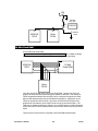
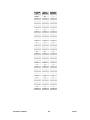
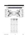
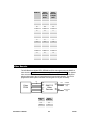
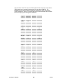
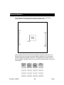
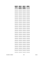
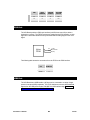
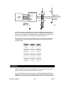
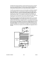
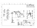
1
2608 Sweetgum Drive
Apex NC 27502
Toll-free: 800-549-9377
International: 919-387-0076
FAX: 919-387-1302
XSV Board V1.0 Manual
How to install and use
your new XSV Board
XSV BOARD V1.0 MANUAL
RELEASE DATE: 5/16/2001
Copyright ©1999-2001 by X Engineering Software Systems Corporation.
All XS-prefix product designations are trademarks of XESS Corp.
All XC-prefix product designations are trademarks of Xilinx.
All rights reserved. No part of this publication may be reproduced, stored in a retrieval
system, or transmitted, in any form or by any means, electronic, mechanical,
photocopying, recording, or otherwise, without the prior written permission of the publisher.
Printed in the United States of America.
XSV BOARD V1.0 MANUAL
RELEASE DATE: 5/16/2001
Table of Contents
Preliminaries........................................................................................................4
Getting Help!.................................................................................................4
Packing List ..................................................................................................4
XSV Overview .....................................................................................................5
XSV Board Features ....................................................................................5
Installation............................................................................................................8
Installing the XSVTOOLs Software .............................................................8
Unpacking the Board ...................................................................................8
Configuring the Jumpers..............................................................................8
Applying Power ............................................................................................8
Connecting to a PC ......................................................................................9
Testing the XSV Board ................................................................................9
Setting the Oscillator Frequency .................................................................9
Programming the Interface ........................................................................10
Downloading Virtex Configuration Bitstreams ..........................................11
Downloading Virtex Configuration Bitstreams to Flash............................12
XSV Circuitry .....................................................................................................13
Programmable logic: XCV50-XCV800 Virtex FPGA and XC95108 CPLD13
100 MHz programmable oscillator ............................................................13
16 Mbit Flash RAM.....................................................................................14
SRAM Banks ..............................................................................................16
Video Decoder............................................................................................17
RAMDAC and VGA Monitor Interface.......................................................18
Stereo Codec..............................................................................................20
Ethernet PHY..............................................................................................20
Expansion Headers....................................................................................23
Pushbuttons and Eight-Position DIP Switch.............................................25
Digit and Bargraph LEDs ...........................................................................26
PS/2 Port.....................................................................................................28
USB Port.....................................................................................................28
Parallel Port ................................................................................................29
Serial Port ...................................................................................................31
Xchecker Interface .....................................................................................32
Power Connectors......................................................................................33
XSV Pin Connections .......................................................................................34
XSV Schematics ...............................................................................................35
3
1
Preliminaries
Getting Help!
Here are some places to get help if you encounter problems:
If you can't get the XS40 Board hardware to work, send an e-mail message describing
your problem to [email protected] or submit a problem report at
http://www.xess.com/reqhelp.html. Our web site also has
answers to frequently-asked-questions,
example designs for the XSV Boards,
application notes,
a place to sign-up for our email forum where you can post questions to other XS
Board users.
If you can't get your XILINX Foundation software tools installed properly, send an email message describing your problem to [email protected] or check their web site
at http://support.xilinx.com.
Packing List
Here is what you should have received in your package:
an XSV Board;
a 6-foot, 25-wire cable with a male DB25 connector at each end;
an XSTOOLs CDROM with software utilities and documentation for using the XSV
Board.
XSV BOARD V1.0 MANUAL
5/16/2001
2
XSV Overview
The XSV Board brings you the power of the XILINX Virtex FPGA embedded in a
framework for processing video and audio signals. The XSV Board has a single Virtex
FPGA from 50K to 800K gates in size. The XSV can digitize PAL, SECAM, or NTSC
video with up to 9-bits of resolution on the red, green, and blue channels and can output
video images through a 110 MHz, 24-bit RAMDAC. The XSV can also process stereo
audio signals with up to 20 bits of resolution and a bandwidth of 50 KHz. Two
independent banks of 512K x 16 SRAM are provided for local buffering of signals and
data.
The XSV Board has a variety of interfaces for communicating with the outside world:
parallel and serial ports, Xchecker cable, a USB port, PS/2 mouse and keyboard port, and
10/100 Ethernet PHY layer interface. There are also two independent expansion ports,
each with 38 general-purpose I/O pins connected directly to the Virtex FPGA.
You can configure the XSV Board through a PC parallel port, serial port, Xchecker cable
or from a bitstream stored in the 16 Mbit Flash RAM. The Flash RAM can also store data
for use by the FPGA after configuration is complete.
XSV Board Features
The XSV Board includes the following resources:
Programmable logic chips:
XILINX Virtex FPGA: Virtex FPGAs from 57 Kgates (XCV50) up to 888 Kgates
(XCV800) in a 240-pin PQFP or HQFP package are compatible with the XSV
Board. The Virtex FPGA is the main repository of programmable logic on the
XSV Board.
XILINX XC95108 CPLD: The CPLD is used to manage the configuration of the
Virtex FPGA via the parallel port, serial port, or Flash RAM. The CPLD also
controls the configuration of the Ethernet PHY chip.
Programmable oscillator that provides a clock signal to the FPGA and CPLD derived
form a 100 MHz base frequency.
16 Mbit Flash RAM that can store multiple configurations or general-purpose data for
the FPGA.
Two independent 512K x 16 SRAM banks used by the FPGA for general-purpose
data storage.
XSV BOARD V1.0 MANUAL
5
5/16/2001
Video decoder that accepts NTSC/PAL/SECAM signals through an RCA jack or Svideo connector and outputs the digitized signal to the FPGA.
RAMDAC with a 256-entry, 24-bit colormap that is used by the FPGA to output video
to a VGA monitor.
Stereo codec that lets the FPGA digitize and generate 0-50 KHz audio signals with up
to 20 bits of resolution.
10BASE-T/100BASE-TX Ethernet PHY that allows the FPGA to access a LAN at up
to 100 Mbps.
Two expansion headers interface the FPGA to external circuitry through 76 generalpurpose I/Os.
Four pushbuttons and one eight-position DIP switch provide general-purpose inputs to
the FPGA and CPLD.
Two LED digits and one LED bargraph let the FPGA and CPLD display status
information.
Mouse/keyboard PS/2 port gives the FPGA access to common PC input devices.
Single USB port provides the FPGA with a serial I/O channel with bandwidths of 1.5 to
12 Mbps.
Parallel/serial port interfaces let the CPLD send and receive data in a parallel or serial
format similar to a PC.
Xchecker cable interface allows downloading and readback of the FPGA
configuration.
ATX power connector or 9 VDC power jack lets the XSV Board receive power from a
standard ATX power supply or a 9 VDC power supply.
The locations of these resources are indicated in the simplified view of the XSV Board
shown below. Each of these resources will be described in the following section.
XSV BOARD V1.0 MANUAL
6
5/16/2001
Parallel Port
9 VDC
Jack
512K x 8
SRAM
16 Mbit Flash
512K x 8
SRAM
Virtex FPGA
(XCV50-800)
512K x 8
SRAM
512K x 8
SRAM
Pushbuttons
Stereo
Output
XSV BOARD V1.0 MANUAL
USB
Port
RJ45
Port
PS/2
Port
7
Expansion Connector
Xchecker
XC95108
CPLD
Ether
Phy
Stereo
Input
RCA S-Video
Jack
Jack
DIP Sw.
ATX Power
Connector
Expansion Connector
Serial
Port
RAM
DAC
VGA
Output
5/16/2001
3
Installation
Installing the XSVTOOLs Software
Run the SETUP.EXE file on the XSVTOOLs CDROM. This will install the utilities and
configuration files for testing and programming your XSV Board.
If you are running Windows NT™ or Win2000™, then you must also install the parallel
port driver using the port95nt.exe installation script on the CDROM.
Unpacking the Board
You should place the XSV Board on a non-conducting surface.
Configuring the Jumpers
1. Place a shunt on jumper J23.
2. Place a shunt on pins 2 and 3 of jumper J31.
3. Place a shunt on pins 2 and 3 of J22.
4. Place a shunt on pins 1 and 2 of J36.
Applying Power
You can supply the XSV Board with power in two ways:
1. Recommended! Attach an ATX PC power supply to connector J11. Remove any
shunts on jumpers J13 and J14. Place a shunt on pins 1 and 2 of jumper J32.
2. Attach a 9 VDC power supply with a 2.1mm, center-positive plug to jack J12. The
power supply must be able to source at least 1.5 A. Place shunts on jumpers J13 and
J14. Place a shunt on pins 1 and 2 of jumper J32.
LED D2 will glow when the power is on.
XSV BOARD V1.0 MANUAL
8
5/16/2001
Connecting to a PC
One DB25 connector on the 6-foot cable should be attached to connector J10 on the XSV
Board and the other end should plug into the parallel port connector of a PC.
Testing the XSV Board
GXSTEST runs your XSV Board through a simple diagnostic routine to validate the
icon placed
operation of the hardware. You start GXSTEST by clicking on the
on the desktop during the XSVTOOLs installation. This brings up the screen shown
below.
Your next step is to select the parallel port that your XS Board is connected to from the
port pulldown list. GXSTEST starts with parallel port LPT1 as the default, but you can also
select LPT2 or LPT3 depending upon the configuration of your PC.
After selecting the parallel port, you select the type of XSV Board you are testing from the
associated pulldown list. Then click on the TEST button to start the testing procedure.
GXSTEST will program the CPLD on the XSV Board and then use it to program the Virtex
FPGA with a test circuit. Status messages will be printed at the bottom of the GXSTEST
window as the testing proceeds. At the end of the test, you will receive a message
informing you whether your XSV Board passed the test or not.
Setting the Oscillator Frequency
The XSV Board has a programmable oscillator which provides a clock signal to the FPGA
and CPLD. The oscillator has an internal 100 MHZ frequency source that is scaled by a
divisor between 1 and 2052 to generate the clock signal for the rest of the XSV Board.
The divisor is stored in non-volatile memory in the oscillator chip so it will be restored each
time power is applied to the XSV Board.
The divisor is set with the GXSSETCLK software utility. You start GXSSETCLK by clicking
on the
icon placed on the desktop during the XSVTOOLs installation. This
brings up the screen shown below.
XSV BOARD V1.0 MANUAL
9
5/16/2001
Your next step is to select the parallel port that your XSV Board is connected to from the
port pulldown list. GXSSETCLK starts with parallel port LPT1 as the default, but you can
also select LPT2 or LPT3 depending upon the configuration of your PC. After selecting
the parallel port, you select "XSV" from the pulldown list of XS Board types.
Next you must enter a divisor between 1 and 2052 into the text box. Once programmed,
the oscillator will output a clock signal generated by dividing its 100 MHz master frequency
by the divisor. The divisor is stored in non-volatile storage in the oscillator chip so you only
need to use GXSSETCLK when you want to change the frequency.
The external clock checkbox is not applicable to the XSV Board because no external clock
is connected to the programmable oscillator chip.
Clicking on the SET button will start the oscillator programming procedure. Status
messages will be printed at the bottom of the GXSSETCLK window as the programming
proceeds. You will also receive instructions on how to set the shunts on the XSV Board
jumpers to place the oscillator into its programming mode. At the end of the programming,
you will receive a message informing you that your XSV Board clock has been set.
Note that GXSSETCLK reprograms the CPLD on the XSV Board in order to access the
programmable oscillator. So you will need to reprogram the CPLD with a parallel port
interface circuit if you want to program the FPGA. (See the next section for details on
this.)
Programming the Interface
The Virtex FPGA is the main repository of programmable logic on the XSV Board. The
CPLD manages the configuration of the FPGA via the parallel port or from the Flash
memory. Therefore, the CPLD must be configured so that it implements the necessary
interface. The CPLD stores its configuration in its internal non-volatile memory so the
interface is restored each time power is applied to the XSV Board (unless the interface
circuit is erased).
The CPLD is enabled for configuration by placing a shunt on jumper J23. The CPLD is
configured with an interface by using the GXSLOAD software utility. You start GXSLOAD
by clicking on the
icon placed on the desktop during the XSVTOOLs installation.
This brings up the screen shown below.
XSV BOARD V1.0 MANUAL
10
5/16/2001
Your next step is to select the parallel port that your XSV Board is connected to using the
Port drop-down list. GXSLOAD starts with parallel port LPT1 as the default, but you can
also select LPT2 or LPT3 depending upon the configuration of your PC.
After setting the parallel port, you can download an .SVF file to the CPLD on the XSV
Board simply by dragging it to the GXSLOAD window. To program the CPLD with the
parallel port interface, drag the dwnldpar.svf file from the XSTOOLS directory. Once you
release the left mouse button and drop the file, GXSLOAD will begin sending it to the XSV
Board through the parallel port connection. During the process, GXSLOAD will display the
name of the file currently being downloaded.
Once the CPLD is programmed with the parallel port interface circuit, you can remove the
shunt from jumper J23 to prevent accidental reprogramming of the CPLD.
Downloading Virtex Configuration Bitstreams
Once the CPLD is programmed with the downloading interface circuit, you can download
bitstreams into the Virtex FPGA using the GXSLOAD utility. Make sure there is a shunt
across pins 2 and 3 of jumper J31. Then drag-and-drop into the GXSLOAD window a
.BIT configuration bitstream for the type of Virtex FPGA on your XSV Board. The
bitstream will pass through the parallel port and CPLD and then into the FPGA. (During
the download process, you will notice a "fluttering" of the bottom segment of the left LED
digit.)
Once the downloading is finished, the .BIT file name is added to the Recent Files window
and the Reload button is enabled. You can download the file to the XSV Board again just
by clicking on the Reload button.
Your XSV Board is now configured with the circuit in your .BIT file.
XSV BOARD V1.0 MANUAL
11
5/16/2001
Downloading Virtex Configuration Bitstreams to Flash
You can also store a bitstream for the FPGA in the 16 Mb Flash RAM on the XSV Board.
Once again, make sure there is a shunt across pins 2 and 3 of jumper J31. Also make
sure that all the DIP switches are in the OFF position. Then just drag-and-drop a .EXO file
containing the bitstream to the GXSLOAD window. GXSLOAD will configure the CPLD
with a circuit that lets it program the Flash RAM. Then GXSLOAD uses the CPLD to
program the Flash with the contents of the .EXO file. Finally, the CPLD is configured with
a circuit that loads the FPGA when power is applied.
Now the Virtex FPGA will be loaded with the circuit you stored in the Flash whenever
power is applied to the XSV Board. You will have to reprogram the CPLD with the
dwnldpar.svf file if you want to reconfigure the FPGA with a .BIT file using the parallel port.
The .EXO file is generated using the Programmer tool in Foundation. The configuration
data should start at address 0 and extend upward to higher addresses. You can also use
the PROMGEN command-line utility to generate the .EXO file like so:
PROMGEN -u 0 FILE.BIT -p exo -s 2048
This creates a .EXO file from the bitstream in FILE.BIT. The -u 0 option causes the first
byte of Flash data to be stored at address 0 and subsequent bytes are stored at
sequentially higher addresses. The -p exo option selects Motorola S record format for
the generated file. The -s 2048 option tells PROMGEN the size of the Flash chip on the
XSV Board (16 Mbits = 2048 KBytes).
XSV BOARD V1.0 MANUAL
12
5/16/2001
4
XSV Circuitry
This section describes the various sections of the XSV Board and shows how the I/O of
the FPGA and CPLD are connected to the rest of the circuitry. The schematics which
follow are less detailed so as to simplify the descriptions. Please refer to the complete
schematics at the end of this document if you need more details.
Programmable logic: XCV50-XCV800 Virtex FPGA and XC95108 CPLD
The XSV Board contains two programmable logic chips:
A XILINX Virtex FPGA in a 240-pin QFP package. Virtex FPGAs from 57 Kgates
(XCV50) up to 888 Kgates (XCV800) are compatible with the XSV Board. The Virtex
FPGA is the main repository of programmable logic on the XSV Board.
A XILINX XC95108 CPLD that is used to manage the configuration of the Virtex
FPGA via the parallel port, serial port, or Flash RAM. The CPLD also controls the
configuration of the Ethernet PHY chip.
100 MHz programmable oscillator
A Dallas DS1075 programmable oscillator
(http://www.dalsemi.com/DocControl/PDFs/1075.pdf) provides a clock signal to both the
FPGA and the CPLD. The DS1075 has a maximum frequency of 100 MHz that is divided
to provide frequencies of 100 MHz, 50 MHz, 33.3 MHz, 25 MHz, ..., 48.7 KHz. The clock
signal is connected to dedicated clock inputs of both the CPLD and FPGA as follows:
DS1075
Output
Virtex
FPGA Pin
XC95108
CPLD Pin
CLK
89
22
To set the divisor value, the DS1075 must be placed in its programming mode. This is
done by pulling the clock output to Vcc on power-up with a shunt across pins 1 and 2 of
jumper J22. Then programming commands to set the divisor can be sent to the DS1075
by either the CPLD or FPGA. The divisor is stored in EEPROM in the DS1075 so it will be
restored whenever power is applied to the XSV Board. The shunt on jumper J22 must be
across pins 2 and 3 to make the oscillator output a clock signal upon power-up.
To get a precise frequency value or to sync the XSV circuitry with an external system, you
can insert an external clock signal through pin 1 of connector J27 and place a shunt
across pins 2 and 3 of jumper J36. This external clock replaces the output from the
DS1075 oscillator.
XSV BOARD V1.0 MANUAL
13
5/16/2001
J22
2
3
1
100 MHz
Prog. Osc.
1
3
22
J36
DS1075
2
89
XC95108
CPLD
J27
Virtex
FPGA
1
External
Clock
16 Mbit Flash RAM
An Intel 28F016S5 Flash RAM
(http://developer.intel.com/design/flcomp/datashts/290597.htm) with 16 Mbits of storage
(2M × 8) is connected to both the Virtex FPGA and XC95108 CPLD as follows:
XC95108
CPLD
8
21
reset
ce
oe
we
rdy
d
0 -7
a
0 -2 0
16 Mbit
Flash RAM
Virtex
FPGA
The CPLD and FPGA both have access to the Flash RAM. Typically, the CPLD will
program the Flash with data passed through the parallel or serial port. If the data is an
FPGA configuration bitstream then the CPLD can be configured to program the FPGA
with the Flash bitstream whenever the XSV Board is powered up. After power-up, the
FPGA can read and/or write the Flash. (Of course, the CPLD and FPGA have to be
programmed such that they do not conflict if both are trying to access the Flash.) The
Flash can be disabled by raising the /CE pin to Vcc in which case the I/O lines connected
to the Flash can be used for general-purpose communication between the FPGA and the
CPLD.
The pins of the FPGA and CPLD connected to the Flash RAM are listed below:
XSV BOARD V1.0 MANUAL
14
5/16/2001
XSV BOARD V1.0 MANUAL
Flash RAM
Pin
Virtex
FPGA Pin
XC95108
CPLD Pin
/RESET
N/A
3
/CE
170
46
/OE
173
42
/WE
131
43
RDY
171
41
D0
177
32
D1
167
33
D2
163
34
D3
156
35
D4
145
36
D5
138
37
D6
134
39
D7
124
40
A0
132
16
A1
133
17
A2
139
18
A3
141
19
A4
144
20
A5
147
23
A6
152
24
A7
154
25
A8
157
27
A9
160
28
A10
162
29
A11
169
30
A12
168
49
A13
161
50
A14
159
52
A15
155
53
A16
153
54
A17
149
55
A18
146
56
A19
142
58
A20
140
59
15
5/16/2001
SRAM Banks
The FPGA has access to two independent banks of SRAM as shown below: Each SRAM
bank is organized as 512K × 16 bits. Each bank is made from two Winbond AS7C4096
SRAMs (ftp://ftp14.ba.best.com/pub/pai/FTP_site/pdf/sram.pdf/as7c34096.pdf). The
FPGA pins connected to the SRAM banks are shown in the accompanying table.
d
8
8
0 -7
4 Mbit
SRAM
ce
oe
we
d
0 -7
ce
oe
we
19
19
a
0 -1 8
a
a
0 -1 8
ce
oe
we
ce
oe
we
a
0 -1 8
4 Mbit
SRAM
Virtex
FPGA
0 -1 8
4 Mbit
SRAM
d
8
8
0 -7
XSV BOARD V1.0 MANUAL
SRAM Pin
Virtex
FPGA Pin
to Left
Bank
Virtex
FPGA Pin
to Right
Bank
/CE
186
109
/OE
228
95
/WE
201
68
D0
202
70
D1
203
71
D2
205
72
D3
206
73
D4
207
74
D5
208
78
D6
209
79
D7
215
80
D8
216
81
D9
217
82
D10
218
84
D11
220
85
D12
221
86
D13
222
87
D14
223
93
D15
224
94
16
d
4 Mbit
SRAM
0 -7
5/16/2001
SRAM Pin
Virtex
FPGA Pin
to Left
Bank
Virtex
FPGA Pin
to Right
Bank
A0
200
67
A1
199
66
A2
195
65
A3
194
64
A4
193
63
A5
192
57
A6
191
56
A7
189
55
A8
188
54
A9
187
53
A10
238
108
A11
237
107
A12
236
103
A13
235
102
A14
234
101
A15
232
100
A16
231
99
A17
230
97
A18
229
96
Video Decoder
The XSV Board can digitize NTSC, SECAM, and PAL video signals using the SAA7113
video decoder (http://www-us.semiconductors.philips.com/pip/SAA7113H). The digitized
video arrives at the FPGA over the VPO bus. The arrival of video data is synchronized
with the rising edge of the LLC (line-locked clock) from the video decoder. The FPGA
2
programs the video options of the SAA7113 using the I C bus (SCL and SDA).
8
vpo
rts0
rts1
rtco
llc
scl
sda
0 -7
Virtex
FPGA
SAA7113
Pin
XSV BOARD V1.0 MANUAL
SAA7113
Video
Decoder
ai11
ai12
ai21
ai22
S-Video
Connector
(J8)
chroma
luma
cvbs
RCA Jack
(J9)
Virtex
FPGA Pin
LLC
92
RTS0
111
RTS1
110
17
5/16/2001
SAA7113
Pin
Virtex
FPGA Pin
RTCO
113
VPO0
116
VPO1
117
VPO2
118
VPO3
125
VPO4
126
VPO5
127
VPO6
128
VPO7
130
SCL
114
SDA
115
RAMDAC and VGA Monitor Interface
The FPGA can generate a video signal for display on a VGA monitor either directly or
using a BT481A RAMDAC
(http://www.erc.msstate.edu/~reese/EE4993/data_sheets/btl481a_c.pdf) depending upon
the arrangement of the shunts on jumpers J5, J6, and J7.
vsync
hsync
p
p
p
p
p
p
5
4
3
2
r
1
0
0
8
p
Virtex
FPGA
0 -7
blank
pixelclk
rd
wr
rs
d
0 -2
8
red
BT481A
RAMDAC
green
blue
r
1
g
0
g
1
J5
b
0
b
1
VGA
Connector
(J4)
red
J6
green
J7
blue
0 -7
When the FPGA is directly generating VGA signals, the lower six bits of the P bus provide
two-bits of red, green, and blue color information to a simple resistor-ladder DAC. The
outputs of the DAC are sent to a VGA monitor along with the horizontal and vertical sync
pulses (/HSYNC, /VSYNC) from the FPGA.
When the RAMDAC generates the VGA color signals, then the FPGA uses the full eightbit P bus to pass the index of the color for the current pixel. The index is used to lookup
the 24-bit color value (eight bits for the red, green, and blue components) stored in the
XSV BOARD V1.0 MANUAL
18
5/16/2001
256-entry colormap of the RAMDAC chip. The transfers over the P bus are synchronized
with the PIXELCLK generated by the FPGA. The FPGA lowers the /BLANK signal when
the pixels fall outside the desired visible area of the monitor screen.
The colormap of the RAMDAC is initialized by the FPGA using the D bus along with the
RS, /WR, and /RD signals. The 24-bit colormap entries are passed in groups of three
bytes over the eight-bit D bus synchronized by the /WR signal. The register-select signals
(RS0, RS1, RS2) select the staging register for writing the colormap. The contents of the
staging register are written into the colormap after the last byte of color information arrives
over the D bus, and then the internal colormap address is incremented to point to the next
entry.
The shunt placement to enable the FPGA to generate VGA signals directly or through the
RAMDAC is shown below.
J7
J6
J5
J7
Direct VGA
Shunt Setting
J6
J5
RAMDAC
Shunt Setting
The pin assignments for the connection of the FPGA to the VGA signal generation circuitry
are shown below. Note that the FPGA shares some connections between the RAMDAC
and the chip which interfaces to the Ethernet (LXT970A). The RAMDAC pins are used to
load the colormap and should not be active except during system initialization. The other
connections are used for Ethernet data transmission and reception and are usually only
active after system initialization.
Direct
VGA Pin
XSV BOARD V1.0 MANUAL
RAMDAC
Pin
Virtex
FPGA Pin
PIXELCLK
52
/HSYNC
/HSYNC
48
/VSYNC
/VSYNC
49
/BLANK
50
RED0
P0
70
RED1
P1
71
GREEN0
P2
72
GREEN1
P3
73
BLUE0
P4
74
BLUE1
P5
78
P6
79
LXT970A
Function
P7
80
/RD
47
/WR
46
RS0
31
TXD4
RS1
28
RX_ER
RS2
26
RX_DV
D0
42
TXD0
19
5/16/2001
Direct
VGA Pin
RAMDAC
Pin
Virtex
FPGA Pin
LXT970A
Function
D1
41
TXD1
D2
40
TXD2
D3
39
TXD3
D4
38
RXD0
D5
36
RXD1
D6
35
RXD2
D7
34
RXD3
Stereo Codec
The XSV Board has an AK4520A stereo codec
(http://www.akm.com/ProductPages/ak4520a.html) that accepts two analog input
channels from jack J1, digitizes the analog values, and sends the digital values to the
FPGA as a serial bit stream. The codec also accepts a serial bit stream from the XS
Board and converts it into two analog output signals, which exit the XSV Board through
jack J2. The serial bit streams are synchronized with a clock from the FPGA that enters
the codec on SCLK signal. The FPGA uses the LRCK signal to select the left or right
channel as the source/destination of the serial data. The master clock from the FPGA
(MCLK) synchronizes all the internal operations of the codec.
Virtex
FPGA
mclk
in
le ft
lrck
in
r ig h t
sclk
sdin
AK4520A
Codec
sdout
Stereo Jack
(J1)
out
le f t
out
rig h t
Amp
Stereo Jack
(J2)
The FPGA pins which connect to the codec are as follows:
Stereo
Codec Pin
Virtex
FPGA Pin
MCLK
3
LRCK
4
SCLK
5
SDIN
6
SDOUT
7
Ethernet PHY
The XSV Board interfaces to an Ethernet LAN at 10 or 100 Mbps. The LXT970A Ethernet
PHY chip (http://128.11.21.45/scripts/mardev/product/lxt970.asp ) connects to both the
FPGA and the CPLD. The FPGA acts as a MAC (media access controller) and manages
the transfer of data packets to and from the PHY chip, while the CPLD controls the
configuration pins that determine the operational mode of the PHY chip.
XSV BOARD V1.0 MANUAL
20
5/16/2001
tx_err
tx_clk
tx_en
txd
rx_er
rx_clk
rx_dv
rxd
col
crs
trste
fds/mdint
mdio
mdc
4
Virtex
FPGA
4
tpop
tpon
tpip
0 -4
4
2
tpin
transformer
0 -4
RJ45
Connector
(J3)
LXT970A
Ethernet
PHY
mf
cfg
0 -4
0 -1
XC95108
CPLD
mddis
fde
reset
pwrdwn
leds
ledr
ledt
ledl
ledc
The FPGA enables the transmitter with TX_EN and sends bits on TXD4-0 in sync with the
transmit clock (TX_CLK) generated by the PHY chip. The PHY chip is alerted to
transmission errors that occur in the MAC when the TX_ERR signal is asserted. The
FPGA also receives an indication when valid data has been received (RX_DV) and the
data (RXD0-4) in sync with the receiver clock (RX_CLK) from the PHY chip. Any reception
errors are indicated to the FPGA via the RX_ER signal. The CRS signal indicates when
the receiver is non-idle. The COL signal is asserted when data collides on the Ethernet.
The FPGA can disable the interface to the PHY chip by asserting the tristate control
(TRSTE). Otherwise, the FPGA passes management information to and from the PHY
chip over the serial data line (MDIO) in sync with a clock (MDC). the FPGA can be alerted
to changes in PHY chip status by the FDS/MDINT interrupt line.
The CPLD sets the static values on pins which control the configuration of the PHY chip.
Pins MF0-4 set the modes for auto-negotiation, repeating, symbol transmission,
scrambling, etc. Likewise, the configurations signals (CFG0-1) select the 10 Mbps or 100
Mbps operating speed of the PHY chip. MDDIS enables/disables the management
information interface. FDE selects either full-duplex or half-duplex communication mode.
The reset (/RESET) and power-down (PWRDWN) signals do exactly what they say.
The CPLD also gets receives the status outputs from the PHY chip that normally drive
LEDs. The outputs are active-low and indicate when 100 Mbps operation is selected
(/LEDS), the receiver is active (/LEDR), the transmitter is active (/LEDT), the link is active
(/LEDL), and a collision is detected (/LEDC). The CPLD can relay these signals to the
LEDs on the XSV Board if you wish to display the Ethernet status.
XSV BOARD V1.0 MANUAL
21
5/16/2001
The connections of the PHY chip to the FPGA and CPLD are listed below. Note that the
FPGA shares some connections between the PHY chip and the RAMDAC. The
RAMDAC pins are used to load the colormap and should not be active except during
system initialization. The PHY connections are used for data transmission and reception
and are usually only active after system initialization.
XSV BOARD V1.0 MANUAL
LXT970A
Pin
Virtex
FPGA Pin
COL
23
CRS
21
XC95108
CPLD Pin
RAMDAC
TRSTE
24
TX_CLK
210
TX_EN
25
TX_ER
27
TXD0
42
D0
TXD1
41
D1
TXD2
40
D2
TXD3
39
D3
RS0
TXD4
31
RX_CLK
213
RX_DV
26
RS2
RX_ER
28
RS1
RXD0
38
D4
RXD1
36
D5
RXD2
35
D6
RXD3
34
D7
RXD4
33
FDS/MDINT
18
MDC
19
MDIO
20
MDDIS
94
MF0
91
MF1
90
MF2
89
MF3
87
MF4
86
CFG0
93
CFG1
2
FDE
92
/RESET
3
/LEDS
1
/LEDR
95
/LEDT
96
/LEDL
97
/LEDC
99
22
5/16/2001
Expansion Headers
The XSV Board has two 50-pin headers (J25 and J26) which connect the FPGA to
external systems. The arrangement of the headers is shown below:
50
49
2
1
2
1
J26
Virtex
FPGA
50
49
U18
J25
The connections between the FPGA and the expansion headers are listed below. The
FPGA pins which connect to the left and right expansion headers are also connected to
the left and right banks of SRAM, respectively. The SRAM bank chip-enable should be
raised to disable the SRAMs on that side if the associated expansion header is being used
for external I/O.
Expansion
Connector
Pin
Virtex
FPGA Pin
to Left
Connector
Virtex
FPGA Pin
to Right
Connector
SRAM
Function
1
186
109
/CE
2
187
53
3
XSV BOARD V1.0 MANUAL
A9
+5V
4
188
54
A8
5
189
55
A7
6
191
56
A6
23
5/16/2001
Expansion
Connector
Pin
Virtex
FPGA Pin
to Left
Connector
Virtex
FPGA Pin
to Right
Connector
8
192
57
A5
9
193
63
A4
10
194
64
A3
7
GND
11
+5
12
195
65
A2
13
199
66
A1
14
200
67
A0
16
201
68
/WE
17
202
70
D0
18
203
71
D1
20
205
72
D2
21
206
73
D3
22
207
74
15
GND
19
+5
23
D4
GND
24
208
78
D5
25
209
79
D6
26
215
80
D7
28
216
81
D8
29
217
82
D9
30
218
84
27
+3.3
31
D10
GND
32
220
85
D11
33
221
86
D12
34
222
87
35
D13
+3.3
36
223
93
D14
37
224
94
D15
38
228
95
39
/OE
GND
40
229
96
A18
41
230
97
A17
42
231
99
A16
44
232
100
A15
45
234
101
A14
46
235
102
43
+3.3
47
XSV BOARD V1.0 MANUAL
SRAM
Function
A13
GND
48
236
103
A12
49
237
107
A11
50
238
108
A10
24
5/16/2001
Pushbuttons and Eight-Position DIP Switch
The XSV Board has a bank of eight DIP switches and four pushbuttons that are
accessible from the FPGA. The CPLD is also connected to the DIP switches and one of
the pushbuttons. When pressed, each pushbutton pulls the connected pin of the FPGA
and CPLD to ground. Otherwise, the pin is pulled high through a resistor. Likewise, each
DIP switch pulls the connected pin of the FPGA or CPLD to ground when it is closed or
ON. When the DIP switch is open or OFF, the pin is pulled high through a resistor.
When not being used, the DIP switches should be left in the open or OFF
configuration so the pins of the FPGA and CPLD are not tied to ground and can
freely move between logic low and high levels.
External
Clock
DIP
Switch
(SW6)
SW4
SW3
SW2
SW1
XC95108
CPLD
Virtex
FPGA
The table below lists the connections from the FPGA and CPLD to the switches. The DIP
switches also share the same pins as the uppermost eight bits of the Flash RAM address
bus. If the Flash RAM is programmed with several FPGA bitstreams, then the DIP switch
can be used to select a particular bitstreams which will be loaded into the FPGA by the
CPLD on power-up.
XSV BOARD V1.0 MANUAL
25
5/16/2001
Switch
Virtex
FPGA Pin
XC95108
CPLD Pin
Flash RAM
Function
SW1
174
SW2
175
SW3
176
SW4
185
7
DIPSW1
161
50
A13
DIPSW2
159
52
A14
DIPSW3
155
53
A15
DIPSW4
153
54
A16
DIPSW5
149
55
A17
DIPSW6
146
56
A18
DIPSW7
142
58
A19
DIPSW8
140
59
A20
Digit and Bargraph LEDs
The XSV Board has a 10-segment bargraph LED and two more 7-segment LED digits for
use by the FPGA and CPLD. All of these LEDs are active-high meaning that an LED
segment will glow when a logic-high is applied to it.
The table below lists the connections from the FPGA and CPLD to the LEDs. The LEDs
also share the same pins as the uppermost eight bits of the Flash RAM address bus. If
the Flash RAM is programmed with several FPGA bitstreams, then the DIP switch can be
used to select a particular bitstreams which will be loaded into the FPGA by the CPLD.
XSV BOARD V1.0 MANUAL
26
5/16/2001
S6
8
8
S5
S4
S2 S3 S1
S0
S6
S5
S4
S2 S3 S1
S0
7
7
7 10
Bargraph
Right Digit
Left Digit
XC95108
CPLD
XSV BOARD V1.0 MANUAL
7
10
Virtex
FPGA
LED
Virtex
FPGA Pin
XC95108
CPLD Pin
Flash RAM
Function
SL0
177
32
D0
SL1
167
33
D1
SL2
163
34
D2
SL3
156
35
D3
SL4
145
36
D4
SL5
138
37
D5
SL6
134
39
D6
SR0
124
40
D7
SR1
132
16
A0
SR2
133
17
A1
SR3
139
18
A2
SR4
141
19
A3
SR5
144
20
A4
SR6
147
23
A5
B0
152
24
A6
B1
154
25
A7
B2
157
27
A8
B3
160
28
A9
B4
162
29
A10
B5
169
30
A11
B6
168
49
A12
27
5/16/2001
LED
Virtex
FPGA Pin
XC95108
CPLD Pin
Flash RAM
Function
B7
173
42
/OE
B8
131
43
/WE
B9
171
41
RDY
PS/2 Port
The XSV Board provides a PS/2-style interface (mini-DIN connector J20) to either a
keyboard or a mouse. The FPGA receives two signals from the PS/2 interface: a clock
signal and a serial data stream that is synchronized with the falling edges on the clock
signal.
Virtex
FPGA
clk
data
PS/2
Connector
(J20)
The following table shows the connections from the FPGA to the PS/2 interface.
PS/2 Port
Pin
Virtex
FPGA Pin
CLK
13
DATA
17
USB Port
The XSV Board has a USB interface (J35) that can be connected to a variety of highspeed or low-speed USB peripherals. The FPGA interfaces to the two differential data
signals from the USB port through a PDIUSBP11A USB interface chip (http://wwwus.semiconductors.philips.com/pip/PDIUSBP11A_2).
XSV BOARD V1.0 MANUAL
28
5/16/2001
PDIUSBP11A
/OE
VPO
VMO/FSEO
RCV
VP
VM
SUSPND
SPEED
MODE
Virtex
FPGA
J37
3
low
speed
D-
1
3
2
J18
J16
high
speed
V
c c
DD+
D+
J34
J33
1
high 2 low
speed speed
J19
The USB port is set to high (12 Mbps) or low speed (1.5 Mbps) by shunts on jumpers J18
and J37. A 15K load can be placed on the D+ and D- USB signals by placing shunts
across jumpers J33 and J34. If the USB peripheral connected to the port needs to draw
power from the XSV Board, then a shunt should be placed on jumper J16.
The connections of the FPGA to the USB interface chip are listed below. Note that the
FPGA shares some of its pins between the USB interface, the PS/2 interface and one
pushbutton switch.
PDIUSB11A
Pin
Virtex
FPGA Pin
Other
Functions
/OE
12
VPO
13
PS/2 CLK
VMO/FSEO
17
PS/2 DATA
RCV
11
VP
10
VM
9
SUSPND
176
SW3
Parallel Port
The CPLD handles the interface to the parallel port. The seventeen active lines of the
parallel port connect to general-purpose I/O pins on the CPLD.
Four of the parallel port lines also connect to the JTAG pins through which the CPLD is
programmed. The TCK signal clocks configuration data in through the TDI pin while the
TMS signal steers the actions of the programming state machine. The TDO pin outputs
XSV BOARD V1.0 MANUAL
29
5/16/2001
USB
Connector
(J35)
information back through the parallel port. Removing the shunt from jumper J23 isolates
the TCK pin from the parallel port so the CPLD will not be inadvertently reprogrammed
during routine parallel port operations. The series resistor prevents the TDO output from
interfering with the general-purpose I/O pin during routine parallel port operations.
The CPLD can be programmed to act as an interface between the FPGA and the parallel
port (the dwnldpar.svf file is an example of such an interface). Schmitt-trigger inverters
can be inserted into the d0, d1, and c1 signal lines by placing shunts on pins 2 and 3 of
jumpers J29, J30, and J31, respectively. Along with the parallel port interface circuitry in
the CPLD, these inverters make the XSV Board compatible with the GXSPORT and
GXSLOAD software utilities. If your application requires direct access to these signal
lines, then you can move the shunts on one or more of these jumpers to pins 1 and 2. But
GXSLOAD will no longer work if you remove the inverter from the c1 signal line.
Be careful if you program the CPLD with outputs that drive the c1, c2, c3, and
s7 pins of the parallel port. These parallel port pins are also connected to the JTAG
pins of the CPLD and are used to reprogram the CPLD. If you program the CPLD to drive
these pins, then it will permanently prevent the PC from reprogramming the CPLD. As an
ultra-conservative rule-of-thumb, you should never configure CPLD pins 63, 71,
73, or 78 as outputs. If you must use these pins as outputs, then place them in a high-
impedance mode whenever the Virtex FPGA is unconfigured (i.e., the Virtex DONE pin is
at logic 0). This will allow you to regain control of the parallel port by toggling the power to
the board.
J29
3
2
d
0
1
J30
3
2
d
1
1
d
d
d
d
d
d
s
s
s
s
s
c
2
3
4
5
6
7
3
Parallel Port
Connector
(J10)
4
5
XC95108
CPLD
6
7
0
J31
3
2
1
1
c
c
2
3
J23
tdi
tms
tck
tdo
XSV BOARD V1.0 MANUAL
c
30
5/16/2001
The table below lists the connections from the parallel port to the general-purpose I/O pins
of the CPLD:
Parallel
Port Pin
XC95108
CPLD Pin
1 (C0)
79
2 (D0)
77
3 (D1)
74
4 (D2)
72
5 (D3)
70
6 (D4)
68
7 (D5)
67
8 (D6)
66
9 (D7)
65
10 (S6)
64
11 (S7)
63
12 (S5)
61
13 (S4)
60
14 (C1)
78
15 (S3)
76
16 (C2)
73
17 (C3)
71
Serial Port
The CPLD handles the interface to the serial port. The four active lines of the serial port
connect to general-purpose I/O pins on the CPLD as follows.
XSV BOARD V1.0 MANUAL
Serial Port
Pin
XC95108
CPLD Pin
RTS
82
TD
81
CTS
85
RD
80
31
5/16/2001
MAX232A
rd
cts
XC95108
CPLD
td
Serial Port
Connector
(J28)
rts
level
shifters
Xchecker Interface
Header J21 provides an interface between the FPGA and an Xchecker cable. The
Xchecker cable can be used to perform configuration and readback operations on the
FPGA. To prevent interference, the shunt should be removed from jumper J36 to
disconnect the DS1075 and any external clocks from the clock input through the Xchecker
cable (CLKI). You must also make sure the CPLD pins in the table below are in a highimpedance state. In addition, the CPLD should place a high logic level on the chip-enable
pin of the Flash RAM to prevent the LSB of its data pins from interfering with the DIN pin of
the Xchecker interface.
Xchecker Pin
XSV BOARD V1.0 MANUAL
Virtex FPGA Pin
CPLD Pin
1 – VCC (+5V)
N/A
N/A
2 – RT
132
16
3 – GND
N/A
N/A
4 – RD
133
17
6 – TRIG
139
18
7 – CCLK
179
12
9 – DONE
120
10
10 – TDI
167
33
11 – DIN
177
32
12 – TCK
239
4
13 – PROGRAM
122
11
14 – TMS
156
35
15 – INIT
123
9
16 – CLKI
89
22
17 – RST
144
20
18 – CLKO
141
19
32
5/16/2001
If you also want to access the JTAG port of the FPGA, all the requisite pins are already
connected to the Xchecker interface except for TDO. The TDO pin of the FPGA connects
to pin 34 of the CPLD, so you must route the signal through the CPLD and onto the RD
pin of the Xchecker interface (which the Xchecker uses for TDO). You must also make
sure that pins 133 and 163 on the FPGA are tristated in your design or else they will
override TDO.
XC95108
CPLD
17
34
300 Ω
133 181
4-RD
163
Virtex
FPGA
You can get a complete Xchecker interface for the CPLD from
http://www.xess.com/appnotes/an-050101-xsvxchk.pdf.
Power Connectors
A standard ATX PC power supply can be connected to the XSV Board through connector
J11. The connector is keyed so power cannot be applied with the wrong polarity. The
shunts should be removed from jumpers J13 and J14 to prevent the 9 VDC converter
circuitry from interfering with the ATX power supply. We recommend using the ATX
power supply due to its stability and power capacity.
The XSV Board can also be powered from a 9 VDC power supply through jack J12. The
power supply must have a 2.1mm, center-positive plug. Two voltage regulators will
generate the 5V and 3.3V voltages for the other XSV Board components. Shunts should
be placed on jumpers J13 and J14 to connect the outputs from the voltage regulators to
the rest of the XSV Board. We do not recommend the 9 VDC power input for general use!
The 2.5V for the Virtex FPGA core logic can be generated on the XSV Board or supplied
from an external source. Placing a shunt across pins 1 and 2 of jumper J32 will use the
on-board regulator to generate the 2.5V from the 5V supply. You can inject 2.5V from an
external source by attaching the positive terminal to pin 2 of jumper J32 and ground to pin
3.
XSV BOARD V1.0 MANUAL
33
5/16/2001
A
XSV Pin
Connections
The following tables list the pin numbers of the Virtex FPGA and the XC95108 CPLD
along with the pin names of the other chips that they connect to. These connections
correspond with the pin assignments in the user-constraint files VIRTEX.UCF and
CPLD.UCF.
XSV BOARD V1.0 MANUAL
34
5/16/2001
Connections Between the Virtex FPGA and the Other XSV Board Components
Virtex FPGA
1
GND
2
TMS
3
4
5
6
7
8
GND
9
10
11
12
13
14
GND
15
VCCO
16
VCCINT
17
18
19
20
21
22
GND
23
24
25
26
27
28
29
GND
30
VCCO
31
32
VCCINT
33
34
35
36
37
GND
38
39
40
41
42
43
VCCINT
44
VCCO
45
GND
XC95108
CPLD
35
LEDs
S3 (left)
Switches
Flash
RAM
Ethernet
Video
Decoder RAMDAC
Codec
RAM
PS/2
USB
D3
Parallel
Port
Serial
Port
Prog.
Osc.
Xchecker
TMS
MCLK
LRCK
SCLK
SDIN
SDOUT
FDS/MDINT
MDC
MDIO
CRS
COL
TRSTE
TxEN
RxDV
TxERR
RxERR
RS2
RS1
TxD4
RS0
RxD4
RxD3
RxD2
RxD1
D7
D6
D5
RxD0
TxD3
TxD2
TxD1
TxD0
D4
D3
D2
D1
D0
CLK
VM
VP
RCV
/OE
VPO
DATA
VMO
Connections Between the Virtex FPGA and the Other XSV Board Components
Virtex FPGA
46
47
48
49
50
51
GND
52
53
54
55
56
57
58
M1
59
GND
60
M0
61
VCCO
62
M2
63
64
65
66
67
68
69
GND
70
71
72
73
74
75
GND
76
VCCO
77
VCCINT
78
79
80
81
82
83
GND
84
85
86
87
88
VCCINT
89
PGCK
90
VCCO
XC95108
CPLD
LEDs
Switches
Flash
RAM
Ethernet
Video
Decoder RAMDAC
/WR
/RD
/HSYNC
/VSYNC
/BLANK
Codec
RAM
PS/2
USB
Parallel
Port
Serial
Port
Prog.
Osc.
Xchecker
PIXELCLK
A9 (right)
A8 (right)
A7 (right)
A6 (right)
A5 (right)
14
13
15
A4 (right)
A3 (right)
A2 (right)
A1 (right)
A0 (right)
/WE (right)
P0
P1
P2
P3
P4
D0 (right)
D1 (right)
D2 (right)
D3 (right)
D4 (right)
P5
P6
P7
D5 (right)
D6 (right)
D7 (right)
D8 (right)
D9 (right)
D10 (right)
D11 (right)
D12 (right)
D13 (right)
22
CLK
CLKI
Connections Between the Virtex FPGA and the Other XSV Board Components
Virtex FPGA
91
GND
92
PGCK
93
94
95
96
97
98
GND
99
100
101
102
103
104
VCCINT
105
VCCO
106
GND
107
108
109
110
111
112
GND
113
114
115
116
117
118
119
GND
120
DONE
121
VCCO
122
/PROG
123
/INIT
124
D7
125
126
127
128
129
GND
130
131
132
133
134
D6
135
GND
XC95108
CPLD
LEDs
Switches
Flash
RAM
Ethernet
Video
Decoder RAMDAC
Codec
RAM
PS/2
USB
Parallel
Port
Serial
Port
Prog.
Osc.
Xchecker
LLCK
D14 (right)
D15 (right)
/OE (right)
A18 (right)
A17 (right)
A16 (right)
A15 (right)
A14 (right)
A13 (right)
A12 (right)
A11 (right)
A10 (right)
/CE (right)
RTS1
RTS0
RTC0
SCL
SDA
VPO0
VPO1
VPO2
10
DONE
11
9
40
/PROGRAM
/INIT
S0 (right)
D7
VPO3
VPO4
VPO5
VPO6
VPO7
43
16
17
39
BAR8
S1 (right)
S2 (right)
S6 (left)
/WE
A0
A1
D6
RT
RD
Connections Between the Virtex FPGA and the Other XSV Board Components
XC95108
CPLD
Virtex FPGA
136
VCCO
137
VCCINT
138
D5
139
140
141
142
143
GND
144
145
D4
146
147
148
VCCINT
149
150
VCCO
151
GND
152
153
154
155
156
D3
157
158
GND
159
160
161
162
163
D2
164
VCCINT
165
VCCO
166
GND
167
D1
168
169
170
171
172
GND
173
174
175
176
177
D0/DIN
BUSY/DOUT
178
179
CCLK
180
VCCO
37
18
59
19
58
20
36
56
23
LEDs
S5 (left)
S3 (right)
DIPSW8
S4 (right)
DIPSW7
S5 (right)
S4 (left)
DIPSW6
S6 (right)
55
24
54
25
53
35
27
52
28
50
29
34
Switches
DIPSW5
BAR0
DIPSW4
BAR1
DIPSW3
S3 (left)
BAR2
DIPSW2
BAR3
DIPSW1
BAR4
S2 (left)
33
49
30
46
41
S1 (left)
BAR6
BAR5
42
BAR7
Flash
RAM
Codec
RAM
PS/2
USB
Parallel
Port
Serial
Port
Prog.
Osc.
Xchecker
TRIG
CLKO
A4
D4
A18
A5
RST
A17
A6
A16
A7
A15
D3
A8
TMS
A14
A9
A13
A10
D2
D1
A12
A11
/CE
RDY
BAR9
S0 (left)
Video
Decoder RAMDAC
D5
A2
A20
A3
A19
TDI
/OE
SW1
SW2
SW3
32
6
12
Ethernet
SUSPND
D0
DIN
CCLK
Connections Between the Virtex FPGA and the Other XSV Board Components
Virtex FPGA
181
TDO
182
GND
183
TDI
184
/CS
185
/WR
186
187
188
189
190
GND
191
192
193
194
195
196
GND
197
VCCO
198
VCCINT
199
200
201
202
203
204
GND
205
206
207
208
209
210
PGCK
211
GND
212
VCCO
213
PGCK
214
VCCINT
215
216
217
218
219
GND
220
221
222
223
224
225
VCCINT
XC95108
CPLD
LEDs
34
S2 (left)
33
8
7
Switches
S1 (left)
Flash
RAM
D2
Ethernet
Video
Decoder RAMDAC
Codec
RAM
D1
PS/2
USB
Parallel
Port
Serial
Port
Prog.
Osc.
Xchecker
TDI
SW4
/CE (left)
A9 (left)
A8 (left)
A7 (left)
A6 (left)
A5 (left)
A4 (left)
A3 (left)
A2 (left)
A1 (left)
A0 (left)
/WE (left)
D0 (left)
D1 (left)
D2 (left)
D3 (left)
D4 (left)
D5 (left)
D6 (left)
TxCLK
RxCLK
D7 (left)
D8 (left)
D9 (left)
D10 (left)
D11 (left)
D12 (left)
D13 (left)
D14 (left)
D15 (left)
Connections Between the Virtex FPGA and the Other XSV Board Components
Virtex FPGA
226
VCCO
227
GND
228
229
230
231
232
233
GND
234
235
236
237
238
239
TCK
240
VCCO
XC95108
CPLD
LEDs
Switches
Flash
RAM
Ethernet
Video
Decoder RAMDAC
Codec
RAM
PS/2
USB
Parallel
Port
Serial
Port
Prog.
Osc.
Xchecker
/OE (left)
A18 (left)
A17 (left)
A16 (left)
A15 (left)
A14 (left)
A13 (left)
A12 (left)
A11 (left)
A10 (left)
4
TCK
Connections Between the XC95108 CPLD and the Other XSV Board Components
XC95108 CPLD
1
2
3
4
5
VCCINT
6
7
8
9
10
11
12
13
14
15
16
17
18
19
20
21
GND
22
PGCK
23
PGCK
24
25
26
VCCO
27
PGCK
28
29
30
31
GND
32
33
34
35
36
37
38
VCCO
39
40
41
42
Virtex
FPGA
LEDs
Switches
Flash
RAM
/RESET
Video
Ethernet Decoder RAMDAC
/LEDS
CFG1
/RESET CE
Codec
RAM
PS/2
USB
Parallel
Port
Serial
Port
Prog.
Osc.
239
TCK
178
185
184
123
120
122
179
60
58
62
132
133
139
141
144
S1 (right)
S2 (right)
S3 (right)
S4 (right)
S5 (right)
A0
A1
A2
A3
A4
89
147
152
154
S6 (right)
BAR0
BAR1
A5
A6
A7
157
160
162
169
BAR2
BAR3
BAR4
BAR5
A8
A9
A10
A11
S0 (left)
S1 (left)
S2 (left)
S3 (left)
S4 (left)
S5 (left)
D0
D1
D2
D3
D4
D5
S6 (left)
S0 (right)
BAR9
BAR7
D6
D7
RDY
/OE
177
167,183
163,181
156,2
145
138
134
124
171
173
Xchecker
SW4
/INIT
DONE
/PROGRAM
CCLK
RT
RD
TRIG
CLKO
CLK
CLKI
DIN
TDI
TMS
Connections Between the XC95108 CPLD and the Other XSV Board Components
XC95108 CPLD
43
44
GND
45
TDI
46
47
TMS
48
TCK
49
50
51
VCCO
52
53
54
55
56
57
VCCINT
58
59
60
61
62
GND
63
64
65
66
67
68
69
GND
70
71
72
73
74
75
GND
76
77
78
79
80
81
82
83
TDO
84
GND
Virtex
FPGA
131
LEDs
BAR8
Switches
Flash
RAM
/WE
Ethernet
Video
Decoder RAMDAC
Codec
RAM
PS/2
USB
Parallel
Port
Serial
Port
C3
170
/CE
C2
C1
168
161
BAR6
DIPSW1
A12
A13
159
155
153
149
146
DIPSW2
DIPSW3
DIPSW4
DIPSW5
DIPSW6
A14
A15
A16
A17
A18
142
140
DIPSW7
DIPSW8
A19
A20
S4
S5
S7
S6
D7
D6
D5
D4
D3
C3
D2
C2
D1
S3
D0
C1
C0
RxD
TxD
RTS
S7
Prog.
Osc.
Xchecker
Connections Between the XC95108 CPLD and the Other XSV Board Components
XC95108 CPLD
85
86
87
88
VCCO
89
90
91
92
93
94
95
96
97
98
VCCINT
99
100
GND
Virtex
FPGA
LEDs
Switches
Flash
RAM
Ethernet
MF4
MF3
MF2
MF1
MF0
FDE
CFG0
MDDIS
/LEDR
/LEDT
/LEDL
/LEDC
Video
Decoder RAMDAC
Codec
RAM
PS/2
USB
Parallel
Port
Serial
Port
CTS
Prog.
Osc.
Xchecker
B
XSV Schematics
The following pages show the detailed schematics for the XSV Board.
XSV BOARD V1.0 MANUAL
35
5/16/2001