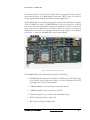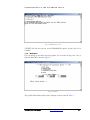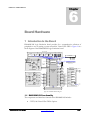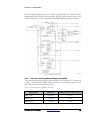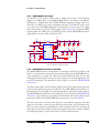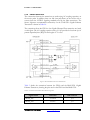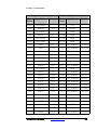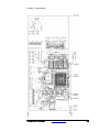
1
THE DINI GROUP
LOGIC Emulation Source
User Guide
DN6000K10S
LOGIC EMULATION SOURCE
DN6000K10S User Manual Version 1.2
© The Dini Group
1010 Pearl Street • Suite 6
La Jolla, CA92037
Phone 858.454.3419 • Fax 858.454.1279
[email protected]
www.dinigroup.com
Table of Contents
ABOUT THIS MANUAL ......................................................................................................................................................................................................... 1
1
2
3
MANUAL CONTENTS.................................................................................................................................................................................................... 1
ADDITIONAL RESOURCES ............................................................................................................................................................................................ 1
CONVENTIONS ............................................................................................................................................................................................................. 2
3.1
Typographical ......................................................................................................................................................................................................... 2
3.2
Online Document..................................................................................................................................................................................................... 3
4
RELEVANT INFORMATION ........................................................................................................................................................................................... 4
GETTING STARTED .............................................................................................................................................................................................................. 6
1
2
3
PRECAUTION ................................................................................................................................................................................................................ 6
THE DN6000K10S LOGIC EMULATION KIT ............................................................................................................................................................. 6
INSTALLATION INSTRUCTIONS .................................................................................................................................................................................... 8
3.1
Jumper Setup ........................................................................................................................................................................................................... 8
3.2
Jumper Description ................................................................................................................................................................................................. 9
3.3
Powering ON the DN6000K10S ........................................................................................................................................................................... 11
4
PLAYING WITH YOUR DN6000K10S......................................................................................................................................................................... 12
INTRODUCTION TO VIRTEX-II PRO AND ISE ............................................................................................................................................................ 16
1
VIRTEX-II PRO ........................................................................................................................................................................................................... 16
Summary of Virtex-II Pro Features ...................................................................................................................................................................... 16
PowerPC™ 405 Core ........................................................................................................................................................................................... 17
RocketIO 3.125 Gbps Transceivers ...................................................................................................................................................................... 17
Virtex-II Pro FPGA Fabric................................................................................................................................................................................... 18
2
FOUNDATION ISE 6.1I ............................................................................................................................................................................................... 20
2.1
Foundation Features............................................................................................................................................................................................. 20
2.1.1
Design Entry.................................................................................................................................................................................................. 20
2.1.2
Synthesis........................................................................................................................................................................................................ 21
2.1.3
Implementation and Configuration ............................................................................................................................................................... 21
2.1.4
Board Level Integration ................................................................................................................................................................................ 22
3
VIRTEX-II PRO DEVELOPER’S KIT ............................................................................................................................................................................ 22
1.1
1.2
1.3
1.4
INTRODUCTION TO THE SOFTWARE TOOLS............................................................................................................................................................ 24
1
EXPLORING THE SOFTWARE TOOLS .......................................................................................................................................................................... 24
1.1
AETEST ................................................................................................................................................................................................................. 24
1.1.1
Getting Started with AETEST ...................................................................................................................................................................... 26
1.1.2
Main Menu .................................................................................................................................................................................................... 27
1.1.3
PCI Menu ...................................................................................................................................................................................................... 28
1.1.4
Memory Menu............................................................................................................................................................................................... 31
1.1.5
Flash Menu.................................................................................................................................................................................................... 39
1.1.6
Daughter Board Menu................................................................................................................................................................................... 40
1.2
GNU Tools............................................................................................................................................................................................................. 41
2
GETTING MORE INFORMATION ................................................................................................................................................................................. 41
2.1
Printed Documentation ......................................................................................................................................................................................... 41
2.2
Electronic Documentation .................................................................................................................................................................................... 41
2.3
Online Documentation .......................................................................................................................................................................................... 41
PROGRAMMING/CONFIGURING THE HARDWARE................................................................................................................................................. 42
1
2
3
PROGRAMMING THE CPLD ....................................................................................................................................................................................... 42
PROGRAMMING THE MCU......................................................................................................................................................................................... 47
CONFIGURING HYPERTERMINAL .............................................................................................................................................................................. 51
4
CONFIGURING THE FPGA USING SELECTMAP......................................................................................................................................................... 51
4.1
Bit File Generation for SelectMAP Configuration............................................................................................................................................... 52
4.2
Creating Configuration File “main.txt”............................................................................................................................................................... 56
4.2.1
Verbose Level ............................................................................................................................................................................................... 56
4.2.2
Sanity Check ................................................................................................................................................................................................. 57
4.2.3
Format of “main.txt” ..................................................................................................................................................................................... 57
4.3
Starting SelectMAP Configuration ....................................................................................................................................................................... 59
4.3.1
Description of Main Menu Options. ............................................................................................................................................................. 60
4.4
PC Bit File Sanity Check....................................................................................................................................................................................... 62
4.5
Bitstream Encryption ............................................................................................................................................................................................ 63
BOARD HARDWARE ........................................................................................................................................................................................................... 65
1
INTRODUCTION TO THE BOARD ................................................................................................................................................................................. 65
DN6000K10S Functionality.................................................................................................................................................................................. 65
VIRTEX-II PRO FPGA................................................................................................................................................................................................ 66
2.1
FPGA (2VP70) Facts ............................................................................................................................................................................................ 66
2.2
FPGA Bankout Diagram....................................................................................................................................................................................... 67
FPGA CONFIGURATION ............................................................................................................................................................................................ 68
3.1
Micro Controller Unit (MCU) .............................................................................................................................................................................. 68
3.1.1
MCU Memory Map....................................................................................................................................................................................... 69
3.1.2
MCU General Purpose IO (GPIO)................................................................................................................................................................ 70
3.1.3
MCU JTAG Interface.................................................................................................................................................................................... 70
3.1.4
MCU Programming Connector..................................................................................................................................................................... 70
3.1.5
RS232 Interface............................................................................................................................................................................................. 71
3.2
CPLD..................................................................................................................................................................................................................... 72
3.2.1
CPLD Programming Connector.................................................................................................................................................................... 73
3.2.2
Design Notes on the CPLD........................................................................................................................................................................... 73
3.3
SmartMedia ........................................................................................................................................................................................................... 74
3.3.1
SmartMedia Connector ................................................................................................................................................................................. 74
3.3.2
SmartMedia connection to CPLD/MCU....................................................................................................................................................... 75
3.4
Boundary-Scan (JTAG, IEEE 1532) Mode........................................................................................................................................................... 76
3.4.1
FPGA JTAG Connector ................................................................................................................................................................................ 76
3.4.2
FPGA JTAG connection to CPLD................................................................................................................................................................ 76
3.5
Configuration DONE Indicator ............................................................................................................................................................................ 77
CLOCK GENERATION ................................................................................................................................................................................................. 77
4.1
Clock Methodology ............................................................................................................................................................................................... 77
4.2
Clock Source Jumpers........................................................................................................................................................................................... 78
4.2.1
Clock Source Jumper Header........................................................................................................................................................................ 79
4.3
RoboClocks............................................................................................................................................................................................................ 80
4.3.1
RoboClock PLL Clock Buffers..................................................................................................................................................................... 80
4.3.2
RoboClock Configuration Jumpers............................................................................................................................................................... 81
4.3.3
RoboClock Configuration Headers............................................................................................................................................................... 85
4.3.4
Useful Notes and Hints ................................................................................................................................................................................. 85
4.3.5
Customizing the Oscillators .......................................................................................................................................................................... 85
4.3.6
Common Clock Source Selections................................................................................................................................................................ 86
4.4
External Clocks ..................................................................................................................................................................................................... 86
4.4.1
User Clock Input (SMA)............................................................................................................................................................................... 86
4.4.2
Connections between FPGA and User CLK Input ....................................................................................................................................... 87
4.5
DDR Clocking ....................................................................................................................................................................................................... 87
4.5.1
Clocking Methodology ................................................................................................................................................................................. 87
4.5.2
Connections between FPGA and DDR PLL Clock Buffer .......................................................................................................................... 88
4.6
Power PC (PPC) Clock – System Clock ............................................................................................................................................................... 89
4.6.1
Clocking Methodology ................................................................................................................................................................................. 89
4.6.2
Connections between FPGA and DDR PLL Clock Buffer .......................................................................................................................... 89
4.7
Rocket IO Clocks................................................................................................................................................................................................... 89
4.7.1
Clocking Methodology ................................................................................................................................................................................. 90
4.7.2
Connections between FPGA and DDR PLL Clock Buffer .......................................................................................................................... 90
4.7.3
Reference Clocks .......................................................................................................................................................................................... 90
RESET TOPOLOGY ...................................................................................................................................................................................................... 92
5.1
DN6000K10S Reset............................................................................................................................................................................................... 92
5.2
PPC Reset.............................................................................................................................................................................................................. 94
MEMORY .................................................................................................................................................................................................................... 94
6.1
FLASH ................................................................................................................................................................................................................... 94
6.1.1
FLASH Connection to the FPGA ................................................................................................................................................................. 95
6.2
Synchronous SRAM............................................................................................................................................................................................... 98
6.2.1
SSRAM Configuration................................................................................................................................................................................ 102
1.1
2
3
4
5
6
6.2.2
SSRAM Clocking........................................................................................................................................................................................ 102
6.2.3
SRAM Termination..................................................................................................................................................................................... 103
6.2.4
SSRAM Connection to the FPGA .............................................................................................................................................................. 103
6.3
DDR SDRAM....................................................................................................................................................................................................... 112
6.3.1
Basics of DDR Operation ........................................................................................................................................................................... 113
6.3.2
DDR SDRAM Configuration ..................................................................................................................................................................... 113
6.3.3
DDR SDRAM Clocking ............................................................................................................................................................................. 114
6.3.4
DDR SDRAM Termination ........................................................................................................................................................................ 114
6.3.5
DDR SDRAM Power Supply ..................................................................................................................................................................... 116
6.3.6
DDR SDRAM Connection to the FPGA .................................................................................................................................................... 116
7
ROCKET IO TRANSCEIVERS..................................................................................................................................................................................... 122
7.1
Gigabit Ethernet Fiber........................................................................................................................................................................................ 123
7.1.1
Stratos Lightwave Quad Fiber Transceiver (J3)......................................................................................................................................... 123
7.1.2
FPGA to Transceiver................................................................................................................................................................................... 124
7.2
Infiniband/HSSCD2............................................................................................................................................................................................. 125
7.2.1
FPGA to InfiniBand/HSSDC2 Connector .................................................................................................................................................. 125
7.3
Serial ATA ........................................................................................................................................................................................................... 126
7.3.1
FPGA to Serial ATA Connector ................................................................................................................................................................. 126
7.4
SMA Connectors.................................................................................................................................................................................................. 127
7.4.1
FPGA to SMA Connector ........................................................................................................................................................................... 127
8
CPU DEBUG AND CPU TRACE ................................................................................................................................................................................ 128
8.1
CPU Debug ......................................................................................................................................................................................................... 128
8.1.1
CPU Debug Connector................................................................................................................................................................................ 129
8.1.2
CPU Debug Connection to FPGA .............................................................................................................................................................. 129
8.1.3
CPU Trace ................................................................................................................................................................................................... 130
8.1.4
CPU Trace Connector ................................................................................................................................................................................. 130
8.1.5
Combined CPU Trace/Debug Connection to FPGA .................................................................................................................................. 131
9
GPIO LED’S ............................................................................................................................................................................................................ 131
9.1
Status Indicators.................................................................................................................................................................................................. 131
9.2
FPGA GPIO LED’s............................................................................................................................................................................................. 132
10
PCI INTERFACE........................................................................................................................................................................................................ 133
10.1
Connection to the FPGA ................................................................................................................................................................................. 134
10.1.1
PCI VCCO on the FPGA ........................................................................................................................................................................ 134
10.1.2
PCI Edge Connector................................................................................................................................................................................ 134
10.1.3
Connection between the PCI connector and the FPGA.......................................................................................................................... 135
10.2
PCI/PCI-X Hardware Setup............................................................................................................................................................................ 139
10.2.1
Present Signals ........................................................................................................................................................................................ 139
10.2.2
M66EN and PCIXCAP Encoding........................................................................................................................................................... 139
10.2.3
Further Information on PCI/PCI-X Signals............................................................................................................................................ 140
11
POWER SYSTEM ....................................................................................................................................................................................................... 141
11.1
In-System Operation........................................................................................................................................................................................ 141
11.2
Stand Alone Operation.................................................................................................................................................................................... 141
11.2.1
External Power Connector ...................................................................................................................................................................... 142
11.2.2
Power Monitors....................................................................................................................................................................................... 143
11.2.3
Power Indicators...................................................................................................................................................................................... 143
12
TEST HEADER & DAUGHTER CARD CONNECTIONS ................................................................................................................................................ 143
12.1
Test Header ..................................................................................................................................................................................................... 143
12.1.1
Test Header Connector............................................................................................................................................................................ 145
12.1.2
Test Header Pin Numbering.................................................................................................................................................................... 145
12.2
DN3000K10SD Daughter Card...................................................................................................................................................................... 146
12.2.1
Daughter Card LED’s ............................................................................................................................................................................. 148
12.2.2
Power Supply .......................................................................................................................................................................................... 149
12.2.3
Unbuffered IO ......................................................................................................................................................................................... 150
12.2.4
Buffered IO ............................................................................................................................................................................................. 150
12.2.5
LVDS IO ................................................................................................................................................................................................. 150
12.2.6
Connection between FPGA and the Daughter Card Headers................................................................................................................. 151
13
MECHANICAL ........................................................................................................................................................................................................... 158
APPENDIX ............................................................................................................................................................................................................................ 160
1
1.1
1.2
1.3
1.4
1.5
1.6
APPENDIX A: AETEST INSTALLATION INSTRUCTIONS......................................................................................................................................... 160
DOS and Windows 95/98/ME using DPMI ........................................................................................................................................................ 160
Windows 98/ME using a VxD driver .................................................................................................................................................................. 160
Windows 2000/XP ............................................................................................................................................................................................... 161
Windows NT ........................................................................................................................................................................................................ 161
Linux.................................................................................................................................................................................................................... 162
Solaris.................................................................................................................................................................................................................. 162
2
APPENDIX B: AETEST BASIC C++ FUNCTIONS.................................................................................................................................................... 164
2.1
bar_write_byte .................................................................................................................................................................................................... 164
2.1.1
Description .................................................................................................................................................................................................. 164
2.1.2
Arguments ................................................................................................................................................................................................... 164
2.1.3
Return Values.............................................................................................................................................................................................. 164
2.1.4
Notes............................................................................................................................................................................................................ 164
2.2
bar_write_word................................................................................................................................................................................................... 165
2.2.1
Description .................................................................................................................................................................................................. 165
2.2.2
Arguments ................................................................................................................................................................................................... 165
2.2.3
Return Values.............................................................................................................................................................................................. 165
2.2.4
Notes............................................................................................................................................................................................................ 165
2.3
bar_write_dword................................................................................................................................................................................................. 166
2.3.1
Description .................................................................................................................................................................................................. 166
2.3.2
Arguments ................................................................................................................................................................................................... 166
2.3.3
Return Values.............................................................................................................................................................................................. 166
2.3.4
Notes............................................................................................................................................................................................................ 166
2.4
bar_read_byte ..................................................................................................................................................................................................... 167
2.4.1
Description .................................................................................................................................................................................................. 167
2.4.2
Arguments ................................................................................................................................................................................................... 167
2.4.3
Return Values.............................................................................................................................................................................................. 167
2.4.4
Notes............................................................................................................................................................................................................ 167
2.5
bar_read_word.................................................................................................................................................................................................... 168
2.5.1
Description .................................................................................................................................................................................................. 168
2.5.2
Arguments ................................................................................................................................................................................................... 168
2.5.3
Return Values.............................................................................................................................................................................................. 168
2.5.4
Notes............................................................................................................................................................................................................ 168
2.6
bar_read_dword.................................................................................................................................................................................................. 169
2.6.1
Description .................................................................................................................................................................................................. 169
2.6.2
Arguments ................................................................................................................................................................................................... 169
2.6.3
Return Values.............................................................................................................................................................................................. 169
2.6.4
Notes............................................................................................................................................................................................................ 169
2.7
dma_buffer_allocate ........................................................................................................................................................................................... 170
2.7.1
Description .................................................................................................................................................................................................. 170
2.7.2
Arguments ................................................................................................................................................................................................... 170
2.7.3
Return Values.............................................................................................................................................................................................. 170
2.7.4
Notes............................................................................................................................................................................................................ 170
2.8
dma_buffer_free .................................................................................................................................................................................................. 171
2.8.1
Description .................................................................................................................................................................................................. 171
2.8.2
Arguments ................................................................................................................................................................................................... 171
2.8.3
Return Values.............................................................................................................................................................................................. 171
2.8.4
Notes............................................................................................................................................................................................................ 171
2.9
dma_write_dword ............................................................................................................................................................................................... 172
2.9.1
Description .................................................................................................................................................................................................. 172
2.9.2
Arguments ................................................................................................................................................................................................... 172
2.9.3
Return Values.............................................................................................................................................................................................. 172
2.9.4
Notes............................................................................................................................................................................................................ 172
2.10
dma_read_dword ............................................................................................................................................................................................ 173
2.10.1
Description .............................................................................................................................................................................................. 173
2.10.2
Arguments ............................................................................................................................................................................................... 173
2.10.3
Return Values.......................................................................................................................................................................................... 173
2.10.4
Notes........................................................................................................................................................................................................ 173
2.11
pci_rdwr .......................................................................................................................................................................................................... 174
2.11.1
Description .............................................................................................................................................................................................. 174
2.11.2
Arguments ............................................................................................................................................................................................... 174
2.11.3
ReturnValues........................................................................................................................................................................................... 174
2.11.4
Notes........................................................................................................................................................................................................ 174
2.12
DeviceIoControl .............................................................................................................................................................................................. 176
2.12.1
Description .............................................................................................................................................................................................. 176
2.12.2
Arguments ............................................................................................................................................................................................... 176
2.12.3
Return Values.......................................................................................................................................................................................... 176
2.12.4
Notes........................................................................................................................................................................................................ 177
2.12.5
Derived Functions ................................................................................................................................................................................... 177
List of Figures
Figure 1 - DN6000K10S LOGIC Emulation Board.......................................................................................................................................................... 7
Figure 2 - Default Jumper Setup............................................................................................................................................................................................ 9
Figure 3 - DN6000K10S Board Recognition ....................................................................................................................................................................26
Figure 4 - DN6000K10S Not Found..................................................................................................................................................................................27
Figure 5 - Main Menu ............................................................................................................................................................................................................27
Figure 6 - PCI Menu ..............................................................................................................................................................................................................28
Figure 7 - Memory Menu ......................................................................................................................................................................................................31
Figure 8 - Memory Write DWORD....................................................................................................................................................................................32
Figure 9 - Memory Read DWORD.....................................................................................................................................................................................33
Figure 10 - Memory Write/Read DWORD ......................................................................................................................................................................34
Figure 11 - BAR Memory Fill...............................................................................................................................................................................................35
Figure 12 - Bar Memory Write .............................................................................................................................................................................................36
Figure 13 - Bar Memory Display..........................................................................................................................................................................................37
Figure 14 - Bar Memory Range Test ...................................................................................................................................................................................38
Figure 15 - Bar Memory Address/Data Bitwise Test.......................................................................................................................................................39
Figure 16 - Flash Menu..........................................................................................................................................................................................................39
Figure 17 - Daughter Board Menu ......................................................................................................................................................................................40
Figure 18 - New Project Screen Shot..................................................................................................................................................................................52
Figure 19 - Input File.............................................................................................................................................................................................................53
Figure 20: New Project Dialog Box ...................................................................................................................................................................................53
Figure 21: Project Navigator ...............................................................................................................................................................................................54
Figure 22 - Main Menu ..........................................................................................................................................................................................................60
Figure 23 - Interactive Configuration Option Menu........................................................................................................................................................61
Figure 24 - DN6000K10S Block Diagram.........................................................................................................................................................................65
Figure 25 - Bankout Diagram...............................................................................................................................................................................................68
Figure 26 - MCU General Purpose IO Connector...........................................................................................................................................................70
Figure 27 - MCU JTAG Connector ....................................................................................................................................................................................70
Figure 28 - MCU Programming Connector.......................................................................................................................................................................71
Figure 29 - MCU Serial Port.................................................................................................................................................................................................71
Figure 30 - CPLD Programming Header ...........................................................................................................................................................................73
Figure 31 - SmartMedia Connector .....................................................................................................................................................................................75
Figure 32 - FPGA JTAG Connector ..................................................................................................................................................................................76
Figure 33 - Clocking Block Diagram...................................................................................................................................................................................77
Figure 34 - LVPECL Clock Input and Termination ........................................................................................................................................................79
Figure 35 - Clock Source Jumper.........................................................................................................................................................................................80
Figure 36 - RoboClock Functional Block Diagram ..........................................................................................................................................................81
Figure 37 - RoboClock Configuration Headers ................................................................................................................................................................85
Figure 38 – User Clock Input (SMA)..................................................................................................................................................................................87
Figure 39 - DDR DCM Implementation ...........................................................................................................................................................................88
Figure 40 - PPC External Clock...........................................................................................................................................................................................89
Figure 41 - REFCLK/BREFCLK Selection Logic ..........................................................................................................................................................90
Figure 42 - LVPECL Reference Clock Oscillator Interface............................................................................................................................................91
Figure 43 - LVPECL Reference Clock Oscillator Interface (DCI)................................................................................................................................91
Figure 44 - LVDS Reference Clock Oscillator Interface.................................................................................................................................................91
Figure 45 - LVDS Reference Clock Oscillator Interface (DCI) .....................................................................................................................................92
Figure 46 - Reset Topology Block Diagram ......................................................................................................................................................................93
Figure 47 - FLASH Connection...........................................................................................................................................................................................94
Figure 48 - SSRAM Connection ..........................................................................................................................................................................................99
Figure 49 - SSRAM Flow-trough.......................................................................................................................................................................................100
Figure 50 - SSRAM Pipeline...............................................................................................................................................................................................100
Figure 51 - SSRAM ZBT Flow-trough .............................................................................................................................................................................101
Figure 52 - SSRAM ZBT Pipeline .....................................................................................................................................................................................101
Figure 53 - Syncburst and ZBT SSRAM Timing ............................................................................................................................................................101
Figure 54 - Clock Level Translation ..................................................................................................................................................................................102
Figure 55 - DDR SDRAM Connection............................................................................................................................................................................114
Figure 56 - SSTL2 Class 1 Termination............................................................................................................................................................................115
Figure 57 - SSTL2 Class 2 Termination............................................................................................................................................................................115
Figure 58 - DDR VTT Termination Regulator ...............................................................................................................................................................116
Figure 59 - Recommended connections for the R14K-ST11 .......................................................................................................................................124
Figure 60 - CPU Debug Connector ..................................................................................................................................................................................129
Figure 61 - Combined Trace/Debug Connector Pinout ...............................................................................................................................................130
Figure 62 - VirtexII Pro PCI VCCO Regulator ..............................................................................................................................................................134
Figure 63 - PCI Edge Connector.......................................................................................................................................................................................135
Figure 64 - M66EN and PCIXCAP Jumper....................................................................................................................................................................139
Figure 65 - ATX Power Supply..........................................................................................................................................................................................142
Figure 66 - External Power Connection...........................................................................................................................................................................143
Figure 67 - Test Header.......................................................................................................................................................................................................145
Figure 68 - Test Header Pin Numbering..........................................................................................................................................................................145
Figure 69 - DN3000K10SD Daughter Card Block Diagram........................................................................................................................................146
Figure 70 - DN3000K10S Daughter Card .......................................................................................................................................................................147
Figure 71 - Assembly drawing for the DN3000K10SD ................................................................................................................................................148
List of Tables
Table 1 – Jumper Description ................................................................................................................................................................................................9
Table 2: Main Menu Options ..............................................................................................................................................................................................28
Table 3 - PCI Menu Options................................................................................................................................................................................................28
Table 4 - Daughter Board Options......................................................................................................................................................................................40
Table 5: S2 Dipswitch Configuration Settings..................................................................................................................................................................59
Table 6: HyperTerminal Main Menu Options..................................................................................................................................................................60
Table 7: HyperTerminal Interactive Configuration Menu Options..............................................................................................................................62
Table 8: Sanity Check Command Line Options...............................................................................................................................................................62
Table 9 - MCU Memory Map...............................................................................................................................................................................................69
Table 10 - FPGA Configuration Modes .............................................................................................................................................................................73
Table 11 - FPGA configuration file sizes ...........................................................................................................................................................................74
Table 12 - Connection between CPLD/MCU ..................................................................................................................................................................75
Table 13 - FPGA JTAG connection to CPLD .................................................................................................................................................................76
Table 14 - Clocking inputs to the FPGA............................................................................................................................................................................78
Table 15 - Clock Source Signals ...........................................................................................................................................................................................78
Table 16 - RoboClock Configuration Signals ....................................................................................................................................................................81
Table 17 - Connections between FPGA and User CLK (SMA) ....................................................................................................................................87
Table 18 - Connection between FPGA and DDR PLL Clock Driver ..........................................................................................................................88
Table 19 - Connection between FPGA and External PPC Oscillator ..........................................................................................................................89
Table 20 - Connections between FPGA and Rocket IO Oscillators.............................................................................................................................90
Table 21 - PPC Reset .............................................................................................................................................................................................................94
Table 22 - Connection between FPGA and FLASH .......................................................................................................................................................95
Table 23 - Connection between FPGA and SRAM's.....................................................................................................................................................103
Table 24 - Connection between FPGA and DDR SDRAM.........................................................................................................................................117
Table 25 - Pinout of R14K-ST11 Gigabit Fiber Transceiver........................................................................................................................................123
Table 26 - Connections between FPGA and R14K-ST11 Gig-E Fiber......................................................................................................................124
Table 27- Connections between FPGA and Infniband/HSSDC2 ..............................................................................................................................125
Table 28 - Connections between FPGA and SATA.......................................................................................................................................................126
Table 29 - Connections between FPGA and SMA Connectors...................................................................................................................................127
Table 30 - RocketIO Performance ....................................................................................................................................................................................127
Table 31 - CPU Debug connection to FPGA .................................................................................................................................................................129
Table 32 - Combined CPU Trace/Debug connection to FPGA.................................................................................................................................131
Table 33 - GPIO LED's......................................................................................................................................................................................................132
Table 34 – FPGA GPIO LED's ........................................................................................................................................................................................133
Table 35 - PCI to FPGA Connections .............................................................................................................................................................................135
Table 36 - Present Signal Definition .................................................................................................................................................................................139
Table 37 - M66EN and PCIXCAP Encoding .................................................................................................................................................................140
Table 38 - Voltage Indicators .............................................................................................................................................................................................143
Table 39 - External Power Connections...........................................................................................................................................................................149
Table 40 - Connection between FPGA and the Daughter Card Headers ..................................................................................................................151
Table 41: bar_write_byte Arguments.............................................................................................................................................................................164
Table 42: bar_write_word Arguments ...........................................................................................................................................................................165
Table 43: bar_write_dword Arguments.........................................................................................................................................................................166
Table 44: bar_read_byte Arguments..............................................................................................................................................................................167
Table 45: bar_read_word Arguments ............................................................................................................................................................................168
Table 46: bar_read_dword Arguments..........................................................................................................................................................................169
Table 47: dma_buffer_allocate Arguments..................................................................................................................................................................170
Table 48: dma_buffer_free Arguments..........................................................................................................................................................................171
Table 49: dma_write_dword Arguments ......................................................................................................................................................................172
Table 50: dma_read_dword Arguments........................................................................................................................................................................173
Table 51: pci_rdwr Arguments ........................................................................................................................................................................................174
Table 52: DeviceIoControl Arguments .........................................................................................................................................................................176
A B O U T
T H I S
1
Chapter
M A N U A L
About This Manual
This User Guide accompanies the DN6000K10S LOGIC
Emulation Board. For specific information regarding the
Virtex-II Pro parts, please reference the datasheet.
1 Manual Contents
This manual contains the following chapters:
Chapter 1, “About This Manual”, how to use this manual, and additional resources.
Chapter 2, “Getting Started”, contains information on the contents of the LOGIC
Emulation Kit.
Chapter 3, “Introduction to the Virtex-II Pro and ISE”, an overview of the Vitex-II
Pro platform and the software features.
Chapter 4, “Introduction to the Software Tools”, information regarding test software.
Chapter 5, “Programming/Configuring the Hardware”, step-by-step information on
programming and configuring the hardware.
Chapter 6, “Board Hardware”, detailed description of board hardware.
2 Additional Resources
For additional information, go to http://www.dinigroup.com. The following table lists
some of the resources you can access from this website. You can also directly access
these resources using the provided URLs.
Resource
DN6000K10S User Guide
Description/URL
www.dinigroup.com
1
A B O U T
T H I S
M A N U A L
Resource
Description/URL
User Manual
This is the main source of technical information. The manual
should contain most of the answers to your questions
Dini Group Web Site
The web page will contain the latest manual, application
notes, FAQ, articles, and any device errata and manual
addenda. Please visit and bookmark:
http://www.dinigroup.com
Pages from The Programmable Logic Data Book, which
contains device-specific information on Xilinx device
characteristics, including readback, boundary scan,
configuration, length count, and debugging
http://support.xilinx.com/partinfo/databook.htm
Data Book
E-Mail
You may direct questions and feedback to the Dini Group
using this e-mail address: [email protected]
Phone Support
Call us at 858.454.3419 during the hours of 8:00am to
5:00pm Pacific Time.
FAQ
The download section of the web page contains a document
called DN6000K10S Frequently Asked Questions (FAQ).
This document is periodically updated with information that
may not be in the User’s Manual.
3 Conventions
This document uses the following conventions. An example illustrates each
convention.
3.1 Typographical
The following typographical conventions are used in this document:
Convention
Meaning or Use
Example
Courier font
Messages, prompts, and
program files that the system
displays
speed grade: 100
Courier bold
Literal commands that you
enter in a syntactical statement
ngdbuild
design_name
Commands that you select
from a menu
File
Keyboard shortcuts
Ctrl+C
Garamond bold
DN6000K10S User Guide
www.dinigroup.com
Open
2
A B O U T
T H I S
M A N U A L
Convention
Meaning or Use
Example
Variables in a syntax statement
for which you must supply
values
ngdbuild design_name
References to other manuals
See the Development System
Reference Guide for more
information.
Emphasis in text
If a wire is drawn so that it
overlaps the pin of a
symbol, the two nets are
not connected.
Braces [ ]
An optional entry or
parameter. However, in bus
specifications, such as bus[7:0],
they are required.
ngdbuild [option_name]
design_name
Braces { }
A list of items from which you
must choose one or more
lowpwr ={on|off}
Vertical bar |
Separates items in a list of
choices
lowpwr ={on|off}
Vertical ellipsis
Repetitive material that has
been omitted
IOB #1: Name = QOUT’
Italic font
-
IOB #2: Name = CLKIN’
-
-
-
-
Horizontal ellipsis . . .
Repetitive material that has
been omitted
allow block block_name
Prefix “0x” or suffix
“h”
Indicates hexadecimal notation
Read from address
0x00110373, returned
4552494h
Letter “#” or “_n”
Signal is active low
INT# is active low
loc1 loc2 ... locn;
fpga_inta_n is active low
3.2 Online Document
The following conventions are used in this document:
Convention
DN6000K10S User Guide
Meaning or Use
www.dinigroup.com
Example
3
A B O U T
T H I S
M A N U A L
Blue Text
Cross-reference link to a
location in the current file or in
another file in the current
document
See the section “Additional
Resources” for details.
Refer to “Title Formats” in
Chapter 1 for details.
Red Text
Cross-reference link to a
location in another document
See Figure 2-5 in the
Virtex-II Pro Handbook
Blue, underlined text
Hyperlink to a website (URL)
Go to
http://www.xilinx.com for
the latest datasheets.
4 Relevant Information
Information about PCI can be obtained from the following sources:
Reference the PCI Special Interest Group for the latest in PCI/PCI-X Specifications:
PCI Special Interest Group http://www.pcisig.com
2575 NE Kathryn St. #17
Hillsboro, OR 97124
FAX: (503) 693-8344
Other recommended specifications include:
PCI Industrial Computer Manufacturers Group (PICMG) http://picmg.org
401 Edgewater Place, Suite 500
Wakefield, MA 01880, USA
TEL: 781-224-1100
FAX: 781-224-1239
Suggested reference books (available from Amazon):
Tom Shanley, Don Anderson, PCI System Architecture (4th Edition), Inc. Mindshare
Tom Shanley, Karen Gettman, PCI-X System Architecture (With CD Edition), Inc.
Mindshare
Samir Palnitkar, Verilog HDL: A Guide to Digital Design and Synthesis, ISBN: 0-13451675-3
DN6000K10S User Guide
www.dinigroup.com
4
A B O U T
T H I S
M A N U A L
Sundar Rajan, Essential VHDL: RTL Synthesis Done Right
Edwin Breecher, The IQ Booster: Improve Your IQ Performance Dramatically
DN6000K10S User Guide
www.dinigroup.com
5
G E T T I N G
2
Chapter
S T A R T E D
Getting Started
Congratulations on your purchase of the DN6000K10S
LOGIC Emulation Board! You can begin by installing the
software, or by powering on your DN6000K10S. If you wish
to begin installation, please follow the installation instructions.
The remainder of this chapter describes the contents of the box
and how to start using the DN6000K10S LOGIC
Emulation Board.
1 Precaution
The DN6000K10S is sensitive to static electricity, so treat the PCB accordingly. The
target markets for this product are engineers that are familiar with FPGA’s and circuit
boards, so a lecture in ESD really isn’t appropriate (and wouldn’t be read anyway).
However, the following web page has an excellent tutorial on the “Fundamentals of
ESD” for those of you who are new to ESD sensitive products:
http://www.esda.org/basics/part1.cfm
The DN6000K10S has been factory tested and pre-programmed to ensure correct
operation. You do not need to alter any jumpers or program anything to see the board
work. A reference design is included on the enclosed CD. Please verify that the board
is in working order by following the steps below:
2 The DN6000K10S LOGIC Emulation Kit
The DN6000K10S LOGIC Emulation Kit provides a complete development platform
for designing and verifying applications based on the Xilinx Virtex-II Pro FPGA
family. The DN6000K10S can be hosted in a 32/64-bit PCI/PCI-X slot, or can be
used in a stand-alone application. This DN6000K10S enables designers to implement
embedded processor based applications with extreme flexibility using IP cores and
DN6000K10S User Guide
www.dinigroup.com
6
G E T T I N G
S T A R T E D
customized modules. The Virtex-II Pro FPGA with its integrated PowerPC processor
and powerful Rocket I/O. Multi-Gigabit Transceivers (MGT) make it possible to
develop highly flexible and high-speed serial transceiver applications.
The DN6000K10S, in its standard configuration, includes 64-bit PCI/PCI-X interface,
512K x 36 SRAM (4), 16M x 16 DDR SDRAM (4), 4M x 16 FLASH (2), an RS232
port for monitor and a SmartMedia interface for configuration. There are 9 low skew
clock sources that are distributed to the FPGA and the test header. A 200-pin test
header allows for connection to individual FPGA’s IO banks, using a custom daughter
card. Figure 1 - shows the DN6000K10S Logic Emulation Board
Figure 1 - DN6000K10S LOGIC Emulation Board
The DN6000K10S LOGIC Emulation Kit includes the following:
DN6000K10S development board (2VP70 or 2VP100 in the FF1704 package)
Note: Specific speed grade parts required for various RocketIO/Power PC
operating speeds, refer to Xilinx datasheet.
32MB SmartMedia Card, with reference design and main.txt
32MB SmartMedia Card, for customer use (blank)
FlashPath Adapter to copy bit files to the SmartMedia Card(s)
RS232 Serial cable, female to female (6ft)
IDC 10-pin to DB 9-pin adaptor cable
DN6000K10S User Guide
www.dinigroup.com
7
G E T T I N G
S T A R T E D
Jumpers 0.1”(x10)
Documentation/Reference CD
Optional items that support development efforts (not provided):
Xilinx ISE software
JTAG cable
Coax loop back cables
Daughter Card
ATAVRISP kit (for MCU reprogramming)
3 Installation Instructions
3.1 Jumper Setup
Figure 2 indicates the factory jumper configuration of the DN6000K10S.
DN6000K10S User Guide
www.dinigroup.com
8
S T A R T E D
A1 B1 C1
JP1
JP2
RBCF0
RBCF1
CDS0
CDS1
RBDF0
RBDF1
DDS0
DDS1
A1 B1 C1
FS1
FBF01
FBDS01
FBDS11
FS2
FBF02
FBDS02
FBDS12
OSCA
OSCB
JP8
A1 B1 C1
JP7
JP6
PCIX-133
PCIX-66
PCI
PCI-66
PCI-133
2
1
1
2
PRESENT1
PRESENT2
JP4
JP5
G E T T I N G
A1 B1 C1
REFSEL1
REFSEL2
MODE1
MODE2
FBDIS1
FBDIS2
RBEF0
RBEF1
EDS0
EDS1
.
Figure 2 - Default Jumper Setup
3.2 Jumper Description
Table 1 – describes the functionality of the installed jumpers on the DN6000K10S.
Table 1 – Jumper Description
Jumper
Installed
Signal
Name
Description
JP1.1-2
PRSNT1
Configured for 25W power setting
JP2.5-6
PCIXCAP
JP2.9-10
PCI-M66EN
PCI interface configured for conventional PCI at
33MHz
JP4.1-2
DCLK3
Roboclock #1 “DCLK” output connected to
Roboclock #2 REFA input.
JP5.A1-B1
CLOCKA
Oscillator (X4) connected to RoboClock #2 (U26)
DN6000K10S User Guide
www.dinigroup.com
9
G E T T I N G
Jumper
Installed
S T A R T E D
Signal
Name
Description
JP5.A5-B5
CLOCKB
Oscillator (X5) connected to RoboClock #1 (U25)
JP6.A4-B4
CDS1
ROBOCLOCK #1, Output Divider Function Select:
Controls the divider function of bank 3 & 4 (CCLK)
of outputs. Refer to Table 4 in the datasheet.
JP6.A7-B7
DDS0
ROBOCLOCK #1, Output Divider Function Select:
Controls the divider function of bank 1 & 1 (DCLK)
of outputs. Refer to Table 4 in the datasheet.
JP6.A7-B8
DDS1
ROBOCLOCK #1, Output Divider Function Select:
Controls the divider function of bank 1 & 1 (DCLK)
of outputs. Refer to Table 4 in the datasheet.
JP7.B1-C1
FS1
ROBOCLOCK #1, Frequency Select: This input
must be set according to the nominal frequency
(fNOM). Refer to Table 1 in the datasheet.
JP7.A4-B4
FBDS01
ROBOCLOCK #1, Feedback Divider Function
Select: These inputs determine the function of the
QFA0 and QFA1 outputs. Refer to Table 4 in the
datasheet.
JP7.B5-C5
FS2
ROBOCLOCK #2, Frequency Select: This input
must be set according to the nominal frequency
(fNOM). Refer to Table 1 in the datasheet.
JP7.A7-B7
FBDS02
ROBOCLOCK #2, Feedback Divider Function
Select: These inputs determine the function of the
QFA0 and QFA1 outputs. Refer to Table 4 in the
datasheet.
JP7.A8-B8
FBDS12
ROBOCLOCK #2, Feedback Divider Function
Select: These inputs determine the function of the
QFA0 and QFA1 outputs. Refer to Table 4 in the
datasheet.
JP7.A9-B9
OSCA
Enable for Oscillator A (X4), not used.
JP7.A10-B10
OSCB
Enable for Oscillator B (X5), not used.
JP8.B1-C1
REFSEL1
ROBOCLOCK #1, Reference Select Input: The
REFSEL input controls how the reference input is
configured. When LOW, it will use the REFA pair
(PLL1A) as the reference input. When HIGH, it will
use the REFB pair (PLL1BC, PLL1BNC) as the
reference input. This input has an internal pull-down.
DN6000K10S User Guide
www.dinigroup.com
10
G E T T I N G
Jumper
Installed
S T A R T E D
Signal
Name
Description
JP8.A2-B2
REFSEL2
ROBOCLOCK #2, Reference Select Input: The
REFSEL input controls how the reference input is
configured. When LOW, it will use the REFA pair
(DCLK3 or FPGA_CLKOUT) as the reference
input. When HIGH, it will use the REFB pair
(PLL2BC or PLL2BNC) as the reference input. This
input has an internal pull-down.
JP8.B3-C3
MODE1
ROBOCLOCK #1, Output Mode: This pin
determines the clock outputs’ disable state. When this
input is HIGH, the clock outputs will disable to highimpedance (HI-Z). When this input is LOW, the
clock outputs will disable to “HOLD-OFF” mode.
When in MID, the device will enter factory test
mode.
JP8.B4-C4
MODE2
ROBOCLOCK #2, Output Mode: This pin
determines the clock outputs’ disable state. When this
input is HIGH, the clock outputs will disable to highimpedance (HI-Z). When this input is LOW, the
clock outputs will disable to “HOLD-OFF” mode.
When in MID, the device will enter factory test
mode.
JP8.A9-B9
EDS0
ROBOCLOCK #2, Output Divider Function Select:
Controls the divider function of bank 1, 2, 3 & 4
(ECLK) of outputs. Refer to Table 4 in the datasheet.
JP8.A10-B10
EDS1
ROBOCLOCK #2, Output Divider Function Select:
Controls the divider function of bank 1, 2, 3 & 4
(ECLK) of outputs. Refer to Table 4 in the datasheet.
3.3 Powering ON the DN6000K10S
This section describes what is necessary to power-up the DN6000K10S.
1. Install the DN6000K10S in the test PC.
Note: The PCI interface is keyed so that it is not possible to mistakenly plug the
board into a +5V PCI slot. Do NOT grind out the key in the PCI host slot, and do
NOT modify the DN6000K10S to get it to fit into the slot. The Dini Group offers
a PCI Extender P/N DNPCIEXT-S3 that can be used to interface the
DN6000K10S to the PC in case no +3.3V slots are available. Please refer to the
Dini Group website for more information.
DN6000K10S User Guide
www.dinigroup.com
11
G E T T I N G
S T A R T E D
2. Install the SmartMedia card containing the PCI reference design into the
DN6000K10S.
WARNING: Do not use a separate ATX power supply with the board when
it is plugged into a PCI slot! Instead, use a molex connector from the host
PC’s power supply, plugged into the board’s molex terminal.
3. Power ON the test PC and allow booting in DOS mode.
Note: The FPGA programming will commence as soon as the DN6000K10S is
powered on if the SmartMedia card contains the necessary configuration file and
bit files. In general, the FPGA will be programmed prior to the PCI devices being
configured. However, some computers have a “FastBoot” or “QuickBoot” feature
which speeds up the booting process of the PC. These features are incompatible
with the FPGA programming sequence of the DN6000K10S as the FPGA may
not be configured prior to PCI bus activity. As a result, the DN6000K10S will not
be recognized by the computer.
Workaround: If the computer has a “FastBoot” or “QuickBoot” (or similar)
feature, it should be disabled. Otherwise, a soft-reset should be performed (by
simultaneously pressing the CTRL-ALT-DELETE keys) after the computer has
completed the Power-On Self Test (POST). This will allow the DN6000K10S
enough time to configure the FPGA so that the computer will recognize the
DN6000K10S device.
4 Playing with your DN6000K10S
At this point, the DN6000K10S should be powered on with the PC booted in DOS
mode. The FPGA should also be programmed with the PCI reference design supplied
by The Dini Group. The ASIC Emulator Test Utility (AETEST) can now be used in
DOS to verify the functionality of the DN6000K10S.
1. If the AETEST utility is not yet installed, refer to Appendix A for installation
instructions.
2. Run the AETEST utility appropriate for the Operating System.
DN6000K10S User Guide
www.dinigroup.com
12
G E T T I N G
S T A R T E D
WARNING: Do not use a separate ATX power supply with the board when
it is plugged into a PCI slot!
•
“AETESTDJ.EXE” for Windows 95/98/ME using DPMI
•
“AETEST98.EXE” for Windows 98/ME using VxD driver
•
“AETEST_WDM.EXE” for Windows 2000/XP
3. The AETEST utility should now recognize the DN6000K10S with the
DEVICE_ID of 0x1600 and its VENDOR_ID of 0x17DF.
4. Follow the on-screen instructions until the Main Menu is displayed.
DN6000K10S User Guide
www.dinigroup.com
13
G E T T I N G
S T A R T E D
5. From the Main Menu, choose “Memory Menu”. The memory menu will now
appear.
6. The DN6000K10S features DDR SDRAM, SRAM, and Flash memory
devices. The DN6000K10S specific memory tests are designed to exercise and
verify the functionality of those features. Select one of the memory devices to
be tested.
7. The AETEST Test utility will now test the selected memory device using the
memory controllers available in the PCI reference design. Press any key to exit
the selected memory device test. The test should complete successfully, as
indicated by the dots.
DN6000K10S User Guide
www.dinigroup.com
14
G E T T I N G
S T A R T E D
8. Congratulations! You have now programmed the DN6000K10S and
successfully executed our AETEST utility to exercise various features of the
DN6000K10S.
DN6000K10S User Guide
www.dinigroup.com
15
I N T R O D U C T I O N
T O
V I R T E X - I I
P R O
A A N D
I S E
3
Chapter
Introduction to Virtex-II
Pro and ISE
1 Virtex-II Pro
The Virtex-II Pro FPGA solution is the most technically sophisticated silicon and
software product development in the history of the programmable logic industry. The
goal was to revolutionize system architecture “from the ground up.” To achieve that
objective, the best circuit engineers and system architects from IBM, Mindspeed, and
Xilinx co developed the world's most advanced FPGA silicon product. Leading teams
from top embedded systems companies worked together with Xilinx software teams to
develop the systems software and IP solutions that enabled new system architecture
paradigm.
The result is the first FPGA solution capable of implementing high performance
system-on-a-chip designs previously the exclusive domain of custom ASICs, yet with
the flexibility and low development cost of programmable logic. The Virtex-II Pro
family marks the first paradigm change from programmable logic to programmable
systems, with profound implications for leading-edge system architectures in
networking applications, deeply embedded systems, and digital signal processing
systems. It allows custom user-defined system architectures to be synthesized, nextgeneration connectivity standards to be seamlessly bridged, and complex hardware and
software systems to be co-developed rapidly with in-system debug at system speeds.
Together, these capabilities usher in the next programmable logic revolution.
1.1 Summary of Virtex-II Pro Features
The Virtex-II Pro has an impressive collection of both programmable logic and hard
IP that has historically been the domain of the ASICs.
•
High-performance FPGA solution including:
o Up to twenty-four RocketIO™ embedded multi-gigabit transceiver
blocks (based on Mindspeed's SkyRail™ technology)
DN6000K10S User Guide
www.dinigroup.com
16
I N T R O D U C T I O N
T O
V I R T E X - I I
P R O
A A N D
I S E
o Up to four IBM® PowerPC™ RISC processor blocks
•
Based on Virtex™-II FPGA technology
o Flexible logic resources, up to 125,136 Logic Cells
o SRAM-based in-system configuration
o Active Interconnect™ technology
o SelectRAM™ memory hierarchy
o Up to 556 Dedicated 18-bit x 18-bit multiplier blocks
o High-performance clock management circuitry
o SelectIO™-Ultra technology
o Digitally Controlled Impedance (DCI) I/O
1.2 PowerPC™ 405 Core
•
Embedded 300+ MHz Harvard architecture core
•
Low power consumption: 0.9 mW/MHz
•
Five-stage data path pipeline
•
Hardware multiply/divide unit
•
Thirty-two 32-bit general purpose registers
•
16 KB two-way set-associative instruction cache
•
16 KB two-way set-associative data cache
•
Memory Management Unit (MMU)
o 64-entry unified Translation Look-aside Buffers (TLB)
o Variable page sizes (1 KB to 16 MB)
•
Dedicated on-chip memory (OCM) interface
•
Supports IBM CoreConnect™ bus architecture
•
Debug and trace support
•
Timer facilities
1.3 RocketIO 3.125 Gbps Transceivers
•
Full-duplex serial transceiver (SERDES) capable of baud rates from 622 Mb/s
to 3.125 Gb/s (please reference the Xilinx datasheet for speed grade
limitations)
•
80 Gb/s duplex data rate (16 channels)
DN6000K10S User Guide
www.dinigroup.com
17
I N T R O D U C T I O N
T O
V I R T E X - I I
P R O
A A N D
I S E
•
Monolithic clock synthesis and clock recovery (CDR)
•
Fibre Channel, Gigabit Ethernet, 10 Gb Attachment Unit Interface (XAUI),
and
•
Infiniband-compliant transceivers
•
8-, 16-, or 32-bit selectable internal FPGA interface
•
8B /10B encoder and decoder
•
50/75 on-chip selectable transmit and receive terminations
•
Programmable comma detection
•
Channel bonding support (two to sixteen channels)
•
Rate matching via insertion/deletion characters
•
Four levels of selectable pre-emphasis
•
Five levels of output differential voltage
•
Per-channel internal loopback modes
•
2.5V transceiver supply voltage
1.4 Virtex-II Pro FPGA Fabric
Description of the Virtex-II Pro Family fabric follows:
•
SelectRAM memory hierarchy
o Up to 10 Mb of True Dual-Port RAM in 18 Kb block SelectRAM
resources
o Up to 1.7 Mb of distributed SelectRAM resources
o High-performance interfaces to external memory
•
Arithmetic functions
o Dedicated 18-bit x 18-bit multiplier blocks
o Fast look-ahead carry logic chains
•
Flexible logic resources
o Up to 111,232 internal registers/latches with Clock Enable
o Up to 111,232 look-up tables (LUTs) or cascadable variable (1 to 16
bits) shift registers
o Wide multiplexers and wide-input function support
o Horizontal cascade chain and Sum-of-Products support
DN6000K10S User Guide
www.dinigroup.com
18
I N T R O D U C T I O N
T O
V I R T E X - I I
P R O
A A N D
I S E
o Internal 3-state busing
•
High-performance clock management circuitry
o Up to eight Digital Clock Manager (DCM) modules
Precise clock de-skew
Flexible frequency synthesis
High-resolution phase shifting
o 16 global clock multiplexer buffers in all parts
•
Active Interconnect technology
o Fourth-generation segmented routing structure
o Fast, predictable routing delay, independent of fanout
o Deep sub-micron noise immunity benefits
•
Select I/O-Ultra technology
o Up to 852 user I/Os
o Twenty two single-ended standards and five differential standards
o Programmable LVTTL and LVCMOS sink/source current (2 mA to
24 mA) per I/O
o Digitally Controlled Impedance (DCI) I/O: on-chip termination
resistors for single-ended I/O standards
o PCI support(1)
o Differential signaling
840 Mb/s Low-Voltage Differential Signaling I/O (LVDS)
with current mode drivers
Bus LVDS I/O
HyperTransport™ (LDT) I/O with current driver buffers
Built-in DDR input and output registers
o Proprietary
high-performance
SelectLink
communications between Xilinx devices
technology
for
High-bandwidth data path
Double Data Rate (DDR) link
Web-based HDL generation methodology
•
SRAM-based in-system configuration
o Fast SelectMAP™ configuration
DN6000K10S User Guide
www.dinigroup.com
19
I N T R O D U C T I O N
T O
V I R T E X - I I
P R O
A A N D
I S E
o Triple Data Encryption Standard (DES) security option (bitstream
encryption)
o IEEE1532 support
o Partial reconfiguration
o Unlimited reprogrammability
o Readback capability
•
Supported by Xilinx Foundation™ and Alliance™ series development systems
o Integrated VHDL and Verilog design flows
o ChipScope™ Pro Integrated Logic Analyzer
•
0.13-µm, nine-layer copper process with 90 nm high-speed transistors
•
1.5V (VCCINT) core power supply, dedicated 2.5V VCCAUX auxiliary and
VCCO power supplies
•
IEEE 1149.1 compatible boundary-scan logic support
•
Flip-Chip and Wire-Bond Ball Grid Array (BGA) packages in standard 1.00
mm pitch
•
Each device 100% factory tested
2 Foundation ISE 6.1i
ISE Foundation is the industry's most complete programmable logic design
environment. ISE Foundation includes the industry's most advanced timing driven
implementation tools available for programmable logic design, along with design entry,
synthesis and verification capabilities. With its ultra-fast runtimes, ProActive Timing
Closure technologies, and seamless integration with the industry's most advanced
verification products, ISE Foundation offers a great design environment for anyone
looking for a complete programmable logic design solution.
2.1 Foundation Features
2.1.1
Design Entry
ISE greatly improves your “Time-to-Market”, productivity, and design quality with
robust design entry features. ISE provides support for today's most popular methods
for design capture including HDL and schematic entry, integration of IP cores as well
as robust support for reuse of your own IP. ISE even includes technology called IP
Builder, which allows you to capture your own IP and reuse it in other designs.
ISE's Architecture Wizards allow easy access to device features like the Digital Clock
Manager and Multi-Gigabit I/O technology. ISE also includes a tool called PACE
(Pinout Area Constraint Editor), which includes a front-end pin assignment editor, a
DN6000K10S User Guide
www.dinigroup.com
20
I N T R O D U C T I O N
T O
V I R T E X - I I
P R O
A A N D
I S E
design hierarchy browser, and an area constraint editor. By using PACE, designers are
able to observe and describe information regarding the connectivity and resource
requirements of a design, resource layout of a target FPGA, and the mapping of the
design onto the FPGA via location/area.
This rich mixture of design entry capabilities provides the easiest to use design
environment available today for your logic design.
2.1.2
Synthesis
Synthesis is one of the most essential steps in your design methodology. It takes your
conceptual Hardware Description Language (HDL) design definition and generates the
logical or physical representation for the targeted silicon device. A state of the art
synthesis engine is required to produce highly optimized results with a fast compile and
turnaround time. To meet this requirement, the synthesis engine needs to be tightly
integrated with the physical implementation tool and have the ability to proactively
meet the design timing requirements by driving the placement in the physical device. In
addition, cross probing between the physical design report and the HDL design code
will further enhance the turnaround time.
Xilinx ISE provides the seamless integration with the leading synthesis engines from
Mentor Graphics, Synopsys, and Synplicity. You can use the synthesis engine of our
choice. In addition, ISE includes Xilinx proprietary synthesis technology, XST. You
have options to use multiple synthesis engines to obtain the best-optimized result of
your programmable logic design.
2.1.3
Implementation and Configuration
Programmable logic design implementation assigns the logic created during design
entry and synthesis into specific physical resources of the target device.
The term “place and route” has historically been used to describe the implementation
process for FPGA devices and “fitting” has been used for CPLDs. Implementation is
followed by device configuration, where a bitstream is generated from the physical
place and route information and downloaded into the target programmable logic
device.
To ensure designers get their product to market quickly, Xilinx ISE software provides
several key technologies required for design implementation:
•
Ultra-fast runtimes enable multiple “turns” per day
•
ProActive™ Timing Closure drives high-performance results
•
Timing-driven place and route combined with “push-button” ease
•
Incremental Design
DN6000K10S User Guide
www.dinigroup.com
21
I N T R O D U C T I O N
•
2.1.4
T O
V I R T E X - I I
P R O
A A N D
I S E
Macro Builder
Board Level Integration
Xilinx understands the critical issues such as complex board layout, signal integrity,
high speed bus interface, high-performance I/O bandwidth, and electromagnetic
interference for system level designers.
To ease the system level designers' challenge, ISE provides support to all Xilinx leading
FPGA technologies:
•
System IO
•
XCITE
•
Digital clock management for system timing
•
EMI control management for electromagnetic interference
To really help you ensure your programmable logic design works in context of your
entire system, Xilinx provides complete pin configurations, packaging information, tips
on signal integration, and various simulation models for your board level verification
including:
•
IBIS models
•
HSPICE models
•
STAMP models
3 Virtex-II Pro Developer’s Kit
V2PDK is the Virtex-II Pro Developer's Kit, and is included to provide an existing
framework of hardware and software code to explore the capabilities of the Virtex-II
Pro, as well as a basis to build new systems.
A wide variety of software and hardware tools are used to build a Virtex-II Pro™
design. V2PDK The design flow is a tool chain methodology that exists to simplify the
entire design process by providing integration between the tools and automating tasks.
The main focus of the design flow is integrating the programs with each other to
accomplish the system design.
The system design process can be loosely divided into the following tasks:
•
Builds the software application
DN6000K10S User Guide
www.dinigroup.com
22
I N T R O D U C T I O N
T O
V I R T E X - I I
P R O
A A N D
I S E
•
Simulates the hardware description
•
Simulates the hardware with the software application
•
Simulates the hardware into the FPGA using the software application in onchip memory
•
Runs timing simulation
•
Configures the bitstream for the FPGA
DN6000K10S User Guide
www.dinigroup.com
23
I N T R O D U C T I O N
T O
T H E
S O F T W A R E
T O O L S
4
Chapter
Introduction to the
Software Tools
This chapter introduces the software tools as well as references to
more information.
1 Exploring the Software Tools
1.1 AETEST
AETEST utility program is used primarily to test and verify the functionality of the
DN6000K10S Logic Emulation board.
All AETEST source code is included on the CD-ROM shipped with your
DN6000K10S Logic Emulation kit. AETEST can be installed on a variety of
operating systems, including:
•
DOS and Windows 95/98/ME using DPMI (DOS Protected Mode Interface)
•
Windows 98/ME using a VxD driver
•
Windows 2000/XP (Windows WDM)
•
Windows NT
•
Linux
•
Solaris
Detailed installation instructions for each version may be found in Appendix
Appendix A: AETEST Installation Instructions.
DN6000K10S User Guide
www.dinigroup.com
24
I N T R O D U C T I O N
T O
T H E
S O F T W A R E
T O O L S
The AETEST utility program contains the following tests:
•
PCI Test
•
Memory Tests (SRAM & DDR)
•
FLASH Test
•
Daughter Card Test (with or without cables)
•
BAR Memory Range Tests
AETEST also provides the user with the following abilities:
•
Recognize the DN6000K10S
•
Read FPGA F Revision
•
Display Vendor and Device ID
•
Set PCI Device and Function Number
•
Display all configured PCI devices
•
Various loops for PCI device-function and ID numbers
•
Write and Read Configuration DWORD
•
Write DWORD, Read DWORD and Write/Read DWORD (Same Address)
•
BAR Memory Fill, Write and Display
•
Configure/Save BAR’s from/to a file
All of AETEST’s tests and functionality are based upon simple C++ functions.
Descriptions
of
a
variety
of
functions
may
be
found
in
DN6000K10S User Guide
www.dinigroup.com
25
I N T R O D U C T I O N
T O
T H E
S O F T W A R E
T O O L S
Appendix B: AETEST Basic C++ Functions.
NOTE: All of the screen captures are taken from the aetest_wdm.exe
implementation of the AETEST utility program unless otherwise noted. Certain
functions may be missing from the figures. However, all functions will be
discussed in their proper context.
1.1.1
Getting Started with AETEST
Once AETEST is installed and the DN6000K10S board is powered on, the user can
execute his/her incarnation of AETEST. The DN6000K10S is defined by its
DEVICE_ID of 0x1600 and its VENDOR_ID of 0x17df. AETEST should
immediately recognize the DN6000K10S Logic Emulation board shown in Figure 3.
Figure 3 - DN6000K10S Board Recognition
Upon recognition, AETEST will notify the user which device was found. In certain
implementations, the entire configuration space and the configuration of the BARs is
sent to the screen immediate following the board recognition notification.
If AETEST does not recognize the DN6000K10S, AETEST will alert the user (See
Figure 4).
DN6000K10S User Guide
www.dinigroup.com
26
I N T R O D U C T I O N
T O
T H E
S O F T W A R E
T O O L S
Figure 4 - DN6000K10S Not Found
AETEST will still run however several DN6000K10S specific options will not be
available.
1.1.2
Main Menu
Upon powering up and after board recognition, the user must merely press a key to
enter the Main Menu shown in Figure 5.
Figure 5 - Main Menu
The possible Main Menu options and a description can be found in Table 2.
DN6000K10S User Guide
www.dinigroup.com
27
I N T R O D U C T I O N
T O
T H E
S O F T W A R E
T O O L S
Table 2: Main Menu Options
Option
Function Name
Description
0
Read FPGA F Revision
Displays the revision of the reference design in FPGA F
1
PCI Menu
Takes User to PCI Menu
2
Memory Menu
Takes User to Memory Menu
5
Daughter Board Menu
Take User to Daughter Board Menu
1.1.3
PCI Menu
Upon entering the PCI Menu from the Main Menu, AETEST will output a screen
similar to the one shown in Figure 6.
Figure 6 - PCI Menu
The possible PCI Menu options and a description can be found in Table 3.
Table 3 - PCI Menu Options
Option
S
Function Name
Set PCI Device Number
DN6000K10S User Guide
Description
Sets a PCI device number of your choice as the “active”
device (hex input). Available device numbers is listed to
help the user match up the Device ID and Vendor ID
with the desired device number.
www.dinigroup.com
28
I N T R O D U C T I O N
T O
T H E
S O F T W A R E
T O O L S
Option
Function Name
Description
F
Set PCI Function Number
Sets a PCI function number of your choice as the “active”
function of a multi-function device (hex input). The
Device ID and Vendor ID of each function within the
“active device number to help the user choose the desired
function.
D
Display all configured PCI
devices
Displays the PCI device numbers and corresponding
Device ID and Vendor ID of all devices seen on the bus.
This function will not display device numbers with a
Device ID and Vendor ID of all one (0xFFFF).
1
Display Vendor and Device
ID
Displays the Vendor ID and the Device ID for the
DN6000K10S which should be 0x17df and 0x1600
respectively.
2
Display Vendor and Device
ID for PCI device-function
Displays the Vendor ID and Device ID of the active
device and function number.
3
Loop on PCI devicefunction: 7F-0 and display
Vendor and Device ID
Reads and displays the Vendor ID and Device ID of the
“active” device number and function number. Repeats
until the user presses a key to stop it.
4
Loop on PCI devicefunction: 7F-0 and without
displaying Vendor and
Device ID
Reads the Vendor ID and Device ID of the “active”
device number and function number without displaying
them. This function is useful when the user is debugging
configuration accesses.
5
Progressive loop on all PCI
device
numbers
with
display Vendor and Device
ID
Loops on device number 0, reading the Vendor ID and
Device ID. The function moves onto the next device
number (1) when the user presses a key. The function
moves all the way through device number 0 to device
number 0x7F (in case there are any bridges on your PCI
bus).
5
Display all PCI information
for PCI device-function:
7F-0
Reads and displays all of the configuration space for the
“active” device and function number. Use options ‘S’ and
‘F’ to change the “active” device and function numbers
respectively. Then, use this option to view the entire
configuration space.
DN6000K10S User Guide
www.dinigroup.com
29
I N T R O D U C T I O N
Option
6
T O
T H E
S O F T W A R E
Function Name
Write Config DWORD
T O O L S
Description
Allows the user to write to configuration space. The
following text will appear to remind the user what is in
configuration space for a PCI device:
PCI_CS_VENDOR_ID
PCI_CS_DEVICE_ID
PCI_CS_COMMAND
PCI_CS_STATUS
PCI_CS_REVISION_ID
PCI_CS_CLASS_CODE
PCI_CS_CACHE_LINE_SIZE
PCI_CS_MASTER_LATENCY
PCI_CS_HEADER_TYPE
PCI_CS_BIST
PCI_CS_BASE_ADDRESS_0
PCI_CS_BASE_ADDRESS_1
PCI_CS_BASE_ADDRESS_2
PCI_CS_BASE_ADDRESS_3
PCI_CS_BASE_ADDRESS_4
PCI_CS_BASE_ADDRESS_5
PCI_CS_EXPANSION_ROM
PCI_CS_INTERRUPT_LINE
PCI_CS_INTERRUPT_PIN
PCI_CS_MIN_GNT
PCI_CS_MAX_LAT
0x00
0x02
0x04
0x06
0x08
0x09
0x0c
0x0d
0x0e
0x0f
0x10
0x14
0x18
0x1c
0x20
0x24
0x30
0x3c
0x3d
0x3e
0x3f
Input config offset (hex 0x00-0xff):
word to write (in hex):
Loop indefinitely? (y or n)?
If looping was selected, pressing any key will stop the loop.
7
Read Config DWORD
Allows the user to read from configuration space. This
function has the option to single read, loop read with
display and loop read without display.
8
Display Config registers
0x0 – 0xFC for devicefunction: 1 - 0
Reads and displays all of the configuration registers (0x0 –
0xFC) for the “active” device and function number. Use
options ‘S’ and ‘F’ to change the “active” device and
function numbers respectively.
DN6000K10S User Guide
www.dinigroup.com
30
I N T R O D U C T I O N
T O
T H E
S O F T W A R E
T O O L S
Option
Function Name
Description
C
Configure BARs from a file
Reloads the PCI configuration of the “active” device from
a file. It writes 0x001F to the command register and writes
the 6 BARs with the values from the file. This function is
useful for hot-swapping devices (power switch still
required on extender), or reinitializing a device when its
configuration has been altered.
WARNING: Since the PCI BIOS is not assigning the BARs
for this device, a memory conflict may be induced by using
this option. This option is for advanced user only!
V
1.1.4
Save BAR configuration to
a file
Writes PCI Device ID, Vendor ID and the BARs into a
file (from the “active” device). This option is for advanced
users only!
Memory Menu
Upon entering the Memory Menu from the Main Menu, AETEST will output a screen
similar to the one shown in Figure 7.
Figure 7 - Memory Menu
The possible Memory Menu options and their descriptions are listed below. In each
description, an example transaction will be shown. The accesses will focus on SSRAM
#4 at the AETEST address location of 0x200000.
NOTE: The AETEST address is offset by 2 to the left when compared to the
actual SSRAM address. For example, AETEST address 0x200000 is equivalent to
the SSRAM address 0x80000.
DN6000K10S User Guide
www.dinigroup.com
31
I N T R O D U C T I O N
T O
T H E
S O F T W A R E
T O O L S
Write DWORD (Opt: 1)
‘Write DWORD’ allows the user to write to any location in the Base Address Registers
(BAR). All 4 gigabytes of PCI memory can be accessed. A minimum of 1 to a
maximum of 1024 DWORDs can be written, in sequential order, to the same address.
Figure 8 shows a typical memory write.
Once the option is chosen, the user must input the BAR Number followed by the
address within the specified BAR. Then, the user needs to input the number of
DWORDs to be written (in decimal). The data to be written must be entered for each
DWORD. Finally the user must choose to repeat the write access indefinitely or not.
Pressing any key will stop a looping write.
Figure 8 - Memory Write DWORD
The transaction shown in Figure 8 writes the DWORD 0xabcdef45 to address
0x200000 of SSRAM #4.
Read DWORD (Opt: 2)
‘Read DWORD’ allows the user to read a DWORD from any location in the Base
Address Registers (BAR). Figure 9 shows a typical memory read.
Once the option is chosen, the user must input the Bar Number followed by the
address location. Then, the user is given three options:
1. AETEST will read the DWORD stored at the specified address and display it.
2. Same as option 1, however the transaction is repeated indefinitely.
3. AETEST will read the DWORD stored at the specified address repeatedly.
DN6000K10S User Guide
www.dinigroup.com
32
I N T R O D U C T I O N
T O
T H E
S O F T W A R E
T O O L S
Options 2 and 3 are useful for debugging read transactions.
Figure 9 - Memory Read DWORD
Figure 9 shows a read of the DWORD from address 0x200000 of SSRAM #4. This
read retrieves the data (0xabcdef45) written in the Write DWORD section (See Figure
8).
Write/Read DWORD (Opt: 3)
‘Write/Read DWORD’ allows the user to write a DWORD to any location in the Base
Address Registers (BAR). Then, the function read back the data stored from the same
address. Akin to the previous DWORD operation, all 4 gigabytes of PCI memory can
be accessed. Figure 10 shows a typical memory write/read operation.
The user will be prompted, once the option is chosen, for the BAR to be accessed.
Then, the memory location in hex is required. AETEST will prompt the user for the
number of DWORDs to write (in decimal). Each DWORD must be individually
entered. Finally, the user must choose a display option:
1. Following the write, AETEST will read the DWORD stored at the specified
address and display it.
2. Same as option 1, however the transaction is repeated indefinitely.
3. AETEST will repeatedly write then read the DWORD stored at the specified
address.
DN6000K10S User Guide
www.dinigroup.com
33
I N T R O D U C T I O N
T O
T H E
S O F T W A R E
T O O L S
Figure 10 - Memory Write/Read DWORD
Figure 10 shows a write/read of the DWORD 0x54fedcba from address 0x200000 of
SSRAM #4.
Bar Memory Fill (Opt: 4)
“Bar Memory Fill” enables to user to fill a region of PCI memory space with a data
selectable pattern. All 4 gigabytes of memory space is accessible. Figure 11 shows a
sample transaction.
Using “Bar Memory Fill”, the user must first enter the BAR Number to be accessed.
Then, the starting address must be entered (in hex) and the number of bytes the user
wishes to fill (in hex and divisible by 4). Finally, the user must choose from a selection
data patterns:
1. Fill with 0 – fill all the locations with 0x00000000 (clear the memory)
2. Data = Address – fill each DWORD with its address
3. Alternating 0x55555555 and 0xaaaaaaaa
4. 0xffffffff – fill all of the memory bits
5. Data = ~Address – fill each DWORD with its address inverted
DN6000K10S User Guide
www.dinigroup.com
34
I N T R O D U C T I O N
T O
T H E
S O F T W A R E
T O O L S
Figure 11 - BAR Memory Fill
As in previous function descriptions, Figure 11 shows an access of SSRAM #4.
Address 0x200000 is used as the starting address and 0x80 bytes are filled. Data
pattern option #3 is used. See option “Bar Memory Display” for a view of the results
of this transaction.
Bar Memory Write (Opt: 5)
“Bar Memory Write” enables to user to write a DWORD(s) to PCI memory space. All
4 gigabytes of memory space is accessible. Figure 12 shows a sample transaction.
Once the option is chosen, the user must input the BAR Number followed by the
address within the specified BAR. Then, the user needs to input the number of
DWORDs to be written (in decimal). The data to be written must be entered for each
DWORD.
DN6000K10S User Guide
www.dinigroup.com
35
I N T R O D U C T I O N
T O
T H E
S O F T W A R E
T O O L S
Figure 12 - Bar Memory Write
The transaction shown in Figure 12 writes the DWORD 0xabcdef45 to address
0x200020 of SSRAM #4. See option “Bar Memory Display” for a view of the results
of this transaction.
Bar Memory Display (Opt: 8)
“Bar Memory Display” enables to user to view 160 DWORDs of PCI memory space.
All 4 gigabytes of memory space is accessible. Figure 13 shows a sample view.
The user will be prompted to choose a starting address upon selecting the “Bar
Memory Display” function.
Input starting address (hex and 32 bit aligned):
The address must be in hexadecimal and 32-bit aligned.
A screen, similar to the one shown in Figure 13, will be outputted to the screen after
entering the starting address. The screen will contain 20 lines of which each line lists 8
DWORDs of data. Combining the very first line and the first column on the screen
specifies the corresponding address of each DWORD. For example, the DWORD of
data 0x1663669b in column 5 row 6 is associated with 0x200080 (column 1) and c (row
1). Consequently, the address is 0x20008c.
Some viewing options are listed in the final line of the screen. To select an option, the
user needs to press the key corresponding to the letter/number contained in the
parentheses. The options are:
•
Forward – View the next 160 DWORDs of data (press f)
DN6000K10S User Guide
www.dinigroup.com
36
I N T R O D U C T I O N
T O
T H E
S O F T W A R E
T O O L S
•
Back – View the previous 160 DWORDs of data (press b)
•
Jump – View a newly specified location (press j)
The user will be prompted for the new address (in hex).
•
Goto – Return to the original address specified at the beginning (press 0)
•
Quit – Return to Memory Menu (press q)
Figure 13 - Bar Memory Display
The sample view shown in Figure 13 displays 160 DWORDs of SSRAM #4 data
starting at address 0x200000. The data displays the results of the transactions shown in
Figure 11 and Figure 12. For Figure 11, alternating DWORDs of 0xaaaaaaaa and
0x55555555 were written starting at address 0x200000. A total of 0x80 (128 decimal)
bytes of data were written. Then for Figure 12, the DWORD 0xabcdef45 was written
to the address 0x200020. It is clear to see the results of the “Bar Memory Fill” and
“Bar Memory Write” transactions with the “Bar Memory Display” function.
SSRAM Memory Test (Opt: c-f)
“SSRAM Memory Test” allows the user to test one of the four SSRAMs on the
DN6000K10S.
DDR SDRAM Memory Test (Opt: h)
“DDR SDRAM Memory Test” allows the user to test all of the DDR SDRAMs on
the DN6000K10S.
Full Memory Test (Opt: i)
DN6000K10S User Guide
www.dinigroup.com
37
I N T R O D U C T I O N
T O
T H E
S O F T W A R E
T O O L S
“Full Memory Test” tests each of the four SSRAMs, and the Virtex-II Pro BlockRAM
on the DN6000K10S.
Memory Tests On FPGA Block Memory (Opt: n)
Tests entire FPGA BlockRAM.
Bar Memory Range Test (Opt: p)
“Bar Memory Range test” is a generic memory test. It verifies the functionality of a
user selectable range of PCI memory. First it prompts the user for a BAR number, a
starting address offset, a DWORD count, and the number of iterations. The user is
also prompted if the program should stop if error occurs, or if the program should
display any errors that occur. This allows for maximum flexibility when debugging a
design with an oscilloscope, or debugging any memories or memory locations on your
PCI bus. The memory test is very complete, performing a write then a read to every
location, a read from every location, and then a read/write/read test to every location.
All other memory test options listed in the memory menu are based on this generic
memory test function.
Figure 14 - Bar Memory Range Test
Bar Memory Address/Data Bitwise Test (Opt: k)
Same as “BAR Memory Range Test”, except this tests the data bits one at a time.
DN6000K10S User Guide
www.dinigroup.com
38
I N T R O D U C T I O N
T O
T H E
S O F T W A R E
T O O L S
Figure 15 - Bar Memory Address/Data Bitwise Test
1.1.5
Flash Menu
Upon entering the Flash Menu from the Main Menu, AETEST will output a screen
similar to the one shown in Figure 16.
Figure 16 - Flash Menu
The possible Flash Menu options and their descriptions are listed below.
Flash Display (Opt: 1, 2)
Displays Flash Memory content.
Flash Erase & Program Test (tests 0x10000 bytes) (Opt: 3, 4)
Erase and Test the first 0x10000 bytes of the flash.
DN6000K10S User Guide
www.dinigroup.com
39
I N T R O D U C T I O N
T O
T H E
S O F T W A R E
T O O L S
Flash Erase & Program Test (tests entire flash, +bootblock) (Opt: 5, 6)
Erase and Test the entire flash, including boot block, this test takes approximately 5
minutes.
Flash Erase (0x10000 bytes) (Opt: 7, 8)
Erase the first 0x10000 bytes of the flash.
Clear Status (Opt: G, H)
Clear error status bits, in case any errors occurred.
1.1.6
Daughter Board Menu
Upon entering the Daughter Board Menu from the Main Menu, AETEST will output
a screen similar to the one shown in Figure 17.
Figure 17 - Daughter Board Menu
The possible Daughter Board Menu options and a description can be found in Table 4.
Table 4 - Daughter Board Options
Option
1
Function Name
DN3000K10SD w/ cables
DN6000K10S User Guide
Description
The FPGA outputs a signal to the Daughter Board where
it is sent/driven back to the FPGA. The data is compared
for correctness. This is repeated for all test header signals.
www.dinigroup.com
40
I N T R O D U C T I O N
Option
2
T O
T H E
S O F T W A R E
T O O L S
Function Name
Description
DN3000K10SD w/o cables
All IO signals on the DN6000K10S are driven to ground.
Then, the option performs a walking 1s test for all of the
test header signals. The test checks for shorts on the
DN6000K10S.
1.2 GNU Tools
GNU software is used to develop software for the Virtex-II Pro family of FPGAs.
This includes the GNU C compiler (GCC), the GNU binary utilities (binutils), the
GNU debugger (GDB), and the GNU make program. From the GNU Project
website, http://www.gnu.org/:
The GNU Project was launched in 1984 to develop a complete Unix-like operating
system, which is free software: the GNU system. (GNU is a recursive acronym for
GNU's Not Unix; it is pronounced 'guh-NEW'.) Variants of the GNU operating
system that use the Linux kernel are now widely used; though these systems are often
referred to as "Linux," they are more accurately called GNU/Linux systems. As a
prerequisite for the development of the GNU system, many different software
packages-compilers, assemblers, linkers, debuggers, libraries, and other tools-had to be
programmed.
2 Getting More Information
2.1 Printed Documentation
The printed documentation, as mentioned previously, takes the form of a Virtex-II Pro
datasheet and a DN6000K10S User Guide.
2.2 Electronic Documentation
Multiple documents and datasheets have been included on the CD:
2.3 Online Documentation
There is a public access site that can be found on the Dini Group web site at
http://www.dinigroup.com/.
DN6000K10S User Guide
www.dinigroup.com
41
P R O G R A M M I N G / C O N F I G U R I N G
T H E
H A R D W A R E
5
Chapter
Programming/Configuring
the Hardware
This chapter details the programming and configuration
instructions for the DN6000K10S.
1 Programming the CPLD
Code updates will be posted on the Dini Group website. The user is required to
purchase the Xilinx Development Tools if in-house development is required. The
tools are available from Xilinx, (http://www.xilinx.com/).
This section lists detailed instructions for programming the CPLD using the Xilinx ISE
6.1i tools.
Note: This user guide will not be updated for every revision of the Xilinx tools, so
please be aware of minor differences.
1. The DN6000K10S must be powered with the Xilinx JTAG cable connected to
header P7 and the other end to a serial port on the PC.
2. Download the latest programming file for the CPLD from the Dini Group
website (filename “CPLD.JED”) http://www.dinigroup.com/.
3. Run iMPACT - From the Windows START menu, choose PROGRAMS →
Xilinx ISE 6 → Accessories → iMPACT.
4. Select the Configure Devices option and proceed by clicking the NEXT
button.
DN6000K10S User Guide
www.dinigroup.com
42
P R O G R A M M I N G / C O N F I G U R I N G
T H E
H A R D W A R E
5. Select the Boundary-Scan Mode option and proceed by clicking the NEXT
button.
6. Select the Automatically connect to cable and identify Boundary-Scan
chain option and proceed by clicking the NEXT button.
DN6000K10S User Guide
www.dinigroup.com
43
P R O G R A M M I N G / C O N F I G U R I N G
T H E
H A R D W A R E
7. If the process was successful the following window will appear:
8. Click OK button.
9. Enter the location of the CPLD.JED file in the window prompting the file
name and click OK. The following window would be displayed:
DN6000K10S User Guide
www.dinigroup.com
44
P R O G R A M M I N G / C O N F I G U R I N G
T H E
H A R D W A R E
Note: The device selected should be XC95288XV.
10. Select the device, right click and select Program option.
11. Select the Erase before programming and the Erase option before clicking
the OK button.
DN6000K10S User Guide
www.dinigroup.com
45
P R O G R A M M I N G / C O N F I G U R I N G
T H E
H A R D W A R E
12. The device will be programmed with the file selected. If programming was
successful, the following window will appear.
DN6000K10S User Guide
www.dinigroup.com
46
P R O G R A M M I N G / C O N F I G U R I N G
T H E
H A R D W A R E
13. The CPLD is now programmed, proceed with programming the MCU.
2 Programming the MCU
Code updates will be posted on the Dini Group website. The user is required to
purchase the IAR Compiler if in-house development is required. The compiler is
available from IAR, (http://www.iar.com/). The part number is
EWA90PCUBLV150.
In order to program the MCU, install AVR Studio 4.07 from Atmel
(http://www.atmel.com/). This program is freeware and is also included on the CDROM. The CPLD must be programmed before the MCU can be programmed,
see Programming the CPLD. This section lists detailed instructions for programming
the MCU using the AVR tools.
Note: This user guide will not be updated for every revision of the Atmel AVR
tools, so please be aware of minor differences.
1. The DN6000K10S must be powered with the Atmel AVR cable connected to
MCU ISP header P1 and the other end to a serial port on the PC.
DN6000K10S User Guide
www.dinigroup.com
47
P R O G R A M M I N G / C O N F I G U R I N G
T H E
H A R D W A R E
2. The MCU RS232 serial port is required to complete the initialization phase
after the MCU has been programmed. See Configuring HyperTerminal.
3. Download (and unzip) the latest programming file for the MCU from the Dini
Group website (Processor and CPLD update) http://www.dinigroup.com/.
4. Run AVR Studio - From the Windows START menu, choose PROGRAMS
→ Atmel AVR Studio 4.
5. Cancel the “Welcome to AVR Studio 4” window by clicking cancel button.
6. Select TOOLS → STK500/AVRISP/JTAG ICE and a new window should
appear:
7. In the Device list, select the Atmega128 and in Flash window, point to the
location of the MCU programming file “DN6000K10S.A90”.
8. Select the Advanced tab and read the device signature by selecting the Read
Signature button.
DN6000K10S User Guide
www.dinigroup.com
48
P R O G R A M M I N G / C O N F I G U R I N G
T H E
H A R D W A R E
9. Select the Program tab and program the device by selecting the Program
button in the Flash window.
10. The device is now programmed and the status window should report the
following:
DN6000K10S User Guide
www.dinigroup.com
49
P R O G R A M M I N G / C O N F I G U R I N G
T H E
H A R D W A R E
11. After programming the processor, close all AVR Studio windows and open the
HyperTerminal Window. Press ENTER to display the first initialization
instruction.
Note: Connecting the serial port is mandatory to complete the initialization
process. The FPGA cannot be configured via the SmartMedia card until you
have completed all the instructions in this section
12. Enter number of FPGAS on board (1-6): 1
13. Please select the first FPGA on the board (F, A, E, B, or D): F
14. Please enter selection (1-6): for FPGA F: 9
15. The initialization process will then be completed and present the user with the
FPGA configuration main menu.
The FPGA is now ready to be configured, see Configuring the FPGA using
SelectMap.
DN6000K10S User Guide
www.dinigroup.com
50
P R O G R A M M I N G / C O N F I G U R I N G
T H E
H A R D W A R E
3 Configuring HyperTerminal
A terminal emulator is required to monitor MCU transactions. The Dini Group
suggests using the Windows-based program - HyperTerminal (Hypertrm.exe). The
configuration file for HyperTerminal “DN6000K10S.ht” is supplied on the CD-ROM
or can be downloaded from the Dini Group website.
The RS232 port is configured with the following parameters:
•
Bits per second: 9600
•
Data bits: 8
•
Parity: None
•
Stop Bits: 1
•
Flow control: None
•
Terminal Emulation: VT100
A cable that converts the 5 x 2 header to a DB9 is shipped with the DN6000K10S.
Insert the 5 x 2 header into the MCU RS232 header P5. P5 is not keyed - ensure
correct pin orientation.
Note: MCU RS232 Header P5 is not keyed. Ensure correct pin orientation. Pin 1 is
indicated with a letter 1 on the board silkscreen, as well as a dot. Pin 1 on the 5 X 2
cable header is indicated with a triangular shape printed on the connector.
A female-to-female RS232 cable is provided with the DN6000K10S. This cable will
attach directly to the RS232 port of a PC. The Dini Group suggests Jameco as a
possible supplier, (http://www.jameco.com). The part number is 132345. Male-tofemale extension cables are part number 25700.
4 Configuring the FPGA using SelectMAP
The simplest mode of configuration for the DN6000K10S Virtex-II Pro FPGA
involves the SelectMAP configuration method using a SmartMedia card. The
DN6000K10S ships with two 32 MB SmartMedia cards. One of these SmartMedia
cards contains a reference design bit file produced for SelectMAP configuration, and a
file named “main.txt” that sets the configuration options (see “Creating Configuration
File main.txt”). The SmartMedia card containing the reference design has been write
DN6000K10S User Guide
www.dinigroup.com
51
P R O G R A M M I N G / C O N F I G U R I N G
T H E
H A R D W A R E
protected by the application of the silver write protect sticker on the card. The other
SmartMedia card is empty and available for user applications. To configure the FPGA
with the reference design, please skip to “Starting SelectMAP Configuration”.
Status messages are reported by the MCU via the RS232 serial port during FPGA
configuration. It is NOT necessary to have the serial port connection in order to
configure the FPGA in SelectMAP mode. However, if an error occurs during the
configuration, the user would be able to identify possible problems by viewing the
configuration status messages. See Configuring HyperTerminal on how to setup the
serial port.
4.1 Bit File Generation for SelectMAP Configuration
Configuring the DN6000K10S FPGA requires the generation of bit files by the Xilinx
ISE tools.
NOTE: This user guide will not be updated for every revision of the Xilinx tools,
so please be aware of minor differences. The Xilinx ISE 6.1i revision is used here.
The CPLD and MCU must be programmed before executing the following
instructions. Note that the CPLD and MCU DO come programmed from the factory.
First, a project must be created. Open the Xilinx ISE Project Navigator software
package. Go to the File menu and select New Project. A “New Project” dialog box
will pop up shown in Figure 20.
Figure 18 - New Project Screen Shot
Select the input files for the project, refer to Figure 19.
DN6000K10S User Guide
www.dinigroup.com
52
P R O G R A M M I N G / C O N F I G U R I N G
T H E
H A R D W A R E
Figure 19 - Input File
Select the device and the design flow for the project. The user must specify a project
name and location. The correct property values must be selected, refer to Figure 20:
Figure 20: New Project Dialog Box
The Project Navigator will create a new project with the required files.
The DINI Group prefers to use Synplicity’s, Synplify for synthesis (which is
recommended for the user also). Consequently, edif files are used in the design flow
described here.
DN6000K10S User Guide
www.dinigroup.com
53
P R O G R A M M I N G / C O N F I G U R I N G
T H E
H A R D W A R E
Selecting the edif file in the “Module View” window, the user’s Project Navigator box
should resemble Figure 21.
Figure 21: Project Navigator
In the “Process for Source” window, a process is signified by the icon . In the
“Process for Source” window, the user must right-click on the “Generate
Programming File” process and select properties. The default settings are correct (The
user should verify a couple important options, right-click and selecting properties
options).
•
Configuration Options Tab: Configuration Pin Powerdown = Pull Up
DN6000K10S User Guide
www.dinigroup.com
54
P R O G R A M M I N G / C O N F I G U R I N G
T H E
H A R D W A R E
•
Startup Options Tab: FPGA Start-up Clock = CCLK (Note: This is the
FPGA configuration clock and is not to be confused with the DN6000K10S
CCLK generated by the RoboClocks).
•
Readback Options Tab: Security = Enable Readback and Reconfiguration
DN6000K10S User Guide
www.dinigroup.com
55
P R O G R A M M I N G / C O N F I G U R I N G
T H E
H A R D W A R E
The user can now generate the bit file. In the “Process for Source” window, the user
must right-click on the “Generate Programming File” process and select Run. The bit
file will be generated and may be found in the project directory.
4.2 Creating Configuration File “main.txt”
To control which bit file on the Smart Media card is used to configure the FPGA in
SelectMAP mode a file named “main.txt” must be created and copied to the root
directory of the Smart Media card. The configuration process cannot be performed
without this file. Below is a description of the options that can be set in the file, a
description of the format this file needs to follow, and an example of a main.txt file.
4.2.1
Verbose Level
During the configuration process, there are three different verbose levels that can be
selected for the serial port messages:
•
Level 0:
− Fatal error messages
− Bit file errors (e.g., bit file was created for the wrong part, bit file was
created with wrong version of Xilinx tools, or bitgen options are set
incorrectly)
− Initializing message will appear before configuration
− A single message will appear once the FPGA is configured
•
Level 1:
− All messages that Level 0 displays
− Displays configuration type (should be SelectMAP)
DN6000K10S User Guide
www.dinigroup.com
56
P R O G R A M M I N G / C O N F I G U R I N G
T H E
H A R D W A R E
− Displays current FPGA being configured if the configuration type is set to
SelectMAP
− Displays a message at the completion of configuration for each FPGA
configured.
•
Level 2:
− All messages that Level 1 displays
− Options that are found in “main.txt”
− Bit file names for each FPGA as entered in main.txt
− Maker ID, device ID, and size of Smart Media card
− All files found on Smart Media card
− If sanity check is chosen, the bit file attributes will be displayed (part,
package, date, and time of the bit file)
− During configuration, a “.” will be printed out after each block (16 KB)
has successfully been transferred from the Smart Media to the current
FPGA
4.2.2
Sanity Check
The Sanity Check, if enabled, verifies that the bit file was created for the right part, the
right version of Xilinx was used, and the bitgen options were set correctly. If any of the
settings found in the bit file are not compatible with the FPGA, a message will appear
from the serial port, and the user will be asked whether or not they want to continue
with the bit file. Please see the section Bit File Generation for SelectMAP
Configuration for details on which bitgen options need to be changed from the default
settings. A PC version of the sanity check can be run on your bit files before copying
them onto the Smart Media card; see section PC Bit File Sanity Check for more details.
4.2.3
Format of “main.txt”
The format of the main.txt file is as follows:
1. The first nonempty/uncommented line in main.txt should be:
Verbose level: X
where “X” can be 0, 1 or 2. If this line is missing or X is an invalid level, then
the default verbose level will be 2.
2. The second nonempty/uncommented line in main.txt tells whether or not to
perform a sanity check on the bit files before configuring an FPGA:
Sanity check: y
DN6000K10S User Guide
www.dinigroup.com
57
P R O G R A M M I N G / C O N F I G U R I N G
T H E
H A R D W A R E
where “y” stands for yes, “n” for no. If the line is missing or the character after
the “:” is not “y” or “n” then the sanity check will be enabled.
3. For each FPGA that the user wants to configure, there should be exactly one
entry in the main.txt file with the following format:
FPGA F: example.bit
In the above format, the “F” following FPGA is to signal that this entry is for
FPGA F, and FPGA F would then be configured with the bit file example.bit.
The DN6000K10S only has one FPGA, which is FPGA F. There can be any
number of spaces between the “:” and the configuration file name, but they
need to be on the same line.
4. Comments are allowed with the following rules:
•
All comments must start at the beginning of the line.
•
All comments must begin with //
•
If a comment spans multiple lines, then each line should start with //
Commented lines will be ignored during configuration, and are only for the
user’s purpose.
5. The file main.txt is NOT case sensitive.
Example of “main.txt”:
//start of file “main.txt”
Verbose level: 2
Sanity check: y
FPGA F: fpgaF.bit
//the line above configures FPGA F with the bit file “fpgaF.bit”
//end of main.txt
Given the above example file: Verbose level is set to 2, a sanity check on the bit files
will be performed, and FPGA F will be configured with file fpgaF.bit.
NOTE: All configuration file names have a maximum length of eight (8)
characters, with an additional three for the extension. Do not name your
configuration bit files with long file names. In addition, all file names should be
located in the root directory of the Smart Media card—no subdirectories or
folders are allowed. Since the “main.txt” file controls which bit file is used to
configure the FPGA, the Smart Media card can contain other bit files.
DN6000K10S User Guide
www.dinigroup.com
58
P R O G R A M M I N G / C O N F I G U R I N G
T H E
H A R D W A R E
4.3 Starting SelectMAP Configuration
If using the reference design, SmartMedia card that came with the DN6000K10S then
no files need to be copied to the card. Otherwise, copy your bit file and “main.txt” to
the root directory of the SmartMedia card using the FlashPath floppy adapter or some
other means. Make sure the dipswitch (S2) is set for SelectMAP as shown in Table 5.
Table 5: S2 Dipswitch Configuration Settings
Signal Name
Pins
Status
FPGA_MSEL0
Pins 1 & 8
Closed
FPGA_MSEL1
Pins 2 & 7
Open
FPGA_MSEL2
Pins 3 & 6
Open
DIP_SW3
Pins 4 & 5
X
Set up the serial port connection as described above in Configuring HyperTerminal.
Next, place the SmartMedia card in the SmartMedia socket on the DN6000K10S and
turn on the power (NOTE: the card can only go in one way). The SmartMedia card is
hotswappable and can be taken out or put into the socket even when the power is on.
Once the power has been turned on, the configuration process will begin as long as
there is a valid SmartMedia card inserted properly in the socket. If there is not a valid
SmartMedia card in the socket, then DS1 will be lit (see Table 33 for GPIO LED’s)
and the Main Menu will appear from the serial port.
A SmartMedia card is determined to be invalid if either the format of the card does not
follow the SSFDC specifications, or if it does not contain a file named main.txt in the
root directory. If the configuration was successful, a message stating so will appear and
the Main Menu will come up. Otherwise, an error message will appear. The LEDs on
DS1 and DS2 give feedback during and after the configuration process (see Table 33
for GPIO LED’s for further details).
After the FPGA has been configured, the following Main Menu will appear via the
serial port, refer to Figure 22.
DN6000K10S User Guide
www.dinigroup.com
59
P R O G R A M M I N G / C O N F I G U R I N G
T H E
H A R D W A R E
Figure 22 - Main Menu
The HyperTerminal interface gives the user an easy method for handling and
monitoring the DN6000K10S FPGA configuration.
4.3.1
Description of Main Menu Options.
Table 6 describes the Main Menu options found on the HyperTerminal interface.
Table 6: HyperTerminal Main Menu Options
Option
Function
1
Configure FPGA’s in
Using “main.txt” as
the Configuration File
The FPGA will configure in SelectMAP mode. You can also
press the reset button (S1) to reconfigure the FPGA in SelectMAP mode.
2
Interactive FPGA
configuration menu
This option takes you to a menu titled “Interactive
Configuration Menu” and allows the FPGA to be configured
through a set of menu options instead of using the main.txt file.
The menu options are described in .
3
Check Configuration
Status
This option checks the status of the DONE pin and prints out
whether or not the FPGA(s) have been configured along with
the file name that was used for configuration.
DN6000K10S User Guide
Description
www.dinigroup.com
60
P R O G R A M M I N G / C O N F I G U R I N G
Option
Function
T H E
H A R D W A R E
Description
4
Select file to use in
place of main.txt
By default, the processor uses the file main.txt to get the name
of the bit file to be used for configuration as well as options for
the configuration process. However, a user can put several files
that follow the format for main.txt on the SmartMedia card that
contain different options for the configuration process. By
selecting the main menu option 4, the user can select a file from
a list of files that should be used in place of main.txt. After
selecting a new file to use in place of main.txt, the user should
select Main Menu option 1 to configure the FPGA(s) according
to this new file. If the power is turned off or the reset button
(S1) is pressed, the configuration file is changed back to the
default, main.txt.
5
List files on
SmartMedia
This option prints out a list of all the files found on the
SmartMedia card.
6
Select FPGA to
program via JTAG
This option allows the user to select an FPGA to configure via
JTAG.
8
Display Contents of a
TXT File
This option allows the use to list the contents of any text file on
the Smart Media card.
Selecting “Option 2” results in the following menu to be displayed, refer to Figure 23.
Figure 23 - Interactive Configuration Option Menu
DN6000K10S User Guide
www.dinigroup.com
61
P R O G R A M M I N G / C O N F I G U R I N G
T H E
H A R D W A R E
Table 7 describes the Interactive Configuration Menu options:
Table 7: HyperTerminal Interactive Configuration Menu Options
Option
Function
Description
1
Select a bit file to
configure FPGA(s)
The user is able to select a bit file from a list of bit files found on
the SmartMedia card for configuring the FPGA.
2
Set verbose level
(current level = 2)
The user can change the verbose level from the current setting.
NOTE: If the user goes back to the main menu and
configures the FPGA(s) using main.txt, the verbose
level will be set to whatever setting is specified in
main.txt.
3
M
Disable/Enable
sanity check for bit
files
The user can disable or enable the sanity check, depending on what
the current setting is.
Main menu
Returns the user to the Main Menu.
NOTE: If the user goes back to the main menu and
configures the FPGA(s) using main.txt, the sanity check
will be set to whatever setting is specified in main.txt.
4.4 PC Bit File Sanity Check
A version of the sanity check has been compiled for use on a PC; the executable is
sanityCheck.exe, which can be found on the CD shipped with the DN6000K10S. This
allows you to run the sanity check on bit files before copying them onto the Smart
Media card. This PC bit file sanity check verifies that the right version of Xilinx tools
was used and the bitgen options have been set correctly. To run the sanity check from
the command line:
%sanityCheck –f fpga.bit –d –s
See Table 8 for command line options.
Table 8: Sanity Check Command Line Options
Command Line
Option
Required or Optional
Description
f
Required
This option must be followed by the
name of the bit file to perform the sanity
check on.
d
Optional
This option prints out a description of
the different bitgen options and their
DN6000K10S User Guide
www.dinigroup.com
62
P R O G R A M M I N G / C O N F I G U R I N G
Command Line
Option
T H E
H A R D W A R E
Required or Optional
Description
different values.
s
Optional
This option prints out the current bitgen
settings found in the file specified with
the -f option.
If the bit file passes the sanity check, you should see something similar to:
$ sanityCheck -f fpga_sm.bit
** Performing Sanity Check on File: fpga_sm.bit **
DATE: 2003/07/16
TIME: 10:47:01
PART: 2vp70ff1704
FILE SIZE = 3262448 bytes
ALL BITGEN OPTIONS ARE SET CORRECTLY
If the bit file does not pass, then a message stating why it didn’t pass will print out. For
example:
$ sanityCheck -f fpga_sm.bit
** Performing Sanity Check on File: fpga_sm.bit **
DATE: 2003/17/03
TIME: 10:47:01
PART: 2vp70ff1704
FILE SIZE = 3262448 bytes
ERROR: PowerDown status pin is enabled, you must disable this option to
configure the FPGA in SelectMAP mode.
4.5 Bitstream Encryption
Virtex-II Pro devices have an on-chip decryptor using one or two sets of three keys for
triple-key Data Encryption Standard (DES) operation. Xilinx software tools offer an
optional encryption of the configuration data (bitstream) with a triple- key DES
DN6000K10S User Guide
www.dinigroup.com
63
P R O G R A M M I N G / C O N F I G U R I N G
T H E
H A R D W A R E
determined by the designer. The keys are stored in the FPGA by JTAG instruction and
retained by a battery connected to the VBATT pin, when the device is not powered.
Virtex-II Pro devices can be configured with the corresponding encrypted bitstream,
using any of the configuration modes described previously. A detailed description of
how to use bitstream encryption is provided in the Virtex-II Pro Platform FPGA User
Guide.
DN6000K10S User Guide
www.dinigroup.com
64
B O A R D
6
Chapter
H A R D W A R E
Board Hardware
1 Introduction to the Board
DN6000K10S Logic Emulation board provides for a comprehensive collection of
peripherals to use in creating a system around the Virtex-II Pro FPGA. Figure 24 is a
block diagram of the DN6000K10S Logic Emulation board.
ROCKET IO INTERFACES
SMA 1
GIG-E FIBER
J3
SATA
J7
SATA
J8
HSSDC2
J4
4
1
1
SMA 2
HSSDC2
J6
1
TEST HEADER (200PIN)
P11
1
1
1
OSC
X1
ADDRESS
DATA
CONTROL
DCLK[0..1]
DDRCLKp
CONFIG
JUMPERS
DDR_CLKn
ECLK1
ROBOCLOCK
PLL 2
CY7B994V
U26
A1
B1 C1
XILINX VIRTEXII
PRO FPGA
XC2VP70/100/125
U15
ADDRESS
DATA
CONTROL
FLASH
4Mb X 16
28F640B3
U16
CCLK[0..1]
SSRAM
2Mb X 36
CY7C1481V33
U8
ADDRESS
CONTROL
ADDRESS
CONTROL
SSRAM
2Mb X 36
CY7C1481V33
U9
ADDRESS
ADDRESS
CONTROL
CONTROL
SSRAM
2Mb X 36
CY7C1481V33
U10
ADDRESS
ADDRESS
CONTROL
CONTROL
SSRAM
2Mb X 36
CY7C1481V33
U11
ADDRESS
ADDRESS
DATA
DATA
DATA
DATA
+1.25V @ 3A
DDR SDRAM
64Mb X 16
MT46V64M16
U20
DDR_PLL3p
DDR SDRAM
64Mb X 16
MT46V64M16
U21
DDR_PLL4p
ECLK3
LOCK
INDICATORS
DATA
DATA
DDR SDRAM
64Mb X 16
MT46V64M16
U22
DDR_PLL1p
DDR SDRAM
64Mb X 16
MT46V64M16
U23
DDR_PLL2p
ROBO 1
ROBO 2
PROGRAMMABLE CLOCK SOURCE
ECLK4
DATA
DATA
CONTROL
CONTROL
+1.5V
+2.5V
+3.3V
+5V
-12V
+12V
LED9
LED8
+1.5V @ 10A
SWITCHING
MODULE
U28
+2.5V @ 10A
SWITCHING
MODULE
U30
DDR_PLL3n
DDR_PLL4n
+12V
SWITCHING
MODULE
U29
DDR_PLL1n
PWRRSTn
CONFIG
JUMPERS
+5V
DDR VTT
SWITCHING
REGULATOR
U24
+3.3V @ 10A
ECLK[0..5]
LED7
POWER HEADER
P12
FLASH
4Mb X 16
28F640B3
U14
DCLK[0..1]
ECLK2
LED6
LED5
LED4
VOLTAGE INDICATORS
(FF1704)
CLOCK SOURCE
JUMPER GRID
OSC
X5
FPGA STATUS LED'S
PPC
RS232 X 2
2
-12V
SMA
J16
ECLK[0..1]
OSC
X4
MICTOR
PPC JTAG/
DEBUG
CCLK[0..1]
ROBOCLOCK
PLL 1
CY7B994V
U25
6
LED3
PowerPC 405
PROCESSOR BLOCK 2
+12V
SMA
J13
+5.0V
USER CLOCK
SMA
CONNECTORS
9
9
LED1
CPLD
XC95288XV
U5
SMARTMEDIA CONFIGURATION
JP5
PPC
+3.3V
SRAM 32K X 8
CY62256
U7
OSC
X6
PowerPC 405
PROCESSOR BLOCK 1
LED0
INFINIBAND
OSC
X3
+3.0V
MCU
ATmega128L
U4
RS232
OSC
X2
+2.5V
SPI
GIG -E
JTAG
LED2
JTAG
SMARTMEDIA
CARD
16/32/64/128 MB
FPGA CONFIG BIT
FILES
CCLK1
DCLK1
ECLK5
160
VOLTAGE
MONITOR
LTC1326
U1/U2
DDR_PLL2n
VOLTAGE SOURCES
+1.5V
+2.5V
+3.3V
+5.0V
RESET
SWITCH
91
Primary 32/64 Bit, 33/66MHz PCI Bus / 133MHz PCI-X Bus
Figure 24 - DN6000K10S Block Diagram
1.1 DN6000K10S Functionality
The components and interfaces featured on the DN6000K10S includes:
•
DN6000K10S User Guide
2VP70/100 Virtex-II Pro FPGA Options
www.dinigroup.com
4-65
B O A R D
H A R D W A R E
•
Flexible and Configurable Clocking Scheme
•
SmartMedia Configuration
•
DDR SDRAM, 16M x 16
•
Synchronous SRAM, 512K x 32/ 36
•
FLASH, 4M x 16
•
Primary 32/64 Bit, 33/66MHz PCI Bus / 133MHz PCI-X Bus
•
10Gbit Ethernet Fiber Interface (optional)
•
Two Infiniband/HSSDC_2 Interfaces
•
Two SATA Interfaces
•
Two Multi-Gigabit Transceiver (MGT) channels (SMA)
•
One User Clock SMA Interface (differential)
•
200 Pin Test Header
•
CPU Debug and Trace Interfaces, in Berg and Mictor connectors
NOTE: RocketIO interface speed is directly affected by the speed grade of the
part. Please refer to the Xilinx datasheet.
2 Virtex-II Pro FPGA
The Virtex-II Pro FPGA is situated on the topside of the board. For a detailed
description of the capabilities of the Virtex-II Pro FPGA, refer to the datasheet on the
Xilinx website.
2.1 FPGA (2VP70) Facts
The Virtex-II Pro Platform FPGA on board the DN6000K10S is a FPGA in the
FF1704 package. The capabilities of the 2VP70 (base model) include:
•
2 PowerPC™ 405 processor
•
16 or 20 Multi-Gigabit Transceivers (MGTs)
DN6000K10S User Guide
www.dinigroup.com
66
B O A R D
H A R D W A R E
•
996 SelectI/O
•
8 Digital Clock Managers (DCMs)
•
~33000 logic slices
•
~5900 Kbits of block SelectRAM (BRAM)
•
328 18 x 18-bit multiplier blocks
The FF1704 package for the FPGA that is used on the DN6000K10S is a 1.0mm (42.5
x 42.5mm) fully populated (with four corner balls removed) flip chip BGA.
The PowerPC™ 405 is capable of operation at 300+ MHz, and is capable of 420+
Dhrystone MIPs (dependend on the speed grade of the part). Each of the MGTs are
capable of 3.125 Gigabits per second in both directions, for an aggregate bandwidth of
50 Gigabits per second from the MGTs (25 Gbps transmit and 25 Gbps receive). The
SelectIO are capable of supporting multiple high-speed I/O standards, from LVDS to
SSTL2 to PCI. The DCMs are capable of 24 MHz to 420 MHz operation and provide
for clock deskew, frequency synthesis, and fine phase shifting.
2.2 FPGA Bankout Diagram
The FPGA is connected, directly or indirectly, to all other devices on the board. Figure
25 shows the connections to the FPGA on a per bank basis.
DN6000K10S User Guide
www.dinigroup.com
67
H A R D W A R E
50
SATA
GT
's
GT's
G
T'
s
SATA
1 MGT's
M
HSSDC_2
4M
4
FLASH (64Mb)
4096Kb x 16
TSOP48
HSSDC_2
1M
10GBit Ethernet
1 MGT
's
B O A R D
1
SMA
M
s
T'
G
1
1
42
M
SMA
's
GT
FLASH (64Mb)
4096Kb x 16
TSOP48
50
A
SDR SRAM (72Mb)
1Mb x 36
(TQFP100)
71
SDR SRAM (72Mb)
1Mb x 36
(TQFP100)
71
SDR SRAM (72Mb)
1Mb x 36
(TQFP100)
71
SDR SRAM (72Mb)
1Mb x 36
(TQFP100)
71
B1(87)
I/O - 2.5V
B0(87)
I/O - 2.5V
B2(154)
I/O - 2.5V
B3(154)
I/O - 2.5V
XILINX VIRTEX2P
FPGA
XC2VP70/100/125
(FF1704)
B6(141)
I/O - SSTL2
B5(81)
B4(81)
I/O - PCI
DDR SDRAM (1Gb)
16M x 16 X 4
(TSOP66)
43
DDR SDRAM (1Gb)
16M x 16 X 4
(TSOP66)
43
DDR SDRAM (1Gb)
16M x 16 X 4
(TSOP66)
43
DDR SDRAM (1Gb)
16M x 16 X 4
(TSOP66)
I/O - PCI
91
BB
B7(141)
I/O - SSTL2
43
User IO's - 996
Rocket IO's - 180 (9 pins per MGT)
Differential Pairs - 492
PCI/PCI-X I/O - 91
Figure 25 - Bankout Diagram
3 FPGA Configuration
The Dini Group developed the SmartMedia Configuration Environment to address
the need for a space-efficient, pre-engineered, high-density configuration solution for
systems with single or multiple FPGA’s. The technology is a groundbreaking in-system
programmable configuration solution that provides substantial savings in development
effort and cost per bit over traditional PROM and embedded solutions for highcapacity FPGA systems.
Virtex-II Pro devices are configured by loading application-specific configuration data
into internal memory. Configuration is carried out using a subset of the device pins,
some of which are dedicated, while others can be reused as general-purpose inputs and
outputs after configuration is complete. SmartMedia is the primary means of
configuring the FPGA on the DN6000K10S board. Configuration of FPGA is
accomplished using either Serial/SelectMAP or the JTAG interface. The remainder of
this section describes the functional blocks that entail the FPGA configuration
environment.
3.1 Micro Controller Unit (MCU)
The Atmel ATmega128L (U4) micro controller is used to control the configuration
process. The ATmega128L provides the following features: 128K bytes of In-System
DN6000K10S User Guide
www.dinigroup.com
68
B O A R D
H A R D W A R E
Programmable Flash with Read-While-Write capabilities, 4K bytes EEPROM, 4K
bytes SRAM, 53 general purpose I/O lines, 32 general purpose working registers, Real
Time Counter (RTC), four flexible Timer/Counters with compare modes and PWM, 2
USARTs, a byte oriented Two-wire Serial Interface, an 8-channel, 10-bit ADC with
optional differential input stage with programmable gain, programmable Watchdog
Timer with Internal Oscillator, an SPI serial port, IEEE std. 1149.1 compliant JTAG
test interface, also used for accessing the On-chip Debug system and programming
and six software selectable power saving modes.
The micro controller interfaces to the CPLD (U5) via an 8-bit bus and the SmartMedia
interfaces to the CPLD via an 8-bit bus. The FPGA interfaces to the CPLD via the
JTAG interface and an 8-bit bus, used during Serial and SelectMap programming of
the FPGA. The amount of internal SRAM (4 Kbytes) is not large enough to hold the
FAT needed for SmartMedia, so an external 32K x 8 SRAM (U7) was added. The
micro controller is programmed in-system via the serial programming interface (SPI).
The micro controller has the following responsibilities:
•
Reading the SmartMedia card
•
Configuring the Virtex-II Pro FPGA
•
Executing DN6000K10S self tests.
Other than FPGA configuration, the micro controller has no other function. Less than
half of the 128KB of FLASH is used for FPGA configuration and utilities, so the user
is welcome to utilize the rest of the resources of the micro controller for their own
applications. Instructions for customizing the micro controller are contained in the file
Atmega128L datasheet (please reference CD-ROM or contact Atmel).
3.1.1
MCU Memory Map
The MCU Memory map is listed in Table 9.
Table 9 - MCU Memory Map
Address
Location
0x0000 – 0x0FFF
Internal SRAM
0x1000 – 0x7FFF
External SRAM
0x8000 – 0x8FFF
Not Used
0x9000 – 0x9009
Smart Media Registers
0x900A – 0xA4FF
Not Used
0xA500 – 0xA504
FPGA Registers
DN6000K10S User Guide
www.dinigroup.com
69
B O A R D
H A R D W A R E
Address
Location
0xA505 – 0xFFFF
Not Used
3.1.2
MCU General Purpose IO (GPIO)
Header (P2) as shown in Figure 26 allows for connection to the unused MCU IO pins.
The user can utilize this IO as required, e.g. external interrupts, external IO expansion
etc. Note: The interface is LVTTL33 and the device is not 5V tolerant.
P2
P_D2
P_D4
P_D6
MISO
MOSI
2
4
6
8
10
1
3
5
7
9
P_D3
P_D5
P_D7
SSn
Figure 26 - MCU General Purpose IO Connector
3.1.3
MCU JTAG Interface
The ATMega128L micro controller has a JTAG interface that can be used for on-chip
debugging, real-time emulation, and programming of FLASH, EEPROM, fuses, and
Lock Bits. In order to take advantage of the JTAG interface, you must have the Atmel
AVR JTAG ICE kit (part number ATAVRJTAGICE) and AVR studio software that
Atmel provides free at www.atmel.com. The JTAG interface for the ATmega128L can
be accessed through four pins (TCK, TMS, TDO and TDI) on header P3. Header (P3)
as shown in Figure 27 allows for connection to the MCU JTAG pins.
+3.3V
+3.3V
R70
(0)
P3
JTAG_MCU_TCK
JTAG_MCU_TDO
JTAG_MCU_TMS
JTAG_MCU_TDI
1
3
5
7
9
2
4
6
8
10
PWRRSTn
Figure 27 - MCU JTAG Connector
3.1.4
MCU Programming Connector
A programming cable for the ATmega128L is shipped with the DN6000K10S and
mates to the MCU programming header (P1) as shown in Figure 28. The programming
header is used to download the files to the MCU using the AVR In-System
Programming Cable.
DN6000K10S User Guide
www.dinigroup.com
70
B O A R D
H A R D W A R E
+3.3V
R60
0
P1
BRXD
PWRRSTn
SCK
BTXD
1
3
5
7
9
2
4
6
8
10
Figure 28 - MCU Programming Connector
3.1.5
RS232 Interface
An RS232 serial port (P5) is provided for low speed communication with the MCU.
The RS-232 standard specifies output voltage levels between -5 to -15 Volts for logical
1 and +5 to +15 Volts for logical 0. Input must be compatible with voltages in the
range of -3V to -15V for logical 1 and +3V to +15V for logical 0. This ensures data
bits are read correctly even at maximum cable lengths between DTE and DCE,
specified as 50 feet.
The RS-232 standard has two primary modes of operation, Data Terminal Equipment
(DTE) and Data Communication Equipment (DCE). These can be thought of as host
or PC for DTE and as peripheral for DCE. The DN6000K10S operates in the DCE
mode only.
Figure 29 shows the implementation of the serial port on the DN6000K10S
BTXD
BRXD
+3.3V
+3.3V
P5
U6
R75
10K
PWRRST
C2
+3.3V
0.1uF
11
9
1
12
2
4
5
6
C4
0.1uF
T1IN
R1OUT
T1OUT
R1IN
EN
FORCEON
FORCEOFF
INVALID
C1+
C1-
V+
V-
C2+
C2-
VCC
GND
13
8
TXD
RXD
1
3
5
7
9
16
10
2
4
6
8
10
3
7
15
14
C200
0.1uF
C205
0.1uF
C201
0.1uF
ICL3221
Figure 29 - MCU Serial Port
There are two signals attached to the MCU:
•
Transmit Data
•
Receive Data
TXD and RXD provide bi-directional transmission of transmit and receive data. No
hardware handshaking is supported.
DN6000K10S User Guide
www.dinigroup.com
71
B O A R D
H A R D W A R E
3.2 CPLD
The Xilinx XC95288XV (U5) CPLD is needed to handle the counters and state
machines associated with the high-speed interface to the SmartMedia card.
Approximately 90% of the resources of this device are utilized, so 10% are available to
the user. The Verilog source code for the CPLD (CPLD.V) is provided on the CDROM.
The CPLD performs the following functions:
•
Interface to the Micro Controller
− Data Bus: UPAD[0..7]
− Control Signals: UP_RDn, UP_WRn, UP_ALE
− Clock: MCU_CLK
•
Interface to the SmartMedia
− Data Bus: SM_D[0..7]
− Control Signals: SM_REn, SM_WEn, SM_ALE, SM_CLE, SM_CEn,
SM_RDYBUSYn
•
FPGA Configuration, Serial/SelectMap
− Data Bus: FPGA_D[0..7]
− Control Signals: FPGA_BUSY, FPGA_RD/WRn, FPGA_CSn,
FPGA_DONE, FPGA_INITn, FPGA_PROGn
− Clock: FPGA_DCLK
•
FPGA Configuration, JTAG
− JTAG Signals: FPGA_TCK, FPGA_TDI, FPGA_DONE/TDO,
FPGA_TMS
•
SRAM Chip Select Generation
− Signal: SRAM_CSn
•
FPGA Configuration MODE Select DipSwitch
− Signals: FPGA_MSEL[0..3]
•
LED Indicators
− Signals: CPLD_LEDn[0..3]
•
GPIO to FPGA
− Signals: FPGA_GPIO[0..7]
DN6000K10S User Guide
www.dinigroup.com
72
B O A R D
3.2.1
H A R D W A R E
CPLD Programming Connector
A programming cable for the XC95288XV is shipped with the DN6000K10S. The
CPLD programming header (P7) as shown in Figure 30, is used to download the files
to the CPLD using the XILINX JTAG cable.
+3.3V
+3.3V
R104
1K
P7
2
4
6
8
10
R108
1K
R110
1K
1
3
5
7
9
JTAG_CPLD_TCK
JTAG_CPLD_TDO
JTAG_CPLD_TMS
JTAG_CPLD_TDI
R114
1K
Figure 30 - CPLD Programming Header
3.2.2
Design Notes on the CPLD
Oscillator (X1) is a 48 MHz oscillator used to clock the CPLD. This part is soldered
down to the PWB and is not intended to be user-configurable. The 48 MHz is divided
down to 8 MHz in the CPLD to provide the clock for the micro controller (U4). The
clock signal is labeled MPU_CLK on the schematic.
The 48 MHz is used directly for the state machines in the CPLD for controlling the
interface to the SmartMedia card. The frequency of 48 MHz is interesting because it is
the closest frequency to 50 MHz that can be divided by an integer to get 8 MHz. The
frequency 50 MHz is the fastest that the Virtex-II Pro parts can be configured with
SelectMap without wait states. So FPGA configuration using SelectMap occurs at very
nearly the fastest theoretical speed.
Serial and JTAG configuration of the Virtex-II Pro FPGA are back-off positions only.
The 48 MHz clock can be divided down in the CPLD and used as a clock source to
the PWB clock network (CPLD_CLKOUT).
The signals FPGA_GPIO[0..7] are general purpose IO connections between the
CPLD and the FPGA.. ROBO_LOCK[1..2] Indicates that the RoboClock (U25,U26)
PLL’s are locked. FPGA_MSEL[0..3] selects the configuration mode of the FPGA
(refer to Table 10).
Table 10 - FPGA Configuration Modes
Configuration Mode
M2
M1
M0
CLK
Direction
Data
Width
Serial
Dout
Master Serial
0
0
0
Out
1
Yes
Slave Serial
1
1
1
In
1
Yes
DN6000K10S User Guide
www.dinigroup.com
73
B O A R D
H A R D W A R E
Configuration Mode
M2
M1
M0
CLK
Direction
Data
Width
Serial
Dout
Master SelectMAP
0
1
1
Out
8
No
Slave SelectMAP
1
1
0
In
8
No
Boundary Scan
1
0
1
N.A.
1
No
Note: Grayed options not supported by this design.
3.3 SmartMedia
The configuration bit file for the FPGA is copied to a SmartMedia card using the
SmartDisk FlashPath Floppy Disk Adapter. The approximate file size for each possible
FPGA option is shown below in Table 11. Note that several BIT files can be put on a
32MB card. The DN6000K10S is shipped with two 32-megabyte 3.3V SmartMedia
cards. The DN6000K10S support card densities up to 128MB.
Note: Do NOT format the SmartMedia card using the default Windows file format
program. Smart Media cards come pre-formatted from the factory, and files can be
deleted from the card when they are no longer needed. If the SmartMedia card
requires formatting, format the media with the program supplied by the FlashPath
(SmartMedia floppy adapter) software.
Table 11 - FPGA configuration file sizes
Virtex-II Pro
Device
Bitstream
Length (bits)
XC2VP70
25,604,096
XC2VP100
33,645,312
SmartMedia Cards are available from www.computers4sure.com
3.3.1
SmartMedia Connector
Figure 31 shows J1, the SmartMedia connector used to download the configuration
files to the FPGA.
DN6000K10S User Guide
www.dinigroup.com
74
B O A R D
H A R D W A R E
J1
SM_CLE
SM_ALE
SM_WEn
SM_WPn
SM_CEn
SM_REn
2
3
4
5
21
20
SM_CDn
11
SM_WP1n
27
28
1
10
18
25
26
CLE
ALE
WE
WP
CE
RE
I/O1
I/O2
I/O3
I/O4
I/O5
I/O6
I/O7
I/O8
6
7
8
9
13
14
15
16
SM_D0
SM_D1
SM_D2
SM_D3
SM_D4
SM_D5
SM_D6
SM_D7
CD
WP CARD_INS
WP CARD_INS
GND
GND
GND
CGND
CGND
R/B
LVD
VCC
VCC
23
24
19
17
22
12
SmartMedia
Figure 31 - SmartMedia Connector
Note: Do not press down on the top of the SmartMedia connector J1 if a
SmartMedia card is not installed. The metal case shorts +3.3V to GND.
3.3.2
SmartMedia connection to CPLD/MCU
Table 12 shows the connection between the SmartMedia connector and the
CPLD/MCU.
Table 12 - Connection between CPLD/MCU
Signal Name
CPLD/MPU
Connector
SM_D0
U5.26
J1.6
SM_D1
U5.27
J1.7
SM_D2
U5.28
J1.8
SM_D3
U5.31
J1.9
SM_D4
U5.33
J1.13
SM_D5
U5.34
J1.14
SM_D6
U5.35
J1.15
SM_D7
U5.39
J1.16
SM_CLE
U5.20
J1.2
SM_ALE
U5.21
J1.3
SM_WEn
U5.22
J1.4
SM_RDYBUSYn
U5.40
J1.19
SM_WPn
U5.23
J1.5
SM_CEn
U5.24
J1.21
SM_REn
U5.25
J1.20
DN6000K10S User Guide
www.dinigroup.com
75
B O A R D
H A R D W A R E
Signal Name
CPLD/MPU
Connector
SM_CDn
U4.8
J1.11
SM_WP1n
U4.61
J1.27
3.4 Boundary-Scan (JTAG, IEEE 1532) Mode
In boundary-scan mode, dedicated pins are used for configuring the Virtex-II Pro
device. The configuration is done entirely through the IEEE 1149.1 Test Access Port
(TAP). The FPGA JTAG interfaces to IO on the CPLD. This allows manipulation of
the data as required by the application and allows the JTAG chain to become an
address on the existing bus. The processor can then read from, or write to the address
representing the JTAG chain.
3.4.1
FPGA JTAG Connector
Figure 32 shows P6, the JTAG connector used to download the configuration files to
the FPGA.
+3.3V
+3.3V
R103
1K
P6
2
4
6
8
10
R107
1K
R109
1K
1
3
5
7
9
FPGA_CCLK/TCK
FPGA_DONE/TDO
FPGA_PROGn/TMS
FPGA_INITn
FPGA_DIN/TDI
R113
1K
Figure 32 - FPGA JTAG Connector
3.4.2
FPGA JTAG connection to CPLD
Table 13 shows the connection between the FPGA JTAG connector and the CPLD.
Table 13 - FPGA JTAG connection to CPLD
Signal Name
CPLD
Connector
DCLK/TCK
U5.11
P6.1
DONE/TDO
U5.12
P6.3
INITn/TMS
U5.13
P6.5
DATA0/TDI
U5.14
P6.9
DN6000K10S User Guide
www.dinigroup.com
76
B O A R D
H A R D W A R E
3.5 Configuration DONE Indicator
The DONE pin going high indicates the end of the configuration cycle. DS22 acts as a
visual indicator.
4 Clock Generation
4.1 Clock Methodology
The DN6000K10S Logic Emulation board has a flexible and configurable clocking
scheme. Figure 33 is a block diagram showing the clocking resources and connections.
User CLK
SMA
Gig-E
EG212CA
Infiniband
EG212CA
2.5V-PECL
2.5V-PECL
DDR_PLL0
DDR_PLL0n
FLASH
4M x 16
K21
DCLK3R
DCLK3
FPGA_GCLKOUT
OSC
CLOCKA
PLL2B
A
PLL2BN
0S
J21
1P
REFAREFB+
F21
2S
REFA+
+
RoboClock II
CYB944V
ECLK[0..5]
DCM
X0Y1
G21
G22
3P
F22
4S
-
+
AVAILABLE ONLY IN
XC2VP100/125
DCM
X1Y1
DCM
X2Y1
DCM
X3Y1
5P
J22
6S
K22
FLASH
7P
-
4M x 16
DCM
X4Y1
DCM
X5Y1
REFB-
DDR_CLK0p
OSC
C
DDR_CLK0n
BANK 1 - 3.0V
48MHz
J1
J2
J3
DDR_CLK1p
Ribbon cable for
external clocks
connect here
XILINX
CPLD
XC95288XL
DDR SDRAM
64M x 16
BANK 0 - 3.0V
FPGA
XC2VP70/100/125
CPLD_CLKOUT
BANK 6 - 2.5V
P41
DDR_PLLp
P42
DDR_PLLn
MCU_CLK
DDR_CLK1n
DDR
CLOCK
BUFFER
PI16VC857
DDR_CLK2p
DDR_CLK2n
BANK 5 - 3.0V
BANK 4 - 3.0V
DDR SDRAM
64M x 16
DDR SDRAM
64M x 16
DDR_CLK3p
OSC
CLOCKB
PLL1B
B
PLL1BN
PLL1A
REFBREFA+
DDR_CLK3n
CCLK[0..1]
REFB+
DCM
X0Y0
DCLK[0:1]
DCM
X2Y0
RoboClock I
DCLK3R
0P
1S
AT21 AU21
uP
ATmega 128L
DCM
X3Y0
DCM
X4Y0
DCM
X5Y0
AVAILABLE ONLY IN
XC2VP100/125
CYB944V
REFA-
MCU_CLK
DCM
X1Y0
2P
+
3S
AP21
4P
AN22
AN21
5S
AP22
6P
DDR SDRAM
64M x 16
DDR_PLLFBp/n
7S
AU22
AT22
ECLK1
SSRAM
ECLK2
SSRAM
ECLK3
SSRAM
ECLK4
SSRAM
2M x 36
ECLK0
PCI_CLK
DCLK0
2M x 36
CCLK0
FPGA_GCLKOUT
System
Clock
SYS_CLK
100MHz
CCLK1
DCLK1
ECLK5
Test
Header A
2M x 36
2M x 36
Figure 33 - Clocking Block Diagram
The clocking structures for the DN6000K10S include the following features:
•
Two user-selectable socketed oscillators (X4, X5)
•
One 48 MHz oscillator (X1)
•
Two RoboclockII™ (CY7B994V) Multi-Phase PLL Clock Buffers
The clock source selection grid formed by JP5, distributes clock signals (CLOCKA and
CLOCKB) to two Roboclock PLL clock buffers (U25, U26). The clock outputs from
the buffers are dispersed throughout the board. An external differential clock input
option is available through the SMA connectors (J13, J16). A system oscillator (X6) is
can be used to clock the Power PC’s on the FPGA if required. Dedicated RocketIO
oscillators exist to clock the Gigabit Ethernet and Infiniband/SATA interfaces. DDR
clocks (DDR_PLL0..3p/n) are generated by a DDR clock buffer (U27) that is driven
DN6000K10S User Guide
www.dinigroup.com
77
B O A R D
H A R D W A R E
by the FPGA (U15). A dedicated 48MHz oscillator (X1) clocks the Configuration
CPLD (U5), which in turn buffers the JTAG clock signal (FPGA_TCK) as well as the
serial/parallel clock signal (FPGA_DCLK) required for FPGA configuration.
The connections between the FPGA and various clocking resources are documented
in Table 14, covering the clocking inputs and outputs, respectively.
Table 14 - Clocking inputs to the FPGA
Signal Name
FPGA Pin
Clock Refdes and Pin
CLK_USERn
U15.J21
J13
CLK_USERp
U15.K21
J16
Gig-E_OSCp
U15.F21
X2.4
Gig-E_OSCn
U15.G21
X2.5
Infin_OSCp
U15.G22
X3.4
Infin_OSCn
U15.F22
X3.5
DDR_CLK
U15.P41
U27.13
DDR_CLKn
U15.P42
U27.14
DDR_PLL0
U15.J22
U27.22
DDR_PLL0n
U15.K22
U27.23
CCLK0
U15.AP21
U25.36
DCLK0
U15.AU22
U25.89
ECLK0
U15.AT21
U26.89
PCI_CLK
U15.AU21
P4.B16
SYS_CLK
U15.AN22
X6
FPGA_GCLKOUT
U15.AN21
U26.73
4.2 Clock Source Jumpers
The clock source grid JP5 gives the user the ability to customize the clock scheme on
the DN6000K10S. A brief description of each pin is given in Table 15.
Table 15 - Clock Source Signals
Signal Name
CPLD_CLKOUT
DN6000K10S User Guide
Description
Clock signal from the CPLD.
www.dinigroup.com
Connector
JP5.A3
78
B O A R D
H A R D W A R E
Signal Name
Description
Connector
CLOCKA
Clock signal from oscillator X4
JP5.A1
CLOCKB
Clock signal from oscillator X5
JP5.A5
PLL1B
Secondary clock input to RoboClock, JP5.B4
differential pair with PLL1BN
PLL1BN
Secondary clock input to RoboClock, JP5.B5
differential pair with1 PLL1B
PLL2B
Secondary clock input to RoboClock, JP5.B1
differential pair with PLL2BN
PLL2BN
Secondary clock input to RoboClock, JP5.B2
differential pair with PLL2BN
GND
Provides a ground reference for signals
in the ribbon cable.
The PLL clock buffers can accept either LVTTL33 or Differential (LVPECL)
reference inputs (refer to Figure 34).
+3.3V
+3.3V
R243
(130)
R244
(130)
+3.3V
+3.3V
R241
(130)
R242
(130)
PLL2B
C519
(0.1uF)
PLL2BN
C520
(0.1uF)
PLL1B
C515
(0.1uF)
PLL1BN
C516
(0.1uF)
R248
(82.5)
R249
(82.5)
R246
(82.5)
R247
(82.5)
Figure 34 - LVPECL Clock Input and Termination
Note: The schematic shows capacitors in locations C519, C520, C515, C516. These
are actually populated with 0-ohm resistors for direct connection to the RoboClock
reference inputs. The terminating resistors to GDN and +3.3V are not stuffed.
When using LVPECL, make the required hardware changes.
4.2.1
Clock Source Jumper Header
Figure 35 shows JP5, the clock source header connector used to select between
different clock sources.
DN6000K10S User Guide
www.dinigroup.com
79
B O A R D
H A R D W A R E
JP5A
CLOCKA
PLL1A
CPLD_CLKOUT
CLOCKB
PLL2B
PLL2BN
A1
A2
A3
A4
A5
PLL1B
PLL1BN
JP5B
JP5C
B1
B2
B3
B4
B5
C1
C2
C3
C4
C5
Clock Source Jumpers
Figure 35 - Clock Source Jumper
4.3 RoboClocks
Two 3.3V half-can oscillator sockets (X4, X5) and the signal CPLD_CLKOUT from
the Configuration CPLD (U5) provide on-board input clock solutions. The
DN6000K10S is shipped with both a 14.318MHz (X4) and a 33.33MHz (X5)
oscillator. Neither X4 nor X5 are used by the configuration circuitry, so the user is free
to stuff any standard 3.3 V half-can oscillators in the X4 and X5 positions. The
oscillators interface to two high-speed multi-phase RoboClock buffers.
4.3.1
RoboClock PLL Clock Buffers
The CY7B994V (U25, U26) High-Speed Multi-Phase PLL Clock Buffers offer userselectable control over system clock functions. Each chip has 16 output clocks along
with two feedback output clocks. Two sets of eight output clocks are jumper selectable
for each chip. The feedback clocks are controlled separately.
Eighteen configurable outputs each drive terminated transmission lines with
impedances as low as 50 while delivering minimal and specified output skews at
LVTTL levels (refer to Figure 36). The outputs are arranged in five banks. Banks 1 to 4
of four outputs allow a divide function of 1 to 12, while simultaneously allowing phase
adjustments in 625 ps - 1300 ps increments up to 10.4 ns. One of the output banks
also includes an independent clock invert function. The feedback bank consists of two
outputs, which allows divide-by functionality from 1 to 12 and limited phase
adjustments. Any one of these eighteen outputs can be connected to the feedback
input as well as driving other inputs.
Selectable reference input is a fault tolerance feature, which allows smooth change over
to secondary clock source, when the primary clock source is not in operation. The
reference inputs and feedback inputs are configurable to accommodate either LVTTL
or Differential (LVPECL) inputs. The completely integrated PLL reduces jitter. Please
refer to the datasheet for more detailed information.
DN6000K10S User Guide
www.dinigroup.com
80
B O A R D
H A R D W A R E
Figure 36 - RoboClock Functional Block Diagram
4.3.2
RoboClock Configuration Jumpers
Header JP6, JP7, and JP8 enable the user to configure the RoboClocks as required.
These are 3-way headers and allow the signal to float (MID), or be pulled to GND
(LOW) or +3.3V (HIGH). A brief description of each pin is given in Table 16.
Table 16 - RoboClock Configuration Signals
Signal Name
Description
RBCF0
Output Phase Function Select: Controls the phase JP6.B1
function of bank 3 & 4 (CCLK) of outputs, refer
to Table 3 in the datasheet.
RBCF1
Output Phase Function Select: Controls the phase JP6.B2
function of bank 3 & 4 (CCLK) of outputs, refer
to Table 3 in the datasheet.
DN6000K10S User Guide
Connector
www.dinigroup.com
81
B O A R D
H A R D W A R E
Signal Name
Description
CDS0
ROBOCLOCK #1, Output Divider Function JP6.B3
Select: Controls the divider function of bank 3 &
4 (CCLK) of outputs. Refer to Table 4 in the
datasheet.
CDS1
ROBOCLOCK #1, Output Divider Function JP6.B4
Select: Controls the divider function of bank 3 &
4 (CCLK) of outputs. Refer to Table 4 in the
datasheet.
RBDF0
ROBOCLOCK #1, Output Phase Function JP6.B5
Select: Controls the phase function of bank 1 & 2
(DCLK) of outputs. Refer to Table 3 in the
datasheet.
RBDF1
ROBOCLOCK #1, Output Phase Function JP6.B6
Select: Controls the phase function of bank 1 & 2
(DCLK) of outputs. Refer to Table 3 in the
datasheet.
DDS0
ROBOCLOCK #1, Output Divider Function JP6.B7
Select: Controls the divider function of bank 1 &
1 (DCLK) of outputs. Refer to Table 4 in the
datasheet.
DDS1
ROBOCLOCK #1, Output Divider Function JP6.B8
Select: Controls the divider function of bank 1 &
1 (DCLK) of outputs. Refer to Table 4 in the
datasheet.
FS1
ROBOCLOCK #1, Frequency Select: This input JP7.B1
must be set according to the nominal frequency
(fNOM). Refer to Table 1 in the datasheet.
FBF01
ROBOCLOCK #1, Feedback Output Phase JP7.B2
Function Select: This input determines the phase
function of the Feedback Bank’s QFA[0:1]
outputs. Refer to Table 3 in the datasheet.
FBDS01
ROBOCLOCK #1, Feedback Divider Function JP7.B3
Select: These inputs determine the function of the
QFA0 and QFA1 outputs. Refer to Table 4 in the
datasheet.
FBDS11
ROBOCLOCK #1, Feedback Divider Function JP7.B4
Select: These inputs determine the function of the
QFA0 and QFA1 outputs. Refer to Table 4 in the
DN6000K10S User Guide
Connector
www.dinigroup.com
82
B O A R D
H A R D W A R E
Signal Name
Description
datasheet.
FS2
ROBOCLOCK #2, Frequency Select: This input JP7.B5
must be set according to the nominal frequency
(fNOM). Refer to Table 1 in the datasheet.
FBF02
ROBOCLOCK #2, Feedback Output Phase JP7.B6
Function Select: This input determines the phase
function of the Feedback Bank’s QFA[0:1]
outputs. Refer to Table 3 in the datasheet.
FBDS02
ROBOCLOCK #2, Feedback Divider Function JP7.B7
Select: These inputs determine the function of the
QFA0 and QFA1 outputs. Refer to Table 4 in the
datasheet.
FBDS12
ROBOCLOCK #2, Feedback Divider Function
Select: These inputs determine the function of the
QFA0 and QFA1 outputs. Refer to Table 4 in the
datasheet.
JP7.B8
OSCA
Enable for Oscillator A (X4)
JP7.B9
OSCB
Enable for Oscillator B (X5)
JP7.B10
REFSEL1
ROBOCLOCK #1, Reference Select Input: The
REFSEL input controls how the reference input
is configured. When LOW, it will use the REFA
pair (PLL1A) as the reference input. When
HIGH, it will use the REFB pair (PLL1BC,
PLL1BNC) as the reference input. This input has
an internal pull-down.
JP8.B1
REFSEL2
ROBOCLOCK #2, Reference Select Input: The
REFSEL input controls how the reference input
is configured. When LOW, it will use the REFA
pair (DCLK3 or FPGA_CLKOUT) as the
reference input. When HIGH, it will use the
REFB pair (PLL2BC or PLL2BNC) as the
reference input. This input has an internal pulldown.
JP8.B2
MODE1
ROBOCLOCK #1, Output Mode: This pin
determines the clock outputs’ disable state. When
this input is HIGH, the clock outputs will disable
to high-impedance (HI-Z). When this input is
LOW, the clock outputs will disable to “HOLDOFF” mode. When in MID, the device will enter
JP8.B3
DN6000K10S User Guide
Connector
www.dinigroup.com
83
B O A R D
H A R D W A R E
Signal Name
Description
factory test mode.
Connector
MODE2
ROBOCLOCK #2, Output Mode: This pin
determines the clock outputs’ disable state. When
this input is HIGH, the clock outputs will disable
to high-impedance (HI-Z). When this input is
LOW, the clock outputs will disable to “HOLDOFF” mode. When in MID, the device will enter
factory test mode.
JP8.B4
FBDIS1
ROBOCLOCK #1, Feedback Disable: This input JP8.B5
controls the state of QFA[0:1]. When HIGH, the
QFA[0:1] is disabled to the “HOLD-OFF” or
“HI-Z” state; the disable state is determined by
OUTPUT_MODE. When LOW, the QFA[0:1] is
enabled. Refer to Table 5 in the datasheet. This
input has an internal pull-down.
FBDIS2
ROBOCLOCK #1, Feedback Disable: This input JP8.B6
controls the state of QFA[0:1]. When HIGH, the
QFA[0:1] is disabled to the “HOLD-OFF” or
“HI-Z” state; the disable state is determined by
OUTPUT_MODE. When LOW, the QFA[0:1] is
enabled. Refer to Table 5 in the datasheet. This
input has an internal pull-down.
RBEF0
ROBOCLOCK #2, Output Phase Function
Select: Controls the phase function of bank 1, 2, 3
& 4 (ECLK) of outputs. Refer to Table 3 in the
datasheet.
JP8.B7
RBEF1
ROBOCLOCK #2, Output Phase Function
Select: Controls the phase function of bank 1, 2, 3
& 4 (ECLK) of outputs. Refer to Table 3 in the
datasheet.
JP8.B8
EDS0
ROBOCLOCK #2, Output Divider Function
Select: Controls the divider function of bank 1, 2,
3 & 4 (ECLK) of outputs. Refer to Table 4 in the
datasheet.
JP8.B9
EDS1
ROBOCLOCK #2, Output Divider Function
Select: Controls the divider function of bank 1, 2,
3 & 4 (ECLK) of outputs. Refer to Table 4 in the
datasheet.
JP8.B10
DN6000K10S User Guide
www.dinigroup.com
84
B O A R D
4.3.3
H A R D W A R E
RoboClock Configuration Headers
Figure 37 shows JP6, JP7, and JP8, the RoboClock configuration headers.
JP6A
JP6B
RBCF0
RBCF1
CDS0
CDS1
RBDF0
RBDF1
DDS0
DDS1
A1
A2
A3
A4
A5
A6
A7
A8
JP7A
JP7B
CON10X3
C1
C2
C3
C4
C5
C6
C7
C8
+3.3V
CON10X3
JP8B
REFSEL1
REFSEL2
MODE1
MODE2
FBDIS1
FBDIS2
RBEF0
RBEF1
EDS0
EDS1
CON10X3
JP7C
B1
B2
B3
B4
B5
B6
B7
B8
B9
B10
JP8A
A1
A2
A3
A4
A5
A6
A7
A8
A9
A10
JP6C
B1
B2
B3
B4
B5
B6
B7
B8
FS1
FBF01
FBDS01
FBDS11
FS2
FBF02
FBDS02
FBDS12
OSCA
OSCB
A1
A2
A3
A4
A5
A6
A7
A8
A9
A10
+3.3V
B1
B2
B3
B4
B5
B6
B7
B8
B9
B10
CON10X3
C1
C2
C3
C4
C5
C6
C7
C8
C9
C10
CON10X3
+3.3V
JP8C
C1
C2
C3
C4
C5
C6
C7
C8
C9
C10
CON10X3
Figure 37 - RoboClock Configuration Headers
4.3.4
Useful Notes and Hints
The RoboClock consistently outputs ~32.5MHz signals in cases of improper settings
or unacceptable clock inputs. This was observed when the CY7B994V part was
operating at a nominal frequency fNOM of 36.4MHz with FS set LOW. Identical clocks
were sent to PLL2B and PLL2BN.
For the CY7B994V part, the operating frequency can reach up to 200 MHz. However,
the maximum output frequency is 185MHz. This means when 185 MHz < fNOM <
200MHz, the output divider must be set to at least 2. Otherwise, the RoboClocks will
output garbage.
4.3.5
Customizing the Oscillators
The user can customize the frequency of the clock networks by stuffing different
oscillators in X4 and X5. The DN6000K10S is shipped with a 14.318MHz oscillator in
location X4 and a 33.333MHz oscillator in X5. The RoboClocks are not +5V tolerant,
so +3.3V oscillators are necessary.
DN6000K10S User Guide
www.dinigroup.com
85
B O A R D
H A R D W A R E
The Dini Group suggests Digi-Key (http://www.digikey.com/) as a possible source
for the oscillators. Of note is the Epson line of oscillators called the SG-8002
Programmable Oscillators. Any frequency between 1.00MHz–106.25MHz can be
procured in the normal Digi-Key shipping time of 24 hours. A half-can, +3.3 V CMOS
version is needed with a tolerance of 50ppm. The part number for an acceptable
oscillator from this family would be:
SG-8002DC-PCB-ND
•
Package SG-8002DC (Halfcan)
•
Output Enable
•
3.3 V CMOS
•
±±50 ppm
If the order is placed via the web page, the requested frequency to two decimal places
is placed in the Web Order Notes. The datasheet is on the CD-ROM for this oscillator.
Any polarity of output enabled for each oscillator (on pin 1) is acceptable. Ensure the
proper jumper settings for JP7.B9/JP7.B10. See Table 16 for a description.
4.3.6
Common Clock Source Selections
The following configuration is the most common:
Configuration 1: CLOCKA
PLL1A, CLOCKB
PLL2BN
RoboClock #1 (U25) is driven from oscillator X4, RoboClock #2 (U26) is driven
from oscillator X5. RoboClock #2 can also be driven from RoboClock #1 output
(DCLK3) it required.
4.4 External Clocks
The clock source jumper (J5) allows the user a simple means to attach external clocks
to the clock grid. The user can attach 10-pin ribbon cable to JP5B/C, which allows for
connection the differential pair inputs of both RoboClocks. JP5C ground pins for
signal integrity. These signals are described in Table 15. Both differential pairs provide
some flexibility. The user can bring a single 3.3V TTL input. It can be attached to
either input. However, the other input must be left open. The user can provide a
differential clock input to the pair to the RoboClocks.
4.4.1
User Clock Input (SMA)
J13/J16 are SMA connectors to allow a user differential clock (USER_CLKp/n) input
to the FPGA (U15). Resistors (R211, R218) allows for AC coupling if required. Refer
to Figure 38.
DN6000K10S User Guide
www.dinigroup.com
86
B O A R D
H A R D W A R E
J13
2
5
1
4
3
R211
CLK_USERn
CLK_USERnR
0
CONN_SMA
J16
2
5
1
4
3
R218
CLK_USERpR
CLK_USERp
0
CONN_SMA
Figure 38 – User Clock Input (SMA)
4.4.2
Connections between FPGA and User CLK Input
The connections between the FPGA and the User Clock input are shown in Table 17.
Table 17 - Connections between FPGA and User CLK (SMA)
Signal Name
FPGA Pin
User Clock Input
USER_CLKp
U15.K21
J16
USER_CLKn
U15.J21
J13
4.5 DDR Clocking
The DDR Clock is generated in the FPGA by using the Digital Clock Managers
(DCM). Clocking for DDR SDRAM requires the transmission of two clocks, the
positive clock and the negative clock, SSTL_2 differential. These two clocks are 180°
out of phase from each other, and their phase alignment must be tightly controlled. In
order to prevent signal integrity problems and timing differences from becoming an
issue, it is preferable for each device, whether memory or register, to have its own
clock.
While it is possible for each device to have a positive and negative clock generated by
the FPGA, this unnecessarily consumes pins that could be used elsewhere. To save
these pins, an externally DDR SDRAM clock driver is used. The clock is routed to the
DDR PLL Clock Driver (U27) that distributes the individual clocks to the separate
DDR devices (U20, U21, U22, and U23).
4.5.1
Clocking Methodology
This section describes the DDR clocking methodology implemented in the reference
design (refer to Figure 39). The first DCM generates CLK0 and CLK90. CLK0 directly
follows the user-supplied input clock (one of the clock sources, ECLK, PCI_CLK
etc.). This DCM also supplies the CLKDV output, which is the input clock divided by
16 used for the AUTO REFRESH counter. The second DCM in the controller block
(DCM2_RECAPTURE) generates a phase-shifted version of the user input clock. It is
used to recapture data from the DQS clock domain during a memory Read. Data
recaptured in the rclk domain is then transferred to the system clock domain. The
phase-shift value is specific to the system and must be programmed accordingly.
DN6000K10S User Guide
www.dinigroup.com
87
B O A R D
H A R D W A R E
When adequate DCM resources are available, a third DCM can be used for better
timing margins. This DCM is used to generate WCLK, a phase shifted version of the
system clock. WCLK is used to clock data at the DDR IOB registers during a Write.
Figure 39 - DDR DCM Implementation
4.5.2
Connections between FPGA and DDR PLL Clock Buffer
The connection between the FPGA and the DDR PLL Clock Driver (U27) consists of
a SSTL_2 differential pair. DDR_PLL0 can be used as a feedback reference clock
input. The connections are shown in Table 18.
Table 18 - Connection between FPGA and DDR PLL Clock Driver
Signal Name
FPGA Pin
DDR PLL Clock Driver (U27)
DDR_CLK
U15.P41
U27.13
DDR_CLKn
U15.P42
U27.14
DDR_PLL0
U15.J22
U27.22
DN6000K10S User Guide
www.dinigroup.com
88
B O A R D
H A R D W A R E
DDR_PLL0n
U15.K22
U27.23
4.6 Power PC (PPC) Clock – System Clock
A 3.3 V half-can oscillator (X6), and the signal SYS_CLK provide an external clock
source for the PPC. The oscillator is socketed and the DN6000K10S is shipped with a
100MHz oscillator, refer to Figure 40.
+3.3V
+3.3V
L4
1uH
R47
10K
R48
2.2R
C142
0.047uF
X6
OSCS
1
OE
2
R44
(0)
Vcc
Gnd OUT
4
3 RSYS_CLK
100MHz
R41
SYS_CLK
33
System OSC
Figure 40 - PPC External Clock
4.6.1
Clocking Methodology
4.6.2
Connections between FPGA and DDR PLL Clock Buffer
Refer to the Xilinx application notes for more information on this subject.
The connection between the FPGA and the external oscillator are shown in Table 19.
Table 19 - Connection between FPGA and External PPC Oscillator
Signal Name
SYS_CLK
FPGA Pin
DDR PLL Clock Driver (U27)
U15.AN22
X6.3
4.7 Rocket IO Clocks
The DN6000K10S provides two oscillators, one for Gigibit Ethernet (X2) and the
other for Infiniband (X3). There are eight clock inputs into each RocketIO transceiver
instantiation. REFCLK and BREFCLK are reference clocks generated from an
external sources and presented to the FPGA as differential inputs. The reference clocks
connect to the REFCLK or BREFCLK ports of the RocketIO multi-gigabit
transceiver (MGT). While only one of these reference clocks is needed to drive the
MGT, BREFCLK or BREFCLK2 must be used or serial speeds of 2.5 Gbps or
greater. The reference clock also locks a Digital Clock Manager (DCM) or a BUFG to
generate all of the other clocks for the GT. Never run a reference clock through a DCM, since
unwanted jitter will be introduced.
DN6000K10S User Guide
www.dinigroup.com
89
B O A R D
4.7.1
H A R D W A R E
Clocking Methodology
At speeds of 2.5 Gbps or greater, REFCLK configuration introduces more than the
maximum allowable jitter to the RocketIO transceiver. For these higher speeds,
BREFCLK configuration is required. The BREFCLK configuration uses dedicated
routing resources that reduce jitter. BREFCLK must enter the FPGA through
dedicated clock I/O. BREFCLK can connect to the BREFCLK inputs of the
transceiver and the CLKIN input of the DCM for creation of USRCLKs. For more
information refer to the Rocket IO User Guide available from the Xilinx website.
Figure 41 - REFCLK/BREFCLK Selection Logic
4.7.2
Connections between FPGA and DDR PLL Clock Buffer
The connection between the FPGA and the external oscillators are shown in Table 20.
Table 20 - Connections between FPGA and Rocket IO Oscillators
Signal Name
FPGA Pin
OSCILLATOR
GigEp
U15.F21
X2.4
GigEn
U15.G21
X2.5
Infinibandp
U15.G22
X3.4
Infinibandn
U15.F22
X3.5
4.7.3
Reference Clocks
A high degree of accuracy is required from the reference clocks (X2, X3). For this
reason, it is required that one of the oscillators listed in this section be used. The
DN6000K10S is shipped with the Pletronics parts (Note: the PCB footprint was
designed to take either):
DN6000K10S User Guide
www.dinigroup.com
90
B O A R D
H A R D W A R E
Epson EG-2121CA 2.5V (LVPECL Outputs)
See the Epson Electronics America website for detailed information. The circuit
shown in Figure 42 must be used to interface the oscillator’s LVPECL outputs to the
LVDS inputs of the transceiver reference clock. Alternatively, the LVDS_25_DCI
input buffer may be used to terminate the signals with on-chip termination, as shown
in Figure 43.
Figure 42 - LVPECL Reference Clock Oscillator Interface
Figure 43 - LVPECL Reference Clock Oscillator Interface (DCI)
Pletronics LV1145B (LVDS Outputs)
See the Pletronics website for detailed information. The circuit shown in Figure 44
must be used to interface the oscillator’s LVDS outputs to the LVDS inputs of the
transceiver reference clock. Alternatively, the LVDS_25_DCI input buffer may be
used to terminate the signals with on-chip termination, as shown in Figure 45.
Figure 44 - LVDS Reference Clock Oscillator Interface
DN6000K10S User Guide
www.dinigroup.com
91
B O A R D
H A R D W A R E
Figure 45 - LVDS Reference Clock Oscillator Interface (DCI)
Note: Depending on weather or not the LVPECL or the LVDS parts is selected,
the user must appropriately terminate the differential signals with R126, R127
R128, R140, R141, and R142 to maintain optimum signal integrity.
5 Reset Topology
5.1 DN6000K10S Reset
The voltage monitor devices from Linear Technology, P/N LTC1326 (U1, U2), allow
a push-button reset function that is used to reset the DN6000K10S. Figure 46 shows
the distribution of the reset signal PWRRSTn. In addition to controlling the reset, the
power supplies rails +1.5V, +2.5V, +3.3V, and +5V are monitored for under-voltage
conditions, that will cause the assertion of the PWRRSTn signal.
Momentarily depressing the RESET push-button (S1) causes a narrow 100us soft reset
pulse on the signal PWRRSTn. If the reset push-button is depressed for more than 2s
and held, PWRRSTn will be asserted continuously. LED DS2.2 when lit, means that
reset is asserted, refer the section describing the GPIO LED’s.
DN6000K10S User Guide
www.dinigroup.com
92
B O A R D
H A R D W A R E
PCI/PCI-X
PCI_RSTn
Interface
+3.3V
+3.3V
+5.0V
+1.5V
10K
Reset Circuit
PWRRSTn
FPGA
LTC1326
+2.5V
XC2VP70/100/125
FPGA_DONE
+3.3V
Reset Circuit
+2.5V
MCU
LTC1326
ATmega128L
Push Button
ISP Interface
Header
PPC_JTAG_TRSTOUTn
FLASH
28F640B3
MCU JTAG
Header
CPLD
XC95288XV
FPGA_GRSTn
PPC JTAG/
DEBUG
FLASH
PPC_JTAG_TRSTn
PWRRST
28F640B3
Header
RS232
ICL3221
Note: RS232 Tranceiver must be disabled
during MCU programming phase in order to
avoid contention on the BTXD signal pin.
Figure 46 - Reset Topology Block Diagram
Note: The Serial Programming Cable (SPI) when connected to P1 will assert
PWRRSTn. The CPLD inverts the PWRRSTn signal to PWRRST that is used to
disable the transmitter in the RS232 interface (U6) during programming of the
MCU (U4). This is done to avoid contention on the BRXD signal.
Depressing the reset push-button (S1) causes the following sequence of events:
1. Reset of the CPLD and MCU
2. Reset of FPGA through FPGA_GRSTn signal
3. FPGA configuration is cleared
4. If the dip-switch is set for SelectMAP configuration option, and there is a valid
SmartMedia card inserted into the socket, then the FPGA will be configured.
A SmartMedia card is valid if it complies with the SSFDC specification and
contains a file named “main.txt” in the root directory. If the card is invalid or
there is no card present, then the FPGA will not be configured.
5. The Main Menu will appear in the Terminal Window.
Note: The identical sequence of events occurs at power-up.
DN6000K10S User Guide
www.dinigroup.com
93
B O A R D
H A R D W A R E
5.2 PPC Reset
The DN6000K10S also contains another RESET push-button (S3) used to reset the
PPC. This signal is pulled up on the DN6000K10S. The user is responsible for
debouncing the reset signal in the FPGA. Table 21 shows the connection between the
reset push-button and the FPGA.
Table 21 - PPC Reset
Signal Name
PPC_RESETn
FPGA Pin
Push-Button Switch
U15.F24
S3.4
6 Memory
The DN6000K10S provides three different memory technologies to the user. FLASH,
Synchronous SRAM, and DDR SDRAM in various densities.
6.1 FLASH
The FLASH (U14, U16) memory components on the DN6000K10S can
accommodate up to 4M x 16 devices, refer to Figure 47. In addition to programming
the FPGA and storing bitstreams, the FLASH may be used for non-volatile storage.
25
24
23
22
21
20
19
18
8
7
6
5
4
3
2
1
48
17
16
15
10
9
FLASH0_CEn
FLASH0_OEn
FLASH0_WEn
26
28
11
FPGA_DONE
FLASH0_WPn
12
14
A0
A1
A2
A3
A4
A5
A6
A7
A8
A9
A10
A11
A12
A13
A14
A15
A16
A17
A18
A19
A20
A21
CE
OE
WE
RP
WP
Intel Boot Block Flash - 28F640B3
U16
FLASH0_ADDR0
FLASH0_ADDR1
FLASH0_ADDR2
FLASH0_ADDR3
FLASH0_ADDR4
FLASH0_ADDR5
FLASH0_ADDR6
FLASH0_ADDR7
FLASH0_ADDR8
FLASH0_ADDR9
FLASH0_ADDR10
FLASH0_ADDR11
FLASH0_ADDR12
FLASH0_ADDR13
FLASH0_ADDR14
FLASH0_ADDR15
FLASH0_ADDR16
FLASH0_ADDR17
FLASH0_ADDR18
FLASH0_ADDR19
FLASH0_ADDR20
FLASH0_ADDR21
DQ0
DQ1
DQ2
DQ3
DQ4
DQ5
DQ6
DQ7
DQ8
DQ9
DQ10
DQ11
DQ12
DQ13
DQ14
DQ15
VPP
VCC
VCCQ
GND
GND
29
31
33
35
38
40
42
44
30
32
34
36
39
41
43
45
FLASH0_DATA0
FLASH0_DATA1
FLASH0_DATA2
FLASH0_DATA3
FLASH0_DATA4
FLASH0_DATA5
FLASH0_DATA6
FLASH0_DATA7
FLASH0_DATA8
FLASH0_DATA9
FLASH0_DATA10
FLASH0_DATA11
FLASH0_DATA12
FLASH0_DATA13
FLASH0_DATA14
FLASH0_DATA15
13
+3.3V
37
+3.3V
47
+2.5V
27
46
28F640B3/TSOP48
Figure 47 - FLASH Connection
The Intel Advanced Boot Block Flash Memory (C3) device, supports read-array mode
operations at various IO voltages (1.8V and 3V) and erase and program operations at
3V or 12V VPP. On the DN6000K10S, VPP is 3.3V. The DN6000K10S interfaces to
the FLASH at +2.5V levels.
DN6000K10S User Guide
www.dinigroup.com
94
B O A R D
H A R D W A R E
This family of devices is capable of fast programming at 12V (not utilized on the
DN6000K10S). The C3 device features the following:
•
Enhanced blocking for easy segmentation of code and data or additional
design flexibility
•
Program Suspend to Read command
•
VCCQ input of 1.65V–2.5V or 2.7V–3.6V on all I/Os
•
Maximum program and erase time specification for improved data storage
For more information on this part please refer to the Intel P/N TE28F640C3TC80
datasheet.
6.1.1
FLASH Connection to the FPGA
The FLASH memory components are connected to the FPGA on Bank 0 and Bank 1
as listed in Table 22. The VCCO of the IO banks are connected to +2.5V.
Table 22 - Connection between FPGA and FLASH
Signal Name
FPGA Pin
FLASH
FLASH0_ADDR0
U15.G26
U16.25
FLASH0_ADDR1
U15.E27
U16.24
FLASH0_ADDR2
U15.K27
U16.23
FLASH0_ADDR3
U15.E30
U16.22
FLASH0_ADDR4
U15.F30
U16.21
FLASH0_ADDR5
U15.H26
U16.20
FLASH0_ADDR6
U15.L27
U16.19
FLASH0_ADDR7
U15.J26
U16.18
FLASH0_ADDR8
U15.F27
U16.8
FLASH0_ADDR9
U15.M27
U16.7
FLASH0_ADDR10
U15.G30
U16.6
FLASH0_ADDR11
U15.E28
U16.5
FLASH0_ADDR12
U15.L26
U16.4
FLASH0_ADDR13
U15.H27
U16.3
FLASH0_ADDR14
U15.F28
U16.2
DN6000K10S User Guide
www.dinigroup.com
95
B O A R D
H A R D W A R E
Signal Name
FPGA Pin
FLASH
FLASH0_ADDR15
U15.J30
U16.1
FLASH0_ADDR16
U15.K30
U16.48
FLASH0_ADDR17
U15.M26
U16.17
FLASH0_ADDR18
U15.J27
U16.16
FLASH0_ADDR19
U15.M29
U16.15
FLASH0_ADDR20
U15.D30
U16.10
FLASH0_ADDR21
U15.D27
U16.9
FLASH0_DATA0
U15.K31
U16.29
FLASH0_DATA1
U15.M30
U16.31
FLASH0_DATA2
U15.E33
U16.33
FLASH0_DATA3
U15.E31
U16.35
FLASH0_DATA4
U15.F31
U16.38
FLASH0_DATA5
U15.F33
U16.40
FLASH0_DATA6
U15.G33
U16.42
FLASH0_DATA7
U15.E34
U16.44
FLASH0_DATA8
U15.L30
U16.30
FLASH0_DATA9
U15.D31
U16.32
FLASH0_DATA10
U15.L31
U16.34
FLASH0_DATA11
U15.E32
U16.36
FLASH0_DATA12
U15.F32
U16.39
FLASH0_DATA13
U15.D34
U16.41
FLASH0_DATA14
U15.H33
U16.43
FLASH0_DATA15
U15.H31
U16.45
FLASH0_CEn
U15.G27
U16.26
FLASH0_OEn
U15.K32
U16.28
FLASH0_WEn
U15.J33
U16.11
FLASH0_WPn
U15.M28
U16.14
FLASH1_ADDR0
U15.D9
U14.25
FLASH1_ADDR1
U15.D10
U14.24
DN6000K10S User Guide
www.dinigroup.com
96
B O A R D
H A R D W A R E
Signal Name
FPGA Pin
FLASH
FLASH1_ADDR2
U15.E11
U14.23
FLASH1_ADDR3
U15.H12
U14.22
FLASH1_ADDR4
U15.J12
U14.21
FLASH1_ADDR5
U15.E9
U14.20
FLASH1_ADDR6
U15.F11
U14.19
FLASH1_ADDR7
U15.F9
U14.18
FLASH1_ADDR8
U15.E10
U14.8
FLASH1_ADDR9
U15.H11
U14.7
FLASH1_ADDR10
U15.K12
U14.6
FLASH1_ADDR11
U15.J11
U14.5
FLASH1_ADDR12
U15.J17
U14.4
FLASH1_ADDR13
U15.G10
U14.3
FLASH1_ADDR14
U15.D12
U14.2
FLASH1_ADDR15
U15.D13
U14.1
FLASH1_ADDR16
U15.E13
U14.48
FLASH1_ADDR17
U15.H10
U14.17
FLASH1_ADDR18
U15.K11
U14.16
FLASH1_ADDR19
U15.F12
U14.15
FLASH1_ADDR20
U15.G12
U14.10
FLASH1_ADDR21
U15.J10
U14.9
FLASH1_DATA0
U15.E15
U14.29
FLASH1_DATA1
U15.G13
U14.31
FLASH1_DATA2
U15.J16
U14.33
FLASH1_DATA3
U15.J13
U14.35
FLASH1_DATA4
U15.K13
U14.38
FLASH1_DATA5
U15.K16
U14.40
FLASH1_DATA6
U15.L16
U14.42
FLASH1_DATA7
U15.F17
U14.44
FLASH1_DATA8
U15.F13
U14.30
DN6000K10S User Guide
www.dinigroup.com
97
B O A R D
H A R D W A R E
Signal Name
FPGA Pin
FLASH
FLASH1_DATA9
U15.H13
U14.32
FLASH1_DATA10
U15.F15
U14.34
FLASH1_DATA11
U15.M15
U14.36
FLASH1_DATA12
U15.D16
U14.39
FLASH1_DATA13
U15.E17
U14.41
FLASH1_DATA14
U15.M16
U14.43
FLASH1_DATA15
U15.M13
U14.45
FLASH1_CEn
U15.F10
U14.26
FLASH1_OEn
U15.G16
U14.28
FLASH1_WEn
U15.D17
U14.11
FLASH1_WPn
U15.E12
U14.14
6.2 Synchronous SRAM
The Synchronous SRAM (U8, U9, U10, U11) memory components on the
DN6000K10S can accommodate up to 2Mb x 36 devices (refer to Figure 48).
DN6000K10S User Guide
www.dinigroup.com
98
B O A R D
H A R D W A R E
U8
SRAM1_A0
SRAM1_A1
SRAM1_A2
SRAM1_A3
SRAM1_A4
SRAM1_A5
SRAM1_A6
SRAM1_A7
SRAM1_A8
SRAM1_A9
SRAM1_A10
SRAM1_A11
SRAM1_A12
SRAM1_A13
SRAM1_A14
SRAM1_A15
SRAM1_A16
SRAM1_A17
SRAM1_A18
SRAM1_A19
SRAM1_A20
37
36
35
34
33
32
100
99
82
81
44
45
46
47
48
49
50
43
42
39
38
SRAM1_ADVn
SRAM1_ADSPn
SRAM1_ADSCn
83
84
85
SRAM1_BWAn
SRAM1_BWBn
SRAM1_BWCn
SRAM1_BWDn
93
94
95
96
SRAM1_BWEn
SRAM1_GWn
87
88
SRAM1_LBOn
ECLK1_DIV
31
89
SRAM1_CEn
SRAM1_CE2
SRAM1_CE2n
98
97
92
SRAM1_OEn
86
SRAM1_ZZ
64
5
10
17
21
26
40
55
60
67
71
76
90
A0
A1
A2
A3
A4
A5
A6
A7
A8
A9
A10
A11
A12
A13
A14
A15
A16
A17
A18
A19
A20
ADV
ADSP
ADSC
WEa
WEb
WEc
WEd
BWE
GW
MODE(LBO)
CLK
DQa0
DQa1
DQa2
DQa3
DQa4
DQa5
DQa6
DQa7
DQb0
DQb1
DQb2
DQb3
DQb4
DQb5
DQb6
DQb7
DQc0
DQc1
DQc2
DQc3
DQc4
DQc5
DQc6
DQc7
DQd0
DQd1
DQd2
DQd3
DQd4
DQd5
DQd6
DQd7
DQPa
DQPb
DQPc
DQPd
CE1
CE2
CE2
N.C.
N.C.
N.C.
52
53
56
57
58
59
62
63
68
69
72
73
74
75
78
79
2
3
6
7
8
9
12
13
18
19
22
23
24
25
28
29
SRAM1_DQa0
SRAM1_DQa1
SRAM1_DQa2
SRAM1_DQa3
SRAM1_DQa4
SRAM1_DQa5
SRAM1_DQa6
SRAM1_DQa7
SRAM1_DQb0
SRAM1_DQb1
SRAM1_DQb2
SRAM1_DQb3
SRAM1_DQb4
SRAM1_DQb5
SRAM1_DQb6
SRAM1_DQb7
SRAM1_DQc0
SRAM1_DQc1
SRAM1_DQc2
SRAM1_DQc3
SRAM1_DQc4
SRAM1_DQc5
SRAM1_DQc6
SRAM1_DQc7
SRAM1_DQd0
SRAM1_DQd1
SRAM1_DQd2
SRAM1_DQd3
SRAM1_DQd4
SRAM1_DQd5
SRAM1_DQd6
SRAM1_DQd7
51
80
1
30
SRAM1_DQPa
SRAM1_DQPb
SRAM1_DQPc
SRAM1_DQPd
14
16
66
OE
ZZ
VSS
VSS
VSS
VSS
VSS
VSS
VSS
VSS
VSS
VSS
VSS
VSS
VDD
VDD
VDD
VDD
VDDQ
VDDQ
VDDQ
VDDQ
VDDQ
VDDQ
VDDQ
VDDQ
15
41
65
91
+3.3V
4
11
20
27
54
61
70
77
+2.5V
CY7C1481V33/TQFP100
Figure 48 - SSRAM Connection
The SSRAM’s can be stuffed with the following options:
•
Pipelined
•
Flow-through
•
Pipelined with NoBL
•
Flow-through with NoBL
•
Pipelined ZBT
•
Flow-trough ZBT
Syncburst Flow-through (Figure 49) is the most straightforward type of SSRAM. Write
data may be accepted on the same clock cycle as the activation signal and address, and
read data is returned one clock cycle after it is requested. Syncburst is designed to allow
DN6000K10S User Guide
www.dinigroup.com
99
B O A R D
H A R D W A R E
two controllers to access the same SSRAM, using two activation signals, ADSC# and
ADSP#; an activation with ADSP# requires data and byte enables one clock cycle
after the address and activation.
Syncburst Pipelined (Figure 50) is identical except for registered outputs, which delay
read data an additional clock cycle but may be necessary for high speed designs.
Figure 49 - SSRAM Flow-trough
Figure 50 - SSRAM Pipeline
Zero-Bus-Turnaround (ZBT) SSRAM’s are designed to eliminate wait states between
reads and writes by synchronizing data. Figure 51 accept and return data one clock
cycle after the address phase, and ZBT Pipeline SSRAMs (Figure 52) accept and return
data two clock cycles after the address phase. This allows the user to begin a write burst
DN6000K10S User Guide
www.dinigroup.com
100
B O A R D
H A R D W A R E
immediately after the last word of a read burst, because read data will be returned
before the first write data is required. The timing is illustrated in Figure 53.
Figure 51 - SSRAM ZBT Flow-trough
Figure 52 - SSRAM ZBT Pipeline
Figure 53 - Syncburst and ZBT SSRAM Timing
DN6000K10S User Guide
www.dinigroup.com
101
B O A R D
6.2.1
H A R D W A R E
SSRAM Configuration
The DN6000K10S is factory stuffed with the Cypress P/N CY7C1380B-133AC
SSRAM devices (please refer to datasheet for more information). There are 524,288 x
36 SSRAM cells with advanced synchronous peripheral circuitry and a 2-bit counter for
internal burst operation. All synchronous inputs are gated by registers controlled by a
positive-edge-triggered Clock Input (ECLK[1..4]). The synchronous inputs include all
addresses, all data inputs, address-pipelining Chip Enable (CE), burst control inputs
(ADSC, ADSP, and ADV), write enables (BWa, BWb, BWc, BWd and BWE), and
Global Write (GW).
Asynchronous inputs include the Output Enable (OE) and burst mode control
(MODE), DQa,b,c,d and DPa,b,c,d. a, b, c, d each are 8 bits wide in the case of DQ
and 1 bit wide in the case of DP. Addresses and chip enables are registered with either
Address Status Processor (ADSP) or Address Status Controller (ADSC) input pins.
Subsequent burst addresses can be internally generated as controlled by the Burst
Advance Pin (ADV).
Address, data inputs, and write controls are registered on-chip to initiate self-timed
WRITE cycle. WRITE cycles can be one to four bytes wide as controlled by the write
control inputs. Individual byte write allows individual byte to be written. Bwa controls
DQa and DPa. BWb controls DQb and DPb. BWc controls DQc and DPc. BWd
controls DQd and DPd. BWa, BWb, BWc, and BWd can be active only with BWE
being LOW. GW being LOW causes all bytes to be written. WRITE pass-through
capability allows written data available at the output for the immediately next READ
cycle. This device also incorporates pipelined enable circuit for easy depth expansion
without penalizing system performance. All inputs and outputs of the CY7C1380B and
is JEDEC standard JESD8-5 compatible.
Note: CE2 and CE2n are hard-wired on PWB to there respective active states. Use
SRAM_CExn signal to select the individual devices.
6.2.2
SSRAM Clocking
The SSRAMs are clocked directly by RoboClock #2 (U26). ECLK1, ECLK2, ECLK3,
and ECLK4 are LVTTL33 signals and the SSRAMs are LVCMOS25. The CLK
interface is level translated by the flowing circuit in Figure 54:
+3.3V
R95
100
ECLK1
R91
28.7
R96
71.5
Figure 54 - Clock Level Translation
DN6000K10S User Guide
www.dinigroup.com
102
B O A R D
6.2.3
H A R D W A R E
SRAM Termination
No termination is necessary, but the option to use DCI is available on all signals.
6.2.4
SSRAM Connection to the FPGA
The SSRAM memory components are connected to the FPGA on Bank 2 and Bank 3
as listed in Table 23. The VCCO of the IO banks are connected to +2.5V.
Table 23 - Connection between FPGA and SRAM's
Signal Name
FPGA Pin
SSRAM
SRAM1_A0
U15.L1
U8.37
SRAM1_A1
U15.K1
U8.36
SRAM1_A2
U15.J1
U8.35
SRAM1_A3
U15.G1
U8.34
SRAM1_A4
U15.F1
U8.33
SRAM1_A5
U15.E1
U8.32
SRAM1_A6
U15.F3
U8.100
SRAM1_A7
U15.G3
U8.99
SRAM1_A8
U15.H3
U8.82
SRAM1_A9
U15.K3
U8.81
SRAM1_A10
U15.H2
U8.44
SRAM1_A11
U15.J2
U8.45
SRAM1_A12
U15.K2
U8.46
SRAM1_A13
U15.L2
U8.47
SRAM1_A14
U15.M2
U8.48
SRAM1_A15
U15.D3
U8.49
SRAM1_A16
U15.E3
U8.50
SRAM1_A17
U15.G2
U8.43
SRAM1_A18
U15.F2
U8.42
SRAM1_A19
U15.E2
U8.39
SRAM1_A20
U15.D2
U8.38
SRAM1_ADSCn
U15.F4
U8.85
SRAM1_ADSPn
U15.M3
U8.84
DN6000K10S User Guide
www.dinigroup.com
103
B O A R D
H A R D W A R E
Signal Name
FPGA Pin
SSRAM
SRAM1_ADVn
U15.L3
U8.83
SRAM1_BWAn
U15.G4
U8.93
SRAM1_BWBn
U15.H4
U8.94
SRAM1_BWCn
U15.J4
U8.95
SRAM1_BWDn
U15.L4
U8.96
SRAM1_BWEn
U15.M4
U8.87
SRAM1_CEn
U15.H5
U8.98
SRAM1_DQA0
U15.D6
U8.52
SRAM1_DQA1
U15.E6
U8.53
SRAM1_DQA2
U15.G6
U8.56
SRAM1_DQA3
U15.H6
U8.57
SRAM1_DQA4
U15.J6
U8.58
SRAM1_DQA5
U15.K6
U8.59
SRAM1_DQA6
U15.L6
U8.62
SRAM1_DQA7
U15.N6
U8.63
SRAM1_DQB0
U15.D7
U8.68
SRAM1_DQB1
U15.E7
U8.69
SRAM1_DQB2
U15.F7
U8.72
SRAM1_DQB3
U15.H7
U8.73
SRAM1_DQB4
U15.J7
U8.74
SRAM1_DQB5
U15.K7
U8.75
SRAM1_DQB6
U15.L7
U8.78
SRAM1_DQB7
U15.M7
U8.79
SRAM1_DQC0
U15.N7
U8.2
SRAM1_DQC1
U15.J8
U8.3
SRAM1_DQC2
U15.K8
U8.6
SRAM1_DQC3
U15.L8
U8.7
SRAM1_DQC4
U15.M8
U8.8
SRAM1_DQC5
U15.N8
U8.9
DN6000K10S User Guide
www.dinigroup.com
104
B O A R D
H A R D W A R E
Signal Name
FPGA Pin
SSRAM
SRAM1_DQC6
U15.K9
U8.12
SRAM1_DQC7
U15.L9
U8.13
SRAM1_DQD0
U15.M9
U8.18
SRAM1_DQD1
U15.N9
U8.19
SRAM1_DQD2
U15.L10
U8.22
SRAM1_DQD3
U15.M10
U8.23
SRAM1_DQD4
U15.N10
U8.24
SRAM1_DQD5
U15.P10
U8.25
SRAM1_DQD6
U15.M11
U8.28
SRAM1_DQD7
U15.N11
U8.29
SRAM1_DQPA
U15.P11
U8.51
SRAM1_DQPB
U15.R11
U8.80
SRAM1_DQPC
U15.T11
U8.1
SRAM1_DQPD
U15.M12
U8.30
SRAM1_GWn
U15.G5
U8.88
SRAM1_LBON
U15.D1
U8.31
SRAM1_OEn
U15.L5
U8.86
SRAM1_ZZ
U15.M5
U8.64
SRAM2_A0
U15.N2
U9.37
SRAM2_A1
U15.W1
U9.36
SRAM2_A2
U15.V1
U9.35
SRAM2_A3
U15.U1
U9.34
SRAM2_A4
U15.R1
U9.33
SRAM2_A5
U15.P1
U9.32
SRAM2_A6
U15.W3
U9.100
SRAM2_A7
U15.Y3
U9.99
SRAM2_A8
U15.AA3
U9.82
SRAM2_A9
U15.N4
U9.81
SRAM2_A10
U15.V2
U9.44
DN6000K10S User Guide
www.dinigroup.com
105
B O A R D
H A R D W A R E
Signal Name
FPGA Pin
SSRAM
SRAM2_A11
U15.W2
U9.45
SRAM2_A12
U15.N3
U9.46
SRAM2_A13
U15.P3
U9.47
SRAM2_A14
U15.R3
U9.48
SRAM2_A15
U15.T3
U9.49
SRAM2_A16
U15.U3
U9.50
SRAM2_A17
U15.U2
U9.43
SRAM2_A18
U15.T2
U9.42
SRAM2_A19
U15.R2
U9.39
SRAM2_A20
U15.P2
U9.38
SRAM2_ADSCn
U15.V4
U9.85
SRAM2_ADSPn
U15.U4
U9.84
SRAM2_ADVn
U15.T4
U9.83
SRAM2_BWAn
U15.W4
U9.93
SRAM2_BWBn
U15.Y4
U9.94
SRAM2_BWCn
U15.AA4
U9.95
SRAM2_BWDn
U15.N5
U9.96
SRAM2_BWEn
U15.P5
U9.87
SRAM2_CEn
U15.T5
U9.98
SRAM2_DQA0
U15.R6
U9.52
SRAM2_DQA1
U15.T6
U9.53
SRAM2_DQA2
U15.U6
U9.56
SRAM2_DQA3
U15.W6
U9.57
SRAM2_DQA4
U15.Y6
U9.58
SRAM2_DQA5
U15.AA6
U9.59
SRAM2_DQA6
U15.P7
U9.62
SRAM2_DQA7
U15.T7
U9.63
SRAM2_DQB0
U15.U7
U9.68
SRAM2_DQB1
U15.V7
U9.69
DN6000K10S User Guide
www.dinigroup.com
106
B O A R D
H A R D W A R E
Signal Name
FPGA Pin
SSRAM
SRAM2_DQB2
U15.W7
U9.72
SRAM2_DQB3
U15.Y7
U9.73
SRAM2_DQB4
U15.AA7
U9.74
SRAM2_DQB5
U15.P8
U9.75
SRAM2_DQB6
U15.R8
U9.78
SRAM2_DQB7
U15.T8
U9.79
SRAM2_DQC0
U15.U8
U9.2
SRAM2_DQC1
U15.V8
U9.3
SRAM2_DQC2
U15.W8
U9.6
SRAM2_DQC3
U15.P9
U9.7
SRAM2_DQC4
U15.R9
U9.8
SRAM2_DQC5
U15.U9
U9.9
SRAM2_DQC6
U15.W9
U9.12
SRAM2_DQC7
U15.Y9
U9.13
SRAM2_DQD0
U15.AA9
U9.18
SRAM2_DQD1
U15.R10
U9.19
SRAM2_DQD2
U15.T10
U9.22
SRAM2_DQD3
U15.U10
U9.23
SRAM2_DQD4
U15.V10
U9.24
SRAM2_DQD5
U15.W10
U9.25
SRAM2_DQD6
U15.V5
U9.28
SRAM2_DQD7
U15.AA10
U9.29
SRAM2_DQPA
U15.U11
U9.51
SRAM2_DQPB
U15.V11
U9.80
SRAM2_DQPC
U15.W11
U9.1
SRAM2_DQPD
U15.Y11
U9.30
SRAM2_GWn
U15.R5
U9.88
SRAM2_LBOn
U15.N1
U9.31
SRAM2_OEn
U15.W5
U9.86
DN6000K10S User Guide
www.dinigroup.com
107
B O A R D
H A R D W A R E
Signal Name
FPGA Pin
SSRAM
SRAM2_ZZ
U15.P6
U9.64
SRAM3_A0
U15.AD2
U10.37
SRAM3_A1
U15.AK1
U10.36
SRAM3_A2
U15.AJ1
U10.35
SRAM3_A3
U15.AH1
U10.34
SRAM3_A4
U15.AF1
U10.33
SRAM3_A5
U15.AE1
U10.32
SRAM3_A6
U15.AJ3
U10.100
SRAM3_A7
U15.AB4
U10.99
SRAM3_A8
U15.AC4
U10.82
SRAM3_A9
U15.AD4
U10.81
SRAM3_A10
U15.AJ2
U10.44
SRAM3_A11
U15.AB3
U10.45
SRAM3_A12
U15.AC3
U10.46
SRAM3_A13
U15.AD3
U10.47
SRAM3_A14
U15.AF3
U10.48
SRAM3_A15
U15.AG3
U10.49
SRAM3_A16
U15.AH3
U10.50
SRAM3_A17
U15.AH2
U10.43
SRAM3_A18
U15.AG2
U10.42
SRAM3_A19
U15.AF2
U10.39
SRAM3_A20
U15.AE2
U10.38
SRAM3_ADSCn
U15.AG4
U10.85
SRAM3_ADSPn
U15.AF4
U10.84
SRAM3_ADVn
U15.AE4
U10.83
SRAM3_BWAn
U15.AE5
U10.93
SRAM3_BWBn
U15.AH12
U10.94
SRAM3_BWCn
U15.AF5
U10.95
SRAM3_BWDn
U15.AG5
U10.96
DN6000K10S User Guide
www.dinigroup.com
108
B O A R D
H A R D W A R E
Signal Name
FPGA Pin
SSRAM
SRAM3_BWEn
U15.AH5
U10.87
SRAM3_CEN
U15.AB6
U10.98
SRAM3_DQA0
U15.AH6
U10.52
SRAM3_DQA1
U15.AJ6
U10.53
SRAM3_DQA2
U15.AB7
U10.56
SRAM3_DQA3
U15.AC7
U10.57
SRAM3_DQA4
U15.AD7
U10.58
SRAM3_DQA5
U15.AE7
U10.59
SRAM3_DQA6
U15.AF7
U10.62
SRAM3_DQA7
U15.AG7
U10.63
SRAM3_DQB0
U15.AJ7
U10.68
SRAM3_DQB1
U15.AD8
U10.69
SRAM3_DQB2
U15.AE8
U10.72
SRAM3_DQB3
U15.AF8
U10.73
SRAM3_DQB4
U15.AG8
U10.74
SRAM3_DQB5
U15.AH8
U10.75
SRAM3_DQB6
U15.AJ8
U10.78
SRAM3_DQB7
U15.AB9
U10.79
SRAM3_DQC0
U15.AC9
U10.2
SRAM3_DQC1
U15.AD9
U10.3
SRAM3_DQC2
U15.AF9
U10.6
SRAM3_DQC3
U15.AH9
U10.7
SRAM3_DQC4
U15.AJ9
U10.8
SRAM3_DQC5
U15.AB10
U10.9
SRAM3_DQC6
U15.AC10
U10.12
SRAM3_DQC7
U15.AD10
U10.13
SRAM3_DQD0
U15.AE10
U10.18
SRAM3_DQD1
U15.AF10
U10.19
SRAM3_DQD2
U15.AG10
U10.22
DN6000K10S User Guide
www.dinigroup.com
109
B O A R D
H A R D W A R E
Signal Name
FPGA Pin
SSRAM
SRAM3_DQD3
U15.AH10
U10.23
SRAM3_DQD4
U15.AJ10
U10.24
SRAM3_DQD5
U15.AC11
U10.25
SRAM3_DQD6
U15.AD11
U10.28
SRAM3_DQD7
U15.AE11
U10.29
SRAM3_DQPA
U15.AF11
U10.51
SRAM3_DQPB
U15.AG11
U10.80
SRAM3_DQPC
U15.AH11
U10.1
SRAM3_DQPD
U15.AJ11
U10.30
SRAM3_GWn
U15.AJ5
U10.88
SRAM3_LBOn
U15.AD1
U10.31
SRAM3_OEn
U15.AF6
U10.86
SRAM3_ZZ
U15.AG6
U10.64
SRAM4_A0
U15.AW1
U11.37
SRAM4_A1
U15.AV1
U11.36
SRAM4_A2
U15.AU1
U11.35
SRAM4_A3
U15.AT1
U11.34
SRAM4_A4
U15.AP1
U11.33
SRAM4_A5
U15.AN1
U11.32
SRAM4_A6
U15.AL3
U11.100
SRAM4_A7
U15.AM3
U11.99
SRAM4_A8
U15.AN3
U11.82
SRAM4_A9
U15.AR3
U11.81
SRAM4_A10
U15.AP2
U11.44
SRAM4_A11
U15.AR2
U11.45
SRAM4_A12
U15.AT2
U11.46
SRAM4_A13
U15.AU2
U11.47
SRAM4_A14
U15.AV2
U11.48
SRAM4_A15
U15.AW2
U11.49
DN6000K10S User Guide
www.dinigroup.com
110
B O A R D
H A R D W A R E
Signal Name
FPGA Pin
SSRAM
SRAM4_A16
U15.AK3
U11.50
SRAM4_A17
U15.AN2
U11.43
SRAM4_A18
U15.AM2
U11.42
SRAM4_A19
U15.AL2
U11.39
SRAM4_A20
U15.AK2
U11.38
SRAM4_ADSCn
U15.AV3
U11.85
SRAM4_ADSPn
U15.AU3
U11.84
SRAM4_ADVn
U15.AT3
U11.83
SRAM4_BWAn
U15.AW3
U11.93
SRAM4_BWBn
U15.AK4
U11.94
SRAM4_BWCn
U15.AL4
U11.95
SRAM4_BWDn
U15.AM4
U11.96
SRAM4_BWEn
U15.AP4
U11.87
SRAM4_CEn
U15.AT4
U11.98
SRAM4_DQA0
U15.AN5
U11.52
SRAM4_DQA1
U15.AP5
U11.53
SRAM4_DQA2
U15.AR5
U11.56
SRAM4_DQA3
U15.AT5
U11.57
SRAM4_DQA4
U15.AY5
U11.58
SRAM4_DQA5
U15.AK6
U11.59
SRAM4_DQA6
U15.AM6
U11.62
SRAM4_DQA7
U15.AN6
U11.63
SRAM4_DQB0
U15.AP6
U11.68
SRAM4_DQB1
U15.AR6
U11.69
SRAM4_DQB2
U15.AT6
U11.72
SRAM4_DQB3
U15.AY6
U11.73
SRAM4_DQB4
U15.AK7
U11.74
SRAM4_DQB5
U15.AL7
U11.75
SRAM4_DQB6
U15.AM7
U11.78
DN6000K10S User Guide
www.dinigroup.com
111
B O A R D
H A R D W A R E
Signal Name
FPGA Pin
SSRAM
SRAM4_DQB7
U15.AN7
U11.79
SRAM4_DQC0
U15.AP7
U11.2
SRAM4_DQC1
U15.AR7
U11.3
SRAM4_DQC2
U15.AU7
U11.6
SRAM4_DQC3
U15.AV7
U11.7
SRAM4_DQC4
U15.AW7
U11.8
SRAM4_DQC5
U15.AK8
U11.9
SRAM4_DQC6
U15.AL8
U11.12
SRAM4_DQC7
U15.AM8
U11.13
SRAM4_DQD0
U15.AN8
U11.18
SRAM4_DQD1
U15.AP8
U11.19
SRAM4_DQD2
U15.AT8
U11.22
SRAM4_DQD3
U15.AU8
U11.23
SRAM4_DQD4
U15.AK9
U11.24
SRAM4_DQD5
U15.AL9
U11.25
SRAM4_DQD6
U15.AM9
U11.28
SRAM4_DQD7
U15.AN9
U11.29
SRAM4_DQPA
U15.AK10
U11.51
SRAM4_DQPB
U15.AL10
U11.80
SRAM4_DQPC
U15.AM10
U11.1
SRAM4_DQPD
U15.AL11
U11.30
SRAM4_GWn
U15.AR4
U11.88
SRAM4_LBOn
U15.AM1
U11.31
SRAM4_OEn
U15.AL5
U11.86
SRAM4_ZZ
U15.AM5
U11.64
SRAM_CSn
U7.20
U5.116
6.3 DDR SDRAM
Double Data Rate (DDR) SDRAM represents an enhancement to the traditional
SDRAM. Instead of data and control signals operating at the same frequency, data
DN6000K10S User Guide
www.dinigroup.com
112
B O A R D
H A R D W A R E
operates at twice the clock frequency, while address and control operate at the base
clock frequency. In other words, the data is written or read from the part on every
clock transition, or twice per clock cycle. This effectively doubles the throughput of the
memory device.
The trade-off for such an improvement in throughput is increased complexity in
interface logic to the DDR memory, as well as increased complexity in routing the
DDR signals on the printed circuit board. Additionally, this memory has the same
latencies as standard SDRAM, so that while the data transfers are twice as fast, the
latencies associated with DDR SDRAM are on par with standard SDRAM.
6.3.1
Basics of DDR Operation
DDR SDRAM provides data capture at a rate of twice the clock frequency. Therefore,
DDR SDRAM with a clock frequency of 100 MHz has a peak data transfer rate of 200
MHz or 6.4 Gigabits per second for a 16-bit interface. In order to maintain high-speed
signal integrity and stringent timing goals, a bi-directional data strobe is used in
conjunction with SSTL_2 signaling standard as well as differential clocks. DDR
SDRAM operates as a source-synchronous system, in which data is captured twice per
clock cycle, using a bi-directional data strobe to clock the data. The DDR SDRAM
control bus consists of a clock enable, chip select, row and column addresses, bank
address, and a write enable. Commands are entered on the positive edges of the clock,
and data occurs for both positive and negative edges of the clock. The double data rate
memory utilizes a differential pair for the system clock and, therefore, has both a true
clock (CK) and complementary clock (CK#) signal.
6.3.2
DDR SDRAM Configuration
The DDR SDRAM memory components on the DN6000K10S are arranged as a 16bit mode (refer to Figure 55). Made up of four discrete parts (U20, U21, U22, U23), the
components used are 64-Mb x 16 parts, organized as 16 million deep by 16-bits wide
and 4 banks. This provides for a total capacity of 128-Mbytes for the system (for more
information, refer to Micron’s datasheet PN MT46V64M16).
DN6000K10S User Guide
www.dinigroup.com
113
B O A R D
H A R D W A R E
U22
DDR_FPGA_6A_ADD0
DDR_FPGA_6A_ADD1
DDR_FPGA_6A_ADD2
DDR_FPGA_6A_ADD3
DDR_FPGA_6A_ADD4
DDR_FPGA_6A_ADD5
DDR_FPGA_6A_ADD6
DDR_FPGA_6A_ADD7
DDR_FPGA_6A_ADD8
DDR_FPGA_6A_ADD9
DDR_FPGA_6A_ADD10
DDR_FPGA_6A_ADD11
DDR_FPGA_6A_ADD12
DDR_FPGA_6A_ADD13
29
30
31
32
35
36
37
38
39
40
28
41
42
17
DDR_FPGA_6A_BA0
DDR_FPGA_6A_BA1
26
27
45
46
DDR_PLL1
DDR_PLL1n
DDR_FPGA_6A_CKE
44
DDR_FPGA_6A_RASn
DDR_FPGA_6A_CASn
DDR_FPGA_6A_WEn
DDR_FPGA_6A_CSn
23
22
21
24
19
50
6
12
52
58
64
34
48
66
A0
A1
A2
A3
A4
A5
A6
A7
A8
A9
A10/AP
A11
A12
A13
BA0
BA1
CK
CK
DQ0
DQ1
DQ2
DQ3
DQ4
DQ5
DQ6
DQ7
DQ8
DQ9
DQ10
DQ11
DQ12
DQ13
DQ14
DQ15
UDM
LDM
CKE
UDQS
LDQS
RAS
CAS
WE
CS
NC
NC
NC
NC
DNU
DNU
VREF
VSSQ
VSSQ
VSSQ
VSSQ
VSSQ
VDDQ
VDDQ
VDDQ
VDDQ
VDDQ
VSS
VSS
VSS
VDD
VDD
VDD
2
4
5
7
8
10
11
13
54
56
57
59
60
62
63
65
DDR_6A_DQ0
DDR_6A_DQ1
DDR_6A_DQ2
DDR_6A_DQ3
DDR_6A_DQ4
DDR_6A_DQ5
DDR_6A_DQ6
DDR_6A_DQ7
DDR_6A_DQ8
DDR_6A_DQ9
DDR_6A_DQ10
DDR_6A_DQ11
DDR_6A_DQ12
DDR_6A_DQ13
DDR_6A_DQ14
DDR_6A_DQ15
47
20
DDR_6A_UDM
DDR_6A_LDM
51
16
DDR_6A_UDQS
DDR_6A_LDQS
14
25
43
53
49
DDR_VREF
3
9
15
55
61
+2.5V
1
18
33
MT46V64M16/TSOP66
Figure 55 - DDR SDRAM Connection
6.3.3
DDR SDRAM Clocking
Refer to the DDR Clocking Section.
6.3.4
DDR SDRAM Termination
DDR SDRAM is based on the SSTL2 (JEDEC Standard - Stub Series Terminated
Logic for 2.5V) signaling standard. The SSTL2 termination model used for DDR
SDRAM has two types of termination:
•
Class 1
o Also called SSTL2_I
o Used for unidirectional signaling (Control signals)
•
Class 2
o Also called SSTL2_II
o Used for bi-directional signaling (Data signals)
Both Class 1 and Class 2 are based on a 50Ω controlled impedance environment, and
termination to VTT, a 1.25V power supply.
DN6000K10S User Guide
www.dinigroup.com
114
B O A R D
H A R D W A R E
SSTL2 Class 1 termination is used for unidirectional signaling, such as control signals.
It is based on a 50Ω controlled impedance driver, a 50Ω controlled impedance
transmission line, and a 50Ω parallel termination to VTT at the receiver. Figure 56
shows a basic SSTL2 Class 1 circuit. The driver is brought to 50Ω by the addition of a
25Ω series resistor immediately adjacent to the driver (implemented using DCI, thus
no need for an external component).
Figure 56 - SSTL2 Class 1 Termination
SSTL2 Class 2 termination is used for bi-directional signaling, such as data signals. It
is based on a 50Ω controlled impedance driver and a 50Ω parallel termination to VTT
for the receiver at both ends, connected through a 50Ω controlled impedance
transmission line. Figure 57 shows a basic SSTL2 Class 2 circuit. The driver is brought
to 50Ω by the addition of a 25Ω series resistor immediately adjacent to the driver.
Figure 57 - SSTL2 Class 2 Termination
Note: DCI termination must be implemented in the DDR SDRAM controller
design.
DN6000K10S User Guide
www.dinigroup.com
115
B O A R D
6.3.5
H A R D W A R E
DDR SDRAM Power Supply
The DATEL +2.5V module (U30) is used to supply power to the +2.5V plane that
supplies the VDDQ pins of the DDR SDRAM devices. According to the JEDEC
Specification – Double Data Rate (DDR) SDRAM termination voltage VTT must
track 50% of VDDQ over voltage, temperature and noise. The ML6554 (U24) is used
as a voltage source for DDR termination. Connecting the VREF pin to the +2.5V supply
allows the regulator to track the VDDQ supply (refer to Figure 58). A dedicated VREF
output supplies the VREF pins on the FPGA as well as on the DDR SDRAM devices
and maintains a less that 40mV offset from VTT.
+3.3V
C497
R36
100
C474
10uF
33pF
U24
+2.5V
16
C498
0.1uF
15
11
+3.3V R192
10K
12
10
C487
0.001uF
R173
100K
R172
1K
4
5
13
8
AVCC
VCCQ
VDD
VDD
PVDD1
PVDD2
1
9
2
7
VREF IN
C119
100uF +
10V
10%
TANT
C111
100uF +
10V
10%
TANT
TP8
C124
100uF +
10V
10%
TANT
C120
100uF
10V
10%
TANT
VTT_1.25V
L1
SHDN
VL1
VL2
VREF OUT
PKG GND
VTT_1.25V
3
6
3.3uH
VFB
PGND1
PGND2
AGND
DGND
+
+
14
17
C92
150uF +
6.3V
20%
TANT
DDR_VREF
C99
150uF
6.3V
20%
TANT
C464
0.1uF
DDR_VREF Pg7,13,14,15,16
ML6554/PSOP16
Figure 58 - DDR VTT Termination Regulator
6.3.6
DDR SDRAM Connection to the FPGA
The DDR SDRAM memory components are connected to the FPGA on Bank 6 and
Bank 7. As mentioned, the connections between the FPGA and the DDR SDRAM are
not homogeneous, as control and address are handled differently from the data and
differently from the clocks. However, all of these signals are controlled impedance, and
are SSTL2 terminated. The termination of these signals is covered in DDR SDRAM
Termination.
The Data signals (DQ), the Data Strobe (DQS) and the Data Mask (DM) signals are
point-to-point signals, going from the FPGA to the DDR SDRAM components. As
mentioned above, these signals are controlled impedance, and terminated according to
the DDR SDRAM specification. This termination is covered below in DDR SDRAM
Termination. The connection of the Data, the Data Strobe and the Data Mask signals
between the FPGA and the DDR SDRAM components in covered in Table 24.
The data, data strobe, and data mask signals all serve different purposes. The data
signals are self-evident, carrying the raw data between the chips, and are bi-directional.
The data strobe signals are responsible for actual clocking in the data on rising and
falling edges of the clock. Finally, the data mask signals can be used to enable or disable
the reading and writing of some of the bytes in a 16-bit word transaction.
DN6000K10S User Guide
www.dinigroup.com
116
B O A R D
H A R D W A R E
Table 24 - Connection between FPGA and DDR SDRAM
Signal Name
FPGA Pin
DDR SDRAM
DDR_6A_ADD0
U15.AF42
U22.29
DDR_6A_ADD1
U15.AF39
U22.30
DDR_6A_ADD2
U15.AF36
U22.31
DDR_6A_ADD3
U15.AF34
U22.32
DDR_6A_ADD4
U15.AF33
U22.35
DDR_6A_ADD5
U15.AF35
U22.36
DDR_6A_ADD6
U15.AF37
U22.37
DDR_6A_ADD7
U15.AF40
U22.38
DDR_6A_ADD8
U15.AE35
U22.39
DDR_6A_ADD9
U15.AE41
U22.40
DDR_6A_ADD10
U15.AE36
U22.28
DDR_6A_ADD11
U15.AG41
U22.41
DDR_6A_ADD12
U15.AD42
U22.42
DDR_6A_ADD13
U15.AE38
U22.17
DDR_6A_DATA0
U15.AE31
U22.2
DDR_6A_DATA1
U15.AF32
U22.4
DDR_6A_DATA2
U15.AE32
U22.5
DDR_6A_DATA3
U15.AE33
U22.7
DDR_6A_DATA4
U15.AD37
U22.8
DDR_6A_DATA5
U15.AD38
U22.10
DDR_6A_DATA6
U15.AD31
U22.11
DDR_6A_DATA7
U15.AD32
U22.13
DDR_6A_DATA8
U15.AD33
U22.54
DDR_6A_DATA9
U15.AD34
U22.56
DDR_6A_DATA10
U15.AC36
U22.57
DDR_6A_DATA11
U15.AC37
U22.59
DDR_6A_DATA12
U15.AC31
U22.60
DDR_6A_DATA13
U15.AC32
U22.62
DN6000K10S User Guide
www.dinigroup.com
117
B O A R D
H A R D W A R E
Signal Name
FPGA Pin
DDR SDRAM
DDR_6A_DATA14
U15.AB33
U22.63
DDR_6A_DATA15
U15.AB34
U22.65
DDR_FPGA_6A_UDQS
U15.AC34
U22.51
DDR_FPGA_6A_LDQS
U15.AD36
U22.16
DDR_FPGA_6A_UDM
U15.AD39
U22.47
DDR_FPGA_6A_LDM
U15.AG31
U22.20
DDR_FPGA_6A_BA0
U15.AD41
U22.26
DDR_FPGA_6A_BA1
U15.AE42
U22.27
DDR_FPGA_6A_CASn
U15.AB40
U22.22
DDR_FPGA_6A_CKE
U15.AB36
U22.44
DDR_FPGA_6A_CSn
U15.AC39
U22.24
DDR_FPGA_6A_RASn
U15.AB37
U22.23
DDR_FPGA_6A_WEn
U15.AB39
U22.21
DDR_6B_ADD0
U15.AT40
U23.29
DDR_6B_ADD1
U15.AV42
U23.30
DDR_6B_ADD2
U15.AV40
U23.31
DDR_6B_ADD3
U15.AW41
U23.32
DDR_6B_ADD4
U15.AW40
U23.35
DDR_6B_ADD5
U15.AW42
U23.36
DDR_6B_ADD6
U15.AV41
U23.37
DDR_6B_ADD7
U15.AU39
U23.38
DDR_6B_ADD8
U15.AU41
U23.39
DDR_6B_ADD9
U15.AU42
U23.40
DDR_6B_ADD10
U15.AT39
U23.28
DDR_6B_ADD11
U15.AT42
U23.41
DDR_6B_ADD12
U15.AN42
U23.42
DDR_6B_ADD13
U15.AM37
U23.17
DDR_6B_DATA0
U15.AR37
U23.2
DDR_6B_DATA1
U15.AT38
U23.4
DN6000K10S User Guide
www.dinigroup.com
118
B O A R D
H A R D W A R E
Signal Name
FPGA Pin
DDR SDRAM
DDR_6B_DATA2
U15.AP36
U23.5
DDR_6B_DATA3
U15.AP37
U23.7
DDR_6B_DATA4
U15.AP35
U23.8
DDR_6B_DATA5
U15.AR36
U23.10
DDR_6B_DATA6
U15.AN35
U23.11
DDR_6B_DATA7
U15.AN36
U23.13
DDR_6B_DATA8
U15.AM34
U23.54
DDR_6B_DATA9
U15.AM35
U23.56
DDR_6B_DATA10
U15.AL33
U23.57
DDR_6B_DATA11
U15.AL34
U23.59
DDR_6B_DATA12
U15.AL38
U23.60
DDR_6B_DATA13
U15.AL39
U23.62
DDR_6B_DATA14
U15.AL31
U23.63
DDR_6B_DATA15
U15.AL32
U23.65
DDR_FPGA_6B_UDQS
U15.AL36
U23.51
DDR_FPGA_6B_LDQS
U15.AP39
U23.16
DDR_FPGA_6B_UDM
U15.AL40
U23.47
DDR_FPGA_6B_LDM
U15.AN37
U23.20
DDR_FPGA_6B_BA0
U15.AN41
U23.26
DDR_FPGA_6B_BA1
U15.AT41
U23.27
DDR_FPGA_6B_CASn
U15.AM41
U23.22
DDR_FPGA_6B_CKE
U15.AM39
U23.44
DDR_FPGA_6B_CSn
U15.AM38
U23.24
DDR_FPGA_6B_RASn
U15.AN40
U23.23
DDR_FPGA_6B_WEn
U15.AM42
U23.21
DDR_7A_ADD0
U15.G41
U20.29
DDR_7A_ADD1
U15.H38
U20.30
DDR_7A_ADD2
U15.H40
U20.31
DDR_7A_ADD3
U15.J41
U20.32
DN6000K10S User Guide
www.dinigroup.com
119
B O A R D
H A R D W A R E
Signal Name
FPGA Pin
DDR SDRAM
DDR_7A_ADD4
U15.J42
U20.35
DDR_7A_ADD5
U15.H41
U20.36
DDR_7A_ADD6
U15.H39
U20.37
DDR_7A_ADD7
U15.G42
U20.38
DDR_7A_ADD8
U15.G39
U20.39
DDR_7A_ADD9
U15.F42
U20.40
DDR_7A_ADD10
U15.G38
U20.28
DDR_7A_ADD11
U15.F40
U20.41
DDR_7A_ADD12
U15.E42
U20.42
DDR_7A_ADD13
U15.F36
U20.17
DDR_7A_DATA0
U15.N35
U20.2
DDR_7A_DATA1
U15.N36
U20.4
DDR_7A_DATA2
U15.M38
U20.5
DDR_7A_DATA3
U15.M39
U20.7
DDR_7A_DATA4
U15.M33
U20.8
DDR_7A_DATA5
U15.M34
U20.10
DDR_7A_DATA6
U15.M31
U20.11
DDR_7A_DATA7
U15.M32
U20.13
DDR_7A_DATA8
U15.L34
U20.54
DDR_7A_DATA9
U15.L35
U20.56
DDR_7A_DATA10
U15.K36
U20.57
DDR_7A_DATA11
U15.K35
U20.59
DDR_7A_DATA12
U15.K38
U20.60
DDR_7A_DATA13
U15.K37
U20.62
DDR_7A_DATA14
U15.J39
U20.63
DDR_7A_DATA15
U15.J38
U20.65
DDR_FPGA_7A_UDQS
U15.K34
U20.51
DDR_FPGA_7A_LDQS
U15.M41
U20.16
DDR_FPGA_7A_UDM
U15.H36
U20.47
DN6000K10S User Guide
www.dinigroup.com
120
B O A R D
H A R D W A R E
Signal Name
FPGA Pin
DDR SDRAM
DDR_FPGA_7A_LDM
U15.L42
U20.20
DDR_FPGA_7A_BA0
U15.F39
U20.26
DDR_FPGA_7A_BA1
U15.F41
U20.27
DDR_FPGA_7A_CASn
U15.D41
U20.22
DDR_FPGA_7A_CKE
U15.E40
U20.44
DDR_FPGA_7A_CSn
U15.E41
U20.24
DDR_FPGA_7A_RASn
U15.D42
U20.23
DDR_FPGA_7A_WEn
U15.D40
U20.21
DDR_7B_ADD0
U15.V39
U21.29
DDR_7B_ADD1
U15.V41
U21.30
DDR_7B_ADD2
U15.W37
U21.31
DDR_7B_ADD3
U15.W41
U21.32
DDR_7B_ADD4
U15.W40
U21.35
DDR_7B_ADD5
U15.W39
U21.36
DDR_7B_ADD6
U15.W38
U21.37
DDR_7B_ADD7
U15.V38
U21.38
DDR_7B_ADD8
U15.U41
U21.39
DDR_7B_ADD9
U15.U40
U21.40
DDR_7B_ADD10
U15.U39
U21.28
DDR_7B_ADD11
U15.U38
U21.41
DDR_7B_ADD12
U15.T38
U21.42
DDR_7B_ADD13
U15.R40
U21.17
DDR_7B_DATA0
U15.AA33
U21.2
DDR_7B_DATA1
U15.AA34
U21.4
DDR_7B_DATA2
U15.Y31
U21.5
DDR_7B_DATA3
U15.Y32
U21.7
DDR_7B_DATA4
U15.Y36
U21.8
DDR_7B_DATA5
U15.Y37
U21.10
DDR_7B_DATA6
U15.Y33
U21.11
DN6000K10S User Guide
www.dinigroup.com
121
B O A R D
H A R D W A R E
Signal Name
FPGA Pin
DDR SDRAM
DDR_7B_DATA7
U15.Y34
U21.13
DDR_7B_DATA8
U15.W33
U21.54
DDR_7B_DATA9
U15.W34
U21.56
DDR_7B_DATA10
U15.V31
U21.57
DDR_7B_DATA11
U15.U32
U21.59
DDR_7B_DATA12
U15.V32
U21.60
DDR_7B_DATA13
U15.V33
U21.62
DDR_7B_DATA14
U15.U31
U21.63
DDR_7B_DATA15
U15.T31
U21.65
DDR_FPGA_7B_UDQS
U15.V36
U21.51
DDR_FPGA_7B_LDQS
U15.Y40
U21.16
DDR_FPGA_7B_UDM
U15.U34
U21.47
DDR_FPGA_7B_LDM
U15.W32
U21.20
DDR_FPGA_7B_BA0
U15.U36
U21.26
DDR_FPGA_7B_BA1
U15.U37
U21.27
DDR_FPGA_7B_CASn
U15.R41
U21.22
DDR_FPGA_7B_CKE
U15.T36
U21.44
DDR_FPGA_7B_CSn
U15.T39
U21.24
DDR_FPGA_7B_RASn
U15.T37
U21.23
DDR_FPGA_7B_WEn
U15.R42
U21.21
7 Rocket IO Transceivers
RocketIO transceivers are an exciting new feature of the Virtex-II Pro family. These
multigigabit transceivers (MGTs) can transmit data at speeds from 622 Mb/s up to
3.125 Gb/s (determined be the speed grade of the part, please refer to the Xilinx
datasheet). MGTs are capable of various high-speed serial standards such as Gigabit
Ethernet, FiberChannel, InfiniBand, and XAUI. In addition, the channel-bonding
feature aggregates multiple channels, allowing for even higher data transfer rates. For
additional information on RocketIO transceivers, see the RocketIO Transceiver User Guide
at: http://www.xilinx.com/publications/products/v2pro/userguide/ug024.pdf
The DN6000K10S board has 10 RocketIO transceivers available on the top side of the
FPGA. These 10 transceivers implement three different MGT interfaces on board,
DN6000K10S User Guide
www.dinigroup.com
122
B O A R D
H A R D W A R E
including four Gigabit Ethernet Fiber channels, two InfiniBand channels, and two
Serial ATA channels, one configured as a Serial ATA Host, the other configured as a
Serial ATA Device (peripheral) and two SMA interfaces.
7.1 Gigabit Ethernet Fiber
Gigabit Ethernet fiber represents a marked evolution over copper Gigabit Ethernet,
allowing signals to be transmitted 500 meters (multi-mode) or as much as 10km
(singlemode). In addition, it provides for high tolerance of EMI, and, in turn, produces
little EMI.
7.1.1
Stratos Lightwave Quad Fiber Transceiver (J3)
While the Virtex-II Pro can deliver the speeds required by Gigabit Ethernet, it is not
capable of transmitting or receiving optical signals directly. This capability is added by
the inclusion of Stratos Lightwave R14K-ST11 Quad Gigabit Ethernet Transceivers.
The R14KST11 is a 4-port multimode transceiver, capable of transmitting
approximately 550 meters (about 1/3 of a mile). The R14K-ST11 pinout is shown in
Table 25.
Table 25 - Pinout of R14K-ST11 Gigabit Fiber Transceiver
Pin Number
Symbol
Description
Logic
Family
GP
GP
Grounding Posts. Connect to signal
ground
N.A.
1, 11, 21, 31
TD+
Transmitter DATA In
LVPECL
2, 12, 22, 32
VEETX
Transmitter Signal Ground
N/A
3, 13, 23, 33
TD-
Transmitter DATA In
LVPECL
4, 14, 24, 34
VCCTX
Transmitter Power Supply
N/A
5, 15, 25, 35
SD
Signal Detect Satisfactory Optical
Input: Logic "1" Output Fault
Condition: Logic "0" Output
LVTTL
6, 16, 26, 36
TDIS
Transmit Disable
LVTTL
7, 17, 27, 37
RD+
Receiver DATA Out
LVPECL
8, 18, 28, 38
VCCRX
Receiver Power Supply
N/A
9, 19, 29, 39
RD-
Receiver DATA Out
LVPECL
10, 20, 30, 40
VEERX
Receiver Signal Ground
N/A
DN6000K10S User Guide
www.dinigroup.com
123
B O A R D
7.1.2
H A R D W A R E
FPGA to Transceiver
The connections between the transceiver are made using AC-coupling capacitors on
the receive paths. In addition, there are 180 ohm pull-downs on the receive side to
convert from the LVPECL signaling standards used by the fiber transceivers. The
Stratos Lightwave recommended connectivity for the T14K-ST11 Gigabit Ethernet
Transceiver is shown in Table 26.
The connections from the FPGA to the Gigabit Ethernet Fiber transceiver are based
on this figure. The AC-coupling capacitor value of 0.1 µF provides for less than 4 ps of
pattern dependent jitter (PDJ) for run-lengths of 72 or less.
Figure 59 - Recommended connections for the R14K-ST11
Table 3 details the connection between the FPGA and the R14K-ST11 Gigabit
Ethernet Transceiver, showing the pins used on the FPGA and the R14K-ST11.
Table 26 - Connections between FPGA and R14K-ST11 Gig-E Fiber
Signal Name
FPGA Pin
R14-ST11 Pin
GIGE0_TxP
U15.A16
J3.1
GIGE0_TxN
U15.A17
J3.3
DN6000K10S User Guide
www.dinigroup.com
124
B O A R D
H A R D W A R E
Signal Name
FPGA Pin
R14-ST11 Pin
GIGE0_RxP
U15.A15
J3.7
GIGE0_RxN
U15.A14
J3.9
GIGE1_TxP
U15.A12
J3.11
GIGE1_TxN
U15.A13
J3.13
GIGE1_RxP
U15.A11
J3.17
GIGE1_RxN
U15.A10
J3.19
GIGE2_TxP
U15.A8
J3.21
GIGE2_TxN
U15.A9
J3.23
GIGE2_RxP
U15.A7
J3.27
GIGE2_RxN
U15.A6
J3.29
GIGE3_TxP
U15.A4
J3.31
GIGE3_TxN
U15.A5
J3.33
GIGE3_RxP
U15.A3
J3.37
GIGE3_RxN
U15.A2
J3.39
7.2 Infiniband/HSSCD2
The InfiniBand Architecture is a high-speed point-to-point serial connection standard.
These links can operate three levels of link performance - 2.5 Gbps, 10 Gbps, and 30
Gbps. The 2.5 Gbps connection it within the range of operation of the Virtex-II Pro
RocketIO. For more information about InfiniBand, see
http://www.infinibandta.org/home
7.2.1
FPGA to InfiniBand/HSSDC2 Connector
The connection between the FPGA and the InfiniBand/HSSDC2 connector is fairly
simple, involving only four wires per connector, as well as a few discrete components
to provide for AC-coupling of the signals. These connections are shown in Table 27.
Table 27- Connections between FPGA and Infniband/HSSDC2
Signal Name
FPGA Pin
Connector
IB0__TxP
U15.A20
J4.6
IB0__TxN
U15.A21
J4.5
IB0__RxP
U15.A19
J4.2
DN6000K10S User Guide
www.dinigroup.com
125
B O A R D
H A R D W A R E
Signal Name
FPGA Pin
Connector
IB0__RxN
U15.A18
J4.3
IB1__TxP
U15.A24
J6.6
IB1__TxN
U15.A25
J6.5
IB1__RxP
U15.A23
J6.2
IB1__RxN
U15.A22
J6.3
The InfiniBand connectors have different connections to the FPGA for transmit and
receive differential pairs. The receive differential pair between the FPGA and the
InfiniBand/HSSDC2 connector is connected by way of a 0.01 µF capacitor. This
capacitor AC-couples the incoming signal to the FPGA. The transmit differential pair
between the FPGA and the InfiniBand/HSSDC2 connector is connected by way of a
0 resistor. The resistor is used as a placeholder to allow for AC-coupling, if desired at a
future date.
7.3 Serial ATA
Serial ATA is the next generation of the ATA family of interfaces. Providing a higher
throughput through a simpler and less expensive cable, Serial ATA maintains software
compatibility with older ATA implementations.
7.3.1
FPGA to Serial ATA Connector
The DN6000K10S board provides for operation as a Serial ATA host or device. The
connection between the FPGA and the Serial ATA connector is fairly simple,
involving only four wires per connector, as well as a few capacitors and resistors to
AC-couple the signals. These connections are also shown in Table 28.
Table 28 - Connections between FPGA and SATA
Signal Name
FPGA Pin
Connector
SA0__TxP
U15.A28
J7.6
SA0__TxN
U15.A29
J7.5
SA0__RxP
U15.A27
J7.2
SA0__RxN
U15.A26
J7.3
SA1__TxP
U15.A32
J8.6
SA1__TxN
U15.A33
J8.5
SA1__RxP
U15.A31
J8.2
SA1__RxN
U15.A30
J8.3
DN6000K10S User Guide
www.dinigroup.com
126
B O A R D
H A R D W A R E
The Serial ATA connectors have different connections to the FPGA for transmit and
receive differential pairs. The receive differential pair is connected by way of a 0.01µF
capacitor to AC-couple the incoming signal to the FPGA. The transmit differential pair
between the FPGA and the Serial ATA connector is connected by way of a 0 resistor.
The resistor is a placeholder to allow for AC-coupling if required at a future date. The
ML300 provides for operation as a Serial ATA host or device.
7.4 SMA Connectors
The SMA connectors allow for direct connection the FPGA MGT interfaces.
7.4.1
FPGA to SMA Connector
The DN6000K10S board provides two discrete MGT channels. The connection
between the FPGA and the SMA connectors is fairly simple, involving only one wire
per connector, as well as a few capacitors and resistors to AC-couple the signals. These
connections are also shown in Table 29.
Table 29 - Connections between FPGA and SMA Connectors
Signal Name
FPGA Pin
Connector
SMA1__TxP
U15.A40
J10
SMA1__TxN
U15.A41
J12
SMA1__RxP
U15.A39
J9
SMA1__RxN
U15.A38
J11
SMA2__TxP
U15.A36
J15
SMA2__TxN
U15.A37
J18
SMA2__RxP
U15.A35
J14
SMA2__RxN
U15.A34
J17
Please note the RocketIO Tranceiver performance in Table 30:
Table 30 - RocketIO Performance
Item
Speed Grade
Units
-7
-6
-5
RocketIO Tranceiver (FF)
3.125
3.125
2.0
Gb/s
PowerPC Processor Block
400
350
300
MHz
DN6000K10S User Guide
www.dinigroup.com
127
B O A R D
H A R D W A R E
8 CPU Debug and CPU Trace
The DN6000K10S board includes two CPU debugging interfaces, the CPU Debug
(JP3 is a vertical header) and the Combined CPU Trace and Debug, (J5 is a vertical
mictor connector). These connectors can be used in conjunction with third party tools,
or in some cases the Xilinx Parallel Cable IV, to debug software as it runs on the
processor.
The PowerPC™ 405 CPU core includes dedicated debug resources that support a
variety of debug modes for debugging during hardware and software development.
These debug resources include:
•
Internal debug mode for use by ROM monitors and software debuggers
•
External debug mode for use by JTAG debuggers
•
Debug wait mode, which allows the servicing of interrupts while the processor
appears to be stopped
•
Real-time trace mode, which supports event triggering for real-time tracing
Debug modes and events are controlled using debug registers in the processor. The
debug registers are accessed either through software running on the processor or
through the JTAG port. The debug modes, events, controls, and interfaces provide a
powerful combination of debug resources for hardware and software development
tools.
The JTAG port interface supports the attachment of external debug tools, such as the
ChipScope™ Integrated Logic Analyzer, a powerful tool providing logic analyzer
capabilities for signals inside an FPGA, without the need for expensive external
instrumentation. Using the JTAG test access port, a debug tool can single-step the
processor and examine the internal processor state to facilitate software debugging.
This capability complies with the IEEE 1149.1 specification for vendor-specific
extensions and is, therefore, compatible with standard JTAG hardware for boundaryscan system testing.
8.1 CPU Debug
External-debug mode can be used to alter normal program execution. It provides the
ability to debug system hardware as well as software. The mode supports multiple
functions: starting and stopping the processor, single-stepping instruction execution,
setting breakpoints, as well as monitoring processor status. Access to processor
resources is provided through the CPU Debug port.
The PPC405 JTAG (Joint Test Action Group) Debug port complies with IEEE
standard 1149.1-1990, IEEE Standard Test Access Port and Boundary Scan
DN6000K10S User Guide
www.dinigroup.com
128
B O A R D
H A R D W A R E
Architecture. This standard describes a method for accessing internal chip resources
using a four-signal or five-signal interface. The PPC405 JTAG Debug port supports
scan-based board testing and is further enhanced to support the attachment of debug
tools. These enhancements comply with the IEEE 1149.1 specifications for vendorspecific extensions and are compatible with standard JTAG hardware for boundaryscan system testing.
The PPC405 JTAG debug port supports the four required JTAG signals: TCK, TMS,
TDI, and TDO. It also implements the optional TRST signal. The frequency of the
JTAG clock signal can range from 0 MHz (DC) to one-half of the processor clock
frequency. The JTAG debug port logic is reset at the same time the system is reset,
using TRST. When TRST is asserted, the JTAG TAP controller returns to the testlogic reset state.
Refer to the PPC405 Processor Block Manual for more information on the JTAG
debug-port signals. Information on JTAG is found in the IEEE standard 1149.1-1990.
8.1.1
CPU Debug Connector
Figure 60 shows JP3, the vertical header used to debug the operation of software in the
CPU. This is done using debug tools such as Parallel Cable IV or third party tools. This
connector cannot be used when the Mictor connector is in use.
PPC_JTAG_TDO
PPC_JTAG_TDI
PPC_JTAG_TCK
PPC_JTAG_TMS
PPC_DBG_HALTn
JP3
1
3
5
7
9
11
13
15
2
4
6
8
10
12
14
16
PPC_JTAG_TRSTn
R9
1K
+2.5V
HEADER 8X2
Figure 60 - CPU Debug Connector
8.1.2
CPU Debug Connection to FPGA
The connection between the CPU debug connector and the FPGA are shown in Table
31. These signals are attached to the PowerPC™ 405 JTAG debug resources using
normal FPGA routing resources. The JTAG debug resources are not hard-wired to
particular pins, and are available for attachment in the FPGA fabric, making it is
possible to route these signals to whichever FPGA pins the user would prefer to use.
Table 31 - CPU Debug connection to FPGA
Signal Name
FPGA Pin
Connector
PPC_JTAG_TDO
U15.D24
JP3.1
PPC_JTAG_TDI
U15.C23
JP3.3
U5.79
JP3.4
U15.D23
JP3.7
PPC_JTAG_TRSTn
PPC_JTAG_TCK
DN6000K10S User Guide
www.dinigroup.com
129
B O A R D
H A R D W A R E
Signal Name
FPGA Pin
Connector
PPC_JTAG_TMS
U15.C24
JP3.7
PPC_DBG_HALTn
U15.E23
JP3.7
8.1.3
CPU Trace
The CPU Trace port accesses the real-time, trace-debug capabilities built into the
PowerPC™ 405 CPU core. Real-time trace-debug mode supports real-time tracing of
the instruction stream executed by the processor. In this mode, debug events are used
to cause external trigger events. An external trace tool uses the trigger events to control
the collection of trace information. The broadcast of trace information occurs
independently of external trigger events (trace information is always supplied by the
processor).
Real-time trace-debug does not affect processor performance. Real-time trace-debug
mode is always enabled. However, the trigger events occur only when both internaldebug mode and external debug mode are disabled. Most trigger events are blocked
when either of those two debug modes is enabled. Information on the trace-debug
capabilities, how trace-debug works, and how to connect an external trace tool is
available in the RISCWatch Debugger User's Guide.
8.1.4
CPU Trace Connector
Agilent/Windriver has defined a Trace Port Analyzer (TPA) port for the PowerPC 4xx
line of CPU cores that combines the CPU Trace and the CPU Debug interfaces onto a
single 38-pin Mictor connector. This provides for high-speed, controlled-impedance
signaling.
J5
PPC_DBG_HALTn
PPC_JTAG_TDO
PPC_JTAG_TCK
PPC_JTAG_TMS
PPC_JTAG_TDI
PPC_JTAG_TRSTn
1
3
5
7
9
11
13
15
17
19
21
23
25
27
29
31
33
35
37
39
40
41
1
3
5
7
9
11
13
15
17
19
21
23
25
27
29
31
33
35
37
GND
GND
GND
2
4
6
8
10
12
14
16
18
20
22
24
26
28
30
32
34
36
38
LOC
GND
GND
2
4
6
8
10
12
14
16
18
20
22
24
26
28
30
32
34
36
38
PPC_TRC_TCK
PPC_TRC_VSENSE
PPC_TRC_TS1O
PPC_TRC_TS2O
PPC_TRC_TS1E
PPC_TRC_TS2E
PPC_TRC_TS3
PPC_TRC_TS4
PPC_TRC_TS5
PPC_TRC_TS6
44
42
43
CONN_MICTOR38
Figure 61 - Combined Trace/Debug Connector Pinout
DN6000K10S User Guide
www.dinigroup.com
130
B O A R D
8.1.5
H A R D W A R E
Combined CPU Trace/Debug Connection to FPGA
Table 32 shows the connection between the Combined CPU Trace and Debug Port
(J5). The connections to the FPGA are shared with the CPU Trace and CPU Debug
interfaces discussed in previous sections.
Table 32 - Combined CPU Trace/Debug connection to FPGA
Signal Name
FPGA Pin
Connector
PPC_TRC_TCK
U15.E24
JP5.6
PPC_DBG_HALTn
U15.E23
JP5.7
PPC_TRC_VSENSE
N.A.
JP5.12
PPC_JTAG_TDO
U15.D24
JP5.11
PPC_JTAG_TCK
U15.D23
JP5.15
PPC_JTAG_TMS
U15.C24
JP5.17
PPC_JTAG_TDI
U15.C23
JP5.19
U5.79
JP5.21
PPC_TRC_TS1O
U15.F20
JP5.24
PPC_TRC_TS2O
U15.F19
JP5.26
PPC_TRC_TS1E
U15.E20
JP5.28
PPC_TRC_TS2E
U15.E19
JP5.30
PPC_TRC_TS3
U15.D20
JP5.32
PPC_TRC_TS4
U15.D19
JP5.34
PPC_TRC_TS5
U15.C20
JP5.36
PPC_TRC_TS6
U15.C19
JP5.38
PPC_JTAG_TRSTn
9 GPIO LED’s
9.1 Status Indicators
The DN6000K10S uses DS1 and DS2 to visually indicate the status of the board. DS1
is controller by the MCU (U4) and the CPLD (U5) controls DS2.
DN6000K10S User Guide
www.dinigroup.com
131
B O A R D
H A R D W A R E
Table 33 lists the function of the GPIO LED’s. The LED’s is number from left to
right LED0 to LED7.
Table 33 - GPIO LED's
Signal Name
Device
LED
CPLD_LED0n
U5.17
DS2.1
Always Off
CPLD_LED1n
U5.19
DS2.2
Indicates data transfer between SM and
FPGA
CPLD_LED2n
U5.130
DS2.3
Lights when FPGA is not configured
CPLD_LED3n
U5.131
DS2.4
Lights when PWR_RSTn is active
FPGA /
Status
Description
MCU_LED0n MCU_LED1n MCU_LED2n MCU_LED3n
FPGA F
On
On
On
On
Successful
Configuration
Off
Off
Off
On
Error during
Configuration
or No FPGAs
configured
Blink
Blink
Blink
Blink
9.2 FPGA GPIO LED’s
The DN6000K10S provides 10 GPIO LED’s directly connected to the FPGA IO
pins. Table 34 lists the FPGA GPIO LED’s on the DN6000K10S and is available to
the user. The signals are active LOW.
DN6000K10S User Guide
www.dinigroup.com
132
B O A R D
H A R D W A R E
Table 34 – FPGA GPIO LED's
Signal Name
FPGA
LED
LED0
U15.AR30
DS6
LED1
U15.AT30
DS7
LED2
U15.AN30
DS8
LED3
U15.AP30
DS9
LED4
U15.AL30
DS12
LED5
U15.AM30
DS13
LED6
U15.AT31
DS14
LED7
U15.AP31
DS15
LED8
U15.AR31
DS4
LED9
U15.AM31
DS5
10 PCI Interface
Peripheral Component Interconnect (PCI) Local Bus is a bus standard that is a
mainstay of many different computer systems. PCI is a high-performance bus with
multiplexed address and data lines. Defined for both 32-bit and 64-bit wide data buses,
PCI is intended for use as an interconnect mechanism between highly integrated
peripheral controller components, peripheral add-in boards, and processor/memory
systems. The DN6000K10S can be hosted in a 32-bit or 64-bit PCI/PCI-X slot and
includes two main components:
•
FPGA as the PCI bus Master
•
PCI Edge Connector
Virtex-II Pro parts does not tolerate +5V signaling, so the DN6000K10S must be
plugged into a +3.3V PCI slot (PCI-X, by definition, is +3.3V signaling). The PWB is
keyed so that it is not possible to mistakenly plug the board into a +5V PCI slot. Do
NOT grind out the key in the PCI host slot, and do NOT modify the DN6000K10S
to get it to fit into the slot. If you need a +3.3V PCI slot, the DNPCIEXT-S3
Extender card can perform this function. Please refer to the Dini Group website. The
extender also has the capability to slow the clock frequency of the PCI bus by a factor
of two - function that is very useful when prototyping ASIC’s.
The +3.3V power on the PCI connector is not used. Instead, +3.3V is generated from
the 5V supply.
DN6000K10S User Guide
www.dinigroup.com
133
B O A R D
H A R D W A R E
10.1 Connection to the FPGA
The FPGA connections to the PCI bus consist of 91 signals spread across two banks,
Bank 4 and Bank 5. A description of these signals can be found are in the following
sections.
Note: The PCI interface is not 5V tolerant. Do not modify the PCI edge connector
to fit in the host PC.
10.1.1 PCI VCCO on the FPGA
A Linear Technology LTC1763 regulator (refer to Figure 62) is used to ensure electrical
compatibility to PCI and to protect the Virtex-II Pro from over-voltage conditions. It
is used for the VCCO of the banks connected to the PCI interface. For more
information, see XAPP653: Virtex-II Pro PCI Reference Design at:
http://www.xilinx.com/xapp/xapp653.pdf.
TP7
+5V
+3.0V
U12
8
5
+
C11
10uF
10V
20%
TANT
C278
0.1uF
3
6
7
IN
OUT
SHDN
BYP
GND
GND
GND SENSE/ADJ
LT1763/SO8
+3.0V
1
4
R117
38.3
+
2
R115
26.1
C15
22uF
16V
20%
TANT
C281
0.1uF
Figure 62 - VirtexII Pro PCI VCCO Regulator
10.1.2 PCI Edge Connector
Figure 63 shows P4, the PCI 3.3V 64- Bit edge connector used to interface with the
host PC.
DN6000K10S User Guide
www.dinigroup.com
134
B O A R D
H A R D W A R E
+5V
-12V
+12V +5V
PCI_TDIO
P4
B1
B2
B3
B4
B5
B6
B7
B8
B9
B10
B11
PRSNT1
PRSNT2
Pg9 PCI_CLK
Pg6 PCI_REQn
PCI_CLK
PCI_REQn
VIO_2
PCI_AD31
PCI_AD29
PCI_AD27
PCI_AD25
V3_6
PCI_CBEn3
PCI_AD23
PCI_AD21
PCI_AD19
V3_5
PCI_AD17
PCI_CBEn2
Pg6 PCI_IRDYn
Pg6 PCI_DEVSELn
Pg6 PCI_LOCKn
Pg6 PCI_PERRn
Pg6 PCI_SERRn
PCI_IRDYn
V3_4
PCI_DEVSELn
PCIXCAP
PCI_LOCKn
PCI_PERRn
V3_3
PCI_SERRn
V3_2
PCI_CBEn1
PCI_AD14
PCI_AD12
PCI_AD10
PCI_M66EN
PCI_AD8
PCI_AD7
V3_1
PCI_AD5
PCI_AD3
PCI_AD1
VIO_3
Pg6 PCI_ACK64n
PCI_ACK64n
PCI_CBEn6
PCI_CBEn4
PCI_AD63
PCI_AD61
VIO_4
PCI_AD59
PCI_AD57
PCI_AD55
PCI_AD53
PCI_AD51
PCI_AD49
VIO_5
PCI_AD47
PCI_AD45
PCI_AD43
PCI_AD41
PCI_AD39
PCI_AD37
VIO_6
PCI_AD35
PCI_AD33
B14
B15
B16
B17
B18
B19
B20
B21
B22
B23
B24
B25
B26
B27
B28
B29
B30
B31
B32
B33
B34
B35
B36
B37
B38
B39
B40
B41
B42
B43
B44
B45
B46
B47
B48
B49
B50
B51
B52
B53
B54
B55
B56
B57
B58
B59
B60
B61
B62
B63
B64
B65
B66
B67
B68
B69
B70
B71
B72
B73
B74
B75
B76
B77
B78
B79
B80
B81
B82
B83
B84
B85
B86
B87
B88
B89
B90
B91
B92
B93
B94
TRST
-12V
+12V
TCK
TMS
GND
TDI
TDO
+5V
+5V
INTA
+5V
INTC
INTB
+5V
INTD
RSVD
PRSNT1
RSVD
+VIO
PRSNT2
RSVD
+3.3V Keyway
RSVD
GND
CLK
GND
REQ
+VIO
AD31
AD29
GND
AD27
AD25
+3.3V
C/BE3
AD23
GND
AD21
AD19
+3.3V
AD17
C/BE2
GND
IRDY
+3.3V
DEVSEL
PCIXCAP
LOCK
PERR
+3.3V
SERR
+3.3V
C/BE1
AD14
GND
AD12
AD10
M66EN
GND
GND
AD08
AD07
+3.3V
AD05
AD03
GND
AD01
+VIO
ACK64
+5V
+5V
64-bit
+3.3VAUX
RST
+VIO
GNT
GND
PME
AD30
+3.3V
AD28
AD26
GND
AD24
IDSEL
+3.3V
AD22
AD20
GND
AD18
AD16
+3.3V
FRAME
GND
TRDY
GND
STOP
+3.3V
SMBCLK
SMBDAT
GND
PAR
AD15
+3.3V
AD13
AD11
GND
AD09
GND
GND
C/BE0
+3.3V
AD06
AD04
GND
AD02
AD00
+VIO
REQ64
+5V
+5V
Keyway
RSVD
GND
C/BE6
C/BE4
GND
AD63
AD61
+VIO
AD59
AD57
GND
AD55
AD53
GND
AD51
AD49
+VIO
AD47
AD45
GND
AD43
AD41
GND
AD39
AD37
+VIO
AD35
AD33
GND
RSVD
RSVD
GND
GND
C/BE7
C/BE5
+VIO
PAR64
AD62
GND
AD60
AD58
GND
AD56
AD54
+VIO
AD52
AD50
GND
AD48
AD46
GND
AD44
AD42
+VIO
AD40
AD38
GND
AD36
AD34
GND
AD32
RSVD
GND
RSVD
A1
A2
A3
A4
A5
A6
A7
A8
A9
A10
A11
PCI_INTAn
PCI_INTAn Pg6
VIO_1
TP5
A14
A15
A16
A17
A18
A19
A20
A21
A22
A23
A24
A25
A26
A27
A28
A29
A30
A31
A32
A33
A34
A35
A36
A37
A38
A39
A40
A41
A42
A43
A44
A45
A46
A47
A48
A49
A50
A51
A52
A53
A54
A55
A56
A57
A58
A59
A60
A61
A62
A63
A64
A65
A66
A67
A68
A69
A70
A71
A72
A73
A74
A75
A76
A77
A78
A79
A80
A81
A82
A83
A84
A85
A86
A87
A88
A89
A90
A91
A92
A93
A94
+3.3VAUX
PCI_RSTn
VIO_2
PCI_GNTn
1
PCI_RSTn Pg6
PCI_GNTn Pg6
TP6
PMEn
1
PCI_AD30
V3_6
PCI_AD28
PCI_AD26
PCI_AD24
PCI_IDSEL
V3_5
PCI_IDSEL Pg6
PCI_AD22
PCI_AD20
PCI_AD18
PCI_AD16
V3_4
PCI_FRAMEn
PCI_TRDYn
PCI_STOPn
V3_3
R123
R124
PCI_PAR
PCI_AD15
PCI_FRAMEn Pg6
PCI_TRDYn Pg6
+3.3V
PCI_STOPn Pg6
5.1K
5.1K
PCI_PAR Pg6
V3_2
PCI_AD13
PCI_AD11
PCI_AD9
PCI_CBEn0
V3_1
PCI_AD6
PCI_AD4
PCI_AD2
PCI_AD0
VIO_3
PCI_REQ64n
PCI_REQ64n Pg6
PCI_CBEn7
PCI_CBEn5
VIO_4
PCI_PAR64
PCI_AD62
PCI_PAR64 Pg6
PCI_AD60
PCI_AD58
PCI_AD56
PCI_AD54
VIO_5
PCI_AD52
PCI_AD50
PCI_AD48
PCI_AD46
PCI_AD44
PCI_AD42
VIO_6
PCI_AD40
PCI_AD38
PCI_AD36
PCI_AD34
PCI_AD32
PCI64M_EDGE
PCI_AD[0..63]
PCI_AD[0..63]
Pg6
Note: The B side of the connector
must be on the components side of
the PCB.
Figure 63 - PCI Edge Connector
10.1.3 Connection between the PCI connector and the FPGA
Table 35 shows the connection between the PCI Edge Connector and the FPGA. The
VCCO of the banks are connected to +3.0V.
Table 35 - PCI to FPGA Connections
Signal Name
PCI_AD0
DN6000K10S User Guide
Connector
FPGA Pin
P4.A58
U15.AU20
www.dinigroup.com
135
B O A R D
H A R D W A R E
Signal Name
Connector
FPGA Pin
PCI_AD1
P4.B58
U15.AW23
PCI_AD2
P4.A57
U15.AR20
PCI_AD3
P4.B56
U15.AV23
PCI_AD4
P4.A55
U15.AU19
PCI_AD5
P4.B55
U15.AY20
PCI_AD6
P4.A54
U15.AT19
PCI_AD7
P4.B53
U15.AW20
PCI_AD8
P4.B52
U15.AV20
PCI_AD9
P4.A49
U15.AT18
PCI_AD10
P4.B48
U15.AY19
PCI_AD11
P4.A47
U15.AR18
PCI_AD12
P4.B47
U15.AW19
PCI_AD13
P4.A46
U15.AU17
PCI_AD14
P4.B45
U15.AV19
PCI_AD15
P4.A44
U15.AT17
PCI_AD16
P4.A32
U15.AU15
PCI_AD17
P4.B32
U15.AY15
PCI_AD18
P4.A31
U15.AU13
PCI_AD19
P4.B30
U15.AV15
PCI_AD20
P4.A29
U15.AT13
PCI_AD21
P4.B29
U15.AY14
PCI_AD22
P4.A28
U15.AR13
PCI_AD23
P4.B27
U15.AY13
PCI_AD24
P4.A25
U15.AU12
PCI_AD25
P4.B24
U15.AV13
PCI_AD26
P4.A23
U15.AT12
PCI_AD27
P4.B23
U15.AW12
PCI_AD28
P4.A22
U15.AV11
PCI_AD29
P4.B21
U15.AY11
DN6000K10S User Guide
www.dinigroup.com
136
B O A R D
H A R D W A R E
Signal Name
Connector
FPGA Pin
PCI_AD30
P4.A20
U15.AU11
PCI_AD31
P4.B20
U15.AY10
PCI_AD32
P4.A91
U15.AV33
PCI_AD33
P4.B90
U15.AY33
PCI_AD34
P4.A89
U15.AU33
PCI_AD35
P4.B89
U15.AW33
PCI_AD36
P4.A88
U15.AV32
PCI_AD37
P4.B87
U15.AY32
PCI_AD38
P4.A86
U15.AU32
PCI_AD39
P4.B86
U15.AW31
PCI_AD40
P4.A85
U15.AV31
PCI_AD41
P4.B84
U15.AY30
PCI_AD42
P4.A83
U15.AU31
PCI_AD43
P4.B83
U15.AW30
PCI_AD44
P4.A82
U15.AV30
PCI_AD45
P4.B81
U15.AY29
PCI_AD46
P4.A80
U15.AU30
PCI_AD47
P4.B80
U15.AY28
PCI_AD48
P4.A79
U15.AV28
PCI_AD49
P4.B78
U15.AW27
PCI_AD50
P4.A77
U15.AU28
PCI_AD51
P4.B77
U15.AV27
PCI_AD52
P4.A76
U15.AU27
PCI_AD53
P4.B75
U15.AY26
PCI_AD54
P4.A74
U15.AT27
PCI_AD55
P4.B74
U15.AW26
PCI_AD56
P4.A73
U15.AU26
PCI_AD57
P4.B72
U15.AV26
PCI_AD58
P4.A71
U15.AT26
DN6000K10S User Guide
www.dinigroup.com
137
B O A R D
H A R D W A R E
Signal Name
Connector
FPGA Pin
PCI_AD59
P4.B71
U15.AY25
PCI_AD60
P4.A70
U15.AT25
PCI_AD61
P4.B69
U15.AV25
PCI_AD62
P4.A68
U15.AU24
PCI_AD63
P4.B68
U15.AY24
PCI_CBEN0
P4.A52
U15.AR19
PCI_CBEN1
P4.B44
U15.AY18
PCI_CBEN2
P4.B33
U15.AV16
PCI_CBEN3
P4.B26
U15.AW13
PCI_CBEN4
P4.B66
U15.AW24
PCI_CBEN5
P4.A65
U15.AR24
PCI_CBEN6
P4.B65
U15.AV24
PCI_CBEN7
P4.A64
U15.AU23
PCI_CLK
P4.B16
U15.AU21
PCI_DEVSELn
P4.B37
U15.AV17
PCI_FRAMEn
P4.A34
U15.AR16
PCI_GNTn
P4.A17
U15.AV10
PCI_IDSEL
P4.A26
U15.AV12
PCI_INTAn
P4.A6
U15.AU10
PCI_IRDYn
P4.B35
U15.AW16
PCI_LOCKn
P4.B39
U15.AW17
PCI_PAR
P4.A43
U15.AT24
PCI_PAR64
P4.A67
U15.AR17
PCI_PERRn
P4.B40
U15.AY17
PCI_REQ64n
P4.A60
U15.AR23
PCI_ACK64n
P4.B60
U15.AY23
PCI_REQn
P4.B18
U15.AW10
PCI_RSTn
P4.A15
U15.AP20
PCI_SERRn
P4.B42
U15.AV18
DN6000K10S User Guide
www.dinigroup.com
138
B O A R D
H A R D W A R E
Signal Name
Connector
FPGA Pin
PCI_STOPn
P4.A38
U15.AU16
PCI_TRDYn
P4.A36
U15.AT16
10.2 PCI/PCI-X Hardware Setup
The following section describes the PCI/PCI-X hardware setup. More information is
available from the PCI/PCI-X Specifications, available from PCI-SIG:
http://www.pcisig.com/home.
10.2.1 Present Signals
The Present signals indicate to the system board whether an add-in card is physically
present in the slot and, if one is present, the total power requirements of the add-in
card (refer to Table 36).
Table 36 - Present Signal Definition
The DN6000K10S is factory configured for 25W power setting (JP1.1-2 and JP1.3-4,
jumpers installed).
10.2.2 M66EN and PCIXCAP Encoding
The 66MHZ_ENABLE pin indicates to a device whether the bus segment is operating
at 66 or 33 MHz. Add-in cards indicate whether they support PCI-X, and if so which
frequency, by the way they connect one pin called PCIXCAP (refer to Figure 64).
PCI-X 133
PCI-X 66
PCI
CAP
CAP+RES
GND
JP2
R90
10K
C228
0.01uF
1
3
5
7
9
C241
0.01uF
2
4
6
8
10
PCIXCAP
PCI_M66EN
66 MHz
33 MHz
CAP
GND
Figure 64 - M66EN and PCIXCAP Jumper
DN6000K10S User Guide
www.dinigroup.com
139
B O A R D
H A R D W A R E
If the card’s maximum frequency is 133 MHz, it leaves this pin unconnected (except
for a decoupling capacitor). If the card’s maximum frequency is 66 MHz, it connects
PCIXCAP to ground through a resistor (and decoupling capacitor). Conventional
cards connect this pin to ground. An add-in card indicates its capability with one of the
combinations of the M66EN and PCIXCAP pins listed in Table 37.
Table 37 - M66EN and PCIXCAP Encoding
The DN6000K10S is factory configured to operate in PCI mode at 33MHz (JP2.5-6
and JP2.9-10, jumpers installed).
10.2.3 Further Information on PCI/PCI-X Signals
The following signals have pull-up resistors (1M) on the DN6000K10S. This is
technically a violation of the PCI specification, but there are systems that have these
signals floating:
•
PCI_LOCKn
•
PCI_REQ64n
•
PCI_ACK64n
Note: The function of LOCKn pin was deleted in version 2.3 of the PCI Specification.
The PCI JTAG signals TDI, TDO, TCK, TRSTn, are not used. TDI and TDO are
connected together per the PCI Specification to maintain JTAG chain integrity on the
motherboard. The signals TMS, TCK, and TRSTn are left unconnected.
The following signals are not connected on the DN6000K10S:
•
+3.3VAUX
•
INTBn, INTCn, INTDn
DN6000K10S User Guide
www.dinigroup.com
140
B O A R D
H A R D W A R E
11 Power System
The DN6000K10S supports a wide range of technologies, from legacy devices like
serial ports, to DDR SDRAM and RocketIO multi-gigabit transceivers (MGTs). This
wide range of technologies requires a wide range of power supplies. These are provided
on the DN6000K10S using a combination of switching and linear power regulators.
The DN6000K10S can be hosted in a +3.3V PCI/PCI-X slot, or it can be used in a
standalone configuration. During in-system operation, the primary supply to the
DN6000K10S secondary supplies is derived from the PCI +5V fingers, while in
standalone operation the primary power to the DN6000K10S is derived from an
external ATX type power supply.
11.1 In-System Operation
Power is supplied to all the secondary supplies on the DN6000K10S from the PCI
+5V fingers. The PCI +3.3V is not used and the user should not connect this supply
to the power grid. During in-system operation, the DN6000K10S has the following
power supplies:
•
+1.5V
•
+2.5V
•
+3.3V
•
+5V
•
+12V
•
-12V
The +1.5V, +2.5V, and +3.3V power supplies are generated from the +5V supply
using the DATEL power modules (U28, U29, U30). These modules are non-isolated,
300kHz-switching regulators, rated for 10A and provide clean power to the
DN6000K10S (please refer to datasheet for more information). The +5V (rated for
25W as per PCI Specification), +12V, and –12V is obtained from the PCI fingers.
11.2 Stand Alone Operation
The DN6000K10S can be used standalone, meaning it doesn’t have to be plugged into
a PCI slot. An external ATX power supply is used to supply power to the
DN6000K10S in this configuration (refer to Figure 65). The external power supply
connects to header P12, a Tyco disk drive type of connector.
During standalone operation, the DN6000K10S has the following power supplies:
DN6000K10S User Guide
www.dinigroup.com
141
B O A R D
H A R D W A R E
•
+1.5V
•
+2.5V
•
+3.3V
•
+5V
•
+12V
The +1.5V, +2.5V, and +3.3V power supplies are generated from the +5V supply
using the External ATX power supply.
Figure 65 - ATX Power Supply
Any ATX type power supply is adequate. The Dini Group recommends a power
supply rated for 250W. Note: The switching regulators in the Power Supply may
require and external load to operate within specifications (the DN6000K10S may not
meet the minimum load requirements). The Dini Group recommends attaching an old
disk drive to one of the spare connectors.
11.2.1 External Power Connector
Figure 66 indicates the connections to the external power connector. This header is
fully polarized to prevent reverse connection and is rated for 250VAC at 13A.
DN6000K10S User Guide
www.dinigroup.com
142
B O A R D
H A R D W A R E
+12V +5V
P12
1
2
3
4
+12V
+
+5V
C167
100uF
16V
20%
ELEC
C556
0.1uF
Figure 66 - External Power Connection
Note: Header P12 is not hot-plug able. Do not attach power while power supply is
ON.
11.2.2 Power Monitors
Two triple supply monitors (U1, U2) are used to monitor the +1.5V, +2.5V, and
+3.3V supplies (for more information on these devices, please refer to the datasheet
for the LT1326 from Linear Technology). These power supply monitors also provide a
push-button reset input that is utilized to reset the various sub-circuits of the
DN6000K10S. After power-up PWRRSTn remains asserted for approximately 200ms.
11.2.3 Power Indicators
There are six LED’s on the DN6000K10S used to indicates the presence of the
following voltage sources (refer to Table 38):
Table 38 - Voltage Indicators
Voltage Source
LED
+2.5V
DS20
+3.0V (used for PCI only)
DS3
+3.3V
DS19
+5V
DS18
+12V
DS16
-12V
DS17
12 Test Header & Daughter Card Connections
12.1 Test Header
The DN6000K10S offers one 200-pin test header (P11) that allows the user
connection to discrete FPGA pins (refer to Figure 67).
DN6000K10S User Guide
www.dinigroup.com
143
B O A R D
H A R D W A R E
P11
Pg2 ECLK5
1
2
3
4
5
6
7
8
9
10
11
12
13
14
15
16
17
18
19
20
21
22
23
24
25
26
27
28
29
30
31
32
33
34
35
36
37
38
39
40
41
42
43
44
45
46
47
48
49
50
51
52
53
54
55
56
57
58
59
60
61
62
63
64
65
66
67
68
69
70
71
72
73
74
75
76
77
78
79
80
81
82
83
84
85
86
87
88
89
90
91
92
93
94
95
96
97
98
99
100
203
204
-
Mount
pins
Pg2 CCLK1
+12V
GND
+2.5V
+5V
+2.5V
+5V
CCLK1
GND
+3.3V
ECLK5
GND
TST_HDRA0
TST_HDRA1
TST_HDRA2
TST_HDRA3
TST_HDRA4
TST_HDRA5
TST_HDRA6
TST_HDRA7
TST_HDRA8
TST_HDRA9
GND
TST_HDRA10
TST_HDRA11
TST_HDRA12
TST_HDRA13
TST_HDRA14
TST_HDRA15
TST_HDRA16
TST_HDRA17
TST_HDRA18
TST_HDRA19
GND
TST_HDRA20
TST_HDRA21
TST_HDRA22
TST_HDRA23
TST_HDRA24
TST_HDRA25
TST_HDRA26
TST_HDRA27
TST_HDRA28
TST_HDRA29
GND
TST_HDRA30
TST_HDRA31
TST_HDRA32
TST_HDRA33
TST_HDRA34
TST_HDRA35
TST_HDRA36
TST_HDRA37
TST_HDRA38
TST_HDRA39
GND
TST_HDRA40
TST_HDRA41
TST_HDRA42
TST_HDRA43
TST_HDRA44
TST_HDRA45
TST_HDRA46
TST_HDRA47
TST_HDRA48
TST_HDRA49
GND
TST_HDRA50
TST_HDRA51
TST_HDRA52
TST_HDRA53
TST_HDRA54
TST_HDRA55
TST_HDRA56
TST_HDRA57
TST_HDRA58
TST_HDRA59
GND
TST_HDRA60
TST_HDRA61
TST_HDRA62
TST_HDRA63
TST_HDRA64
TST_HDRA65
TST_HDRA66
TST_HDRA67
TST_HDRA68
TST_HDRA69
GND
TST_HDRA70
TST_HDRA71
TST_HDRA72
TST_HDRA73
+1.5V
TST_HDRA74
TST_HDRA75
TST_HDRA76
TST_HDRA77
TST_HDRA78
GND
-12V
-
101
102
103
104
105
106
107
108
109
110
111
112
113
114
115
116
117
118
119
120
121
122
123
124
125
126
127
128
129
130
131
132
133
134
135
136
137
138
139
140
141
142
143
144
145
146
147
148
149
150
151
152
153
154
155
156
157
158
159
160
161
162
163
164
165
166
167
168
169
170
171
172
173
174
175
176
177
178
179
180
181
182
183
184
185
186
187
188
189
190
191
192
193
194
195
196
197
198
199
200
GND
TST_HDRA_CLKIN
+1.5V
GND
+3.3V
DCLK1
GND
GND
GND
GND
TST_HDRA79
TST_HDRA80
TST_HDRA81
TST_HDRA82
TST_HDRA83
TST_HDRA84
TST_HDRA85
GND
TST_HDRA86
TST_HDRA87
TST_HDRA88
TST_HDRA89
TST_HDRA90
TST_HDRA91
TST_HDRA92
TST_HDRA93
TST_HDRA94
TST_HDRA95
GND
TST_HDRA96
TST_HDRA97
TST_HDRA98
TST_HDRA99
TST_HDRA100
TST_HDRA101
TST_HDRA102
TST_HDRA103
TST_HDRA104
TST_HDRA105
GND
TST_HDRA106
TST_HDRA107
TST_HDRA108
TST_HDRA109
TST_HDRA110
TST_HDRA111
TST_HDRA112
TST_HDRA113
TST_HDRA114
TST_HDRA115
GND
TST_HDRA116
TST_HDRA117
TST_HDRA118
TST_HDRA119
TST_HDRA120
TST_HDRA121
TST_HDRA122
TST_HDRA123
TST_HDRA124
TST_HDRA125
GND
TST_HDRA126
TST_HDRA127
TST_HDRA128
TST_HDRA129
TST_HDRA130
TST_HDRA131
TST_HDRA132
TST_HDRA133
TST_HDRA134
TST_HDRA135
GND
TST_HDRA136
TST_HDRA137
TST_HDRA138
TST_HDRA139
TST_HDRA140
TST_HDRA141
TST_HDRA142
TST_HDRA143
TST_HDRA144
TST_HDRA145
GND
TST_HDRA146
TST_HDRA147
TST_HDRA148
TST_HDRA149
TST_HDRA150
TST_HDRA151
TST_HDRA152
TST_HDRA153
TST_HDRA154
TST_HDRA155
GND
TST_HDRA156
TST_HDRA157
TST_HDRA158
TST_HDRA159
TST_HDRA160
TST_HDRA_CLKIN Pg9
DCLK1 Pg2
201
202
205
con200
DN6000K10S User Guide
www.dinigroup.com
144
B O A R D
H A R D W A R E
Figure 67 - Test Header
12.1.1 Test Header Connector
A Micropax (FCI) 200-pin connector is used as a standard interface to all the Dini
Group logic emulation boards. This connector has a specified current rating of 0.5
amps per contact. See datasheet for more information P/N 91294-003. This connector
mates to the 200-pin Micropax connector on the daughter card P/N 91403-003.
12.1.2 Test Header Pin Numbering
Figure 68 indicates the pin numbering scheme used on the test headers.
Figure 68 - Test Header Pin Numbering
DN6000K10S User Guide
www.dinigroup.com
145
B O A R D
H A R D W A R E
12.2 DN3000K10SD Daughter Card
The Dini Group manufactures a daughter “DN3000K10SD” card that allows the user
connection to the FPGA IO pins. The daughter card has the following features:
•
Buffered I/O, Passive and Active Bus Drivers
•
Unbuffered I/O
•
Differential LVDS pairs (Note: Not available on DN6000K10S Logic
Emulation board)
•
Headers for Test Points
The daughter card contains headers that may be useful with certain types of
oscilloscope probes, or when wiring pins to prototype areas. Figure 69 is a block
diagram of the daughter card.
DIFFERENTIAL
CONNECTOR
ACLK1
BCLK1
CCLK1
ECLK1
MBCK6
J5
DIFF CLOCK
J3, J4, J5, J6, J7- 50 PIN IDC HEADER
UNBUFFERED I/O 0..17
J2
DIFF PAIR A0..A15
J6
UNBUFFERED I/O 0..23
J7
UNBUFFERED I/O 0..23
50 PIN MINI D
RIBBON CABLE
CONNECTOR
LINEAR REGULATOR
12VDC TO 3.3V/
3.9VDC
POWER
INDICATORS
J1
BUFFERED I/O 0..15
U1
UNBUFFERED I/O 0..15
+3.3V +5.0V +12.0V
J3
BUFFERED I/O 0..7
U2
text
POWER
HEADER
UNBUFFERED I/O 0..15
BUFFERED I/O 0..7
+1.5V
+3.3V
+5.0V
+12.0V
-12.0V
J4
BUFFERED I/O 0..15
U3
UNBUFFERED I/O 0..15
J6
GND
74LVC16245APA/
74FST163245PA
200 PIN MICROPAX
(BOTTOM OF PWB)
20 PIN IDC
HEADER
U1, U2, U3 - BUFFERS OR LEVEL TRANSLATORS
Figure 69 - DN3000K10SD Daughter Card Block Diagram
The DN3000K10SD Daughter Card provides 16-differential pairs, 48-buffered
(passive/active) I/O, and 66-unbuffered I/O signals. The DN3000K10SD Daughter
Card is pictured in Figure 70.
DN6000K10S User Guide
www.dinigroup.com
146
B O A R D
H A R D W A R E
Figure 70 - DN3000K10S Daughter Card
Figure 71 show the assembly drawing of the DN3000K10SD Daughter Card.
IDT74FST163245 devices (U1, U2, U3) are used as bus switches in the passive mode,
and the IDT74LVC16245A (U1, U2, U3) devices are used as bus transceivers in the
DN6000K10S User Guide
www.dinigroup.com
147
B O A R D
H A R D W A R E
active mode. The DN3000K10SD has separate enable/direction signals for each
driver.
Figure 71 - Assembly drawing for the DN3000K10SD
NOTE: Signals P4NX7 and P4NX6 are also used for direction select and output
enable on U2 and U3 respectively.
12.2.1 Daughter Card LED’s
The LED’s act as visual indicators, representing the presence of active power sources.
•
D1 - LED indicating +3.3 V present
•
D2 - LED indicating +5.0 V present
•
D3 - LED indicating +12 V present
Under normal operating conditions, all LED’s should be ON.
DN6000K10S User Guide
www.dinigroup.com
148
B O A R D
H A R D W A R E
12.2.2 Power Supply
A linear power supply (U4) is present to provide level shift/translation functions when
the board is populated with passive bus switches. Resistors R10 and R11 can be used
to select alternate voltage sources, +5V or +3.3V, respectively. When used, U4 must be
removed in order to prevent contention. The power supplies is rated as follows:
•
+5 V power supply is rated for 1 A
•
+3.3 V power supply is rated for 1 A
•
+1.5 V power supply is rated for 1 A
•
+12 V power supply is rated for 0.5 A
•
–12 V power supply is rated for 0.5 A
NOTE: Never populate R10/R11 simultaneously, this will result in a shorting the
+3.3V and +5V power supplies.
Header J8 allows external connection to the Power Sources (refer to Table 39 for
connection details).
Table 39 - External Power Connections
Pin
Function
Pin
Function
J8.1
GND
J8.11
GND
J8.2
+5V
J8.12
+1.5V
J8.3
GND
J8.13
GND
J8.4
+5V
J8.14
+12V
J8.5
GND
J8.15
GND
J8.6
+3.3V
J8.16
+12V
J8.7
GND
J8.17
GND
J8.8
+3.3V
J8.18
-12V
J8.9
GND
J8.19
GND
J8.10
+1.5V
J8.20
-12V
DN6000K10S User Guide
www.dinigroup.com
149
B O A R D
H A R D W A R E
12.2.3 Unbuffered IO
The DN3000k10SD Daughter Card provides 66-unbuffered I/O signals, including 5
single ended clock signals available on headers J5, J6, and J7. The function of these
signals is position dependent.
12.2.4 Buffered IO
The DN3000k10SD Daughter Card provides 48-buffered I/O signals available on
headers J3, and J4. The function of these signals is position dependent. U1, U2, and U3
allow for different populating options, and devices can be active or passive:
Active - The LCV162245A is used for asynchronous communication between data
buses. It allows data transmission from the A to the B or from the B to the A bus,
depending on the logic level at the direction-control (DIR) input. The output-enable
(OE#) input can be used to disable the device so that the busses are effectively isolated
Passive - The FST163245 bus switches are used to connect or isolate two ports
without providing any current sink or source capabilities. Thus, they generate little or
no noise of their own while providing a low resistance path for an external driver. The
output-enable (OE#) input can be used to disable the device so that the busses are
effectively isolated.
12.2.5 LVDS IO
Low-voltage differential signaling (LVDS) is a signaling method used for high-speed
transmission of binary data over copper. It is well recognized that the benefits of
balanced data transmission begin to outweigh the costs over single-ended techniques
when the signal transmission times approach 10 ns. This represents signaling rates of
about 30 Mbps or clock rates of 60 MHz (in single-edge clocking systems) and above.
LVDS is defined in the TIA/EIA-644 standards.
Connector J2 is a Mini D Ribbon (MDR) connector (50-pin) manufactured by 3M,
used specifically for high speed LVDS signaling. The connector mates with a standard
off-the-shelf 3M-cable assembly:
P/N 14150-EZBB-XXX-0LC
where XXX is: 050 = 0.5 m
150 = 1.5 m
300 = 3.0 m
500 = 5.0 m
Please contact 3M for further details: http://www.3m.com/
DN6000K10S User Guide
www.dinigroup.com
150
B O A R D
H A R D W A R E
12.2.6 Connection between FPGA and the Daughter Card Headers
Table 40 shows the IO connections between the DN3000K10SD headers and the
FPGA IO pins. The VCCO of the IO banks are connected to +2.5V.
Table 40 - Connection between FPGA and the Daughter Card Headers
Daughter Card Connections
Test
Header
Signal Name
J1.001
Test
Header
Signal Name
No Connect
P11.1
+12V
J1.002
No Connect
P11.2
GND
J1.003
ACLK1
P11.3
+2.5V
J1.004
No Connect
P11.4
+5V
J1.005
BCLK1
P11.5
+2.5V
J1.006
No Connect
P11.6
+5V
J1.007
CCLK1
P11.7
CCLK1
J1.008
No Connect
P11.8
GND
J1.009
No Connect
P11.9
+3.3V
J1.010
BP2N3(P2N3)
P11.10
ECLK5
J1.011
No Connect
P11.11
GND
J1.012
BP2N2(P2N2)
J3.3
P11.12
TST_HDRA0
U15.M25
J1.013
P2N1
J2.8
P11.13
TST_HDRA1
U15.K26
J1.014
P2N0
J2.9
P11.14
TST_HDRA2
U15.AH42
J1.015
BP2NX7(P2NX7)
J3.5
P11.15
TST_HDRA3
U15.D26
J1.016
BP2NX6(P2NX6)
J3.7
P11.16
TST_HDRA4
U15.AH35
J1.017
BP2NX5(P2NX5)
J3.9
P11.17
TST_HDRA5
U15.M24
J1.018
BP2NX4(P2NX4)
J3.11
P11.18
TST_HDRA6
U15.AG35
J1.019
P2NX1
J2.10
P11.19
TST_HDRA7
U15.AG36
J1.020
P2NX0
J2.11
P11.20
TST_HDRA8
U15.AG38
J1.021
P3NX9
J2.40
P11.21
TST_HDRA9
U15.AG39
J1.022
No Connect
P11.22
GND
J1.023
P3NX8
P11.23
TST_HDRA10
DN6000K10S User Guide
Connector
DN6000K10S IO Connections
J5.1
J5.3
J5.5
J3.1
J2.41
www.dinigroup.com
FPGA Pin
U15.F34
151
B O A R D
H A R D W A R E
Daughter Card Connections
DN6000K10S IO Connections
Test
Header
Signal Name
Connector
Test
Header
Signal Name
FPGA Pin
J1.024
BP3NX5(P3NX5)
J3.13
P11.24
TST_HDRA11
U15.C34
J1.025
BP3NX4(P3NX4)
J3.15
P11.25
TST_HDRA12
U15.D33
J1.026
BP3N89(P3N89)
J3.17
P11.26
TST_HDRA13
U15.H32
J1.027
BP3N88(P3N88)
J3.19
P11.27
TST_HDRA14
U15.J32
J1.028
BP3N87(P3N87)
J3.21
P11.28
TST_HDRA15
U15.C33
J1.029
BP3N86(P3N86)
J3.23
P11.29
TST_HDRA16
U15.C32
J1.030
BP3N83(P3N83)
J3.25
P11.30
TST_HDRA17
U15.J31
J1.031
BP3N82(P3N82)
J3.27
P11.31
TST_HDRA18
U15.G31
J1.032
BP3N77(P3N77)
J3.29
P11.32
TST_HDRA19
U15.H30
J1.033
No Connect
P11.33
GND
J1.034
BP3N76(P3N76)
J3.31
P11.34
TST_HDRA20
U15.C30
J1.035
BP3N75(P3N75)
J3.33
P11.35
TST_HDRA21
U15.C28
J1.036
BP3N74(P3N74)
J3.35
P11.36
TST_HDRA22
U15.C29
J1.037
P3N69
J2.42
P11.37
TST_HDRA23
U15.M14
J1.038
P3N68
J2.43
P11.38
TST_HDRA24
U15.C13
J1.039
BP3N67(P3N67)
J3.37
P11.39
TST_HDRA25
U15.L13
J1.040
BP3N66(P3N66)
J3.39
P11.40
TST_HDRA26
U15.L12
J1.041
BP3N63(P3N63)
J3.41
P11.41
TST_HDRA27
U15.C11
J1.042
BP3N62(P3N62)
J3.43
P11.42
TST_HDRA28
U15.C10
J1.043
BP3N57(P3N57)
J3.45
P11.43
TST_HDRA29
U15.C9
J1.044
No Connect
P11.44
GND
J1.045
BP3N56(P3N56)
P11.45
TST_HDRA30
U15.AG32
J1.046
No Connect
P11.46
TST_HDRA31
U15.AG33
J1.047
No Connect
P11.47
TST_HDRA32
U15.L20
J1.048
BP3N49(P3N49)
J4.1
P11.48
TST_HDRA33
U15.K20
J1.049
BP3N48(P3N48)
J4.3
P11.49
TST_HDRA34
U15.M20
J1.050
P3N47
J2.19
P11.50
TST_HDRA35
U15.M21
DN6000K10S User Guide
J3.47
www.dinigroup.com
152
B O A R D
H A R D W A R E
Daughter Card Connections
DN6000K10S IO Connections
Test
Header
Signal Name
Connector
Test
Header
Signal Name
FPGA Pin
J1.051
P3N46
J2.20
P11.51
TST_HDRA36
U15.AK35
J1.052
BP3N43(P3N43)
J4.5
P11.52
TST_HDRA37
U15.G19
J1.053
BP3N42(P3N42)
J4.7
P11.53
TST_HDRA38
U15.AK36
J1.054
BP3N39(P3N39)
J4.9
P11.54
TST_HDRA39
U15.J19
J1.055
No Connect
P11.55
GND
J1.056
BP3N38(P3N38)
J4.11
P11.56
TST_HDRA40
U15.M19
J1.057
BP3N35(P3N35)
J4.13
P11.57
TST_HDRA41
U15.L19
J1.058
BP3N34(P3N34)
J4.15
P11.58
TST_HDRA42
U15.C17
J1.059
BP3N29(P3N29)
J4.17
P11.59
TST_HDRA43
U15.C18
J1.060
BP3N28(P3N28)
J4.19
P11.60
TST_HDRA44
U15.E18
J1.061
BP3N27(P3N27)
J4.21
P11.61
TST_HDRA45
U15.AM33
J1.062
BP3N26(P3N26)
J4.23
P11.62
TST_HDRA46
U15.G18
J1.063
P3N23
J2.21
P11.63
TST_HDRA47
U15.L18
J1.064
P3N22
J2.22
P11.64
TST_HDRA48
U15.K18
J1.065
BP3N19(P3N19)
J4.25
P11.65
TST_HDRA49
U15.G17
J1.066
No Connect
P11.66
GND
J1.067
BP3N18(P3N18)
J4.27
P11.67
TST_HDRA50
U15.AN34
J1.068
BP3N15(P3N15)
J4.29
P11.68
TST_HDRA51
U15.AF41
J1.069
BP3N14(P3N14)
J4.31
P11.69
TST_HDRA52
U15.L17
J1.070
P3N9
J2.23
P11.70
TST_HDRA53
U15.M17
J1.071
P3N8
J2.24
P11.71
TST_HDRA54
U15.M18
J1.072
BP3N7(P3N7)
J4.33
P11.72
TST_HDRA55
U15.F16
J1.073
BP3N6(P3N6)
J4.35
P11.73
TST_HDRA56
U15.E16
J1.074
BP3N3(P3N3)
J4.37
P11.74
TST_HDRA57
U15.H16
J1.075
BP3N2(P3N2)
J4.39
P11.75
TST_HDRA58
U15.C15
J1.076
BP4N27(P4N27)
J4.41
P11.76
TST_HDRA59
U15.C14
J1.077
No Connect
P11.77
GND
DN6000K10S User Guide
www.dinigroup.com
153
B O A R D
H A R D W A R E
Daughter Card Connections
DN6000K10S IO Connections
Test
Header
Signal Name
Connector
Test
Header
Signal Name
FPGA Pin
J1.078
BP4N26(P4N26)
J4.43
P11.78
TST_HDRA60
U15.P12
J1.079
BP4N21(P4N21)
J4.45
P11.79
TST_HDRA61
U15.R12
J1.080
BP4N20(P4N20)
J4.47
P11.80
TST_HDRA62
U15.U5
J1.081
No Connect
P11.81
TST_HDRA63
U15.T12
J1.082
No Connect
P11.82
TST_HDRA64
U15.U12
J1.083
No Connect
P11.83
TST_HDRA65
U15.V12
J1.084
No Connect
P11.84
TST_HDRA66
U15.W12
J1.085
No Connect
P11.85
TST_HDRA67
U15.Y12
J1.086
No Connect
P11.86
TST_HDRA68
U15.AA12
J1.087
No Connect
P11.87
TST_HDRA69
U15.AB12
J1.088
No Connect
P11.88
GND
J1.089
No Connect
P11.89
TST_HDRA70
U15.N12
J1.090
No Connect
P11.90
TST_HDRA71
U15.K5
J1.091
No Connect
P11.91
TST_HDRA72
U15.J5
J1.092
No Connect
P11.92
TST_HDRA73
U15.AK11
J1.093
No Connect
P11.93
+1.5V
J1.094
No Connect
P11.94
TST_HDRA74
U15.AK12
J1.095
P4NX7
J7.45
P11.95
TST_HDRA75
U15.AK5
J1.096
P4NX6
J7.47
P11.96
TST_HDRA76
U15.AL12
J1.097
No Connect
P11.97
TST_HDRA77
U15.AU4
J1.098
No Connect
P11.98
TST_HDRA78
U15.AJ12
J1.099
No Connect
P11.99
GND
J1.100
No Connect
P11.100
-12V
J1.101
No Connect
P11.101
GND
J1.102
MBCK1
P11.102
TST_HDRA_CLKIN
J1.103
No Connect
P11.103
+1.5V
J1.104
MBCK0
P11.104
GND
DN6000K10S User Guide
J2.27
J2.28
www.dinigroup.com
U15.AP22
154
B O A R D
H A R D W A R E
Daughter Card Connections
Test
Header
Signal Name
J1.105
No Connect
J1.106
MBCK6
J1.107
No Connect
J1.108
ECLK1
J1.109
Test
Header
Signal Name
P11.105
+3.3V
P11.106
DCLK1
P11.107
GND
P11.108
GND
No Connect
P11.109
GND
J1.110
No Connect
P11.110
GND
J1.111
P2N5
J5.15
P11.111
TST_HDRA79
U15.AF12
J1.112
P2N4
J5.17
P11.112
TST_HDRA80
U15.AG12
J1.113
P2NX11
J2.2
P11.113
TST_HDRA81
U15.AE12
J1.114
P2NX10
J2.1
P11.114
TST_HDRA82
U15.AD6
J1.115
P2NX9
J5.19
P11.115
TST_HDRA83
U15.AD12
J1.116
P2NX8
J5.21
P11.116
TST_HDRA84
U15.AC6
J1.117
P2NX3
J5.23
P11.117
TST_HDRA85
U15.AC12
J1.118
No Connect
P11.118
GND
J1.119
P2NX2
J5.25
P11.119
TST_HDRA86
U15.P33
J1.120
P3NX11
J2.29
P11.120
TST_HDRA87
U15.P34
J1.121
P3NX10
J2.30
P11.121
TST_HDRA88
U15.N31
J1.122
P3NX7
J2.31
P11.122
TST_HDRA89
U15.N32
J1.123
P3NX6
J2.32
P11.123
TST_HDRA90
U15.N41
J1.124
P3NX3
J5.27
P11.124
TST_HDRA91
U15.N42
J1.125
P3NX2
J5.29
P11.125
TST_HDRA92
U15.N39
J1.126
P3NX1
J5.31
P11.126
TST_HDRA93
U15.N40
J1.127
P3NX0
J5.33
P11.127
TST_HDRA94
U15.N33
J1.128
P3N85
J5.35
P11.128
TST_HDRA95
U15.N34
J1.129
No Connect
P11.129
GND
J1.130
P3N84
J5.37
P11.130
TST_HDRA96
U15.N37
J1.131
P3N81
J5.39
P11.131
TST_HDRA97
U15.M35
DN6000K10S User Guide
Connector
DN6000K10S IO Connections
J5.9
J5.7
www.dinigroup.com
FPGA Pin
155
B O A R D
H A R D W A R E
Daughter Card Connections
DN6000K10S IO Connections
Test
Header
Signal Name
Connector
Test
Header
Signal Name
FPGA Pin
J1.132
P3N80
J5.41
P11.132
TST_HDRA98
U15.AK39
J1.133
P3N79
J2.3
P11.133
TST_HDRA99
U15.AK40
J1.134
P3N78
J2.4
P11.134 TST_HDRA100
U15.L39
J1.135
P3N73
J2.6
P11.135 TST_HDRA101
U15.L38
J1.136
P3N72
J2.7
P11.136 TST_HDRA102
U15.L40
J1.137
P3N71
J2.33
P11.137 TST_HDRA103
U15.K40
J1.138
P3N70
J2.34
P11.138 TST_HDRA104
U15.L36
J1.139
P3N65
J5.43
P11.139 TST_HDRA105
U15.L37
J1.140
No Connect
J1.141
P3N64
J5.45
P11.141 TST_HDRA106
U15.K42
J1.142
P3N61
J5.47
P11.142 TST_HDRA107
U15.J36
J1.143
P3N60
J5.49
P11.143 TST_HDRA108 U15.AK31
J1.144
P3N59
J6.1
P11.144 TST_HDRA109 U15.AK32
J1.145
P3N58
J6.3
P11.145 TST_HDRA110
U15.H37
J1.146
P3N53
J6.5
P11.146 TST_HDRA111
U15.D37
J1.147
P3N52
J6.7
P11.147 TST_HDRA112
U15.E37
J1.148
P3N51
J2.17
P11.148 TST_HDRA113
U15.D36
J1.149
P3N50
J2.18
P11.149 TST_HDRA114
U15.E36
J1.150
P3N45
J6.9
P11.150 TST_HDRA115
U15.P35
J1.151
No Connect
J1.152
P3N44
J6.11
P11.152 TST_HDRA116
U15.P32
J1.153
P3N41
J6.13
P11.153 TST_HDRA117
U15.P31
J1.154
P3N40
J6.15
P11.154 TST_HDRA118
U15.P38
J1.155
P3N37
J6.17
P11.155 TST_HDRA119
U15.P37
J1.156
P3N36
J6.19
P11.156 TST_HDRA120
U15.R34
J1.157
P3N33
J6.21
P11.157 TST_HDRA121
U15.R33
J1.158
P3N32
J6.23
P11.158 TST_HDRA122
U15.R38
DN6000K10S User Guide
P11.140
P11.151
www.dinigroup.com
GND
GND
156
B O A R D
H A R D W A R E
Daughter Card Connections
DN6000K10S IO Connections
Test
Header
Signal Name
Connector
J1.159
P3N31
J2.44
P11.159 TST_HDRA123
U15.R37
J1.160
P3N30
J2.45
P11.160 TST_HDRA124
U15.R32
J1.161
P3N25
J6.25
P11.161 TST_HDRA125
U15.R31
J1.162
No Connect
J1.163
P3N24
J6.27
P11.163 TST_HDRA126
U15.T35
J1.164
P3N21
J6.29
P11.164 TST_HDRA127
U15.R35
J1.165
P3N20
J6.31
P11.165 TST_HDRA128
U15.T40
J1.166
P3N17
J6.33
P11.166 TST_HDRA129
U15.T33
J1.167
P3N16
J6.35
P11.167 TST_HDRA130
U15.T32
J1.168
P3N13
J6.37
P11.168 TST_HDRA131
U15.U35
J1.169
P3N12
J6.39
P11.169 TST_HDRA132 U15.AK38
J1.170
P3N11
J2.47
P11.170 TST_HDRA133 U15.AK37
J1.171
P3N10
J2.48
P11.171 TST_HDRA134
U15.W36
J1.172
P3N5
J6.41
P11.172 TST_HDRA135
U15.W35
J1.173
No Connect
J1.174
P3N4
J6.43
P11.174 TST_HDRA136 U15.AK34
J1.175
P3N1
J6.45
P11.175 TST_HDRA137 U15.AK33
J1.176
P3N0
J6.47
P11.176 TST_HDRA138 U15.AA36
J1.177
P4N25
J7.1
P11.177 TST_HDRA139 U15.AA31
J1.178
P4N24
J7.3
P11.178 TST_HDRA140 U15.AB31
J1.179
P4N23
J7.5
P11.179 TST_HDRA141 U15.AA40
J1.180
P4N22
J7.7
P11.180 TST_HDRA142 U15.AA39
J1.181
P4N17
J7.9
P11.181 TST_HDRA143
U15.AJ35
J1.182
P4N16
J7.11
P11.182 TST_HDRA144
U15.AJ36
J1.183
P4N15
J7.13
P11.183 TST_HDRA145
U15.AJ33
J1.184
GND
J2.36
P11.184
J1.185
P4N14
J7.15
P11.185 TST_HDRA146
DN6000K10S User Guide
Test
Header
P11.162
P11.173
www.dinigroup.com
Signal Name
FPGA Pin
GND
GND
GND
U15.AJ34
157
B O A R D
H A R D W A R E
Daughter Card Connections
DN6000K10S IO Connections
Test
Header
Signal Name
Connector
Test
Header
Signal Name
J1.186
P4N9
J7.17
P11.186 TST_HDRA147
U15.AJ37
J1.187
P4N8
J7.19
P11.187 TST_HDRA148
U15.AJ38
J1.188
P4N5
J7.21
P11.188 TST_HDRA149
U15.AJ41
J1.189
P4N4
J7.23
P11.189 TST_HDRA150
U15.AJ42
J1.190
P4N1
J7.25
P11.190 TST_HDRA151
U15.AJ31
J1.191
P4N0
J7.27
P11.191 TST_HDRA152
U15.AJ32
J1.192
P4NX13
J7.29
P11.192 TST_HDRA153 U15.AH33
J1.193
P4NX12
J7.31
P11.193 TST_HDRA154 U15.AH37
J1.194
P4NX9
J7.33
P11.194 TST_HDRA155 U15.AH38
J1.195
No Connect
J1.196
P4NX8
J7.35
P11.196 TST_HDRA156 U15.AH31
J1.197
P4NX3
J7.37
P11.197 TST_HDRA157 U15.AH32
J1.198
P4NX2
J7.39
P11.198 TST_HDRA158
J1.199
P4NX1
J7.41
P11.199 TST_HDRA159 U15.AH40
J1.200
P4NX0
J7.43
P11.200 TST_HDRA160 U15.AH41
P11.195
FPGA Pin
GND
U15.AJ40
13 Mechanical
Two bus bars, MP2 and MP3 are installed to prevent flexing of the PWB. They are
connected to the ground plane and can be used to ground test equipment. Be careful
not to short any power rails or signals to these metal bars - they can carry a lot of
current. The PCI bracket (MP1) is also connected to the ground plane at each of the
screw mounts. Mounting holes are provided for standalone operation.
The DN6000K10S conforms to the following dimensions:
DN6000K10S User Guide
www.dinigroup.com
158
B O A R D
H A R D W A R E
DN6000K10S User Guide
www.dinigroup.com
159
Appendix
1 Appendix A: AETEST Installation Instructions
1.1 DOS and Windows 95/98/ME using DPMI
Precompiled executables, aetestdj.exe and cwsdpmi.exe, are included in the CD-ROM which is shipped with
your DN6000K10S Logic Emulation board. If the user is running DOS on a Windows 95/98/ME machine,
the PC must be booted using a DOS boot disk. A DOS boot disk is packaged with the DN6000K10S. The
user only needs to follow the steps listed below to run the DPMI version of AETEST.
Follow the procedures listed below for installation:
1. Place the files aetestdj.exe and cwsdpmi.exe (The DOS Extender) into the same directory on your
PC/machine.
2. Boot into DOS mode - if you have not already done so.
3. A DOS Boot disk must be used on the Windows machine.
4. Run aetestdj.exe.
1.2 Windows 98/ME using a VxD driver
Instead of running AETEST directly from DOS, the user can run AETEST with a VxD device driver. The
driver file PCICFG.VXD and the executable aetest98.exe are included on the DN6000K10S CD-ROM. The
driver’s source code and its makefile are also included.
Follow the procedures listed below for installation:
1. Place PCICFG.VXD and aetest98.exe into the same directory.
2. When Windows first starts with the device plugged in, it should ask for a device driver. Select “Specify
the location of the driver”. Note that the board must be configured with a valid bitfile. Our reference
design will work.
3. Select “Display a list of the drivers in a specific location…”.
4. Select “Other devices”.
5. Under the “Manufacturers” tab, select “unknown device”.
6. Under “Models”, select “unsupported device”.
7. Run aetest98.exe.
160
NOTE: To re-compile the driver file PCICFG.VXD, the user must download the VtoolsD compiler from
http://www.numega.com/.
1.3 Windows 2000/XP
The precompiled executable aetest_wdm.exe and its source code are included in the DN6000K10S CDROM. The driver file DnDev.sys and its corresponding inf file are also included in the CD-ROM.
Follow the procedures listed below for installation:
1. If the old version of AETEST’s NT driver is installed on the machine, it must be uninstalled.
2. Start the PC with the DN6000K10S plugged in – Windows should recognize the board and ask for a
driver. Note that the board must be configured with a valid bitfile. Our reference design will work.
3. When the “Found New Hardware Wizard” box pops up, click “Next”.
4. Select “Display a list of the known drivers for this device so that I can choose a specific driver”.
5. Select “Other device”.
6. Select “Have Disk”.
7. Go to the directory where “Dndev.inf” is located (Source Code\PCI_Software\wdmdrv\drv) and
select it.
8. Locate the driver file “DnDev.sys” , under the directory Source Code\PCI_Software\wdmdrv\
drv\objchk\i386.
9. Click on one of the devices and select “Next”.
10. Run aetest_wdm.exe.
NOTE: To compile aetest_wdm.exe, the user must use Visual C++ 6.0. setupapi.lib in version 5.0 does not
contain all of the necessary functions.
1.4 Windows NT
Precompiled executables, aetestnt.exe and install.exe, are included in the CD-ROM which is shipped with
your DN6000K10S Logic Emulation board.
The driver files QLDriver.sys and QLDriver_16MB.sys are also included in the CD-ROM, located under
Source Code\PCI_Software\ntdriver\driver\I386\checked. The two driver files are identical except
QLDriver_16MB.sys only allocates a maximum of 16MB per BAR. It is useful for systems with insufficient
RAM. To use it, rename it to QLDriver.sys and re-install.
Follow the procedures listed below for installation:
1. Place the files install.exe and QLDriver.sys into the same directory on your PC/machine.
2. Type “install”.
161
3. After the driver is installed, start the driver by selecting
Control Panel→Devices→find “QLDriver”→click “Start”
4. Run aetestnt.exe.
Note: Although this driver will work under Windows 2000, we recommend using the WDM driver instead. If
you must use it, see the README.txt file in the ../ntdriver/docs directory on the CD-ROM.
1.5 Linux
This version of AETEST has been tested on Red Hat Linux 7.2 (kernel version 2.4.x).
The driver file dndev.o and its source code are included in the DN6000K10S CD-ROM. The scripts
dndev_load and dndev_unload, which are also included in the CD-ROM, are used to load and unload the
driver.
Follow the procedures listed below for installation:
1. Login as root to start the driver and run the program.
2. Load the driver; type “sh dndev_load”.
3. Unload the driver; type “sh dndev_unload”.
4. After the driver is loaded, run the utility aetest_linux.
5. The user may need to run chmod on aetest_linux to make it executable:
type “chmod u+x aetest_linux”.
NOTE: All text files including scripts are DOS text format (with an extra carriage return character after every
new line), they must be converted.
1.6 Solaris
The utility and driver are tested on Solaris 7.0/Sparc with the 32-bit kernel.
Follow the procedures listed below for installation:
1. Login as root to install and run AETEST
2. Go to the driver directory, make sure the driver file “dndev” is in the sparc sub-directory.
3. To install the driver, run “sh dndev_install.sh”.
4. To uninstall the driver, run “sh dndev_uninstall.sh”.
5. Run aetest_solaris
6. The user may need to run
type “chmod u+x aetest_solaris”.
chmod
162
on
aetest_solaris
to
make
it
executable:
The driver is compiled with the gcc compiler.
aetest_solaris is compiled with “gmake”. You can download it from the GNU website. The “make” from
the Solaris installation does not work with our makefile format.
NOTE: All text files, including scripts are DOS text format (with an extra carriage return character after every
new line) they must be converted.
163
2 Appendix B: AETEST Basic C++ Functions
The AETEST utility program is built on a core of basic C++ functions. These functions perform a variety of
PCI accesses (e.g. configuration reads/writes, memory read/writes) and test functions (e.g. memory tests). This
appendix will describe a handful of these functions.
2.1 bar_write_byte
bar_write_byte is a high-level function C++ function which is recommended for development by users of the
DN6000K10S.
2.1.1
Description
bar_write_byte allows users of the DN6000K10S to write a byte of data to any location in the Base Address
Registers (BARs) of PCI memory. All 4 gigabytes of PCI memory is available for access.
2.1.2
Arguments
The arguments for bar_write_byte are shown in Table 41. They are listed in order.
Table 41: bar_write_byte Arguments
Argument
unsigned long barnum
Description
Possible Values
BAR number to be accessed
BAR0 = 0,
BAR1 = 1,
BAR2 = 2,
BAR3 = 3,
BAR4 = 4,
or BAR5 = 5
unsigned long byte_offset
Address - Number of bytes to
offset data
0x0 – bytes in BAR’s mem. space
byte1 data
A byte of data for the write
operation (8 bits)
0x00 – 0xff
1typedef
unsigned char byte;
2.1.3
Return Values
2.1.4
Notes
A successful function call will return zero.
The source code for bar_write_byte is portable to each of the operating systems intended for AETEST usage.
164
2.2 bar_write_word
bar_write_word is a high-level function C++ function which is recommended for development by users of
the DN6000K10S.
2.2.1
Description
bar_write_word allows users of the DN6000K10S to write a word of data to any location in the Base Address
Registers (BARs) of PCI memory. All 4 gigabytes of PCI memory is available for access.
2.2.2
Arguments
The arguments for bar_write_word are shown in Table 42. They are listed in order.
Table 42: bar_write_word Arguments
Argument
unsigned long barnum
Description
Possible Values
BAR number to be accessed
BAR0 = 0,
BAR1 = 1,
BAR2 = 2,
BAR3 = 3,
BAR4 = 4,
or BAR5 = 5
unsigned long byte_offset
Address - Number of bytes to
offset data
0x0 – bytes in BAR’s mem. space
word1 data
A word of data for the write
operation (16 bits)
0x0000 – 0xffff
1typedef
unsigned char word;
2.2.3
Return Values
2.2.4
Notes
A successful function call will return zero.
The source code for bar_write_word is portable to each of the operating systems intended for AETEST
usage.
165
2.3 bar_write_dword
bar_write_dword is a high-level function C++ function which is recommended for development by users of
the DN6000K10S.
2.3.1
Description
bar_write_dword allows users of the DN6000K10S to write a dword of data to any location in the Base
Address Registers (BARs) of PCI memory. All 4 gigabytes of PCI memory is available for access.
2.3.2
Arguments
The arguments for bar_write_dword are shown in Table 43. They are listed in order.
Table 43: bar_write_dword Arguments
Argument
unsigned long barnum
Description
Possible Values
BAR number to be accessed
BAR0 = 0,
BAR1 = 1,
BAR2 = 2,
BAR3 = 3,
BAR4 = 4,
or BAR5 = 5
unsigned long byte_offset
Address - Number of bytes to
offset data
0x0 – bytes in BAR’s mem. space
dword1 data
A dword of data for the write
operation (32 bits)
0x00000000 – 0xffffffff
1typedef
unsigned char dword;
2.3.3
Return Values
2.3.4
Notes
A successful function call will return zero.
The source code for bar_write_dword is portable to each of the operating systems intended for AETEST
usage.
166
2.4 bar_read_byte
bar_read_byte is a high-level function C++ function which is recommended for development by users of the
DN6000K10S.
2.4.1
Description
bar_read_byte allows users of the DN6000K10S to read a byte of data from any location in the Base Address
Registers (BARs) of PCI memory. All 4 gigabytes of PCI memory is available for access.
2.4.2
Arguments
The arguments for bar_read_byte are shown in Table 44. They are listed in order.
Table 44: bar_read_byte Arguments
Argument
unsigned long barnum
Description
Possible Values
BAR number to be accessed
BAR0 = 0,
BAR1 = 1,
BAR2 = 2,
BAR3 = 3,
BAR4 = 4,
or BAR5 = 5
unsigned long byte_offset
Address - Number of bytes to
offset data
0x0 – bytes in BAR’s mem. space
byte*1 data
Pointer to a byte of data for the
read operation (8 bits)
0x00 – 0xff
1typedef
2.4.3
unsigned char byte;
Return Values
A successful function call will return zero.
The byte of data read during the access is placed in the variable location pointed to by data.
2.4.4
Notes
The source code for bar_read_byte is portable to each of the operating systems intended for AETEST usage.
167
2.5 bar_read_word
bar_read_word is a high-level function C++ function which is recommended for development by users of the
DN6000K10S.
2.5.1
Description
bar_read_word allows users of the DN6000K10S to read a word of data from any location in the Base
Address Registers (BARs) of PCI memory. All 4 gigabytes of PCI memory is available for access.
2.5.2
Arguments
The arguments for bar_read_word are shown in Table 45. They are listed in order.
Table 45: bar_read_word Arguments
Argument
unsigned long barnum
Description
Possible Values
BAR number to be accessed
BAR0 = 0,
BAR1 = 1,
BAR2 = 2,
BAR3 = 3,
BAR4 = 4,
or BAR5 = 5
unsigned long byte_offset
Address - Number of bytes to
offset data
0x0 – bytes in BAR’s mem. space
word*1 data
Pointer to a word of data for the
read operation (16 bits)
0x0000 – 0xffff
1typedef
2.5.3
unsigned char word;
Return Values
A successful function call will return zero.
The word of data read during the access is placed in the variable location pointed to by data.
2.5.4
Notes
The source code for bar_read_word is portable to each of the operating systems intended for AETEST usage.
168
2.6 bar_read_dword
bar_read_dword is a high-level function C++ function which is recommended for development by users of
the DN6000K10S.
2.6.1
Description
bar_read_dword allows users of the DN6000K10S to read a dword of data from any location in the Base
Address Registers (BARs) of PCI memory. All 4 gigabytes of PCI memory is available for access.
2.6.2
Arguments
The arguments for bar_read_dword are shown in Table 46. They are listed in order.
Table 46: bar_read_dword Arguments
Argument
unsigned long barnum
Description
Possible Values
BAR number to be accessed
BAR0 = 0,
BAR1 = 1,
BAR2 = 2,
BAR3 = 3,
BAR4 = 4,
or BAR5 = 5
unsigned long byte_offset
Address - Number of bytes to
offset data
0x0 – bytes in BAR’s mem. space
dword*1 data
Pointer to a dword of data for the
read operation (32 bits)
0x00000000 – 0xffffffff
1typedef
2.6.3
unsigned char dword;
Return Values
A successful function call will return zero.
The dword of data read during the access is placed in the variable location pointed to by data.
2.6.4
Notes
The source code for bar_read_dword is portable to each of the operating systems intended for AETEST
usage.
169
2.7 dma_buffer_allocate
dma_buffer_allocate is a high-level function C++ function which is recommended for development by users
of the DN6000K10S.
2.7.1
Description
dma_buffer_allocate allows users of the DN6000K10S to allocate a DMA buffer.
2.7.2
Arguments
The arguments for dma_buffer_allocate are shown in Table 47. They are listed in order.
Table 47: dma_buffer_allocate Arguments
Argument
dma_buffer_handle*1
Description
hndl
int nbytes
int* phy_addr
1typedef
2.7.3
Pointer to a handle (int) for the allocated DMA buffer
Number of bytes of memory to allocate
Pointer to an int specifying the physical address of the DMA buffer
int dma_buffer_handle;
Return Values
A successful function call will return zero. An error will return a non-zero value. If -1 is returned, the
allocation failed. If –2 is returned, the DPMI implementation of AETEST is not being used (See Notes).
An integer indicating the handle for the DMA buffer is placed in the variable location pointed to by hndl.
An integer indicating the physical address of the DMA buffer is placed in the variable location pointed to by
phy_addr.
2.7.4
Notes
The dma_buffer_allocate code is written for use in the DPMI (DOS) implementation of AETEST.
170
2.8 dma_buffer_free
dma_buffer_free is a high-level function C++ function which is recommended for development by users of
the DN6000K10S.
2.8.1
Description
dma_buffer_free allows users of the DN6000K10S to free memory associated with a previously allocated
DMA buffer.
2.8.2
Arguments
The argument(s) for dma_buffer_free are shown in Table 48. They are listed in order.
Table 48: dma_buffer_free Arguments
Argument
dma_buffer_handle1 hndl
1typedef
2.8.3
Description
Handle for a DMA buffer
int dma_buffer_handle;
Return Values
A successful function call will return zero. If –2 is returned, the DPMI implementation of AETEST is not
being used (See Notes).
2.8.4
Notes
The dma_buffer_free code is written for use in the DPMI (DOS) implementation of AETEST.
171
2.9 dma_write_dword
dma_write_dword is a high-level function C++ function which is recommended for development by users of
the DN6000K10S.
2.9.1
Description
dma_write_dword allows users of the DN6000K10S to write a dword of data to any byte-aligned location in a
DMA buffer.
2.9.2
Arguments
The arguments for dma_write_dword are shown in Table 49. They are listed in order.
Table 49: dma_write_dword Arguments
Argument
dma_buffer_handle1 hndl
int offset
dword2 data
1typedef
2typedef
Description
Handle for a DMA buffer
Offset in bytes of the write location in the DMA buffer
A dword (32 bit) of data for the write operation
int dma_buffer_handle;
unsigned char dword;
2.9.3
Return Values
2.9.4
Notes
A successful function call will return zero. If –2 is returned, the DPMI implementation of AETEST is not
being used (See Notes).
The dma_write_dword code is written for use in the DPMI (DOS) implementation of AETEST.
172
2.10 dma_read_dword
dma_read_dword is a high-level function C++ function which is recommended for development by users of
the DN6000K10S.
2.10.1 Description
dma_read_dword allows users of the DN6000K10S to read a dword of data from any byte-aligned location in
a DMA buffer.
2.10.2 Arguments
The arguments for dma_read_dword are shown in Table 50. They are listed in order.
Table 50: dma_read_dword Arguments
Argument
dma_buffer_handle1 hndl
1typedef
2typedef
Description
Handle for a DMA buffer
int offset
Offset in bytes of the write location in the DMA buffer
dword*2 data
Pointer to a dword (32 bit) of data for the read operation
int dma_buffer_handle;
unsigned char dword;
2.10.3 Return Values
A successful function call will return zero. If –2 is returned, the DPMI implementation of AETEST is not
being used (See Notes).
2.10.4 Notes
The dma_read_dword code is written for use in the DPMI (DOS) implementation of AETEST.
173
2.11 pci_rdwr
pci_rdwr is a function used in older revisions of AETEST. Users of the
DN6000K10S are advised to use current functions such as bar_write_dword and
bar_read_dword for development.
2.11.1 Description
pci_rdwr is the primary function for reading and writing to the Base Address Registers (BARs).
2.11.2 Arguments
The arguments for pci_rdwr are shown in Table 51. They are listed in order.
Table 51: pci_rdwr Arguments
Argument
long barnum
Description
Possible Values
BAR number to be accessed
BAR0 = 0,
BAR1 = 1,
BAR2 = 2,
BAR3 = 3,
BAR4 = 4,
or BAR5 = 5
long byte_offset
Address - Number of bytes to offset data
long upper_data
The upper 32-bits of data for a 64-bit access
0x00000000 – 0xffffffff
long lower_data
Data (the lower 32-bits of a 64-bit access)
0x00000000 – 0xffffffff
PCI command
MEM_READ (0x6) or
MEM_WRITE (0x7)
int command
int be
0x0 – bytes in BAR’s mem. space
Byte Enables
0x00 - 0xff
DWORD_BYTE_EN (0x0f)
int dwordcount
int verify
Number of DWORDs
1 or 2
Verify (TRUE) or do not verify access
(FALSE)
0x0 – 0x1
2.11.3 ReturnValues
When pci_rdwr is called with ‘MEM_READ’ as its command argument, the returned DWORD is placed into
the variable access_memory_dword_read. The declaration for access_memory_dword_read is:
Extern unsigned long access_memory_dword_read;
2.11.4 Notes
In a typical transaction, the byte_offset value will be a multiple of 4 resulting in a DWORD aligned read or
write. The PCI command will either be a Memory Read or a Memory Write where MEM_READ and
MEM_WRITE are #define definitions used in AETEST. BARx, where x = 0-5, are also #define definitions in
AETEST. The byte enable be is often set to DWORD_BYTE_EN for 32-bit transactions. dwordcount is
174
either 1 or 2 indicating a 32-bit or a 64-bit transaction respectively. Finally, the parameter verify is set to TRUE
when the access is to be verified. If verification is not desired, verify is set to FALSE.
175
2.12 DeviceIoControl
DeviceIoControl is a low-level function. Users of the DN6000K10S are advised
to use higher level functions such as bar_write_dword and bar_read_dword for
development.
2.12.1 Description
DeviceIoControl is used to send commands and receive messages from a specified device on the PCI bus in a
Windows environment. The QL library is based upon this function.
A successful DeviceIoControl operation will return zero. A non-zero value is returned if a failure occurs.
2.12.2 Arguments
The arguments for the DeviceIoControl method is listed in Table 52. They are listed in order.
Table 52: DeviceIoControl Arguments
Argument
HANDLE hDevice
DWORD dwIoControlCode
LPVOID IpInBuffer
Description
Handle to the device for operation
Control code for the operation
Pointer to a buffer containing data necessary for operation
DWORD nInBufferSize
Specifies the size, in bytes, of the buffer pointed to by IpInBuffer
LPVOID IpOutBuffer
Pointer to a buffer that receives the operation’s output data
DWORD nOutBufferSize
Specifies the size, in bytes, of the buffer pointed to by
IpOutBuffer
LPDWORD IpBytesReturned
Pointer to a variable that receives the size, in bytes, of the data
stored into the buffer pointed to by IpOutBuffer
LPOVERLAPPED IpOverlapped
Pointer to an OVERLAPPED structure
2.12.3 Return Values
A successful DeviceIoControl operation will return zero. A non-zero value is returned if a failure occurs.
176
2.12.4 Notes
hDevice
The CreateFile function should be used to retrieve a handle.
dwIoControlCode
See include file qlcntlcodes.h, which is included with the AETEST source code, for example control
codes.
IpInBuffer
This parameter can be set to NULL if no input data is required for the operation.
nInBufferSize
N/A
IpOutBuffer
This parameter can be set to NULL if operation does not produce any output data.
NOutBufferSize
N/A
IpBytesReturned
If the output buffer is too small, the call function fails and the returned byte count is zero. If the
output buffer is full prior to operation completion, the call will fail. However, DeviceIoControl will
return all of the data in the output buffer and returned byte count will correspond to the amount of
data returned.
IpOverlapped
If hDevice was opened with the FILE_FLAG_OVERLAPPED flag, IpOverlapped must point to a
valid OVERLAPPED structure. Under these conditions, the operation is asynchronous (i.e. an
overlapped operation). If IpOverlapped is NULL under these conditions, the function will fail.
If the FILE_FLAG_OVERLAPPED was not used to open hDevice, IpOverlapped is ignored. The
operation must complete before DeviceIoControl will return.
2.12.5 Derived Functions
The following functions are based on DeviceIoControl:
QL_ConfigRead, QL_ConfigWrite, QL_ControlRead, QL_ControlWrite, QL_BAR_Read, QL_BAR_Write,
QL_MapBufferAddr, QL_UnMapBufferAddr, QL_GetBufferSize, QL_DMA_Read, QL_DMA_Write,
QL_Map_BAR, QL_UnMap_BAR and QL_ResetDevice.
177