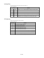
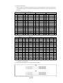
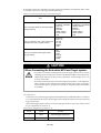
1
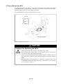
To our customers,
Old Company Name in Catalogs and Other Documents
On April 1st, 2010, NEC Electronics Corporation merged with Renesas Technology
Corporation, and Renesas Electronics Corporation took over all the business of both
companies. Therefore, although the old company name remains in this document, it is a valid
Renesas Electronics document. We appreciate your understanding.
Renesas Electronics website: http://www.renesas.com
April 1st, 2010
Renesas Electronics Corporation
Issued by: Renesas Electronics Corporation (http://www.renesas.com)
Send any inquiries to http://www.renesas.com/inquiry.
Notice
1.
2.
3.
4.
5.
6.
7.
All information included in this document is current as of the date this document is issued. Such information, however, is
subject to change without any prior notice. Before purchasing or using any Renesas Electronics products listed herein, please
confirm the latest product information with a Renesas Electronics sales office. Also, please pay regular and careful attention to
additional and different information to be disclosed by Renesas Electronics such as that disclosed through our website.
Renesas Electronics does not assume any liability for infringement of patents, copyrights, or other intellectual property rights
of third parties by or arising from the use of Renesas Electronics products or technical information described in this document.
No license, express, implied or otherwise, is granted hereby under any patents, copyrights or other intellectual property rights
of Renesas Electronics or others.
You should not alter, modify, copy, or otherwise misappropriate any Renesas Electronics product, whether in whole or in part.
Descriptions of circuits, software and other related information in this document are provided only to illustrate the operation of
semiconductor products and application examples. You are fully responsible for the incorporation of these circuits, software,
and information in the design of your equipment. Renesas Electronics assumes no responsibility for any losses incurred by
you or third parties arising from the use of these circuits, software, or information.
When exporting the products or technology described in this document, you should comply with the applicable export control
laws and regulations and follow the procedures required by such laws and regulations. You should not use Renesas
Electronics products or the technology described in this document for any purpose relating to military applications or use by
the military, including but not limited to the development of weapons of mass destruction. Renesas Electronics products and
technology may not be used for or incorporated into any products or systems whose manufacture, use, or sale is prohibited
under any applicable domestic or foreign laws or regulations.
Renesas Electronics has used reasonable care in preparing the information included in this document, but Renesas Electronics
does not warrant that such information is error free. Renesas Electronics assumes no liability whatsoever for any damages
incurred by you resulting from errors in or omissions from the information included herein.
Renesas Electronics products are classified according to the following three quality grades: “Standard”, “High Quality”, and
“Specific”. The recommended applications for each Renesas Electronics product depends on the product’s quality grade, as
indicated below. You must check the quality grade of each Renesas Electronics product before using it in a particular
application. You may not use any Renesas Electronics product for any application categorized as “Specific” without the prior
written consent of Renesas Electronics. Further, you may not use any Renesas Electronics product for any application for
which it is not intended without the prior written consent of Renesas Electronics. Renesas Electronics shall not be in any way
liable for any damages or losses incurred by you or third parties arising from the use of any Renesas Electronics product for an
application categorized as “Specific” or for which the product is not intended where you have failed to obtain the prior written
consent of Renesas Electronics. The quality grade of each Renesas Electronics product is “Standard” unless otherwise
expressly specified in a Renesas Electronics data sheets or data books, etc.
“Standard”:
8.
9.
10.
11.
12.
Computers; office equipment; communications equipment; test and measurement equipment; audio and visual
equipment; home electronic appliances; machine tools; personal electronic equipment; and industrial robots.
“High Quality”: Transportation equipment (automobiles, trains, ships, etc.); traffic control systems; anti-disaster systems; anticrime systems; safety equipment; and medical equipment not specifically designed for life support.
“Specific”:
Aircraft; aerospace equipment; submersible repeaters; nuclear reactor control systems; medical equipment or
systems for life support (e.g. artificial life support devices or systems), surgical implantations, or healthcare
intervention (e.g. excision, etc.), and any other applications or purposes that pose a direct threat to human life.
You should use the Renesas Electronics products described in this document within the range specified by Renesas Electronics,
especially with respect to the maximum rating, operating supply voltage range, movement power voltage range, heat radiation
characteristics, installation and other product characteristics. Renesas Electronics shall have no liability for malfunctions or
damages arising out of the use of Renesas Electronics products beyond such specified ranges.
Although Renesas Electronics endeavors to improve the quality and reliability of its products, semiconductor products have
specific characteristics such as the occurrence of failure at a certain rate and malfunctions under certain use conditions. Further,
Renesas Electronics products are not subject to radiation resistance design. Please be sure to implement safety measures to
guard them against the possibility of physical injury, and injury or damage caused by fire in the event of the failure of a
Renesas Electronics product, such as safety design for hardware and software including but not limited to redundancy, fire
control and malfunction prevention, appropriate treatment for aging degradation or any other appropriate measures. Because
the evaluation of microcomputer software alone is very difficult, please evaluate the safety of the final products or system
manufactured by you.
Please contact a Renesas Electronics sales office for details as to environmental matters such as the environmental
compatibility of each Renesas Electronics product. Please use Renesas Electronics products in compliance with all applicable
laws and regulations that regulate the inclusion or use of controlled substances, including without limitation, the EU RoHS
Directive. Renesas Electronics assumes no liability for damages or losses occurring as a result of your noncompliance with
applicable laws and regulations.
This document may not be reproduced or duplicated, in any form, in whole or in part, without prior written consent of Renesas
Electronics.
Please contact a Renesas Electronics sales office if you have any questions regarding the information contained in this
document or Renesas Electronics products, or if you have any other inquiries.
(Note 1) “Renesas Electronics” as used in this document means Renesas Electronics Corporation and also includes its majorityowned subsidiaries.
(Note 2) “Renesas Electronics product(s)” means any product developed or manufactured by or for Renesas Electronics.
User’s Manual
M34524T-MCU
User’s Manual
MCU Board for 4524 and 4554 Group MCUs
Rev.2.00 2004.07
* IBM and PC/AT are registered trademarks of International Business Machines Corporation.
* IC61-0644-053 and IC61-0644-088 are products of Yamaichi Electronics Co., Ltd.
Keep safety first in your circuit designs!
• Renesas Technology Corporation and Renesas Solutions Corporation put the maximum effort into making semiconductor products better
and more reliable, but there is always the possibility that trouble may occur with them. Trouble with semiconductors may lead to personal
injury, fire or property damage. Remember to give due consideration to safety when making your circuit designs, with appropriate
measures such as (i) placement of substitutive, auxiliary circuits, (ii) use of nonflammable material or (iii) prevention against any
malfunction or mishap.
Notes regarding these materials
• These materials are intended as a reference to assist our customers in the selection of the Renesas Technology product best suited to
the customer's application; they do not convey any license under any intellectual property rights, or any other rights, belonging to Renesas
Technology Corporation, Renesas Solutions Corporation or a third party.
• Renesas Technology Corporation and Renesas Solutions Corporation assume no responsibility for any damage, or infringement of any
third-party's rights, originating in the use of any product data, diagrams, charts, programs, algorithms, or circuit application examples
contained in these materials.
• All information contained in these materials, including product data, diagrams, charts, programs and algorithms represents information
on products at the time of publication of these materials, and are subject to change by Renesas Technology Corporation and Renesas
Solutions Corporation without notice due to product improvements or other reasons. It is therefore recommended that customers contact
Renesas Technology Corporation, Renesas Solutions Corporation or an authorized Renesas Technology product distributor for the latest
product information before purchasing a product listed herein. The information described here may contain technical inaccuracies or
typographical errors. Renesas Technology Corporation and Renesas Solutions Corporation assume no responsibility for any damage,
liability, or other loss rising from these inaccuracies or errors. Please also pay attention to information published by Renesas Technology
Corporation and Renesas Solutions Corporation by various means, including the Renesas home page (http://www.renesas.com).
• When using any or all of the information contained in these materials, including product data, diagrams, charts, programs, and algorithms,
please be sure to evaluate all information as a total system before making a final decision on the applicability of the information and
products. Renesas Technology Corporation and Renesas Solutions Corporation assume no responsibility for any damage, liability or
other loss resulting from the information contained herein.
• Renesas Technology semiconductors are not designed or manufactured for use in a device or system that is used under circumstances
in which human life is potentially at stake. Please contact Renesas Technology Corporation, Renesas Solutions Corporation or an
authorized Renesas Technology product distributor when considering the use of a product contained herein for any specific purposes,
such as apparatus or systems for transportation, vehicular, medical, aerospace, nuclear, or undersea repeater use.
• The prior written approval of Renesas Technology Corporation and Renesas Solutions Corporation is necessary to reprint or reproduce
in whole or in part these materials.
• If these products or technologies are subject to the Japanese export control restrictions, they must be exported under a license from the
Japanese government and cannot be imported into a country other than the approved destination. Any diversion or reexport contrary to
the export control laws and regulations of Japan and/or the country of destination is prohibited.
• Please contact Renesas Technology Corporation or Renesas Solutions Corporation for further details on these materials or the products
contained therein.
Precautions to be taken when using this product
• This product is a development supporting unit for use in your program development and evaluation stages. In mass-producing your
program you have finished developing, be sure to make a judgment on your own risk that it can be put to practical use by performing
integration test, evaluation, or some experiment else.
• In no event shall Renesas Solutions Corporation be liable for any consequence arising from the use of this product.
• Renesas Solutions Corporation strives to renovate or provide a workaround for product malfunction at some charge or without charge.
However, this does not necessarily mean that Renesas Solutions Corporation guarantees the renovation or the provision under any
circumstances.
• This product has been developed by assuming its use for program development and evaluation in laboratories. Therefore, it does not fall
under the application of Electrical Appliance and Material Safety Law and protection against electromagnetic interference when used in
Japan.
For inquiries about the contents of this document or product, fill in the text file the installer of the emulator debugger generates in the
following directory and email to your local distributor.
\SUPPORT\Product-name\SUPPORT.TXT
Renesas Tools Homepage http://www.renesas.com/en/tools
( 2 / 38 )
Contents
Preface ....................................................................................................................................4
1. Precautions for Safety ......................................................................................................... 5
1.1 Safety Symbols and Meanings ..............................................................................5
2. Contents of the M34524T-MCU ........................................................................................ 9
2.1 Contents of the M34524T-MCU ........................................................................... 9
2.2 Other Necessary Products ................................................................................... 10
3. M34524T-MCU ................................................................................................................ 11
3.1 Outline ................................................................................................................. 11
3.2 Specifications ...................................................................................................... 12
3.3 Switches .............................................................................................................. 13
3.4 Check Pins ........................................................................................................... 14
3.5 Connectors ........................................................................................................... 14
3.6 Connection to the Target System ........................................................................ 18
3.7 How to Replace the MCU ................................................................................... 22
4. Precautions to Be Taken When Debugging a Program .................................................... 23
4.1 Reset Condition ................................................................................................... 23
4.2 Watchdog Timer .................................................................................................. 23
4.3 Operation in RAM Backup Mode ....................................................................... 24
4.4 Port I/O Timings and Characteristics .................................................................. 25
4.5 A-D Converter ..................................................................................................... 26
4.6 System Clock ...................................................................................................... 26
4.7 Real-time Capability of the Timer ...................................................................... 27
4.8 Pullup Transistor Control .................................................................................... 27
4.9 Program Execution (G, GB) ................................................................................ 28
4.10 External Trigger Signal ..................................................................................... 29
4.11 Other Precautions .............................................................................................. 29
5. Connection Circuit Diagrams of the M34524T-MCU ..................................................... 31
6. Pitch Converter Board External Dimensions ................................................................... 33
6.1 PCA4917A and PCA4917B ................................................................................ 33
6.2 PCA4918 ............................................................................................................. 33
7. Maintenance and Guarantee ............................................................................................. 35
7.1 Maintenance ........................................................................................................ 35
7.2 Guarantee ............................................................................................................ 35
7.3 Repair Provisions ................................................................................................ 35
7.4 How to Request for Repair .................................................................................. 36
( 3 / 38 )
Preface
This user's manual describes the specifications of the M34524T-MCU emulator board for the
Renesas 4524 and 4554 Groups of 4-bit CMOS single-chip MCUs. The M34524T-MCU is an MCU
board for the PC4504 emulator. For emulator main unit PC4504 and emulator debugger M3T-PD45,
refer to each user's manual (or online manual).
To use the product properly
Precautions for Safety
• In both this user's manual and on the product itself, several icons are used to insure
proper handling of this product and also to prevent injuries to you or other persons,
or damage to your properties.
• The icons' graphic images and meanings are given in "Chapter 1. Precautions for
Safety". Be sure to read this chapter before using the product.
( 4 / 38 )
1. Precautions for Safety
Both in the M34524T-MCU user's manual and on the product, several icons are used to insure proper
handling of this product and also to prevent injuries to you or other persons, or damage to your
properties.
This chapter describes precautions which should be taken in order to use the M34524T-MCU safely
and properly. Be sure to read this chapter before using this product.
1.1 Safety Symbols and Meanings
WARNING
If the requirements shown in the "WARNING"
sentences are ignored, the equipment may
cause serious personal injury or death.
CAUTION
If the requirements shown in the "CAUTION"
sentences are ignored, the equipment may
malfunction.
IMPORTANT
It means important information on using this
product.
In addition to the three above, the following are also used as appropriate.
means WARNING or CAUTION.
Example:
CAUTION AGAINST AN ELECTRIC SHOCK
means PROHIBITION.
Example:
DISASSEMBLY PROHIBITED
means A FORCIBLE ACTION.
Example:
UNPLUG THE POWER CABLE FROM THE RECEPTACLE.
The following pages describe the symbols "WARNING", "CAUTION", and "IMPORTANT".
( 5 / 38 )
WARNING
Warning for Installation:
• Do not set this product in water or areas of high humidity. Spilling water or some other liquid into
the main unit can cause an unrepairable damage.
Warning for Use Environment:
• This equipment is to be used in an environment with a maximum ambient temperature of 35°C. Care
should be taken that this temperature is not exceeded.
CAUTION
Cautions to Be Taken for This Product:
• Do not disassemble or modify this product. Disassembling or modifying this product can cause
damage. Disassembling and modifying the product will void your warranty.
• Use caution when handling the main unit. Be careful not to apply a mechanical shock.
• Do not pull the emulator probe (64-wire half-pitch cable etc.) to disconnect from the emulator main
unit.
• Do not use inch-size screws for this equipment. The screws used in this equipment are all ISO
(meter-size) type screws. When replacing screws, use same type screws as equipped before.
( 6 / 38 )
IMPORTANT
Notes on Differences between Actual MCUs and the Emulator:
• Emulator operation differs from emulation of a mask MCU, as listed below. For details refer to
"Chapter 4. Precautions to Be Taken When Debugging a Program" (page 23).
(1) Reset condition
(2) Operation of the watchdog timer function
(3) Operation in RAM backup mode
(4) Port I/O timings and characteristics
(5) A-D conversion function
• Therefore, always be sure to evaluate your system with an evaluation MCU (OTP version). Also,
be sure to perform board-mounted evaluation with CS (Commercial Sample) version MCU to
make final confirmation of device operation before starting mask production.
Note on the Target System:
• Make sure that the target's supply voltage is + 3.0 V or + 5.0 V. Therefore the target's supply voltage
should be in the range of + 3.0 V ±10% or + 5.0 V ±10%.
Notes on Connecting the Target System:
• When connecting the target system, be sure to shut off the power of the emulator and the target
system.
• Connect the emulator probe carefully.
• When connecting the emulator probe, use care not to twist the cable. An excessive twist may cause
breaking of the wire.
( 7 / 38 )
IMPORTANT
Note on MCU board Installation:
• Before installing and removing the MCU board, always be sure to power off the PC4504 emulator
main unit and unplug its power cord from the outlet.
Note on Registers that Can be Operated from the M3T-PD45
• The table below lists the registers that can be operated from the M3T-PD45. The "Yes" in the table
means that the register can be operated; the "No" means that the register can not be operated.
Register
Reference Modification
Remarks
Register
Reference Modification
Remarks
PC
Yes
Yes
W5
Yes
Yes
CY
Yes
Yes
W6
Yes
Yes
A
Yes
Yes
J1
Yes
Yes
4524 only
B
Yes
Yes
Q1
Yes
Yes
4524 only
D
Yes
Yes
Q2
Yes
Yes
4524 only
E
Yes
Yes
Q3
Yes
Yes
4524 only
No
Yes
Yes
K0
Yes
Yes
Y
Yes
Yes
K1
Yes
Yes
Z
Yes
Yes
K2
Yes
Yes
V1
Yes
Yes
PU0
Yes
Yes
V2
Yes
Yes
PU1
Yes
Yes
I1
Yes
Yes
FR0
No
Yes
I2
Yes
Yes
I3
Yes
Yes
MR
Yes
Yes
FR3
No
Yes
PA
No
Yes
L1
Yes
Yes
W1
Yes
Yes
L2
No
Yes
W2
Yes
Yes
L3
No
Yes
4524 only
W3
Yes
Yes
SI
Yes
Yes
4524 only
W4
Yes
Yes
-
-
-
-
4524 only
( 8 / 38 )
FR1
No
Yes
FR2
No
Yes
4524 only
2. Contents of the M34524T-MCU
2.1 Contents of the M34524T-MCU
Table 2.1 shows the contents of the M34524T-MCU package. When unpacking your M34524TMCU package, check to see that all of these components are included.
Table 2.1 Contents of the M34524T-MCU
Item
Product name
Quantity
1
M34524T-MCU
1
2
M34554EDFP (for replacement)
1
3
64-wire half-pitch cables (50 cm)
2
4
2-wire cable for external trigger signal (50 cm)
1
5
Pitch converter board PCA4917A
1
6
Pitch converter board PCA4917B
1
7
Pitch converter board PCA4918
1
8
Oscillator circuit board OSC-2 (connector J1 mounted)
1
9
M34524T-MCU User's Manual (this manual)
1
10
M34524T-MCU User's Manual (Japanese)
1
IMPORTANT
Notes on Components of this Product:
• If you find any item missing or faulty, or any suggestion, contact your local
distributor.
• Keep the packaging carton and cushion material of the M34524T-MCU to transport
it for repair or for other purposes in the future.
• M34524T-MCU has an oscillator circuit board OSC-2 for 6.0 MHz (main clock) and
32.768 kHz (sub clock) that is incorporated when shipped from the factory. In
addition, it comes with an oscillator circuit board OSC-2, with only connector J1
mounted.
( 9 / 38 )
2.2 Other Necessary Products
To bring forward your program development with the 4524 and 4554 Groups of 4-bit MCUs, the
products listed in Table 2.2 are necessary in addition to those contained in the package listed in Table
2.1. Get them separately when necessary.
Table 2.2 Other necessary products required for developing the 4524 and 4554 Group MCUs
Item
Product name
1
Emulator debugger M3T-PD45
2
Emulator main unit PC4504
3
IC socket IC61-0644-088*1 (required when using the PCA4918)
4
Programming adapter PCA7448
*1 For details on this product, contact:
Yamaichi Electronics Co., Ltd.
http://www.yamaichi.co.jp/e/index.shtml
( 10 / 38 )
3. M34524T-MCU
3.1 Outline
By using with the PC4504 emulator main unit, the M34524T-MCU can make up an emulator system
which can be operated by a host machine. Figure 3.1 shows the emulator system configuration. For
the connection to the target system, see "3.6 Connection to the Target System" (page 18).
Figure 3.1 Emulator system configuration
Figure 3.2 shows the positions of the switches and connectors.
Figure 3.2 Positions of the switches and connectors
( 11 / 38 )
3.2 Specifications
Table 3.1 lists the specifications of the M34524T-MCU.
Table 3.1 M34524T-MCU specifications
Applicable MCUs
4524 Group
4554 Group*1
Evaluation MCU
Mounted clock
4524 Group
M34524EDFP (preinstalled)
4554 Group
M34554EDFP (included)
Main clock: 6.0 MHz (OSC-2 [6.0 MHz mounted] used)
Sub clock: 32.768 kHz (OSC-2 [32.768 kHz mounted] used)
Maximum operating
clock frequency
Divide-by-8 mode (f(XIN)/8)
Divide-by-4 mode (f(XIN)/4)
5V
6.0 MHz
Divide-by-2 mode (f(XIN)/2)
Through mode (f(XIN))
Divide-by-8 mode (f(XIN)/8)
6.0 MHz
Divide-by-4 mode (f(XIN)/4)
3V
Target system voltage
Power supply
Port emulation
Divide-by-2 mode (f(XIN)/2)
4.4 MHz
Through mode (f(XIN))
3 V ±10% or 5 V ±10%
Supplied by the PC4504's internal power supply (+5 V, +12 V).
3 V is generated from +12 V.
Port
Output type
Direction
Device used
P00--P03
P10--P13
D0--D5
N-ch open drain
or
CMOS*2
D7, D8, D9
N-ch open drain
Emulated functions
Key-on wakeup input
in RAM backup mode
Pullup resistor control
Port output type control
Input
Input/output
Input/output
Pin
Output
74ALS641 (N-ch)
74VHC125 (CMOS)
Input/Output: 74HC4066
Factor of return
P00--P03
L-level detection
P10--P13
L-level detection
INT0, INT1
Edge detection
or
level detection*3
Pin
Control resister
P00--P03
PU0
P10--P13
PU1
Pin
Control resister
P00--P03
P10--P13
D0--D5
Board dimensions
74HC245
FR0
FR1, FR2
233.35 x 135.00 x 1.60 mm
Operating temperature 5 to 35°C (non-condensing)
Product configuration - M34524T-MCU
- M34554EDFP
- 64-wire half-pitch cables (2 pieces)
- PCA4918
- PCA4917A
- PCA4917B
- 2-wire cable for external trigger signal
- OSC-2 (parts not mounted)
*1 Available by changing MCUs
*2 N-ch open drain output and CMOS output are selectable by the control resister.
*3 It is possible to select the leading edge, trailing edge, both edges, L-level or H-level as a factor
of return by the control resister.
( 12 / 38 )
3.3 Switches
Tables 3.2 lists the functions of the switches and their factory-settings.
Table 3.2 Functions of switches
Description
Switch position
Label
OFF
ON
OFF
Does not output the VDD of the M34524TMCU to the target system.
ON
ON
OFF
Outputs the VDD of the M34524T-MCU
to the target system.
Factory-setting
SW1
SW2
Set the MCU's ROM size.
• Set "8" (M8)
• Set "C" (MC)
• Set "D" (ED)
ROMSIZE
OFF
D
5V
Operates the evaluation MCU on the
M34524T-MCU at +5 V.
5V
3V
SW3
5V
Operates the evaluation MCU on the
M34524T-MCU at + 3 V.
3V
5V
3V
524
554
524
Operates for the 4524 Group.
554
554
524
Operates for the 4554 Group.
SW4
524
*1 To debug the 4554 Group MCUs, it is necessary to replace the evaluation MCU to the included
M34554EDFP. For how to replace the MCU, refer to "3.7 How to Replace the MCU" (page 22).
CAUTION
Caution for Setting the Switches:
• Before changing switch settings, be sure to shut off the power.
( 13 / 38 )
3.4 Check Pins
The M34524T-MCU has the check pins listed in Table 3.3.
Table 3.3 Check pins
Pin
Function
TP1
VDD
Outputs +3 V or +5 V (MCU voltage) according to the setting of SW3.
TP2
XIN
Outputs an instruction clock of the MCU.
TP3
GND
Ground
TP4
RUN*/STOP Held low when executing a user program, held high when it is stopped.
TP5
WRST
Held high when executing WRST instruction, and it is possible to check the
initialization cycle of a watchdog timer by observing pulse widths.
3.5 Connectors
Table 3.4 lists the functions of the connectors.
Table 3.4 Connectors
Connector
Function
J1
Connects the evaluation MCU bus.
J2
Connects the monitor CPU bus.
J3
Connects the target system. (64-pin)
J4
Connects the target system. (64-pin)
J5
Connects the oscillator circuit board OSC-2 (main clock). (4-pin)
J6
Connects the oscillator circuit board OSC-2 (sub clock). (4-pin)
J7
For an external trigger signal. (2-pin)
( 14 / 38 )
(1) Connectors J3 and J4
Tables 3.5 and 3.6 list the pin assignments of the 64-wire half-pitch connectors J3 and J4 for
connecting the PCA4917A, PCA4917B and PCA4918. And Figure 3.3 shows the connector J3
pin layout.
Table 3.5 Pin assignments of connector J3
Line A
Line B
Line C
Line D
Pin No.
Signal
I/O
Pin No.
Signal
I/O
Pin No.
Signal
Pin No.
Signal
1
SEG16
O
1
SEG15
O
1
GND
I/O
1
GND
2
SEG17
O
2
SEG14
O
2
GND
2
GND
3
SEG18
O
3
SEG13
O
3
GND
3
GND
4
SEG19
O
4
SEG12
O
4
GND
4
GND
5
P43(SEG20)
I/O
5
SEG11
O
5
GND
5
GND
6
P42(SEG21)
I/O
6
SEG10
O
6
GND
6
GND
7
P41(SEG22)
I/O
7
SEG9
O
7
GND
7
GND
8
P40(SEG23)
I/O
8
SEG8
O
8
GND
8
GND
9
P33/AIN7(SEG24)
I/O
9
SEG7
O
9
GND
9
GND
10
P32/AIN6(SEG25)
I/O
10
SEG6
O
10
GND
10
GND
11
P31/AIN7(SEG26)
I/O
11
SEG5
O
11
GND
11
GND
12
P30/AIN4(SEG27)
I/O
12
SEG4
O
12
GND
12
GND
13
P23/AIN3(SEG28)
I/O
13
SEG3
O
13
GND
13
GND
14
P22/AIN2(SEG29)
I/O
14
VLC1/SEG2
I/O
14
GND
14
GND
15
P21/AIN1(SEG30)
I/O
15
VLC2/SEG1
I/O
15
GND
15
GND
16
P20/AIN0(SEG31)
I/O
16
VLC3/SEG0
I/O
16
GND
16
GND
I/O
Table 3.6 Pin assignments of connector J4
Line A
Line B
Line C
Line D
Pin No.
Signal
I/O
Pin No.
Signal
I/O
Pin No.
Signal
1
D9/INT1
I/O
1
COM0
O
1
2
D8/INT0
I/O
2
COM1
O
3
C/CNTR1
I/O
3
COM2
O
4
D7/CNTR0
I/O
4
COM3
O
5
RESET
I
5
P00
I/O
5
GND
5
GND
6
XIN
-
6
P01
I/O
6
GND
6
GND
7
XOUT
-
8
VSS
9
VDD
10
XCOUT
-
I/O
Pin No.
Signal
GND
1
GND
2
GND
2
GND
3
GND
3
GND
4
GND
4
GND
7
P02
I/O
7
GND
7
GND
8
P03
I/O
8
GND
8
GND
9
P10
I/O
9
GND
9
GND
10
P11
I/O
10
GND
10
GND
11
XCIN
-
11
P12
I/O
11
GND
11
GND
12
VDCE
-
12
P13
I/O
12
GND
12
GND
13
CNVSS
-
13
D0
I/O
13
GND
13
GND
14
D6/SCK
I/O
14
D1
I/O
14
GND
14
GND
15
D5/SOUT
I/O
15
D2
I/O
15
GND
15
GND
16
D4/SIN
I/O
16
D3
I/O
16
GND
16
GND
I/O
*1 "I" in the direction column denotes "Input"; "O" denotes "Output"; "I/O" denotes "Input/output";
"-" denotes "No connection".
*2 The signals in parentheses are for the 4554 Group MCUs.
Figure 3.3 Connectors J3 and J4 pin layout
( 15 / 38 )
Some signals which are connected to the target system are emulated by the M34524T-MCU. Table
3.7 lists the connections of the target system and each pin.
Table 3.7 Connection of the target system and each pin
Signal
Item
4524 Group
4554 Group
Pins connected directly to the target system
(8 types 39 pins)
• P20/AIN0--P23/AIN3
• P30/AIN4--P33/AIN7
• P40--P43
• D6/SCK
• C/CNTR1
• SEG0--SEG19
• COM0--COM3
• VSS
• P20/SEG31--P23/SEG28
• P30/SEG27--P33/SEG24
• SEG20--SEG23
• D6/SCK
• C/CNTR1
• SEG0--SEG19
• COM0--COM3
• VSS
Pins connected to the target system via
emulation circuit etc. (6 types 19 pins)
• P00--P03
• P10--P13
• D0--D5
• D7--D9
• RESET
• VDD
Pins not connected to the target system
(6 types 6 pins)
• XIN
• XOUT
• XCIN
• XCOUT
• CNVSS
• VDCE
CAUTION
When Connecting the Evaluation MCU and Target system:
• Pin VDD is not used for inputting power from the target system, but it is used for
outputting power from the power circuit on the M34524T-MCU to the target system.
Output of pin VDD (ON or OFF) is set by switch SW1, and the voltage (3 V or 5 V)
is set by switch SW3.
• Pins XIN and XCIN are input from the oscillator board OSC-2 on the M34524TMCU, and they are not input from the oscillator on the target system. To change a
system clock frequency, prepare parts required for using the oscillator board OSC2 (included).
(2) Connector J7
Connect the 2-wire external trigger signal cable included with your M34524T-MCU to connector
J7. Connect the black clip of the external trigger cable to GND, and use the white clip for external
trigger signal input.
The external trigger signal is used for event input of trigger breaks or trace points. Table 3.8 lists
the pin assignments of connector J7.
Table 3.8 Pin assignments of connector J7
Pin No.
Signal
Function
1
TRIG
External trigger signal input
2
GND
GND
( 16 / 38 )
(3) Connectors J5 and J6
Connectors J5 and J6 are connectors used to connect an oscillator circuit board OSC-2. Table 3.9
lists the pin assignments of connectors J5 and J6. Figure 3.4 shows the pin layout of connectors
J5 and J6.
For the 6.0MHz and 32.768kHz operation with the oscillator circuit board OSC-2, see Figure 3.5.
Table 3.9 Pin assignments of connectors J5 and J6
Pin No.
Signal
Function
1
VCC
Power supply
2
GND
GND
3
CLK
Clock input
4
GND
GND
J5 (J6)
Figure 3.4 Pin layout of connectors J5 and J6
Figure 3.5 Connection diagrams of the oscillator circuits
CAUTION
When Changing a Clock Frequency:
• When changing a clock frequency, be sure to shut off the power supply to replace
the oscillator circuit board (OSC-2).
• For details about the oscillation circuit constant, consult your oscillator manufacturer.
( 17 / 38 )
3.6 Connection to the Target System
There are two types for connecting the M34524T-MCU and the target system as shown below.
(1) When using the pitch converter boards PCA4917A and PCA4917B
Connect the PCA4917A and PCA4917B included with this product to the 2.54-mm-pitch 32-pin
dual-in-line pin on the target system.
Figure 3.6 depicts the M34524T-MCU board connected to the target system using the PCA4917A
and PCA4917B. Table 3.10 lists the connector signal assignments of the PCA4917A and
PCA4917B. Figure 3.7 shows the pin layout of the PCA4917A and PCA4917B.
Figure 3.6 Connection to the target system using the PCA4917A and PCA4917B
CAUTION
Note on Connecting the Cable:
• Always shut OFF power before connecting the target system. Otherwise internal
circuits of the target system and the emulator may be damaged.
( 18 / 38 )
Table 3.10 Pin assignments of the PCA4917A and PCA4917B
PCA4917A J2
PCA4917B J2
1
SEG16
64
SEG15
17
D9/INT1
48
COM0
2
SEG17
63
SEG14
18
D8/INT0
47
COM1
3
SEG18
62
SEG13
19
C/CNTR1
46
COM2
4
SEG19
61
SEG12
20
D7/CNTR0
45
COM3
5
P43(SEG20)
60
SEG11
21
RESET
44
P00
6
P42(SEG21)
59
SEG10
22
XIN
43
P01
7
P41(SEG22)
58
SEG9
23
XOUT
42
P02
8
P40(SEG23)
57
SEG8
24
VSS
41
P03
9
P33/AIN7(SEG24)
56
SEG7
25
VDD
40
P10
10
P32/AIN6(SEG25)
55
SEG6
26
XCOUT
39
P11
11
P31/AIN5(SEG26)
54
SEG5
27
XCIN
38
P12
12
P30/AIN4(SEG27)
53
SEG4
28
VDCE
37
P13
13
P23/AIN3(SEG28)
52
SEG3
29
CNVSS
36
D0
14
P22/AIN2(SEG29)
51
VLC1/SEG2
30
D6/SCK
35
D1
15
P21/AIN1(SEG30)
50
VLC2/SEG1
31
D5/SOUT
34
D2
16
P20/AIN0(SEG31)
49
VLC3/SEG0
32
D4/SIN
33
D3
* The signals in parentheses are for the 4554 Group.
Figure 3.7 Pin layouts of the PCA4917A and PCA4917B
CAUTION
When Connecting the M34524T-MCU and Target system:
• Pin VDD is not used for inputting power from the target system, but it is used for
outputting power from the power circuit on the M34524T-MCU to the target system.
However, when supplying the target system with an external power, do not set
switch SW1 to "ON", because the target system does not need power from the
M34524T-MCU. For details on the switch settings, see "3.3 Switches" (page 13).
• Pin XIN is input from the oscillator board OSC-2 on the M34524T-MCU, and it is
not input from the oscillator on the target system. To change a system clock
frequency, change the frequency of the oscillator board OSC-2.
( 19 / 38 )
(2) When using the pitch converter board PCA4918
Connect the PCA4918 included with this product to the 64-pin LCC socket (IC61-0644-088 etc.
made by Yamaichi Electronics Co., Ltd.) on the target system.
Figure 3.8 depicts the M34524T-MCU board connected to the target system using the PCA4918.
Table 3.11 lists the connector signal assignments of the PCA4918. Figure 3.9 shows the pin layout
of the PCA4918.
Figure 3.8 Connecting to the target system
CAUTION
Note on Connecting the Cable:
• Always shut OFF power before connecting the target system. Otherwise, internal
circuits of the target system and the emulator may be damaged.
• For details on the IC61-0644-088, contact Yamaichi Electronics Co., Ltd.
http://www.yamaichi.co.jp/e/index.shtml
( 20 / 38 )
Table 3.11 Pin assignments of the PCA4918
PCA4918
1
SEG16
17
D9/INT1
33
D3
49
VLC3/SEG0
2
SEG17
18
D8/INT0
34
D2
50
VLC2/SEG1
3
SEG18
19
C/CNTR1
35
D1
51
VLC1/SEG2
4
SEG19
20
D7/CNTR0
36
D0
52
SEG3
5
P43(SEG20)
21
RESET
37
P13
53
SEG4
6
P42(SEG21)
22
XIN
38
P12
54
SEG5
7
P41(SEG22)
23
XOUT
39
P11
55
SEG6
8
P40(SEG23)
24
VSS
40
P10
56
SEG7
9
P33/AIN7(SEG24)
25
VDD
41
P03
57
SEG8
10
P32/AIN6(SEG25)
26
XCOUT
42
P02
58
SEG9
11
P31/AIN5(SEG26)
27
XCIN
43
P01
59
SEG10
12
P30/AIN4(SEG27)
28
VDCE
44
P00
60
SEG11
13
P23/AIN3(SEG28)
29
CNVSS
45
COM3
61
SEG12
14
P22/AIN2(SEG29)
30
D6/SCK
46
COM2
62
SEG13
15
P21/AIN1(SEG30)
31
D5/SOUT
47
COM1
63
SEG14
16
P20/AIN0(SEG31)
32
D4/SIN
48
COM0
64
SEG15
* The signals in parentheses are for the 4554 Group.
Figure 3.9 Pin layout of the PCA4918
CAUTION
When Connecting the M34524T-MCU and Target system:
• The VDD is not used for inputting power from the target system, but it is used for
outputting power from the power circuit on the M34524T-MCU to the target system.
However, when supplying the target system with an external power, do not set
switch SW1 to "ON", because the target system does not need power from the
M34524T-MCU. For details on the switch settings, see "3.3 Switches" (page 13).
• The XIN is input from the oscillator board OSC-2 on the M34524T-MCU, and it is
not input from the oscillator on the target system. To change a system clock
frequency, change the frequency of the oscillator board OSC-2.
( 21 / 38 )
3.7 How to Replace the MCU
For debugging the 4554 Group MCUs, it is necessary to replace the evaluation MCU to the included
M34554EDFP. When replacing the MCU, match the No. 1 pin of the IC socket and that of the MCU.
Incorrect insertion may cause a fatal damage to the MCU.
The M34524EDFP is mounted when shipped from the factory.
Figure 3.10 Replacing the MCU
CAUTION
Cautions for Replacing the MCU:
• Before replacing the MCU, be sure to shut off the power supply.
• When mounting the evaluation MCU, be sure to match the No. 1 pin. Incorrect
insertion may cause a fatal damage to the MCU.
• When opening and closing the IC socket, hold the adapter horizontally. Otherwise
the inside of the IC socket may become damaged and cause an electrical insulation
failure.
• When debugging a 4554 Group MCU, it is necessary to replace the MCU to the
included M34554EDFP and change the setting of switch SW4. For switch setting,
see "3.3 Switches" (page 13).
( 22 / 38 )
4. Precautions to Be Taken When Debugging a Program
4.1 Reset Condition
The M34524T-MCU uses a 74HC14 for its RESET signal input buffer, so that its electrical
characteristics differ from those of an actual MCU. Table 4.1 lists the RESET signal input
characteristics of the M34524T-MCU.
Table 4.1 RESET signal input characteristics
Item
H-level threshold voltage
L-level threshold voltage
Hysteresis voltage
Symbol
VP
VN
VH
Voltage
Min.
Max.
VCC = 2.0 V
1.0 V
1.5 V
VCC = 4.5 V
2.3 V
3.15 V
VCC = 6.0 V
3.0 V
4.2 V
VCC = 2.0 V
0.3 V
0.9 V
VCC = 4.5 V
1.13 V
2.0 V
VCC = 6.0 V
1.5 V
2.6 V
VCC = 2.0 V
0.3 V
1.0 V
VCC = 4.5 V
0.6 V
1.4 V
VCC = 6.0 V
0.8 V
1.7 V
4.2 Watchdog Timer
The M34524T-MCU does not have an operational watchdog timer. Therefore, use an evaluation
MCU (OTP version) to verify the operation associated with a watchdog timer.
The M34524T-MCU outputs a signal whose waveform is shown below from check pin TP5 during
WRST instruction execution cycles. This signal allows you to check the initialization cycle of a
watchdog timer.
System clock
XIN
CNVSS
WRST
Figure 4.1 Waveform output from check pin TP5
( 23 / 38 )
4.3 Operation in RAM Backup Mode
In RAM backup mode, the M34524T-MCU operates differently from the actual MCUs. Although the
actual MCU enters RAM backup mode depending on a combination of the EPOF and POF or POF2
instructions, the M34524T-MCU is placed in RAM backup mode by only executing the POF or POF2
instruction. The EPOF instruction has no effect on the M34524T-MCU.
[Actual MCU]
Program example 4.1
Switched to RAM backup mode
RC
INY
EPOF
POF
•
•
[M34524T-MCU]
Switched to RAM backup mode
[Actual MCU]
Program example 4.2
RC
INY
POF
•
•
Not switched to RAM backup mode
[M34524T-MCU]
Switched to RAM backup mode
( 24 / 38 )
4.4 Port I/O Timings and Characteristics
(1) Port input timings
Port input timings are the same as with actual MCUs.
(2) Port output timings
When using the M34524T-MCU, output timings are different from those of the actual MCUs,
because the following ports that are configured with the port emulation circuits:
• Ports D0--D5
• Ports P00--P03
• Ports P10--P13
With actual MCUs, changes occur at the beginning of the T3 state of an output instruction. With
the M34524T-MCU, changes occur at the beginning of the T2 state of the next output instruction.
Figure 4.2 shows the port output timings of the actual MCUs and M34524T-MCU. For the other
ports, the output timings are the same as with the actual MCUs.
Output instruction
System clock
XIN
Ports D, P0, P1
output timings
on actual MCUs
Ports D, P0, P1
output timings of
M34524T-MCU
Figure 4.2 Ports D, P0 and P1 output timings
( 25 / 38 )
Next output instruction
(3) Port I/O Characteristics
With the M34524T-MCU, port I/O characteristics are different from actual MCUs because there
are emulation circuits in ports P00--P03, P10--P13 and D0--D5. Table 4.2 lists port I/O
characteristics of the M34524T-MCU.
Table 4.2 Emulation port I/O characteristics
Port
Device
Item
VIH
Input
74HC245
VIL
P0, P1,
D0--D5
IOH
74ALS641
VOL
Output*1
VIH
74VHC125
VIL
Input/
Output
D7, D8,
D9
RON
74HC4066
Condition
Min.
Standard
Max.
VCC = 2.0 V
1.50 V
-
-
VCC = 4.5 V
3.15 V
-
-
VCC = 2.0 V
-
-
0.50 V
VCC = 4.5 V
-
-
1.35 V
-
-
0.1 mA
VCC = 4.5 V
-
0.35 V
0.5 V
VCC = 2.0 V
1.50 V
-
-
VCC = 4.5 V
3.15 V
-
-
VCC = 2.0 V
-
-
0.50 V
VCC = 4.5 V
-
-
1.35 V
VCC = 2.0 V
-
160 Ω
-
-
96 Ω
170 Ω
-
70 Ω
100 Ω
-
10 Ω
-
VCC = 4.5 V
RON VCC = 4.5 V
Remarks
*1 According to the setting of the output method control register FRx, change its device for output
in the emulation circuit.
• When N-ch open drain output chosen: 74ALS641
• When CMOS output chosen: 74VHC125
4.5 A-D Converter
For the M34524T-MCU, its voltage is fixed at 3 V or 5 V. Therefore, because of the difference of
voltage, the results of its A/D conversions are slightly different from the theoretical values. And, some
characteristics are different from those of actual MCUs, because a flat cable and pitch converter board
and other devices are used between the evaluation MCU and target system.
4.6 System Clock
Depending on the supply voltage and operation mode, use one of the following frequencies listed in
Table 4.3 for the system clock.
Table 4.3 M34524T-MCU operating frequencies
Voltage
Mode
Frequency
Divide-by-8
Divide-by-4
6.0 MHz or less
5V
Divide-by-2
Through
Divide-by-8
Divide-by-4
6.0 MHz or less
3V
Divide-by-2
Through
4.4 MHz or less
* To change a clock frequency, attach the necessary parts to the oscillator circuit board OSC-2 that
are included with the M34524T-MCU package.
For details about the oscillation circuit constant, consult your oscillator manufacturer.
( 26 / 38 )
4.7 Real-time Capability of the Timer
The PC4504 and M34524T-MCU have their internal clock operating even during emulation, so that
the timer values keep changing.
Examples:
(1) When single-stepping the program
(2) When registers or internal RAM are referenced or modified
4.8 Pullup Transistor Control
Because the M34524T-MCU has an emulation circuit present in ports P0 and P1, it cannot use the
MCU's internal pullup transistors. Therefore, the M34524T-MCU controls on/off of external pullup
resistors by decoding the pullup control register transfer instructions (TPU0A and TPU1A).
The M34524T-MCU contains 150kΩ pullup resistors for use with the 4524 and 4554 Groups. If these
pullup resistors need to be changed, replace the RA5 resister array.
( 27 / 38 )
4.9 Program Execution (G, GB)
The PC4504 and M34524T-MCU's hardware is subject to the following restrictions with respect to
the operation of the program execution commands (G and GB).
(1) Continuous description of instructions
Hardware breakpoints set in a continuous description of instructions following one after another
do not cause a break to occur in the continuous description of instructions. A break occurs only
after fetching the address where the continuous description of instructions is discontinued. (See
Program example 4.3)
However, a break does occur even in a continuous description of instructions when an external
trigger break or forced break is encountered. For execution to be resumed in this case, you need
to make sure that the execution start address is next to the continuous description of instructions.
(See Program example 4.4)
Program example 4.3
POINT:
POINT+2:
LA
LA
LA
XAM
0
1
2
3
; Continuous description of instructions
If a break is set at POINT, execution is halted immediately before the XAM instruction at address
POINT+2.
Program example 4.4
POINT:
POINT+1:
POINT+2:
LA
LA
LA
XAM
0
1
2
3
; Continuous description of instructions
If a forced or external trigger break is applied at POINT, execution is halted at POINT +1. When
resuming program execution after the break, make sure that the start address is at POINT+2,
an address immediately after the continuous description of instructions is discontinued.
(2) Skip instructions (e.g. SNZP, INY, DEY, SZB, SEAM, SZC and RTS)
In cases when a skip instruction skips the next instruction, a breakpoint set in the skipped
instruction does not cause execution to halt. (See Program examples 4.5 and 4.6)
Program example 4.5
POINT:
POINT A:
LXY
SDZ
B
TAM
0, 0
jmp_adr
0
•
•
; Skips when D(0) = 0
If a breakpoint is set at address POINT, the program stops before executing the instruction at
POINT when D(0) = 0, but does not stop running when D(0) = 1 because the instruction at POINT
is skipped. To stop the program immediately after executing a skip instruction, be sure to set
a breakpoint at both POINT and POINT_A.
Program example 4.6
POINT:
RC
INY
TABP
LA
0
•
•
; Skips when (Y) = 0
If a break with pass count is set at address POINT, the count is taken and execution is halted
only when the instruction at address POINT is executed.
( 28 / 38 )
4.10 External Trigger Signal
(1) External trigger signal input timing
The latch timing of the external trigger signal is shown in Figure 4.3.
Instruction
Next Instruction
System clock
XIN
External trigger
signal TRIG
Figure 4.3 Latch timing of the external trigger signal
(2) External trigger signal input characteristics
Trigger breaks work according to the conditions (leading edge/trailing edge) of signals input from
the external trigger cable. The external trigger signals of the trace points and the external trigger
signals of the break points use the same signals. The input characteristics of the external trigger
signals are shown in Table 4.4 below. See the table before using external trigger signals.
Table 4.4 External trigger signal input characteristics
Item
Symbol
H-level voltage
VIH
L-level voltage
VIL
Voltage
Min.
Max.
VCC = 2.0 V
1.5 V
-
VCC = 4.5 V
3.15 V
-
VCC = 2.0 V
-
0.5 V
VCC = 4.5 V
-
1.35 V
4.11 Other Precautions
The M34524T-MCU cannot evaluate systems that use some functions as described below. In such
a case, therefore, the system needs to be evaluated using an evaluation-purpose MCU (OTP version).
(1) Because an emulation circuit exists in the RESET pin, systems that use RESET output cannot be
evaluated.
(2) Because the M34524T-MCU has its power supply voltage fixed at 3 V or 5 V, systems that use
a power-down detect function cannot be evaluated.
(3) Power-on reset operation cannot be verified.
(4) Because the M34524T-MCU is clocked by the system clock on the board, its clock source cannot
be changed to an on-chip oscillator or CR oscillator. When using an emulator, do not use the
CMCK and CRCK instructions in the program.
(5) Because an emulation circuit exists in the D4/SIN and D5/SOUT pins, serial I/O cannot be
emulated in external clock synchronized mode. Serial I/O can only be emulated in internal clock
synchronized mode.
(6) When the main clock is stopped in low-speed mode, the M34524T-MCU cannot operate
normally. When using the emulator, always set bit 1 of the clock control register (main clock
oscillator circuit control bit: MR1) to "0" (main clock enabled).
( 29 / 38 )
MEMO
( 30 / 38 )
5. Connection Circuit Diagrams of the M34524T-MCU
Figures 5.1 and 5.2 show the connection circuit diagrams of the M34524T-MCU. These circuit
diagrams depict the M34524T-MCU connection centering on circuits connected to the target system.
Emulator control blocks and other similar circuits that are not connected to the target system are
omitted in this diagram.
∗ denotes control signal
Figure 5.1 Connection circuit diagram (1/2)
( 31 / 38 )
∗ denotes control signal
Figure 5.2 Connection circuit diagram (2/2)
( 32 / 38 )
6. Pitch Converter Board External Dimensions
6.1 PCA4917A and PCA4917B
Figure 6.1 shows external dimensions of the PCA4917A and PCA4917B.
Unit: mm
Figure 6.1 External dimensions of the PCA4917A and PCA4917B
6.2 PCA4918
Figure 6.2 shows external dimensions of the PCA4918.
Unit: mm
Figure 6.2 External dimensions of the PCA4918
( 33 / 38 )
MEMO
( 34 / 38 )
7. Maintenance and Guarantee
7.1 Maintenance
If dust or dirt collects on any equipment of your emulation system, wipe it off with a dry soft cloth.
Do not use thinner or other solvents because these chemicals can cause the equipment's surface
coating to separate.
7.2 Guarantee
If your product becomes faulty within one year after its purchase while being used under good
conditions by observing "Precautions for Safety" described in Chapter 1 of this user's manual, we will
repair or replace your faulty product free of charge. Note, however, that if your product's fault is raised
by any one of the following causes, we will repair it or replace it with new one with extra-charge:
• Misuse, abuse, or use under extraordinary conditions
• Unauthorized repair, remodeling, maintenance, and so on
• Inadequate user's system or misuse of it
• Fires, earthquakes, and other unexpected disasters
In the above cases, contact your local distributor. If your product is being leased, consult the leasing
company or the owner.
7.3 Repair Provisions
(1) Repair with extra-charge
The products elapsed more than one year after purchase can be repaired with extra-charge.
(2) Replacement with extra-charge
If your product's fault falls in any of the following categories, the fault will be corrected by
replacing the entire product instead of repair, or you will be advised to purchase new one,
depending on the severity of the fault.
• Faulty or broken mechanical portions
• Flaw, separation, or rust in coated or plated portions
• Flaw or cracks in plastic portions
• Faults or breakage caused by improper use or unauthorized repair or modification
• Heavily damaged electric circuits due to overvoltage, overcurrent or shorting of power supply
• Cracks in the printed circuit board or burnt-down patterns
• Wide range of faults that makes replacement less expensive than repair
• Unlocatable or unidentified faults
(3) Expiration of the repair period
When a period of one year elapses after the model was dropped from production, repairing
products of the model may become impossible.
(4) Transportation fees at sending your product for repair
Please send your product to us for repair at your expense.
( 35 / 38 )
7.4 How to Request for Repair
If your product is found faulty, follow the procedure below to send your product for repair.
Customer
Fill in the Repair Request Sheet included with this product, then send it
along with this product for repair to your local distributor. Make sure
that information in the Repair Request Sheet is written in as much detail
as possible to facilitate repair.
Distributor
After checking the contents of fault, the distributor should please send
the faulty product along with the Repair Request Sheet to Renesas
Solutions Corp.
Renesas Solutions
When the faulty product is repaired, it will be returned to the customer
at the earliest convenience.
CAUTION
Note on Transporting the Product:
• When sending your product for repair, use the packing box and cushion material supplied with this
product when delivered to you and specify handling caution for it to be handled as precision
equipment. If packing of your product is not complete, it may be damaged during transportation.
When you pack your product in a bag, make sure to use conductive polyvinyl supplied with this
product (usually a blue bag). When you use other bags, they may cause a trouble on your product
because of static electricity.
( 36 / 38 )
M34524T-MCU User's Manual
Rev.2.00
July 1, 2004
REJ10J0275-0200Z
COPYRIGHT ©2003-2004 RENESAS TECHNOLOGY CORPORATION
AND RENESAS SOLUTIONS CORPORATION ALL RIGHTS RESERVED
M34524T-MCU
User’s Manual
1753, Shimonumabe, Nakahara-ku, Kawasaki-shi, Kanagawa 211-8668 Japan
REJ10J0275-0200Z