1
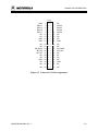
MMCEVB1200UM/D REV 1 DECEMBER 1998 MMCEVB1200PV EVALUATION BOARD USER’S MANUAL © MOTOROLA Inc., 1998; All Rights Reserved Motorola reserves the right to make changes without further notice to any products herein to improve reliability, function, or design. Motorola does not assume any liability arising out of the application or use of any product or circuit described herein; neither does it convey any license under its patent rights nor the rights of others. Motorola products are not designed, intended, or authorized for use as components in systems intended for surgical implant into the body, or other application in which the failure of the Motorola product could create a situation where personal injury or death may occur. Should Buyer purchase or use Motorola products for any such unintended or unauthorized application, Buyer shall indemnify and hold Motorola and its officers, employees, subsidiaries, affiliates, and distributors harmless against all claims, costs, damages, and expenses, and reasonable attorney fees arising out of, directly or indirectly, any claim of personal injury or death associated with such unintended or unauthorized use, even if such claim alleges that Motorola was negligent regarding the design or manufacture of the part. Motorola and the Motorola logo are registered trademarks of Motorola Inc. M•CORE and OnCE are trademarks of Motorola, Inc. Other trademarks belong to their respective owners. Motorola Inc. is an Equal Opportunity/Affirmative Action Employer. Caution: ESD Protection M•CORE development systems include open-construction printed circuit boards that contain static-sensitive components. These boards are subject to damage from electrostatic discharge (ESD). To prevent such damage, you must use static-safe work surfaces and grounding straps, as defined in ANSI/EOS/ESD S6.1 and ANSI/EOS/ESD S4.1. All handling of these boards must be in accordance with ANSI/EAI 625. CONTENTS CONTENTS CHAPTER 1 INTRODUCTION 1.1 1.2 1.3 EVB Features .....................................................................................................................1-1 System and User Requirements...........................................................................................1-2 EVB Layout.........................................................................................................................1-2 CHAPTER 2 CONFIGURATION 2.1 Setting Jumper Headers ......................................................................................................2-1 2.1.1 Setting the SRAM Bank 1 Header (W2) ....................................................................2-5 2.1.2 Selecting the FLASH Byte/Word Select Headers (W3, W6).....................................2-6 2.1.3 Setting the SRAM Bank 0 Header (W8) ....................................................................2-7 2.1.4 Setting the Startup Vector Select Header (W9)..........................................................2-8 2.1.5 Setting the FLASH Chip Select Header (W12)..........................................................2-9 2.1.6 Setting the Serial Port Enable Header (W14)...........................................................2-10 2.2 Making Computer-System Connections ...........................................................................2-11 2.3 Performing the EVB Self-Test .........................................................................................2-12 2.4 Memory Maps ...................................................................................................................2-13 CHAPTER 3 OPERATION 3.1 Debugging Embedded Code ...............................................................................................3-1 3.1.1 Using the Picobug Debug Monitor.............................................................................3-1 3.1.2 Picobug Sample Session.............................................................................................3-3 3.1.3 Using the GNU Source-Level Debugger....................................................................3-6 3.2 Downloading to FLASH Memory.......................................................................................3-7 3.2.1 Using the FLASH Programmer ..................................................................................3-7 3.2.2 Restoring Factory Programming ..............................................................................3-10 3.3 Controlling EVB LEDs .....................................................................................................3-13 MMCEVB1200UM/D Rev 1 iii CONTENTS CHAPTER 4 CONNECTOR INFORMATION 4.1 4.2 I/O and Interrupt Connectors (P1, P2A, P2B) ....................................................................4-1 OnCE Connector (P5) .........................................................................................................4-7 INDEX .................................................................................................................................. index-1 FIGURES 1-1 3-1 3-2 3-3 4-1 4-2 4-3 4-4 MMCEVB1200PV Evaluation Board ................................................................................1-2 FLASH Programmer Main Screen ......................................................................................3-7 Picobug Protocol Selection ................................................................................................3-8 Memory Contents Display ................................................................................................3-11 Connector P1 Pin Assignments ...........................................................................................4-1 Connector P2A Pin Assignments .......................................................................................4-3 Connector P2B Pin Assignments .......................................................................................4-5 OnCE Connector P5 Pin Assignments ...............................................................................4-7 TABLES 1-1 2-1 2-2 2-3 3-1 3-2 4-1 4-2 4-3 4-4 iv MMCEVB1200PV Evaluation Board Specifications .........................................................1-3 Jumper Header Positions.....................................................................................................2-2 W14 Jumper Signals .........................................................................................................2-10 MMC2001 Address-Decoded Memory Map.....................................................................2-13 Picobug Commands.............................................................................................................3-2 LED Registers and Addresses ...........................................................................................3-13 Connector P1 Signal Descriptions.......................................................................................4-2 Connector P2A Signal Descriptions....................................................................................4-4 Connector P2B Signal Descriptions ....................................................................................4-6 OnCE Connector P5 Signal Descriptions............................................................................4-8 Rev 1 MMCEVB1200UM/D INTRODUCTION CHAPTER 1 INTRODUCTION This user’s manual explains connection, configuration, and operation information for the MMCEVB1200PV Evaluation Board (EVB), a standalone development tool of Motorola’s M•CORE family. The EVB lets you use the Picobug debug monitor, through an RS232 connection to your computer. In conjunction with the Picobug monitor, you may use the GNU source-level debugger. The EVB also has a OnCE connector, enabling you to use a debugging application that requires one. Motorola’s FLASH programmer lets you download your code into the EVB’s SRAM (for execution) or FLASH memory (for storage in non-volatile memory). Should your application overwrite factory programming in the FLASH memory device, you can use the FLASH programmer to restore the factory programming. 1.1 EVB FEATURES The EVB features: • 512K-by-16 FLASH memory, at 90 nanoseconds • Two 64K-by-16 SRAM memories, at 70 nanoseconds • 3.3-volt power regulator • Two RS232 channels for serial communication. These channels use internal universal asynchronous receiver/transmitters (UARTs). • 14-pin JTAG/OnCE debug connector • Three 40-pin I/O and interrupt connectors • Address decoding: direct chip select from the processor. • Jumper headers for such configuration items as FLASH byte/word use. • Motorola’s FLASH programmer • Picobug debug monitor and GNU source-level debugger (from the Free Software Foundation) • Ability to use debugging software from one or more other manufacturers. (An example is SingleStep debugging software, from Software Development Systems.) MMCEVB1200UM/D Rev 1 1-1 INTRODUCTION 1.2 SYSTEM AND USER REQUIREMENTS Your EVB requires 5-volt (± 0.25 volt) input power, at 250 milliamperes. You need an IBM PC or compatible computer, running the Windows 95 or WindowsNT (version 4.0) operating system. The computer requires a Pentium (or equivalent) microprocessor, 16 megabytes of RAM, 50 megabytes of free harddisk space, an SVGA color monitor, and an RS232 serial-communications port. You also need a C compiler, an M•CORE assembler, and an M•CORE linker. To use the Picobug debug monitor, you also need Hyperterminal or a comparable terminal-emulation program. To get the most from your EVB, you must be an experienced C or M•CORE assembly programmer. 1.3 EVB LAYOUT Figure 1-1 shows the layout of the EVB. Jumper header W2 selects the SRAM bank 1 chip select. Jumper headers W3 and W6 configure byte or word mode for FLASH memory. Jumper header W8 selects the SRAM bank 0 chip select. Jumper header W9 selects the startup vector. Jumper header W12 selects the FLASH chip select. Jumper header W14 enables or disables the serial ports, and also configures the EVB for its self-test. W2 U1 U2 U3 W3 W6 S1 P5 W8 DS1 DS4 U7 P1 W9 W12 J8 P2A J9 J10 P2B F1 W14 DS5 Figure 1-1. MMCEVB1200PV Evaluation Board 1-2 Rev 1 MMCEVB1200UM/D INTRODUCTION Connectors P1, P2A, and P2B are the I/O and interrupt connectors. Connector P5 is the OnCE connector. Connector J8 is the power connector. Connectors J9 and J10 are the RS232 serial communication connectors. Switch S1 is the reset switch. Location F1 is for the EVB fuse. Yellow LEDs DS1 through DS4 light to confirm that the EVB passed its self-test. Green LED DS5 lights to confirm that the EVB is receiving +5-volt input power. The MMC2001 resident MCU is at location U7. SRAM memory devices are at locations U1 and U3. The FLASH memory device is at location U2. Some unpopulated EVB locations are available for users who want to add optional extra functionality. For example, specific users may want to install a backup battery connector at location P6 (between connector P5 and jumper header W9). Other specific users may want to install low-frequency and high-frequency external coaxial oscillator input connectors at locations J5 and J6, respectively. (These locations are below and to the right of jumper header W9.) Table 1-1 lists EVB specifications. Table 1-1. MMCEVB1200PV Evaluation Board Specifications Characteristic Specifications MCU extension I/O ports HCMOS compatible Operating temperature 0° to 40° C Storage temperature -40° to +85° C Relative humidity 0 to 90% (non-condensing) Clock 32 MHz Power requirements 5 volts dc, from a separate power source Dimensions 5.75 x 6.0 inches (146 x 152 mm) Weight 4.5 ounces (128 g) MMCEVB1200UM/D Rev 1 1-3 INTRODUCTION 1-4 Rev 1 MMCEVB1200UM/D CONFIGURATION CHAPTER 2 CONFIGURATION This chapter explains how to configure your EVB, and how to hook it up to your computer system. 2.1 SETTING JUMPER HEADERS Your EVB has seven jumper headers, numbered from W2 through W14. Table 21 is a summary of settings for these headers; paragraphs 2.1.1 through 2.1.6 give additional information. NOTE The EVB does not use jumper header numbers W1, W4, W5, W7, W10, W11, or W13. MMCEVB1200UM/D Rev 1 2-1 CONFIGURATION Table 2-1. Jumper Header Positions Header SRAM Bank 1 Select, W2 (Only 1 jumper in this header; do not use position A.) Position Effect Selects chip select 0 to control SRAM bank 1. W2 SRAM 1 1 GB1# 2 A CS0# B CS1# C CS2# D 8 7 Selects chip select 1 to control SRAM bank 1. W2 SRAM 1 1 GB1# 2 A CS0# B CS1# C CS2# Factory setting. D 8 7 Selects chip select 2 to control SRAM bank 1. W2 SRAM 1 1 GB1# 2 A CS0# B CS1# C CS2# D 8 7 FLASH Byte/Word Select, W3, W6 1 Configures word mode for FLASH memory. 1 Factory setting. 1 Configures byte mode for FLASH memory. B A W3 3 WORD/BYTE W6 BYTE B A W3 3 WORD/BYTE 1 W6 BYTE 2-2 Rev 1 MMCEVB1200UM/D CONFIGURATION Table 2-1. Jumper Header Positions (continued) Header SRAM Bank 0 Chip Select, W8 (Only 1 jumper in this header; do not use position A.) Position W8 SRAM 0 1 A 2 GB0# B CS0# C CS1# D CS2# 8 7 W8 SRAM 0 1 A 2 GB0# B CS0# C CS1# D CS2# 8 7 W8 SRAM 0 1 A 2 GB0# B CS0# C CS1# D CS2# 8 7 Startup Vector Select, W9 Effect Selects chip select 0 to control SRAM bank 0. Selects chip select 1 to control SRAM bank 0. Selects chip select 2 to control SRAM bank 0. Factory setting. Upon power-up, selects the startup vector from the lowest address of the external chip-select 0 device. (Usually this is FLASH memory.) Correct configuration for EVB self-test. 1 W9 MOD Factory setting Upon power-up, selects the startup vector from the lowest address of MCU internal ROM. Invokes the Mbug debugger. 1 W9 MOD Also the correct setting for the FLASH programmer. FLASH Chip Select, W12 (Only 1 jumper in this header; do not use position A.) MMCEVB1200UM/D Rev 1 W12 FLASH 1 A 2 GFCS# B CS0# C CS1# D CS2# 8 7 Selects chip select 0 to control FLASH memory. Factory setting. 2-3 CONFIGURATION Table 2-1. Jumper Header Positions (continued) Header Position FLASH Chip Select, W12 (continued) Effect Selects chip select 1 to control FLASH memory. W12 FLASH 1 A (Only 1 jumper in this header; do not use position A.) 2 GFCS# B CS0# C CS1# D CS2# 8 7 Selects chip select 2 to control FLASH memory. W12 FLASH 1 A B CS0# C CS1# D CS2# 8 7 Serial Port Enable, W14 A 2 GFCS# W14 SP ENA B C D E F G 2 14 1 A W14 SP ENA B C D E F 14 13 A W14 SP ENA B C D E F Disconnects all serial-port signals. G 2 14 1 13 A 2-4 Connects port 0 serial-port signals, disconnects port 1 serial port signals. G 1 1 Factory setting. 13 2 2 Connectss all serial-port (UART) signals to RS232 transcievers. W14 SP ENA B C D E F Configures the EVB self-test. G 14 13 Rev 1 MMCEVB1200UM/D CONFIGURATION 2.1.1 Setting the SRAM Bank 1 Header (W2) Jumper header W2 selects one of three chip selects for SRAM bank 1. The diagram below shows the factory configuration: the fabricated jumper at position C selects chip select 1. W2 SRAM 1 1 GB1# 2 A CS0# B CS1# C CS2# D 8 7 Fabricated jumper Alternatively, you may select chip selects 0 or 2. For either of these selections, reposition the W2 fabricated jumper to position B or D, respectively. NOTE You must use jumper headers W2, W8, and W12 to configure chip selects 0, 1, and 2. Although any of these jumper headers can configure any chip select, there must not be any duplication; all three chip selects must be configured. CAUTION There must be one and only one jumper in header W2 (in position B, C, or D). Having a jumper in position A, having multiple jumpers, or having no jumpers could damage the EVB. MMCEVB1200UM/D Rev 1 2-5 CONFIGURATION 2.1.2 Setting the FLASH Byte/Word Select Headers (W3, W6) Jumper headers W3 and W6 determine whether the EVB uses FLASH in word or byte mode. The diagram below shows the factory configuration: the fabricated jumper at W3 position B and no fabricated jumper in header W6 configures word mode. Fabricated jumper B A 1 W3 3 WORD/BYTE 1 W6 BYTE To configure byte mode for the FLASH: • Reposition the W3 jumper to position A, and • Put a jumper in header W6. NOTE Do not put the W3 jumper in position A unless you also put a jumper in header W6. Do not put a jumper in header W6 if you put the W3 jumper in position B. 2-6 Rev 1 MMCEVB1200UM/D CONFIGURATION 2.1.3 Setting the SRAM Bank 0 Header (W8) Jumper header W8 selects one of three chip selects for SRAM bank 0. The diagram below shows the factory configuration: the fabricated jumper at position D selects chip select 2. W8 SRAM 0 Fabricated jumper 1 A 2 GB0# B CS0# C CS1# D CS2# 8 7 Alternatively, you may select chip selects 0 or 1. For either of these selections, reposition the W8 fabricated jumper to position B or C, respectively. NOTE You must use jumper headers W2, W8, and W12 to configure chip selects 0, 1, and 2. Although any of these jumper headers can configure any chip select, there must not be any duplication; all three chip selects must be configured. CAUTION There must be one and only one jumper in header W8 (in position B, C, or D). Having a jumper in position A, having multiple jumpers, or having no jumpers could damage the EVB. MMCEVB1200UM/D Rev 1 2-7 CONFIGURATION 2.1.4 Setting the Startup Vector Select Header (W9) Jumper header W9 selects the startup vector that the MCU uses upon power-up. The diagram below shows the factory configuration: the fabricated jumper installed in this header selects the vector in the external chip-select 0 device (usually the FLASH memory). 1 W9 MOD Alternatively, you can select the vector in MCU internal ROM. To do so, remove the jumper from header W9. 2-8 Rev 1 MMCEVB1200UM/D CONFIGURATION 2.1.5 Setting the FLASH Chip Select Header (W12) Jumper header W12 selects one of three chip selects for FLASH memory. The diagram below shows the factory configuration: the fabricated jumper at position B selects chip select 0. (This is the only correct configuration if you will boot up with the Picobug monitor.) W12 FLASH Fabricated jumper 1 A 2 GFCS# B CS0# C CS1# D CS2# 8 7 Alternatively, you may select chip selects 1 or 2. For either of these selections, reposition the W12 fabricated jumper to position C or D, respectively. NOTE You must use jumper headers W2, W8, and W12 to configure chip selects 0, 1, and 2. Although any of these jumper headers can configure any chip select, there must not be any duplication; all three chip selects must be configured. CAUTION There must be one and only one jumper in header W12 (in position B, C, or D). Having a jumper in position A, having multiple jumpers, or having no jumpers could damage the EVB. MMCEVB1200UM/D Rev 1 2-9 CONFIGURATION 2.1.6 Setting the Serial Port Enable Header (W14) Jumper header W14 connects or disconnects serial-port (UART) signals from RS232 transceivers. The diagram below shows the factory configuration: the seven fabricated jumpers, in positions A through G, connect the UART signals. A W14 SP ENA B C D E F 2 G 14 1 13 Fabricated jumpers Table 2-2 lists the serial-port signals that correspond to each W14 jumper position. To disconnect a signal, making it available for other use, remove the corresponding jumper. (Table 2-1 shows such a possible configuration: jumpers removed from positions C and F, disconnecting the port 0 signals.) Table 2-2. W14 Jumper Signals UART Signal Jumper Position TXD0 (Transmit data, port 0) A CTS0 (Clear to send, port 0) B TXD1 (Transmit data, port 1) C RXD0 (Receive data, port 0) D RTS0 (Ready to send, port 0) E RXD1 (Receive data, port 1) F (1) Transceiver Standby G (1) Removing the jumper from position G puts driver and receiver outputs in a high-impedance state. To make sure that UART signals of other positons are connected to RS232 transceivers, make sure that a jumper is in position G. 2-10 Rev 1 MMCEVB1200UM/D CONFIGURATION NOTE To configure an EVB self-test, remove the jumpers from W14 positions C and D, then insert one of the jumpers turned 90 degrees, so that the jumper connects W14 pins 5 and 7. At the end of the self-test, restore W14 to its correct configuration for operation. 2.2 MAKING COMPUTER-SYSTEM CONNECTIONS When you have configured your EVB, you are ready to connect it to your computer system: 1. If you will use the Picobug-GNU debug monitor software, the Motorola FLASH programmer, or another application that needs RS232 connection to port 0, connect an RS232 cable between EVB connector J10 and the appropriate serial port of your computer. If your application will use port 1, connect the port 1 RS232 cable between EVB connector J9 and the appropriate serial port of your computer. 2. If your application will use the OnCE connector, connect a OnCEcompatible cable between EVB connector P5 and the appropriate connector of your computer. (Chapter 4 gives pin assignments and signal descriptions for connector P5.) 3. Make sure that your +5-volt power supply is turned off (or disconnected from line power). Connect the power supply’s ground wire to pin 1 (black) of EVB connector J8. Connect the power supply’s power wire to pin 2 (red) of connector J8. 4. If you have not already done so, apply power to your computer. Turn on your +5-volt power supply (or connect it to line power): the green LED (DS5) lights to confirm that the EVB is powered. (Should the DS5 LED not light, you may need to replace the fuse at location F1, next to power connector J8. Use a BUS GMA-1.5A fuse, or compatible.) 5. This completes system connections; you are ready to perform an EVB selftest, per the instructions of paragraph 2.3, below. You are ready to begin debugging or other development activities, per the instructions of Chapter 3. 6. (Optional) For scope observation of specific I/O or interrupt signals, you may use connectors P1, P2A, or P2B. You may clip individual lines to the pins of these connectors, or use appropriate connectors. (Chapter 4 gives pin assignments and signal descriptions for these connectors.) MMCEVB1200UM/D Rev 1 2-11 CONFIGURATION 2.3 PERFORMING THE EVB SELF-TEST Once you have configured your EVB, you can perform a self-test of EVB components. 1. If your EVB is powered, turn off or disconnect power. The green LED (DS5) goes out. 2. Make sure that a fabricated jumper is in jumper header W9. 3. Remove the fabricated jumpers from positions C and D of jumper header W14. Turn one of these jumpers 90 degrees, then reinsert it, so that it connects W14 pins 5 and 7. 4. Apply power to the EVB. The green LED (DS5) comes on to confirm power. The EVB automatically begins its self-test. 5. The four yellow LEDs (DS1 through DS4) flicker during the self-test (approximately one minute), then light without flickering to confirm that the EVB passed the self-test. 6. If, at the end of the self-test, any of the yellow LEDs does not light without flickering, the EVB fails the self-test. The computer displays a failure message that will help you find and correct the problem. After you do so, repeat the self-test. (Should the failure persist, you may need to contact Motorola customer support for assistance.) 7. When the EVB passes the self-test, disconnect power, restore jumper header W14 to its operating configuration, then restore power. This completes the self-test. 2-12 Rev 1 MMCEVB1200UM/D CONFIGURATION 2.4 MEMORY MAPS The configuration of jumper headers W2, W8, and W12 determines which chip selects are active. Table 2-3 lists the memory-map starting and ending addresses for all such possibilities (bold type indicates the factory configuration). Table 2-3. MMC2001 Address-Decoded Memory Map Memory Jumper Header, Jumper Position Chip Select Starting Address Ending Address FLASH W12 B CS0 0x2D00_0000 0x2D0F_FFFF W12 C CS1 0x2F00_0000 0x2F0F_FFFF W12 D CS2 0x2E00_0000 0x2E0F_FFFF W8 B CS0 0x2D00_0000 0x2D0F_FFFF W8 C CS1 0x2F00_0000 0x2F0F_FFFF W8 D CS2 0x2E00_0000 0x2E0F_FFFF W2 B CS0 0x2D00_0000 0x2D0F_FFFF W2 C CS1 0x2F00_0000 0x2F0F_FFFF W2 D CS2 0x2E00_0000 0x2E0F_FFFF SRAM Bank 0 SRAM Bank 1 As the table shows, the factory configuration: • Puts FLASH memory into the chip-select 0 memory space (addresses 0x2D00_0000 through 0x2D0F_FFFF), and • Puts SRAM bank 0 memory into the chip-select 2 memory space (addresses 0x2E00_0000 through 0x2E0F_FFFF). • Puts SRAM bank 1 memory into the chip-select 1 memory space (addresses 0x2F00_0000 through 0x2F0F_FFFF). NOTE Each SRAM bank occupies 64 kilobytes of memory: one eighth of the megabyte a chip select reserves. Accordingly, the EVB mirrors SRAM contents. That is, it puts eight copies of the data into the megabyte of memory. This makes memory contents contiguous, despite the smaller size of an SRAM bank. MMCEVB1200UM/D Rev 1 2-13 CONFIGURATION 2-14 Rev 1 MMCEVB1200UM/D OPERATION CHAPTER 3 OPERATION This chapter explains how to begin using debugging tools available for your MMCEVB1200PV Evaluation Board, as well as how to use Motorola’s FLASH programmer. 3.1 DEBUGGING EMBEDDED CODE With your EVB, you may use the Picobug debug monitor, as standalone software. Optionally, you may use the GNU source-level debugger with the Picobug monitor. Other firms may produce still additional software to run, test, and modify the code you develop for embedding in an MMC2001 MCU. 3.1.1 Using the Picobug Debug Monitor The Picobug debug monitor comes burned into the FLASH memory device of your EVB (location U3). Before you start the Picobug monitor, make sure that you have an RS232 connection between EVB connector J10 and a serial port of your computer. To start the Picobug monitor, for use as a standalone debugger: 1. Make sure that power is not applied to your EVB. 2. Activate Hyperterminal or a comparable terminal-emulation program. (If you use a different terminal-emulation program, you must make corresponding changes in the commands and menu selections of these instructions, and in the instructions of paragraph 3.1.2.) 3. From the File menu, select Properties. This opens a properties dialog box. 4. Click on the Configure button of the dialog box. This opens a configuration dialog box. 5. Use the configuration dialog box to set the operating speed (19,200) and the correct communications port (for example, COM1). Click the OK button of the dialog box. 6. The Picobug monitor starts automatically, as soon as you apply power to the EVB. Note the command prompt:picobug>. MMCEVB1200UM/D Rev 1 3-1 OPERATION To use the Picobug debug monitor, merely enter commands at the prompt. Table 3-1 explains these commands. To see a list of these commands on your computer screen, enter a question mark or the extra command help at the command prompt. Table 3-1. Picobug Commands Command Explanation br [address] Breakpoint: • With optional address value, sets a new breakpoint at that address. • Without any address value, lists all current breakpoints. g [address] Go: • With optional address value, starts code execution from that address. • Without any address value, starts code execution from the current program-counter value. In either case, execution stops when it arrives at a breakpoint. gr Go to Return: Executes code from the current program-counter value to the return address of the calling routine. (Should execution arrive at a breakpoint before encountering the return address, execution stops at the breakpoint.) gt address Go to Address: Executes code from the current program-counter value to the specified address value. (Should execution arrive at a breakpoint before encountering the specified address, execution stops at the breakpoint.) lo [address] Download: • With optional address value, downloads a binary image to that address in SRAM. • Without any address value, downloads to SRAM an S-record text file. md address1 address2 [;size] Memory Display: Displays memory contents from the address1 value to the address2 value. The optional size value specifies the format: b (bytes, the default), h (half words), w (words), or i (instructions). mds address [;size] Memory Display: Displays 256 bytes of memory contents, beginning at the address value. The optional size value specifies the format: b (bytes, the default), h (half words), w (words), or i (instructions). 3-2 Rev 1 MMCEVB1200UM/D OPERATION Table 3-1. Picobug Commands (continued) Command Explanation mm address [value] [;size] Modify Memory: • With optional value parameter value, assigns that value to the address location. • Without any value parameter value, prompts for a value for the address location, then prompts for a new value for the next location. To stop modification, enter a period instead of a new value. • The optional size value, specifies the format: b (bytes, the default), h (half words), w (words), or i (instructions). nobr [address] No Breakpoint: • With optional address value, removes the breakpoint from that address. • Without any address value, removes all the breakpoints. reset Reset: Resets the CPU and peripherals. rd [name] Register Display: • With optional name value, displays the value of that CPU register. • Without any name value, displays the values of all CPU registers. rm name value Register Modify: Assigns the value parameter value to the name CPU register. t Trace (Step): Single steps one instruction; identical to the s command. s Step (Trace): Single steps one instruction; identical to the t command. 3.1.2 Picobug Sample Session 1. This sample session begins with the Picobug prompt: picobug> 2. To see the contents of all registers, enter the Register Display (rd) command without any name value: picobug> rd The system responds with a display such as this: pc psr ss0-ss4 r0-r7 r8-r15 30000286 epc 30000286 fpc 80000100 epsr 80000100 fpsr bad0beef 20000c00 20008000 20010042 300027f8 00000050 0000ea60 30005f94 0010a000 00020000 20000c00 300067c0 MMCEVB1200UM/D Rev 1 0010a000 00020000 00000801 vbr 30005c00 30006708 80070101 00000200 00000040 00000000 30005f94 10005000 30000286 3-3 OPERATION 3. To see the contents of a specific register, such as the epc register, enter the Register Display (rd) command with the name value: picobug> rd epc The system responds with a display such as this: epc: 30000286 4. To see the contents of a specific memory location, enter the Memory Display (md) command with the location address. An optional size value (in this case w, for word) may be part of the command: picobug> md 0x30001000 ;w The system responds with a display such as this: 30001000: 8EF0B37E 5. To see the contents of a memory range, enter the Memory Display (md) command with the beginning and ending addresses. An optional size value (in this case b, for byte) may be part of the command: picobug> md 0x30000000 0x30000010 ;b The system responds with a display such as this: 30000000: . 30000010: 8E F0 00 55 55 55 55 0E 22 9E E8 03 20 0D 20 0E $..UUUU."… . F7 6. To download into SRAM a program executable, in S-record format, enter the Download (lo) command without any address value: picobug> lo The system waits for you to send the program executable file. To do so, open the Transfer menu and select Send Text File. This opens a file-select dialog box. Use this dialog box to specify the appropriate S-record file, then click on the Open button. When the file-select dialog box disappears, press the Enter key of your keyboard. (Pressing the keyboard Enter key adds a necessary line-feed character to the end of the S-record file.) As soon as the download is complete (this may take several minutes), the Picobug prompt reappears: picobug> 3-4 Rev 1 MMCEVB1200UM/D OPERATION 7. To see the new contents of registers, enter the Register Display (rd) command again, without any name value: picobug> rd The system responds with an updated display, which shows that the pc register value reflects the start of the program just downloaded: pc psr ss0-ss4 r0-r7 r8-r15 3000022a epc 2d00108a fpc 80000000 epsr 80070101 fpsr bad0beef 20000c00 20008000 20010042 bad0beef 00000050 00000000 d89f69ab 0010a000 300066b8 300067d7 30006948 0010a000 00020000 00000801 vbr 30005c00 30005f20 80000000 00000200 00000024 30006714 30006708 300067c8 2d0001c4 8. To set a breakpoint at address 0x3000025C, enter this address as part of the Breakpoint (br) command: picobug> br 0x3000025c The Picobug prompt reappears, confirming that the system set the breakpoint: picobug> 9. To see the list of breakpoints, enter the Breakpoint (br) command without any address value: picobug> br The system responds with the addresses of breakpoints, in this case only the breakpoint set in step 8: 3000025C 10. To start program execution, enter the Go (g) command: picobug> g In this instance, the breakpoint set during step 8 stops code execution. The system responds with this new display of register values: At breakpoint!! pc 3000025c epc 3000025c fpc psr 80000100 epsr 80000100 fpsr ss0-ss4 bad0beef 20000c00 20008000 20010042 r0-r7 300027f8 00000050 0000ea60 d89f69ab r8-r15 0010a000 300066b8 300067d7 30006948 MMCEVB1200UM/D Rev 1 0010a000 00020000 00000801 vbr 30005c00 30005f20 80000000 00000200 00000040 30006714 30006708 10005010 300002a2 3-5 OPERATION 11. To remove all breakpoints, enter the No Breakpoint (nobr) command, without any address value: picobug> nobr The Picobug prompt reappears, confirming that the system has removed the breakpoints: picobug> 12. To see the list of breakpoints again, once more enter the Breakpoint (br) command without any address value: picobug> br As there are no longer any breakpoints, the system responds with the Picobug prompt: picobug> 13. To continue with this example session, enter another appropriate command. For example, to resume program execution, enter the Go (g) command. 14. To end your Picobug session, remove power from the EVB and close the terminal-emulation program. 3.1.3 Using the GNU Source-Level Debugger The GNU source-level debugger is on the CD-ROM that comes with your EVB. This GNU software works with the Picobug debug monitor to provide sourcelevel debugging for your code. The EVB product release guide gives the instructions for loading the GNU software, and for making any connections different from standalone Picobug connections. 3-6 Rev 1 MMCEVB1200UM/D OPERATION 3.2 DOWNLOADING TO FLASH MEMORY Motorola’s FLASH programmer lets you program your code into FLASH memory, verify that FLASH contents match those of a download file, display the contents of FLASH memory, erase FLASH memory, or erase a sector of FLASH memory. 3.2.1 Using the FLASH Programmer Follow these steps to use the programmer: 1. If you have not already installed the FLASH programmer onto your computer hard disk, do so. The EVB product release guide includes installation instructions. 2. Reset the EVB, by pressing switch S1. 3. Start the FLASH programmer. The main screen (Figure 3-1) appears. Figure 3-1. FLASH Programmer Main Screen NOTE Figure 3-1 shows field values appropriate for using the FLASH programmer with an EVB. Except as explained in the instructions below, selecting different values for these fields could cause errors. MMCEVB1200UM/D Rev 1 3-7 OPERATION 4. Go to the File field, at the upper left of the main screen. • If you know the full pathname of the file to be programmed, enter the pathname in this field. • If you do not know the full pathname of the file to be programmed, click on the Browse button. This brings up a standard file-select dialog box: select the file and click on the OK button. This returns you to the main screen, entering the pathname in the File field. 5. Use the Flash area of the main screen to configure the FLASH type, bus width, and size. In the Base Address field, enter the FLASH starting address for the chip select you configured via jumper header W12: • For chip select 0, enter base address 0x2d000000. • For chip select 1, enter base address 0x2f000000. • For chip select 2, enter base address 0x2e000000. 6. In the Communications area of the main screen, use the Port field to specify the PC serial port, and use the Speed field to specify the communications rate (19200 bps). Use the Protocol field to specify the communications protocol: • If your computer connects to the EVB through a serial port, and the EVB system software is intact, specify RS232 (Picobug monitor). Figure 3-2 illustrates this selection. Figure 3-2. Picobug Protocol Selection 3-8 • If your computer connects to the EVB OnCE connector through an EBDI box, specify ESL • If your computer connects to the EVB through a serial port, but the EVB system software has been deleted, specify RS232 (Mbug monitor). Rev 1 MMCEVB1200UM/D OPERATION NOTES If you select the RS232 (Mbug monitor) protocol, a prompt tells you to remove the W9 jumper and reset the EVB. Even if you just have reset the EVB, you must reset it again, after removing the W9 jumper. You may set the protocol, port, and speed only once during each programmer session. To make another change in any Communications-area setting, you must exit, then restart, the FLASH programmer. 7. Go to the CMB field, near the lower center of the main screen. Make sure that the field specifies EVB1200. Make sure that the Download Algorithm box is checked. This completes the programmer setup. You are ready for the programming actions that correspond to the buttons along the right edge of the main screen. 8. To program FLASH memory, click on the Program button. The software downloads the file you specified, displaying a progress message. A Download successful message appears at the end of downloading: you are ready to use the code in FLASH memory. • If this is the first programming action of this FLASH programmer session, the software downloads an algorithm file before downloading the file you specified. A progress message appears during the downloading of this algorithm file. • If the software cannot find the algorithm file, an appropriate error message identifies the file. Click on the message’s OK button to bring up a file-select dialog box, then use this dialog box to specify the location of the algorithm file. If necessary, recopy the file from the transmittal CD-ROM. Click on the OK button to resume programming FLASH memory. • The error message Flash is not blank indicates that you must erase the Flash. To do so, click on the message’s OK button. Erasure takes 20 to 30 seconds, then FLASH programming resumes. • The error message Unable to Validate Flash configuration indicates some problem with the programming. A likely such problem is that the chip select base address does not correspond to the configured chip select. Correct the problem, then click again on the Program button. MMCEVB1200UM/D Rev 1 3-9 OPERATION NOTE Another possible cause of validation failure is that the link control file of user code specifies SRAM, not FLASH, as the download destination. You must correct such a problem in the user code. 9. To verify that the contents of Flash memory match the selected download file, click on the Verify button. A progress message appears as verification begins. A Verify successful message appears at the end of verification. • If this is the first programming action of this FLASH programmer session, the software downloads an algorithm file before verifying FLASH. A progress message appears during the downloading of this algorithm file. (Should the software be unable to find the algorithm file, an appropriate error message appears, as explained under the program FLASH memory step, above.) • If verification fails, an error message specifies the location that did not have the expected contents. • To recover from a verification failure, try programming Flash again, to replace the selected download file. NOTE Another possible cause of verification failure is that the link control file of user code specifies SRAM, not FLASH, as the download destination. You must correct such a problem in the user code. 10. To erase FLASH memory, click on the Erase Flash button. The programmer erases all contents of the FLASH memory except for sector 0 (which contains the system software). Erasing takes 20 to 30 seconds. If this is the first programming action of this FLASH programmer session, the software downloads an algorithm file before erasing FLASH. A progress message appears during the downloading of this algorithm file. (Should the software be unable to find the algorithm file, an appropriate error message appears, as explained under the program FLASH memory step, above.) 11. To erase a sector of FLASH memory, click on the Erase Sector button. This brings up the Flash Sector Number dialog box. Enter the number of the sector to be erased, then click on the OK button. 3-10 Rev 1 MMCEVB1200UM/D OPERATION If this is the first programming action of this FLASH programmer session, the software downloads an algorithm file before erasing the FLASH sector. A progress message appears during the downloading of this algorithm file. (Should the software be unable to find the algorithm file, an appropriate error message appears, as explained under the program FLASH memory step, above.) NOTE The target FLASH device has 16 sectors, 0 through 15, each of 64 kilobytes. Do not erase sector 0, which contains system software, unless it is absolutely necessary. (If you must erase sector 0, you can restore factory programming from the transmittal CD-ROM. Paragraph 3.2.2 gives additional information about restoring sector 0.) 12. To view the contents of Flash memory, click on the Display button. This brings up the Memory Contents display (Figure 3-3). Figure 3-3. Memory Contents Display • MMCEVB1200UM/D Rev 1 If this is the first programming action of this FLASH programmer session, the software downloads an algorithm file before displaying FLASH contents. A progress message appears during the downloading of this algorithm file. (Should the software be unable to find the algorithm file, an appropriate error message appears, as explained under the program FLASH memory step, above.) 3-11 OPERATION • The Address field shows the first address of the value display. One way to change the display is to enter a different address in this field. • Another way to change the value display is to use the vertical or horizontal scroll bars. • Use the Mode field to specify byte, half-word, or word values in the display. • When you are done viewing the display, click on the Close button to return to the main screen. 13. To see version information about the FLASH programmer, click on the Version button. The information appears in a temporary window. 14. At the end of your programming session, click on the Exit button. 3.2.2 Restoring Factory Programming If you must overwrite FLASH-device sector 0, you subsequently may use the FLASH programmer to restore Picobug and other factory software to sector 0. To do so, follow these instructions: • In the File field of the main screen, enter the pathname D:\Dev_Sys/MMC2001/SYSsw_FLASHprog/pico.elf . (If your CD-ROM drive is not drive D, substitute its actual letter in this pathname.) • Follow the instructions of paragraph 3.2.1 to configure fields of the Flash, Communications, and CMB areas. For the Protocol field, specify RS232 (Mbug monitor). • Make sure that jumper header W12 selects chip select 0. Insert the transmittal CD-ROM into your drive. • Click on the Program button. The download successful message confirms restoration of factory programming. 3-12 Rev 1 MMCEVB1200UM/D OPERATION 3.3 CONTROLLING EVB LEDS Chapter 2 explained how the four yellow EVB LEDs flicker and light as part of the EVB self-test. Your own code also can control these LEDs, which are connected to pins PWM0 through PWM3 of the microprocessor. Table 3-2 lists the control register names and addresses for each LED. Table 3-2. LED Registers and Addresses LED Location Register Address DS1 PWM0 0x10005000 DS2 PWM1 0x10005008 DS3 PWM2 0x10005010 DS4 PWM3 0x10005018 To control an LED, your code must assign appropriate values to the LED’s control register. Your code must: 1. Assign the value 1 to the data direction bit (bit 6). (This makes the microprocessor pin an output pin.) 2. Assign the value 0 to the mode bit (bit 4). (This configures generalpurpose I/O mode.) 3. To turn the LED ON, assign the value 0 to the data bit (bit 7), or 4. To turn the LED OFF, assign the value 1 to the data bit (bit 7). For example, this line of C code will turn ON LED DS1: *(unsigned short) (0x10005000) = 0x0040; This line of code will turn OFF LED DS3: *(unsigned short) (0x10005010) = 0x00C0; MMCEVB1200UM/D Rev 1 3-13 OPERATION 3-14 Rev 1 MMCEVB1200UM/D CONNECTOR INFORMATION CHAPTER 4 CONNECTOR INFORMATION This chapter consists of pin assignments and signal descriptions for EVB connectors P1, P2A, P2B, and P5. (This chapter does not cover the standard connectors J8, J9, or J10.) 4.1 I/O AND INTERRUPT CONNECTORS (P1, P2A, P2B) Connectors P1, P2A, and P2B, all 2-by-20-pin connectors, are the EVB I/O and interrupt connectors. Figures 4-1, 4-2, and 4-3, respectively, give the pin assignments for these connectors. Tables 4-1, 4-2, and 4-3, respectively, give the signal descriptions for these connectors. P1 COL 0 COL 1 COL 3 COL 5 COL 7 NC NC GND NC NC NC NC NC NC INT 1 INT 3 INT 5 INT 7 NC NC 1 3 5 7 9 11 13 15 17 19 21 23 25 27 29 31 33 35 37 39 • • • • • • • • • • • • • • • • • • • • • • • • • • • • • • • • • • • • • • • • 2 4 6 8 10 12 14 16 18 20 22 24 26 28 30 32 34 36 38 40 GND COL 2 COL 4 COL 6 GND GND NC NC NC NC NC NC GND GND INT 0 INT 2 GND INT 4 INT 6 GND Figure 4-1. Connector P1 Pin Assignments MMCEVB1200UM/D Rev 1 4-1 CONNECTOR INFORMATION Table 4-1. Connector P1 Signal Descriptions Pin Mnemonic 1, 3 9 COL 0 COL 7 2, 10, 12, 15, 26, 28, 34, 40 GND 11, 13, 14, 16 25, 27, 37, 39 NC 29 33, 35, 36, 38 INT 1, INT 0, INT 3, INT 2, INT 5, INT 7, INT 4, INT 6 4-2 Signal COLUMN STROBES (lines 07) Keypad column strobe lines, open-drain selectable via software. (Default state upon reset is general-purpose input.) GROUND No connection EXTRNAL INTERRUPTS (lines 1, 0, 3, 2, 5, 7, 4, 6) Bidirectional interrupt lines that form the external interface to the general-purpose I/O module. Rev 1 MMCEVB1200UM/D CONNECTOR INFORMATION P2A GND ROW 1 ROW 3 ROW 5 ROW 7 NC NC GND GND NC NC SPI_MISO SPI_EN SPI_GP NC NC GND NC NC NC 1 3 5 7 9 11 13 15 17 19 21 23 25 27 29 31 33 35 37 39 • • • • • • • • • • • • • • • • • • • • • • • • • • • • • • • • • • • • • • • • 2 4 6 8 10 12 14 16 18 20 22 24 26 28 30 32 34 36 38 40 NC ROW 0 ROW 2 ROW 4 ROW 6 NC NC NC GND NC NC SPI_MOSI SPI_CLK NC NC NC NC GND NC NC Figure 4-2. Connector P2A Pin Assignments MMCEVB1200UM/D Rev 1 4-3 CONNECTOR INFORMATION Table 4-2. Connector P2A Signal Descriptions Pin Mnemonic 1, 15, 17, 18, 33, 36 GND 2, 11 14, 16, 19 22, 28 32, 34, 35, 37 40 NC 3 10 4-4 Signal GROUND No connection ROW 1, ROW ROW SENSES (lines 1, 0, 3, 2, 5, 4, 7, 6) Keypad row sense lines. 0, ROW 3, (On-chip 47KΩ pullup resistors are connected to these lines; the ROW 2, default state upon reset is general-purpose input.) ROW 5, ROW 4, ROW 7, ROW 6 23 SPI_MISO SPI DATA MASTER IN/SLAVE OUT In master mode, serial data input line to the serial peripheral interface of the MCU. In slave mode, serial data output line from the serial peripheral interface. 24 SPI_MOSI SPI DATA MASTER OUT/SLAVE IN In master mode, serial data output line from the serial peripheral interface module of the MCU. In slave mode, serial data input line to the serial peripheral interface. 25 SPI_EN SPI ENABLE In master mode, the peripheral chip-select line. In slave mode, the slave enable line. 26 SPI_CLK SPI SERIAL CLOCK Serial shift clock line for the serial peripheral interface module. 27 SPI_GP SPI GENERAL PURPOSE OUTPUT Serial peripheral interface module output line: a control line for external logic or devices. Rev 1 MMCEVB1200UM/D CONNECTOR INFORMATION P2B NC GND TXD0 RTS0* TXD1 NC NC NC NC VCC NC GND GND PWM 0 PWM 1 PWM 2 PWM 3 PWM 4 PWM 5 GND 1 3 5 7 9 11 13 15 17 19 21 23 25 27 29 31 33 35 37 39 • • • • • • • • • • • • • • • • • • • • • • • • • • • • • • • • • • • • • • • • 2 4 6 8 10 12 14 16 18 20 22 24 26 28 30 32 34 36 38 40 NC GND RDX0 CTS0* RDX1 NC NC NC NC NC NC GND GND GND GND GND GND GND GND GND Figure 4-3. Connector P2B Pin Assignments MMCEVB1200UM/D Rev 1 4-5 CONNECTOR INFORMATION Table 4-3. Connector P2B Signal Descriptions Pin Mnemonic 1, 2, 11 18, 20 22 NC 3, 4, 23 26, 28, 30, 32, 34, 36, 38 40 GND 5, 9 TXD0, TXD1 TRANSMIT DATA (lines 0, 1) Output data transmission lines for UART channels 0 and 1. 6, 10 RXD0, RXD1 RECEIVE DATA (lines 0, 1) Input data receive lines for UART channels 0 and 1. 7 RTS0* REQUEST TO SEND 0 Active-low input line that can be programmed as the request-to-send signal for UART channel 0. 8 CTS0* CLEAR TO SEND 0 Active-low output line that can be programmed as the clear-to-send signal for UART channel 0. 19 VCC OPERATING VOLAGE Transmission line for +5-volt MCU operating power. 27, 29, 31, 33, 35, 37 PWM 0 PWM 5 PULSE WIDTH MODULATOR (lines 05) External interface lines for the pulse width modulator block. (Default state upon reset is general-purpose input.) 4-6 Signal No connection GROUND Rev 1 MMCEVB1200UM/D CONNECTOR INFORMATION 4.2 OnCE CONNECTOR (P5) Connector P5, a 2-by-7-pin connector, conveys data and control signals to and from the OnCE control block. Figure 4-4 and Table 4-4 give the pin assignments and signal descriptions for this connector. P5 TDI TDO TCK GPIO/SI RSTIN* VDD_IO GPIO_SO 1 3 5 7 9 11 13 • • • • • • • • • • • • • • 2 4 6 8 10 12 14 GND GND GND NC TMS DE* TRST* Figure 4-4. OnCE Connector P5 Pin Assignments MMCEVB1200UM/D Rev 1 4-7 CONNECTOR INFORMATION Table 4-4. OnCE Connector P5 Signal Descriptions 4-8 Pin Mnemonic Signal 1 TDI DEBUG SERIAL INPUT Data and command input line to the OnCE controller. 2, 4, 6 GND GROUND 3 TDO DEBUG SERIAL OUTPUT Serial data output line from the OnCE controller. 5 TCK DEBUG SERIAL CLOCK Serial clock input line to the OnCE control block. 7 GPIO/SI GENERAL PURPOSE I/O SERIAL IN General purpose input line to the OnCE controller. 8 NC 9 RSTIN* 10 TMS 11 VDD_IO OPERATING VOLAGE Transmission line for +5-volt MCU operating power. 12 DE* DEBUG EVENT Active-low debug-mode control line for the OnCE controller. An input signal from an external command controller makes the OnCE controller immediately enter debug mode. An output signal acknowledges debug-mode-entry to the external command controller. 13 GPIO_SO 14 TRST* No connection RESET IN Active-low input line to the OnCE controller, signalling a reset. DEBUG MODE SELECT Input signal that tells the OnCE control block to advance one mode state (of the cycle of mode states). GENERAL PURPOSE I/O SERIAL OUT General purpose output line from the OnCE controller. TEST RESET Active-low input line for an external reset signal to the OnCE controler. Rev 1 MMCEVB1200UM/D INDEX INDEX code, debugging: GNU source-level debugger: 3-6 Picobug debug monitor: 3-1 3-3 Picobug sample session: 3-1 3-6 commands, Picobug: 3-2, 3-3 configuration: 2-1 2-13 connections, computer system: 2-11 connector pin assignments: I/O, interrupt (P1, P2A, P2B): 4-1, 4-3, 4-5 OnCE (P5): 4-7 debug monitor, Picobug: 3-1 3-6 debugger, GNU source-level: 3-6 debugging embedded code: 3-1 3-6 EVB: features: 1-1 layout: 1-2, 1-3 self-test: 2-12 features: 1-1 FLASH byte/word select jumper header (W3, W6): 2-6 FLASH chip select jumper header (W12): 2-9 FLASH programmer: programming steps: 3-7 3-12 restoring factory programming: 3-12 GNU source-level debugger: 3-6 introduction: 1-1 — 1-3 jumper headers: positions: 2-2 2-4 setting: 2-1 2-11 MMCEVB1200UM/D Rev 1 index-1 INDEX layout: 1-2, 1-3 operation: 3-1 3-13 Picobug: commands: 3-2, 3-3 debug monitor: 3-1 3-3 sample session: 3-1 3-6 pin assignments: I/O, interrupt (P1, P2A, P2B): 4-1, 4-3, 4-5 OnCE (P5): 4-7 requirements, system/user: 1-2 sample session, Picobug debugger: 3-3 3-6 self-test: 2-12 serial port enable jumper header (W14): 2-10, 2-11 setting jumper headers: 2-1 2-11 FLASH byte/word select (W3, W6): 2-6 FLASH chip select (W12): 2-9 positions: 2-2 2-4 serial port enable (W14): 2-10, 2-11 SRAM bank 0 (W8): 2-7 SRAM bank 1 (W2): 2-5 startup vector select (W9): 2-8 signal descriptions: I/O, interrupt (P1, P2A, P2B): 4-2, 4-4, 4-6 OnCE (P5): 4-8 specifications: 1-3 SRAM bank 0 jumper header (W8): 2-7 SRAM bank 1 jumper header (W2): 2-5 startup vector select jumper header(W9): 2-8 system: connections: 2-11 requirements: 1-2 user requirements: 1-2 index-2 Rev 1 MMCEVB1200UM/D MMCEVB1200UM/D Rev 1 Record of Changes Pages Description ii ESD protection caution not in the original version of this manual. 3-7 through 3-14 Explanation of the new FLASH programmer replaced the original manual’s explanation of earlier software. Rev 1 MMCEVB1200UM/D