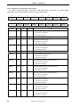
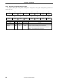
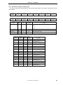
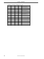
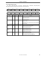
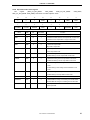
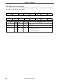
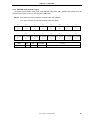
1
To our customers, Old Company Name in Catalogs and Other Documents On April 1st, 2010, NEC Electronics Corporation merged with Renesas Technology Corporation, and Renesas Electronics Corporation took over all the business of both companies. Therefore, although the old company name remains in this document, it is a valid Renesas Electronics document. We appreciate your understanding. Renesas Electronics website: http://www.renesas.com April 1st, 2010 Renesas Electronics Corporation Issued by: Renesas Electronics Corporation (http://www.renesas.com) Send any inquiries to http://www.renesas.com/inquiry. Notice 1. 2. 3. 4. 5. 6. 7. All information included in this document is current as of the date this document is issued. Such information, however, is subject to change without any prior notice. Before purchasing or using any Renesas Electronics products listed herein, please confirm the latest product information with a Renesas Electronics sales office. Also, please pay regular and careful attention to additional and different information to be disclosed by Renesas Electronics such as that disclosed through our website. Renesas Electronics does not assume any liability for infringement of patents, copyrights, or other intellectual property rights of third parties by or arising from the use of Renesas Electronics products or technical information described in this document. No license, express, implied or otherwise, is granted hereby under any patents, copyrights or other intellectual property rights of Renesas Electronics or others. You should not alter, modify, copy, or otherwise misappropriate any Renesas Electronics product, whether in whole or in part. Descriptions of circuits, software and other related information in this document are provided only to illustrate the operation of semiconductor products and application examples. You are fully responsible for the incorporation of these circuits, software, and information in the design of your equipment. Renesas Electronics assumes no responsibility for any losses incurred by you or third parties arising from the use of these circuits, software, or information. When exporting the products or technology described in this document, you should comply with the applicable export control laws and regulations and follow the procedures required by such laws and regulations. You should not use Renesas Electronics products or the technology described in this document for any purpose relating to military applications or use by the military, including but not limited to the development of weapons of mass destruction. Renesas Electronics products and technology may not be used for or incorporated into any products or systems whose manufacture, use, or sale is prohibited under any applicable domestic or foreign laws or regulations. Renesas Electronics has used reasonable care in preparing the information included in this document, but Renesas Electronics does not warrant that such information is error free. Renesas Electronics assumes no liability whatsoever for any damages incurred by you resulting from errors in or omissions from the information included herein. Renesas Electronics products are classified according to the following three quality grades: “Standard”, “High Quality”, and “Specific”. The recommended applications for each Renesas Electronics product depends on the product’s quality grade, as indicated below. You must check the quality grade of each Renesas Electronics product before using it in a particular application. You may not use any Renesas Electronics product for any application categorized as “Specific” without the prior written consent of Renesas Electronics. Further, you may not use any Renesas Electronics product for any application for which it is not intended without the prior written consent of Renesas Electronics. Renesas Electronics shall not be in any way liable for any damages or losses incurred by you or third parties arising from the use of any Renesas Electronics product for an application categorized as “Specific” or for which the product is not intended where you have failed to obtain the prior written consent of Renesas Electronics. The quality grade of each Renesas Electronics product is “Standard” unless otherwise expressly specified in a Renesas Electronics data sheets or data books, etc. “Standard”: 8. 9. 10. 11. 12. Computers; office equipment; communications equipment; test and measurement equipment; audio and visual equipment; home electronic appliances; machine tools; personal electronic equipment; and industrial robots. “High Quality”: Transportation equipment (automobiles, trains, ships, etc.); traffic control systems; anti-disaster systems; anticrime systems; safety equipment; and medical equipment not specifically designed for life support. “Specific”: Aircraft; aerospace equipment; submersible repeaters; nuclear reactor control systems; medical equipment or systems for life support (e.g. artificial life support devices or systems), surgical implantations, or healthcare intervention (e.g. excision, etc.), and any other applications or purposes that pose a direct threat to human life. You should use the Renesas Electronics products described in this document within the range specified by Renesas Electronics, especially with respect to the maximum rating, operating supply voltage range, movement power voltage range, heat radiation characteristics, installation and other product characteristics. Renesas Electronics shall have no liability for malfunctions or damages arising out of the use of Renesas Electronics products beyond such specified ranges. Although Renesas Electronics endeavors to improve the quality and reliability of its products, semiconductor products have specific characteristics such as the occurrence of failure at a certain rate and malfunctions under certain use conditions. Further, Renesas Electronics products are not subject to radiation resistance design. Please be sure to implement safety measures to guard them against the possibility of physical injury, and injury or damage caused by fire in the event of the failure of a Renesas Electronics product, such as safety design for hardware and software including but not limited to redundancy, fire control and malfunction prevention, appropriate treatment for aging degradation or any other appropriate measures. Because the evaluation of microcomputer software alone is very difficult, please evaluate the safety of the final products or system manufactured by you. Please contact a Renesas Electronics sales office for details as to environmental matters such as the environmental compatibility of each Renesas Electronics product. Please use Renesas Electronics products in compliance with all applicable laws and regulations that regulate the inclusion or use of controlled substances, including without limitation, the EU RoHS Directive. Renesas Electronics assumes no liability for damages or losses occurring as a result of your noncompliance with applicable laws and regulations. This document may not be reproduced or duplicated, in any form, in whole or in part, without prior written consent of Renesas Electronics. Please contact a Renesas Electronics sales office if you have any questions regarding the information contained in this document or Renesas Electronics products, or if you have any other inquiries. (Note 1) “Renesas Electronics” as used in this document means Renesas Electronics Corporation and also includes its majorityowned subsidiaries. (Note 2) “Renesas Electronics product(s)” means any product developed or manufactured by or for Renesas Electronics. User’s Manual Multimedia Processor for Mobile Applications SD Memory Card Interface EMMA MobileTM1 Document No. S19361EJ4V0UM00 (4th edition) Date Published September 2009 2009 Printed in Japan [MEMO] 2 User’s Manual S19361EJ4V0UM NOTES FOR CMOS DEVICES 1 VOLTAGE APPLICATION WAVEFORM AT INPUT PIN Waveform distortion due to input noise or a reflected wave may cause malfunction. If the input of the CMOS device stays in the area between VIL (MAX) and VIH (MIN) due to noise, etc., the device may malfunction. Take care to prevent chattering noise from entering the device when the input level is fixed, and also in the transition period when the input level passes through the area between VIL (MAX) and VIH (MIN). 2 HANDLING OF UNUSED INPUT PINS Unconnected CMOS device inputs can be cause of malfunction. If an input pin is unconnected, it is possible that an internal input level may be generated due to noise, etc., causing malfunction. CMOS devices behave differently than Bipolar or NMOS devices. Input levels of CMOS devices must be fixed high or low by using pull-up or pull-down circuitry. Each unused pin should be connected to VDD or GND via a resistor if there is a possibility that it will be an output pin. All handling related to unused pins must be judged separately for each device and according to related specifications governing the device. 3 PRECAUTION AGAINST ESD A strong electric field, when exposed to a MOS device, can cause destruction of the gate oxide and ultimately degrade the device operation. Steps must be taken to stop generation of static electricity as much as possible, and quickly dissipate it when it has occurred. Environmental control must be adequate. When it is dry, a humidifier should be used. It is recommended to avoid using insulators that easily build up static electricity. Semiconductor devices must be stored and transported in an anti-static container, static shielding bag or conductive material. All test and measurement tools including work benches and floors should be grounded. The operator should be grounded using a wrist strap. Semiconductor devices must not be touched with bare hands. Similar precautions need to be taken for PW boards with mounted semiconductor devices. 4 STATUS BEFORE INITIALIZATION Power-on does not necessarily define the initial status of a MOS device. Immediately after the power source is turned ON, devices with reset functions have not yet been initialized. Hence, power-on does not guarantee output pin levels, I/O settings or contents of registers. A device is not initialized until the reset signal is received. A reset operation must be executed immediately after power-on for devices with reset functions. 5 POWER ON/OFF SEQUENCE In the case of a device that uses different power supplies for the internal operation and external interface, as a rule, switch on the external power supply after switching on the internal power supply. When switching the power supply off, as a rule, switch off the external power supply and then the internal power supply. Use of the reverse power on/off sequences may result in the application of an overvoltage to the internal elements of the device, causing malfunction and degradation of internal elements due to the passage of an abnormal current. The correct power on/off sequence must be judged separately for each device and according to related specifications governing the device. 6 INPUT OF SIGNAL DURING POWER OFF STATE Do not input signals or an I/O pull-up power supply while the device is not powered. The current injection that results from input of such a signal or I/O pull-up power supply may cause malfunction and the abnormal current that passes in the device at this time may cause degradation of internal elements. Input of signals during the power off state must be judged separately for each device and according to related specifications governing the device. User’s Manual S19361EJ4V0UM 3 The names of other companies and products are the registered trademarks or trademarks of the respective company. • The information in this document is current as of September, 2009. The information is subject to change without notice. For actual design-in, refer to the latest publications of NEC Electronics data sheets, etc., for the most up-to-date specifications of NEC Electronics products. Not all products and/or types are available in every country. Please check with an NEC Electronics sales representative for availability and additional information. • No part of this document may be copied or reproduced in any form or by any means without the prior written consent of NEC Electronics. NEC Electronics assumes no responsibility for any errors that may appear in this document. • NEC Electronics does not assume any liability for infringement of patents, copyrights or other intellectual property rights of third parties by or arising from the use of NEC Electronics products listed in this document or any other liability arising from the use of such products. No license, express, implied or otherwise, is granted under any patents, copyrights or other intellectual property rights of NEC Electronics or others. • Descriptions of circuits, software and other related information in this document are provided for illustrative purposes in semiconductor product operation and application examples. The incorporation of these circuits, software and information in the design of a customer's equipment shall be done under the full responsibility of the customer. NEC Electronics assumes no responsibility for any losses incurred by customers or third parties arising from the use of these circuits, software and information. • While NEC Electronics endeavors to enhance the quality and safety of NEC Electronics products, customers agree and acknowledge that the possibility of defects thereof cannot be eliminated entirely. In addition, NEC Electronics products are not taken measures to prevent radioactive rays in the product design. When customers use NEC Electronics products with their products, customers shall, on their own responsibility, incorporate sufficient safety measures such as redundancy, fire-containment and anti-failure features to their products in order to avoid risks of the damages to property (including public or social property) or injury (including death) to persons, as the result of defects of NEC Electronics products. • NEC Electronics products are classified into the following three quality grades: "Standard", "Special" and "Specific". The "Specific" quality grade applies only to NEC Electronics products developed based on a customerdesignated "quality assurance program" for a specific application. The recommended applications of an NEC Electronics product depend on its quality grade, as indicated below. Customers must check the quality grade of each NEC Electronics product before using it in a particular application. "Standard": Computers, office equipment, communications equipment, test and measurement equipment, audio and visual equipment, home electronic appliances, machine tools, personal electronic equipment and industrial robots. "Special": Transportation equipment (automobiles, trains, ships, etc.), traffic control systems, anti-disaster systems, anti-crime systems, safety equipment and medical equipment (not specifically designed for life support). "Specific": Aircraft, aerospace equipment, submersible repeaters, nuclear reactor control systems, life support systems and medical equipment for life support, etc. The quality grade of NEC Electronics products is "Standard" unless otherwise expressly specified in NEC Electronics data sheets or data books, etc. If customers wish to use NEC Electronics products in applications not intended by NEC Electronics, they must contact an NEC Electronics sales representative in advance to determine NEC Electronics' willingness to support a given application. (Note) (1) "NEC Electronics" as used in this statement means NEC Electronics Corporation and also includes its majority-owned subsidiaries. (2) "NEC Electronics products" means any product developed or manufactured by or for NEC Electronics (as defined above). M8E0904E 4 User’s Manual S19361EJ4V0UM PREFACE Readers This manual is intended for hardware/software application system designers who wish to understand and use the SD card interface functions of EMMA Mobile1 (EM1), a multimedia processor for mobile applications. Purpose This manual is intended to explain to users the hardware and software functions of the SD card interface of EM1, and be used as a reference material for developing hardware and software for systems that use EM1. Organization How to Read This Manual This manual consists of the following chapters. Chapter 1 Overview Chapter 2 Pin functions Chapter 3 Registers Chapter 4 Description of functions It is assumed that the readers of this manual have general knowledge of electricity, logic circuits, and microcontrollers. To understand the functions of the SD card interface of EM1 in detail Read this manual according to the CONTENTS. To understand the other functions of EM1 Refer to the user’s manual of the respective module. To understand the electrical specifications of EM1 Conventions Refer to the Data Sheet. Data significance: Higher digits on the left and lower digits on the right Note: Footnote for item marked with Note in the text Caution: Information requiring particular attention Remark: Supplementary information Numeric representation: Binary ... xxxx or xxxxB Decimal ... xxxx Hexadecimal ... xxxxh Data type: Word … 32 bits Halfword … 16 bits Byte User’s Manual S19361EJ4V0UM … 8 bits 5 Related Documents The related documents indicated in this publication may include preliminary versions. However, preliminary versions are not marked as such. Document Name Document No. MC-10118A Data sheet S19657E PD77630A Data sheet S19686E User’s manual Audio/Voice and PWM Interfaces S19253E DDR SDRAM Interface S19254E DMA Controller S19255E 2 Caution I C Interface S19256E ITU-R BT.656 Interface S19257E LCD Controller S19258E MICROWIRE S19259E NAND Flash Interface S19260E SPI S19261E UART Interface S19262E Image Composer S19263E Image Processor Unit S19264E System Control/General-Purpose I/O Interface S19265E Timer S19266E Terrestrial Digital TV Interface S19267E Camera Interface S19285E USB Interface S19359E SD Memory Card Interface This manual PDMA S19373E One Chip (MC-10118A) S19598E One Chip (PD77630A) S19687E The related documents listed above are subject to change without notice. Be sure to use the latest version of each document when designing. 6 User’s Manual S19361EJ4V0UM CONTENTS CHAPTER 1 OVERVIEW............................................................................................................................9 1.1 Features .......................................................................................................................................9 CHAPTER 2 PIN FUNCTIONS ................................................................................................................10 2.1 SD Card Interface Pins .............................................................................................................10 CHAPTER 3 REGISTERS ........................................................................................................................11 3.1 3.2 Registers....................................................................................................................................11 Register Functions ...................................................................................................................13 3.2.1 3.2.2 3.2.3 3.2.4 3.2.5 3.2.6 3.2.7 3.2.8 3.2.9 3.2.10 3.2.11 3.2.12 3.2.13 3.2.14 3.2.15 3.2.16 3.2.17 3.2.18 3.2.19 3.2.20 3.2.21 3.2.22 3.2.23 3.2.24 3.2.25 3.2.26 3.2.27 3.2.28 3.2.29 3.2.30 3.2.31 3.2.32 SD memory card command register .............................................................................................13 SD memory card port select register............................................................................................. 15 SD memory card command parameter register 0 .........................................................................16 SD memory card command parameter register 1 .........................................................................16 SD memory card stop register ...................................................................................................... 17 SD memory card transfer sector count register.............................................................................17 SD memory card response register 0 ...........................................................................................18 SD memory card response register 1 ...........................................................................................18 SD memory card response register 2 ...........................................................................................19 SD memory card response register 3 ...........................................................................................19 SD memory card response register 4 ...........................................................................................20 SD memory card response register 5 ...........................................................................................20 SD memory card response register 6 ...........................................................................................21 SD memory card response register 7 ...........................................................................................21 SD memory card information register 1 ........................................................................................22 SD memory card information register 2 ........................................................................................23 SD memory card information mask register 1 ...............................................................................25 SD memory card information mask register 2 ...............................................................................26 SD memory card transfer clock control register ............................................................................27 SD memory card transfer data size register..................................................................................28 SD memory card option setting register ........................................................................................29 SD memory card error interrupt status register 1 ..........................................................................31 SD memory card error interrupt status register 2 ..........................................................................33 SD memory card data buffer 0 register .........................................................................................34 SDIO mode setting register........................................................................................................... 34 SDIO information register.............................................................................................................. 35 SDIO information mask register .................................................................................................... 36 Expansion mode control register................................................................................................... 37 SDIx software reset control register .............................................................................................. 38 SDIx use register ..........................................................................................................................39 SDIx use register 2 .......................................................................................................................40 SDIx DMA mode SD buffer register ..............................................................................................41 CHAPTER 4 DESCRIPTION OF FUNCTIONS ......................................................................................42 4.1 4.2 Selecting SD Memory Card Transfer Clock Signal (in Synchronous Mode) ......................42 SDIO Interrupts..........................................................................................................................42 User’s Manual S19361EJ4V0UM 7 LIST OF FIGURES Figure No. Title Page 4-1. SDIO Interrupt Timing When SDIA Is Used in 1-Bit Mode ................................................................................... 43 4-2. SDIO Interrupt Timing When SDIA Is Used in 4-Bit Mode (When Single Block Transfer Command Is Used) ..... 43 4-3. SDIO Interrupt Timing When SDIA Is Used in 4-Bit Mode (When Multiple Block Transfer Command Is Used)... 44 LIST OF TABLES Table No. Title Page 4-1. SD Memory Card Transfer Clock Signals That Can Be Selected (in Asynchronous Mode)................................. 42 8 User’s Manual S19361EJ4V0UM CHAPTER 1 OVERVIEW This manual describes the functional specifications of the modules related to the SDIO card and non-secure SD memory card interfaces (SDIA, SDIB, and SDIC, which are represented as SDIx below) provided in EM1. 1.1 Features The main features of SDIx are as follows. Supports a line width of 1 bit or 4 bits for transferring data to and from SD memory cards or SDIO cards. Supports data transfers in frame units. Supports CRC7 error checks on the command line and CRC16 checks (hardware) on each data bit line. Provides three SD memory card and SDIO card ports. The data transfer buffer for SD memory cards is configured of two blocks of 16 bits 256 words. Supports data transfers from 1 to 512 bytes. The SD memory card transfer clock signal can be derived from the source clock signal in the SDIx module (by selecting to divide the source clock frequency by 2, 4, 8, 16, …, or 512). Supports SD Specifications Part 1 Physical Layer Simplified Specification Ver. 2.0, SDIO Physical Specifications 2.0, and specifications equivalent to MMC 4.2. User’s Manual S19361EJ4V0UM 9 CHAPTER 2 PIN FUNCTIONS 2.1 SD Card Interface Pins Pin Name I/O After Reset SD0_CKO Output 0 Clock output - SD0_CMD I/O 0 Command - SD0_DATA0 I/O 0 Data - SD0_DATA1 I/O 0 Data GIO_P88 SD0_DATA2 I/O 0 Data GIO_P89 SD0_DATA3 I/O 0 Data GIO_P90 SD0_CKI Input Clock input GIO_P91 SD1_CKO Output 0 Clock output SD1_CMD I/O 0 Command CAM_YUV5 SD1_DATA0 I/O 0 Data CAM_YUV6 SD1_DATA1 I/O 0 Data CAM_YUV7 SD1_DATA2 I/O 0 Data CAM_VS SD1_DATA3 I/O 0 Data CAM_HS SD1_CKI Input Clock input GIO_P92, CAM_CLKI SD2_CKO Output 0 Clock output GIO_P112, NAND_D2 SD2_CMD I/O 0 Command GIO_P113, NAND_D3 SD2_DATA0 I/O 0 Data GIO_P114, NAND_D4 SD2_DATA1 I/O 0 Data GIO_P115, NAND_D5 SD2_DATA2 I/O 0 Data GIO_P116, NAND_D6 SD2_DATA3 I/O 0 Data GIO_P117, NAND_D7 SD2_CKI Input Clock input GIO_P93, NAND_OE 10 Function User’s Manual S19361EJ4V0UM Alternate Pin Function CHAPTER 3 REGISTERS 3.1 Registers The registers that control SDIx consist of 16 bits. The registers are accessed from the ACPU, ADSP, and DMAC in word (32-bit) units, of which the higher 16 bits are invalid data. Invalid data means that the data written is ignored and the data read is 0. Do not access reserved registers. Do not write any value other than 0 to reserved bits in each register. Base addresses: SD0 (SDIA) 5005_0000H SD1 (SDIB) 5006_0000H SD2 (SDIC) 5009_0000H (1/2) Address Register Name Register Symbol R/W After Reset 500x_0000h SD memory card command register SDIx_CMD R/W 0000_0000h 500x_0004h SD memory card port select register SDIx_PORT R/W 0000_0100h 500x_0008h SD memory card command parameter register 0 SDIx_ARG0 R/W 0000_0000h 500x_000Ch SD memory card command parameter register 1 SDIx_ARG1 R/W 0000_0000h 500x_0010h SD memory card stop register SDIx_STOP R/W 0000_0000h 500x_0014h SD memory card transfer sector count register SDIx_SECCNT R/W 0000_0000h 500x_0018h SD memory card response register 0 SDIx_RSP0 R 0000_0000h 500x_001Ch SD memory card response register 1 SDIx_RSP1 R 0000_0000h 500x_0020h SD memory card response register 2 SDIx_RSP2 R 0000_0000h 500x_0024h SD memory card response register 3 SDIx_RSP3 R 0000_0000h 500x_0028h SD memory card response register 4 SDIx_RSP4 R 0000_0000h 500x_002Ch SD memory card response register 5 SDIx_RSP5 R 0000_0000h 500x_0030h SD memory card response register 6 SDIx_RSP6 R 0000_0000h 500x_0034h SD memory card response register 7 SDIx_RSP7 R 0000_0000h 500x_0038h SD memory card information register 1 SDIx_INFO1 R/W, R Undefined (0000_068D) 500x_003Ch SD memory card information register 2 SDIx_INFO2 R/W, R Undefined (0000_2080h) 500x_0040h SD memory card information mask register 1 SDIx_INFO1_MASK R/W 0000_031Dh 500x_0044h SD memory card information mask register 2 SDIx_INFO2_MASK R/W 0000_8B7Fh 500x_0048h SD memory card transfer clock control register SDIx_CLK_CTRL R/W 0000_0020h 500x_004Ch SD memory card transfer data size register SDIx_SIZE R/W 0000_0200h 500x_0050h SD memory card option setting register SDIx_OPTION R/W 0000_00EEh 500x_0054h Reserved 500x_0058h SD memory card error interrupt status register 1 SDIx_ERR_STS1 R 0000_2000h 500x_005Ch SD memory card error interrupt status register 2 SDIx_ERR_STS2 R 0000_0000h User’s Manual S19361EJ4V0UM 11 CHAPTER 3 REGISTERS (2/2) Address Register Name Register Symbol SDIx_BUF0 R/W After Reset R/W Undefined 500x_0060h SD memory card data buffer 0 register 500x_0064h Reserved 500x_0068h SDIO mode setting register SDIx_SDIO_MODE R/W 0000_0000h 500x_006Ch SDIO information register SDIx_SDIO_INFO1 R/W 0000_0000h 500x_0070h SDIO information mask register SDIx_SDIO_INFO1_ R/W 0000_C007h MASK 500x_0074h to Reserved 500x_01ACh 500x_01B0h Expansion mode control register 500x_01B4h Reserved SDIx_CC_EXT_MODE R, R/W 0000_1000h R/W 0000_0000h 500x_01BCh 500x_01C0h SDIx software reset control register SDIx_SOFT_RST 500x_01C4h to Reserved 500x_01E0h 500x_0200h SDIx use register SDIx_USER R/W, R 0000_0004h 500x_0204h SDIx use register 2 SDIx_USER2 R/W 0000_0000h R/W 500x_0210h to Reserved 500x_02FCh 500x_0300h 12 SDIx DMA mode SD buffer register SDIx_DMASD User’s Manual S19361EJ4V0UM CHAPTER 3 REGISTERS 3.2 Register Functions 3.2.1 SD memory card command register This register (SDIA_CMD: 5005_0000h, SDIB_CMD: 5006_000h, SDIC_CMD: 5009_000h) controls the SD memory card commands and responses. 15 14 13 12 11 10 9 8 MD7 MD6 MD5 MD4 MD3 MD2 MD1 MD0 7 6 5 4 3 2 1 0 C1 C0 CF45 CF44 CF43 CF42 CF41 CF40 Name R/W Bit After Reset Function MD[7:6] R/W 15:14 0 Specifies the CMD12 mode. MD5 R/W 13 0 Selects between single- or multiple-block transfers. 0: Single-block transfer 1: Multiple-block transfer MD4 R/W 12 0 Specifies the write or read mode. 0: Write 1: Read MD3 R/W 11 0 Specifies the data mode. 0: No data 1: Data is present MD[2:0] R/W 10:8 0 Specifies an expansion command and the response type. C[1:0] R/W 7:6 0 Specifies the command mode. CF[45:40] R/W 5:0 0 Specifies the command index. Caution For details about setup commands and responses, see SD Specifications Part 1 Physical Layer Simplified Specification Ver. 2.0. MD[7:6] CMD12 mode specification MD7 MD6 0 0 Automatic CMD12 transfer 0 1 Non-automatic transfer of CMD12 (SDIO command) (transfer between host and SD card) 1 0 Reserved 1 1 Reserved Remark Function Automatic CMD12 transfer means that CMD12 is automatically transferred according to the sector count, after which data transfer stops. User’s Manual S19361EJ4V0UM 13 CHAPTER 3 REGISTERS MD[2:0] Expansion command and response type specification MD2 MD1 MD0 0 0 0 Command Mode Response Type Normal mode Decoding command for SD memory cards and multimedia cards 0 0 1 Expansion command Reserved 0 1 0 Expansion command Reserved 0 1 1 Expansion command No response 1 0 0 Expansion command R1, R6, R5 1 0 1 Expansion command R1b, R5b 1 1 0 Expansion command R2 1 1 1 Expansion command R3, R4 C[1:0] Command mode specification C1 C0 Function 0 0 SD memory card or multimedia card command 0 1 ACMD following CMD55 of an SD memory card 1 0 Mutual recognition command 1 1 Reserved CF[45:40] Command index specification Specifies the command index set to bits 45 to 40 in the SD memory card command format. 14 5 4 3 2 1 0 CF45 CF44 CF43 CF42 CF41 CF40 User’s Manual S19361EJ4V0UM CHAPTER 3 REGISTERS 3.2.2 SD memory card port select register This register (SDIA_PORT: 5005_0004h, SDIB_PORT: 5006_0004h, SDIC_PORT: 5009_0004h) specifies the port used when multiple SD memory card ports are mounted. 15 14 13 12 11 Reserved 7 6 5 4 3 10 9 8 NP2 NP1 NP0 2 1 0 P1 P0 Reserved Name R/W Bit After Reset Function Reserved 15:11 NP[2:0] R 10:8 1 Reserved 7:2 R/W 1:0 0 P[1:0] Specifies the number of supported SD memory cards. Selects the port number of the selected SD memory card. NP[2:0] Number of supported SD memory cards NP2 NP1 NP0 Function 0 0 0 Not defined 0 0 1 1 port (default) 0 1 0 2 ports 0 1 1 3 ports 1 0 0 4 ports P[1:0] Port number of the selected SD memory card P1 P0 Function 0 0 Port 0 0 1 Setting prohibitedNote 1 0 Setting prohibitedNote 1 1 Setting prohibitedNote Note Operation is not guaranteed if a value other than 0 is specified for bits P1 and P0. User’s Manual S19361EJ4V0UM 15 CHAPTER 3 REGISTERS 3.2.3 SD memory card command parameter register 0 This register (SDIA_ARG0: 5005_0008h, SDIB_ARG0: 5006_0008h, SDIC_ARG0: 5009_0008h) stores the SD card command parameters. 15 14 13 12 11 10 9 8 CF23 CF22 CF21 CF20 CF19 CF18 CF17 CF16 7 6 5 4 3 2 1 0 CF15 CF14 CF13 CF12 CF11 CF10 CF9 CF8 Name CF[23:8] R/W Bit After Reset R/W 15:0 0x0000 Function Specifies the parameters for the command to be transferred to the SD memory card. The settings of these bits correspond to bits 23 to 8 of the command format. Remark For details about the command parameters, see SD Specifications Part 1 Physical Layer Simplified Specification Ver. 2.0. 3.2.4 SD memory card command parameter register 1 This register (SDIA_ARG1: 5005_000Ch, SDIB_ARG1: 5006_000Ch, SDIC_ARG1: 5009_000Ch) stores the SD card command parameters. 15 14 13 12 11 10 9 8 CF39 CF38 CF37 CF36 CF35 CF34 CF33 CF32 7 6 5 4 3 2 1 0 CF31 CF30 CF29 CF28 CF27 CF26 CF25 CF24 Name CF[39:24] R/W Bit After Reset R/W 15:0 0x0000 Function Specifies the parameters for the command to be transferred to the SD memory card. The settings of these bits correspond to bits 39 to 24 of the command format. Remark For details about the command parameters, see SD Specifications Part 1 Physical Layer Simplified Specification Ver. 2.0. 16 User’s Manual S19361EJ4V0UM CHAPTER 3 REGISTERS 3.2.5 SD memory card stop register This register (SDIA_STOP: 5005_0010h, SDIB_STOP: 5006_0010h, SDIC_STOP: 5009_0010h) specifies stopping SD transfers. 15 14 13 12 11 10 9 8 0 0 0 0 0 0 0 SEC 7 6 5 4 3 2 1 0 0 0 0 0 0 0 0 STP Name R/W Bit After Reset Function 15:9 0 R/W 8 0 Reserved SEC Enables or disables the SDIx_SECCNT register. 0: Disables the SDIx_SECCNT register. 1: Enables the SDIx_SECCNT register. 7:1 0 R/W 0 0 Reserved STP Transfer stop bit 0: Do not stop transfer. Set this bit to 0 before CMD17, CMD18, CMD24, CMD27, CMD30, CMD42, CMD56, CMD43 to CMD48, ACMD18, or ACMD25 is set. 1: Stop transfer. 3.2.6 SD memory card transfer sector count register This register (SDIA_SECCNT: 5005_0014h, SDIB_SECCNT: 5006_0014h, SDIC_SECCNT: 5009_0014h) counts the number of transfer sectors. 15 14 13 12 11 10 9 8 CNT15 CNT14 CNT13 CNT12 CNT11 CNT10 CNT9 CNT8 7 6 5 4 3 2 1 0 CNT7 CNT6 CNT5 CNT4 CNT3 CNT2 CNT1 CNT0 Name CNT[15:0] Remark R/W Bit After Reset R/W 15:0 0x0000 Function 16-bit counter that counts the number of transfer sectors If SDIx_SECCNT is 0x0001, the number of transfer sectors is 1. If SDIx_SECCNT is 0xFFFF, the number of transfer sectors is 65,535. if SDIx_SECCNT is 0x0000, the number of transfer sectors is 65,536. User’s Manual S19361EJ4V0UM 17 CHAPTER 3 REGISTERS 3.2.7 SD memory card response register 0 This register (SDIA_RSP0: 5005_0018h, SDIB_RSP0: 5006_0018h, SDIC_RSP0: 5009_0018h) stores the responses returned from the SD memory card. 15 14 13 12 11 10 9 8 R23 R22 R21 R20 R19 R18 R17 R16 7 6 5 4 3 2 1 0 R15 R14 R13 R12 R11 R10 R9 R8 Name R/W Bit After Reset R 15:0 0x0000 R[23:8] Function Stores the responses returned from the SD memory card. The settings of these bits correspond to bits 23 to 8 of the response format. Remark For details about the response formats, see SD Specifications Part 1 Physical Layer Simplified Specification Ver. 2.0. 3.2.8 SD memory card response register 1 This register (SDIA_RSP1: 5005_001Ch, SDIB_RSP1: 5006_001Ch, SDIC_RSP1: 5009_001Ch) stores the responses returned from the SD memory card. 15 14 13 12 11 10 9 8 R39 R38 R37 R36 R35 R34 R33 R32 7 6 5 4 3 2 1 0 R31 R30 R29 R28 R27 R26 R25 R24 Name R[39:24] R/W Bit After Reset R 15:0 0x0000 Function Stores the responses returned from the SD memory card. The settings of these bits correspond to bits 39 to 24 of the response format. Remark For details about the response formats, see SD Specifications Part 1 Physical Layer Simplified Specification Ver. 2.0. 18 User’s Manual S19361EJ4V0UM CHAPTER 3 REGISTERS 3.2.9 SD memory card response register 2 This register (SDIA_RSP2: 5005_0020h, SDIB_RSP2: 5006_0020h, SDIC_RSP2: 5009_0020h) stores the responses returned from the SD memory card. 15 14 13 12 11 10 9 8 R55 R54 R53 R52 R51 R50 R49 R48 7 6 5 4 3 2 1 0 R47 R46 R45 R44 R43 R42 R41 R40 Name R/W Bit After Reset R 15:0 0x0000 R[55:40] Function Stores the responses returned from the SD memory card. The settings of these bits correspond to bits 55 to 40 of the response format. Remark For details about the response formats, see SD Specifications Part 1 Physical Layer Simplified Specification Ver. 2.0. 3.2.10 SD memory card response register 3 This register (SDIA_RSP3: 5005_0024h, SDIB_RSP3: 5006_0024h, SDIC_RSP3: 5009_0024h) stores the responses returned from the SD memory card. 15 14 13 12 11 10 9 8 R71 R70 R69 R68 R67 R66 R65 R64 7 6 5 4 3 2 1 0 R63 R62 R61 R60 R59 R58 R57 R56 Name R[71:56] R/W Bit After Reset R 15:0 0x0000 Function Stores the responses returned from the SD memory card. The settings of these bits correspond to bits 71 to 56 of the response format. Remark For details about the response formats, see SD Specifications Part 1 Physical Layer Simplified Specification Ver. 2.0. User’s Manual S19361EJ4V0UM 19 CHAPTER 3 REGISTERS 3.2.11 SD memory card response register 4 This register (SDIA_RSP4: 5005_0028h, SDIB_RSP4: 5006_0028h, SDIC_RSP4: 5009_0028h) stores the responses returned from the SD memory card. 15 14 13 12 11 10 9 8 R87 R86 R85 R84 R83 R82 R81 R80 7 6 5 4 3 2 1 0 R79 R78 R77 R76 R75 R74 R73 R72 Name R/W Bit After Reset R 15:0 0x0000 R[87:72] Function Stores the responses returned from the SD memory card. The settings of these bits correspond to bits 87 to 72 of the response format. Remark For details about the response formats, see SD Specifications Part 1 Physical Layer Simplified Specification Ver. 2.0. 3.2.12 SD memory card response register 5 This register (SDIA_RSP5: 5005_002Ch, SDIB_RSP5: 5006_002Ch, SDIC_RSP5: 5009_002Ch) stores the responses returned from the SD memory card. 15 14 13 12 11 10 9 8 R103 R102 R101 R100 R99 R98 R97 R96 7 6 5 4 3 2 1 0 R95 R94 R93 R92 R91 R90 R89 R88 Name R[103:88] R/W Bit After Reset R 15:0 0x0000 Function Stores the responses returned from the SD memory card. The settings of these bits correspond to bits 103 to 88 of the response format. Remark For details about the response formats, see SD Specifications Part 1 Physical Layer Simplified Specification Ver. 2.0. 20 User’s Manual S19361EJ4V0UM CHAPTER 3 REGISTERS 3.2.13 SD memory card response register 6 This register (SDIA_RSP6: 5005_0030h, SDIB_RSP6: 5006_0030h, SDIC_RSP6: 5009_0030h) stores the responses returned from the SD memory card. 15 14 13 12 11 10 9 8 R119 R118 R117 R116 R115 R114 R113 R112 7 6 5 4 3 2 1 0 R111 R110 R109 R108 R107 R106 R105 R104 Name R/W Bit After Reset R 15:0 0x0000 R[119:104] Function Stores the responses returned from the SD memory card. The settings of these bits correspond to bits 119 to 104 of the response format. Remark For details about the response formats, see SD Specifications Part 1 Physical Layer Simplified Specification Ver. 2.0. 3.2.14 SD memory card response register 7 This register (SDIA_RSP7: 5005_0034h, SDIB_RSP7: 5006_0034h, SDIC_RSP7: 5009_0034h) stores the responses returned from the SD memory card. 15 14 13 12 11 10 9 8 0 0 0 0 0 0 0 0 7 6 5 4 3 2 1 0 R127 R126 R125 R124 R123 R122 R121 R120 Name R/W Bit After Reset Function Reserved 15:8 0 R[127:120] R 7:0 0x0000 Stores the responses returned from the SD memory card. The settings of these bits correspond to bits 127 to 120 of the response format. Remark For details about the response formats, see SD Specifications Part 1 Physical Layer Simplified Specification Ver. 2.0. User’s Manual S19361EJ4V0UM 21 CHAPTER 3 REGISTERS 3.2.15 SD memory card information register 1 This register (SDIA_INFO1: 5005_0038h, SDIB_INFO1: 5006_0038h, SDIC_INFO1: 5009_0038h) indicates two of the interrupt sources of SDIx. 15 14 13 12 11 10 9 8 0 0 0 0 0 0 0 0 7 6 5 4 3 2 1 0 0 0 0 0 0 INFO2 0 INFO0 Name R/W Bit After Reset Function 15:3 0 R/W 2 0 Reserved INFO2 Indicates whether all read/write accesses have finished. 0: Not all accesses have finished. 1: All accesses have finished. Reserved INFO0 1 0 R/W 0 0 Indicates whether the response has ended. 0: The response has not ended. 1: The response has ended. 22 User’s Manual S19361EJ4V0UM CHAPTER 3 REGISTERS 3.2.16 SD memory card information register 2 This register (SDIA_INFO2: 5005_003Ch, SDIB_INFO2: 5006_003Ch, SDIC_INFO2: 5009_003Ch) indicates the error and buffer status interrupt sources of SDIx. 15 14 13 12 11 10 9 8 ILA CBSY SCLKDIVEN 0 0 0 BWE BRE 7 6 5 4 3 2 1 0 DAT0 ERR6 ERR5 ERR4 ERR3 ERR2 ERR1 ERR0 (1/2) Name ILA R/W R/W Bit 15 After Reset 0 Function Note 1 Illegal access error 0: Normal access 1: Illegal access error CBSY R 14 0 Command register busy 0: Transfer is complete. 1: Transfer is in progress. SCLKDIVEN R 13 0 SD_CLK_DIV enable bit 0: The SD bus is being used to transmit commands and data. 1: The SD bus is not being used to transmit commands and data. Reserved BWE 12:10 0 R/W 9 0 Write enable 0: Writing to the SD memory card is disabled. 1: Writing to the SD memory card is enabled. (The data buffer in SDIx is empty.) BRE R/W 8 0 Read enable 0: Reading from the SD memory card is disabled. 1: Reading from the SD memory card is enabled. (The data buffer in SDIx is full.) DAT0 R 7 Undefined SD data line 0 bit 0: SDDATA0 = 0 1: SDDATA0 = 1 ERR6 R/W 6 0 Response timeout 0: No response timeout error occurred. 1: A response timeout error occurred (because no command response or SD_STOP response was issued for 64 SD transfer clock cycles or more). ERR5 R/W 5 0 Invalid data buffer read error bit 0: No invalid data buffer read error occurred. 1: An invalid data buffer read error occurred (because an attempt was made to read data from the data buffer even though the data buffer was empty). User’s Manual S19361EJ4V0UM 23 CHAPTER 3 REGISTERS (2/2) Name ERR4 R/W Bit After Reset R/W 4 0 Function Invalid data buffer write error bit 0: No invalid data buffer write error occurred. 1: An invalid data buffer write error occurredNote 2. ERR3 R/W 3 0 Timeout (other than a response) error 0: No timeout error occurred. 1: A timeout error occurredNote 3. ERR2 R/W 2 0 End error status bit 0: No end error occurred. 1: An end error occurredNote 4. ERR1 R/W 1 0 CRC error status bit 0: No CRC error occurred. 1: A CRC error occurredNote 5. ERR0 R/W 0 0 Command error status bit 0: No command error occurred. 1: A command error occurredNote 6. Remark For details about the response formats, see SD Specifications Part 1 Physical Layer Simplified Specification Ver. 2.0. Notes 1. This error occurs in any of the following cases: If the command register is rewritten during a transfer. If “No response” (MD[2:0] = 011) and “Data is present” (MD3 = 1) is specified in the SDIx_CMD register. If CMD12 for which data is present is specified in the SDIx_CMD register. 2. This error occurs in any of the following cases: If data is written to data buffer SDIx_BUF0 when the data read or data write command status is not asserted. If data is written before SDIx_BUF0 becomes empty during a single block write. If data is written to bank 1 of the data buffer before the bank becomes empty during a multiple block write. 3. This error occurs in any of the following five cases: If SDDAT0 is 0 (busy) for a longer period of time than the number of cycles specified by bits 7 to 4 of the SDIx_OPTION register after an R1b response is received. If SDDAT0 is 0 (busy) for a longer period of time than the number of cycles specified by bits 7 to 4 of the SDIx_OPTION register after the CRC status is written. If the CRC status is not written for a longer period of time than the number of cycles specified by bits 7 to 4 of the SDIx_OPTION register after a write access. If SDDAT0 is 0 (busy) for a longer period of time than the number of cycles specified by bits 7 to 4 of the SDIx_OPTION register after a read command is issued. If SDDAT0 is 0 (busy) for a longer period of time than the number of cycles specified by bits 7 to 4 of the SDIx_OPTION register after an SD_STOP response is issued. 4. End error refers to an END bit error in a command response (response length), in the data read (data length), when the CRC status is written (CRC status length), or in an SD_STOP response. 5. CRC error refers to a CRC status write error, a CRC16 error in the data read, a CRC7 error in a stop response, or a CRC7 error in a response. 6. Command error refers to a command index error in a command response or in an SD_STOP response. 24 User’s Manual S19361EJ4V0UM CHAPTER 3 REGISTERS 3.2.17 SD memory card information mask register 1 This register (SDIA_INFO1_MASK: 5005_0040h, SDIB_INFO1_MASK: 5006_0040h, SDIC_INFO1_MASK: 5009_0040h) masks the SDIx interrupts specified in the SDIx_INFO1 register. 15 14 13 12 11 10 9 8 0 0 0 0 0 0 0 0 7 6 5 4 3 2 1 0 0 0 0 0 0 IMASK2 0 IMASK0 Name R/W Bit After Reset Function 15:3 0 R/W 2 1 Masks the interrupt that detects whether all read/write accesses Reserved IMASK2 have finished. 0: The interrupt is not masked. 1: The interrupt is masked. Reserved IMASK0 1 0 R/W 0 1 Masks the interrupt that detects whether the response has ended. 0: The interrupt is not masked. 1: The interrupt is masked. User’s Manual S19361EJ4V0UM 25 CHAPTER 3 REGISTERS 3.2.18 SD memory card information mask register 2 This register (SDIA_INFO2_MASK: 5005_0044h, SDIB_INFO2_MASK: 5006_0044h, SDIC_INFO2_MASK: 5009_0044h) masks the SDIx interrupts specified in the SDIx_INFO2 register. 15 14 13 12 11 10 9 8 IMASK 0 0 0 0 0 BMSK1 BMSK0 7 6 5 4 3 2 1 0 0 EMASK6 EMASK5 EMASK4 EMASK3 EMASK2 EMASK1 EMASK0 Name IMASK R/W Bit After Reset R/W 15 1 Function Masks the illegal access interrupt. 0: The interrupt is not masked. 1: The interrupt is masked. Reserved 14:10 0 BMASK1 R/W 9 1 Masks the write enable interrupt. 0: The interrupt is not masked. 1: The interrupt is masked. BMASK0 R/W 8 1 Masks the read enable interrupt. 0: The interrupt is not masked. 1: The interrupt is masked. Reserved 7 0 EMASK6 R/W 6 1 Masks the response timeout interrupt. 0: The interrupt is not masked. 1: The interrupt is masked. EMASK5 R/W 5 1 Masks the illegal data buffer read access interrupt. 0: The interrupt is not masked. 1: The interrupt is masked. EMASK4 R/W 4 1 Masks the illegal data buffer write access interrupt. 0: The interrupt is not masked. 1: The interrupt is masked. EMASK3 R/W 3 1 Masks the timeout (other than response) interrupt. 0: The interrupt is not masked. 1: The interrupt is masked. EMASK2 R/W 2 1 Masks the end error interrupt. 0: The interrupt is not masked. 1: The interrupt is masked. EMASK1 R/W 1 1 Masks the CRC error interrupt. 0: The interrupt is not masked. 1: The interrupt is masked. EMASK0 R/W 0 1 Masks the command error interrupt. 0: The interrupt is not masked. 1: The interrupt is masked. 26 User’s Manual S19361EJ4V0UM CHAPTER 3 REGISTERS 3.2.19 SD memory card transfer clock control register This register (SDIA_CLK_CTRL: 5005_0048h, SDIB_CLK_CTRL: 5006_0048h, SDIC_CLK_CTRL: 5009_0048h) specifies the ratio for dividing the SD memory card transfer clock frequency. 15 14 13 12 11 10 9 8 0 0 0 0 0 SDCLKSEL SDCLKOFFEN SCLKEN 7 6 5 4 3 2 1 0 DIV7 DIV6 DIV5 DIV4 DIV3 DIV2 DIV1 DIV0 Name R/W Bit After Reset Function 15:11 0 R/W 10 0 Reserved SDCLKSEL Selects the type of SD memory card according to the transfer clock speed. 0: SD normal card 1: SD high-speed card SDCLKOFFEN R/W 9 0 Enables or disables turning on and off the SD memory card transfer clock signal (SDCLK). 0: Disables turning on and off SDCLK. 1: Enables turning on and off SDCLK. (The clock signal can be turned off when no transfers are being executed). SCLKEN R/W 8 0 Enables or disables the SD memory card transfer clock signal. 0: Disables the SD memory card transfer clock signal (low output). 1: Enables the SD memory card transfer clock signal. DIV[7:0] R/W 7:0 20H Specifies the ratio for dividing the SD memory card transfer clock frequency. SDIx_CLK_CTRL[7:0] These bits specify the ratio for dividing the SD memory card transfer clock frequency. Specify the division ratio of the signal derived from SDIx_CLK. Remark 0 Division by 2 1 Division by 4 2 Division by 8 4 Division by 16 8 Division by 32 16 Division by 64 32 Division by 128 64 Division by 256 128 Division by 512 The SD memory card transfer clock signal stops if a value other the above is specified. User’s Manual S19361EJ4V0UM 27 CHAPTER 3 REGISTERS 3.2.20 SD memory card transfer data size register This register (SDIA_SIZE: 5005_004Ch, SDIB_SIZE: 5006_004Ch, SDIC_SIZE: 5009_004Ch) specifies the transfer data size. 15 14 13 12 11 10 9 8 0 0 0 0 0 0 LEN9 LEN8 7 6 5 4 3 2 1 0 LEN7 LEN6 LEN5 LEN4 LEN3 LEN2 LEN1 LEN0 Name R/W Bit After Reset Function Reserved 15:10 0 LEN[9:0] R/W 9:0 0200H Specifies the size of the SD data to be transferred. 1 to 512 bytes can be specified in byte units. Do not set this field to 0. Do not specify 513 or more bytes. 28 User’s Manual S19361EJ4V0UM CHAPTER 3 REGISTERS 3.2.21 SD memory card option setting register This register (SDIA_OPTION: 5005_0050h, SDIB_OPTION: 5006_0050h, SDIC_OPTION: 5009_0050h) specifies various options. 15 14 13 12 11 10 9 8 WIDTH 0 0 0 0 0 0 0 7 6 5 4 3 2 1 0 TOP27 TOP26 TOP25 TOP24 CTOP24 CTOP23 CTOP22 CTOP21 Name WIDTH R/W Bit After Reset R/W 15 0 Function Specifies the SD data transfer bit width. 0: 4 bits 1: 1 bit 14:8 0 TOP[27:24] R/W 7:4 EH Response timeout counter CTOP[24:21] R/W 3:0 EH Card detection stabilization time counter Reserved TOP[27:24] Response timeout counter TOP27 TOP26 TOP25 TOP24 Function 1 1 1 1 Timeout testing mode 1 1 1 0 SD transfer clock 227 1 1 0 1 SD transfer clock 226 1 1 0 0 SD transfer clock 225 1 0 1 1 SD transfer clock 224 1 0 1 0 SD transfer clock 223 1 0 0 1 SD transfer clock 222 1 0 0 0 SD transfer clock 221 0 1 1 1 SD transfer clock 220 0 1 1 0 SD transfer clock 219 0 1 0 1 SD transfer clock 218 0 1 0 0 SD transfer clock 217 0 0 1 1 SD transfer clock 216 0 0 1 0 SD transfer clock 215 0 0 0 1 SD transfer clock 214 0 0 0 0 SD transfer clock 213 User’s Manual S19361EJ4V0UM 29 CHAPTER 3 REGISTERS CTOP[24:21] Card detection stabilization time counter 30 CTOP24 CTOP23 CTOP22 CTOP21 Function 1 1 1 1 Timeout testing mode 1 1 1 0 SD transfer clock 227 1 1 0 1 SD transfer clock 226 1 1 0 0 SD transfer clock 225 1 0 1 1 SD transfer clock 224 1 0 1 0 SD transfer clock 223 1 0 0 1 SD transfer clock 222 1 0 0 0 SD transfer clock 221 0 1 1 1 SD transfer clock 220 0 1 1 0 SD transfer clock 219 0 1 0 1 SD transfer clock 218 0 1 0 0 SD transfer clock 217 0 0 1 1 SD transfer clock 216 0 0 1 0 SD transfer clock 215 0 0 0 1 SD transfer clock 214 0 0 0 0 SD transfer clock 213 User’s Manual S19361EJ4V0UM CHAPTER 3 REGISTERS 3.2.22 SD memory card error interrupt status register 1 This register (SDIA_ERR_STS1: 5005_0058h, SDIB_ERR_STS1: 5006_0058h, SDIC_ERR_STS1: 5009_0058h) displays the status of the interrupts that are generated by an SDIx error. 15 14 13 12 11 10 9 8 0 E14 E13 E12 E11 E10 E9 E8 7 6 5 4 3 2 1 0 0 0 E5 E4 E3 E2 E1 E0 Name R/W Bit After Reset Function Reserved 15 0 E[14:12] R 14:12 010 E11 R 11 0 (1/2) Stores the CRC status in data sent from the SD memory card. Indicates whether there is a CRC write error. 0: No error has occurred. 1: The error has occurred. E10 R 10 0 Indicates whether there is a CRC error in read data. 0: No error has occurred. 1: The error has occurred. E9 R 9 0 Indicates whether there is a CRC error in an SD_STOP response. 0: No error has occurred. 1: The error has occurred. E8 R 8 0 Indicates whether there is a CRC error in a command response. 0: No error has occurred. 1: The error has occurred. Reserved 7:6 0 E5 R 5 0 Indicates whether there is an end bit error during CRC status writing. 0: No error has occurred. 1: The error has occurred. E4 R 4 0 Indicates whether there is an end bit error in read data. 0: No error has occurred. 1: The error has occurred. E3 R 3 0 Indicates whether there is an end bit error in an SD_STOP response. 0: No error has occurred. 1: The error has occurred. E2 R 2 0 Indicates whether there is an end bit error in a command response. 0: No error has occurred. 1: The error has occurred. User’s Manual S19361EJ4V0UM 31 CHAPTER 3 REGISTERS (2/2) Name E1 R/W Bit After Reset R 1 0 Function Indicates whether there is a command index error in an SD_STOP response. 0: No error has occurred. 1: The error has occurred. E0 R 0 0 Indicates whether there is a command index error in a command response. 0: No error has occurred. 1: The error has occurred. 32 User’s Manual S19361EJ4V0UM CHAPTER 3 REGISTERS 3.2.23 SD memory card error interrupt status register 2 This register (SDIA_ERR_STS2: 5005_005Ch, SDIB_ERR_STS2: 5006_005Ch, SDIC_ERR_STS2: 5009_005Ch) displays the status of the interrupts that are generated by an SDIx error. 15 14 13 12 11 10 9 8 0 0 0 0 0 0 0 0 7 6 5 4 3 2 1 0 0 E6 E5 E4 E3 E2 E1 E0 Name R/W Bit After Reset Function Reserved 15:7 0 E6 R 6 0 0: No error has occurred. 1: An error has occurred (because the busy status continued for a period of time longer than the number of cycles specified by SDIx_OPTION [7:4], after the CRC status was written). E5 R 5 0 0: No error has occurred. 1: An error has occurred (because the CRC write status was not returned for a period of time longer than the number of cycles specified by SDIx_OPTION [7:4] after a write access). E4 R 4 0 0: No error has occurred. 1: An error has occurred (because the read data was not returned for a period of time longer than the number of cycles specified by SDIx_OPTION [7:4] after the read command was issued). E3 R 3 0 0: No error has occurred. 1: An error has occurred (because the status continued for a period of time longer than the number of cycles specified by SDIx_OPTION [7:4] after a SD_STOP response was returned) E2 R 2 0 0: No error has occurred. 1: An error has occurred (because the busy status continued for a period of time longer than the number of cycles specified by SDIx_OPTION [7:4], after an R1b response was returned). E1 R 1 0 0: No error has occurred. 1: An error has occurred (because no SD_STOP response was returned for 640 SD transfer clock cycles or more). E0 R 0 0 0: No error has occurred. 1: An error has occurred (because no command response was returned for 640 SD transfer clock cycles or more). User’s Manual S19361EJ4V0UM 33 CHAPTER 3 REGISTERS 3.2.24 SD memory card data buffer 0 register This buffer register (SDIA_BUF0: 5005_0060h, SDIB_BUF0: 5006_0060h, SDIC_BUF0: 5009_0060h) stores the data read from and written to the SD memory card in SDIx. 15 14 13 12 11 10 9 8 BUF15 BUF14 BUF13 BUF12 BUF11 BUF10 BUF9 BUF8 7 6 5 4 3 2 1 0 BUF7 BUF6 BUF5 BUF4 BUF3 BUF2 BUF1 BUF0 Name RBUF[15:0] R/W Bit After Reset R/W 15:0 Undefined Function Register for inputting and outputting data to and from the 512byte 2-bank data buffer 3.2.25 SDIO mode setting register register This (SDIA_SDIO_MODE: 5005_0068h, SDIB_SDIO_MODE: 5006_0068h, SDIC_SDIO_MODE: 5009_0068h) controls selection of the SDIO mode. 15 14 13 12 11 10 9 8 0 0 0 0 0 0 C52PUB IOABT 7 6 5 4 3 2 1 0 0 0 0 0 0 RWREQ 0 IOMOD Name R/W Bit After Reset Function Reserved 15:10 0 C52PUB R/W 9 0 SD IO abort (Data being transferred is guaranteed.) 1: CMD52 is sent and the SD host holds IP transmission pending. The value before setting this bit is used as the CMD52 parameter. This bit is cleared after a CMD52 response is issued. 0: Default IOABT R/W 8 0 SD IO abort (Data being transferred is lost.) This bit must be specified only during multiple IO transactions. 1: CMD52 is sent and the SD host stops IP transmission. The value before setting this bit is used as the CMD52 parameter. 0: Default Reserved 7:3 0 RWREQ R/W 2 0 Reserved R/W 1 0 IOMOD R/W 0 0 Read wait request signal used during a multiple block read SDIO mode specification bit 0: Disables acknowledgment of interrupts from SDIO. 1: Enables acknowledgment of interrupts from SDIO. 34 User’s Manual S19361EJ4V0UM CHAPTER 3 REGISTERS 3.2.26 SDIO information register This register (SDIA_SDIO_INFO1: 5005_006Ch, SDIB_SDIO_INFO1: 5006_006Ch, SDIC_SDIO_INFO1: 5009_006Ch) indicates the interrupt sources when SDIx is used in SDIO mode. 15 14 13 12 11 10 9 8 EXWT EXPUB52 0 0 0 0 0 0 7 6 5 4 3 2 1 0 0 0 0 0 0 RWRDY C52RDY IOIRQ Name R/W Bit After Reset R/W 15 0 EXWT Function Software read/write request 0: No request was issued. 1: A request was issued. EXPUB52 R/W 14 0 Software read/write request 0: Data was written 1: C52PUB was set to 1 other than when a read or write transfer was performed Reserved 13:3 0 RWRDY R/W 2 0 Indicates the read wait mode ready status. 0: The read wait mode is not ready. 1: The read wait mode is ready. C52RDY R/W 1 0 Indicates the CMD52 ready status. 0: CMD52 is not ready to be issued. 1: CMD52 is ready to be issued. IOIRQ R/W 0 0 Indicates the SDIO interrupt status. 0: No interrupt was issued from the SDIO card. 1: An interrupts was issued from the SDIO card. User’s Manual S19361EJ4V0UM 35 CHAPTER 3 REGISTERS 3.2.27 SDIO information mask register This register (SDIA_SDIO_INFO1_MASK: 5005_0070h, SDIB_SDIO_INFO1_MASK: 5006_0070h, SDIC_SDIO_INFO1_MASK: 5009_0070h) specifies masking the interrupt sources assigned to the corresponding bits in SDIO mode. 15 14 13 12 11 10 9 8 EXWT_MASK EXPUB52_ 0 0 0 0 0 0 MASK 7 6 5 4 3 2 1 0 0 0 0 0 0 RWRDY_ C52RDY_ IOIRQ_MASK MASK MASK Name EXWT_MASK R/W Bit After Reset R/W 15 1 Function Masks the software read/write request. 0: The interrupt is not masked. 1: The interrupt is masked. EXPUB52_MASK R/W 14 1 Masks the software read/write request. 0: The interrupt is not masked. 1: The interrupt is masked. Reserved RWRDY_MASK 13:3 0 R/W 2 1 Masks the read wait mode ready source. 0: The interrupt is not masked. 1: The interrupt is masked. C52RDY_MASK R/W 1 1 Masks the CMD52 ready source. 0: The interrupt is not masked. 1: The interrupt is masked. IOIRQ_MASK R/W 0 1 Masks the SDIO interrupt status source. 0: The interrupt is not masked. 1: The interrupt is masked. 36 User’s Manual S19361EJ4V0UM CHAPTER 3 REGISTERS 3.2.28 Expansion mode control register This register (SDIA_CC_EXT_MODE: 5005_01B0h, SDIB_CC_EXT_MODE: 5006_01B0h, SDIC_CC_EXT_MODE: 5009_01B0h) controls the CC buffer expansion mode. 15 14 13 12 11 10 9 8 0 0 0 OREN 0 0 OBEN FOSEL 7 6 5 4 3 2 1 0 CCOREN CCIWEN SDRWEN IWEN 0 0 DMASDRW FISEL Name R/W Bit After Reset Function Reserved 15:13 0 OREN R 12 1 0: Indicates that data remains in the output buffer in FIFO mode. 1: Indicates that the output buffer is empty in FIFO mode. Reserved OBEN 11:10 0 R/W 9 0 0: Little endian output buffer 1: Big endian output buffer FOSEL R/W 8 0 0: RAM output buffer mode 1: FIFO output buffer mode CCOREN R/W 7 0 0: Disables reading from the CC output buffer in PIO mode. 1: Enables writing to the CC output buffer in PIO mode. CCIWEN R/W 6 0 0: Disables the writing to the CC input buffer in PIO mode. 1: Enables the writing to the CC input buffer in PIO mode. SDRWEN R/W 5 0 0: Disables writing to and reading from the SD buffer in PIO mode. 1: Enables writing to and reading from the SD buffer in PIO mode. IWEN R/W 4 0 0: Disables writing to the output buffer in FIFO mode. 1: Enables writing to the input buffer in FIFO mode. Reserved DMASDRW 3:2 0 R/W 1 0 0: Disables DMA for writing to and reading from the SD buffer. 1: Enables DMA for writing to and reading from the SD buffer. FISEL R/W 0 0 0: RAM input buffer 1: FIFO input buffer User’s Manual S19361EJ4V0UM 37 CHAPTER 3 REGISTERS 3.2.29 SDIx software reset control register This register (SDIA_SOFT_RST: 5005_01C0h, SDIB_SOFT_RST: 5006_01C0h, SDIC_SOFT_RST: 5009_01C0h) is the software reset register of the SDIx blocks. 15 14 13 12 11 10 9 8 0 0 0 0 0 0 0 0 7 6 5 4 3 2 1 0 0 0 0 0 0 1 1 SDRST Name R/W Bit After Reset Function Reserved 15:3 0 Reserved 2:1 1 R/W 0 1 SDRST Controls reset of the SD card interface block. 0: Resets the SDIx module. 1: Cancels the reset state. Caution 38 Be sure to set bits 2 and 1 to 1. User’s Manual S19361EJ4V0UM CHAPTER 3 REGISTERS 3.2.30 SDIx use register This register (SDIA_USER: 5005_0200h, SDIB_USER: 5006_0200h, SDIC_USER: 5009_0200h) controls the SDIx wrapper block. 15 14 13 SYNC DMASDIx DMASDOx 7 6 5 CLKSTP Name SYNC Reserved 12 11 10 9 Reserved 4 3 SDCLKSTP 2 DMARQSEL2 DMARQSEL1 DMARQSEL0 R/W Bit After Reset R/W 15 0 8 1 0 Reserved CD Function Specifies the AB1 synchronous or asynchronous mode 0: AB1 synchronous mode 1: AB1 asynchronous mode DMASDIx R 14 0 Indicates whether there are DMA requests for reading the SD read buffer. 0: No request was issued. 1: A request was issued. DMASDOx R 13 0 Indicates whether there are DMA requests for reading the SD write buffer. 0: No request was issued. 1: A request was issued. Reserved SDCLKSTP 12:9 0 R/W 8 0 Selects the SDCLK loop path. 0: External loop (SD_CKO SD_CKI) 1: not setting CLKSTP R/W 7 0 Oscillates or stops the SDIx main module clock signal IMCLK. 0: Oscillates IMCLK. 1: Stops IMCLK. Reserved DMARQSEL[2:0] 6:5 0 R/W 4:2 0x01 Selects the DMA request signal trigger. 100: SDIx_RXDMARQ: Not assigned SDIx_TXDMARQ: Writing SD data 011: SDIx_RXDMARQ: Reading SD data SDIx_TXDMARQ: Not assigned 010: SDIx_RXDMARQ: Not assigned SDIx_TXDMARQ: Not assigned 001: SDIx_RXDMARQ: Reading SD data SDIx_TXDMARQ Writing SD data 000: SDIx_RXDMARQ: Reading SD data SDIx_TXDMARQ: Writing SD data Reserved CD 1 0 R/W 0 0 Resets the SDIx bus wrapper and DMA interrupt control blocks by using software. 0: Cancels the reset state. 1: Resets the blocks. Caution SDIx_SOFT_RST has inverted logic. User’s Manual S19361EJ4V0UM 39 CHAPTER 3 REGISTERS 3.2.31 SDIx use register 2 This register (SDIA_USER2: 5005_0204h, SDIB_USER2: 5006_0204h, SDIC_USER2: 5009_0204h) specifies the internal SD clock group delay and the synchronization mode. 15 14 13 12 11 10 9 8 0 0 0 0 0 IntParam2 IntParaml1 IntParam0 7 6 5 4 3 2 1 0 0 0 0 0 0 0 0 SYNCMODE Name R/W Bit After Reset Function 15:11 0 R/W 10:8 0 Reserved IntParam[2:0] Internal adjustment bit Do not specify a value other than 000b. Reserved SYNCMODE 7:1 0 R/W 0 0 Specifies the synchronization mode. 0: Asynchronous mode 1: Synchronous mode The signal that results from logically combining (ORing) bit 15 of the SDIx use register (SDIx_USER) and bit 0 of SDIx use register 2 (SDIx_USER2) is the synchronization signal to be used to control the circuits. 40 Bit 15 of Bit 0 of Mode Control Signal SDIx_USER SDIx_USER2 Level Pattern 1 0 0 0 Asynchronous mode Pattern 2 0 1 1 Synchronous mode Pattern 3 1 0 1 Synchronous mode Pattern 4 1 1 1 Synchronous mode User’s Manual S19361EJ4V0UM Mode CHAPTER 3 REGISTERS 3.2.32 SDIx DMA mode SD buffer register This register (SDIA_DMASD: 5005_0300h, SDIB_DMASD: 5006_0300h, SDIC_DMASD: 5009_0300h) is the SD read/write buffer register used when SDIx operates in DMA mode. Remark If the DMAC accesses the SDIx SD read/write buffer: SDIx_DMASD If the ACPU accesses the SDIx SD read/write buffer: SDIx_BUF0 15 14 13 12 11 10 9 8 SDIx_DMASD SDIx_DMASD SDIx_DMASD SDIx_DMASD SDIx_DMASD SDIx_DMASD SDIx_DMASD SDIx_DMASD 15 14 13 12 11 10 9 8 7 6 5 4 3 2 1 0 SDIx_DMASD SDIx_DMASD SDIx_DMASD SDIx_DMASD SDIx_DMASD SDIx_DMASD SDIx_DMASD SDIx_DMASD 7 6 5 4 Name R/W Bit After Reset SDIx_DMASD[15:0] R/W 15:0 0 3 2 1 0 Function SD buffer used during DMA User’s Manual S19361EJ4V0UM 41 CHAPTER 4 DESCRIPTION OF FUNCTIONS 4.1 Selecting SD Memory Card Transfer Clock Signal (in Synchronous Mode) The clock signal for SD memory card transfers is generated in the SDIA module. Table 4-1 shows examples of the clock signals that can be selected. Table 4-1. SD Memory Card Transfer Clock Signals That Can Be Selected (in Asynchronous Mode) AHB Clock SDIA Clock SD Memory Card SDIA_CLKCTRL AB1_SDIAWAIT AB1_SDIAREA Frequency Frequency Transfer Clock Register Setting CTRL Register DCTRL Register Setting Setting Frequency 83.00 MHz 83 MHz 41.50 MHz Division by 2 0x0300 0x0000 83.00 MHz 83 MHz 20.75 MHz Division by 4 0x0300 0x0000 83.00 MHz 83 MHz 10.38 MHz Division by 8 0x0300 0x0000 83.00 MHz 83 MHz 5.19 MHz Division by 16 0x0300 0x0000 Remark The frequency of the SD serial transfer clock signal is specified using the SDIA_CLK_CTRL register. When selecting the clock signal for SD memory card transfers, note that the frequency of the SDIA module clock signal from ASMU and the values of the SDIA_CLKCTRL (SDIA) and AB1_SDIAWAITCTRL (ASMU) registers are restricted. 4.2 SDIO Interrupts SDIA supports SDIO interrupts that conform to SDIO Card Specification Ver. 2.0. According to this specification, interrupts from an SDIO card are generated using bit 1 of the SD data line, but an SDIO card can only be detected in either of the following periods: <1> In an asynchronous interrupt period: The SD data line is used as an interrupt line when data transfer that uses bit 1 of the SD data line is not taking place. <2> In a synchronous interrupt period: Interrupts are output only at a certain timing when multiple blocks are transferred if the SD data line is in 4-bit mode. The following figures show the interrupt periods when SDIA is used with the SD data line in 1-bit mode and in 4-bit mode (for single block transfers and multiple block transfers). 42 User’s Manual S19361EJ4V0UM CHAPTER 4 DESCRIPTION OF FUNCTIONS Figure 4-1. SDIO Interrupt Timing When SDIA Is Used in 1-Bit Mode Remark When SDIA is used in 1-bit mode, asynchronous interrupts are generated in all periods. Figure 4-2. SDIO Interrupt Timing When SDIA Is Used in 4-Bit Mode (When Single Block Transfer Command Is Used) Remark Interrupts are disabled when data is being transferred. User’s Manual S19361EJ4V0UM 43 CHAPTER 4 DESCRIPTION OF FUNCTIONS Figure 4-3. SDIO Interrupt Timing When SDIA Is Used in 4-Bit Mode (When Multiple Block Transfer Command Is Used) Remark From the interrupts that are generated from SDIO in synchronous interrupt periods, only the interrupt signal SDM_SD_INT is asserted. 44 User’s Manual S19361EJ4V0UM Revision History Date Revision Comments April 27, 2009 3.0 - September 30, 2009 4.0 Incremental update from comments to the 3.0. User’s Manual S19361EJ4V0UM 45 For further information, please contact: NEC Electronics Corporation 1753, Shimonumabe, Nakahara-ku, Kawasaki, Kanagawa 211-8668, Japan Tel: 044-435-5111 http://www.necel.com/ [America] [Europe] [Asia & Oceania] NEC Electronics America, Inc. 2880 Scott Blvd. Santa Clara, CA 95050-2554, U.S.A. Tel: 408-588-6000 800-366-9782 http://www.am.necel.com/ NEC Electronics (Europe) GmbH Arcadiastrasse 10 40472 Düsseldorf, Germany Tel: 0211-65030 http://www.eu.necel.com/ NEC Electronics (China) Co., Ltd 7th Floor, Quantum Plaza, No. 27 ZhiChunLu Haidian District, Beijing 100083, P.R.China Tel: 010-8235-1155 http://www.cn.necel.com/ Hanover Office Podbielskistrasse 166 B 30177 Hannover Tel: 0 511 33 40 2-0 Munich Office Werner-Eckert-Strasse 9 81829 München Tel: 0 89 92 10 03-0 Stuttgart Office Industriestrasse 3 70565 Stuttgart Tel: 0 711 99 01 0-0 United Kingdom Branch Cygnus House, Sunrise Parkway Linford Wood, Milton Keynes MK14 6NP, U.K. Tel: 01908-691-133 Succursale Française 9, rue Paul Dautier, B.P. 52 78142 Velizy-Villacoublay Cédex France Tel: 01-3067-5800 Sucursal en España Juan Esplandiu, 15 28007 Madrid, Spain Tel: 091-504-2787 Tyskland Filial Täby Centrum Entrance S (7th floor) 18322 Täby, Sweden Tel: 08 638 72 00 Filiale Italiana Via Fabio Filzi, 25/A 20124 Milano, Italy Tel: 02-667541 Shanghai Branch Room 2509-2510, Bank of China Tower, 200 Yincheng Road Central, Pudong New Area, Shanghai, P.R.China P.C:200120 Tel:021-5888-5400 http://www.cn.necel.com/ Shenzhen Branch Unit 01, 39/F, Excellence Times Square Building, No. 4068 Yi Tian Road, Futian District, Shenzhen, P.R.China P.C:518048 Tel:0755-8282-9800 http://www.cn.necel.com/ NEC Electronics Hong Kong Ltd. Unit 1601-1613, 16/F., Tower 2, Grand Century Place, 193 Prince Edward Road West, Mongkok, Kowloon, Hong Kong Tel: 2886-9318 http://www.hk.necel.com/ NEC Electronics Taiwan Ltd. 7F, No. 363 Fu Shing North Road Taipei, Taiwan, R. O. C. Tel: 02-8175-9600 http://www.tw.necel.com/ NEC Electronics Singapore Pte. Ltd. 238A Thomson Road, #12-08 Novena Square, Singapore 307684 Tel: 6253-8311 http://www.sg.necel.com/ NEC Electronics Korea Ltd. 11F., Samik Lavied’or Bldg., 720-2, Yeoksam-Dong, Kangnam-Ku, Seoul, 135-080, Korea Tel: 02-558-3737 http://www.kr.necel.com/ Branch The Netherlands Steijgerweg 6 5616 HS Eindhoven The Netherlands Tel: 040 265 40 10 G0706