1
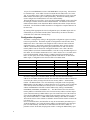
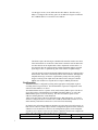
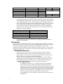
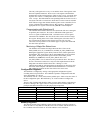
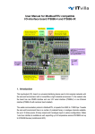
Level 2 Processor Board Technical Reference Manual
Stephen Miller
Zhihui Huang
August, 98
General Description
This document describes the Level 2 Processor (or Alpha) board used to determine the Level 2
trigger decision. It is a 9U VME board that sits in the CDF Level 2 Trigger Crate. The design is
based on the Digital AlphaPC164 motherboard with a 500 MHz Alpha CPU. The board has 4
PCI1 devices added to the PC164 design which provide the interface to the rest of the trigger
system. These interfaces are a VME interface, a Magic Bus to PCI DMA interface, a Magic Bus
to PCI programmed I/O interface, and the interface to the Trigger Supervisor. A block diagram of
the board function is shown in Figure ??
This document assumes that the reader is familiar with the PC164 board design, the Magic Bus
specification, the Tundra Universe chip, the PCI specification and the CDF VIPA crate
specification. Any conflict between this document and those specifications should be assumed to
be an error by somebody.
There is no expressed or implied warranty that the Level 2 board will function as specified or that
it will successfully trigger on signatures for Higgs , SUSY or other exotic particles.
PC164 Based Design
The Level 2 Processor board is based on the Digital PC164 design. The following devices are
based on the PC164 design.
•
The CPU is a 500 MHz Alpha 21164 chip which uses a 50 MHz oscillator.
•
The 21172 chip set has the 21172-CA chip which provides the interface from the CPU to
the PCI bus and the control and addressing for main memory and 4 21172-BA chips which
provide the data path to main memory.
•
There is a 4 MB Level 3 cache.
•
A bank of 8 SIMM slots can provide from 16MB to 512MB of DRAM memory
depending on whether 4 or 8 SIMMs are used. Using 8 SIMMs means that the 256 data path is
used, leading to improved performance.
•
A Xilinx XC17128 SROM contains the boot code that is loaded into the 21164 at power
up. This SROM is installed in a socket. There is also a direct serial interface to a terminal line
connector mounted on the front panel.
•
The PCI bus is the main I/O bus for the board. It is a 64 bit wide bus running at 33 MHz.
There are two 64 bit right angle connector expansion slots for 5V PCI cards.
•
A CMD646 PCI-IDE interface chip supports 2 IDE connectors on the board for hard
disk drives. There is a power connector and mounting holes for 1 hard drive to be directly
mounted to the board. The hard drive should be less than 1 inch thick to stay within the available
space in the crate.
•
A PCI-ISA bridge (Intel 82378ZB ) is connected to an SMC FDC37C935 combination
controller chip which provides support for:
1.
A mouse and keyboard which are connected through 2 mini-din connectors on the front
panel.
2.
A floppy drive which can be mounted directly to the board.
3.
A bi-directional parallel port on the front panel
4.
Two serial D-sub 9 connectors on the front panel
1
5.
A time-of-year clock.
The ISA bus is used to access the 1MB of flash ROM which contains the system firmware. The
ROM is soldered to the board and must be programmed in situ.
•
Two AMD Mach210-15 PLDs are used on the board for PCI interrupt handling and PCI
bus arbitration. These two chips are mounted in PLCC sockets.
VME Interface
Tundra’s Universe II chip is used to provide the VME interface. The Universe chip supports up to
64 bit PCI and VME transfers including DMA transfers. The Universe II databook should be
referred to for the use of the chip. The Universe II chip is connected to all 7 levels of VME
interrupts. Interrupt line LINT(0) of the Universe chip is connected to pin 31of the board’s
interrupt PAL. This PAL register corresponds to bit 2 of ISA address 804. See page 4-15 of the PC
164 TRM for details. The registers internal to the Universe chip must be appropriately set for use
of the interrupts. A front panel reset button will reset the Universe and VME buses.
Description of Operation
This section gives an overview of the operation modes of the Universe chip. The
Universe II user manual should be referenced for a detailed description. The Universe
supports read and write transactions originating from the VME or PCI side. For
transactions originating on the VME side, the Universe acts a VME slave. If the VME
address falls inside the address range defined for one of the 8 VME slave images, the
Universe becomes the PCI bus master and initiates the appropriate transaction on the PCI
bus. To see if the VME slave image is being addressed, the upper 16 bits of the 32 bit
VME address are compared to base and bound addresses for that slave image. This means
the slave image window will be at least 64 Kbytes wide, and can be up to 4Gbytes wide.
(Note that slave images 0 and 5 use the upper 20 bits and thus have 4 Kbyte resolution.)
The corresponding 32 bit PCI address asserted combines the VME address with the
address in the translation offset register. The lower 16 bits of the VME address are used
for the lower 16 bits. The upper 16 bits are derived from a two’s complement addition of
the upper 16 VME bits with the 16 bits of the translation offset register. There are also
control bits for each image which further define the transaction. The transaction can be
coupled in which case the PCI transaction must finish for the Universe to respond to the
VME side; or it is posted for a write, or prefetched for a read in which case an
intermediate FIFO is used and the Universe can acknowledge on the VME side before the
PCI transaction occurs. The Universe acts in much the same way if the transaction
originates on the PCI side. Again there are 8 PCI target images whose registers define
address windows and translation offsets. These images also have 64 Kbyte resolution
with the exception of images 0 and 4 which have 4 Kbyte resolution. However, the PCI
side does not support prefetched reads. Furthermore, if the PCI window is defined to be
in PCI I/O space, posted writes are not allowed either, and all transactions are coupled.
DMA transfers can be initiated from either side. …
Register Configuration
PCI Configuration Registers for the Universe II are accessed on the Alpha by asserting
IDSEL 16 during a configuration read or write. This is a typical PCI configuration space.
The PCI configuration registers 0x10 (and 0x14 ) define the base address for the
Universe’s 4Kbyte register space.
The Universe’s 4Kbyte register space has 3 logical sections. The lowest 256 bytes of the
register map to the PCI configuration space. The upper ?? bytes map to the VME
2
Configuration and Status Registers. The middle part of the space is the Universe Device
Specific Registers (UDSR). [0x10 and 0x14 both point to the same set of registers, but
one does it in memory space and one in I/O space. Which is which depends on a powerup configuration.]
The Universe Device Specific Registers(UDSR) are used for configuring the PCI target
and VME slave images, DMA transfers, interrupts and most other functionality of the
Universe II chip. To configure a PCI target image, one must write to 4 (32 bit) registers.
These registers set control bits, the base address of the image, the bounding address of the
image and the translation offset image. For example
Magic Bus DMA Interface
The Magic Bus (MBUS) DMA interface provides a direct path for MBUS data to be placed into
main memory. The PCI device is actually implemented in two separate programmable chips. A
Xilinx XC4006E-2PQ160c is a (32 bit) PCI target (slave) which is accessed to write to the MBUS
to PCI address translation buffers. These buffers are a set of four 2Kx8bit static RAM chips. A
Cypress CY7C372-125JC CPLD is used as the PCI master to write the data from the input FIFO
to main memory.
Description of DMA Operation
The Level 2 Interface boards send their data to the Alpha boards over the Magic Bus by
addressing one of the DMA channels in the 32 bit Magic Bus Address space. The DMA
addresses are reserved to be the lowest 256 addresses in MBUS address space. These
correspond to MBUS Address bits 31:8 being set to zero.
Each interface board will be assigned its DMA channel(s) to use during initialization.
When any of the 256 DMA addresses are asserted on the MBUS, the Alpha board will
clock the 128 bits of MBUS data and lowest 8 bits of the MBUS address into a 1K deep
FIFO. The Alpha board will also respond with DDONE*, ending that MBUS transaction.
The Alpha can keep receiving data into the FIFO independent of any action on the part
of the rest of the DMA engine. If the FIFO fills up, no error is given, and subsequent
data sent to the Alpha will be lost, although in practice this should never be a problem.
As soon as the FIFO is not empty, the CPLD will start sending data to main memory.
The CPLD initially arbitrates to gain control of the PCI bus and starts sending data as
soon as it can. The 8 bits of the DMA channel are used to address the 4 SRAM chips of
the Translation Buffer (TB). The Translation Buffer asserts the corresponding 32 bit PCI
address on the PCI bus. On the next PCI clock, the lower 64 MBUS data bits are asserted
on the PCI bus, with the upper 64 bits sent on the following PCI clock. The DMA engine
always performs a 64 bit data transfer, and always sends at least two consecutive data
words following one address.
While sending the data, the address for the next data in the FIFO is compared with the
previous address. If the address is the same, the data is sent as part of the same PCI burst
transaction corresponding to the initial address that was sent.
The 21172-CA chip (which manages PCI access to main memory and the CPU) has a
buffer that holds 8 64 bit words. When the buffer fills up, the 21172 asserts a STOP
signal on the PCI bus. The DMA engine responds to the signal by ending the transaction,
releasing the PCI bus and then getting the PCI bus back to finish the transaction. [Note:
The buffer is only used for PCI bursts, that is the buffer is cleared before accepting data
for another address. Also, the buffer is aligned on a 512 bit boundary, so will fill up
sooner if address is not on a naturally aligned 512 bit boundary.]
While the data is being sent, the PCI address in the Translation Buffer is incremented to
point to the next PCI address for that DMA channel. The PCI address is incremented by
3
16 bytes for each MBWORD sent since each MBWORD is 16 bytes long. It should also
be noted that only a 16 bit Adder is used to increment the PCI address bits (18:3) in the
TB. As a result the upper 13 bits are unchanged. That means that for a given event, each
DMA channel cannot write past a 512K byte boundary. Therefore the starting address
used to configure the TB should not be too close to that boundary.
When all the data is received for a given event, the Translation Buffer can be read to find
the ending PCI address written into the Translation Buffer. The difference between the
initial and final address in the Translation Buffer indicates the number of bytes that were
transferred. The Translation Buffer must then be reconfigured to setup the addresses for
the next event.
By turning off the appropriate bit in PCI configuration space, the DMA engine will not
automatically try to send data from the FIFO to main memory. In that case the FIFO
would still receive data and eventually fill up.
Configuration of system
The FPGA is configured by writing to the appropriate configuration registers according
to the PCI specification. The FPGA responds to configuration reads and writes when
IDSEL 20 is driven. The CPLD is not configured. Table xx lists the values of the PCI
configuration space. ( The FPGA is not fully PCI compliant, and so its base memory
address is not automatically configured by the system software. In that case the base
memory address must be written into configuration address 0x10. That is the base
memory address used for the Translation Buffer.) In order to set up the DMA engine as a
PCI master, bit 2 for address 0x04 must be set to 1. Bit 1 must be set to 1 to enable writes
to the Translation Buffer. Simply writing 7 to address 0x04 will accomplish both of
those. At start up the device will be configured with the enable bits set. To turn off the
DMA engine, a configuration write can turn off bit 2 for address 0x04.
31
0x0CDF
0000 0100 0000 0000
0x0601
0xXXXX
0x0000
0x0000
16 15
0
0x0DEA
0000 0000 1000 0XXX
0x3748
0x0000
0x01XX
0x0000
Address (hex)
00h
04h
08h
10h
3Ch ??
All others 14h-38h
Description
Device ID
Vendor ID
Status
Command
Class Code
Revision ID
Base Address Register
Interrupt
Undefined Addresses
In order to configure the Translation Buffer, the CPU must write the main memory
address for each DMA channel into the TB. The TB buffer holds 256 addresses which are
accessed by the CPU by writing to the FPGA base memory address + 4(times)DMA
number. The DMA number is 0 to 255 and directly corresponds to the corresponding
MBUS address. The PCI address is 4 times that since we are accessing 32 bits of data and
a PCI memory transaction addresses at the byte level. For example, for base memory
address 0x02000000 the TB buffers would be addressed by writing to 0x02000000,
0x02000004, 0x02000008, 0x0200000C etc… The data written to the TB is the main
memory address to which data will be sent. The main memory address used must map to
a part of the main memory’s DMA address space. The location and size of the window is
set by the FLASHROM firmware by writing to the appropriate register in the 21172-CA
chip. For the EB164 there is a 1 MB DMA window starting at PCI address 0x100000.
The location and size of the window are defined in the eb164.h file and the executed code
is
in eb164_io.c.
Note:
As mentioned above, the TB buffer can only be incremented by the Adder up to a
512K byte boundary. As a result, the memory address used should not be near the upper
part of a 512K boundary. It should also be noted that since the cache is 4MB, it is
preferable to have all the data (and program) stored in a contiguous 4MB memory space.
4
Magic Bus Programmed I/O
The Magic Bus Programmed I/O chip (MAGICFPGA) is a bridge between the PCI and Magic
Buses which allows reads or writes from one address space to the other. The PCI-MBUS
transaction can originate from either side and can be either a read or a write. This allows the CPU
to directly access the Magic Bus memory space or for a board on the Magic Bus to write or read
into PCI memory space. The FPGA supports up to 64 bit PCI data transfers but only 32 bit
addressing, and accesses all 128 bits of MBUS data. This device is implemented in a Xilinx
XC4036EX-2-PG411C.
Description of Operation
PCI Transactions
Addressing in PCI memory address space is accomplished by using the lines
AD(31:2) to address a DWORD (4 bytes). The MAGICFPGA must convert this
addressing scheme to the MBUS address, where the MBUS address lines (31:0)
address a single 128 bit MBWORD (16 bytes). When the CPU initiates a read
or write to the MBUS, it can choose one of two PCI address windows to address
the MAGICFPGA. These are called Window A and Window B. Each of them is
a 64K space in PCI memory address space and their base PCI address is set in
the PCI configuration register as described below. Both windows still access the
same MBUS address space which is fixed by the PCI Translation Base. The
purpose of having separate windows is described in detail later on.
The upper 16 bits of the PCI Translation Base gives the upper 16 bits for
converting a PCI address to a MBUS address. Since 16 bits are used for the
translation, that means only 64K of contiguous MBUS address space can be
addressed. In order to address a MBUS address that is not within 64K of the PCI
Translation Base address, the PCI Translation Base register would have to be
updated before attempting to read/write to that MBUS address. Figure xx
illustrates how a PCI address is converted to a MBUS address.
When the PCI side initiates a read or a write to the MBUS, the FPGA will try to
gain control of the MBUS and then perform the transaction. The PCI and MBUS
transactions are coupled so that the PCI transaction doesn’t end until the MBUS
transaction is finished. If the FPGA cannot gain control of the MBUS within 16
5
PCI cycles, it will assert STOP on the PCI bus. This will signal the 21172 to
retry the transaction, so no software retry will be necessary. If the FPGA is
simultaneously addressed from both the MBUS and PCI sides, the transaction
originating on the MBUS will take precedence and the PCI transaction will fail.
[Note: If the FPGA gains control of the MBUS, but then the MBUS transaction
hangs, that will hang the PCI bus indefinitely.]
The two PCI windows on the MAGICFPGA are accessed separately by two
different PCI addresses. However, their purpose is not to address separate
MBUS addresses but to allow for two different types of PCI transactions. PCI
transactions can occur as 32 bit or 64 bit, can be burst or non-burst, and can be
from sparse or dense memory space. Having the two windows allows some
flexibility in having different types of transactions.
The basic difference in the two windows is that Window A is used for PCI data
transactions of less than 128 bits, while Window B always requires a PCI
transfer of 128 bits. In either case, the Magic Bus transaction is a full 128 bits,
but the data read or written may not all be meaningful for Window A. The
distinction between Window A and Window B is related to the distinction
between PCI sparse memory space and PCI dense memory space.
When writing to Window A, the MBUS transaction starts when the last PCI data
transfer occurs. (The last data transfer is indicated by the PCI protocol.) The
data can be just 32 bits or up to 128 bits in a burst transaction, although the burst
should not go past 128 bits. Window A should be mapped in the PC164’s PCI
sparse memory space which is defined to be in the physical address range
80.0000.0000 to 85.7FFF.FFFF. See the PC 164 TRM for details of the address
space.
Window B only initiates a MBUS transaction after a 128 bit transfer has
occurred, which can be done via a burst of 4 32 bit transfers or a burst of 2 64 bit
transfers. Window B should be mapped to the dense memory space which is
defined to be in the physical address range 86.0000.0000 to 86.FFFF.FFFF. The
software accessing Window B must always perform a 128 bit transaction, in
order for the MBUS transaction to occur. The addresses must also be aligned on
a 128 bit boundary.
A read into either Window A or Window B will trigger a 128 bit read on the
Magic Bus. The FPGA can support a burst read of up to 128 bits using either 32
or 64 bit transfers. The FPGA returns the lowest 32(64) bits on the initial read
and continues to send the upper bits if it is a burst transaction.
Magic Bus Transactions
A transaction originates on the MBUS side when an address asserted on the
MBUS falls between the MBUS Upper Memory Address and the MBUS Lower
Memory Address. These addresses must be configured in a register on the
FPGA as described below. This causes the FPGA to ask for control of the PCI
bus and it will remain in that state until control is given. After receiving control,
it initiates a 64 bit PCI transaction and will perform two 64 bit reads/writes in a
PCI burst transaction. The FPGA will not end the MBUS transaction with the
DDONE* signal until the PCI transaction is finished.
The MBUS Upper Memory Address and MBUS Lower Memory Address define
the window in MBUS address space for which the Alpha board will respond to a
posted MBUS address. Only the upper 16 bits are used for the comparison so
the smallest window defined is 64K. The MBUS Translation Base defines the
base PCI address used for converting a MBUS address to a PCI address. In this
6
case the upper 12 bits (31:20) define the base PCI address. Therefore only 1
Mbyte of contiguous PCI memory space can be addressed. Figure xx illustrates
how a MBUS address is converted to a PCI address.
The FPGA requires the PCI target to handle 64 bit transfers and does not check
if the 64 bit transfer is not allowed. That means it cannot be used to address the
two other FPGAs on the Alpha board as those only handle 32 bit transfers. It
also currently does not respond to the PCI STOP signal that might be returned
by the target. This is a potential bug and will be fixed in an updated design.
Currently the state machines that handle MBUS transactions are synchronized to
the PCI clock. This means a 30ns delay between state transitions. Although this
simplifies the design, it results in a performance penalty. Once the prototype
design is working on the Alpha board, the FPGA will be changed so that the
MBUS state machines are asynchronous to improve MBUS performance.
Configuration
The MAGICFPGA is configured by writing to the appropriate configuration registers
according to the PCI specification. The MAGICFPGA responds to configuration reads
and writes when IDSEL 21 is driven.
The MAGICFPGA asks for 3 separate 16 bit (64 K) memory address spaces. The first is
for on chip registers which hold the PCI to MBUS translation address, as well as the
MBUS address space reserved for the chip. The other two address spaces are PCI
addresses defining Window A and Window B.
Table xx lists the values of the PCI configuration space. Bits indicated by “X” must be
written to configure the device. The last 3 bits of address 04h should be written as 110 to
enable memory reads/writes to the device as well as PCI bus mastership.
In principle, the PCI memory addresses should be set by the plug-n-play PCI protocol. In
that case user software would simply read these configuration registers to know what PCI
addresses to use for that device. However, the configuration registers can be changed at
any time by user software. In that case the software should be careful to not configure the
device with a PCI address used by another device on the board.
31
16 15
0 Address (hex)
Description
0x2CDF
0x2DEA
00h
Device ID
Vendor ID
7
0000 0100 0000 0000
0x0701
0xXXXX
0xXXXX (Window A)
0xXXXX (Window B)
0x0000
0x0000
0000 0000 1000 0XXX
0x3748
0x0000
0x0000
0x0000
0x01XX
0x0000
04h
08h
10h
14h
18h
3Ch
All others
Status
Command
Class Code
Revision ID
Base Address Registers
Interrupt
Undefined Addresses
The base memory address at configuration address 10h defines the base memory address
for the Magic Bus configuration or “setup” space. These “configuration” registers are not
in PCI configuration space, but are accessed through a normal PCI memory transaction.
These registers hold the mapping from PCI to MBUS address space and vice versa. Table
xx describes the memory location of each of the registers. The address is the address
given in the table, plus the base memory address as defined in the PCI configuration
register 10h. These registers must be configured by user code for proper function of the
MAGICFPGA with the Magic Bus.
Register Description
PCI Translation Base
MBUS Upper Memory Address
MBUS Lower Memory Address
MBUS Translation Base
MBUS Mask (not used)
Address (hex)
00h
04h
08h
0Ch
10h
PCI configuration registers 14h and 18h must be configured with the PCI address for
Window A and Window B.
TSI Interface
The TSI interface is implemented in a Xilinx XC4010e-2PQ208c FPGA (TSIFPGA). This chip
only functions as a PCI slave and is used to receive and send information to the rest of the trigger
system. This includes the CDF trigger signals from the P2 backplane, as well as direct
communication with the Global Level 2 board through a front panel connector. It is also used for
monitoring the status lines of the Magic Bus. Some of the described features of the TSIFPGA are
specific to the CDF version.
Description of Operation
Because the device is a PCI slave, the only PCI operations are reads and writes to
registers within the FPGA. Once the device has been configured with its base PCI
memory address, one reads or writes to specific registers using the base address+local
address. This device only supports 32 bit PCI transactions.
The device has one of its pins connected to the PCI interrupt PAL at pin 9. With the
interrupt PAL code, this corresponds to bit 2 of ISA address 805. See page 4-15 of the
PC164 Technical Reference Manual for details. Currently the FPGA interrupt pin is
simply pulled high, although it could easily be controlled by a register bit.
CDF Trigger Signals
The TSIGPGA is connected to 37 CDF trigger signals on the P2 backplane.
One of these is the CDF_CLK signal which gives the time when the other
signals are valid. The CDF clock signal is actually a differential PECL signal on
the backplane and is converted on board to a single TTL level clock signal. This
signal is used to clock the registers whose inputs are the signals directly from the
backplane. Another CDF signal is CDF_ERROR* which is an output from the
FPGA. This output drives an open collector driver connected to the
corresponding P2 line. All of the other 35 signals are directly connected to the
P2 backplane.
8
The CDF_CLK signal arrives every 132 ns and the values of the registers in the
FPGA are updated at that time. There are two 32 bit registers which hold the
updated values of the CDF trigger lines. There are also a set of “processed” data
registers. One of these is a 4 deep FIFO which is written to whenever there is a
Level 1 accept. This FIFO holds the corresponding buffer bits for that L1A. It is
read by the CPU after a L2 decision to know that a L1A has occurred, and what
buffer will have trigger data loaded. Similar registers can be constructed for L2
accepts, Calibration bits and Halt, Recover, Run sequences. Writing to the
appropriate bit in a register will assert CDF_ERROR* on the backplane.
Communication with Global Level 2
The communication with the Global Level 2 board in the TSI crate is through a
68 pin front panel connector. We send 16 differential LVDS signals and
receive 16 signals of differential LVDS. On board we have 32 TTL signals
connected to the TSIFPGA. The value of all 32 bits can be read from a single
PCI register. Writing to the lower 16 bits of that register will set the values of
the 16 output signals which are then directly sent to the TTL to LVDS
converters. It is not possible to write into the upper 16 register bits which hold
the value of the input lines.
Monitoring of Magic Bus Status Lines
The TSIFPGA also monitors the Magic Bus status lines. These are the
MOD_DONE(18:0), EV_LOADED(4:0), and MB_AP_FIFO_EMPTY lines.
Reading the appropriate register directly reads the value of these signals from
the backplane. The empty status of the on board DMA FIFO is also read from
this register. Writing to another register will drive the START_LOAD,
BUFFER(1:0), MBRESET, and AP_FIFO_EMPTY lines. This
AP_FIFO_EMPTY line is connected to an open collector driver. The other 4
lines are connected to a transceiver. Only one of the Alpha boards will be the
Magic Bus crate master and drive these lines. Writing a 1 to the
CRATE_MAS_DIR bit will appropriately set the transceiver direction to drive
these lines on the backplane. The other boards should then have a 0 written to
that register bit, in which case the value of these lines can be read.
Configuration Registers
The TSIFPGA is configured by writing to the appropriate configuration registers
according to the PCI specification. The TSIFPGA responds to configuration reads and
writes when IDSEL 23 is driven.
The TSIFPGA asks for a 16 bit (64 K) memory address space. Table xx lists the values of
the PCI configuration space. Bits indicated by “X” must be written to configure the
device.
The last 3 bits of address 04h should be written as 010 to enable memory reads/writes to
the device. Writing to the upper 16 bits of 10h specifies the base memory address. In
principle, that address should be set by the plug-n-play PCI protocol.
31
16 15
0 Address (hex)
Description
0x2CDF
0x2DEA
00h
Device ID
Vendor ID
0000 0100 0000 0000
0000 0000 1000 0XXX
04h
Status
Command
0x0701
0x3748
08h
Class Code
Revision ID
0xXXXX
0x0000
10h
Base Address Register
0x0000
0x01XX
3Ch
Interrupt
0x0000
0x0000
All others 14h-38h Undefined Addresses
Memory Registers
The memory location of the TSIFPGA registers and the signals accessed by each bit are
shown in Table xx. Only addresses 00h, the lower 8 bits of address 10h and the lower 16
bits of address 14h can be written to. All of the addresses can be read from.
9
Adress
00h
04h
08H
0Ch
10h
14h
Currently the “processed” CDF data registers are not implemented.
Bits
Description
31:0
Generic read/write register
CDF Trigger Signals
0
L1A*
1
L1R*
2
L2B0*
3
L2B1*
4
GLIVE*
5
L1W1*
6
L1W2*
7
L2DB0*
8
L2DB1*
9
L2A_EN*
13:10
EVID(3:0)
14
L2A*
15
L2R*
16
STOP*
17
HALT*
18
RECOVER*
19
TEST*
20
RUN*
21:23
RL(2:0)
24
BC*
25
B0*
26
ABORT*
CDF Trigger Signals
0
CALEN*
1:7
CALIB(6:0)
15:8
0x01 (constant)
23:16
0x01 (constant)
31:24
0x01 (constant)
18:0
MOD_DONE(18:0)
19
FIFO_EF*
20
MB_AP_FIFO_EMPTY
24:21
EV_LOADED(3:0)
31:25
0x01 (constant)
0
CDF_ERROR*
1
AP_FIFO_EMPTY
2
CRATE_MAS_DIR
3
(undefined)
4
BUFFER(1)
5
BUFFER(0)
6
START_LOAD
7
MBRESET
31:8
(constant)
15:0
TSI_OUT(15:0)
31:16
TSI_IN(31:15)
PCI Interrupts
There are also 4 interrupt lines from each of the PCI expansion connectors connected to the
interrupt PAL, as well as interrupts from the SIO and IDE drivers. The Universe interrupt is
10
masked/read at ISA address 804- bit 2. The TSIFGPA interrupt is masked/read at ISA address
805-bit 2. The other interrupts are as described in section 4.5 of the PC164 TRM.
PCI interrupts are handled by the board's Interrupt PAL chip which has all of the PCI device's
interrupts going to it. This PAL then sends out one general PCI interrupt to the CPU. To find out
which device caused the interrupt, one has to read a register on the PAL chip, which is located in
ISA address space. There is one interrupt line from the Universe chip and one from TSIFPGA that
are connected to the interrupt PAL.
Resets
PCI Devices
We list each of the PCI devices, their IDSEL line, and the 21164 physical address for their
configuration space. Compare this to Table B-9 on page B-14 in the PC 164 TRM. I presume the
Physical Address will have to be set in the Firmware.
PCI Device
IDSEL line
Physical Address
Universe
16
87.0005.0000
PCI slot 0
17
87.0006.0000
PCI slot 1
18
87.0007.0000
SIO (ISA) bridge
19
87.0008.0000
DMA FPGA
20
87.0009.0000
Magic FPGA
21
87.000A.0000
IDE controller (Hard Drive)
22
87.000B.0000
TSI FPGA
23
87.000C.0000
Power Requirements
We estimate the Alpha board requires the following voltages and currents from the crate power
supply:
•
+5 V 20 A from J1 and J2
•
+3.3 V 10 A from J1
•
+12 V 2 A from J1
•
-12 V
1 A from J1
•
-5.2 V 1 A from J2 (Vw pins)
2.5 V for the Alpha chip is generated on board using 5 V for the power source.
Jumper Configuration
The jumpers on the Alpha board are the same as those on the PC164 board design. This section
describes how the jumpers should be set. The PC164 TRM can be referenced for further details.
•
J1 is IN when using 4 SIMMs for a 128 bit data bus and is OUT when using 8 SIMMs
and the 256 bit data bus.
•
J31 is used to enable/disable the Flash ROM being updated. Pins 2 and 3 should be
connected to enable writing or pins 1 and 2 should be connected to disable writing.
•
J30 is used to configure various cpu related quantities that are read at boot time. IRQ0-3
defines the ratio of the CPU clock frequency to the system (PCI) frequency. (I’m not sure where
this is read or used in the srom code, but 500/15 = 33.3) CF0-7 can be HARD_WIRED in the srom
code which is likely what will be done for some of the parameters. Cache size is currently set to be
configured as 2Mbytes which is less than the 4Mbytes of actual cache. Similarly the cache speed
is set at 9ns, whereas the actual chips are 7.5ns. These numbers will need to be changed in the
srom code.
Jumper pins Name
Purpose
Default
1-2
IRQ3
System clock freq.
Out
3-4
IRQ2
System clock freq.
Out
5-6
IRQ1
System clock freq.
Out
7-8
IRQ0
System clock freq.
Out
9-10
CF0
Reserved
11-12
CF1
Cache size
Out
13-14
CF2
Cache size
In
11
15-16
17-18
19-20
21-22
23-24
25-26
12
CF3
CF4
CF5
CF6
CF7
Reserved
Cache speed
Cache speed
Mini-debugger
Boot option
Not Used
Out
Out
Out
Out