1
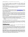
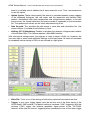
APV6 Vienna Manual
How to handle DAQ and analysis hard- and software
M. Friedl, HEPHY Vienna
Email: [email protected]
V0.91 Feb 19, 1999
APV6 Vienna Manual – How to handle DAQ and analysis hard- and software
2
Document Source & Related Documents
This document is electronically available at
http://wwwhephy.oeaw.ac.at/u3w/f/friedl/www/apv6/
where it can be downloaded in PDF and PS formats. In the same place, our
transparencies from talks at the CMS meetings and a more general APV6 info paper can
be found.
Definitely the most important source of knowledge concerning the APV6 chip itself is the
Reference Manual, which can be found at
ftp://ftp.te.rl.ac.uk/apv6/user_manual/apv6_user_manual_2.0.ps
(The blanks are in fact underscore characters.) Basic knowledge about the APV6, which
can be obtained by the manual mentioned, is required for understanding this paper.
Introduction
This paper describes the hard- and software that is currently available and operable at the
HEPHY Vienna. Many items may be of principal interest concerning the APV6, others are
device-specific.
The intention of the Vienna hardware was not to work towards a final CMS readout
design, but rather to have a compact stand-alone system, which is easily transported to
test beams or operated in the lab. Thus, the hardware is limited to the readout of 4 APV6
chips, 3 of which are currently attached.
Certain items of the readout system may be altered in future, in that case the logbook
and/or module schematics should be concerned.
Hardware
General block diagram
The following block diagram contains all hardware blocks that can be connected to the
system. However, some devices are not obligatory: The Mac488B Bus Controller (serial to
IEEE 488 interface) is only necessary when detector voltage/current monitoring by the
DAQ is desired. The VME CTR module, which controls delay and attenuation modules in
the NIM crate is only required for special pulse scans over time. Also, one can do without
the temperature monitoring.
APV6 Vienna Manual – How to handle DAQ and analysis hard- and software
3
Vienna APV6 Readout System
Detector/Hybrid/Repeater
Mac488B
Keithley 237 SMU
Silicon
Strip Detector
3 APV6s
on Hybrid
Repeater
Electronics
Voltage
Regulators
Cal Pulse
Generator
12 different geometry
zones, 32 strips each
384 strips in total
Temperature Sensors
Scintillator/
Photomultipliers
NIM Crate
VME Crate
HV Supply and
Discr./Coinc.
Logic
or
Trigger and
Delay Logic
Random
Clock
Crate
Controller
Delay
CTR
VME
↔
IC
Clock
APV6 Read 2
2
Optional Components
ADC
Board
VME
Interface
DAQ
Software
Harddisk
Data
Storage
PC
Serial
Interface
In the subsequent sections, all the hardware devices are described in detail.
Detector/Hybrid/Repeater
These components, mounted together on a plastic support, are the very heart of the
system. The support fits into a green cooling box (12V ≤10A), which must be flooded with
inert gas (N or He) when operating to avoid condensation of water on the electronic parts.
A few months after the testbeam, the cooling box was operating for approximately one
APV6 Vienna Manual – How to handle DAQ and analysis hard- and software
4
week without gas flooding for a scan of the bias settings. After that, the floor of the box
was entirely covered with water and the electronics was really wet… Also the detector has
taken some damage at this unfortunate event, some strips now show up with excess
noise.
CAUTION! Care must be taken when handling the support, as the detector's backplane is
uncovered at the bottom and the aluminum window on top is very fragile.
Repeater
APV6 Hybrid
Detector
Temperature
Sensors
Connectors
Detector
CAUTION! Extreme care must be
taken with both detector and APV6
when handling or soldering nearby.
Never touch these components with
bare fingers! The wire-bonds are
extremely fragile!
The detector currently installed is a
2
6.25 x 6.25 cm multi-region sillicon
detector (#12) manufactured by the
Hamamatsu corporation. It consists
of 12 zones with different strip
geometries. Each zone has 32
strips, making 384 strips altogether,
matching the number of inputs of 3
APV6 chips (128 input channels each).
The detector zones have different strip pitches and implant widths. Viewed from the side
with the APV6 chips, the zones and strips are numbered from left to right.
Zone number
0
1
2
3
4
5
6
7
8
9
10
11
APV6 Vienna Manual – How to handle DAQ and analysis hard- and software
5
Strip pitch
[mm]
60
80
240
120
60
80
240
120
60
80
240
120
Implant width
[mm]
25
40
70
50
20
25
50
35
15
15
30
20
Strip numbers
0..31
32..63
64..95
96..127
Zone
limits
[mm]
0
3.14
6.92
128.159 160..191 192..223 224..255 256..287 288..319 320..351 352..383
15.78 20.80 23.94 27.72 36.58 41.60 44.74 48.52 57.38 62.40
Note that the various zones are not of equal widths, due to the different pitches. This
causes some complication when, e.g., plotting a beam profile (hits vs. strips): The
(usually) Gaussian shape is not linearly projected onto the strips for two reasons. First, the
various strip pitches cause geometric distortions in the shape and second, the hit
probability (or collection) depends on the area, which again depends on the pitch.
Furthermore, a fraction of hits is lost in the inactive regions between the zones.
On the side opposite to the APV6 chips, the guard ring of each detector zone is connected
to the ground rail. Each strip is equipped with an integrated FOXFET bias resistor between
the strip and the guard ring.
Due to the guard rings, the first and last strips of each zone (strip numbers 0+32z, 31+32z;
z=0,1,2,…,11) have a higher ground capacity than mid-zone strips, causing excess noise.
Thus, only strips 1..30 in each zone can collect hits. Taking the inactive regions into
account, one expects a collection efficiency in the order of 70%. In practice, the fraction
depends on the hit cut parameters, since signal and pedestal are not clearly separated
with a SNR≈12, which is roughly achieved with the APV6.
The strip capacity of the current multi-region detector is between 8 and 12 pF, depending
on the geometry. In the final design of the CMS tracker, two detectors are connected in
series, giving a 6.25 x 12.5 cm2 area. In that case, the detector strip capacity is twice that
of the single detector, causing more noise. The strip pitches in the CMS tracker will be 60,
80, 120 and 240 µm from the inner to the outer layers, giving a tradeoff between spatial
resolution and the number of channels. The current multi-region detector was designed to
examine the various implant widths.
The thickness of the detector is 300 µm, it is based on an n-type bulk (and backplane) with
p-implants for the strips. The cable for the bias voltage ends with a BNC connector, which
must be fed with positive voltage, which leads to a reverse biased pn-junction.
CAUTION! Make sure never to apply even the smallest negative voltage to the detector,
as the diode may easily take damage from forward biasing.
Bias voltage +100 V should be entirely secure. The dark current drawn is normally <1 µA,
thus a compliance of a few microamps should be fine. However, the 240 µm pitch zones
may not yet be completey depleted, for them, +150 V is better. However, the detector may
show some kind of breakthrough at this voltage, after which it must rest for at least several
hours. Thus, be careful when applying the bias voltage.
When minimum ionizing particles (MIP) traverse a fully depleted 300 µm silicon detector,
the resulting charge spectrum, after pedestal contamination is removed, has a most
probable (MP, =maximum) value of 22400 e and a mean value of around 31000 e. The
spectrum can be approximated by a Landau distribution.
APV6 Vienna Manual – How to handle DAQ and analysis hard- and software
6
The final detector, however, should withstand at least 500 V. With increasing radiation
damage, the depletion voltage decreases in the beginning until the point of type inversion,
then it increases continuously . At the end of the scheduled 10 years of LHC operation, a
voltage in the order of 500 V will be applied in order to achieve depletion.
There are 2 glass fanouts between the detector strips and the APV6 inputs. Their task is
not only to match the different geometries, but also to allow non-destroying separation of
hybrid and detector. Both the detector and the chip bond pads are very small and do not
allow more than 1 bond. When such an existing bond is removed, there is very low
probability than another bond will stick there. On the glass fanouts, however, there is
ample space for many bonds.
Consult M. Krammer for further information concerning the detector.
Hybrid
CAUTION! Extreme care must be taken with
both detector and APV6 when handling or
soldering nearby. Never touch these
components with bare fingers! The wirebonds are extremely fragile! Soldering
requires a ground connection to the iron tip!
The hybrid was manufactured by the
Imperial College (IC, London, UK). It can
support up to 8 APV6 chips, but in our setup
only holds 3 of them.
The APV6 chip, designed by the Rutherford
Appleton Laboratory (RAL, Chilton, UK),
consists of 128 identical channels with
preamplifier/shaper stages, a 160 cell
analog pipeline and a deconvolution network
each. Surrounding elements are the digital
2
logic including an I C bus, the bias generator
and the output multiplexer.
For details concerning the APV6 chip,
please consult the APV6 user's manual (see
p. 2).
The general function flow of the APV6
operation is the initialization over the I2C
bus, after which a reset must be given. (Each chip has unique I2C addresses for writing
and reading.) Then, the chip is ready and waiting for triggers. According to the pipeline
architecture, the triggers may appear up to 160 x 25 ns=4 µs after the corresponding
event. This (complicated) feature becomes a necessity in the LHC design, as the trigger
decision is not possible within two bx, moreover, not even signals from opposite ends of
the CMS detector come together within this time. After receiving a trigger, the APV6 puts
out an element of the pipeline, which is a certain number of bx (or clock cycles) in the
past. This value is called latency (LAT) and is configured during initialization.
The shaper ouput is sampled and stored in the pipeline ring buffer with every clock cycle.
In the peak mode, these values are sent to the output directly, while in the deconvolution
mode, 3 subsequent pipeline values are mixed together in a switched capacitor filter
APV6 Vienna Manual – How to handle DAQ and analysis hard- and software
7
network (ASPS), resulting in a narrower signal shape, which allows the separation of
signals from subsequent bx.
signal [ADC]
The signal output shape
APV6 calibration pulse shapes
cannot be monitored directly,
peak and deconvolution modes (default bias settings)
as it is sampled when
300
entering
the
pipeline.
250
However, scanning curves
can be recorded either using
200
the internal calibration delay
150
-Peak
(see APV6 user manual) or
100
Decon
by sequentially shifting the
50
external calibration delay.
0
The output shape depends
-50
on the seven bias parameters
-100
and, of course, the mode.
-25
0
25
50
75
100
125
150
Note that the output polarities
t [ns]
differ
in
peak
and
deconvolution modes. In our
setup, deconvolution mode signals are positive, while peak mode signals are negative.
When there is no trigger to the APV6, it sends "alive ticks" every 1.75 µs. A few µs after a
trigger input, a 4 bit header, an 8 bit pipeline address and then 128 analog channel values
are serially pushed out on the output line. The channel values do not appear in the natural
strip order, but they are sent over a multiplexer stage and come in a mixed-up order:
Natural channel order
0
1
3
4
5
15
16
…
Position in output data
0
32 64 96
8
40 72 104 16 48 80 112 24 56 88 120
1
…
2
6
7
8
9
10
11
12 13 14
When two or more triggers
appear within a few bx, the
corresponding pipeline cells
are marked against being
overwritten and a number of
header/address/signal blocks
are subsequently pushed out
after the initial delay of a few
µs. In peak mode, up to 18
such events may occur
before the data is pushed out
without loss of data. In
deconvolution mode, where 3
cells are must be saved per
sample, only up to 6 events
are possible. This leads to
little
signal
loss
with
high
trigger
rates
(see
and
http://pcvlsi5.cern.ch/cmstcontrol/documents/APV_pipeline_inneficiencies.pdf
http://www.hep.ph.ic.ac.uk/leb97/APV6java.html). The 3 cell-mixing in deconvolution mode
APV6 Vienna Manual – How to handle DAQ and analysis hard- and software
8
also implies that the latency time for equivalent timing must be set 3 counts larger than in
peak mode (looking farther back in the past).
In our setup, the three chips are numbered with channels 0..127, 128..255 and 256..383
from left to right (corresponding to the detector strips) when looking at the hybrid facing
the repeater. All channels of the 3 APV6 chips are connected to a detector strip except for
channels 0..2 on the first chip. While 0 and 1 are left open, channel 2 is used for
calibration. It is bonded to an 8.2 pF capacitor with a voltage divider, to which a small
voltage step is applied when calibration is enabled.
Point to measure ∆ V
MAX435
470Ω
(gain)
APV6
4.22kΩ
56Ω
39Ω
8.2pF
current source
output
channel 2
11Ω
680Ω
CLC114
(The output of APV6 #0 is
terminated with 308Ω
-- WHY???)
The capacitor should have a value similar to the detector capacitance. Using Q=CV, one
can derive really small voltage steps needed for charge inputs in the order of 1
MIP=22400 e. To achieve this, an extended voltage divider lies in front of the capacitor.
Experience has shown that a voltage division ratio of, say, 1:1000, cannot simply be
realized by a 2-resistor network, because the stray capacitance between input and output
of the divider (=the top resistor), although only a fraction of pF, together with the 1000
times higher voltage step, feeds much more charge into the amplifier than the real
capacitor. Furthermore, the final division stage should be terminated and as close as
possible to the amplifier input. Considering all these items, the realized network seems to
be a good choice. The actual layout of the calibration pulse injection circuit is really critical
in terms of noise. The final divider stage and the capacitor are therefore SMD components
placed closely together.
In order to calculate the injected charge Q=CV, one has to measure the voltage step for
the Q=CV relation. The nominal capacitance value is 8.2 pF. While the real actual value of
such capacitors usually is somewhat higher, stray capacitance against ground decreases
the value, thus the nominal value seems to be a good deal. It is impossible to measure the
voltage step, which is in the order of 1 mV, directly at the capacitor terminal. However, it
may be possible to probe the voltage at the indicated point, selecting 20 MHz bandwith on
the scope. If this is still too low, the MAX435 output must be measured. In any case, the
actual voltage step must be calculated according to the division ratio.
The linear range of the APV6 is limited to ±5 MIPs. Then the calibration capacitance is
increased, the voltage division ratio must also be adapted in order to get the same charge.
Consult M. Pernicka for further details on the APV6 and other electronic parts.
APV6 Vienna Manual – How to handle DAQ and analysis hard- and software
9
Repeater
The repeater is a rather simple circuitry performing a few tasks. It buffers both incoming
and outgoing signals and it provides the voltages for the APV6 (±2V), the digital and
analog buffers (±5V) and the I2C buffer (+3V, -2V). The clock and trigger signals sent to
the APV6 are not only buffered, but also sent back to the APV6 Read 2 VME card. This
feature allows some independence on the timing. In fact, the VME board does not need to
know the exact timing, which is only specified by the LAT register value (coarse) and the
NIM delay (fine).
Note that the repeater, especially the voltage regulators, dissipate a lot of thermal power.
In the current setup, whole repeater is included in the cooling box. However, I would rather
suggest to place them outside of the cooled environment in future designs.
Keithley 237 SMU and Mac488B
The Keithley 237 Source Measure Unit is used to provide the detector bias voltage (s.
Detector). It must be used with a special BNC-TRIAX interface box with the TRIAX cable
connected to the "OUTPUT HI" terminal at the rear of the device.
First set the compliance value. Set the output voltage to 0 and push the "OPERATE"
button. Always remember that only positive voltages are allowed. Choose the 1V digit
with the "SELECT" buttons and ramp up the voltage with the knob, keeping an eye on the
current. If the current remains in the order of or below 1nA, one can be sure that the bias
line is interrupted somewhere. When the final voltage (probably +100V or +150V) is
reached, hit "ENTER" to remove the cursor.
The voltage/current monitoring is optional and can be switched on and off with the DAQ
software. It only works if there is a Mac488B interface present, which is wired both to the
PC with a DB9-Mac8 serial cable and to the Keithley 237 (IEEE Address 16) with an IEEE
488 cable. The parameters for the serial connection are:
Serial Port
COM2:
Baud rate
9600
Data bits
8
Stop bits
2
Parity
None
Handshaking
RTS/CTS
These settings are the defaults of the Mac488B device. Inside the Mac488B case, there
are 3 rows of DIP switches, with which also the serial parameters can be altered.
Moreover, when facing the front panel, DIP switch #2 in the middle row is pressed down in
the top ("CLOSED") position ("MacDriver488 mode") by default. This mode only works
with a special Mac driver which is not available on the PC. Therefore, this switch must be
pushed down in the bottom ("OPEN") position ("System Controller mode") for the
operation within the APV6 environment.
When you doubt about the connection to the Mac488B, connect with any terminal
program (such as Hyperterminal, which comes together with Windows NT) and send
"hello"+CR to the Mac488B, which should answer with its name and version number.
APV6 Vienna Manual – How to handle DAQ and analysis hard- and software
10
Please refer to the Keithley 237 and the IOTech Mac488B manuals for further information.
VME Modules
The slot position of any VME module is irrelevant, except for the Crate Controller, which
must use the leftmost slot (#1).
Each module uses a certain address range, which, in most cases, can be selected using
DIP switches. The T&M Explorer, which is sort of a VME registry for the driver, must know
all valid address ranges. However, it does not matter if a module specified in the T&M
Explorer does not really exist in the crate. Refer to Helmut Steininger for further
information on this topic.
The table below summarizes the address ranges used for the APV6 setup. The VME
Delay (Clock) is used as a NIM clock source only and thus needs no communication.
VME Device
VME Address Range
Crate Controller (VME-MXI-2)
0x000000 - 0x00FFFF
APV6 Read 2
0xB02000 - 0xB02FFF
2
VME ↔ I C
0xAC2000 - 0xAC2FFF
0xAC3000 - 0xAC3FFF
Delay CTR
0xA10000 - 0xA10FFF
After turning on PC and VME crate, the Resource Manager (ResMan) must be started in
order to initialize the communication. On our current PC, it always hangs up after
everything is done – nevertheless, everything works fine.
Crate Controller
The VME Crate Controller is manufactured by National Instruments and connects to a PCI
card inside the PC via the MXI bus (two thick cables). It is specified for a 32 bit trasfer rate
of at least 10 MB/s, provided that the VME module(s) can push the data that fast. In fact,
our APV6 Read 2 module cannot push out data at this speed. (Nevertheless, it is quite
fast.)
The only interactive element on the front panel is a reset button. Note that after hitting this
button, the Resource Manager (ResMan) must be re-run on the PC to re-initialize the
driver.
VME Delay (Clock)
From this module, only the 80 MHz NIM-Clk output is used. The board also provides a
VME-controlled digital delay, however, this should not be used for precision
measurements.
APV6 Read 2
APV6 Vienna Manual – How to handle DAQ and analysis hard- and software
This is the center of data acquisition. The module
provides the control signals and clock for the APV6,
buffers and digitizes incoming data at 40 MHz and stores
up to 4k words in a FIFO memory.
CAUTION! Approximately since January 1999, this
module intially produces corrupt data when the crate is
switched on, the driver loaded and the DAQ is started.
The only solution found so far is to simply pull out the
card and replug it while the crate remains turned on, but
the DAQ is not running. After that, everything works fine.
In any case, the module must be fed with a (usually
80Mhz) clock, which is divided internally to 40MHz and
sent to the APV6. Furthermore, the connection to the
repeater with a special cable (orange "DELPHI" cable),
which is 21m long, is essential. Do not use other cables,
since the termination resistors of the signal lines are
matched with the cable's impedance (Z=103.5Ω).
Whenever the length of this cable is amended, the timing
values specified in this paper must be adapted. (The
propagation time of 1m of cable is approximately 5ns.)
The module has a veto switch, which is usually turned on.
This feature ensures that an incoming trigger sets a veto
for further triggers until it is reset by the software (after
reading out the data). However, with DIP switches on the
board, the number of subsequent triggers allowed before
vetoing can be selected to be 1..15.
11
Veto LED (out of order)
NIM IN
Clock 80 MHz
NIM IN
TRIG
NIM IN
CAL+TRI
NIM IN
CAL+TRI_Syn
NIM IN
CAL In
NIM OUT
NIM IN
NIM OUT
On
Off
34 pin 3M
connector
CAL Out
IN-NIM
OUT-NIM
VETO
Repeater
Ch1 DC offset
Ch2 DC offset
Ch3 DC offset
Ch4 DC offset
There are 3 different trigger inputs on the front panel.
"TRIG" accepts a trigger at any time, while "CAL+TRI"
does the same, but additionally produces a calibration pulse (which need not reach the
APV6). With "CAL+TRI_Syn", a trigger is only accepted at the clock edge, others are
rejected. This feature emulated the synchronized behavior of the final CMS operation,
where bx occur synchronously to the 40MHz clock. This mode is essential for all
measurements where a signal is measured (however not necessary for noise
measurements). In order to cut all unwanted triggers, the trigger pulse should be as
narrow as possible. When the trigger pusle width is 25ns, all triggers are accepted. When
it is, say, 5ns, only each fifth trigger is accepted, but these triggers are synchronous.
However, there is a certain minimum time (around 3ns) for the trigger width to be accepted
at all. Thus, the calculation of the effective trigger window is not as easy as diving the
width by 25ns. The simplest way to measure this window is to plug the trigger into the
"CAL+TRI", then into the "CAL+TRI_Syn" terminals and count the accepted rates. This
can be done either by software or with a NIM counter connected to "CAL Out". Note that
the rates must not exceed the software maximum rate, otherwise the veto must be turned
off.
Whenever a calibration signal is generated by triggers at "CAL+TRI" or "CAL+TRI_Syn", a
NIM signal with a width of approximately 2µs (thus seen as a step pulse within the shaping
time of the APV6) is pushed out on the "CAL Out" signal. An external delay loop plugged
to "CAL In" on the other end enables the calibration pulse on the APV6 input channel #2.
To disable the calibration signal, just open the delay loop. Consequently shifting the delay
allows to record pulse shapes.
APV6 Vienna Manual – How to handle DAQ and analysis hard- and software
12
After the module accepted a trigger, it sends the calibration pulse to the repeater (if
enabled), then waits for a certain number of clock cycles (default value is approximately
1.8µs, can be adjusted with DIP switches) and then sends the trigger to the repeater. The
repeater echoes clock and trigger, and with these echoes, a certain number (1024 is
default, can be adjusted with DIP switches) of analog signal values are digitized with
40MHz and stored in the FIFO memories, which are then read out by the DAQ software.
The used FIFOs allow writing to and being read out at the same time. The internal delay
time must match with the APV6 latency value in order to get the correct output. The A/D
conversion of the VME module does not depend on the cable length, since clock and
trigger signals are echoed by the repeater. The only thing to adjust is the exact timing of
the ADC sampling relative to the echoed clock, which is adjustable by DIP switches.
The analog signal output of the APV6 is 20MHz. Since the A/D conversion is clocked with
40MHz, there are two samples for each analog value. In most cases, a mean value is
calculated in the analysis.
The module also provides a NIM input and a NIM output for general purpose. The use of
these terminals are software-specific. In the APV6 DAQ software, the input is used to gate
the analysis and file writing, while the output, when plugged to the trigger input, allows
software triggers (see software description).
Furthermore, there are 4 potentiometers for adjusting the analog signal baseline offsets.
Refer to the schematics and to M. Pernicka for details on the DIP switches.
2
VME ↔ I C
This module provides a VME to I2C interface using standard bus master and current
amplifier components. Clock and data signals are decoupled by an optical link. A flat
ribbon cable (30 m) is used to connect this module to the repeater. Not only clock and
data signals are transferred through this cable, but also the power for the receiver on the
far side. This galvanic isolation eliminates possible sources of noise. The length of the
cable is irrelevant for timing issues. However, distances larger than 30 m may require a
reduction of the transmission speed (400 kbit/s).
Delay CTR
This module can be connected to one or several special NIM delay and/or attenuator
units. A unique two-digit number must be selected on the front panel of each unit. It is
possible then to individually set the delay and attenuation parameters by software. This
comes in very handy when delay curves must be recorded. As the NIM delay boxes are
equipped with cable delay lines, these devices are accurate and fit for both digital and
analog signals.
The VME Delay CTR together with 2 or 3 NIM delay units and a NIM attenuator unit
currently are not used in the "normal" DAQ software, but only with the recording of signal
shapes. The delays are used for shifting the through the calibration pulse, while the
attenuator simply turns it in or off.
NIM Modules and Scintillator/Photomultipliers
No specific description will be given of the NIM modules, as we use only standard
components except for the VME controlled delay and attenuator modules, which are
described in the previous section (VME Modules).
APV6 Vienna Manual – How to handle DAQ and analysis hard- and software
13
For the source/testbeam setup, a HV supply for the 2 photomultipliers is necessary. This
need not be a NIM module, but probably is the easiest to integrate into the setup.
Moreover, a dual discriminator, a coincidence unit, a shaper and a delay unit are required
at the minimum.
For the pedestal/calibration setup, a dual timer, a shaper and a delay unit are essential.
Refer to the Setups section for detailed schematics.
Note that different instrumentation and/or cable lengths within the NIM setup changes the
timing properties.
The scintillator (1 x 1 cm2) with two photomultipliers (PMs) is mounted on an aluminum
plate. There is no lightguide, but only air between these components. The two PMs are
labelled "LEFT PM" and "RIGHT PM" and both need negative high voltage. The required
90
HV and discriminator parameters, optimized for a Sr source, are summed in the table
below. In a testbeam, these values principally should be fine as well.
90Sr 1mCi source
"LEFT PM"
"RIGHT PM"
HV [V]
-1600
-1650
I [µA]
-266
-274
Max. Signal Amplitude [mV]
-150
-150
Discriminator THR [mV]
-60
-60
Discriminator WID [ns]
20
20
0.71
0.32
0.28
40000
40000
35000
-1
Background rate [s ]
-1
Source rate [s ]
Coincidence
The dark count rates are very small, but eventually false pulses occur mostly in bunches.
This probably means some electric discharge process. At the rates given, there is no
significant interference (<0.1% of triggers). However, experience has shown that the rate
of false triggers by electric discharge can increase within a time scale of days or even
weeks.
The signal cables between the 2 PMs and the NIM discriminators are of equal length (21
m). The length of this cable again is a critical parameter for the timing. Especially longer
cables should not be too lossy, since a good PM signal shall reach the discriminator.
Temperature Readout
Four temperature sensors are attached to the Detector/Hybrid/Repeater block. Sensor #1
is mounted next to the 3 APV6s, sensor #2 on the far end of the detector. Sensors #3 and
#4 can be placed elsewhere. In the June 1998 SPS testbeam sensor #3 was inside the
cooling box, #4 outside.
These sensors are supplied and read out by a primitive ISA I/O card. A 34-pin flat ribbon
cable connects the I/O card and a small resistor network board, which allows to adjust the
offset. Care must be taken with this connection not to short circuit the PC power lines. The
sensors are also plugged into the resistor board.
APV6 Vienna Manual – How to handle DAQ and analysis hard- and software
14
The temperature readout is optional, however, the I/O board is essential. If the sensors
are not connected, (obviously) wrong temperature values are displayed by the DAQ
software.
The temperature is calculated from DC voltage levels with a parabolic fit function, which
has been calibrated at three temperature points in the interesting range (two points inside
a refrigerator and one at room temperature).
Setups
Generally, each setup must warm up for at least a few hours after power-on. For precision
measurements, I recommend to run all components of the system overnight to settle at
operating temperatures. The APV6 internal bias generator is not enabled at power-on. It is
switched on every time a DAQ run is started. Although it is not necessary, I recommend to
run the DAQ overnight (without writing the data to disc) to accelerate the warming up
procedure.
Especially when using the cooling box, it takes quite a while to approach stable
temperatures.
Pedestal/Calibration Setup
The picture below primarily shows the NIM logic for pedestal and calibration runs.
Pedestal and Calibration Setup
Clock
80MHz
Cal_Tri_Syn
NIM Clock
D
≈60kHz
Q
Trigger
CLK
4ns
NIM Delay
2.5+56ns
VME APV6-Read2
Cal Out2
4ns Cal In2
Open delay loop to turn off Cal Pulse
Deconvolution Mode (5): LAT=76
Default Bias Settings
For Peak Mode (7): LAT=73 and
NIM Delay must be optimized
8.2pF
21m
APV6
Cable propagation times are irrelevant when omitted
For the pedestal run, recording pedestals and noise, the timing is irrelevant. Thus, the
logic could be even simplified. However, it is more consistent to use a "standard" setup
even in this case.
APV6 Vienna Manual – How to handle DAQ and analysis hard- and software
15
With the calibration run, the timing is essential. With the default internal trigger delay of
the VME module, the latency register, setting the coarse timing, must be set to the values
shown in the graph. The fine tuning is done by the NIM delay and depends on the bias
settings. The graph shows a NIM delay value which is close to the optimum, but need not
be exactly at the peak. Also, there could be a slight variation of the optimum delay with
time or temperature. Thus, I recommend to check the optimum after power-off periods.
To calibrate the setup, one has to find a relation between charge (electrons) and ADC
counts. This is done by measuring the injected voltage step as described in the Hybrid
section. On the other end, one has to look at the pedestal and calibration pulse
histograms to calculate the difference in ADC counts. The DAQ software is able to plot
histograms of single channels. In our case, the calibration circuit is connected to channel
#2. The easiest way to get a plot with both pedestal and calibration pulse distributions is to
start a run with N events at open delay loop and close the delay loop approximately after
N/2 events. With the cursors in the centers of each peak, one can easily calculate the
ADC difference.
Source/Testbeam Setup
The picture below primarily shows the NIM logic for source and testbeam runs.
APV6 Vienna Manual – How to handle DAQ and analysis hard- and software
16
Source and Testbeam Setup
Clock
80MHz
NIM Delay
2ns
8ns
Cal_Tri_Syn
D
2.5+31ns
Q
Trigger
CLK
VME APV6-Read2
2ns
“1”=Beam on
IN_NIM
Deconvolution Mode (5): LAT=91
Default Bias Settings
2ns
2ns
For Peak Mode (7): LAT=88 and
NIM Delay must be optimized
21m
21m
APV6
Sc+PMs
Cable propagation times are irrelevant when omitted
With this setup, almost every cable propagation time contributes to the timing. Moreover,
different NIM devices may have different timing, so stick to a standard set of units.
Principally, the source and testbeam setups are exactly identical, however the exact timing
and the discriminator settings may slightly vary. Remember to set the coarse timing with
the latency register and the fine-tune it with the NIM delay.
Often testbeams have a spill structure, i.e., there is periodically beam for some seconds
and then no beam for another couple of seconds. In this case, the "IN_NIM" terminal can
be fed with the spill on/off signal. The DAQ software then, if gating is enabled, entirely
concentrates on data taking during spill-on. The data is temporarily buffered in memory,
and only at spill-off it is written to disk and squeezed through the online analysis. This
accelerates the data acquisition approximately by a factor of 2 with the current PC. If
gating is disabled or no beam-on signal is present, each event data is immediately written
to disk and analyzed.
Note that the spill on/off signal in no case poses a veto on incoming triggers. The smart
solution for this problem simply is to additionally plug the spill on/off signal into the
coincidence.
Software
The main program, simply referred to as "DAQ software", is the apv6.prj project. It has
a GUI and quite sophisticated online analysis features.
APV6 Vienna Manual – How to handle DAQ and analysis hard- and software
17
Data recorded with this program can be analyzed with a UNIX C program called
apv6_oa.c. Basically it performs the same analysis as the DAQ software, but more
elaborate in detail. A special PAW macro called apv6.kumac displays the analyzed data
and applies Landau fits.
A few other DAQ programs exist, which are poorly documented and do not have a GUI.
Often, such programs have been adapted for current issues by commenting unwanted
lines. Nevertheless, I will try to briefly describe these programs.
PC CVI Programs
CVI is a visual C manufactured by National Instruments (http://www.natinst.com). Before
any CVI program can communicate with the VME crate, the specific drivers must be
installed and configured. Note that the driver needs the address information of each VME
module (see Hardware section).
Provided the drivers are OK, one must activate them by running the Resource Manager
(ResMan) once the VME crate is turned on. An administrator account is necessary to run
this program. On our current PC, ResMan hangs up after everything is done. Ignore this
fact and click on the "OK" box to terminate the program. Note that ResMan cannot be
started once a CVI program is running. You must exit any running program (not CVI itself)
before activating ResMan.
Now any CVI program can be executed by loading the project and running it. The ResMan
initialisation need not be repeated when quitting and restarting CVI programs or the CVI
environment itself. The only actions when ResMan must be executed are
•
Resetting the VME Crate Controller by pushing the "RESET" button or turning it off and
on again
•
User logging off (ending the session) or restarting the PC
There are two possible modes to run a project, which can be set in the Options/Run
Options popup. To test a new or adapted program, set the Debugging Level to "Standard"
to allow breakpoints and such stuff. For the final program, always set "None", which
accelerates the execution by a factor of up to 10.
DAQ software – apv6.prj
This software runs with all components shown in the general block diagram (see
Hardware section) except for the VME Delay CTR.
The DAQ software can handle all setups described in the previos section. It has powerful
online anaysis routines, performing a CMC, calculating pedestal mean and sigma values,
a hit profile, single channel histograms and a hit histogram. However, only the raw data is
written to disk, if enabled. An information file with settings and temperatures over time is
written in parallel.
Before starting a DAQ run, you must at least once open the "Settings" panel. This pop-up
window allows to adjust the APV6 bias settings as well as analysis and display settings.
When opening for the first time, standard settings appear which should work fine in a
testbeam. All parameters can be adjusted while the DAQ is running. However, not all
settings have an immediate effect. Especially the update cycle settings can be changed at
all times having an immediate effect on the display refresh rate.
APV6 Vienna Manual – How to handle DAQ and analysis hard- and software
18
The controls will now be
explained in detail.
•
Mode: Selects Peak (7) or
Deconvolution (5) modes
for all 3 APV6s. Note that
the analog signal is
positive
in
the
deconvolution mode, but
negative in the peak
mode. Refer to the APV6
User Manual for other
values.
•
Latency:
Selects the
latency (LAT) register
value for all 3 APV6s. This
value,
times
25ns,
specifies
the
pipeline
delay.
•
VADJ: These values select the offset of the analog channel data relative to the
baseline individually for each APV6. This does not affect the overall DC offset, which is
adjusted by potentiometers on the VME module. Note that the analog data levels are
quite low after power-on and, continously increase and settle after a few hours of
warming up.
•
IPRE, ISHA, IPSP, ISFB, VPRE, VSHA, VCAS: These settings have an effect on the
APV6 internal bias voltages and currents for preamplifier and shaper. The pulse shape
depends more or less on all of these settings. The pulse shape with the standard
settings are quite close to the optimum. Judging the effect of these parameters is
difficult and can only be done when looking at the entire pulse shape. Furthermore, the
peaking time depends on some of these parameters, which requires to adjust the
timing (NIM delay). Refer to the APV6 User Manual for details.
•
CLVL, CSKW, CDRV: These settings only affect the internal calibration. Consult the
APV6 User Manual for further information.
•
Pedestal Events: In the online analysis, the first N events are taken for pedestal mean
and sigma (spread) calculation. Only subsequent events are analyzed for hits. N is
specified here.
•
Hit above: In the event data after the pedestal, each channel value is compared to its
pedestal mean value. Once the value exceeds a certain band around the pedestal, this
is interpreted as a hit. Note that peak mode hits are negative (lower than the pedestal
mean), while deconvolution mode hits are positive (greater than the pedestal mean).
The width of the band around the pedestal mean is given in units of the pedestal sigma
here.
•
Pedestal Gaussian Fit: Normally, the pedestal mean and sigma values are simply
calculated by statistic methods. Assuming a Gaussian noise profile, a fit can be applied
to the channel histograms obtaining Gaussian mean and sigma parameters. When this
box is checked, a fit is applied and the pedestal mean and sigma values are taken
from the fit when 0.5 σS < σG < 2 σS. However, this does not always work well, since
APV6 Vienna Manual – How to handle DAQ and analysis hard- and software
19
there is no reliable control whether the fit was successful or not. Thus I recommend not
to use this option.
•
Update Cycles: These values specify the interval in seconds between screen updates
of the displayed histogram, the rate meter and the temperate and Keithley SMU
readout. Immediately after each temperature and voltage/current readout, a line with
these values, the current date/time and event number is appended to the information
file. The update cycle values can be safely adjusted during a run.
•
Data file path: This specifies the path where to save data and information file. Use
normal slashes (/) instead of backslashes (\) here.
•
Keithley 237 V/I Monitoring: Enables or disables the detector voltage/current readout
of the Keithley SMU. This feature requires a Mac488B interface.
After closing the settings panel, the program is ready to begin a DAQ run. However, the
user may want to enter some additional settings on the main panel. All items to be entered
(or accepted) before starting a DAQ run are colored in a light green.
•
Write File: Turns on or off the writing of both binary data and information text files.
•
Trigger: In any case, trigger signals must be fed into one of the three inputs of the
APV6 Read 2 VME module. The default setting is hardware ("HW") triggering. With the
software ("SW") trigger, the software generates signal pusles at the "OUT-NIM"
terminal, which can be used for triggering when connected to one of the three trigger
APV6 Vienna Manual – How to handle DAQ and analysis hard- and software
20
inputs. This can help when one quickly wants to test the DAQ system without having a
NIM clock (dual counter) at hand.
•
Max. Events: When this value is set to 0, the DAQ runs until the "Stop DAQ" button is
pushed. On the other hand, it is possible to automatically terminate a run after a
certain number of events. Even then, hitting the "Stop DAQ" button manually overrides
the automatic termination. The maximum number of events can also be entered or
altered during a running data acquisition. However, one should be careful not to
unwantedly terminate the run by entering a number lower than the current event
counter. If a maximum event number is specified, the thermometer bar displays the
progress in percent.
•
File Name: Enter the name of the file, such as "run034", without any extension, here.
When file writing is enabled, the software will produce a binary data file called
"run034.dat" and an information text file "run034.txt". Both files are located in the folder
specified in the settings panel. Note that 1548 bytes of data file are used for each
event. The behavior is undefined when the disk becomes full during a run.
•
Comments: The user may write any comments here. The content of this box is also
saved within the information text file. To produce a line break in this box, hit Ctrl-Enter.
•
Gated Analysis and File Writing: This feature does not make much sense outside a
testbeam with spill structure. In a testbeam, however, as mentioned in
Source/Testbeam Setup section, the "IN-NIM" input, connected to the spill on/off NIM
signal, accelerates the data taking by a factor of approximately 2 when gating is
enabled. When the input is not connected, the panel switch setting is indifferent.
After starting a run, the error codes of the 3 APV6s are displayed. If a "3" appears for all
chips, everything is OK. When starting the DAQ after switching on the VME crate without
unplugging and replugging the APV6 Read 2 module (see Hardware section), no data is
acquired and the error codes are "2".
Once a run is started (and also after it is finished), a lot of histograms can be viewed. In
plots which display data from all 3 APV6 chips, these 3 data blocks are simply
concatenated, corresponding to the total 384 detector strips. The displayed plots either
refer to the current event (Raw ADC data, Re-ordered strip data, Pedestal subtracted
CMC strip data) or represent cumulated values. The plots are automatically refreshed in
intervals specified in the settings except if the Display is set to "Freeze", which does not
affect the data acquisition.
X and y axes can be manually set at the "Graph Boundaries". However, as the y axis of
the plots is automatically scaled with each display refresh, the manual settings are quickly
gone unless the plot is "freezed". 2 Cursors can be moved to any position by either
entering the coordinates in the x and y boxes or simply moving the cursors around with the
mouse pointers.
A Gaussian fit can be applied to the CMC hits vs. strip, CMC single strip histogram and
CMC hit sum histogram plots. The fit curve can be updated manually or automatically with
each plot refresh. Moreover, the fit boundaries can either be calculated automatically or
set manually with the 2 cursors. Mean, sigma and scale parameters and the mean
standardized error are displayed. However, sometimes the fit routine does not work
correctly. Especially with very high statistics, it simply refuses the fit. In these cases, a
"NaN" (not a number) value is displayed for one or more of the fit parameters and the fit
curve is not plotted.
APV6 Vienna Manual – How to handle DAQ and analysis hard- and software
21
A "Print Screen" button allows to send the current main panel to a printer. With the "Print
to File" button, a PostScript file is saved containing the current main panel, provided that
the default printer is a PostScript printer.
APV6 Vienna Manual – How to handle DAQ and analysis hard- and software
22
Glossary
CMS
Compact Muon Solenoid (Detector at the LHC)
LHC
Large Hadron Collider (Future proton-proton collider machine at CERN, scheduled start of
operation: 2006)
CERN
European Laboratory for Particle Physics, Geneva, CH
SNR
Signal-to-noise ratio
Strip pitch
Distance from the center of a strip to the center of the neighbor strip
Implant width
Width of the heavily doped (thus highly conductive) strip implant
HEPHY
Institute of High Energy Physics, Vienna, A
APV6
Integrated 128-channel preamplifier/shaper with 160 cell analog pipeline, designed for LHC
timing (25 ns bx)
bx
Bunch crossing (occurs every 25 ns at LHC)
VME
Standardized crate, modules and data bus (can be connected to a computer)
NIM
Standardized crate and modules
DAQ
Data Acquisition (Software)
IEEE 488
Data bus specification for measuring devices
SMU
Source Measure Unit (Providing voltage and measuring current or vice versa)
APV6 Vienna Manual – How to handle DAQ and analysis hard- and software
Hybrid
Ceramic support with ICs and SMD devices (small PCB)
PCB
Printed circuit board (with ICs and other devices)
2
23
IC
Data bus specification
HV
High voltage
FOXFET
Special type of field effect transistors (integrated in the detector) which act as a resistor,
used for biasing each strip of a detector
Guard ring
Grounded metalization around sensitive silicon structure to shield leakage currents
LAT
Latency time (the number of bx (or clock cycles) the APV6 looks in the past (of the analog
delay pipeline) when a trigger occurs)
ASPS
Switched capacitor deconvolution network
SMD
Surface Mounted Device
MIP
Minimum Ionizing Particle
FIFO
First in, first out (memory)
A/D
Analog to digital
ADC
Analog to digital converter
PM
Photomultiplier
ISA
Industry Standard PC bus
I/O
Input/Output
GUI
Graphical User Interface
CMC
Common Mode Correction (removing random shifts of groups of channels)