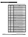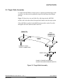
1
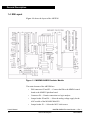
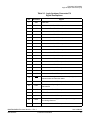
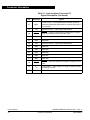
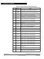
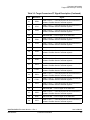
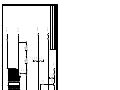
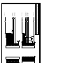
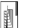
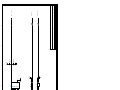
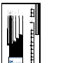
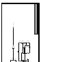
M68EML08AB32UM/D
REV. 1
M68EML08AB32
EMULATION MODULE
USER’S MANUAL
User’s Manual
Motorola reserves the right to make changes without further notice to
any products herein to improve reliability, function or design. Motorola
does not assume any liability arising out of the application or use of any
product or circuit described herein; neither does it convey any license
under its patent rights nor the rights of others. Motorola products are not
designed, intended, or authorized for use as components in systems
intended for surgical implant into the body, or other applications intended
to support or sustain life, or for any other application in which the failure
of the Motorola product could create a situation where personal injury or
death may occur. Should Buyer purchase or use Motorola products for
any such unintended or unauthorized application, Buyer shall indemnify
and hold Motorola and its officers, employees, subsidiaries, affiliates,
and distributors harmless against all claims, costs, damages, and
expenses, and reasonable attorney fees arising out of, directly or
indirectly, any claim of personal injury or death associated with such
unintended or unauthorized use, even if such claim alleges that Motorola
was negligent regarding the design or manufacture of the part.
© Motorola, Inc., 2000; All Rights Reserved
User’s Manual
2
M68EML08AB32 Emulator Module — Rev. 1
MOTOROLA
User’s Manual
User’s Manual
3
M68EML08AB32 Emulator Module — Rev. 1
MOTOROLA
User’s Manual — M68EML08AB32
List of Sections
Section 1. General Description . . . . . . . . . . . . . . . . . . . . . 9
Section 2. Configuration and Operation . . . . . . . . . . . . . 15
Section 3. Connector Information . . . . . . . . . . . . . . . . . . 19
Section 4. Schematics . . . . . . . . . . . . . . . . . . . . . . . . . . . 31
M68EML08AB32 Emulator Module — Rev. 1
MOTOROLA
User’s Manual
List of Sections
3
List of Sections
User’s Manual
4
M68EML08AB32 Emulator Module — Rev. 1
List of Sections
MOTOROLA
User’s Manual — M68EML08AB32
Table of Contents
Section 1. General Description
1.1
1.2
1.3
1.3.1
1.3.2
1.4
1.5
Contents . . . . . . . . . . . . . . . . . . . . . . . . . . . . . . . . . . . . . . . . . . . . . . . . 9
Introduction. . . . . . . . . . . . . . . . . . . . . . . . . . . . . . . . . . . . . . . . . . . . . . 9
Development Systems. . . . . . . . . . . . . . . . . . . . . . . . . . . . . . . . . . . . . 10
Motorola Modular Development System (MMDS). . . . . . . . . . . . 10
Motorola Modular Evaluation System (MMEVS). . . . . . . . . . . . . 11
EM Layout . . . . . . . . . . . . . . . . . . . . . . . . . . . . . . . . . . . . . . . . . . . . . 12
Specifications . . . . . . . . . . . . . . . . . . . . . . . . . . . . . . . . . . . . . . . . . . . 13
Section 2. Configuration and Operation
2.1
Contents . . . . . . . . . . . . . . . . . . . . . . . . . . . . . . . . . . . . . . . . . . . . . . . 15
2.2
Introduction. . . . . . . . . . . . . . . . . . . . . . . . . . . . . . . . . . . . . . . . . . . . . 15
2.3
Setting Jumper Headers . . . . . . . . . . . . . . . . . . . . . . . . . . . . . . . . . . . 16
2.3.1
Clock Source Header (P1) . . . . . . . . . . . . . . . . . . . . . . . . . . . . . . . 17
2.3.2
ADC Module Voltage Selector (P2 & P6). . . . . . . . . . . . . . . . . . . 17
2.4
Remaining System Installation . . . . . . . . . . . . . . . . . . . . . . . . . . . . . . 18
Section 3. Connector Information
3.1
3.2
3.3
3.4
3.5
Contents . . . . . . . . . . . . . . . . . . . . . . . . . . . . . . . . . . . . . . . . . . . . . . . 19
Introduction. . . . . . . . . . . . . . . . . . . . . . . . . . . . . . . . . . . . . . . . . . . . . 19
Logic Analyzer Connector (P4) . . . . . . . . . . . . . . . . . . . . . . . . . . . . . 20
Target Connectors (P7 and P8). . . . . . . . . . . . . . . . . . . . . . . . . . . . . . 23
Target Cable Assembly. . . . . . . . . . . . . . . . . . . . . . . . . . . . . . . . . . . . 29
Section 4. Schematics
Index
M68EML08AB32 Emulator Module — Rev. 1
MOTOROLA
User’s Manual
Table of Contents
5
Table of Contents
User’s Manual
6
M68EML08AB32 Emulator Module — Rev. 1
Table of Contents
MOTOROLA
User’s Manual — M68EML08AB32
Lists of Figures and Tables
Figure
Title
Page
Figure 1-1. M68EM08AB32 Emulator Module . . . . . . . . . . . . . . . . . . . . . . . 12
Figure 2-1. Jumper Header P1 . . . . . . . . . . . . . . . . . . . . . . . . . . . . . . . . . . . . 17
Figure 2-2. Jumper Header P2 . . . . . . . . . . . . . . . . . . . . . . . . . . . . . . . . . . . . 17
Figure 2-3. Jumper Header P6 . . . . . . . . . . . . . . . . . . . . . . . . . . . . . . . . . . . . 18
Figure 3-1. Logic Analyzer Connector P4 Pin Assignments . . . . . . . . . . . . . 20
Figure 3-2. Target Connectors P7 and P8 Pin Assignments. . . . . . . . . . . . . . 23
Figure 3-3. Target Cable Assembly . . . . . . . . . . . . . . . . . . . . . . . . . . . . . . . . 29
Table
Title
Page
Table 1-1. M68EM08AB32 Specifications . . . . . . . . . . . . . . . . . . . . . . . . . . 13
Table 2-1. Jumper Headers . . . . . . . . . . . . . . . . . . . . . . . . . . . . . . . . . . . . . . 16
Table 3-1. Logic Analyzer Connector P4 Signal Descriptions . . . . . . . . . . . 21
Table 3-2. Target Connectors P7 Signal Description . . . . . . . . . . . . . . . . . . . 24
Table 3-3. Target Connectors P8 Signal Descriptions . . . . . . . . . . . . . . . . . . 27
M68EML08AB32 Emulator Module — Rev. 1
MOTOROLA
Lists of Figures and Tables
User’s Manual
7
Lists of Figures and Tables
User’s Manual
8
M68EML08AB32 Emulator Module — Rev. 1
Lists of Figures and Tables
MOTOROLA
User’s Manual — M68EML08AB32
Section 1. General Description
1.1 Contents
1.2
Introduction. . . . . . . . . . . . . . . . . . . . . . . . . . . . . . . . . . . . . . . . . . . . . . 9
1.3
Development Systems. . . . . . . . . . . . . . . . . . . . . . . . . . . . . . . . . . . . . 10
1.3.1
Motorola Modular Development System (MMDS). . . . . . . . . . . . 10
1.3.2
Motorola Modular Evaluation System (MMEVS). . . . . . . . . . . . . 11
1.4
EM Layout . . . . . . . . . . . . . . . . . . . . . . . . . . . . . . . . . . . . . . . . . . . . . 12
1.5
Specifications . . . . . . . . . . . . . . . . . . . . . . . . . . . . . . . . . . . . . . . . . . . 13
1.2 Introduction
This user’s manual explains connection, configuration, and operation
information specific to the M68EML08AB32 emulator module (AB32EM).
The AB32EM lets you emulate and debug target systems based on the
MC68HC08AB16A and MC68HC908AB32 microcontroller units:
This section describes Motorola’s two development systems that use the
AB32EM, and it explains the AB32EM’s layout.
1.3 Development Systems
The AB32EM can be part of two Motorola development systems:
•
MMDS0508 Motorola Modular Development System (MMDS)
•
MMEVS0508 Motorola Modular Evaluation System (MMEVS)
M68EML08AB32 Emulator Module — Rev. 1
MOTOROLA
User’s Manual
General Description
9
General Description
1.3.1 Motorola Modular Development System (MMDS)
The MMDS is an emulator system that provides a bus state analyzer and
real-time memory windows. The unit’s integrated design environment includes
an editor, an assembler, user interface, and source-level debug.
A complete MMDS consists of:
•
Station module — The metal MMDS enclosure containing the control
board and the internal power supply
•
Emulator module (EM) — A separately purchased printed circuit board
that enables system functionality for a specific set of microcontroller
units
•
Two logic clip cable assemblies — Twisted-pair cables that connect the
station module to the target system, a test fixture, a clock, an oscillator,
or any other circuitry useful for evaluation or analysis. One end of each
cable assembly has a molded connector, which fits into station-module
pod A or pod B. Leads at the other end of each cable terminate in female
probe tips. Ball clips come with the cable assemblies.
•
9-lead RS-232 serial cable — Cable that connects the station module to
the host computer RS-232 port
•
9- to 25-pin adapter — A molded assembly that connects the 9-pin cable
to a 25-pin serial port
•
System software — MCUez™ software on CD-ROM and P&E
Microcomputer System, Inc. software on CD-ROM
•
MMDS documentation — MMDS Operations Manual, Motorola
document order number MMDS0508OM/D; the MCUez software
manual, included with the MCUez software package; a system software
manual, included with the P&E Microcomputer System, Inc.’s
MMDS0508 software package; and this EM user's manual (this manual)
MMDS baud rates are selected by the user at 2400, 4800, 9600, 19,200, 38,400,
or 57,600.
As mentioned, the AB32EM gives the MMDS the ability to emulate target
systems based on MC68HC08AB16A and MC68HC908AB32 microcontroller
units. By substituting a different EM, MMDS can be enabled to emulate target
User’s Manual
10
M68EML08AB32 Emulator Module — Rev. 1
General Description
MOTOROLA
General Description
Development Systems
systems based on a different MCU. (A local Motorola representative can
explain all the EMs available.)
1.3.2 Motorola Modular Evaluation System (MMEVS)
An MMEVS is an economical, two-board tool for designing, debugging, and
evaluating target systems based on MC68HC05 or MC68HC08 MCUs.
A complete MMEVS consists of:
•
Platform board (PFB) — The bottom board, which supports the emulator
module; has connectors for power and for a terminal or host computer
•
Emulator module (EM) — A separately purchased printed circuit board
that enables system functionality for a specific set of MCUs; fits onto
the PFB
•
RS-232 serial cable — A separately purchased cable that connects the
PFB to the host computer RS-232 port
•
System software — MCUez™ software on CD-ROM and P&E
Microcomputer System, Inc. software on CD-ROM
•
MMEVS documentation — MMEVS Operations Manual, Motorola
document order number MMEVSOM/D; the MCUez software manual,
included with the MCUez software package; a system software manual,
included with the P&E Microcomputer System, Inc.’s MMDS0508
software package; and this emulator user's manual
An MMEVS features automatic selection of the communication baud rate from
these choices: 2400, 4800, 9600, 19,200, 38,400, or 57,600.
With a AB32EM, the MMEVS emulates target systems based on
MC68HC908AB32 MCUs. By substituting a different EM, the MMEVS can be
enabled to emulate target systems based on a different MCU. (A local Motorola
representative can explain all the EMs available.)
Section 2. Configuration and Operation explains how to configure and use
the AB32EM as part of an MMDS or MMEVS system.
M68EML08AB32 Emulator Module — Rev. 1
MOTOROLA
User’s Manual
General Description
11
General Description
1.4 EM Layout
Figure 1-1 shows the layout of the AB32EM.
Figure 1-1. M68EML08AB32 Emulator Module
The main elements of the AB32EM are:
•
DIN connectors P3 and P5 — Connect the EM to the MMDS control
board or the MMEVS platform board
•
Connector P4 — Permits connection to a logic analyzer
•
Jumper header P2 and P6 — Select the analog voltage supply for the
ADC module of the MC68HC908AB32.
•
Jumper header P1 — Selects the MCU clock source
User’s Manual
12
M68EML08AB32 Emulator Module — Rev. 1
General Description
MOTOROLA
General Description
Specifications
•
Connectors P7 and P8 — Customer-specific interfaces to the target
system
The AB32EM requires a user-supplied 80-lead target cable and target head
adapter to connect the target system to connectors P7 and P8.
1.5 Specifications
Table 1-1 lists AB32EM specifications.
Table 1-1. M68EML08AB32 Specifications
Characteristics
Specifications
MCU extension I/O ports
HCMOS compatible
Operating temperature
0° to 40°C
Storage temperature
–40° to +85°C
Relative humidity
0 to 90% (non-condensing)
Power requirements
+5 V dc and +12 V dc (charge pump), provided from
the MMDS control board or MMEVS platform board
Dimensions
8.2 x 5.5 inches; 207 x 140 mm
Weight
7.62 ounces; 216 grams
M68EML08AB32 Emulator Module — Rev. 1
MOTOROLA
User’s Manual
General Description
13
General Description
User’s Manual
14
M68EML08AB32 Emulator Module — Rev. 1
General Description
MOTOROLA
User’s Manual — M68EML08AB32
Section 2. Configuration and Operation
2.1 Contents
2.2
Introduction. . . . . . . . . . . . . . . . . . . . . . . . . . . . . . . . . . . . . . . . . . . . . 15
2.3
Setting Jumper Headers . . . . . . . . . . . . . . . . . . . . . . . . . . . . . . . . . . . 16
2.3.1
Clock Source Header (P1) . . . . . . . . . . . . . . . . . . . . . . . . . . . . . . . 17
2.3.2
ADC Module Voltage Selector (P2 & P6). . . . . . . . . . . . . . . . . . . 17
2.4
Remaining System Installation . . . . . . . . . . . . . . . . . . . . . . . . . . . . . . 18
2.2 Introduction
This section explains configuration and operation of the AB32EM when it is
installed in an MMDS (Motorola modular development system) or MMEVS
(Motorola modular evaluation system). For other parts of system installation or
configuration, see the MMDS or MMEVS hardware manuals.
NOTE:
An AB32EM already installed in an MMDS station module can be reconfigured.
To do so, switch off station-module power, then follow the guidance in this
section. Similarly, AB32EM that is already installed on the MMEVS platform
board can be reconfigured, provided that platform-board power is
disconnected.
CAUTION:
Be sure to switch off or disconnect power when reconfiguring an installed EM.
Reconfiguring EM jumper headers with the power on can damage system
circuits.
M68EML08AB32 Emulator Module — Rev. 1
MOTOROLA
Configuration and Operation
User’s Manual
15
Configuration and Operation
ESD CAUTION:
Ordinary amounts of static electricity from clothing or the work environment
can damage or degrade electronic devices and equipment. For example, the
electronic components installed on printed circuit boards are extremely
sensitive to electrostatic discharge (ESD). Wear a ground wrist strap whenever
handling any printed circuit board. This strap provides a conductive path for
safely discharging static electricity to ground.
2.3 Setting Jumper Headers
The AB32EM has three jumper headers. Table 2-1 contains a summary of
settings for these headers. Paragraphs 2.3.1 Clock Source Header (P1) and
2.3.2 ADC Module Voltage Selector (P2 & P6) give additional information
about each jumper header.
Table 2-1. Jumper Headers
Jumper
Header
P1
P2
P6
User’s Manual
16
Type
1
3
1
3
1
3
Description
2
4
2
4
2
4
Jumper between pins 1 and 2 (factory default); selects
the clock signal from the MMDS control board or
MMEVS platform board as the OSC1 input signal
Jumper between pins 3 and 4; selects the target system
clock as the OSC1 input signal
Jumper between pins 1 and 2; selects the target system
as the analog voltage source, VDDAREF, as input for
the MC68HC908AB32 ADC module
Jumper between pins 3 and 4 (factory default); selects
on-board, isolated analog voltage source, LVDD, as
input for the MC68HC908AB32 ADC module
Jumper between pins 1 and 2; selects the target system
as the analog ground source, AVSS/VREFL, as input
for the MC68HC908AB32 ADC module
Jumper between pins 3 and 4 (factory default); selects
on-board ground, GND, as input for the
MC68HC908AB32 ADC module
M68EML08AB32 Emulator Module — Rev. 1
Configuration and Operation
MOTOROLA
Configuration and Operation
Setting Jumper Headers
2.3.1 Clock Source Header (P1)
Use jumper header P1 (shown in Figure 2-1) to determine the clock signal
source. The factory configuration (the fabricated jumper between pins 1 and 2)
selects the clock signal from the MMDS control board or MMEVS platform
board.
Figure 2-1. Jumper Header P1
P1
MMDS
1
•
•
2
OSC1
3
•
•
4
Alternately, the target system clock signal source can be selected, as shown in
Figure 2-1. To select the target system as the clock source, install the fabricated
jumper between pins 3 and 4. Ensure that the clock source (OSC1) is connected
to the EM via the target cable, connector P8 pin 7.
NOTE:
Only one jumper should be inserted on jumper header P1 at a time. Inserting
multiple jumpers in P1 may damage the AB32EM.
2.3.2 ADC Module Voltage Selector (P2 & P6)
Use jumper header P2 to select the on-board LVDD or an external analog
voltage supply as the supply connection for the MC68HC908AB32 ADC
convertor.
Figure 2-2 shows the default factory jumper header configuration, which has a
fabricated jumper installed on jumper header P2 between pins 3 and 4.
P2
VDDAREF
1
•
•
2
LVDD
3
•
•
4
Figure 2-2. Jumper Header P2
M68EML08AB32 Emulator Module — Rev. 1
MOTOROLA
Configuration and Operation
User’s Manual
17
Configuration and Operation
Use jumper header P6 to select the on-board GND or the external analog ground
as the ground connection for the MC68HC908AB32 ADC convertor.
Figure 2-3 shows the default factory jumper header configuration, which has a
fabricated jumper installed on jumper header P6 between pins 3 and 4.
P6
AVSS/VREFL
1
•
•
2
GND
3
•
•
4
Figure 2-3. Jumper Header P6
2.4 Remaining System Installation
When all jumper headers are configured, follow these steps to complete the
AB32EM installation:
•
To install the AB32EM in an MMDS station module, remove the entire
top half of the station-module enclosure. Fit together EM connectors P3
and P5 (on the bottom of the board) and control-board connectors P1 and
P2. Snap the corners of the EM onto the plastic standoffs.
•
To install the AB32EM on an MMEVS platform board, fit together EM
connectors P3 and P5 (on the bottom of the board) and platform-board
connectors P3 and P4. Snap the corners of the EM onto the plastic
standoffs.
•
Copy the personality file from the provided P&E CD-ROM or the
CD-ROM that contains the technical documentation,
M69EML08AB32/CD, to the directory that contains the debugging
software. The personality files for the AB32EM are:
–
AB16AVxx.MEM - MC68HC908AB16A MCU (MCUez/P&E)
–
00C58Vxx.MEM - MC68HC908AB32 MCU (MCUez)
–
00458Vxx.MEM - MC68HC908AB32 MCU (P&E)
At this point, make any system cable connections and restore power. For
instructions, consult the MMDS or MMEVS operations manuals.
User’s Manual
18
M68EML08AB32 Emulator Module — Rev. 1
Configuration and Operation
MOTOROLA
User’s Manual — M68EML08AB32
Section 3. Connector Information
3.1 Contents
3.2
Introduction. . . . . . . . . . . . . . . . . . . . . . . . . . . . . . . . . . . . . . . . . . . . . 19
3.3
Logic Analyzer Connector (P4) . . . . . . . . . . . . . . . . . . . . . . . . . . . . . 20
3.4
Target Connectors (P7 and P8). . . . . . . . . . . . . . . . . . . . . . . . . . . . . . 23
3.5
Target Cable Assembly. . . . . . . . . . . . . . . . . . . . . . . . . . . . . . . . . . . . 28
3.2 Introduction
This section consists of pin assignments and signal descriptions for
M68EML08AB32 target and logic analyzer connectors.
M68EML08AB32 Emulator Module — Rev. 1
MOTOROLA
User’s Manual
Connector Information
19
Connector Information
3.3 Logic Analyzer Connector (P4)
Connector P4 is the AB32EM logic analyzer connector.
Figure 3-1 shows the pin assignments for connector P4. Table 3-1 gives the
signal descriptions.
P4
GND
1
• •
2
LA15
AD7
3
• •
4
LA14
AD6
5
• •
6
LA13
AD5
7
• •
8
LA12
AD4
9
• •
10
LA11
AD3
11 • •
12
LA10
AD2
13
• •
14
LA9
AD1
15
• •
16
LA8
AD0
17
• •
18
LA7
LIR
19
• •
20
LA6
R/W
21
• •
22
LA5
GND
23
• •
24
LA4
PHI2
25
• •
26
LA3
LBOX
27
• •
28
LA2
BREAK
29
• •
30
LA1
GND
31
• •
32
LA0
GND
33
• •
34
GND
GND
35
• •
36
GND
GND
37
• •
38
RESET
VDD
39
• •
40
GND
Figure 3-1. Logic Analyzer Connector P4 Pin Assignments
User’s Manual
20
M68EML08AB32 Emulator Module — Rev. 1
Connector Information
MOTOROLA
Connector Information
Logic Analyzer Connector (P4)
Table 3-1. Logic Analyzer Connector P4
Signal Descriptions
Pin
Mnemonic
Signal
1
GND
GROUND
2
LA15
Address bus bit 15 — MCU output address bus
3
AD7
Data bus bit 7 — MCU bidirectional data bus
4
LA14
Address bus bit 15 — MCU output address bus
5
AD6
Data bus bit 6 — MCU bidirectional data bus
6
LA13
Address bus bit 13 — MCU output address bus
7
AD5
Data bus bit 5 — MCU bidirectional data bus
8
LA12
Address bus bit 12 — MCU output address bus
9
AD4
Data bus bit 4 — MCU bidirectional data bus
10
LA11
Address bus bit 11 — MCU output address bus
11
AD3
Data bus bit 3 — MCU bidirectional data bus
12
LA10
Address bus bit 10 — MCU output address bus
13
AD2
Data bus bit 2 — MCU bidirectional data bus
14
LA9
Address bus bit 9 — MCU output address bus
15
AD1
Data bus bit 1 — MCU bidirectional data bus
16
LA8
Address bus bit 8 — MCU output address bus
17
AD0
Data bus bit 0 — MCU bidirectional data bus
18
LA7
Address bus bit 7 — MCU output address bus.
19
LIR
Load instruction register — Active-low output signal,
asserted when an instruction starts
20
LA6
Address bus bit 6 — MCU output address bus
21
R/W
Read/Write — Output signal that indicates the direction of
data transfer
22
LA5
Address bus bit 5 — MCU output address bus
23
GND
GROUND
24
LA4
Address bus bit 4 — MCU output address bus
25
PHI2
PHI2 clock — Internally generated output clock signal used
as a timing reference
26
LA3
Address bus bit 3 — MCU output address bus
M68EML08AB32 Emulator Module — Rev. 1
MOTOROLA
User’s Manual
Connector Information
21
Connector Information
Table 3-1. Logic Analyzer Connector P4
Signal Descriptions (Continued)
Pin
Mnemonic
Signal
27
LBOX
Last bus cycle — Input signal that the emulator asserts to
indicate that the target system MCU is in the last bus cycle of
an instruction
28
LA2
29
BREAK
30
LA1
Address bus bit 1 — MCU output address bus
31
GND
GROUND
32
LA0
Address bus bit 0 — MCU output address bus
33
GND
GROUND
34
GND
GROUND
35
GND
GROUND
36
GND
GROUND
37
GND
GROUND
38
RESET
RESET — Active-low bidirectional signal for starting an EVS
reset
39
VDD
+5 Vdc power — Input voltage (+5 Vdc @ 1A (max)) used by
the EM logic circuits
40
GND
GROUND
Address bus bit 2 — MCU output address bus
BREAK — Active low signal that the EM asserts to stop the
target system MCU from running user code
User’s Manual
22
M68EML08AB32 Emulator Module — Rev. 1
Connector Information
MOTOROLA
Connector Information
Target Connectors (P7 and P8)
3.4 Target Connectors (P7 and P8)
AB32EM has two target connectors: P7 and P8, each a 2-row by 20-pin
connector.
Figure 3-2, Table 3-2, and Table 3-3 give the pin assignments and signal
descriptions for these connectors.
P7
P8
GND
1
• •
2
IRQ
PTC5 1
• •
2
PTC4
PTC2
3
• •
4
GND
PTC3 3
• •
4
RESET
PTC0
5
• •
6
PTF1
PTC1 5
• •
6
PTF0
NC
7
• •
8
PTF3
OSC1
7
• •
8
PTF2
VDD
9
• •
10
NC
GND
9
• •
10
PTF4
LVDD
11
• •
12
PTF5
GND
11
• •
12
PTF7
PTD7
13
• •
14
PTB7
VREFH
13
• •
14
GND
PTD5
15
• •
16
PTD1
PTD6 15
• •
16
PTD0
PTH1
17
• •
18
AVSS/VREFL
PTD4 17
• •
18
VDDAREF
GND
19
• •
20
PTD3
PTH0 19
• •
20
PTD2
PTB2
21
• •
22
PTA7
PTB1
21
• •
22
PTB0
PTB4
23
• •
24
GND
PTB3
23
• •
24
PTA6
PTB6
25
• •
26
PTA4
PTB5
25
• •
26
PTA5
NC
27
• •
28
PTA2
GND
27
• •
28
PTA3
NC
29
• •
30
PTA0
NC
29
• •
30
PTA1
PTF6
31
• •
32
PTG2
NC
31
• •
32
GND
PTE1
33
• •
34
PTG0
PTE0
33
• •
34
PTG1
PTE3
35
• •
36
GND
PTE2
35
• •
36
EVDD
PTE5
37
• •
38
GND
PTE4
37
• •
38
GND
PTE7
39
• •
40
GND
PTE6
39
• •
40
GND
Figure 3-2. Target Connectors P7 and P8 Pin Assignments
M68EML08AB32 Emulator Module — Rev. 1
MOTOROLA
User’s Manual
Connector Information
23
Connector Information
Table 3-2. Target Connectors P7 Signal Description
Pin
Mnemonic
Signal
1
GND
EM GROUND — Ground signal of the EM board
2
IRQ
INTERRUPT REQUEST — Active-low input line for
requesting MCU asynchronous non-maskable interrupt
3
PTC2
PORT C (bit 2) — General-purpose I/O lines controlled by
software via data direction and data registers
4
GND
EM GROUND — Ground signal of the EM board
5
PTC0
PORT C (bit 0) — General-purpose I/O lines controlled by
software via data direction and data registers
6
PTF1
PORT F (bit 1) — General-purpose I/O lines controlled by
software via data direction and data registers
7
NC
8
PTF3
9
VDD
MMDS +5 V — Used for factory testing
10
NC
No connect
11
LVDD
AB32 EM Voltage high — Used for factory testing
12
PTF5
PORT F (bit 5) — General-purpose I/O lines controlled by
software via data direction and data registers
13
PTD7
PORT D (bit 7) — General-purpose I/O lines controlled by
software via data direction and data registers
14
PTB7
PORT B (bit 7) — General-purpose I/O lines controlled by
software via data direction and data registers
15
PTD5
PORT D (bit 5) — General-purpose I/O lines controlled by
software via data direction and data registers
16
PTD1
PORT D (bit 1) — General-purpose I/O lines controlled by
software via data direction and data registers
17
PTH1
PORT H (bit 1) — General-purpose I/O lines controlled by
software via data direction and data registers
18
AVSS/VREFL
Analog ground pin for ADC convertor and the ADC voltage
referance low
19
GND
EM GROUND — Ground signal of the EM board
20
PTD3
PORT D (bit 3) — General-purpose I/O lines controlled by
software via data direction and data registers
No connect
PORT F (bit 3) — General-purpose I/O lines controlled by
software via data direction and data registers
User’s Manual
24
M68EML08AB32 Emulator Module — Rev. 1
Connector Information
MOTOROLA
Connector Information
Target Connectors (P7 and P8)
Table 3-2. Target Connectors P7 Signal Description (Continued)
Pin
Mnemonic
Signal
21
PTB2
PORT B (bit 2) — General-purpose I/O lines controlled by
software via data direction and data registers
22
PTA7
PORT A (bit 7) — General-purpose I/O lines controlled by
software via data direction and data registers
23
PTB4
PORT B (bit 4) — General-purpose I/O lines controlled by
software via data direction and data registers
24
GND
EM GROUND — Ground signal of the EM board
25
PTB6
PORT B (bit 6) — General-purpose I/O lines controlled by
software via data direction and data registers
26
PTA4
PORT A (bit 4) — General-purpose I/O lines controlled by
software via data direction and data registers
27
NC
28
PTA2
29
NC
30
PTA0
PORT A (bit 0) — General-purpose I/O lines controlled by
software via data direction and data registers
31
PTF6
PORT F (bit 6) — General-purpose I/O lines controlled by
software via data direction and data registers
32
PTG2
PORT G (bit 2) — General-purpose I/O lines controlled by
software via data direction and data registers
33
PTE1
PORT E (bit 1) — General-purpose I/O lines controlled by
software via data direction and data registers
34
PTG0
PORT G (bit 0) — General-purpose I/O lines controlled by
software via data direction and data registers
35
PTE3
PORT E (bit 3) — General-purpose I/O lines controlled by
software via data direction and data registers
36
GND
EM GROUND — Ground signal of the EM board
37
PTE5
PORT E (bit 5) — General-purpose I/O lines controlled by
software via data direction and data registers
38
GND
EM GROUND — Ground signal of the EM board
39
PTE7
PORT E (bit 7) — General-purpose I/O lines controlled by
software via data direction and data registers
No connect
PORT A (bit 2) — General-purpose I/O lines controlled by
software via data direction and data registers
No connect
M68EML08AB32 Emulator Module — Rev. 1
MOTOROLA
User’s Manual
Connector Information
25
Connector Information
Table 3-2. Target Connectors P7 Signal Description (Continued)
Pin
Mnemonic
40
GND
Signal
EM GROUND — Ground signal of the EM board
User’s Manual
26
M68EML08AB32 Emulator Module — Rev. 1
Connector Information
MOTOROLA
Connector Information
Target Connectors (P7 and P8)
Table 3-3. Target Connectors P8 Signal Descriptions
Pin
Mnemonic
Signal
1
PTC5
PORT C (bit 5) — General-purpose I/O lines controlled by
software via data direction and data registers
2
PTC4
PORT C (bit 4) — General-purpose I/O lines controlled by
software via data direction and data registers
3
PTC3
PORT C (bit 3) — General-purpose I/O lines controlled by
software via data direction and data registers
4
RESET
5
PTC1
PORT C (bit 1) — General-purpose I/O lines controlled by
software via data direction and data registers
6
PTF0
PORT F (bit 0) — General-purpose I/O lines controlled by
software via data direction and data registers
7
OSC1
OSCILLATOR — Crystal oscillator amplifier input signal
8
PTF2
PORT F (bit 2) — General-purpose I/O lines controlled by
software via data direction and data registers
9
GND
EM GROUND — Ground signal of the EM board
10
PTF4
PORT F (bit 4) — General-purpose I/O lines controlled by
software via data direction and data registers
11
GND
EM GROUND — Ground signal of the EM board
12
PTF7
PORT F (bit 7) — General-purpose I/O lines controlled by
software via data direction and data registers
13
VREFH
14
GND
EM GROUND — Ground signal of the EM board
15
PTD6
PORT D (bit 6) — General-purpose I/O lines controlled by
software via data direction and data registers
16
PTD0
PORT D (bit 0) — General-purpose I/O lines controlled by
software via data direction and data registers
17
PTD4
PORT D (bit 4) — General-purpose I/O lines controlled by
software via data direction and data registers
18
VDDAREF
19
PTH0
PORT H (bit 0) — General-purpose I/O lines controlled by
software via data direction and data registers
20
PTD2
PORT D (bit 2) — General-purpose I/O lines controlled by
software via data direction and data registers
RESET — Active-low bidirectional control line that
initializes the MCU
ADC voltage reference high
Analog supply pin for ADC convertor
M68EML08AB32 Emulator Module — Rev. 1
MOTOROLA
User’s Manual
Connector Information
27
Connector Information
Table 3-3. Target Connectors P8 Signal Descriptions (Continued)
Pin
Mnemonic
Signal
21
PTB1
PORT B (bit 1) — General-purpose I/O lines controlled by
software via data direction and data registers
22
PTB0
PORT B (bit 0) — General-purpose I/O lines controlled by
software via data direction and data registers
23
PTB3
PORT B (bit 3) — General-purpose I/O lines controlled by
software via data direction and data registers
24
PTA6
PORT A (bit 6) — General-purpose I/O lines controlled by
software via data direction and data registers
25
PTB5
PORT B (bit 5) — General-purpose I/O lines controlled by
software via data direction and data registers
26
PTA5
PORT A (bit 5) — General-purpose I/O lines controlled by
software via data direction and data registers
27
GND
EM GROUND — Ground signal of the EM board
28
PTA3
PORT A (bit 3) — General-purpose I/O lines controlled by
software via data direction and data registers
29
NC
30
PTA1
31
NC
32
GND
EM GROUND — Ground signal of the EM board
33
PTE0
PORT E (bit 0) — General-purpose I/O lines controlled by
software via data direction and data registers
34
PTG1
PORT G (bit 1) — General-purpose I/O lines controlled
by software via data direction and data registers
35
PTE2
PORT E (bit 2) — General-purpose I/O lines controlled by
software via data direction and data registers
36
EVDD
Target system Voltage high
37
PTE4
PORT E (bit 4) — General-purpose I/O lines controlled by
software via data direction and data registers
38
GND
EM GROUND — Ground signal of the EM board
39
PTE6
PORT E (bit 6) — General-purpose I/O lines controlled by
software via data direction and data registers
40
GND
EM GROUND — Ground signal of the EM board
No connect
PORT A (bit 1) — General-purpose I/O lines controlled by
software via data direction and data registers
No connect
User’s Manual
28
M68EML08AB32 Emulator Module — Rev. 1
Connector Information
MOTOROLA
Connector Information
Target Cable Assembly
3.5 Target Cable Assembly
To connect the AB32EM to a target system, a separately purchased target cable
assembly is needed, plus the appropriate target head and target-head/adapter
package.
Figure 3-3 shows how one end of the flex cable plugs into the AB32EM
module, and it also shows how the target head connects into the target system.
If the AB32EM is installed in the MMDS station module, run the flex cable
through the slit in the station-module enclosure.
EMULATOR
TERMINATOR
HEAD
TERMINATOR
CONNECTS TO
TARGET HEAD
TARGET
CABLE
CONNECTS TO EM
TARGET CONNECTORS
TARGET HEAD
PLUGS TO TARGET SYSTEM MCU
SOCKET OR SURFACE MOUNT ADAPTER
Figure 3-3. Target Cable Assembly
M68EML08AB32 Emulator Module — Rev. 1
MOTOROLA
User’s Manual
Connector Information
29
Connector Information
User’s Manual
30
M68EML08AB32 Emulator Module — Rev. 1
Connector Information
MOTOROLA
User’s Manual — M68EML08AB32
Section 4. Schematics
This chapter contains the M68EML08AB32 emulator module schematic
diagrams.
These schematic diagrams are for reference only and may deviate slightly from
the circuits on the AB32EM.
M68EML08AB32 Emulator Module — Rev. 1
MOTOROLA
User’s Manual
Schematics
31
1
2
3
DIEN*
AD[0..7]
A
AD7
AD6
AD5
AD4
AD3
AD2
AD1
AD0
18
17
16
15
14
13
12
11
G
DIR
A1
A2
A3
A4
A5
A6
A7
A8
74AC245
B1
B2
B3
B4
B5
B6
B7
B8
U8
B
19
1
2
3
4
5
6
7
8
9
B
VDD
1
2
3
4
5
6
7
8
9
8
10
Q26-3
9
13
C
MPQ2369
4.7k
7
RP7
5
Q26-2
6
MPQ2369
13
8
10
Q24-3
D
MPQ2369
MPQ2369
12
14
Q24-4
MPQ2369
3
1
Q26-1
9
8
7
6
5
4
3
2
MPQ2369
12
14
Q26-4
4.7k
RP4
1
LVDD
D
9
C
5
Q24-2
6
2
MPQ2369
MPQ2369
3
1
Q24-1
7
10
Q22-3
9
13
E
MPQ2369
MPQ2369
12
14
Q22-4
8
E
3
2
6
MPQ2369
1
5
Q22-2
MPQ2369
Q22-1
7
10
Q15-3
9
13
MPQ2369
F
MPQ2369
12
14
Q15-4
8
F
LVDD
3
7
Q15-2
5
4K7
RP5
LVDD
G
G
Tuesday, February 22, 2000
Date:
Kelvin Tse
Designed By:
Sheet
Approved By:
M68EML08AB32 EMULAOTR MODULE (AD bus buffer)
MCU_PTA7
MCU_PTA6
MCU_PTA5
MCU_PTA4
MCU_PTA3
MCU_PTA2
MCU_PTA1
MCU_PTA0
3.3k
RP6
Size
B
Title
!MOTOROLA
MPQ2369
MPQ2369
1
Q15-1
2
4
A
2
1
9
8
7
6
5
4
3
2
6
1
9
8
7
6
5
4
3
2
1
H
of
13
Rev
A
MCU_PTA[0..7]
Edward Chui
H
1
2
3
4
1
2
3
4
SCLK
AD[0..7]
A
MCU_PTB[0..7]
A
B
B
RP2
2
3
4
5
6
7
8
9
MCU_PTB0
MCU_PTB1
MCU_PTB2
MCU_PTB3
MCU_PTB4
MCU_PTB5
MCU_PTB6
MCU_PTB7
10k
1
LVDD
3
2
1
C
5
Q5-1
MPQ2369
C
7
2
3
6
5
9
AD7
AD6
AD5
AD4
AD3
AD2
AD1
AD0
10
D
13
12
9
D
10
8
13
11
1
2
3
4
5
6
7
8
9
14
74AC573
Q1
Q2
Q3
Q4
Q5
Q6
Q7
Q8
19
18
17
16
15
14
13
12
Q5-4
MPQ2369
C
OC
D1
D2
D3
D4
D5
D6
D7
D8
U5
12
Q5-3
MPQ2369
14
Q6-4
MPQ2369
8
Q6-3
MPQ2369
7
Q6-2
MPQ2369
1
Q6-1
MPQ2369
Q5-2
MPQ2369
6
1k
E
VDD
1
RP1
E
LA7
LA6
LA5
LA4
LA3
LA2
LA1
LA0
2
3
4
5
6
7
8
9
F
F
9
8
7
6
5
4
3
2
19
1
Y8
Y7
Y6
Y5
Y4
Y3
Y2
Y1
11
12
13
14
15
16
17
18
LA8
LA9
LA10
LA11
LA12
LA13
LA14
LA15
G
Monday, February 21, 2000
Date:
KELVIN TSE
Designed By:
Sheet
Approved By:
M68EM08AB32 EMULATOR MODULE (Address bus buffer)
Size
B
Title
!MOTOROLA
74AC541
A8
A7
A6
A5
A4
A3
A2
A1
G2
G1
U3
G
2
H
of
13
Edward Chui
LA[0..15]
LA[0..15]
H
Rev
A
1
2
3
4
B
C
3
Q18
2N5458
D
6
11
10
9
5
3
2
1
12
13
X
VEE
Z
Y
74HC4053
INH
A
B
C
Z0
Z1
Y0
Y1
X0
X1
U13
7
4
15
14
E
E
F
F
!MOTOROLA
G
Edward Chui
PTC2
H
Rev
A
3
4
G
Tuesday, February 22, 2000
Date:
Kelvin Tse
Designed By:
Sheet
Approved By:
M68EML08AB32 EMULATOR MODULE (CLOCK INPUT)
Size
B
Title
3
H
of
13
1
A
1
Q25-1
MPQ2369
2
1
LVDD
D
1
3
1K
R37
C
2
PC2
PTC2_CLKON
SCLK*
B
2
3
4
A
2
1
2
1
2
3
VSSAD
VDDAD
VREFH
PTG[0..2]
PTE[0..7]
PTF[0..7]
A
+
B
C42
47uF
C40
0.01uF
C36
0.1uF
1
2
+
C
C39
47uF
C
C35
0.01uF
1
2
FERRITE_BEAD L2
PTG0
PTG1
PTG2
PTF7
PTF5
PTF6
PTE0
PTE1
PTE2
PTE3
PTE4
PTE5
PTE6
PTE7
PTF0
PTF1
PTF2
PTF3
PTF4
2
1
2
3
4
5
6
7
8
9
10
11
12
13
14
15
16
17
18
19
20
21
22
23
24
25
26
27
28
29
30
31
32
D
47uF
C29
0.01uF
PTC5
PTC3
PTC2/MCLK
PTC1
PTC0
OSC1
OSC2
CGMXFC
VSSA
VDDA
VREFH
PTD7
PTD6/TACLK
PTD5
PTD4/TBCLK
PTH1/KBD4
PTH0/KBD3
PTD3
PTD2
VSSAD
VDDAD
PTD1
PTD0
PTB7/ATD7
PTB6/ATD6
PTB5/ATD5
PTB4/ATD4
PTB3/ATD3
PTB2/ATD2
PTB1/ATD1
PTB0/ATD0
PTA7
+ C31
LVDD
MC68HC908AB32FU
PTC4
IRQ1
RST
PTF0/TACH2
PTF1/TACH3
PTF2/TBCH2
PTF3/TBCH3
PTF4/TBCH0
NC
PTF7
PTF5/TBCH1
PTF6
PTE0/TxD
PTE1/RxD
PTE2/TACH0
PTE3/TACH1
PTE4/SS
PTE5/MISO
PTE6MOSI
PTE7/SPSCK
VSS
VDD
PTG0/KBD0
PTG1/KBD1
PTG2/KBD2
PTA0
PTA1
PTA2
PTA3
PTA4
PTA5
PTA6
U15
FERRITE_BEAD
L1
LVDD
1
64
63
62
61
60
59
58
57
56
55
54
53
52
51
50
49
48
47
46
45
44
43
42
41
40
39
38
37
36
35
34
33
E
L4
C33
0.1uF
L3
FERRITE_BEAD
LVDD
2
1
E
2
FERRITE_BEAD
PA7
PA6
PA5
PA4
PA3
PA2
PA1
PA0
C34
47uF0.1uF
C41
PTD1
PTD0
MCU_PTB7
MCU_PTB6
MCU_PTB5
MCU_PTB4
MCU_PTB3
MCU_PTB2
MCU_PTB1
MCU_PTB0
PTD7
PTD6
PTD5
PTD4
PTH1
PTH0
PTD3
PTD2
1
1
2
1
2
D
1
2
2
1
MCU_PTC4
MCUIRQ*
MCURST*
1
2
B
1
2
1
2
F
0.01uF
C38
F
19
1
2
3
4
5
6
7
8
9
B1
B2
B3
B4
B5
B6
B7
B8
18
17
16
15
14
13
12
11
R45
G
Tuesday, February 22, 2000
Date:
Kelvin Tse
Designed By:
R44
Sheet
Approved By:
1K
LVDD
M68EML08AB32 EMULATOR MODULE (CPU)
MPQ2369
7 Q25-2
6
5
1K
LVDD
MCU_PTA7
MCU_PTA6
MCU_PTA5
MCU_PTA4
MCU_PTA3
MCU_PTA2
MCU_PTA1
MCU_PTA0
Size
B
Title
!MOTOROLA
74AC245
G
DIR
A1
A2
A3
A4
A5
A6
A7
A8
U14
G
2
1
4
A
1
2
1
2
1
2
2
1
+
4
H
of
13
Edward Chui
DIEN*
MCU_PTA[0..7]
MCU_PTB[0..7]
VSSAD
VDDAD
PTH[0..1]
VREFH
MCU_PTC5
MCU_PTC3
MCLK
MCU_PTC1
MCU_PTC0
MCU_OSC
PTD[0..7]
H
Rev
A
1
2
3
4
1
2
3
A
OSC1
MMDSOSC
MCLK
MCU_PTC1
MCU_PTC0
SCLK_6
5
R33
VDD
7
1
1K
B
74AC14
2
12
R34
U6A
Q17-2
MPQ2369
1K
LVDD
1
2
BREAK*
B
R31
14
3
1K
74AC14
10
R29
U6B
VDD
Q17-4
MPQ2369
1K
LVDD
1
2
4
1
2
6
1
2
13
C
4
R32
2
1
8
5
VDD
Q17-3
MPQ2369
1K
LVDD
C
1
2
9
A
74AC14
U6C
3
6
Q16
2N5458
9
D
9
74AC04
U9D
D
8
5
74AC14
U6D
8
74AC04
U9C
1
3
P1
2
4
OSC SELECT
6
13
E
74AC04
10
R43
8
Q23-3
MPQ2369
1K
LVDD
10
12
74AC04
U9E
U9F
11
E
2
1
9
3
74AC04
U9B
2
1
2
R35
1
F
4
3
3
1K
R42
MPQ2369
5
Q23-27
2
1
LVDD
2
1
LVDD
3
Q21
2N5458
3
Q19
2N5458
G
G
Tuesday, February 22, 2000
Date:
C.C. Poon
Designed By:
Size
B
Sheet
Approved By:
H
MCU_OSC
SCLK*
SCLK
SIMRW
SIMLIR*
MCU_PTC4
MCU_PTC3
5
H
of
13
Edward Chui
M68EML08AB32 EMULATOR MODULE (CPU port C buffer and OSC)
!MOTOROLA
Title
1K
1
10pF
6
1
Q23-1
MPQ2369
2
C22
Q20
2N5458
F
2
1
2
Rev
A
1
2
3
4
1
2
3
4
A
A
PTB[0..7]
B
B
C
C
10K
R20
PTB3
PTB2
PTB0
PTB1
PTB7
PTB6
PTB4
PTB5
10K
R19
LVDD
1
2
1
2
10
11
8
9
4
5
6
7
10
11
8
9
4
5
6
7
D
MC3302
-
+
U11D
MC3302
-
+
U11C
MC3302
-
+
U11B
MC3302
-
+
U11A
MC3302
-
+
U12D
MC3302
-
+
U12C
MC3302
-
+
U12B
MC3302
-
+
U12A
D
13
14
2
1
13
14
2
1
PTB_IN3
PTB_IN2
PTB_IN0
PTB_IN1
PTB_IN7
PTB_IN6
PTB_IN4
PTB_IN5
E
E
VDD
1
2
3
4
5
6
7
8
9
1K
RP8
F
F
G
Monday, February 21, 2000
Date:
Kelvin Tse
Designed By:
Sheet
Approved By:
M68EML08AB32 EMULAOTR MODULE (Keyboard Interrupt)
PTB_IN[0..7]
Size
B
Title
!MOTOROLA
G
6
H
of
13
Edward Chui
H
Rev
A
1
2
3
4
1
2
3
A
IRQ*
B
T_RESET*
MMDSIRQ*
LOCKOUT*
SYSRST*
MCURST*
SCLK
LBOX
BREAK*
LLIR*
LRW
C
10
10K
8
14
12
Q27D
MPQ2484
Q27C
MPQ2484
100K
R38
LVDD
7
Q27B
5
MPQ2484
14
Q23-4
MPQ2369
100K
R41
12
6
R36
R40
10k
LVDD
1
2
AD[0..7]
C
1
1
92
100K
R46
180k
R7
100k
R13
VCP
1
2
2
1
1
2
B
D
D2
1N5817
VDD
SCLK
LBOX
BREAK*
AD7
AD6
AD5
AD4
AD3
AD2
AD1
AD0
LIR*
RW
D
1
2
13 2
1
2
13
3
1
3
5
7
9
11
13
15
17
19
21
23
25
27
29
31
33
35
37
39
P4
1
2
2
VDD
1
MPQ2369
Q17-1
10k
R30
2
4
6
8
10
12
14
16
18
20
22
24
26
28
30
32
34
36
38
40
VDD
1
Q27A
MPQ2484
E
10k
100k
R39
COPRST*
LA15
LA14
LA13
LA12
LA11
LA10
LA9
LA8
LA7
LA6
LA5
LA4
LA3
LA2
LA1
LA0
R17
3
E
1
22
4
A
1
2
T_IRQ*
11
10
18K
R1
10K
R6
VCP
74AC14
U6E
1
2
2
1
F
F
13
12
H
Monday, February 21, 2000
Date:
G
Designed By:
Kelvin Tse
Sheet
Approved By:
7
H
of
13
Edward Chui
M68EML08AB32 EMULATOR MODULE (Logic analyzer connector / IRQ / RST)
RESET*
MCUIRQ*
COPRST*
LA[0..15]
Size
B
Title
!MOTOROLA
74AC14
U6F
G
Rev
A
1
2
3
4
1
2
3
4
A
A
PTA[0..7]
LBOX
BREAK*
SWITCH
INTERNAL*
LLIR*
LRW
SCLK
SCLK*
AD[0..7]
B
B
C
ID = $458
PTA0
PTA1
PTA2
PTA3
PTA4
PTA5
PTA6
PTA7
AD7
AD6
AD5
AD4
AD3
AD2
AD1
AD0
C
VDD
VDD
1
2
3
4
5
6
7
8
9
10
11
12
13
14
15
16
17
18
19
20
21
22
23
24
25
26
27
28
29
30
31
32
33
34
35
36
37
38
39
40
41
42
43
44
45
46
47
48
49
50
51
52
53
54
55
56
57
58
59
60
61
62
63
64
P5A
P3B
D
D
P5C
65
66
67
68
69
70
71
72
73
74
75
76
77
78
79
80
81
82
83
84
85
86
87
88
89
90
91
92
93
94
95
96
1
2
3
4
5
6
7
8
9
10
11
12
13
14
15
16
17
18
19
20
21
22
23
24
25
26
27
28
29
30
31
32
P3A
E
E
P5B
P3C
33
34
35
36
37
38
39
40
41
42
43
44
45
46
47
48
49
50
51
52
53
54
55
56
57
58
59
60
61
62
63
64
65
66
67
68
69
70
71
72
73
74
75
76
77
78
79
80
81
82
83
84
85
86
87
88
89
90
91
92
93
94
95
96
R47
F
F
5K
PTC3
PTC4
PTC5
PTC0
PTC1
LVDD
VDD
VDD
LA14
LA13
LA12
LA11
LA10
LA9
LA8
LA7
LA6
LA5
LA4
LA3
LA2
LA1
LA0
LA15
2
1
2
5K
R48
VDD
1
EVSENSE
SYSRST*
COPRST*
PORTS*
PC2
LOCKOUT*
T_RESET*
PTC[0..5]
SCLK_30
MMDSOSC
SCLK_6
T_IRQ*
MMDSIRQ*
LA[0..15]
G
Monday, February 21, 2000
Date:
Kelvin Tse
Designed By:
Sheet
Approved By:
H
8
H
of
13
Edward Chui
M68EML08AB32 EMULATOR MODULE (Platform board connectors)
Size
B
Title
!MOTOROLA
VCP
G
Rev
A
1
2
3
4
1
2
3
4
A
PTB_PUSH_3S[0..7]
A
1
1
1
1
1
1
1
PTB_PUSH_3S1
PTB_PUSH_3S2
PTB_PUSH_3S3
PTB_PUSH_3S4
PTB_PUSH_3S5
PTB_PUSH_3S6
PTB_PUSH_3S7
B
1
PTB_PUSH_3S0
B
R21
R22
R23
R24
R25
R26
R27
R28
1K
2
1K
2
1K
2
1K
2
1K
2
1K
2
1K
2
1K
2
VDD
C
1
C
9
8
7
6
5
4
3
2
4k7
RP3
2
1
D
MPS2907A
Q11
MPS2907A
2
3
1
3
Q12
LVDD
D
2
3
1
MPS2907A
Q8
E
2
E
3
1
MPS2907A
Q7
2
3
1
MPS2907A
Q14
F
2
F
3
1
2
3
1
MPS2907A
Q10
2
3
1
PTB7
PTB6
PTB5
PTB4
PTB3
PTB2
PTB1
PTB0
MPS2907A
Q9
Monday, February 21, 2000
Date:
G
Designed By:
Size
B
C.C. Poon
Sheet
Approved By:
M68EML08AB32 EMULATOR MODULE (Port B)
!MOTOROLA
Title
MPS2907A
Q13
G
9
H
of
13
Edward Chui
PTB[0..7]
H
Rev
A
1
2
3
4
1
2
3
4
VSSAD
VDDAD
A
ADC_SEL[0..2]
ADC_EN
PTB[0..7]
A
B
B
1
1
2
L6
FERRITE_BEAD
2
L5
FERRITE_BEAD
1
2
C
47uF
+ C37
C
13
14
15
12
1
5
2
4
6
11
10
9
PTB0
PTB1
PTB2
PTB3
PTB4
PTB5
PTB6
PTB7
ADC_SEL0
ADC_SEL1
ADC_SEL2
D
D
VEE
X
1
3
1
3
P6
P2
74HC4051
INH
A
B
C
X0
X1
X2
X3
X4
X5
X6
X7
U10
2
4
2
4
7
3
LVDD
E
E
C32
0.01uF
C30
0.01uF
LVDD
1
2
1
2
F
F
Monday, February 21, 2000
Date:
G
Designed By:
C.C. Poon
Sheet
Approved By:
M68EML08AB32 EMULATOR MODULE (Port B and ADC Input)
Size
B
Title
!MOTOROLA
G
10
H
of
13
Edward Chui
AVSS/VREFL
VDDAREF
MCU_PTC5
H
Rev
A
1
2
3
4
1
A
C20
0.01uF
C7
0.01uF
B
C14
0.01uF
1
2
1
2
1
2
2
LBOX
SWITCH
INTERNAL*
C17
0.01uF
1
2
LA[0..15]
C16
0.01uF
1
2
3
C6
0.1uF
1
2
SCLK_30
AD[0..7]
LRW
LLIR*
COPRST*
C
C13
0.1uF
1
2
XC17S00
C5
0.1uF
1
2
DATA
CLK
OE
CE
1
2
C8
0.1uF
LA8
LA15
LA14
LA13
LA12
LA11
LA9
LA10
AD0
AD1
AD2
AD3
AD4
AD5
AD6
AD7
C24
0.1uF
1
2
D
C12
0.1uF
XCS05
PIN84
PIN83
PIN82
PIN81
PIN80
PIN79
PIN78
PIN41(INIT)
PIN37(LDC) PIN77
PIN71(DIN)
PIN70
PIN72(DOUT) PIN69
PIN68
PIN67
PIN3
PIN66
PIN4
PIN5
PIN65
PIN62
PIN6
PIN7
PIN61
PIN60
PIN8
PIN9
PIN59
PIN58
PIN10
PIN57
PIN13
PIN56
PIN14
PIN51
PIN15
PIN16
PIN50
PIN49
PIN17
PIN18
PIN48
PIN19
PIN47
PIN20
PIN46
PIN45
PIN23
PIN44
PIN24
PIN40
PIN25
PIN26
PIN39
PIN27
PIN38
PIN36
PIN28
PIN29
PIN35
MODE,M0
DONE
PROGRAM
CCLK
O,TDO
U7
C15
0.1uF
3
4
5
6
7
8
9
10
13
14
15
16
17
18
19
20
23
24
25
26
27
28
29
41
37
71
72
32
53
55
73
75
1
2
1
2
3
4
1
2
U4
C18
0.1uF
C11
0.1uF
84
83
82
81
80
79
78
77
70
69
68
67
66
65
62
61
60
59
58
57
56
51
50
49
48
47
46
45
44
40
39
38
36
35
1
2
R18
4k7
E
C19
0.1uF
C10
0.1uF
ADC_SEL1
ADC_SEL2
ADC_SEL0
PTB_IN0
PTB_IN1
PTB_IN2
PTB_IN3
PTB_IN7
PTB_IN6
PTB_IN4
PTB_IN5
PTB7
PTB3
PTB6
PTB2
PTB5
PTB1
PTB4
PTB0
PTB_PUSH_3S0
PTB_PUSH_3S1
PTB_PUSH_3S2
PTB_PUSH_3S3
PTB_PUSH_3S4
PTB_PUSH_3S5
PTB_PUSH_3S6
PTB_PUSH_3S7
1
2
4
VDD
1
2
VDD
E
C25
0.1uF
1
2
D
C26
0.1uF
F
F
1
2
C
C23
0.1uF
1
C21
0.1uF
C43
0.1uF
C9
0.1uF
VCP
SCLK
C3
0.1uF
PTB_PUSH_3S[0..7]
PTB[0..7]
PTB_IN[0..7]
DIEN*
SIMLIR*
SIMRW
ADC_EN
PTC2_CLKON
PORTS*
C27
0.1uF
LVDD
G
Tuesday, February 22, 2000
Date:
Kelvin Tse
Designed By:
H
ADC_SEL[0..2]
Sheet
Approved By:
C28
0.1uF
11
H
of
13
Edward Chui
M68EML08AB32 EMULATOR MODULE (Programmable Logic module)
G
Size
B
Title
!MOTOROLA
2
B
1
2
A
1
2
1
2
1
2
1
2
1
2
1
2
1
2
Rev
A
1
2
3
4
1
2
3
4
A
PTE[0..7]
PTB[0..7]
PTD[0..7]
PTH[0..1]
VREFH
OSC1
A
B
B
C
C
PTE0
PTE2
PTE4
PTE6
PTD6
PTD4
PTH0
PTB1
PTB3
PTB5
PTC5
PTC3
PTC1
PTD2
PTD0
PTD3
PTD1
PTF6
PTE1
PTE3
PTE5
PTE7
PTB2
PTB4
PTB6
PTD7
PTD5
PTH1
PTC2
PTC0
PTB0
PTB7
D
D
VDD LVDD
1
3
5
7
9
11
13
15
17
19
21
23
25
27
29
31
33
35
37
39
1
3
5
7
9
11
13
15
17
19
21
23
25
27
29
31
33
35
37
39
2
4
6
8
10
12
14
16
18
20
22
24
26
28
30
32
34
36
38
40
EVDD
2
4
6
8
10
12
14
16
18
20
22
24
26
28
30
32
34
36
38
40
40-Pin Connector
P8
40-Pin Connector
P7
E
E
PTG1
PTA6
PTA5
PTA3
PTA1
PTF0
PTF2
PTF4
PTF7
PTC4
PTA4
PTA2
PTA0
PTG2
PTG0
PTA7
PTF5
PTF1
PTF3
F
F
G
Monday, February 21, 2000
Date:
Kelvin Tse
Designed By:
Sheet
Approved By:
RESET*
PTG[0..2]
VDDAREF
PTC[0..5]
PTA[0..7]
AVSS/VREFL
IRQ*
PTF[0..7]
H
12
H
of
13
Edward Chui
M68EML08AB32 EMULATOR MODULE (Target head connector)
Size
B
Title
!MOTOROLA
G
Rev
A
1
2
3
4
1
2
3
A
B
C2
0.1uF
EVDD
-
+
C
MC33172
5
U1B
6
1
1
1
7
47K
R15
U1A
MC33172
100K
R12
1M
R16
100pF C1
1
2
2
3
100K
R10
VDD
C
1
2
1
2
1
2
2
R3
10K
2
1
2
2
1
R11
D
1
D1
1N4148
1K
D
1
2
1
R8
10K
R4
15K
R5
LVDD
Q1
MTD3055E
0.3
2
4
B
1
2
1
2
2
3
+
A
1
3
1
2
2
R14
E
1K
1
1
74AC04
U9A
Q2
3
BC547
Q3
BC557
VDD
E
2
2
2
1
2
1
2
3K3
R2
3
Q4
1
BC557
1K
R9
F
F
G
Monday, February 21, 2000
Date:
Kelvin Tse
Designed By:
Sheet
Approved By:
M68EML08AB32 EMULATOR MODULE (Voltage regulator)
Size
B
Title
!MOTOROLA
EVSENSE
G
13
H
of
13
Edward Chui
H
Rev
A
1
2
3
4
Motorola reserves the right to make changes without further notice to any products herein. Motorola makes no warranty, representation or guarantee regarding the suitability of its
products for any particular purpose, nor does Motorola assume any liability arising out of the application or use of any product or circuit, and specifically disclaims any and all liability,
including without limitation consequential or incidental damages. "Typical" parameters which may be provided in Motorola data sheets and/or specifications can and do vary in different
applications and actual performance may vary over time. All operating parameters, including "Typicals" must be validated for each customer application by customer’s technical experts.
Motorola does not convey any license under its patent rights nor the rights of others. Motorola products are not designed, intended, or authorized for use as components in systems
intended for surgical implant into the body, or other applications intended to support or sustain life, or for any other application in which the failure of the Motorola product could create a
situation where personal injury or death may occur. Should Buyer purchase or use Motorola products for any such unintended or unauthorized application, Buyer shall indemnify and hold
Motorola and its officers, employees, subsidiaries, affiliates, and distributors harmless against all claims, costs, damages, and expenses, and reasonable attorney fees arising out of,
directly or indirectly, any claim of personal injury or death associated with such unintended or unauthorized use, even if such claim alleges that Motorola was negligent regarding the
design or manufacture of the part. Motorola and
are registered trademarks of Motorola, Inc. Motorola, Inc. is an Equal Opportunity/Affirmative Action Employer.
How to reach us:
USA/EUROPE/Locations Not Listed: Motorola Literature Distribution, P.O. Box 5405, Denver, Colorado 80217, 1-800-441-2447
or 1-303-675-2140. Customer Focus Center, 1-800-521-6274
JAPAN: Motorola Japan Ltd.: SPD, Strategic Planning Office, 141, 4-32-1 Nishi-Gotanda, Shinagawa-ku, Tokyo, Japan, 03-5487-8488
ASIA/PACIFIC: Motorola Semiconductors H.K. Ltd., Silicon Harbour Centre, 2 Dai King Street, Tai Po Industrial Estate,
Tai Po, New Territories, Hong Kong, 852-26668334
Mfax™, Motorola Fax Back System: [email protected]; http://sps.motorola.com/mfax/;
TOUCHTONE, 1-602-244-6609; US and Canada ONLY, 1-800-774-1848
HOME PAGE: http://motorola.com/sps/
Mfax is a trademark of Motorola, Inc.
© Motorola, Inc., 2000; All Rights Reserved
M68EML08AB32UM/D