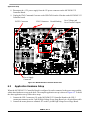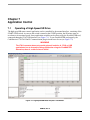
1
DRM100 Designer Reference Manual
Devices Supported:
56F801X
Document Number: DRM100
Rev. 0
06/2008
Contents
Chapter 1
Introduction
1.1 Introduction ............................................................................................................................. 9
1.2 Freescale Digital Signal Controller Advantages and Features ............................................. 10
Chapter 2
SR Motor Control Theory
2.1 Two Phase Switch Reluctance (SR) Motor........................................................................... 13
2.2 Digital Control of an SR Motor .............................................................................................. 15
2.3 Voltage and Current Control of SR Motors ........................................................................... 17
2.3.1 Voltage Control of an SR Motor ................................................................................... 17
2.3.2 Sensorless Position Estimation Using Phase Current Peak Detection ........................ 19
Chapter 3
System Concept
3.1 System Specification............................................................................................................. 21
3.2 Sensorless Drive Concept .................................................................................................... 22
3.3 Control Process .................................................................................................................... 22
3.4 System Blocks Description ................................................................................................... 23
3.4.1 Sensing of Phase Currents and DC-Bus Voltage......................................................... 23
3.4.2 Phase Current Peak Detection..................................................................................... 25
3.4.3 SR Motor Start-Up (Patent No. US6448736 B1) .......................................................... 27
3.4.4 Commutation angle control .......................................................................................... 28
3.4.5 PWM Modulation .......................................................................................................... 29
Chapter 4
Hardware
4.1 Hardware Configuration ........................................................................................................ 31
4.2 MC56F8013/23 Controller Board .......................................................................................... 32
4.3 3-Phase Switched Reluctance High Voltage Power Stage................................................... 33
4.4 2-phase Switched Reluctance Motor .................................................................................... 34
Chapter 5
Software Design
5.1 Introduction ........................................................................................................................... 35
5.2 Main Software Flow Chart..................................................................................................... 35
5.3 Data Flow.............................................................................................................................. 36
5.4 Processes Description .......................................................................................................... 37
5.4.1 Process Current Peak Detection .................................................................................. 37
5.4.2 Process Manual Interface............................................................................................. 37
5.4.3 Process Application State Machine.............................................................................. 38
5.4.4 Process Ramp.............................................................................................................. 38
5.4.5 Process Commutation .................................................................................................. 38
5.4.6 Process PWM Update and DC Bus Voltage Correction............................................... 39
5.5 Fast Interrupts....................................................................................................................... 39
5.5.1 QTimer Ch3 Compare Fast Interrupt............................................................................ 39
5.5.2 QTimer Ch2 Compare Fast Interrupt............................................................................ 39
5.6 Application Variables Scaling................................................................................................ 40
5.6.1 Fractional Numbers Representation............................................................................. 40
5.6.2 Scaling of Analog Quantities ........................................................................................ 40
5.7 Constant Calculation............................................................................................................. 41
5.7.1 Alignment Constants .................................................................................................... 41
5.7.2 Start Up Constants ....................................................................................................... 41
5.7.3 Current Measurement Constants ................................................................................. 42
5.7.4 Voltage Measurement Constants ................................................................................. 43
5.7.5 SR Motor Related Constants........................................................................................ 43
5.8 Software Customizing for another SR Motor ........................................................................ 44
5.9 Real Figures taken by the Oscilloscope................................................................................ 44
Chapter 6
Application Setup
6.1 MC56F8013 Controller Board Setup..................................................................................... 47
6.2 Application Hardware Setup ................................................................................................. 48
6.3 Application Software Setup................................................................................................... 49
6.3.1 Application Software Files ............................................................................................ 49
6.3.2 Application PC Master Software Control Files ............................................................. 50
6.3.3 Application Build........................................................................................................... 50
6.3.4 Programming the MCU................................................................................................. 51
Chapter 7
Application Control
7.1 Operating of High Speed SR Drive ....................................................................................... 53
Appendix A
References
Appendix B
Glossary of Abbreviations
Figures
2-Phase 4/2 SR Motor ................................................................................................................ 13
Aligned/Unaligned Rotor Position of a 2-Phase SR motor.......................................................... 14
Phase Energizing........................................................................................................................ 15
2-Phase SR Power Stage ........................................................................................................... 16
Soft Switching and Hard Switching ............................................................................................. 17
Voltage Control Technique ......................................................................................................... 18
Voltage Control Technique - Voltage and Current Profiles ......................................................... 18
Rotor Position at Phase Current Peak ........................................................................................ 19
System Concept.......................................................................................................................... 23
Phase Current Circuit.................................................................................................................. 24
Phase Current Sampling............................................................................................................. 25
The Current Peak Detection Algorithm ....................................................................................... 26
Start Up Algorithm....................................................................................................................... 27
Commutation angle Control ........................................................................................................ 28
Hardware System Configuration ................................................................................................. 31
MC56F8013/23 Controller Board Top View ................................................................................ 33
3-Phase SR High Voltage Power Stage ..................................................................................... 34
Main Software Flow Chart........................................................................................................... 36
Data flow ..................................................................................................................................... 37
Application State Machine .......................................................................................................... 38
Commutation angles definition.................................................................................................... 44
SR Motor Start Up....................................................................................................................... 45
SR motor operation at low speed (5700 RPM) ........................................................................... 45
SR motor operation at maximal speed (61 000 RPM) ................................................................ 46
MC56F8013/23 Controller Board View ....................................................................................... 48
Demo Application Connection Overview..................................................................................... 49
Execute Make Command............................................................................................................ 50
Execute Debug Command.......................................................................................................... 51
High Speed SR Motor Project in FreeMaster.............................................................................. 53
Setting FreeMASTER Communication ....................................................................................... 54
Tables
Memory Configuration................................................................................................................. 10
PWM Output Setting ................................................................................................................... 29
Electrical Characteristics of 3-Phase SR Power Stage............................................................... 34
QTimer Ch3 Compare Fast Interrupt routines ............................................................................ 39
MC56F8013/23 Controller Board Jumper Setting....................................................................... 47
Chapter 1
Introduction
1.1
Introduction
This designer reference manual describes a sensorless high speed Switch Reluctance (SR) motor drive,
where the rotor position detection is based on phase current peak detection. The presented high speed SR
drive is targeted mainly at vacuum cleaners and other appliance and industry applications, which can
benefit from small motor size and high speed. Usage of the Freescale Semiconductor MC56F8013 device
ensures cost-effective implementation for this type of motor control application.
The switched reluctance motor brings advantages in both cost and reliability over other types of adjustable
speed drives, such as a simple mechanical construction, high efficiency, high power density and so on. On
the other hand, large torque ripple, due to double saliency construction, limits usage of the switch
reluctance motor in many applications. One of the SR motor advantages is operation at high speed
(> 50 000 RPM). It results in a smaller motor for a given output power and reduces the size and weight of
the target application. A typical application which can benefit from this feature, is a vacuum cleaner. The
high speed SR motor makes the vacuum cleaner smaller and lighter, and the noise generated by torque
ripple is comparable with other types of motors.
To run an SR motor properly, the position of the rotor has to be known. The control of an SR motor with
a position sensor is quite tricky and the sensor increases the total system cost and decreases overall
reliability of the drive. Therefore, there is a huge effort to implement control methods for SR motor without
any position sensors. The presented technique is based on phase current peak detection. The phase current
peak corresponds to a certain position of the motor. If this peak is detected, the position of the rotor can be
determined. The phase current peak is evaluated fully by software implemented on the Freescale digital
signal controller MC56F8013 dedicated to various motor control applications. The application described
hereafter covers the following features of the SR motor drive:
• High speed 2-phase SR motor sensorless control based on current peak detection
• Designed to fit vacuum cleaner applications
• Capable of running an SR motor at more than 100 000 RPM (tested with an SR motor designed for
60 000 RPM)
• Single direction of rotation given by asymmetric construction of a 2-phase SR motor
• Speed open loop control
• Start up from any position using alignment and patented algorithm (Patent No. US6448736 B1)
• Start up time and maximal speed depends on the SR motor parameters
DRM100, Rev. 0
Freescale Semiconductor
9
Introduction
1.2
Freescale Digital Signal Controller Advantages and Features
The Freescale MC56F80xx family is well suited to digital motor control, combining the DSP’s calculation
capability with the MCU’s controller features on a single chip. These hybrid controllers offer many
dedicated peripherals such as pulse width modulation (PWM) modules, analog-to-digital converters
(ADC), timers, communication peripherals (SCI, SPI, I2C), and on-board Flash and RAM.
The MC56F80xx family members provide the following peripheral blocks:
• One PWM module with PWM outputs, fault inputs, fault-tolerant design with dead time insertion,
supporting both centre-aligned and edge-aligned modes
• 12-bit ADC, supporting two simultaneous conversions; ADC and PWM modules can be
synchronized
• One dedicated 16-bit general purpose quad timer module
• One serial peripheral interface (SPI)
• One serial communications interface (SCI) with LIN slave functionality
• One inter-integrated circuit (I2C) port
• On-board 3.3V to 2.5V voltage regulator for powering internal logic and memories
• Integrated power-on reset and low voltage interrupt module
• All pins multiplexed with general purpose input/output (GPIO) pins
• Computer operating properly (COP) watchdog timer
• External reset input pin for hardware reset
• JTAG/On-Chip Emulation (OnCE™) module for unobtrusive, processor-speed-independent
debugging
• Phase-locked loop (PLL) based frequency synthesizer for the hybrid controller core clock, with
on-chip relaxation oscillator
Table 1-1. Memory Configuration
Memory Type
MC56F8013
MC56F8023
Program Flash
16 KByte
32 KByte
Unified Data/Program RAM
4 KByte
8 KByte
The two-phase SR control benefits greatly from the flexible PWM module, fast ADC, quad timer module
and interrupt controller module.
The PWM block has the following features:
• Three complementary PWM signal pairs, six independent PWM signals (or a combination)
• Complementary channel operation features
• Independent top and bottom dead time insertion
• Separate top and bottom pulse width correction via current status inputs or software
• Separate top and bottom polarity control
• Edge-aligned or centre-aligned PWM reference signals
• 15-bit resolution
• Half-cycle reload capability
• Integral reload rates from one to sixteen periods
• Mask/swap capability
• Individual, software-controlled PWM output
• Programmable fault protection
DRM100, Rev. 0
10
Freescale Semiconductor
Introduction
•
•
•
Polarity control
10mA or 16mA current sink capability on PWM pins
Write-protectable registers
The PWM offers flexibility in its configuration, enabling efficient two phase SR motor control. The
interesting features of the PWM module (from an SR motor control point of view) are the automatic copy
of duty cycle values to all value registers and the software and masks controls. This automatic copying
simplifies duty cycle control, where a single duty cycle update is necessary to update all PWM channels.
The software control is used to perform unipolar PWM generation (bottom transistor is ON during the
whole period). The last feature - mask control is used for phase commutation or disabling the inactive
phase. The PWM reload SYNC signal is generated to provide synchronization with other modules
(Quadtimers, ADC).
The ADC module has the following features:
• 12-bit resolution
• Dual ADCs per module; three input channels per ADC
• Maximum ADC clock frequency of 5.33MHz with a 187ns period
• Sampling rate of up to 1.78 million samples per second
• Single conversion time of 8.5 ADC clock cycles (8.5 x 187ns = 1.59μs)
• Additional conversion time of six ADC clock cycles (6 x 187ns = 1.125μs)
• Eight conversions in 26.5 ADC clock cycles (26.5 x 187ns = 4.97μs) using parallel mode
• Ability to use the SYNC input signal to synchronize with the PWM (provided the integration
allows the PWM to trigger a timer channel connected to the SYNC input)
• Ability to sequentially scan and store up to eight measurements
• Ability to scan and store up to four measurements on each of two ADCs operating simultaneously
and in parallel
• Ability to scan and store up to four measurements on each of two ADCs operating asynchronously
to each other in parallel
• Interrupt generating capabilities at the end of a scan when an out-of-range limit is exceeded and on
a zero crossing
• Optional sample correction by subtracting a pre-programmed offset value
• Signed or unsigned result
• Single-ended or differential inputs
• PWM outputs with hysteresis for three of the analog inputs
The application uses the ADC block in simultaneous mode scan. It is synchronized to the PWM pulses.
This configuration allows the simultaneous conversion of the DC-bus current and voltage within the
required time.
The quad timer is an extremely flexible module, providing all required services relating to time events. It
has the following features:
• Four 16-bit counters/timers
• Count up/down
• Counters are cascadable
• Programmable count modulus
• Maximum count rate equal to the peripheral clock/2, when counting external events
• Maximum count rate equal to the peripheral clock/1, when using internal clocks
DRM100, Rev. 0
Freescale Semiconductor
11
Introduction
•
•
•
•
•
Count once or repeatedly
Counters are preloadable
Counters can share available input pins
Each counter has a separate prescaler
Each counter has capture and compare capability
The application uses four channels of the quad timer for:
• One channel for PWM-to-ADC synchronization
• One channel for motor commutation
• One channel for system time base (5ms period)
The interrupt controller (ITCN) has the following features:
• Four programmable priority levels for each IRQ
• Two programmable Fast Interrupts
• Notifies the SIM module to restart clocks out of Wait and Stop modes
• Ability to drive the initial address on the address bus after reset
Fast interrupts are used for ADC measurement and motor commutation. This minimizes overhead caused
by frequently calling the interrupt routine. (the ADC sensing interrupt is called every 4.4 μs).
DRM100, Rev. 0
12
Freescale Semiconductor
Chapter 2
SR Motor Control Theory
2.1
Two Phase Switch Reluctance (SR) Motor
A Switched Reluctance (SR) motor is a rotating electric machine where both stator and rotor have salient
poles. The stator winding is comprised of a set of coils, each of which is wound on one pole. The rotor is
created from lamination in order to minimize the eddy-current losses.
SR motors differ in the number of phases wound on the stator. Each of them has a certain number of
suitable combinations of stator and rotor poles. Figure 2-1 illustrates a typical 2-Phase SR motor with a
4/2 (stator/rotor) pole configuration and a stepped gap. The stepped gap is used due to eliminate dead
zones, where motor torque is zero at a symmetrical SR motor and it ensures motor start up in the proper
direction.
Phase B
Stator (4 poles)
Stator
Winding
Phase A
Rotor (2 poles)
Figure 2-1. 2-Phase 4/2 SR Motor
The motor is excited by a sequence of current pulses applied at each phase. The individual phases are
consequently excited, forcing the motor to rotate. The current pulses need to be applied to the respective
phase at the exact rotor position relative to the excited phase. When any pair of rotor poles is exactly in
line with the stator poles of the selected phase, the phase is said to be in an aligned position, i.e., the rotor
DRM100, Rev. 0
Freescale Semiconductor
13
SR Motor Control Theory
is in the position of maximal stator inductance (see Figure 2-2). If the axis of the rotor is in line with
interpolar axis of the stator poles, the rotor is said to be in an unaligned position, i.e., the rotor is in a
position of minimal stator inductance.
Aligned Position
Unaligned Position
Figure 2-2. Aligned/Unaligned Rotor Position of a 2-Phase SR motor
The inductance profile of SR motors is triangular shaped, with maximum inductance when it is in an
aligned position and minimum inductance when unaligned. Figure 2-3 illustrates the idealized
triangular-like inductance profile of both two phases of an SR motor with phase A highlighted. The
individual Phases A and B are shifted electrically by 180o relative to each other. When the respective phase
is powered, the interval is called the dwell angle - θdwell. It is defined by the turn-on θon and the turn-off
θoff angles.
When the voltage is applied to the stator phase, the motor creates torque in the direction of increasing
inductance. When the phase is energized in its minimum inductance position, the rotor moves to the
forthcoming position of maximal inductance. The movement is defined by the magnetization
characteristics of the motor. A typical current profile for a constant phase voltage is shown in Figure 2-3.
For a constant phase voltage the phase current has its maximum in the position when the inductance starts
to increase. This corresponds to the position where the rotor and the stator poles start to overlap. When the
phase is turned off, the phase current falls to zero. The phase current present in the region of decreasing
inductance generates negative torque. The torque generated by the motor is controlled by the applied phase
voltage and by the appropriate definition of switching turn-on and turn-off angles. For more details,
see [12].
As is apparent from the description, the SR motor requires position feedback for motor phase
commutation. In many cases, this requirement is addressed by using position sensors, like encoders, Hall
sensors, etc. The result is that the implementation of mechanical sensors increases costs and decreases
system reliability. Traditionally, developers of motion control products have attempted to lower system
costs by reducing the number of sensors. A variety of algorithms for sensorless control have been
developed, most of which involve evaluation of the variation of magnetic circuit parameters that are
dependent on the rotor position.
DRM100, Rev. 0
14
Freescale Semiconductor
SR Motor Control Theory
Stator Phase A
Aligned
Unaligned
Aligned
Rotor
iphA
LA
LB
position / time
qdwell
Phase A
Energizing
qon _phA
qoff _phA
position / time
Figure 2-3. Phase Energizing
The motor itself is a low cost machine of simple construction. Since high-speed operation is possible, the
motor is suitable for high speed applications, like vacuum cleaners, fans, white goods, etc. As discussed
above, the disadvantage of the SR motor is the need for shaft-position information for the proper switching
of individual phases. Also, the motor structure causes noise and torque ripple. The greater the number of
poles, the smoother the torque ripple, but motor construction and control electronics become more
expensive. Torque ripple can also be reduced by advanced control techniques such as phase current
profiling. The detail mathematical description of the SR motor can be seen in [11].
2.2
Digital Control of an SR Motor
The SR motor is driven by voltage strokes coupled with the given rotor position. The profile of the phase
current together with the magnetization characteristics define the generated torque and thus the speed of
the motor. Due to this fact, the motor requires electronic control for operation. Several power stage
topologies are being implemented, according to the number of motor phases and the desired control
algorithm. The particular structure of the SR power stage structure defines the freedom of control for an
individual phase.
A power stage with two independent power switches per motor phase is the most used topology. Such a
power stage for 3-Phase SR motors is illustrated in Figure 2-4. It enables control of the individual phases
fully independent of each other and thus permits the widest freedom of control. Other power stage
topologies share some of the power devices for several phases, thus saving on power stage cost, but with
these the phases cannot be fully independently controlled. Note that this particular topology of SR power
DRM100, Rev. 0
Freescale Semiconductor
15
SR Motor Control Theory
stage is fault tolerant -- in contrast to power stages of AC induction motors -- because it eliminates the
possibility of a rail-to-rail short circuit.
During normal operation, the electromagnetic flux in an SR motor is not constant and must be built for
every stroke. In the motoring period, these strokes correspond to the rotor position when the rotor poles
are approaching the corresponding stator pole of the excited phase. In the case of Phase A, shown in
Figure 2-1, the stroke can be established by activating the switches Q1 and Q2. At low-speed operation the
Pulse Width Modulation (PWM), applied to the corresponding switches, modulates the voltage level.
Two basic switching techniques can be applied:
•
•
Soft switching - where one transistor is left turned-on during the whole commutation period and
PWM is applied to the other one
Hard switching - where PWM is applied to both transistors simultaneously
DC Voltage
Q1
PWM_Q1
+
D1
Phase A
Q3
PWM_Q3
D1
Phase B
Cap
D2
D2
Q2
PWM_Q2
Q4
PWM_Q4
GND
Figure 2-4. 2-Phase SR Power Stage
Figure 2-5 illustrates both soft and hard switching PWM techniques. The control signals for the upper and
the lower switches of the above-described power stage define the phase voltage and thus the phase current.
The soft switching technique generates lower current ripple compared to the hard switching technique.
Also, it produces lower acoustic noise and less EMI. Therefore, soft switching techniques are often
preferred for motoring operations. For more details, see [12].
DRM100, Rev. 0
16
Freescale Semiconductor
SR Motor Control Theory
Unaligned
Unaligned
Aligned
Aligned
Stator Poles
Rotor Poles
Inductance
PWM
PWM
Upper Switch
PWM
Lower Switch
+VDC
+VDC
Phase Voltage
-VDC
-VDC
Phase Current
Turn On
Turn Off
Position
Soft Switching
Turn On
Turn Off
Position
Hard Switching
Figure 2-5. Soft Switching and Hard Switching
2.3
Voltage and Current Control of SR Motors
A number of control techniques for SR motors exist. They differ in the structure of the control algorithm
and in position evaluation. Two basic techniques for controlling SR motors can be distinguished, according
to the motor variables that are being controlled:
•
•
Voltage control - where phase voltage is a controlled variable
Current control - where phase current is a controlled variable
The next section describes voltage control used in this application. Details about current control can be
found in [11].
2.3.1
Voltage Control of an SR Motor
In voltage control techniques, the voltage applied to the motor phases is constant during the complete
sampling period of the speed control loop. The commutation of the phases is linked to the position of the
rotor.
The voltage applied to the phase is directly controlled by a speed controller. The speed controller processes
the speed error -- the difference between the desired speed and the actual speed -- and generates the desired
DRM100, Rev. 0
Freescale Semiconductor
17
SR Motor Control Theory
phase voltage. The phase voltage is defined by a PWM duty cycle implemented at the DC-Bus voltage of
the SR inverter. The phase voltage is constant during a complete dwell angle. The technique is illustrated
in Figure 2-6. The current and the voltage profiles can be seen in Figure 2-7. The phase current is at its
peak at the position when the inductance starts to increase (stator and rotor poles start to overlap) due to
the change in the inductance profile.
Power Stage
Controller
ωdesired
Σ
-
ωerror
Speed
Controller
PWM Output
Duty Cycle
PWM
Generator
ωactual
θon
θoff
Figure 2-6. Voltage Control Technique
L
iph
θon
UDC-Bus*PWM
θoff
phase current
decays through
the fly back diodes
position / time
uph
PWM = Speed
Controller Output
position / time
-UDC-Bus
Figure 2-7. Voltage Control Technique - Voltage and Current Profiles
DRM100, Rev. 0
18
Freescale Semiconductor
SR Motor Control Theory
2.3.2
Sensorless Position Estimation Using Phase Current Peak Detection
The flux linkage estimation method ranks among the most popular sensorless SR position estimation
techniques. A number of methods that use the flux linkage calculation have been developed in [11, 14, 15].
These methods calculate the actual phase flux linkage and use its relation to the reference flux linkage for
position estimation.
The main disadvantage of all these methods is that the estimation of the flux linkage is based on a precise
knowledge of the phase resistance. The phase resistance varies significantly with temperature which yields
to unwanted integration errors, especially at low speed. These integration errors create a significant
position estimation error.
Another method for sensorless position estimation presented in this reference design manual is based on a
phase current peak detection. The principle of this method can be seen in Figure 2-8. The phase starts to
be excited at the moment corresponding to a desired current amplitude. The current begins to rise till the
position where the stator and rotor poles start to overlap. At this moment, the phase current reaches it’s
maximum. Since we know the exact position of the rotor, we can estimate rotor position based on this
current peak. If the current peak is detected, the peak time is saved. Knowing the time of two consecutive
current peaks, we can calculate the commutation period and corresponding on/off times. The current peak
can be detected by external circuitry, or, nowadays, using powerful digital signal controller, it can be
evaluated directly by software.
Stator Phase A
Aligned
Just in touch
Aligned
Rotor
iphA
LB
LA
position / time
Figure 2-8. Rotor Position at Phase Current Peak
The advantage of this method is that it is independent of the motor parameters. Everything we need to
know is the rotor position at the current peak. Another advantage is that the current peak detection
algorithm is very simple in comparison with estimation of the flux linkage method. It allows to use this
method at very high speed, where the precision of the flux linkage estimation is low due to low number of
current samples for flux calculation. From principle of the operation, this method can be used with voltage
control only since at current control we lose information about the current peak.
The resented SR drive measures the current of the excited phase directly by the integrated analog to digital
converter. Every new current sample is evaluated by the current peak detection algorithm. If the current
peak is detected, the new commutation period is calculated together with on/off times for the next
commutation.
DRM100, Rev. 0
Freescale Semiconductor
19
SR Motor Control Theory
DRM100, Rev. 0
20
Freescale Semiconductor
Chapter 3
System Concept
3.1
System Specification
The system is designed to drive a two-phase SR motor. The application meets the following performance
specification:
• Targeted at the MC56F8013 Controller Board
• Running on a 3-phase SR High Voltage Power Stage (standard Freescale HW platform used)
• Control technique incorporating:
— High speed 2-phase SR motor sensorless control based on a current peak detection
— Direct current sensing by integrated analog to digital converter
— Software current peak evaluation
— Designed to fit vacuum cleaner applications
— Capable of running an SR motor to more than 100 000 RPM (tested with an SR motor designed
for 60 000 RPM)
— Single direction of rotation given by asymmetric construction of 2-phase SR motor
— Speed open loop control
— Start up from any position using alignment and patented algorithm (Patent No. US6448736 B1)
— Start up time and maximal speed depending on the SR motor parameters
DRM100, Rev. 0
Freescale Semiconductor
21
System Concept
3.2
Sensorless Drive Concept
A standard system concept is chosen for the drive (see Figure 3-1). The system incorporates the following
hardware boards:
• 3-phase SR High Voltage Power Stage
• Two Phase SR motor
• MC56F8013/23 Controller Board
NOTE
A two phase SR power stage is required for the two phase SR motor.
However, development of this high speed SR drive was done on a three
phase SR power stage since this power stage is available as a standard
development platform. The third phase on the power stage was unused.
The MC56F8013/23 Controller Board executes the control algorithm. In response to the user interface and
feedback signals, it generates PWM signals for the 3-phase SR High Voltage Power Stage. High-voltage
waveforms generated by the DC to AC inverter are applied to the motor.
3.3
Control Process
The state of the user interface is scanned periodically, while the DC-Bus voltage and the current of the
exciting phase is sampled. The SR motor starts on command from the START/STOP switch. At first the
rotor of the SR motor is aligned to a known position. As soon as the rotor is stabilized, the start up
algorithm begins to excite the phases to get the SR motor running. During the start up, the rotor position
is evaluated by a special patented algorithm (Patent No. US6448736 B1). Once the SR motor achieves a
stable speed, the rotor position is evaluated from the peak current. After the start up sequence, the SR
motor speed is increased by a speed ramp up to a maximal speed.
The DC-Bus voltage and current of the excited phase is sampled with an ADC. The ADC sampling is
triggered by QuadTimer channel 3 and synchronized to the PWM signal.
The current samples are evaluated by the peak detection algorithm. Once the peak is detected the time of
the peak is read and saved for further calculation. After the peak detection, the actual commutation period
and on/off times are calculated from the latest and previous peak times. The DC-Bus voltage is sensed
simultaneously with the phase current and it is used for DC-Bus voltage ripple elimination. DC-Bus
voltage ripple elimination is required for applications where only a small DC-Bus capacitor is used and
variation of the DC-Bus voltage is too large.
The overall state of the application is controlled by an application state machine, which is executed in
a background loop.The application state machine (ASM), consists of init, stop, alignment, start up, run and
error states.
In the case of an overcurrent condition, the signals for the 3-phase inverter are disabled and the fault state
is displayed.
Beyond this, the FreeMASTER interface enables monitoring and adjustment of all system variables.
DRM100, Rev. 0
22
Freescale Semiconductor
System Concept
2-Phase SR Power Stage
Power Line
2-Phase Inverter
DC Bus Voltage & Phase
Current Sensing
VDCB
IPh A
2-Phase
SR Motor
IPh B
ADC Module
Phase
Currents
PWM Module
DC Bus
Voltage
Duty cycle
Current Peak
Detection
DC Bus Voltage
Correction
Commutation
Period
Commutation
Angle Control
Phase
Current
Start/Stop
Speed Up/Down
Other purposes
GPIO
Module
Start Up
Algorithm
Ramp
Generation
Comm.
Sequence
JTAG
Required voltage
On board
Programming/
FreeMASTER
MC56F8013 Controller Board
Figure 3-1. System Concept
3.4
3.4.1
System Blocks Description
Sensing of Phase Currents and DC-Bus Voltage
The control algorithm requires sensing of the following quantities:
• Phase Currents
• DC-Bus voltage
The phase current sensing circuit is shown in Figure 3-2. The phase current is sensed as a voltage drop on
shunt resistor R1. Analyzing the signal on R1, we can find, that the phase current can be seen on shunt
resistor R1 only when both transistors Q1 and Q2 are switched ON. Therefore, the current sampling has
to be synchronized with PWM generation. This can be ensured by PWM to ADC synchronization
implemented on the MC56F8013. This synchronization is performed by the third channel of the quad
timer, where it is connected to the synchronization input of the A/D converter, and the input of the same
channel is connected to the Reload signal of the PWM module. Thus, the quad timer channel 3 allows
control of the delay between the PWM module Reload event and the start of A/D conversion.
DRM100, Rev. 0
Freescale Semiconductor
23
System Concept
Figure 3-2. Phase Current Circuit
Another aspect which has to be considered for the current sampling, is the time resolution for the current
peak detection. At high speeds, the SR motor commutation period is very short. For example, a 2-phase
SR motor with a maximal speed of 60 000 RPM has a commutation period 250 μs only. Since the current
is usually sampled once per PWM period, at a common switching frequency of 16 kHz we get four current
samples only. And this is not enough for current peak evaluation with sufficient time resolution. This issue
can be resolved by implementing multiple current sampling during the PWM period. Actual
implementation can be seen in Figure 3-3. The number of ADC samples taken during a PWM period is
calculated at the beginning of every PWM cycle according to the actual duty cycle (PWM Reload ISR).
The first ADC sample is set to 2 μs after a Reload event. Once the delay elapses, the A/D conversion is
started and a fast interrupt is called (Quad Timer Ch3 ISR). During ADC conversion, quad timer channel 3
is set for a new delay of 4.4 μs when the next current sample is taken. The first delay of 2 μs is set due to
the propagation delay caused by the IGBT driver and on time of the IGBT transistor. The delay between
other samples is set to 4.4 μs. Since at a maximal speed the duty cycle is 100%, the current is sampled
continuously every 4.4 μs.
DRM100, Rev. 0
24
Freescale Semiconductor
System Concept
PWM Period
Phase
Current
PWM
Reload
ISR
Quad Timer
Compare1
ISR
Current
Sample
2ms
4.4ms
2ms - due to propagation delay
4.4ms - Phase Current Sampling Period
Quad
Timer
Ch3
Output
ADC Trigger
Signal
PWM
Output
Current Sampling not possible
when PWM OFF
Figure 3-3. Phase Current Sampling
This method allows detecting the current peak with a time precision better than 2%. The current sampling
starts at the beginning of each commutation and stops when the current peak is detected. Besides the
current value, the time of each current sample is saved for further commutation calculation. The time base
is derived from Quad Timer Ch2.
The DC-Bus voltage is sampled simultaneously with the phase current, since the MC56F8013 is capable
of converting two samples at the same time. The DC-Bus voltage is used to compensate the DC-Bus
voltage ripple when a small DC Bus capacitor is used.
3.4.2
Phase Current Peak Detection
The phase current peak defines the known position of the rotor. Therefore the current peak detection is the
most important part of the control algorithm. At a glance, to find the maximum from the current samples
seems to be simple. This assumption is true when the motor is running with full voltage. In that case, the
current has a smooth shape and looking for the maximum is simple. The situation becomes more
complicated when PWM modulation is used to control applied voltage on the SR motor, because the
current shape is distorted by PWM modulation. The distortion depends on phase inductance, the type of
the PWM modulation and the PWM switching frequency. Usually, the inductance of the SR motor can not
be easily changed. Therefore the type of PWM modulation and PWM switching frequency are key
parameters in minimizing current distortion. As can be see in Figure 2-5, the unipolar switching is
preferred, due to lower current ripple.
DRM100, Rev. 0
Freescale Semiconductor
25
System Concept
actualSample = new sample
First sample
in PWM period?
YES
lastFirstSample = firstSample
firstSample = actualSample
NO
Last sample
in PWM period?
YES
LastSample = actualSample
NO
New
maximum?
YES
peakCurrent =actualSample
peakTime = actualTime
NO
YES
peakCurrent
>
lastFirstSample
NO
YES
lastFirstSample
>
FirstSample
NO
YES
FirstSample
>
actualSample
NO
PEAK DETECTED
NO PEAK DETECTED
Figure 3-4. The Current Peak Detection Algorithm
The minimal acceptable PWM switching frequency depends mainly on the phase inductance of the SR
motor. In the presented application, 16kHz seems to be a good compromise between current ripple and
switching losses.
DRM100, Rev. 0
26
Freescale Semiconductor
System Concept
Due to current ripple, the peak detection algorithm is more complex. Apart from the actual and maximal
currents, the first and last current samples are also consider for peak evaluation. The final implementation
of the current peak detection algorithm can be seen in Figure 3-4. Based on experience with several SR
motors, the current peak detection algorithm may require a little adaptation (adding a hysteresis) to reflect
specific parameters of the SR motor used. The hysteresis is also used for peak and minimum detection
during start up. The algorithm is executed on every new available current sample.
3.4.3
SR Motor Start-Up (Patent No. US6448736 B1)
The presented sensorless algorithm does not allow detecting rotor position from a zero speed. Therefore,
to start the SR motor, two issues have to be solved:
• The initial position of the rotor is unknown when the SR motor starts up
• The commutation times are calculated from the actual period, which is zero at the start
The first issue can be resolved very easily by rotor alignment. During alignment, the one phase is excited
for a certain time and the rotor is pulled into an aligned position (see Figure 2-5). The alignment time
depends on motor inertia and it can be even a few seconds for larger motors.
If the rotor is aligned, the motor is ready for start up. The rotor starts to move when the next phase is
excited. The right direction of rotation is ensured by asymmetric rotor construction. Once the rotor starts
to move, the speed of the rotor is unknown so the current peak is not sufficient for the next commutation
calculation. Therefore, a different algorithm has been developed to ensure proper start up.
Stator Phase A
Aligned
Just in touch
Rotor
Aligned position passed
Current Peak
iphA
LB
Next
Commutation
LA
Current Minimum
position / time
Figure 3-5. Start Up Algorithm
The start up algorithm consist of two parts. The first part is the same as during a run state. The algorithm
detects the peak of the phase current. If the rotor continues from a “touch” position to the alignment
position, the phase current drops down. As soon as the rotor passes the aligned position, the phase current
starts to rise again (see Figure 3-5). And this moment is the right time for commutation. Put Another way,
if the current peak is detected, the algorithm starts to look for the current minimum. Once the phase current
minimum is cached, the commutation is immediately performed. After several commutations (4-8
commutations) executed based on the start up algorithm, the rotor speed is stabilized and the commutation
DRM100, Rev. 0
Freescale Semiconductor
27
System Concept
period can be calculated. If the commutation period is known, the sensorless algorithm can be switched to
current peak detection only.
The advantage of this start up algorithm is with motor parameters and load independency. So it ensures a
reliable start up in a wide range of start conditions. This algorithm was patented by Freescale as Patent No.
US6448736 B1.
3.4.4
Commutation angle control
Based on the known actual period and rotor angle at current peak, the TON and TOFF times can be
calculated for the next commutation:
θ OFF – θ PEAK⎞
t OFF = t PEAK + T C ⋅ ⎛ -------------------------------⎝
⎠
90°
(EQ 3-1)
90° – θ PEAK + θ ON
t ON = t PEAK + T C ⋅ ⎛ -------------------------------------------⎞
⎝
⎠
90°
(EQ 3-2)
where:
tOFF
tON
tPEAK
TC
θOFF
θPEAK
off time of excited phase
on time of next phase switch on
time of actual current peak
actual commutation period
off angle of excited period
angle (rotor position) at current peak
TC
iPhB
qON
qPEAK
TON TPEAK
iPhA
qOFF
TOFF TON TPEAK
TOFF
position / time
Figure 3-6. Commutation angle Control
During start up, the SR motor speed is controlled by PWM only and θON and θOFF remains constant. Once
the SR motor is supplied by full voltage, the angle control is used to control the motor speed. The θON and
θOFF are usually changed in such a way that the difference θOFF - θON is kept constant.
DRM100, Rev. 0
28
Freescale Semiconductor
System Concept
3.4.4.1
DC-Bus Voltage Correction
If a small DC-Bus capacitor is used, the DC-Bus voltage varies with mains frequency. If the DC-Bus
voltage variation is too high there is an impact on phase current recognition. Therefore the DC-Bus voltage
correction algorithm is used to keep the phase voltage as constant as possible.
3.4.5
PWM Modulation
The PWM module implemented on the MC56F80xx has very good support for an SR motor control. To
run an SR motor, four independent PWM signals are necessary. Since the unipolar switching is used to
minimize current ripple both the bottom transistors are switched on over the whole PWM period.
Therefore these two outputs are set under software control, with output set to 1. This allows using another
interesting feature - value register acceleration. This feature, if enabled, copies the value written in value
register 0 to all other value registers. This allows setting the duty cycle for both phases (top transistors)
with a single write to value register. The last feature, masking, is used for motor commutation. It enables
PWM outputs of a particular phase based on actual rotor positions. A summary of PWM settings for all
PWM outputs can be seen in Table 3-1. The PWM period is restarted at the beginning of a commutation
period to keep the same voltage condition for each commutation period.
Table 3-1. PWM Output Setting
PWM Channel
SW Control
Mask Control
0
Disabled
used based on rotor position
1
Enabled (Set to 1)
used based on rotor position
2
Disabled
used based on rotor position
3
Enabled (Set to 1)
used based on rotor position
DRM100, Rev. 0
Freescale Semiconductor
29
System Concept
DRM100, Rev. 0
30
Freescale Semiconductor
Chapter 4
Hardware
4.1
Hardware Configuration
The application is designed to drive a high speed 2-phase SR motor. It consists of the following modules:
• Host PC
• MC56F8013/23 Controller Board
• 3-phase SR High Voltage Power Stage (just 2 phases utilized)
• 2-phase SR Motor
MC56F8013
Controller Board
J4
40 pin
flat
cable
J1
3-phase HV SR motor
Power Stage
J14
The application hardware system configuration is shown in Figure 4-1.
J11
1
2
~230V/50Hz
14 pin
flat
cable
JTAG/
USB
Conv.
J13
PhC PhB PhA
PC
CodeWarrior
FreeMaster
SR
Motor
Figure 4-1. Hardware System Configuration
All system parts are documented in these references:
• MC56F8013/23 Controller Board:
— Using Freescale’s MC56F8013 or MC56F8023 as the controller
— Described in the MC56F8013/23 Controller Board User’s Manual
• 3-Phase Switched Reluctance High Voltage Power Stage:
— High-voltage three-phase power stage with single-phase input 115/230 Volt AC and 750
VoltAmp.
— Described in the 3-Phase Switched Reluctance High Voltage Power Stage User’s Manual
A detailed description of each individual board can be found in the appropriate user manual, or on the
Freescale web site http://www.freescale.com. The user manuals include a schematic of the board, a
description of individual function blocks, and a bill of materials (parts list).
DRM100, Rev. 0
Freescale Semiconductor
31
Hardware
4.2
MC56F8013/23 Controller Board
The MC56F8013/23 controller board is based on an optimized PCB and power supply design. It
demonstrates the abilities of the MC56F8013/23 and provides a hardware tool to help in the development
of applications using the MC56F8013/23 targeted at motor control applications.
The MC56F8013/23 Controller Board can be populated either by MC56F8013 or MC56F8023 parts. PCBs
marked with the numbers 00216A01 and 00216A02 are populated by an MC56F8013 device. PCBs
marked with the numbers 00216B02 are populated by an MC56F8023 device.
The controller board is an evaluation module type of board; it includes an MC56F8013 or MC56F8023
part, encoder interface, tacho-generator interface, communication options, digital and analog power
supplies, and peripheral expansion connectors. The expansion connectors are for signal monitoring and
user feature expandability. Test pads are provided for monitoring critical signals and voltage levels.
The MC56F8013/23 controller board is designed for the following purposes:
• To allow new users to become familiar with the features of the MC56F801x/802x architecture.
• To serve as a platform for real-time software development. The tool suite allows you to develop
and simulate routines, download the software to on-chip memory, run the software, and debug it
using a debugger via the JTAG/OnCETM port. The breakpoint features of the OnCE port let you
specify complex break conditions easily and execute your software at full-speed, until the break
conditions are satisfied. The ability to examine and modify all user accessible registers, memory,
and peripherals through the OnCE port simplifies considerably the task of the developer.
• To serve as a platform for hardware development. The hardware platform enables external
hardware modules to be connected. The OnCE port's unobtrusive design means all of the memory
on the digital signal controller chip is available to the user.
The board facilitates the evaluation of various features present in the MC56F8013/8023,and can be used
to develop real-time software and hardware products based on the MC56F8013 or the MC56F8023. It
provides the features necessary to write and debug software, demonstrate the functionality of that software,
and to interface with the customer's application specific device(s). The MC56F8013/23 Controller Board
is flexible enough to allow full exploitation of the MC56F8013/8023's features to optimize the
performance of the user’s end product. See Figure 4-2.
DRM100, Rev. 0
32
Freescale Semiconductor
Hardware
Figure 4-2. MC56F8013/23 Controller Board Top View
4.3
3-Phase Switched Reluctance High Voltage Power Stage
Freescale’s three-phase high-voltage (HV) SR power stage is an up to 750-voltamps (one horsepower),
3-phase power stage that will operate off DC input voltages from 140 to 325 volts, and AC line voltages
from 100 to 240 volts. In combination with one of the controller boards, it provides a software
development platform that allows algorithms to be written and tested without the need to design and build
a power stage. It supports a wide variety of algorithms for SR motors. The presented application utilizes
just two phases.
The high-voltage SR power stage has a printed circuit board and an aluminium backplate. The discrete
devices (an input rectifier, brake IGBT and diode, bridge IGBT’s,) are mounted on the aluminium
backplate, which provides necessary isolation and hence a heatsink can be easily mounted. If possible the
aluminium backplate can be used as a heatsink too.The printed circuit board, situated above the aluminium
backplate, contains IGBT gate drive circuits, analog signal conditioning, low-voltage power supplies, and
some large, passive, power components (see Figure 4-3).
Input connections are made via the 40-pin ribbon cable connector J14. Power connections to the motor are
made on output connector J13. Phase A, phase B, and phase C are labelled Ph_A, Ph_B, and Ph_C on the
board. Power requirements are met by a single external 140 to 325 volt DC power supply or an AC line
voltage. Either input is supplied through connector J11. An external brake resistor can be connected via
connector J12. Current measuring circuitry is set up for +/-20 amps full scale. Both bus and phase leg
currents are measured.
DRM100, Rev. 0
Freescale Semiconductor
33
Hardware
Figure 4-3. 3-Phase SR High Voltage Power Stage
Table 4-1. Electrical Characteristics of 3-Phase SR Power Stage
Characteristic
Symbol
Min
Typ
Max
Units
DC input voltage
Vdc
140
—
325
V
AC input voltage
Vac
100
—
240
V
Logic 1 Input Voltage
VIH
2.0
—
—
V
Logic 0 Input Voltage
VIL
—
—
0.8
V
Analog Output Range
VOut
0
—
3.3
V
Bus Current Sense Voltage
ISense
—
82.5
—
mV/A
Bus Current Sense Offset
Ioffset
Bus Voltage Sense Voltage
VBus
Bus Voltage Sense Offset
Voffset
4.4
+VREF
—
8.09
0
V
—
mV/V
V
2-phase Switched Reluctance Motor
The application drives a high speed SR motor. Since it is hard to find suitable high speed switch reluctance
motors on the market, the custom SR motor was used for development. The nominal speed of this SR
motor is 60 000 RPM. Other parameters are confidential, therefore, no more details will be mentioned in
this reference design manual.
DRM100, Rev. 0
34
Freescale Semiconductor
Chapter 5
Software Design
5.1
Introduction
This section describes the design of the drive’s software blocks. The software description comprises these
topics:
• Main Software Flow Chart
• Data Flow
5.2
Main Software Flow Chart
The main software flow chart incorporates the main routine (background loop) entered from reset, and the
interrupt events. The main routine includes the initialization of the microcontroller and the main loop.
After initialization, the main routine enters an endless loop which executes the application state machine
consisting of init, stop, alignment, start up, run and error states. The transition between the states depends
on the state of the START/ STOP switch and drive status. The main software flow chart is given in
Figure 5-1. Apart from the background loop, the software incorporates the following four interrupts:
• QTimer Channel 1 Compare Interrupt
Interrupt Level: 0
Execution Period: 5 ms
The interrupt routine performs software timing for the application. This time base is used for ramps
generation, handling of the user interface.
• PWM Reload Interrupt
Interrupt Level: 1
Execution Period: 62.5 μs
The interrupt routine performs DC Bus voltage correction and calculates the number of phase
current samples taken, based on the actual duty cycle.
• QTimer Channel 3 Compare Interrupt
Interrupt Level: 2
Execution Period: 4.4 μs
The interrupt routine evaluates the phase current samples and detects the current peak. If the
current peak is detected, the commutation period and the next commutation event are calculated.
• QTimer Channel 2 Compare Interrupt
Interrupt Level: 2
Execution Period: Driven by event
The interrupt routine performs the commutation.
DRM100, Rev. 0
Freescale Semiconductor
35
Software Design
QTimer Ch1 Compare
(5 ms)
Main (background) loop
- Ramp generation
- User interface handling
INFINITE LOOP
Initialize
- Peripheral initialization
- Application initialization
Application State Machine
- Init state
- Stop state
- Alignment state
- Start up state
- Run state
- Error state
QTimer Ch2 Compare
(driven by event)
- Commutation
QTimer Ch3 Compare
(4.4 ms)
- Peak detection
- Period calculation
- Next commutation
- calculation
PWM Reload
(62.5 ms)
- DC Bus voltage correction
- Number of current samples
- calculation
Figure 5-1. Main Software Flow Chart
5.3
Data Flow
The High Speed Sensorless SR drive control algorithm is described in the data flow chart shown in
Figure 5-2. The variables actualCurrent and dcbVoltage contain results of ADC conversion. The Current
peak detection process evaluates actualCurrent together with auxiliary variables peakCurrent,
minCurrent, firstCurrentSample, lastFirstCurrentSample, lastCurrentSample. If the peak current is
detected, the time of the peak is saved into peakTime and commutationPeriod is calculated. Once the
current peak is detected, the new commutation events OnTime and OffTime are calculated using the known
commutation period and the onAngle, offAngle and peakAngle variables.The values of OnTime and
OffTime, shown in italic, are not declared as variable but are written directly to the QTimer Ch2 Compare
and Preload registers.
The actual state of the user interface is monitored by the Manual Interface Process and is saved in the
interfaceStatus variable. Based on this state, and other state variables not mentioned in the main data flow
chart (adcProcessingState), the Application State Machine sets its state AppState.
Actual motor speed is defined by pwmDutyCycle. This command is passed through the Ramp Process
(pwmDutyCycleRamp), and after DC Bus voltage correction, is written into PWM module.
DRM100, Rev. 0
36
Freescale Semiconductor
Software Design
onAngle
offAngle
peakAngle
actualCurrent
Manual Interface
Process
Current Peak
Detection
interfaceStatus
peakTime
Application State
Machine
appState
OnTime
OffTime
commutationPeriod
Commutation
Process
pwmDutyCycle
dcbVoltage
Ramp
Process
DC Bus voltage
Correction
pwmDutyCycleRamp
pwmDutyCycleCorrected
PWM
Update
Figure 5-2. Data flow
5.4
Processes Description
The main processes of the high speed sensorless SR drive application can be also seen in Figure 5-2.
5.4.1
Process Current Peak Detection
This process is called in the QTimer Ch3 Compare interrupt. The process evaluates the actual current
samples and detects a current minimum and peak. The detection algorithm differs according to the drive
state. In alignment state, the current samples are not evaluated. In start up state, both the current minimums
and peaks are detected for the start up algorithm. Once the drive switches to run state, the only current peak
is needed for SR motor operation. The details about current evaluation can be seen in Section 3.3 Control
Process.
5.4.2
Process Manual Interface
This process checks the state of the input pin where the START/STOP switch is connected. If a change is
detected, the particular status bit is set. These status bits are evaluated in the Application State Machine.
The process is executed every 5 ms in the QTimer Ch1 Compare interrupt.
DRM100, Rev. 0
Freescale Semiconductor
37
Software Design
5.4.3
Process Application State Machine
The application state machine (ASM), consists of init, stop, alignment, start up, run and error states (see
Figure 5-3). After an MCU reset, the ASM goes through the init state to the stop state. As soon as the user
turns the START/STOP switch to the START position, the ASM goes into the alignment state, where the
motor is aligned to a known position. After a predefined time the ASM continues to the start up state. At
the start up state, the rotor position is evaluated by the start up algorithm based on minimum and peak
current detection. After eight proper commutations, the ASM goes into the run state and SR motor speed
is increased linearly up to the maximal speed. In the case of any fault, the ASM goes into the error state
and then into the stop state. The ASM is executed in the background loop.
CPU RESET
INIT
STOP
Alignment
Start up
ERROR
RUN
Figure 5-3. Application State Machine
5.4.4
Process Ramp
T aim of this process is to keep the slope of the duty cycle change within the desired range. This process
is executed in the QTimer Ch1 Compare interrupt, like the Manual Interface Process.
5.4.5
Process Commutation
The process commutation can be divided into two parts. The first part is executed once the current peak is
detected. The process calculates the new commutation period and the next commutation events (off time
for the actually excited phase, on time for the next phase). This part is executed in the QTimer Ch3
Compare interrupt. The second part provides commutation (disables/enables the appropriate phase). It is
executed in the QTimer Ch2 Compare interrupt.
DRM100, Rev. 0
38
Freescale Semiconductor
Software Design
5.4.6
Process PWM Update and DC Bus Voltage Correction
The PWM module is updated by the actual duty cycle, which is corrected for DC Bus voltage variation.
Both the DC Bus voltage correction and duty cycle update are executed in the PWM Reload interrupt. The
PWM output masking (enabling/disabling) phase is done asynchronously by the commutation process.
5.5
Fast Interrupts
Fast interrupts are used to execute the current peak detection algorithm and commutation. The advantage
of a fast interrupt is minimal interrupt latency and a simple change of interrupt service routine since the
interrupt vector is located in a dedicated register. It allows switching the called routine with minimal
overhead.
5.5.1
QTimer Ch3 Compare Fast Interrupt
This interrupt routine performs current sample evaluation. Since the evaluation algorithm depends on the
state of the SR drive, the different service routines are called based on the actual application state.
Table 5-1 shows which service routine is called for each state of the application state machine. All routines
are written is assembler to get maximal performance. The execution period of this interrupt is 4.4 μs if
more than one sample taken during the PWM period.
Table 5-1. QTimer Ch3 Compare Fast Interrupt routines
5.5.2
Application State
QTimer Ch3 Compare Fast Interrupt
Alignment
IsrAdcAlignment
Start Up
IsrAdcStart
Run
IsrAdcRun
QTimer Ch2 Compare Fast Interrupt
Also, this fast interrupt calls two different service routines:
1. IsrQT2DisablePhase routine
2. IsrQT2SwapPhase routine
Once the current peak is detected, the execution times are preloaded into Compare 1 and Compare Load 1
registers and the QTimer Ch2 Fast Interrupt is set to call the IsrQT2DisablePhase routine. As soon as the
event happens, the IsrQT2DisablePhase routine disables the excited phase and the interrupt vector is
updated to call the IsrQT2SwapPhase routine. Consequently, the value in the Compare Load 1 register is
moved into the Compare register 1. This update is done automatically by hardware. Now the QTimer is
ready for the next compare event. As soon as the new compare event happens, the IsrQT2SwapPhase
routine is called and the next phase is switched on. So the commutation sequence is completed.
DRM100, Rev. 0
Freescale Semiconductor
39
Software Design
5.6
5.6.1
Application Variables Scaling
Fractional Numbers Representation
The AC induction motor vector control application uses a fractional representation for all real quantities,
except time. The N-bit signed fractional format is represented using 1.[N-1] format (1 sign bit, N-1
fractional bits). Signed fractional numbers (SF) lie in the following range:
– 1.0 ≤ SF ≤ +1.0 -2
–[ N – 1 ]
(EQ 5-3)
For words and long-word signed fractions, the most negative number that can be represented is -1.0, whose
internal representation is $8000 and $80000000, respectively. The most positive word is $7FFF or 1.0 2-15, and the most positive long-word is $7FFFFFFF or 1.0 - 2-31
5.6.2
Scaling of Analog Quantities
Analog quantities such as voltage, current and frequency are scaled to the maximum measurable range,
which is dependent on the hardware. The following equation shows the relationship between a real and a
fractional representation:
Real Value
Fractional Value = -------------------------------------------------Real Quantity Range
where:
Fractional Value
Real Value
Real Quantity Range
RPM,
(EQ 5-4)
is a fractional representation of the real value [Frac16]
is the real value of the quantity [V, A, RPM, etc.]
is the maximum range of the quantity, defined in the application [V, A,
etc.]
The above scaling can be demonstrated on a DC-Bus voltage and motor phase voltage as an example. All
variables representing voltage are scaled to the same scale in the application. They are scaled to maximum
measurable voltage range of the power stage. For the demo hardware board the range is VMAX= 407 V.
Variable values in fractional format are defined by the following equation:
V MEASURED
( Frac16 )voltage_variable= -------------------------------V MAX
(EQ 5-5)
The fractional variables are internally stored as signed 16-bit integer values, whose values can be evaluated
as follows:
( Int16 )voltage_variable = ( Frac16 )voltage_variable ⋅ 2
15
(EQ 5-6)
DRM100, Rev. 0
40
Freescale Semiconductor
Software Design
5.7
5.7.1
Constant Calculation
Alignment Constants
#define ALIGNMENT_RAMP_TIME
700
// in ms
This constant defines ramp aligned time, when the applied voltage on the SR motor during alignment rises
from ALIGNMENT_START_VOLTAGE to ALIGNMENT_VOLTAGE. The constant is defined in ms.
#define ALIGNMENT_STAB_TIME
500
// in ms
This constant defines the time, when the constant voltage ALIGNMENT_VOLTAGE is applied on the SR
motor during alignment. This follows after ALIGNMENT_RAMP_TIME. So the total duration of
alignment is ALIGNMENT_RAMP_TIME + ALIGNMENT_STAB_TIME. The constant is defined in
ms.
#define ALIGNMENT_VOLTAGE
2.5
// as % of DC bus voltage
This constant defines final alignment voltage (kept on the motor during ALIGNMENT_STAB_TIME).
The constant is defined in % of DC Bus voltage.
#define ALIGNMENT_START_VOLTAGE
30
// as % of alignment voltage
This constant defines initial alignment voltage applied on the SR motor at the beginning of alignment. This
constant is defined as a % of ALIGNMENT_VOLTAGE! In this example, it is 30% of 2.5% = 0.75% of
DC Bus voltage.
5.7.2
Start Up Constants
#define START_VOLTAGE
820
// 2.5 % of DC bus voltage =
2.5/100*32768
This constant defines initial start up voltage applied on the SR motor at start up. This value is defined
directly as a fractional value, since it is used in assembler code.
#define START_TIME
3000
// in ms
This constant defines acceleration time, when the SR motor is accelerated from a minimal (start) speed up
to the maximal speed. This time does not include alignment and start up time. The constant is defined in
ms.
#define NUMBER_OF_IGNORED_PEAKS
4
This constant defines the number of commutations, when the start up algorithm is used, to determine a
commutation event.
DRM100, Rev. 0
Freescale Semiconductor
41
Software Design
5.7.3
Current Measurement Constants
#define CURRENT_SCALE
40.0
// in Amps
This constant defines current scale for the power stage. Please note, that CURRENT_SCALE corresponds
to the full range of the ADC converter input voltage (0-3.3V). For motor phase-current sensing, the zero
current level is shifted into the middle of this range (=1.65V). Thus, the maximum positive and negative
phase-current which can be sensed is CURRENT_SCALE/2. In other words, the current sensing range of
the power stage is from -20.0 Amps to + 20.0 Amps. The constant is defined in Amps.
#define CURRENT_HYSTERESIS_START
0.2
// in Amps
This constant defines current hysteresis used for minimum and peak current detection during the start up.
The constant is defined in Amps.
#define CURRENT_HYSTERESIS_START_F16
163
// FRAC16(CURRENT_HYSTERESIS_START/CURRENT_SCALE)
The same variable as above, defined in fractional.
#define FIRST_CURRENT_SAMPLE_DELAY
40
// 1.25 us (32MHz*1.25us)
This constant defines the delay between the beginning of a PWM pulse and the first current samples. It
takes into account the delay of the IGBT drive and measurement path. The constant is defined as an integer
value.
#define CURRENT_SAMPLE_DELAY
141
// 4.4 us (32MHz*4.4us)
This constant defines the delay between current samples, if more than one sample is taken. The constant
is defined as an integer value.
#define DUTY_CYCLE_TO_SAMPLES
FRAC16(((1.0*(PWM_MODULO-CURRENT_SAMPLE_DELAY)/CURRENT_SAMPLE_DELAY))/
(1.0*(PWM_MODULO-FIRST_CURRENT_SAMPLE_DELAY)))
This constant is used for calculating the number of current samples, which can be taken for the actual duty
cycle.
#define NUMBER_OF_ADC_SAMPLES
((PWM_MODULO-CURRENT_SAMPLE_DELAY)/CURRENT_SAMPLE_DELAY) - 1
This constant defines the maximal number of current samples which can be taken for a given switching
frequency and the delay between current samples.
DRM100, Rev. 0
42
Freescale Semiconductor
Software Design
5.7.4
Voltage Measurement Constants
#define DCB_VOLTAGE_SCALE
407.0 //V
This constant defines voltage scale for the power stage. The constant is defined in Volts.
.
#define DCB_VOLTAGE_NOMINAL
325.0 //V
This constant defines nominal DC Bus voltage for 230V mains voltage. The constant is defined in Volts.
5.7.5
SR Motor Related Constants
#define ANGLE_SCALE
90.0 //el. degrees
This constant defines the angle scale for the power stage. The constant is defined in degrees.
#define ON_ANGLE
0.0 //el. degrees
This constant defines the rotor position where the phase starts to be excited. The constant is defined in
degrees.
#define PEAK_ANGLE
35.0 //el. degrees
This constant defines the rotor position where the phase current achieved its peak. The constant is defined
in degrees.
#define OFF_ANGLE
62.0 //el. degrees
This constant defines the rotor position where the excited phase is switched off. The constant is defined in
degrees.
The definition of all angles mentioned above can be seen in Figure 5-4. The figure shows an idealized
relation of inductance on the rotor position.
DRM100, Rev. 0
Freescale Semiconductor
43
Software Design
iphA
LA
LB
ON_ANGLE
0°
PEAK_ANGLE
OFF_ANGLE
90°
Rotor angle [°]
Figure 5-4. Commutation angles definition
5.8
Software Customizing for another SR Motor
The advantage of this algorithm (current peak detection) is that it is not heavily dependent on the motor
parameters. So customizing this software to another motor is quite simple. The process of customizing is
described in following steps:
1. check current and voltage scales on your hardware
2. set the motor constant (Section 5.7.5 SR Motor Related Constants) according to your motor
characteristic.
3. tune the alignment (constants in Section 5.7.1 Alignment Constants) to get reliable alignment. The
constant depends on winding resistance (the voltage constants) and motor inertia (time constants).
4. tune the start up of the motor (constants in Section 5.7.2 Start Up Constants)
5.9
Real Figures taken by the Oscilloscope
The next three figures shows real signals taken by an oscilloscope during development. For all figures
• the yellow color represents the DC Bus voltage,
• magenta and green colors represents phase currents.
The first figure, Figure 5-5, depicts the start up of the SR drive. All phases of the start up sequence can be
observed from this figure. The constant current represents the rotor alignment. The next four pulses show
the operation of the start up algorithm. Both current minimum and peak detections can be observed. After
the fourth pulse, the algorithm uses the current peak to determine the correct position.
The next two figures, Figure 5-6 and Figure 5-7, show motor operations at low (approx. 5700 RPM) and
maximal (approx. 61 000 RPM) speeds.
DRM100, Rev. 0
44
Freescale Semiconductor
Software Design
Figure 5-5. SR Motor Start Up
Figure 5-6. SR motor operation at low speed (5700 RPM)
DRM100, Rev. 0
Freescale Semiconductor
45
Software Design
Figure 5-7. SR motor operation at maximal speed (61 000 RPM)
DRM100, Rev. 0
46
Freescale Semiconductor
Chapter 6
Application Setup
As described earlier, the high speed sensorless SR motor control application is targeted at the MC56F8013
and MC56F8023 devices. The concept of the SR motor vector control drive incorporates the following
hardware components:
• MC56F8013/23 Controller Board
• 3ph SR High Voltage Power Stage Board
• Two-Phase SR Motor
6.1
MC56F8013 Controller Board Setup
Prior to the MC56F8013/23 Controller Board being connected to the power-stage, it needs to be
configured for the correct operation. Also, the demo application code has to be programmed into the Flash
memory first. For the MC56F8013/23 Controller Board configuration follow these steps:
1. Set the jumper configuration on the MC56F8013/23 Controller Board as shown in the table:
Table 6-1. MC56F8013/23 Controller Board Jumper Setting
Jumper
Setting
Description
JP4
1-2, 4-5, 7-8
ADC CFG2 Configuration (motor phase-current sensing)
JP5
1-2, 4-5, 7-8
ADC CFG1 Configuration (motor phase-current sensing)
JP8
1-2
Start switch enabled
JP10
1-2
User LED enabled
J16
1-2
+5V Power Supply from UNI-3 connector
J18
1-2
+15V Power Supply from UNI-3 connector
Note: Other Jumpers are set to OPEN
2. Connect a +12V power supply to the J12 power connector on the MC56F8013/23 Controller
Board.
3. Set the Over-Current/Over-Voltage Thresholds.
4. Trimpot R29 sets the over-voltage threshold. Use a voltmeter to measure the threshold level at
test-point TP3. Turn the R29 trimpot to set the threshold level. Voltage level on TP3 should be
>3.2V.
5. Trimpot R32 sets the over-current threshold. Use a voltmeter to measure the threshold level at
test-point TP5. Turn the R32 trimpot to set the threshold level. Voltage level on TP3 should be
>3.2V.
6. Connect the parallel JTAG Command Converter or the USB-TAP to the host PC and to the J4
header on the MC56F8013/23 Controller board.
7. Compile your project and program it into the device.
DRM100, Rev. 0
Freescale Semiconductor
47
Application Setup
8. Disconnect the +12V power supply from the J12 power connector on the MC56F8013/23
Controller Board.
9. Unplug the JTAG Command Converter or the USB-TAP from the J4 header on the MC56F8013/23
Controller board.
RS232 Connector
UNI-3 Connector
Board Marking
Over-Voltage and
Over-Current Trimpots
Power Supply
Connector
Figure 6-1. MC56F8013/23 Controller Board View
6.2
Application Hardware Setup
When the MC56F8013/23 Controller Board is configured it can be connected to the power stage and the
whole demo hardware set-up can be built. The complete application set-up is shown in Figure 6-2. To build
the demo application set-up follow these steps:
1. Connect the UNI-3 connector (J1) on the MC56F8013/23 Controller Board to the UNI-3
counterpart connector on the 3-ph SR High Voltage Power Stage Board via a 40-pin ribbon cable.
2. Connect the motor phases to terminals J13 on the 3-ph SR High Voltage Power Stage Board.
DRM100, Rev. 0
48
Freescale Semiconductor
Application Setup
40 pin
flat
cable
MC56F8013
Controller Board
J4
J14
3-phase HV SR motor
Power Stage
J1
3. Connect a 230V AC power supply through an isolation transformer or an isolated 325 V DC power
supply to terminals J11 on the 3-ph SR High Voltage Power Stage Board.
J11
1
2
~230V/50Hz
14 pin
flat
cable
JTAG/
USB
Conv.
J13
PhC PhB PhA
PC
CodeWarrior
FreeMaster
SR
Motor
Figure 6-2. Demo Application Connection Overview
4. Switch-on the high-voltage power supply.
5. Start the FreeMASTER project and switch to the control page pane.
WARNING
There is a risk of electric shock! Both the MC56F8013/23 Controller Board
and the 3-ph SR High Voltage Power Stage Board are connected to high
voltage. The galvanic isolation transformer must be used to operate
application by the START/STOP toggle switch.
WARNING
The JTAG connector does not provide galvanic isolation. The demo
hardware set-up has to be disconnected from high-voltage if a JTAG
connection is required. To debug the application, or to download code to the
device flash memory using JTAG, use a low voltage +12V power supply
connected to the J12 connector on the MC56F8013/23 Controller Board!
Another option is to use a JTAG or USB optoisolator for downloading the
application code, or to use the FreeMASTER application.
6.3
6.3.1
Application Software Setup
Application Software Files
The application software files are:
• ...\software\2phase_SRM.mcp, application project file
• ...\software\sources\main.c, main program
• ...\software\sources\main.h, header file for main code
• ...\software\ApplicationConfig\appconfig.h, header file with peripherals initialization. This file
is generated automatically by the configuration tool in the Quick_Start development environment.
DRM100, Rev. 0
Freescale Semiconductor
49
Application Setup
NOTE
Even if the software can be compiled without the Quick_Start development environment,
it is recommended to install the latest version of this tool. It allows comfortable reading and
modification of the appconfig.h file.
6.3.2
Application PC Master Software Control Files
The application FreeMaster software control files are:
• ...\software\Freemaster\BLDC_BEMF_DEMO_S08AW60.pmp, FreeMaster software project file
• ...\software\Freemaster\source, directory with FreeMaster software control page files
6.3.3
Application Build
To build the sensorless BLDC demo application, open the 2phase_SRM.mcp project file and execute the
Make command, as shown in Figure 6-3. This will build and link the application with all the required
Metrowerks libraries.
Figure 6-3. Execute Make Command
DRM100, Rev. 0
50
Freescale Semiconductor
Application Setup
6.3.4
Programming the MCU
To download the software into the microcontroller, use an USB/PARALLEL to JTAG converter. Before
downloading new software, stop the motor by the START/STOP switch and execute the Debug command
as shown in Figure 6-4.
Figure 6-4. Execute Debug Command
CAUTION
The JTAG connector does not provide galvanic isolation. The application
hardware set-up has to be disconnected from high-voltage if a JTAG
connection is required. To debug the application, or to download code to the
device flash memory using JTAG, use a low voltage +12V power supply
connected to the J12 connector on the MC56F8013/23 Controller Board!
Another option is to use a JTAG or USB optoisolator for downloading the
application code, or to use the FreeMASTER application.
DRM100, Rev. 0
Freescale Semiconductor
51
Application Setup
DRM100, Rev. 0
52
Freescale Semiconductor
Chapter 7
Application Control
7.1
Operating of High Speed SR Drive
The high speed SR motor control application can be controlled by the manual interface, consisting of the
START/STOP switch. As soon as the switch is turned to the START position, the SR motor starts to
accelerate to its maximal speed. Some application variables can be observed by the FreeMASTER tool,
connected through a JTAG/USB interface (see Figure 7-1). To run FreeMASTER tool properly, the
CodeWarrior-CCS JTAG/OnCE Communication plug-in mode has to be set (see Figure 7-2)
WARNING
The JTAG connector does not provide galvanic isolation. A JTAG or USB
optoisolator has to be used to debug application using the FreeMASTER.
Otherwise, there is a risk of electric shock!
Figure 7-1. High Speed SR Motor Project in FreeMaster
DRM100, Rev. 0
Freescale Semiconductor
53
Application Control
Figure 7-2. Setting FreeMASTER Communication
DRM100, Rev. 0
54
Freescale Semiconductor
Appendix A
References
The following documents can be found on the Freescale web site: http://www.freescale.com.
1.
2.
3.
4.
5.
6.
7.
8.
9.
10.
11.
12.
13.
14.
15.
16.
56F8013 Data Sheet, MC56F8013, Freescale Semiconductor, 2006
56F8023 Data Sheet, MC56F8023, Freescale Semiconductor, 2006
56F802X and 56F803X Peripheral Reference Manual, MC56F80XXRM, Freescale Semiconductor, 2006
56F801X Peripheral Reference Manual, MC56F8000RM, Freescale Semiconductor, 2006
DSP56800E Reference Manual, DSP56800ERM, Freescale Semiconductor, 2005
CodeWarrior™ Development Studio for Freescale™ 56800/E Digital Signal Controllers, Freescale
Semiconductor, 2006
MC56F8013/23 Controller Board Users Manual, Freescale Semiconductor, 2007
Embedded Motion Control 3-Phase Switched Reluctance High-Voltage Power Stage User's Manual,
Motorola Semiconductor, 2000
Free Master Software Users Manual, Freescale Semiconductor, 2004
Balazovic P., 3-Phase Switched Reluctance motor Control with Encoder Using 56F805, DRM031, Freescale
2003.
Visinka R., Musil J., 3-Phase SR Motor Sensorless Control Reference Design, DRM030, Freescale 2003.
Miller T.J.E., Switched Reluctance Motors and their Control, Magna physics publishing and Clarendon
press, Oxford, 1993.
Gallegos-Lopez, G., A New Sensorless Low-Cost Method for Switched Reluctance Motor Drives,
University of Glasgow - SPEED Laboratory, 1997
Lyons, J.P., MacMinn, S.R., Preston, Flux/Current Methods for SRM Rotor Position Estimation, Proc.
IEEE-IAS’91, 1991
Lajsner P., Visinka R., Vecera I., Method for controlling switched reluctance motor, and controller, Patent
No. US6448736 B1, Motorola 2002
DRM100, Rev. 0.1
Freescale Semiconductor
55
References
DRM100, Rev. 0.1
56
Freescale Semiconductor
Appendix B
Glossary of Abbreviations
AC — alternating current
ADC — analog-to-digital converter
COP — computer operating properly (watchdog timer
DC — direct current
DC/DC Inverter— power electronics module that converts DC voltage level to a different DC voltage
level
DSC — digital signal controller
DT — dead time: a short time that must be inserted between the turning off of one transistor in the inverter
half bridge and turning on of the complementary transistor due to the limited switching speed of the
transistors
duty cycle — the ratio of the amount of time the signal is on to the time it is off. Duty cycle is usually
quoted as a percentage
GPIO — general purpose input/output
interrupt — a temporary break in the sequential execution of a program to respond to signals from
peripheral devices by executing a subroutine
I/O — input/output interfaces between a computer system and the external world. A CPU reads an input
to sense the level of an external signal and writes to an output to change the level of an external signal
JTAG — Joint Test Action Group: acronym commonly used to refer to an interface allowing on-chip
emulation and programming
LED — light emitting diode
MC56F80xx — a Freescale family of 16-bit DSPs dedicated to motor control
PLL — phase-locked loop: a clock generator circuit in which a voltage controlled oscillator produces an
oscillation that is synchronized to a reference signal
PWM — pulse width modulation
Quad timer — a module with four 16-bit timers
reset — to force a device to a known condition
RPM — revolutions per minute
SCI — serial communication interface module: a module that supports asynchronous communication
software — instructions and data that control the operation of a microcontroller
SR — Switched reluctance
DRM100, Rev. 0.1
Freescale Semiconductor
57
Glossary of Abbreviations
DRM100, Rev. 0.1
58
Freescale Semiconductor
How to Reach Us:
Home Page:
www.freescale.com
Web Support:
http://www.freescale.com/support
USA/Europe or Locations Not Listed:
Freescale Semiconductor, Inc.
Technical Information Center, EL516
2100 East Elliot Road
Tempe, Arizona 85284
1-800-521-6274 or +1-480-768-2130
www.freescale.com/support
Europe, Middle East, and Africa:
Freescale Halbleiter Deutschland GmbH
Technical Information Center
Schatzbogen 7
81829 Muenchen, Germany
+44 1296 380 456 (English)
+46 8 52200080 (English)
+49 89 92103 559 (German)
+33 1 69 35 48 48 (French)
www.freescale.com/support
Japan:
Freescale Semiconductor Japan Ltd.
Headquarters
ARCO Tower 15F
1-8-1, Shimo-Meguro, Meguro-ku,
Tokyo 153-0064
Japan
0120 191014 or +81 3 5437 9125
[email protected]
Asia/Pacific:
Freescale Semiconductor China Ltd.
Exchange Building 23F
No. 118 Jianguo Road
Chaoyang District
Beijing 100022
China
+86 10 5879 8000
[email protected]
For Literature Requests Only:
Freescale Semiconductor Literature Distribution Center
P.O. Box 5405
Denver, Colorado 80217
1-800-441-2447 or +1-303-675-2140
Fax: +1-303-675-2150
[email protected]
Information in this document is provided solely to enable system and
software implementers to use Freescale Semiconductor products. There are
no express or implied copyright licenses granted hereunder to design or
fabricate any integrated circuits or integrated circuits based on the
information in this document.
Freescale Semiconductor reserves the right to make changes without further
notice to any products herein. Freescale Semiconductor makes no warranty,
representation or guarantee regarding the suitability of its products for any
particular purpose, nor does Freescale Semiconductor assume any liability
arising out of the application or use of any product or circuit, and specifically
disclaims any and all liability, including without limitation consequential or
incidental damages. “Typical” parameters that may be provided in Freescale
Semiconductor data sheets and/or specifications can and do vary in different
applications and actual performance may vary over time. All operating
parameters, including “Typicals”, must be validated for each customer
application by customer’s technical experts. Freescale Semiconductor does
not convey any license under its patent rights nor the rights of others.
Freescale Semiconductor products are not designed, intended, or authorized
for use as components in systems intended for surgical implant into the body,
or other applications intended to support or sustain life, or for any other
application in which the failure of the Freescale Semiconductor product could
create a situation where personal injury or death may occur. Should Buyer
purchase or use Freescale Semiconductor products for any such unintended
or unauthorized application, Buyer shall indemnify and hold Freescale
Semiconductor and its officers, employees, subsidiaries, affiliates, and
distributors harmless against all claims, costs, damages, and expenses, and
reasonable attorney fees arising out of, directly or indirectly, any claim of
personal injury or death associated with such unintended or unauthorized
use, even if such claim alleges that Freescale Semiconductor was negligent
regarding the design or manufacture of the part.
Freescale™ and the Freescale logo are trademarks of Freescale
Semiconductor, Inc. All other product or service names are the property of their
respective owners.
© Freescale Semiconductor, Inc. 2008. All rights reserved.
DRM100
Rev. 0
06/2008