1
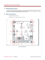
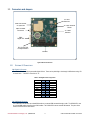
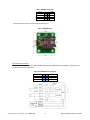
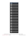
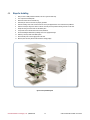
COM16155ER/COM16155RER GSM/GPRS Modem and GPS PCI/104 Module User’s Manual BDM-610020119 Rev. C RTD Embedded Technologies, Inc. AS9100 and ISO 9001 Certified RTD Embedded Technologies, Inc. 103 Innovation Boulevard State College, PA 16803 USA Telephone: 814-234-8087 Fax: 814-234-5218 www.rtd.com [email protected] [email protected] Revision History Rev A Rev B Rev C Initial Release Corrected description of Triorail Module as Tri-Band instead of Quad-Band Corrected SIM-Card Reader section title Fixed default factory settings of GPS and GSM Base Address Jumpers in Table 7 Advanced Analog I/O, Advanced Digital I/O, aAIO, aDIO, a2DIO, Autonomous SmartCal, “Catch the Express”, cpuModule, dspFramework, dspModule, expressMate, ExpressPlatform, HiDANplus, “MIL Value for COTS prices”, multiPort, PlatformBus, and PC/104EZ are trademarks, and “Accessing the Analog World”, dataModule, IDAN, HiDAN, RTD, and the RTD logo are registered trademarks of RTD Embedded Technologies, Inc (formerly Real Time Devices, Inc.). PS/2 is a trademark of International Business Machines Inc. PCI, PCI Express, and PCIe are trademarks of PCI-SIG. PC/104, PC/104-Plus, PCI-104, PCIe/104, PCI/104-Express and 104 are trademarks of the PC/104 Embedded Consortium. All other trademarks appearing in this document are the property of their respective owners. Failure to follow the instructions found in this manual may result in damage to the product described in this manual, or other components of the system. The procedure set forth in this manual shall only be performed by persons qualified to service electronic equipment. Contents and specifications within this manual are given without warranty, and are subject to change without notice. RTD Embedded Technologies, Inc. shall not be liable for errors or omissions in this manual, or for any loss, damage, or injury in connection with the use of this manual. Copyright © 2015 by RTD Embedded Technologies, Inc. All rights reserved. RTD Embedded Technologies, Inc. | www.rtd.com iii COM16155ER/COM16155RER User’s Manual Table of Contents 1 2 3 4 Introduction 7 1.1 Product Overview........................................................................................................................................................................ 7 1.2 Board Features ........................................................................................................................................................................... 7 1.3 Ordering Information ................................................................................................................................................................... 8 1.4 Contact Information .................................................................................................................................................................... 8 1.4.1 Sales Support 8 1.4.2 Technical Support 8 Specifications 9 2.1 Operating Conditions .................................................................................................................................................................. 9 2.2 Electrical Characteristics ............................................................................................................................................................ 9 Board Connection 10 3.1 Board Handling Precautions ..................................................................................................................................................... 10 3.2 Physical Characteristics ............................................................................................................................................................ 10 3.3 Connectors and Jumpers .......................................................................................................................................................... 11 3.3.1 External I/O Connectors 11 CN8: Digital I/O Connector 11 CN6: SIM Module/Connector 11 CN7: GSM Headset Connector 12 3.3.2 Jumpers 13 JP6 & JP7: Base Address Jumpers 13 JP3: GPS Interrupt Jumper 15 3.3.3 Solder Blob Jumpers 15 3.3.4 LED Indicators 15 D1 – SIM card Power 15 D3 – 1 PPS 16 D4 – GSM STATUS Signal 16 3.4 Steps for Installing .................................................................................................................................................................... 17 IDAN Connections 18 4.1 Module Handling Precautions ................................................................................................................................................... 18 4.2 Physical Characteristics ............................................................................................................................................................ 18 4.3 Connectors................................................................................................................................................................................ 18 4.3.1 External I/O Connectors 18 Digital I/O Connector 18 Headset Connector 19 4.4 Steps for Installing .................................................................................................................................................................... 20 5 Functional Description 5.1.1 Cinterion MC55i-W Quad-Band Cellular Engine (COM16155ER) MC55i-W Module Interface GSM Antenna Considerations SIM-Card Reader 5.1.2 Linx RXM-GNSS-TM GPS Receiver GPS module interface GPS Antenna 5.1.3 Digital I/O 21 21 22 22 22 22 23 23 23 6 Register Address Space 24 6.1 General Board Control .............................................................................................................................................................. 24 6.1.1 UART I/O (GPS/GSM BASE + 0 to GPS/GSM BASE + 7) 25 6.1.2 GSM Status (GSM BASE +402h) 25 6.1.3 GSM Control (GSM BASE +403h) 25 6.1.4 GPS Status (GPS BASE + 401h) 25 RTD Embedded Technologies, Inc. | www.rtd.com iv COM16155ER/COM16155RER User’s Manual 6.1.5 6.1.6 7 9 26 26 6.2 COM17045 Compatibility .......................................................................................................................................................... 27 6.3 Using the GSM Engine ............................................................................................................................................................. 27 6.3.1 Starting up and logging into the GSM network 27 6.3.2 Using SMS 27 Troubleshooting 7.1 8 Digital I/O RTD ISA ID 28 Common Problems and Solutions ............................................................................................................................................ 28 Additional Information 29 8.1 PC/104 Specifications ............................................................................................................................................................... 29 8.2 Linx RXM-GNSS-TM ................................................................................................................................................................ 29 8.3 Cinterion MC55i Cellular Engine............................................................................................................................................... 29 Limited Warranty RTD Embedded Technologies, Inc. | www.rtd.com 30 v COM16155ER/COM16155RER User’s Manual Table of Figures Figure 1: Board Dimensions ................................................................................................................................................................................... 10 Figure 2: Board Connections .................................................................................................................................................................................. 11 Figure 3: ESIM2035 Board ..................................................................................................................................................................................... 12 Figure 4: Example 104™Stack ............................................................................................................................................................................... 17 Figure 5: IDAN Dimensions .................................................................................................................................................................................... 18 Figure 6: Example IDAN System ............................................................................................................................................................................ 20 Figure 7: COM16155 Block Diagram ...................................................................................................................................................................... 21 Table of Tables Table 1: Ordering Options ........................................................................................................................................................................................ 8 Table 2: Operating Conditions .................................................................................................................................................................................. 9 Table 3: Electrical Characteristics ............................................................................................................................................................................ 9 Table 4: CN7 Digital I/O Pin Assignments .............................................................................................................................................................. 11 Table 5: CN6 SIM Pin Assignment ......................................................................................................................................................................... 12 Table 6: CN7 GSM Headset Pin Assignment ......................................................................................................................................................... 12 Table 7: Jumper Settings ........................................................................................................................................................................................ 13 Table 8: IDAN- COM16155 25-Pin Subminiature "D" Connector ........................................................................................................................... 19 Table 9: IDAN- COM16155 9-Pin Subminiature "D" Connector ............................................................................................................................. 19 Table 10: Received Signal Strength Values ........................................................................................................................................................... 22 Table 11: Register Map .......................................................................................................................................................................................... 24 Table 12: Register Map .......................................................................................................................................................................................... 24 Table 13: GSM STATUS (GSM BASE + 402h) ...................................................................................................................................................... 25 Table 14: GSM Control (GSM BASE + 403h)......................................................................................................................................................... 25 Table 15: GPS STATUS (GPS BASE + 401h) ....................................................................................................................................................... 25 Table 16: Digital I/O Data (GPS/GSM BASE + 404h) ............................................................................................................................................ 26 Table 17: Digital I/O Data (GPS/GSM BASE + 405h) ............................................................................................................................................ 26 Table 18: Digital I/O Direction (GPS/GSM BASE + 406h) ...................................................................................................................................... 26 Table 19: Digital I/O Direction (GPS/GSM BASE + 407h) ...................................................................................................................................... 26 Table 20: RTD ID DATA READ Indexes................................................................................................................................................................. 26 Table 21: Digital I/O Data (GPS BASE + 400h)...................................................................................................................................................... 27 Table 22: Digital I/O Data (GPS BASE + 400h)...................................................................................................................................................... 27 Table 23: Troubleshooting ...................................................................................................................................................................................... 28 RTD Embedded Technologies, Inc. | www.rtd.com vi COM16155ER/COM16155RER User’s Manual 1 Introduction 1.1 Product Overview The COM16155 is designed to provide quad-band GSM and GPRS with global positioning system (GPS) for PCI/104 based systems. Included on the COM16155 are a Cinterion MC55i-W quad band GSM cellular modem and a Linx RXM-GNSS-TM GPS Receiver module. The COM16155 has an ISA UART chip that permits communication with serial port on the GSM as well as the serial port on the GPS receiver module over the PCI/104 bus without using other serial ports in the PC/104 system. The GSM module supports an enhanced AT command set and the GPS supports National Marine Electronics Association (NMEA-0183 ver. 4.10) messages. The COM16155R uses the Triorail Tri-band GSM cellular modem instead of the Cinterion MC55i-W for railroad applications. 1.2 Board Features Direct connections to the GSM module GSM module o GSM 850/900/1800/1900 MHz (COM16155) o o o o o GSM-R 900/1800/1900 MHz (COM16155R) GPRS Multislot Class 10 o o o o o o o o L1 1575.42MHz, C/A code 33-channel satellite tracking AT command set SMS Fax Linx RXM-GNSS-TM GPS engine Position accuracy: 2.5m Time accuracy of ±11ns 1Hz update rate (configurable up to 10Hz) Tracking sensitivity down to -164 dBm Protocol: NMEA-0183 ver 4.10 Constellation System Support: o (RTCM) Radio Technical Commission for Maritime Services (WAAS) Wide-Area Augmentation System (EGNOS) European Geo-Stationary Navigation System (MSAS) MTSAT Satellite-Based Augmentation System (GAGAN) GPS-Aided Geo-Augmented Navigation Standard 16C550 UART Interface o o o o GALILEO QZSS DGPS support: (SBAS) Satellite-Based Augmentation System GPS GLONASS Compatible with all modern operating systems. Jumper-selectable Base Address and IRQ Optional 1 PPS on carrier-detect TX and RX only, no flow control or handshaking required Digital I/O o 16 bit-programmable Digital I/O RTD Embedded Technologies, Inc. | www.rtd.com 7 COM16155ER/COM16155RER User’s Manual o Optional 1PPS on DIO0 PCI/104 compliant 1.3 Ordering Information The COM16155 is available in the following options: Table 1: Ordering Options Part Number COM16155ER-1 COM16155ER-2 COM16155RER-1 COM16155RER-2 IDAN-COM16155ERS IDAN-COM16155RERS Note: Description PC/104 Cellular Modem Module (on-board SIM-card reader) PCI/104 Cellular Modem Module (external SIM-card reader) PC/104 Cellular Modem Module (on-board SIM-card reader) PCI/104 Cellular Modem Module (external SIM-card reader) PC/104 Cellular Modem IDAN Module PC/104 Cellular Modem IDAN Module Throughout this document, COM16155 refers to both the COM16155 and COM16155R unless otherwise noted The Intelligent Data Acquisition Node (IDAN™) building block can be used in just about any combination with other IDAN building blocks to create a simple but rugged 104™ stack. This module can also be incorporated in a custom-built RTD HiDAN™ or HiDANplus High Reliability Intelligent Data Acquisition Node. Contact RTD sales for more information on our high reliability systems. 1.4 Contact Information 1.4.1 SALES SUPPORT For sales inquiries, you can contact RTD Embedded Technologies sales via the following methods: Phone: E-Mail: 1.4.2 1-814-234-8087 [email protected] Monday through Friday, 8:00am to 5:00pm (EST). TECHNICAL SUPPORT If you are having problems with you system, please try the steps in the Troubleshooting section of this manual. For help with this product, or any other product made by RTD, you can contact RTD Embedded Technologies technical support via the following methods: Phone: E-Mail: 1-814-234-8087 Monday through Friday, 8:00am to 5:00pm (EST). [email protected] RTD Embedded Technologies, Inc. | www.rtd.com 8 COM16155ER/COM16155RER User’s Manual 2 Specifications 2.1 Operating Conditions Table 2: Operating Conditions Symbol Vcc5 Vcc3 Vcc12 Ta Ts RH Parameter 5V Supply Voltage 3.3V Supply Voltage 12V Supply Voltage Operating Temperature Storage Temperature Relative Humidity MTBF Mean Time Before Failure Test Condition Non-Condensing Telcordia Issue 2 30°C, Ground benign, controlled Min 4.75 n/a n/a -30 -40 0 Max 5.25 n/a n/a +70 +85 90% TBD Unit V V V C C % Hours 2.2 Electrical Characteristics Table 3: Electrical Characteristics Symbol P Icc Parameter Power Consumption 5V Input Supply Current VIH VIL VOH VOL Input High Voltage Input Low Voltage Output High Voltage Output Low Voltage 5V Output Pull-up/Pull-down RTD Embedded Technologies, Inc. | www.rtd.com Test Condition Vcc5 = 5.0V Active Digital I/O CN7 CN7 IO = -4mA CN7 IO = 8mA CN7 CN7 9 Min 2.0 -0 2.4 0 Typ TBD TBD Max Unit W mA 5.5 0.8 3.3 0.4 200 10K V V V V mA Ω COM16155ER/COM16155RER User’s Manual 3 Board Connection 3.1 Board Handling Precautions To prevent damage due to Electrostatic Discharge (ESD), keep your board in its antistatic bag until you are ready to install it into your system. When removing it from the bag, hold the board at the edges, and do not touch the components or connectors. Handle the board in an antistatic environment, and use a grounded workbench for testing and handling of your hardware. 3.2 Physical Characteristics Weight: Approximately 80 g (0.18 lbs.) Dimensions: 90.17 mm L x 95.89 mm W (3.550 in L x 3.775 in W) Figure 1: Board Dimensions RTD Embedded Technologies, Inc. | www.rtd.com 10 COM16155ER/COM16155RER User’s Manual 3.3 Connectors and Jumpers J3: GPS Antenna SIM Card socket or connector CN4 CN5: Headset Connector J5: GPS Antenna Power J2: GSM Antenna Connector CN8: Digital I/O JP4 & JP5: DIO Pullup/Pulldown ISA Bus Figure 2: Board Connections 3.3.1 EXTERNAL I/O CONNECTORS CN8: Digital I/O Connector The COM16155 offers 16 bit-programmable digital I/O lines. These can be pulled high or low through 10KΩ resistors using JP4 to control bits 0 – 7 and JP5 to control bits 8 – 15 Table 4: CN7 Digital I/O Pin Assignments DIO0 DIO2 DIO4 DIO6 +5V DIO8 DIO10 DIO12 DIO14 +5V 2 4 6 8 10 12 14 16 18 20 1 3 5 7 9 11 13 15 17 19 GND DIO1 DIO3 DIO5 DIO7 GND DIO9 DIO11 DIO13 DIO15 CN6: SIM Module/Connector The COM16155 can use either an onboard SIM module or an external SIM connected through a cable. The COM16155-1 uses an on-board SIM module and will not have CN4 installed. The COM16155-2 uses an external SIM module. The pinout of the external connector CN6 is shown below. RTD Embedded Technologies, Inc. | www.rtd.com 11 COM16155ER/COM16155RER User’s Manual Table 5: CN6 SIM Pin Assignment Vcc GND GND Card Detect GND 2 4 6 8 10 1 3 5 7 9 GND Reset I/O CLK Vcc The figure below shows a picture of the external SIM card interface board. Figure 3: ESIM2035 Board CN7: GSM Headset Connector The COM16155 Headset connector is used to connect a headset to the GSM module for voice operation. The pin-out of the external connector CN5 is shown below. Table 6: CN7 GSM Headset Pin Assignment MICP EPP VMICP Reserved GND RTD Embedded Technologies, Inc. | www.rtd.com 2 4 6 8 10 1 3 5 7 9 12 GND MICN EPN VMICN Reserved COM16155ER/COM16155RER User’s Manual 3.3.2 JUMPERS The following sections describe the jumper configuration options available on the COM16155. The default factory jumper settings are listed in the following table: Table 7: Jumper Settings Jumper JP1 Description GPS Active Antenna Power JP2 JP3 JP4 GSM Interrupt Jumper GSP Interrupt Jumper Pull-up or Pull-down for DIO0-7 JP5 Pull-up or Pull-down for DIO8-15 JP6 JP7 JP8 GPS Base Address Jumper GSM Base Address Jumper COM16155/COM17045 Mode JP9 1PPS on UART carrier detect (COM16155 mode only) Jumper Settings 1-2: +5.0V 2-3: +3.3V Open for passive antennas Set GSM Interrupt Set GPS Interrupt 1-2: Pull-up 2-3: Pull-down No connect – Neither 1-2: Pull-up 2-3: Pull-down No connect – Neither Sets GPS Address Sets GSM Address 1-2: COM17045 Compatible 2-3: COM16155 1-2: Enables 1PPS on UART CD 2-3: Disable 1PPS on UART CD Default Factory Setting 1-2 5 and G 11 and G 2-3 2-3 3E8 2E8 2-3 2-3 JP6 & JP7: Base Address Jumpers The base address selection jumpers (A3 through A8) allow you to set the base address of the first UART that connects to the GPS module and the second UART that connects to the GSM module. Any software that accesses the board will do so through reads and writes to the I/O address set by the jumpers. To function properly, the I/O address the software is expecting must match the base address set by the jumpers. As shown in the figure below, A3 is located at the left end of the jumper block, while A8 is located at the right end: The table on the following pages shows the possible base address settings for the COM16155. All base addresses are in hexadecimal. An ‘X’ indicates a closed jumper, while an empty cell indicates an open jumper. Base Address (Hexadecimal) A8 A7 200 208 210 218 220 228 230 238 240 248 250 RTD Embedded Technologies, Inc. | www.rtd.com Jumpers A6 A5 A4 A3 X X X X X X X X X X 13 X X X X X X X COM16155ER/COM16155RER User’s Manual Base Address (Hexadecimal) 258 260 268 270 278 280 288 290 298 2A0 2A8 2B0 2B8 2C0 2C8 2D0 2D8 2E0 2E8 2F0 2F8 300 308 310 318 320 328 330 338 340 348 350 358 360 368 370 378 380 388 390 398 3A0 3A8 3B0 3B8 3C0 3C8 3D0 3D8 3E0 3E8 3F0 3F8 A8 A7 Jumpers A6 A5 X X X X X X X X X X X X X X X X X X X X X X X X X X X X X X X X X X X X X X X X X X X X X X X X X X X X X X X X X A4 A3 X X X X X X X X X X X X X X X X X X X X X X X X X X X X X X X X X X X X X X X X X X X X X X X X X X X X X X X X X X X X X X X X X X X X X X X X X X X X X X X X X X X X X X X X X X X X X X X X X X X X X X X X X X X X X X X X X X X X X X By default, the COM16155 comes configured with a base address of 0x3E8 for the GPS UART and 0x2E8 for the GSM UART. RTD Embedded Technologies, Inc. | www.rtd.com 14 COM16155ER/COM16155RER User’s Manual When selecting a base address for the COM16155, please observe the following guidelines: Every device in your PC/104 system must have a unique base address! When selecting a base address for the COM16155, make certain that it does not conflict with any other devices. Base addresses 0x3F8 and 0x2F8 are typically used by serial ports COM1 and COM2, respectively. If you wish to use one of those base addresses, you will need to disable any conflicting serial port. Some operating systems expect UART devices to be located at the standard serial port base addresses (0x3F8, 0x2F8, 0x3E8, and 0x2E8). Setting your COM16155 to one of these addresses can make system setup and configuration easier. JP3: GPS Interrupt Jumper The IRQ selection jumpers allow you to set the IRQ used by the serial port UART of the COM16155. The COM16155 can be configured for any one of the following IRQs: 2, 5, 6, 7, 10, 11, 12, 14, or 15. The IRQ can be set by closing the appropriately labeled jumper on the board. The UART’s carrier detect signal, which is driven by the GPS 1 PPS, can be an interrupt source. Default GSM Setting: IRQ 5 and G Jumper closed Default GPS Setting: IRQ 11 and G Jumper closed Note: Typically IRQs cannot be shared; although there are some special cases (see “The G Jumper” later in this document). In general, the IRQ you select should not be used by any other devices in your system. Reserved IRQs Some of the IRQ choices on the COM16155 may already be used by your CPU’s onboard peripherals. Some commonly-used IRQs are: IRQ 2/9 is used by some VGA controllers. IRQ 5 or 7 may be used by the CPU’s parallel port. Check your CPU’s configuration to avoid a conflict. IRQ 12 is used by the PS/2 mouse. To use this IRQ, you will need to remove the PS/2 mouse from the system. Some CPUs also require a BIOS setting to disable the PS/2 mouse controller. IRQ 14 is used by the primary IDE controller. To use this IRQ, you will need to disable the primary IDE controller. IRQ 15 is used by the secondary IDE controller. To use this IRQ, you will need to disable the secondary IDE controller. The G Jumper The COM16155 supports shared interrupts as defined by the PC/104 specification. This sharing is accomplished via the G jumper, which is located adjacent to the IRQ jumpers. The G jumper installs a 1KΩ resistor to pull the signal to the low state, allowing an interrupt to drive the signal high. To share interrupts, configure the devices for the same IRQ, then close the G jumper on one (and only one) of the devices. When using interrupt sharing, consider the following guidelines: An interrupt can only be shared if all devices on the IRQ support it. If you have two sharing and one non-sharing device on the same IRQ, it will not work. To share interrupts, the system’s drivers and operating system must support it. The Interrupt Service routines must be written to check all devices on an IRQ when the interrupt is detected. Many popular operating systems do not support interrupt sharing for ISA devices. Note: 3.3.3 If you are not sharing interrupts, make sure you leave the COM16155’s G jumper closed! SOLDER BLOB JUMPERS All solder blob jumpers are reserved for factory use and should not be changed. 3.3.4 LED INDICATORS D1 – SIM card Power RTD Embedded Technologies, Inc. | www.rtd.com 15 COM16155ER/COM16155RER User’s Manual On when the SIM card is being powered from the cellular module D3 – 1 PPS Provides 1 PPS to LED, begins to flash once GPS has satellite fix. D4 – GSM STATUS Signal The GSM AT^SSYNC command serves to configure the STATUS pin of the application interface. The pin can either be used to indicate the current consumption in a transmit burst (default setting) or to drive a status LED connected to the pin. See the AT^SSYNC command for details. RTD Embedded Technologies, Inc. | www.rtd.com 16 COM16155ER/COM16155RER User’s Manual 3.4 Steps for Installing 1. 2. 3. 4. 5. 6. 7. 8. 9. 10. 11. 12. Always work at an ESD protected workstation, and wear a grounded wrist-strap. Turn off power to the PC/104 system or stack. Select and install stand-offs to properly position the module on the stack. Remove the module from its anti-static bag. Check that pins of the bus connector are properly positioned. Check the stacking order; make sure all of the busses used by the peripheral cards are connected to the cpuModule. Hold the module by its edges and orient it so the bus connector pins line up with the matching connector on the stack. Gently and evenly press the module onto the PC/104 stack. If any boards are to be stacked above this module, install them. Attach any necessary cables to the PC/104 stack. Re-connect the power cord and apply power to the stack. Boot the system and verify that all of the hardware is working properly. NOTE: When using under Windows, the GPS may be incorrectly detected as a Serial Mouse, causing erratic mouse cursor behavior. This issue has been documented by Microsoft. For more information, refer to Microsoft Knowledge Base Article 283063. Figure 4: Example 104™Stack RTD Embedded Technologies, Inc. | www.rtd.com 17 COM16155ER/COM16155RER User’s Manual 4 IDAN Connections 4.1 Module Handling Precautions To prevent damage due to Electrostatic Discharge (ESD), keep your module in its antistatic bag until you are ready to install it into your system. When removing it from the bag, hold the module by the aluminum enclosure, and do not touch the components or connectors. Handle the module in an antistatic environment, and use a grounded workbench for testing and handling of your hardware. 4.2 Physical Characteristics Weight: Approximately 0.21 Kg (0.46 lbs.) Dimensions: 151.972 mm L x 129.978 mm W x 16.993 mm H (5.983 in L x 5.117 in W x 0.669 in H) Figure 5: IDAN Dimensions 4.3 Connectors 4.3.1 EXTERNAL I/O CONNECTORS Digital I/O Connector RTD Embedded Technologies, Inc. | www.rtd.com 18 COM16155ER/COM16155RER User’s Manual Connector Part #: Amp 747913-2 Sample Mating Connector: Amp 3-1740199-2 Table 8: IDAN- COM16155 25-Pin Subminiature "D" Connector IDAN Pin# 1 2 3 4 5 6 7 8 9 10 11 12 13 4 15 16 17 18 19 20 21 22 23 24 25 DM35425 Pin # CN8 1 CN8 3 CN8 5 CN8 7 CN8 9 CN8 11 CN8 13 CN8 15 CN8 17 CN8 19 CN8 2 CN8 4 CN8 6 CN8 8 CN8 10 CN8 12 CN8 14 CN8 16 CN8 18 CN8 20 Reserved Reserved Reserved Reserved Reserved Signal GND DIO1 DIO3 DIO5 DIO7 GND DIO9 DIO11 DIO13 DIO15 DIO0/1PPS DIO2 DIO4 DIO6 +5V DIO8 DIO10 DIO12 DIO14 +5V Headset Connector Connector Part #: Amp 5747150-8 Sample Mating Connector: Amp 747515-7 Table 9: IDAN- COM16155 9-Pin Subminiature "D" Connector IDAN Pin# 1 2 3 4 5 6 7 8 9 RTD Embedded Technologies, Inc. | www.rtd.com Signal GND MICN EPN VMICN Reserved MICP EPP VMICP Reserved CN7 CN7 CN7 CN7 CN7 CN7 CN7 CN7 CN7 19 DM35425 Pin # 1 3 5 7 9 2 4 6 8 COM16155ER/COM16155RER User’s Manual 4.4 Steps for Installing 1. 2. 3. 4. 5. 6. 7. 8. 9. 10. 11. 12. Always work at an ESD protected workstation, and wear a grounded wrist-strap. Turn off power to the IDAN system. Remove the module from its anti-static bag. Check that pins of the bus connector are properly positioned. Check the stacking order; make sure all of the busses used by the peripheral cards are connected to the cpuModule. Hold the module by its edges and orient it so the bus connector pins line up with the matching connector on the stack. Gently and evenly press the module onto the IDAN system. If any boards are to be stacked above this module, install them. Finish assembling the IDAN stack by installing screws of an appropriate length. Attach any necessary cables to the IDAN system. Re-connect the power cord and apply power to the stack. Boot the system and verify that all of the hardware is working properly. Figure 6: Example IDAN System RTD Embedded Technologies, Inc. | www.rtd.com 20 COM16155ER/COM16155RER User’s Manual 5 Functional Description 5.1 Block Diagram The Figure below shows the functional block diagram of the COM16115. The various parts of the block diagram are discussed in the following sections. Headset ISA BUS ISA UART GSM Module GPS Antenna Interrupts SIM Linx GPS EPLD Control Logic GPS Antenna Digital I/O Connector CN7 Figure 7: COM16155 Block Diagram 5.1.1 CINTERION MC55I-W QUAD-BAND CELLULAR ENGINE (COM16155ER) The COM16155 wireless GPRS/GSM modem is built around the Cinterion MC55i-W quad-band 850/900/1800/1900 MHz GPRS cellular engine. It is designed both for handling complex industrial applications such as telemetry, telematics or communication, and for integration in stationary or mobile fields all over the world. The COM16155 is capable of powerful communication using GSM data interfacing. GPRS data rates can reach up to 85.6 kbit/s max downlink depending on the network capacity and the network load. Engineers must take into account that GPRS data rates will vary dynamically depending on network conditions. This must be considered when designing software and system specifications. Roaming agreements and GPRS data support may not in all cases be available when moving from country to country. Check with your local network provider for GPRS coverage. The COM16155 is capable of FAX and standard SMS text messages. The data terminal rate is 9600 baud for all host commands (AT commands). The COM16155 modem module antenna interface connector uses an OSX connector. The mating antenna connectors and cables are supplied by RTD. Note: The Cinterion MC55i-W module has two serial ports, labeled ASC0 and ASC1. However, only port ASC0 is available for use on the COM16155. RTD Embedded Technologies, Inc. | www.rtd.com 21 COM16155ER/COM16155RER User’s Manual MC55i-W Module Interface The COM16155 GPRS/GSM modem is connected to the host computer through dedicated ISA serial port. The first serial port is connected to GSM ASC0. The default configuration for the GSM serial ports is: GSM Interface 9600 baud 8 data bits No parity 1 stop bit The modem can also connect through the USB interface. Simply load the USB driver and connect the USB to the USB port on your host computer. GSM Antenna Considerations Typically standard GSM antennas use a female FME connector. This connector needs an adapter unit before it can be connected to the COM16155. RTD recommends the use of high quality antennas with the COM16155. We have tested successfully with antennas from Hirschmann Rheinmetall Elektronik. Visit http://www.hirschmann.de/ for information on GSM antennae. A very useful AT command that shows quality of the signal reception is: AT+CSQ. The format of the response is AT+CSQ: received signal strength, bit error rate. The received signal strength shows the quality of the network signal and ranges from 0 to 31 as shown in the table below. A value of greater than 10 should give an acceptable connection. The bit error rate number will range between 0 and 7. Table 10: Received Signal Strength Values 0 1 2 3 4 5 6 7 - 113 dBm - 111 dBm - 109 dBm - 107 dBm - 105 dBm - 103 dBm - 101 dBm - 99 dBm 8 9 10 11 21 13 14 15 99 = undetectable signal - 97 dBm 16 - 81 dBm - 95 dBm 17 - 79 dBm - 93 dBm 18 - 77 dBm - 91 dBm 19 - 75 dBm - 89 dBm 20 - 73 dBm - 87 dBm 21 - 71 dBm - 85 dBm 22 - 69 dBm - 83 dBm 23 - 67 dBm 24 25 26 27 28 29 30 31 - 65 dBm - 63 dBm - 61 dBm - 59 dBm - 57 dBm - 55 dBm - 53 dBm => - 51 dBm SIM-Card Reader Standard 3V and 1.8V SIM-cards can be used with the COM16155. Older 5V SIM cards will not work, though they may operate in standard GSM cellular phones. The SIM-card holder has a card detection circuit that will in theory allow removal of the card. This is NOT recommended, since the SIM card contents can become corrupted if it is removed while the MC55i-W GSM modem is writing to it. LED D1 will turn on when a SIM card is enabled. A very useful AT command that shows detection of the SIM card is: AT^SCID. The SIM card identifier is given as a reply ^SCID: value shows the ID of the SIM card. If no ID is detected the MC55i-W cannot read the SIM card and cannot connect to the GSM service provider network. To add an entry to your SIM card you may use the AT+CPBW command. In this example we add the RTD phone number +1-814-234-8087 to the SIM card memory location “1” with the following AT command set: AT+CPBW=1, 18142348087, 145, RTD AT+CREG? Will indicate if the COM16155 is logged into the network. If the reply for example is +CREG: 0, 1 it means that connection to the home network is valid. A complete AT-instruction set documentation is included in the MC55i-W user’s manual. 5.1.2 LINX RXM-GNSS-TM GPS RECEIVER Integrated on the COM16155 is a Linx RXM-GNSS-TX, a low power fast-fix 33-channel GPS receiver. This GPS receiver is especially designed for portable and mobile applications. The Linx RXM-GNSS-TM provides NMEA-0183 version 4.10 data and a 1 PPS signal. RTD Embedded Technologies, Inc. | www.rtd.com 22 COM16155ER/COM16155RER User’s Manual A complete list of NMEA Messages and command messages is available from the manufacturer’s website at www.linxtechnologies.com. GPS module interface The RXM-GNSS-TM GPS is connected to the host computer through a dedicated ISA serial port. Carrier Detect of the serial port is driven by the 1 PPS signal. The default configuration for the serial ports is: 9600 Baud 8 Data bits No parity 1 Stop bit No Flow Control GPS Antenna Most GPS antennas are “active” which means they have a low noise amplifier (LNA) built into the antenna that requires a power source for the GPS module. While the COM16155 will work with a passive antenna, better performance will be achieved with an active antenna. COM16155 provides +5 V or +3.3 V for active GPS antennas. 5.1.3 DIGITAL I/O The COM16155 has 16 bit-programmable digital I/O bits. JP4 controls a 10K Ohm pull up/down on DIO bits 1-8 and JP5 controls a 10K Ohm pull up/down on DIO bits 9 -16. JP3 selects if DIO0, CN7-2, is digital I/O or the GPS 1 pulse-per-second. JP3 (1-2) is installed by default configuring DIO0 as digital I/O. If JP3 is set to 2-3, the GPS 1 pulse-per-second is driven out DIO0. RTD Embedded Technologies, Inc. | www.rtd.com 23 COM16155ER/COM16155RER User’s Manual 6 Register Address Space This chapter shows you how to program and use your COM16155. It provides a general description of the I/O map. 6.1 General Board Control The memory map of the COM16155 occupies two groups of eight bytes of host PC I/O space. This window is freely selectable by the user by jumpers JP6 for GPS BASE and JP7 for the GSM BASE. After setting the base address you have access to the internal resources of the COM16155 control logic. The board also has 16 digital I/O lines that can be accessed several ways. Table 11: Register Map ADDRESS (hex) GSM BASE + 0 GSM BASE + 1 GSM BASE + 2 GSM BASE + 3 GSM BASE + 4 GSM BASE + 5 GSM BASE + 6 GSM BASE + 400h GSM BASE + 401h GSM BASE + 402h GSM BASE + 403h GSM BASE + 404h GSM BASE + 405h GSM BASE + 406h GSM BASE + 407h GSM BASE + 800h GSM BASE + 801h GSM BASE + 802h REGISTER TXD RXD BAUD div. Low BAUD div. Low IRQ enable IRQ ID Line control Modem control Line status Modem status Digital I/O GSM Status GSM Control Digital I/O Digital I/O Digital I/O Direction Digital I/O Direction RTD ID Data RTD ID Data Reset RTD ID DIRECTION COMMENTS Read Write Read/Write Read/Write Standard Read/Write 16C550 UART Read/Write Registers Read/Write Read/Write Read Read Read/Write COM17045 compatibility DIO Reserved Read/Write Configuration Registers Read/Write Power Control Read/Write Digital I/O bits 0-7 Read/Write Digital I/O bits 8-15 Read/Write Digital I/O direction bits 0-7 Read/Write Digital I/O direction bits 8-15 Read Read next RTD ID Character Read Read next RTD ID Character Read Reset RTD ID counter Table 12: Register Map ADDRESS (hex) GPS BASE + 0 GPS BASE + 1 GPS BASE + 2 GPS BASE + 3 GPS BASE + 4 GPS BASE + 5 GPS BASE + 6 GPS BASE + 400h GPS BASE + 401h GPS BASE + 402h GPS BASE + 403h GPS BASE + 404h GPS BASE + 405h GPS BASE + 406h GPS BASE + 407h GPS BASE + 800h GPS BASE + 801h GPS BASE + 802h REGISTER TXD RXD BAUD div. Low BAUD div. Low IRQ enable IRQ ID Line control Modem control Line status Modem status Digital I/O GPS Status Digital I/O Digital I/O Digital I/O Direction Digital I/O Direction RTD ID Data RTD ID Data Reset RTD ID RTD Embedded Technologies, Inc. | www.rtd.com DIRECTION COMMENTS Read Write Read/Write Read/Write Standard Read/Write 16C550 UART Read/Write Registers Read/Write Read/Write Read Read Read/Write COM17045 compatibility DIO Read/Write Configuration registers Reserved Reserved Read/Write Digital I/O bits 0-7 Read/Write Digital I/O bits 8-15 Read/Write Digital I/O direction bits 0-7 Read/Write Digital I/O direction bits 8-15 Read Read next RTD ID Character Read Read next RTD ID Character Read Reset RTD ID counter 24 COM16155ER/COM16155RER User’s Manual 6.1.1 UART I/O (GPS/GSM BASE + 0 TO GPS/GSM BASE + 7) These are the UART registers for the GPS/GSM module. These resources are not described in detail, since they are mapped as a standard PC serial port. For more details on the EXAR 16C550 UART chip programming please download the component specific data from the website: http://www.exar.com. 6.1.2 GSM STATUS (GSM BASE +402H) BIT Bit 0 Bit 1 Bit 2 Bit 3 Bit 4 Bit 5 Bit 6 Bit 7 6.1.3 GSM CONTROL (GSM BASE +403H) BIT Bit 0 Bit 1 Bit 2 Bit 3 Bit 4 Bit 5 Bit 6 Bit 7 6.1.4 Table 13: GSM STATUS (GSM BASE + 402h) Default: 0x00 FUNCTION DIRECTION COMMENTS /EN_RST Read 0 – GSM active 1 – Reset GSM in reset /EN_INT Read/Write GSM interrupt enabled 1- disabled TEMP_LOW Read 1 – Board temperature below -20C TEMP_HIGH Read 1 – Board temperature over +70C Reserved Reserved Reserved Reserved Table 14: GSM Control (GSM BASE + 403h) Default: 0x00 FUNCTION DIRECTION COMMENTS Ignition Signal Read/Write State of Ignition 1 -> 0 – Results in IGN signal Power down Read/Write 0 – Power On 1 – Power Down Reserved Reserved Reserved Reserved Reserved Reserved GPS STATUS (GPS BASE + 401H) BIT Bit 0 Bit 1 Bit 2 Bit 3 Bit 4 Bit 5 Bit 6 Bit 7 Note: Table 15: GPS STATUS (GPS BASE + 401h) Default: 0x00 FUNCTION DIRECTION COMMENTS Reserved Reserved Reserved Read/Write 0 = GPS interrupts enabled /EN_INT 1 = Disabled Reserved Reserved Read/Write 0 = DIO 0 1PPS/DIO 0 1 = 1PPS 1 PPS Read 1 PPS from GPS To output 1 PPS out DIO0, DIO0 direction needs set to an output. RTD Embedded Technologies, Inc. | www.rtd.com 25 COM16155ER/COM16155RER User’s Manual 6.1.5 DIGITAL I/O COM16155 allows bit programmable direction for all digital I/O bits. COM17045 compatibility is described later. Note the digital I/O registers are accessed at 404h – 407h above the GPS/GSM COM port. These addresses are used to interface to the digital I/O port. The 16 bits each have a direction bit. If the direction bit is set to output, a value written to the data bit is provided on the connector. A read will result in the value on the connector pin (i.e. the output value). If the direction is set to input, a value written to the data bit is ignored and a read will result in the value on the connector pin. Table 16: Digital I/O Data (GPS/GSM BASE + 404h) Default: 0x00 BIT FUNCTION DIRECTION Bit 0 DIO0 CN8 Pin 2 Bit 1 DIO1 CN8 Pin 3 Bit 2 DIO2 CN8 Pin 4 Bit 3 DIO3 CN8 Pin 5 Bit 4 DIO4 CN8 Pin 6 Bit 5 DIO5 CN8 Pin 7 Bit 6 DIO6 CN8 Pin 8 Bit 7 DIO7 CN8 Pin 9 Table 17: Digital I/O Data (GPS/GSM BASE + 405h) Default: 0x00 BIT FUNCTION DIRECTION Bit 0 DIO8 CN8 Pin 12 Bit 1 DIO9 CN8 Pin 13 Bit 2 DIO10 CN8 Pin 14 Bit 3 DIO11 CN8 Pin 15 Bit 4 DIO12 CN8 Pin 16 Bit 5 DIO13 CN8 Pin 17 Bit 6 DIO14 CN8 Pin 18 Bit 7 DIO15 CN8 Pin 19 Table 18: Digital I/O Direction (GPS/GSM BASE + 406h) Default: 0xFF BIT FUNCTION DIRECTION 0 = INPUT Bit 0 DIO0 1 = OUTPUT 0 = INPUT Bit 1 DIO1 1 = OUTPUT 0 = INPUT Bit 2 DIO2 1 = OUTPUT 0 = INPUT Bit 3 DIO3 1 = OUTPUT 0 = INPUT Bit 4 DIO4 1 = OUTPUT 0 = INPUT Bit 5 DIO5 1 = OUTPUT 0 = INPUT Bit 6 DIO6 1 = OUTPUT 0 = INPUT Bit 7 DIO7 1 = OUTPUT Table 19: Digital I/O Direction (GPS/GSM BASE + 407h) Default: 0x00 BIT FUNCTION DIRECTION 0 = INPUT Bit 0 DIO8 1 = OUTPUT 0 = INPUT Bit 1 DIO9 1 = OUTPUT 0 = INPUT Bit 2 DIO10 1 = OUTPUT 0 = INPUT Bit 3 DIO11 1 = OUTPUT 0 = INPUT Bit 4 DIO12 1 = OUTPUT 0 = INPUT Bit 5 DIO13 1 = OUTPUT 0 = INPUT Bit 6 DIO14 1 = OUTPUT 0 = INPUT Bit 7 DIO15 1 = OUTPUT 6.1.6 RTD ISA ID RTD ID is a method to identify a board on the ISA bus. There are two 8-bit registers mapped at BA + 800h and BA + 801h. The registers can be read as two 8-bit or one 16-bit. An internal pointer is auto-incremented with every read to either address so the data read will step through each index as indicated below. The pointer is set to zero at reset and can be reset to zero by a read to BA + 802h. Index 0 1 2 3 4 5 6–9 10 11 12 Table 20: RTD ID DATA READ Indexes Data 8-Bit Read 16-Bit Read Device ID 55h 6155h Device ID 61h — RTD Vendor ID 35h 1435h RTD Vendor ID 14h — EPLD Revision Revision Revision LSD EPLD Revision Revision — MSD Reserved Ignore Ignore Board Name String C CO Board Name String O — Board Name String M M1 RTD Embedded Technologies, Inc. | www.rtd.com 26 COM16155ER/COM16155RER User’s Manual Index 13 14 15 16 17 18 19 20–255 Table 20: RTD ID DATA READ Indexes Data 8-Bit Read 16-Bit Read Board Name String 1 — Board Name String 6 61 Board Name String 1 — 5 55 5 — Board Name String <nul> <nul><nul> Board Name String <nul> — Unused FFh FFFFh 6.2 COM17045 Compatibility This register is intended only for COM17045 compatibility. This address is used to interface to the digital I/O port of the COM16155. Writing to this address will transfer the data to the output port, while reading from this address will return the data from the digital inputs. This register is compatible with the COM17045 module. Note the default direction of the 16 digital I/O bits is bits 0 - 7 are outputs and 8 - 15 are inputs. Note: If you change the direction registers from the default, then this register will not operate properly. Table 21: Digital I/O Data (GPS BASE + 400h) Write BIT FUNCTION DIRECTION Bit 0 Output 0 CN8 Pin 2 Bit 1 Output 1 CN8 Pin 3 Bit 2 Output 2 CN8 Pin 4 Bit 3 Output 3 CN8 Pin 5 Bit 4 Output 4 CN8 Pin 6 Bit 5 Output 5 CN8 Pin 7 Bit 6 Output 6 CN8 Pin 8 Bit 7 Output 7 CN8 Pin 9 Table 22: Digital I/O Data (GPS BASE + 400h) Read BIT FUNCTION DIRECTION Bit 0 Input 0 CN8 Pin 12 Bit 1 Input 1 CN8 Pin 13 Bit 2 Input 2 CN8 Pin 14 Bit 3 Input 3 CN8 Pin 15 Bit 4 Input 4 CN8 Pin 16 Bit 5 Input 5 CN8 Pin 17 Bit 6 Input 6 CN8 Pin 18 Bit 7 Input 7 CN8 Pin 19 6.3 Using the GSM Engine The GSM engine is controlled via the industry-standard ASCII ‘AT’ command set. A user can operate the GSM simply by sending it command strings from a terminal emulator program (e.g. Windows HyperTerminal). The complete list of AT command strings supported by the MC55i-W are described in a document provided by Cinterion. Refer to the Additional Information section of this manual for more information. 6.3.1 STARTING UP AND LOGGING INTO THE GSM NETWORK With no power applied insert your +3V or dual voltage SIM into the card- holder on the solder side of the board. Connect the antenna cable to the MC55i-W antenna connector and power up your PC/104 system. The COM16155 will be initialized by the system. After this the status LED will blink for a while until the MC55i-W is logged into the network. If you have the PIN code enabled, the COM16155 status LED will continue to blink until the PIN code is given through the terminal mode with AT command AT+CPIN”XXXX”, unless AT^SFLC (facility lock for PIN code) has been set. Once the COM16155 is logged onto the network the LED will be lit continuously. 6.3.2 USING SMS The SMS features of the Cinterion MC55i-W are controlled by AT command strings. The Cinterion documentation covers these commands in depth. RTD Embedded Technologies, Inc. | www.rtd.com 27 COM16155ER/COM16155RER User’s Manual 7 Troubleshooting If you are having problems with your system, please try the following initial steps: Simplify the System – Remove modules one at a time from your system to see if there is a specific module that is causing a problem. Perform you troubleshooting with the least number of modules in the system possible. Swap Components – Try replacing parts in the system one at a time with similar parts to determine if a part is faulty or if a type of part is configured incorrectly. If problems persist, or you have questions about configuring this product, contact RTD Embedded Technologies via the following methods: Phone: E-Mail: +1-814-234-8087 [email protected] Be sure to check the RTD web site (http://www.rtd.com) frequently for product updates, including newer versions of the board manual and application software. 7.1 Common Problems and Solutions Table 23 lists some of the common problems you may encounter while using your COM16155 and suggests possible solutions. If you are having problems with your GPS module, review this table before contacting RTD Technical Support. Problem Erratic mouse cursor behavior under Windows Table 23: Troubleshooting Possible Cause The COM16155 may have been detected as a serial mouse. Refer to Microsoft Knowledge Base Article 283063 for more information. RTD Embedded Technologies, Inc. | www.rtd.com 28 COM16155ER/COM16155RER User’s Manual 8 Additional Information 8.1 PC/104 Specifications A copy of the latest PC/104 specifications can be found on the webpage for the PC/104 Embedded Consortium: www.pc104.org 8.2 Linx RXM-GNSS-TM For a downloadable datasheet of RXM-GNSS-TM visit Linx’s webpage: www.linxtechnologies.com 8.3 Cinterion MC55i Cellular Engine For more information on the Cinterion module, including a list of the supported AT command, contact Cinterion: http://www.Cinterion.com RTD Embedded Technologies, Inc. | www.rtd.com 29 COM16155ER/COM16155RER User’s Manual 9 Limited Warranty RTD Embedded Technologies, Inc. warrants the hardware and software products it manufactures and produces to be free from defects in materials and workmanship for one year following the date of shipment from RTD Embedded Technologies, Inc. This warranty is limited to the original purchaser of product and is not transferable. During the one year warranty period, RTD Embedded Technologies will repair or replace, at its option, any defective products or parts at no additional charge, provided that the product is returned, shipping prepaid, to RTD Embedded Technologies. All replaced parts and products become the property of RTD Embedded Technologies. Before returning any product for repair, customers are required to contact the factory for a Return Material Authorization (RMA) number. This limited warranty does not extend to any products which have been damaged as a result of accident, misuse, abuse (such as: use of incorrect input voltages, improper or insufficient ventilation, failure to follow the operating instructions that are provided by RTD Embedded Technologies, “acts of God” or other contingencies beyond the control of RTD Embedded Technologies), or as a result of service or modification by anyone other than RTD Embedded Technologies. Except as expressly set forth above, no other warranties are expressed or implied, including, but not limited to, any implied warranties of merchantability and fitness for a particular purpose, and RTD Embedded Technologies expressly disclaims all warranties not stated herein. All implied warranties, including implied warranties for merchantability and fitness for a particular purpose, are limited to the duration of this warranty. In the event the product is not free from defects as warranted above, the purchaser's sole remedy shall be repair or replacement as provided above. Under no circumstances will RTD Embedded Technologies be liable to the purchaser or any user for any damages, including any incidental or consequential damages, expenses, lost profits, lost savings, or other damages arising out of the use or inability to use the product. Some states do not allow the exclusion or limitation of incidental or consequential damages for consumer products, and some states do not allow limitations on how long an implied warranty lasts, so the above limitations or exclusions may not apply to you. This warranty gives you specific legal rights, and you may also have other rights which vary from state to state. RTD Embedded Technologies, Inc. | www.rtd.com 30 COM16155ER/COM16155RER User’s Manual RTD Embedded Technologies, Inc. 103 Innovation Boulevard State College, PA 16803 USA Telephone: 814-234-8087 Fax: 814-234-5218 www.rtd.com [email protected] [email protected] Copyright 2015 by RTD Embedded Technologies, Inc. All rights reserved.