1
LAPPEENRANTA UNIVERSITY OF TECHNOLOGY
Faculty of Technology
Degree Programme in Technomathematics and Technical Physics
Pavel Geydt
KELVIN PROBE FORCE MICROSCOPY (KPFM) CHARACTERIZATION OF LANTHANUM LUTETIUM
OXIDE HIGH-K DIELECTRIC THIN FILMS
Examiners:
Professor Erkki Lähderanta
C Sc. Mikhail Dunaevskiy
ABSTRACT
Lappeenranta University of Technology
Faculty of Technology
Degree Programme in Technomathematics and Technical Physics
Pavel Geydt
Kelvin Probe Force Microscopy (KPFM) characterization of lanthanum lutetium oxide high-κ
dielectric thin films
Master’s thesis
2013
69 pages, 48 figures, 4 tables and 2 appendices
Examiners:
Professor Erkki Lähderanta
C Sc. Mikhail Dunaevskiy
Keywords:
high-k dielectric, LaLuO3, local charge, AFM, KPFM
Lanthanum lutetium oxide (LaLuO3) thin films were investigated considering their perspective
application for industrial microelectronics. Scanning probe microscopy (SPM) techniques
permitted to visualize the surface topography and study the electric properties. This work
compared both the material properties (charge behavior for samples of 6 nm and 25 nm
width) and the applied SPM modes.
Particularly, Kelvin probe force microscopy (KPFM) was applied to characterize local potential
difference with high lateral resolution. Measurements showed the difference in morphology,
chargeability and charge dissipation time for both samples. The polarity effect was detected
for this material for the first time. Lateral spreading of the charged spots indicate the diffusive
mechanism to be predominant in charge dissipation. This allowed to estimate the diffusion
coefficient and mobility. Using simple electrostatic model it was found that charge is partly
leaking into the interface oxide layer.
TIIVISTELMÄ
Lappeenrannan teknillinen yliopisto
Teknillinen tiedekunta
Matematiikan ja fysiikan laitos
Pavel Geydt
Kelvin Probe Force Microscopy (KPFM) characterization of lanthanum lutetium oxide high-κ
dielectric thin films
Pro gradu -tutkielma
2013
69 sivua, 48 kuvaa, 4 taulukkoa ja 2 liitettä
Tarkastajat:
Professori Erkki Lähderanta
C Sc. Mikhail Dunaevskiy
Hakusanat:
high-k-eriste, LaLuO3, sähkövaraus, Atomivoimamikroskooppi, KPFM
Lantaani-lutetium-oksidiohutkalvoja (LaLuO3) tutkittiin erityisesti niiden käytettävyyden
kannalta teollisessa mikroelektroniikassa. Pyyhkäisymikroskopian (SPM) avulla voitiin kuvantaa
pinnan topografiaa ja tutkia sen sähköisiä ominaisuuksia. Työssä vertailtiin materiaalin
ominaisuuksia (varauskäyttäytymistä 6 nm ja 25 nm leveillä näytteillä) sekä myös käytettyjä
SPM:n eri toimintatiloja.
Erityisesti käytössä oli kelvin probe force -mikroskopia (KPFM), jolla tutkittiin paikallisia
potentiaalieroja tarkalla sivuttaistarkkuudella. Mittauksissa havaittiin eroja morfologiassa,
varautuvuudessa ja varauksien haihtumisessa molemmissa näytteissä. Polaarisuusilmiö
havaittiin ensimmäistä kertaa tämänkaltaisissa näytteissä. Jännitepisteiden sivuttainen
leviäminen viittaa hallitsevien mekanismien olevan diffuusiivisia. Yksinkertaisen
elektrostaattisen mallin avulla huomattiin varauksien osittain vuotavan rajapintakerrokseen.
Acknowledgements
I am pleased to thank people who influenced on my interest in the subject of this Master's
Thesis. Since I was always keenly interested in the natural sciences, the work in this area has
been for me a truly exciting and meaningful experience. I tried with all diligence to understand
the problems of Scanning Probe Microscopy and found the prospects for further fruitful
research in the field of physical science.
First of all, I want to thank my supervising Professor Erkki Lähderanta for his help in choosing a
topic, support at all stages of the Diploma Thesis and for the possibility to study at
Lappeenranta University of Technology. Without him, this work would have been impossible.
I would also like to express my admiration and deepest gratitude to the staff of Laboratory of
Optics of Surface, Ioffe Physical-Technical Institute RAS. Individually, Professor Alexander
Titkov for his professional help and support of my interest in Probe Microscopy, material
support and responsive leadership. Also my second supervisor Mikhail Dunaevskiy for his
mentorship and intensive help in writing the final version of the Master’s Thesis. Then of
course Prochor Alekseev and Peter Dementyev for things what these people have taught me in
practical research, for their thorough answers to many of my questions and weighty moral
support during my stay in St. Petersburg.
Finally I thank my dear friends for the exciting time of our studies and my beloved girlfriend
Maria for encouragement and patience during the time of writing this paper.
Lappeenranta, May 2013
Pavel Geydt
Table of Contents
1. Introduction ......................................................................................................................... 8
2. Semiconductors background ...............................................................................................11
2.1. Semiconductor materials and memory devices .............................................................11
2.2. High-k dielectrics. Models of charge dissipation............................................................12
2.3. Properties and features of LaLuO3 ................................................................................14
3. Methodical Section .............................................................................................................15
3.1. Scanning Probe Microscopy (SPM), fundamental and classification...............................15
3.2. Atomic Force Microscopy (AFM), main components and principle of operation ............16
3.2.1. Electric Force Microscopy (EFM) ............................................................................25
3.2.2. Kelvin Probe Force Microscopy (KPFM) ..................................................................27
3.2.3. Force gradient mode in Kelvin Probe Microscopy (KPFGM) ....................................28
3.3. Nanolithography of charge ...........................................................................................30
3.4. State-of-the-art systems for SPM ..................................................................................31
3.4.1. "NT-MDT NTegra AURA" device features ...............................................................31
3.4.2. "BRUKER Multimode 8" device features .................................................................32
3.5. Advances in SPM equipment and techniques ................................................................32
3.6. Software for data and image processing .......................................................................34
4. Experimental Part................................................................................................................35
4.1. LaLuO3 thin films...........................................................................................................35
4.2. Sequence of the measurement .....................................................................................37
5. Results ................................................................................................................................44
5.1. Topography ..................................................................................................................44
5.2. Electrical charge behavior .............................................................................................45
5.2.1. Electrical chargeability ...........................................................................................45
5.2.2. Limiting potential of charging.................................................................................49
5.2.3. Induced charge relaxation time..............................................................................50
5.2.4. Temperature dependence .....................................................................................53
5.2.5. The effect of polarity of charge ..............................................................................56
5.2.6. Force gradient measurements ...............................................................................57
5.3. Nanolithography observations ......................................................................................59
Conclusions .............................................................................................................................61
Summary ................................................................................................................................63
References ..............................................................................................................................66
Appendices
List of Abbreviations
AFM
Atomic Force Microscopy; Atomic Force Microscope (device)
ALD
Atomic Layer Deposition
CET
Capacitance Equivalent Thickness
CPD
Contact Potential Difference
DFL
Deflection signal difference between top and bottom halves of the photodiode
EEPROM
Electrically Erasable Programmable Read-Only Memory
EFM
Electric Force Microscopy
FWHM
Full Width at the Half Maximum of signal
IL
Interface oxide Layer
KPFGM
Kelvin Probe Force Gradient Microscopy (KPFM FM)
KPFM
Kelvin Probe Force Microscopy (Amplitude Modulation)
LF
Difference signal between left and right halves of the photodiode
MAG
Magnitude of AFM probe oscillations in Semicontact mode
MBE
Molecular Beam Epitaxy
MOSFET
Metal-Oxide-Semiconductor Field Effect Transistor
NROM
Nitride Read Only Memory
PLD
Pulsed Laser Deposition
QDs
Quantum dots
SHINOS
Silicon Hi-k Nitride Oxide Silicon
SONOS
Silicon-Oxide-Nitride-Oxide-Silicon
SP
Surface Potential (do not confuse with “SetPoint” which is system parameter)
SPM
Scanning Probe Microscopy
STM
Scanning Tunneling Microscopy
UHV
Ultra High Vacuum
List of Symbols
D
diffusion coefficient
d
width of the dielectric layer
E
electric field
F
force applied to the tip
f
resonant frequency
k
dielectric constant
kT
cantilever’s stiffness
L
lateral size of the charged spot
Q
quality factor of the cantilever oscillations
R
tip radius
t
charging duration
τrel
relaxation time
U
potential difference
w
bending frequency
z
loftiness
μ
mobility
ϕ
work function of the material
λ
numerical coefficient for different vibrational modes
Δϕ
phase shift
1. Introduction
Silicon Integrated Circuit (IC) technology has rapidly developed, driven by the continuous
increase in device functionalities. Facing the growing demand in computational performance
of microchips, the more effective semiconductor devices are required. While crystal size has
been decreasing in last four decades, at the same time number of transistors per crystal is
growing intensively. Thereby the transistors performance is satisfying the Moor’s Law.
Nowadays the size of transistor nanoelements is on industrial range of recently designed and
fabricated 22 nm devices (produced from 2012). But it is known that size decreasing results in
undesirable heating. Furthermore, a size less than 5 nm for transistors is unachievable due to
quantum restrictions and emerging exponential losses of electrical current. The idea of
decreasing voltage seems not applicable because voltage has a predicted minimum of 0.2 V.
Second solution is in the increasing of the dielectric “width” to prevent the formation of
undesirable capacity on the gate. That's why huge interest has turned to materials with high
values of dielectric permittivity k. High-k is the only viable solution according to
Semiconductors Roadmap Reports and these materials will be viable in few years outlook.
While recent processors technology maintained by the Intel Corporation inclined to application
of hafnium compounds (HfO2, k = 25), according to S. Sze the needs for computing (processors)
and memory (RAMs) applications might be distinguished. A possible solution for rapid memory
applications can be found in transistors with floating gate. In these structures, the high-k
dielectric is used to make the gate "thicker".
The search for materials with high dielectric permittivity still continues: there are tens of
materials with giant k values up to 104, however such materials are not suitable for ICs from
the viewpoints of energy band structure and technological interaction with Si wafer. Thus, the
record values are held by the Sc- and La-oxides (LaLuO3, k = 32). These leading high-k
semiconductors are produced mainly by methods of ALD, PLD and MBE.
To characterize the material as a prospective dielectric for industrial nano small transistors,
one should take into account such properties as: parameters of its interaction with Si-wafer,
surface adhesion, ability to be introduced to the surface, thermal and chemical stability, and
the material should have fine morphology without defects. Hence, comprehensive studies are
needed to define the desirable materials.
8
KPFM seems to be appropriate technique for such investigations. It allows to study the local
potential with both accuracy of potential and high lateral resolution. Due to the two-pass
technique, the surface topography and surface potential mapping are obtained
simultaneously. Growing number of papers concerned with fundamentals of KPFM and its
application for research of electrical properties of semiconductors proves its significance.
Despite the fact that dielectric constant of LaLuO3 is record high, which is believed to be
essential for gate oxide, experimental data revealing its surface electrical properties is missing.
One can find only literature of LaLuO3 growth conditions, crystal structure and morphology,
but no available data of chargeability, surface potential and charge carriers mobility, which are
necessary for industrial applications.
Due to the prospective properties of LaLuO3, the desired study was carried out. Thin films of
LaLuO3: 1) 6 nm obtained by MBE and 2) 25 nm obtained by PLD (at 450˚C), were investigated
in idea of possible semiconductor application. It was presumed to measure surface
morphology and electrical properties, compare the methods of growth of such films and to
determine possibility of nanolithography for LaLuO3.
Therefore the motivation of this work was to investigate the properties of high-k dielectric
thin films of LaLuO3 by means of Kelvin Probe Force Microscopy, i.e. merging both the
perspective material and method of study. Second interest was in finding capabilities of certain
SPM modes (e.g. AFM, KPFM, KPFGM) in such investigation. For this purposes the NT-MDT
NTegra Aura system was used. This device allowed combining the Contact/Semicontact AFM
topography measurements with KPM modes, namely force mode and force gradient mode.
The chosen technique and device permitted the accurate study of surface properties, however
the application of such system put definite restrictions to our experimental conditions.
Limitations and inaccuracies can be distinguished to six main categories:
-
device features (creep of piezo ceramics; system background noise and time of scanning)
-
software used (mainly, feedback delay and methods for data processing)
-
pumping system limitations (only medium vacuum of 2·10-5 bar is possible to reach, which
causes limitation of the quality factor Q for cantilever’s tip oscillation and water film of
few nm thickness existing on the sample’s surface)
-
cantilever and tip properties (large size of the cantilevers surface lead to an additional
electrical interaction with the surface; the tip form is not clearly defined at the same time
with the tip radius, which can lead to convolution effects and restrictions of the lateral
9
resolution, found at best on device used as one nm in AFM, tens in KPFGM and about
hundred in KPFM; tips have certain range of softness; applied voltage was limited by 10 V)
-
operator’s capabilities (time of the switching the modes and subjective image processing)
-
sample’s features (defects usually reveal in topography or surface potential mapping;
softness/stiffness of the surface cause restrictions for the impact force and demonstrate
both scrapping effect and rip-offs, driving convolution and extra capacity).
It should be mentioned that all these listed items have been noticed in our study.
The experiment and data processing should be considered and planned on the basis of the
literature concerned with issue and all the mentioned restrictions. Therefore, the work
resulted in this Master's Thesis is organized as follows:
-
In chapter Semiconductors background, the specific semiconductor properties of high-k
materials are described and compared with the LaLuO3.
-
In chapter Methodical Section, the classification and features of different SPM modes are
given. The applicability of the equipment used for the measurements is described in
details from the structure of the piezo scanner to the abilities of certain modes. The KPFM
is discussed both with details of gradient mode KPFGM. The Nanolithography of charge is
overlooked since it is itself the technique of charge injection in this work. Finally, the
software and future prospects of the study, from positions of SPM and samples behavior
are monitored.
-
In chapter Experimental part, information about the samples used in our research with
methods of growth (which seem valuable in case of found undesirable surface defects) is
given. As this work has the methodical value, the SPM and particularly KPM
measurements are described step by step.
-
In chapter Results chapter, the essence of the research is presented by the discussion of
the measurements.
-
In Conclusions, the obtained results of parameters and theories are combined by the
statements and proposals, followed by the Summary part, where the entire work for
purposes of the Master's Thesis is surveyed with justification of the obtained results and
ideas for future studies.
10
2. Semiconductors background
Storing and processing the data can be claimed as main backbones for "21 Century of
information". Memory devices are required to perform these basic operations, and they are
recently based on the transistor's technology. This semiconductor device is operating with
gate, drain and source as main constituents [1]. Since charges are stored in nano small volume,
precise methods of their investigation are needed, e.g. local potential measurements.
2.1. Semiconductor materials and memory devices
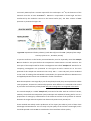
For instance, one of the most widely used types of semiconductor memory is flash memory
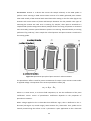
(EEPROM): data is retained for long period of time by transistors, which include the datasaving material under the gate (Figure 1). The operational principle is based on injection of
electrons by Tunneling mechanism into the floating gate [2]. Since electrical charge is retained
inside the gate, it switches the transistor into nonconductive state corresponding to the logical
0. When reverse Voltage is applied to the control electrode of such transistor, the electrons
are migrating back to the silicon and create the conductive channel corresponding to logical 1.
Figure 1. a. MOSFET and b. flash memory construction. c. Write operation: voltage applied to
the control gate causes a tunnel current to flow through the oxide layer, thereby injecting
electrons into the floating gate. d. Erase operation: voltage applied to the silicon substrate
releases the electrons accumulated at the floating gate [Image courtesy of TDK® Corp.].
Reducing the size of the elements, as another trend of high technology, leads to losses of
current through the thin gate dielectric layer. According to International Technology Roadmap
for Semiconductors reports and recent manufacturing technologies, the silicon dioxide is relic
since 2008, and enhancement of materials with larger value of relative permittivity is
mentioned as one of the way to overcome the size limits.
It is worth mentioning that even in transistors with another operating principles, e.g. NROM,
SHINOS and SONOS structures, electrons are stored in localized position, preserving a bit of
11
information [3]. These technologies are using mainly Si3N4 as a gate dielectric, however the
search for suitable materials still continues. The material should provide significant density of
charges per nano size local volume.
2.2. High-k dielectrics. Models of charge dissipation
Hafnium compounds are used for processors of 22 nm technology by Intel Corporation in 2013
[4]. Hafnium oxide (HfO2) satisfies the essential criterions for prominent high-k semiconductor
oxide, it is the most used and studied high-k. The requirements of a new oxide are [5]:
1) k value must be high enough to be used economically for a reasonable number of years.
2) The oxide is in very close contact with the Si channel, thus it must be thermodynamically
stable with Si.
3) The oxide must be kinetically stable, and able to be processed at 1000˚C at least for 5
seconds (in present process flows).
4) The oxide must act as an insulator, by having band offsets with Si of over 1 eV to minimize
carrier injection into its bands.
5) The oxide must form a good electrical interface with Si.
6) The oxide must have few bulk electrically active defects.
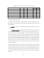
New candidate for gate oxide is required since 2009, despite the high k of Hf and HfO2:
Table 1. Comparison between semiconductors for probable replacing of SiO2 [5].
Besides the mentioned parameters, the locality of charge can be considered to be necessary
for storing the data in SONOS and NROM technologies. The locality can be measured by the
12
charge dissipation in the thin films by the measurements of surface potential. However,
precise device is required to track charge behavior: position, migration and dissipation.
Three main mechanisms are discussed to explain the charge dissipation [6, 7]:
1) Charge leakage into the conductive silicon wafer. This mechanism is driven by Tunneling
effect. The total injected charge Q is exponentially decreasing in time domain and observed by
decrease of local potential. Q is also called "integral charge" since it is calculated as the integral
of surface profile curve multiplied by surface area of the local charge.
2) Charge drift. It is described as the Coulomb repulsion of charges of same sign. This causes
lateral drift current 𝑗𝑑𝑟𝑖𝑓𝑡 = 𝜌 ∙ 𝜇 ∙ 𝐸. The total charge is not changing, but the same time local
potential is falling down concurrently with lateral widening of charged spot.
3) Diffusion mechanism. This mechanism of charge dissipation can be described as random
walk of charges via trapping centers. Total charge Q do not change, diffusion current is given
by formula 𝑗𝑑𝑖𝑓𝑓 = −𝐷 ∙ 𝛻𝜌, where D is diffusion coefficient and ρ is the density of charges.
Observed lateral widening for charged spot is proportional to t0.5.
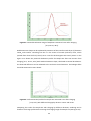
Results for ternary rare oxides (e.g. DyScO3 and GdScO3) have shown its promising conformity
for abovementioned six requirements with observed k ≈ 20 – 35. The studied Sc- based oxides
has shown even better values of k ≈ 28 – 33 with more appropriate morphology and energy
band structure [8 - 11]. Measurements of LaScO3 has shown its considerable locality in range
of hundred nm, though it is less than lateral size observed for SiO2 with embedded Si
nanocrystals (material SiO2 nc-Si), which was measured at best to be nearly 25 nm [11].
Figure 2. Experimental scheme of charge measurements by AFM. Injection, scanning [7].
13
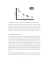
Further results for LaScO3 have shown the predominant mechanism of charge leakage, when
local charge observations were performed by Atomic Force Microscope. The scheme of
experiment is shown on Figure 2. A sharp tip of a Microscope is injecting charge by applying
bias voltage. Then AFM tip is scanning the surface to study the map of surface potential, thus
obtaining the values of potential decrease and lateral spreading with high accuracy.
It must be noted that tunneling was claimed as the main mechanism for LaScO3, however the
lateral widening was found. It was explained by diffusion inside the interface layer (IL). The
role of this oxide layer remains unclear. In literature was discussed one more La based oxide
LaLuO3 and it has shown even higher value of dielectric constant, k = 32. However
experimental data related to high-k applications is not available and its systematical study is
required according to authors of [8].
2.3. Properties and features of LaLuO3
LaLuO3 oxide thin films made of a stoichiometric ceramic target by Pulsed Laser Deposition
(PLD) has proven [8] its appropriate morphology of nearly 2 nm roughness (AFM),
stoichiometry by X-Ray reflectometry (XRR) La:Lu = 1:1.1 and dependence of dielectric
constant to the growth conditions [8, 11]. For instance the thermal method (PLD) has shown
higher results for k = 32 in nearly two times in comparison to the value for the film grown in
room temperature (k ≈ 17). Both internal photoemission (IPE) and photoconductivity (PC)
measurements have shown the value of energy barrier 5.3 eV. The Capacitance-Voltage (C-V)
measurements have shown low leakage current density, depending on the film thickness,
which resulted in calculating the Capacitance Equivalent Thickness (CET) giving the k = 32.
Further study of electrical properties of the LaLuO3 dielectric thin films was concluded as
significant.
14
3. Methodical Section
3.1. Scanning Probe Microscopy (SPM), fundamental and classification
Scanning probe Microscopy is the type of microscopy techniques, in which a physical probe is
scanning the sample’s surface. The start of this microscopy was established by foundation of
the Scanning Tunneling Microscope (STM) in 1981. In STM surface topography (map of the
heights with roughness) is measured by the tunneling current in vacuum between probe and
conductor [12]. Since many opportunities were presumed for technology of semiconducting
materials and insulators, structure of the microscope was developed to the construction with
small reflective cantilever plate, which reflected the laser light onto the photo detector.
Working principle became independent from conductivity, instead of it the Van der Waals
attractive-repulsive interaction revealed topography for solid materials and even liquids. This
construction, including the photo detector and cantilever is called Atomic Force Microscope
(AFM, 1986) [13]. Since these two devices provided significant enhancement in studying of
surface properties, their developers Binnig and Rohrer received Nobel Prize in 1986.
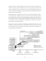
Figure 3. Types of Scanning Probe Microscopy. Family of KPM methods.
For the last three decades at least 30 other types of Scanning Probe devices have appeared.
They distinguish the information source: light radiation, noise, capacity etc. Each of them
permit measurement of specific forces (e.g. electrical forces, magnetic interaction). The basic
classification for SPM methods is given in Figure 3. It is impractical to discuss all the
possibilities of SPM, thereby this Thesis is oriented on special variety of techniques and modes,
i.e. AFM, KPFM and KPFGM (another name is KPFM Frequency Modulation).
15
3.2. Atomic Force Microscopy (AFM), main components and principle of operation
Atomic Force Microscopy (AFM) is an experimental method to study local properties of the
surface, based on Van der Waals interaction between a solid probe tip and the sample surface.
The first Atomic Force Microscope was invented in 1986 by G.Binnig, K.Quate and K.Gerber.
Due to nanometer sharpness of the tip probe, the AFM has nanometer and even subnanometer atomic resolution [13, 14]. Depending on the type of tip-sample interaction it
becomes possible to measure the local parameters of topography, surface potential,
mechanical properties (stiffness, adhesion, friction), magnetic properties etc.
Figure 4. Operational principle of AFM [Image courtesy of Connexions®, Rice University, USA].
The operational principle of the AFM is based on mechanical force between the probe and the
surface, and the measured system parameters are describing the relief (as opposed to the
STM, MSM and other techniques). A special detecting console is used to register roughness. It
is called “cantilever”, and include sharp tip at the end (Figure 4). Van der Waals interaction
defines the certain force acting the tip (corresponding to the SetPoint), however surface
roughness creates additional force, which results in bending of the cantilever. Then bending
angle is detected on the photo detector by shift of laser beam and recorded by system at each
point. Finally, tip’s trajectory profile is displayed as the scanned line.
Probe-surface interaction is described by attraction-repulsion model. When the tip is close to
the surface, then it is engaged in complex power interaction due to the elastic properties of
atomic shell [15]. It is possible to distinguish three areas of elastic impact, depending on value
of applied force as described in Figure 5.
16
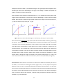
Figure 5. Lennard-Jones potential: equation and curve [15]. [Image courtesy of Soft Matter
Physics Division, University of Leipzig, Germany]
This Figure represents graph of the Lennard-Jones potential. In the left part of the curve can be
seen a sector of Contact Mode. The probe is in direct contact with the sample - it pushes the
surface. The strength of applied pressure is given by the system as the “SetPoint” parameter in
such way that tip do not create destructive impact to the material (it also depends on the
probe’s stiffness). Feedback system maintains the constant value of SetPoint < DFL ("Deflection
parameter" DFL corresponds to the measured force). Measurement results in the twodimensional map of measured surface “Parameter(x,y)”, e.g. if the parameter is height Z, then
image shows the Z(x,y), which is dimensional topography in every pixel of image (Figure 6).
Figure 6. Scheme of scanning process: red is straightway, blue is forward [16]. Data recording
is performed in straightway: j is number of pixel line, i is number of position; i, j = 256 – 1024.
Relief in AFM can be measured in two possible regimes: Constant force and Constant distance
(Figure 7), depending on number of included feedback loops. It should be noted, that the
Contact Mode is not applicable for soft and living objects due to the significant forces used.
Perhaps it is the basis for precise measurements of solid specimen in metrology.
In the middle of graph of Lennard-Jones Potential (Figures 5, 8 a) it is possible to mark the area
of Semicontact Mode measurements. In this mode the probe performs harmonic oscillations
and it "rattles" sample’s surface. The impact is less than in Contact mode.
17
Figure 7. AFM Constant Force (a) and Constant distance (c) modes with topography (b, d) [16].
Initially the probe is vibrating with cantilever's resonant frequency with distance almost 100
nm above the sample without touching it. When vibrating tip is getting closer to the surface,
repulsive force is growing and amplitude of oscillations is decreasing, thus feedback system is
regulating the specified “SetPoint” value. Feedback commands the scanner to shrink, thus
sample is again moving from the tip until amplitude becomes corresponding to SetPoint. One
should note that while in Contact mode SetPoint > DFL, in Semicontact mode SetPoint <
amplitude (MAG). In such way the middle line of the cantilever trajectory is kept constant, this
distance from surface dZ is used as relief. Ideally dZ must be equal to half of Amplitude of
oscillations. In this case probe bites the surface in its slowest position and impact is more
gentle, even applicable for living cells.
Figure 8. a. Distance in Semicontact mode [16]. b. Principles of three AFM modes [17].
Non contact mode (See Figure 8 b) corresponds to the case when the tip is oscillating with its
own resonant frequency f0, and it is not touching surface at all. The half-amplitude of
18
oscillations is less than distance between surface and cantilever's middle line ZLIFT (lift height),
i.e. 10 – 100 nm. Usually this mode is not applied at room temperature due to the weak
dependence of tip-sample interaction from the distance. However this mode is widely used as
a part of “two-pass” technique. In this regime of AFM operation, in first pass (first scanning of
the line) the Semicontact topography is measured, and then on the base of the topography the
tip goes above the same line with constant specified uplift height Zlift. It seems like the tip
returns back to the left side of the image line and tries to show zero topography. In second
pass the strong long-range forces can be measured, e.g. electrostatic force in KPFM. The
measurement in second pass is more sensitive due to the absence of Van der Waals forces,
and also it is more precise due to the z-vertical gradient of measured forces. That is because of
the simple assumption that only tip's apex is interacting with point on the surface but not the
whole tip cone and rather big cantilever plate. In second pass such forces can be negotiated
and force influencing the tip is connected only to the apex, which gives correction to the
position of cantilever, found from equation (kT is cantilever’s spring constant) [16]:
∆𝑧 =
𝑑𝐹
𝑑𝑘 𝑇
Simultaneously phase angle is shifted (Q is Quality factor, i.e. measure of energy losses):
∆𝜑 =
𝑄 𝑑𝐹
𝑘 𝑇 𝑑𝑧
The phase shift of the cantilever Δϕ is measured by the block unit (in accordance to shift in
resonant change of DFL) regarding the exciting electrical signal. Since Quality factor and
stiffness are known for cantilever, thereby measuring the phase shift it is possible to calculate
the derivative of the force influencing the tip. It is worth noting that the derivative shows
sharper change in the force parameters, it can be tracked more accurately, e.g. in Chapter 5
will be compared results for KPFM and KPFGM.
The constituent elements of the AFM
For further detailed discussion of AFM capabilities it is necessary to describe its basic
components. One can recall 4 main elements of AFM scheme [16]: 1) probe attached to a
flexible cantilever; 2) piezo-scanner used to move the sample relative to the tip; 3) optical
detection system (laser and photo detector), providing information of the bending angle of
cantilever; 4) feedback system. In addition, it is possible to name few separate additional
components: measurement electronic unit, personal computer, vacuum pump, vibration
isolation table etc.
19
The probe. Probe is the starting element of the AFM setup. It is usually a pointed pyramidal
needle with tip angle 10 – 20 degrees, fixed on a flexible cantilever unit (Figure 9). Most often
tips have slightly elongated shape, but it can be considered as a perfect cone for simplicity.
Probes are made of Polysilicon or Si3N4. Dopants cause undesirable increase of apex radius R.
Figure 9. Scheme of the cantilever with tip in forced movement [16].
Three main parameters characterize the tips: 1) tip's apex radius (usually called as tip radius R);
2) cantilever elastic coefficient kT, and 3) cantilever resonant frequency w.
Tip radius is critical factor for limiting the resolution of AFM scanning, e.g. for 10 nm radius the
lateral resolution of topography is limited to few nm. Usually tip radius have rather large value,
from R = 30 nm for Tungsten coated, to R = 20 nm for thin Platinum coated and R = 2 nm for Si
tips without additional coatings. Coatings increase R (Figure 10), but they provide special
features, e.g. ability to measure electrical or magnetic properties. A tip coating seems to be
fragile and limits the possible voltage range for electrical measurements by ~ 10 V. If the metal
layer will be broken it can cause convolution effects seen in the measured topography.
Figure 10. SEM image of NN-T190-HAR5 tips: radius = 50 nm, angle = 12°. [Image courtesy of KTek Nanotechnology, NT-MDT, Russia]
20
Elasticity coefficient of cantilever kT is in interval 0.001 N/m - 10 N/m [17]. kT is related to the
𝑑𝐹
magnitude of displacement of the tip height ΔZ and force F by equation 𝑑𝑘 𝑇 = 𝑑𝑍.
The smaller kT, the more suitable probe is for measuring delicate specimen such as living cells
(typically 0.01 – 0.03 N/m). Large k values are used in tapping mode, since magnitude of the
forces is less to increase the scanning speed. For the correct working conditions, AFM tips
should provide the resonant oscillation properties. The resonant frequencies of the cantilever
oscillation have bandwidth 10 – 1000 kHz, labeled by manufacturers. Bending frequency is
determined by the formula [16]:
𝑤=
λ
𝐸𝐽
�
𝑙2 𝜌𝑆
where l is the cantilever’s length, E is Young modulus, J is a cantilever’s moment of inertia, ρ is
material density, S is the cross surface area and λ is numerical coefficient for different
vibrational modes (Figure 11).
Figure 11. Major mechanical modes of tip's bending vibrations [16].
Quality factor Q is related with resonant frequency f0 and width "df" of Mag(f) resonance
curve. For vibrating cantilever Q is a measure of energy loss of oscillation, f0 ~ 300 kHz, Q in air
is nearly 100 [18, 19]
𝑓0
.
∆𝑓
𝑄=
In UHV conditions Q grows by factor of few hundred, nearly 500. In addition, Q can lead to the
explanation of the increasing resolution of gradient mode mentioned earlier. Considering time
scale of amplitude change in force mode [18], it is
𝜏~
2𝑄
.
𝑓0
However, in phase modulation gradient method
𝜏~
1
.
𝑓0
Thus time scale τ is nearly 500 times smaller for UHV, which is reason for rise in spatial
resolution [19].
21
The Scanner. Scanner is a device that moves the sample relatively to the AFM probe to
perform raster scanning in AFM. Piezo-scanner consists of a radially polarized piezo ceramic
tube made usually of PZT material with metal electrodes coating on the four sides (Figure 12)
Scanners with constructions of plates and bimorph elements are also possible. Two types of
mounting the scanner are used. First is scanning “by sample”, when piezo is attached to a
sample holder (used in NTegra Aura device). Sample surface is moving and pattern is measured
more accurately, because optical detection system is not moving. Second assembly is scanning
performed “by probe tip”, when sample has a fixed position and piezo-scanner is attached to
the moving probe.
Figure 12. Operational principle of piezo scanner’s tube movement.
The piezoelectric effect is used for precise movements of scanner. Piezo ceramic resizes under
an applied voltage. The equation of the inverse piezoelectric effect [16]
𝑢𝑖𝑗 = 𝑑𝑖𝑗𝑘 · 𝐸𝑘 ,
where uij is strain tensor, Ek is electric field component, dijk are the coefficients of the piezo
coefficient's tensor. Tensor of piezoelectric coefficients depends on the properties of
piezoelectric ceramics.
When voltage applied to the x-electrodes have different signs, tube is deflected in the xdirection (See Figure 12, central image), same situation for y-electrodes. Thus, probe can be
laterally moved along the surface in the x-y dimension. Upon application to the z-electrode
22
voltage with respect to both x, y-electrodes (See Figure 12, right image) either elongation Δz or
shortening of piezo occurs depending on the sign of the voltage. It enables to displace the
probe in z-direction normal to the surface.
Thus movement of the probe in three dimensions (x, y, z) is possible for scanning. Scan areas
range from few nanometers to several tens of microns depending on scanner and the voltage
applied. Piezo-scanner in AFM can move probe relative to the sample in all three directions x,
y, z and scan with accuracy nearly 10-12 m [20].
Figure 13. Piezo ceramic disadvantages: a. nonlinearity; b. creep; c. hysteresis [16].
Piezo ceramics have deficiencies [16] which should be considered when measuring and storing
the scanner. First of all, nonlinearity of piezoelectric ceramics exists (Figure 13 a). This reveals
in deviation from the linear dependence of the change in piezo length with high unit voltage
(over 100 V/mm). Second effect is creep (Figure 13 b), which is the delay in response to the
controlling field V. This is usually seen in the first scanning point as appearance of a white strip
in left side of the frame. That’s why first point is usually cropped by imaging software and not
visualized. Third, some inaccuracy always exists because of hysteresis properties of piezo
ceramic tube to change the length in direction of the electric field (Figure 13 c). This is the
reason why measurement is carried at one direction, which is mainly forward (see Figure 6).
Photo detector. Photo detector is the device to measure the deflection caused by the force in
the AFM tip in real-time of scanning the surface (Figure 14 a). For this purpose the optical
detection system is used. It is measuring the bends of cantilever and consists of: a) 1 mW laser
source, which is pointing the beam onto a cantilever and b) 4-sectional photodiode measuring
the intensity of laser light reflected from the cantilever to each of its four sections (See Figure
14 b). In order to improve the reflection, a special coating is applied on the back side of the
cantilever, e.g. a thin metal film.
23
Figure 14. Simplified scheme of the feedback working principle (a) and photo detector (b) [16].
Before measurements the system is adjusted in such a way that laser beam hit the cantilever
and fall into the exact center of 4-cell photo detector. The intensity of light falling on each
section should be the same. When additional force F (for example, caused by the interaction of
the tip with the surface topography) appears in scanning, this leads to a bending of the
cantilever. Cantilever bending causes changing in the angle of the reflected laser beam, thus
observed shift of the laser spot at the photo detector appears. The presence of four sections in
photodiode permits measuring these small shifts by the difference in photocurrent from
different sections. Measurement of the angle of the cantilever deflection (DFL) allows
measuring the tip-surface interaction force.
In Figure 14 it is also shown the feedback system (FB). FB performs a regulation function to
maintain a constant influence on the probe (in a constant force regime it is F). Minimum
resolution of forces in the AFM can be calculated by [19]
𝛿𝐹 =
2𝑘𝑘𝐵 𝑇𝐵
,
2
𝑤𝑄𝑧𝑂𝑆𝐶
where B is frequency bandwidth and Z2osc is mean square amplitude of the cantilever vibration.
More specifically, when contact of the probe with roughness causes the cantilever to bend, the
position of laser beam on the photo detector changes. Misbalance in the photocurrent ΔIZ is
measured as difference in height Z because DFL ~ IZ [16]
24
Δ𝐼𝑍 = (Δ𝐼1 + Δ𝐼2) − (Δ𝐼3 + Δ𝐼4) .
Shift in horizontal axis is measured as LF ~ IL
Δ𝐼𝐿 = (Δ𝐼1 + Δ𝐼4) − (Δ𝐼2 + Δ𝐼3) .
Measured difference DFL/LF is used by a computer system which responds by compensating
voltage to the scanner to minimize the DFL/LF variation. Here should be noted, that nominal
force does not matter, it is only important to support the permanent force values.
Accuracy of the scanner positioning is almost 10-12 m and laser causes small inaccuracy.
Therefore, main scan artifacts appear due to the feedback delay of the scanner. To eliminate
artifacts, it is necessary to reduce the speed of scanning. Nevertheless, system performs part
of the transformations of constant slope and offset curves. As a result, the measurement
appears as checking the value of the measured parameter at a given point (x,y) on the scanned
area Parameter(x,y), averaged over the value for surrounding 8 points (Figure 15).
Figure 15. Algorithm of processing the relative measurement by nearest 8 points [16].
a. Measured values; b. Distribution by values; c. Selection of appropriate value by exclusion.
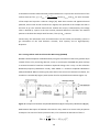
3.2.1. Electric Force Microscopy (EFM)
Electric Force Microscopy is a “two-pass” technique, which enables to obtain not only the
topography, but also the surface potential U, resulting in map U(x,y) [21]. Each line of the AFM
frame is scanned twice. Semicontact mode is called the "I pass" and it measures surface
topography. In the "II pass" non-contact AFM is performed, probe moves over the surface at a
distance of Zlift and repeats the trajectory measured in the "I pass". Additional voltage
25
𝑈 = 𝑈𝑑𝑐 + 𝑈𝑎𝑐 𝑆𝑖𝑛(𝜔𝑡)
is applied between the probe and the surface. Thereby, AFM-probe must be conductive, e.g. it
must be coated with a metal layer (usually Pt or Au). The electrostatic interaction energy of the
probe with the sample is
𝐶𝑈 2
𝐸=
,
2
where C is the capacitance between probe and surface. This capacity depends on the zdistance between the probe tip and the surface. Z-component of the electrostatic force acting
on the probe is
𝑑𝐸 𝑑𝐶 𝑈 2
𝐹𝑧 =
=
.
𝑑𝑧 𝑑𝑧 2
In this case, the derivative is negative for electrostatic attractive force. Since the applied
voltage is changing periodically, the interaction force between the probe and the surface will
also change periodically
𝐹(𝑧, 𝑡) =
1 𝑑𝐶
(𝑈 − 𝑈(𝑥, 𝑦) + 𝑈𝑎𝑐 sin(ωt))2 ,
2 𝑑𝑧 𝑑𝑐
where U(x,y) is the local value of surface potential at the certain position (x,y) below the AFM
probe. The equation for the force can be divided into three terms, distinguishing the part FDC
which is independent of frequency ω, from the first and second harmonics by ω [19]:
𝐹𝐷𝐶 =
𝐹𝜔 =
1 𝑑𝐶
2 𝑑𝑧
1
�(𝑈𝑑𝑐 − 𝑈(𝑥, 𝑦))2 + 𝑈𝑎𝑐 2�,
2
𝑑𝐶
(𝑈 − 𝑈(𝑥, 𝑦))𝑈𝑎𝑐 sin(𝜔𝑡) ,
𝑑𝑧 𝑑𝑐
𝐹2𝜔 = −
1 𝑑𝐶
𝑈𝑎𝑐 2 cos(2𝜔𝑡 ).
4 𝑑𝑧
It can be seen that the first harmonic of the electrostatic force Fω depends on the local value of
the potential U(x,y) for the AFM probe. Amplitude of the forced oscillation frequency
measured in "II pass" for the cantilever at ω is proportional to the magnitude of the first
harmonic of the electrostatic force Fω. Since the values of dC/dz, UDC and UAC are recorded in "II
pass", the resulting mapping of Fω(x,y) will contain information only about the distribution of
the surface potential U(x,y). Force accuracy in this method is piconewtons. It should be noted
26
that the measured difference ΔV includes not only the capacity value of the probe and the
sample, but also local potential value CPD [19]. This value characterizes the local properties of
the surface heterogeneity (influencing the magnitude of the electron work function), and the
embedded charge, which will be described for the case of KPFM.
3.2.2. Kelvin Probe Force Microscopy (KPFM)
KPFM is a “two-pass” microscopic study of surface potential [22, 23]. KPFM is similar to the
principle of EFM. Topography is measured in "I pass" Semicontact mode. After that, probe is
uplifted and in "II pass" the magnitude of electrostatic interaction of sample with an oscillating
probe is studied. Thus, topography roughness (Van der Waals interaction) is denied, while tip is
used as a reference electrode. KPFM differs from EFM because in "II pass" an additional
feedback loop to the voltage UDC is applied, so that Fω vanishes. It is achieved when voltage
applied to the probe UDC begins to change and adjusts to the feedback as long as Fω not equals
to zero at each scanned point Z(x,y). This occurs if 𝑈𝐷𝐶 = 𝑈 (𝑥, 𝑦), then values for certain
points is recorded by system as local value of U(x,y). Therefore map of the surface potential is
obtained. KPFM provides the highest lateral resolution of local potential measurements in
comparison to all other techniques: KP, PES, SEM (See Table 2). KPFM was first presented by
Nonenmacher in 1991 [24], and method is recommended as unique tool to characterize the
electric properties of semiconductor-metal surfaces and semiconductor devices at nanoscale.
a. b.
Figure 16. Demonstration of (a) AFM tip used for KPFM [25] and (b) Kelvin Probe [26].
27
It should be noted that measured local potential difference is equal to the work function of the
surface electrons 𝑈(𝑥, 𝑦) = 𝑉𝐶𝑃𝐷 =
𝜑𝑡𝑖𝑝 −𝜑𝑠𝑎𝑚𝑝𝑙𝑒
−𝑒
, where ϕsample and ϕtip are work fucntions
of the sample and tip and e is electron charge [19]. With direct contact and applied electrical
potential, Fermi levels of both materials are aligned, thus potential of the sample will shift to
the level of tip. The external electrical bias nullifies the current, simultaneously the voltage
value is defined by system as the local contact potential difference. Therefore this method
permits to calculate the sample work function, if the tip's ϕtip is known.
Concurrently, the information from second harmonic can be further processed by system to
get information of the local dielectric constant, local capacity and its high-frequency
dispersion.
3.2.3. Force gradient mode in Kelvin Probe Microscopy (KPFGM)
KPFGM is the development of KPFM mode by using the information of the force gradient dF/dz
instead of force F for processing data [19, 21-23]. In second pass of KPFGM the phase shift Δϕ
is measured instead of cantilever oscillation amplitude change. This is why it is also called the
KPFM-FM (Frequency Modulation mode), while KPFM is a common Amplitude Modulation
(AM) mode KPFM. When measuring the phase shift of the resonance cantilever oscillation, the
resolution is considerably higher (Table 3) than that for amplitude measurement (Figure 17).
Figure 17. Comparison between Amplitude Modulation (a) and Frequency Modulation (b) [19].
Mathematical description of KPFGM is discussed in many works as it seems to be perspective
technique. The essence of theory becomes clear, if we calculate the derivative of force F:
𝐹𝐷𝐶 =
1 𝑑𝐶
(𝑈𝑑𝑐 − 𝑈(𝑥, 𝑦))2 ,
2 𝑑𝑧
28
𝑑𝐹 1 𝑑 2 𝐶
=
(𝑈𝑑𝑐 − 𝑈(𝑥, 𝑦))2 ,
2
𝑑𝑧 2 𝑑𝑧
which corresponds to the phase shift
𝑄 1 𝑑 2𝐶
∆𝜑(𝑥, 𝑦) =
(𝑈𝑑𝑐 − 𝑈(𝑥, 𝑦))2 .
2
𝑘 2 𝑑𝑧
Thus, by measuring the phase angle dependence of U(x,y)2 and finding its minimum, it
becomes possible to define U(x,y) with significant accuracy [21, 27]. The accuracy is better
because dF/dz substantially decreases the electrostatic interaction of the sample with tip cone
and cantilever, which both seem to be considerable, but independent from z, i.e. dConst=0.
Table 2. Comparison of methods of measuring the surface potential [19].
Method Description
Energy Resolution
KPFM
Measuring local CPD of the sample surface
5-20 meV
KP
Measuring CPD of the whole sample surface
1 meV
PES
SEM
Measuring energy spectroscopy of the
whole sample surface
Spatial
resolution
Better than 10
nm
50 nm [26]
Better than
20 meV
100 nm
Measuring electron beam induced current
Not a quantitative
Better than 70
to map the surface potential
method
nm
When comparing -AM and -FM methods of KPFM one should mention that, regardless the
lateral resolution of the KPFM-FM is higher, data is usually recorded in degrees of phase shift.
This is because KPFGM mapping is based on distortion of the phase fluctuations. In order to
get values in mV, special conversion is required.
Table 3. Typical spatial and energy resolution of FM and AM mode KPFM [19].
KPFM
mode
FM
AM
Energy resolution
Spatial resolution
(meV)
Possibly sub-nanometer resolution depending on tip apex
Typically 25 nm (sub-nanometer resolution also possible
depending on sample)
29
10-20
5
3.3. Nanolithography of charge
Atomic Force Microscope is not only the instrument to study surface, but also a device
providing modification of the surface condition in nanometer scale. Firstly, the sharp probe tip
can be used in manipulating atoms [28], however for large solid samples it is possible to call
another valuable option of AFM - the lithography.
Programmably controlled tip movement can be combined in this technique with applying the
impact force, i.e. strong pressure or electrical voltage, to obtain the modified atomic state on
the surface during the tip's trajectory drawing. Since the "scanning" regime is operated in nondestructive impact, when system uses the mentioned SetPoint parameter to influence the
surface atoms only with elastic force, the "lithography" is different by the enlarged value of
“SetPoint” (for mechanical modifying). Second possibility occurs when the external voltage is
applied to the tip in accordance to the sample. With charge nanolithography it becomes
possible to inject the required amount of electrical charges into the sample (usually dielectric)
which could be used to deposit information in bits. Another option is oxidizing the small area
of semiconductors in transistor technology.
Two possible regimes of movement can be distinguished in nanolithography. They are
separated by the type of used sample image and tip movement consequence. The first
algorithm is called Vector lithography. It uses the specified commands of tip trajectories as
simple geometrical objects: squares, points, lines, circles etc. High operating speed is the main
advantage of Vector lithography. In our work the charging experiments were performed with
this type of Nanolithography by using points to inject the charges.
The second algorithm is called Raster lithography, because it uses the raster images to obtain
information of the required impact. The tip is moving by the whole image line by line as pixels
are measured to obtain value of color intensity. While AFM scanning measurements are
providing mapping by desired Parameter(x,y), in Raster lithography the system uses
information of every pixel to result its color intensity on the specimen. This type of lithography
was tested in our work (See Section 5.3) to obtain microscopic image of LUT logo.
30
3.4. State-of-the-art systems for SPM
The equipment for surface investigations has been developed, since it has shown prospects for
high technology applications. The first topografiner was invented in 1972, which gave the basis
for construction of STM [29]. A large variety of other Microscopes was launched by scientific
groups, however first prototypes are usually intended to be single-option devices [30].
Nowadays, multifunctional devices have appeared which provide opportunities for
comprehensive and precise investigations. Few prominent SPM platforms can be briefly
mentioned. Each of them offers appropriate features.
3.4.1. "NT-MDT NTegra AURA" device features
NTegra Aura device is the SPM for studies in the controlled conditions of low vacuum,
gases/liquids and external magnetic fields with more than 40 measuring modes included [31]:
STM, AFM (contact, semi-contact, non-contact), MFM, EFM, SCM, Kelvin Probe Microscopy,
Lithography etc. This allows investigating physical and chemical properties of the specimen
with accuracy almost 2 nm. The system permits high frequency regime of operation, which is
essential for vibrating oscillations in Semicontact mode. At the same time sensitivity of the
synchronous detector is up to 0.01 degree. Scanning system realizes the scanning by sample,
scanning by the probe and double scanning modes of operation. Maximal scanning field is
limited by 0.2 mm x 0.2 mm x 20 μm with scanning step nearly 0.001 nm. Device was used in
this work. Its main internal components are presented on Figure 18.
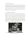
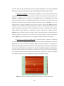
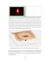
Figure 18. NTegra Aura device without vacuum hood [Image courtesy of PortalNano.ru,
Ministry of Education and Science of Russia].
31
3.4.2. "BRUKER Multimode 8" device features
Multimode 8 device provides opportunity to use a variety of SPM methods with highest
resolution and operational speed. It has optional modes to develop the system parameters
and possibilities. However, the most commonly used modes are included in basic construction:
AFM, STM, PhaseImaging, MFM, KPFM PeakForce, Torsional Resonance mode etc. [32]. This
device is operated with the ScanAssyst technology to simplify the operational algorithms for
researcher. Some of the modes are proprietary: ScanAssyst, PeakForce KPFM, PeakForce Tuna
mode etc. Device provides a larger variety of operating conditions and scanners from
400x400x400 nm to 125x125x5 μm and capable to investigate the mechanical properties of
fragile objects, polymers and living cells [33].
3.5. Advances in SPM equipment and techniques
In works [19, 21, 23, 28] are presented calculations of the advantages of the vacuum for AFM
scanning. It is explained in view of the increasing of Quality factor of the cantilever's
oscillation, because less amount of gas molecules are hitting the tip. Vibrations become easier
and their magnitude (MAG) increases. Thus it is possible to decrease the system multiplying
parameters which cause additional noise. At the same time, vacuum has a drying effect and
water layer covering the sample disappears. It can lead to better interpretation and accuracy
of the results, because water layer conceals the adhesion and accelerate the charge leakage.
Few research groups are still considering the properties of the liquid [34 - 36] in their works
and they describe the mechanics of the water layer-tip interaction as well as water-sample.
They are also studying the properties of ionic liquids [36] on the specimen and the affection of
viscous liquids to the results of scanning. These investigations seem necessary to be
implemented in living cells investigation due to the fragile structure of the cell membranes
(which are also covered by liquid layer). Progress in this study is expected in 2015 (Figure 19).
Distinguishing of the mechanical properties can result in the additional information about the
surface adhesion, stiffness and phase [32, 33]. The development of the mathematical basis of
such systems has already been used by Multimode 8 device PeakForce QNM mode.
The main claim of the research groups is that tip structure seems to be predominant factor in
scanning resolution. Some researchers adhere to the idea of sharp nanometer thin tips, even
consisting of one carbon nanotube. However in Binnig and Rohrer works in the 80s, authors
32
already stated as fact: though monatomic tips are necessary for STM, the shape of AFM tips
should be cone-like [37]. The fundamental work on the increasing of the resolution and
contrast in KPFM had resulted in the idea of not sharp, but blunt elongated tips [38]. Tips
should be accurately calibrated [39], and long durable probes providing high spatial resolution
for SPM is predicted until 2015 [40].
Remarkable attention in enhancement of AFM is put to the 2-pass technologies of AFM, or
even multitip platforms “Millipede” [40, 41]. This construction allows measuring the surface
with increased speed and can be used in Nanolithography for production of precise marks on
the coatings to save data. The multiprobe scanning probe microscope (SPM), in which several
tips or cantilevers are moved independently, is supposed to be a versatile tool for electrical
characterization at nanometer scales [28].
A big amount of works is discussing the developing of chemical bond study, due to the
opportunities to detect electrical forces at sub-nanometer range [40, 42]. Here can be noted
that some details of chemical interaction and chemical reactions can be studied using the
Scanning Probe Microscope platforms.
Figure 19. Roadmap of EFM family by 2006 [40].
33
According to [28] atomic manipulation will become a common procedure in nearest future.
The Scanning Probe Microscopy Roadmap 2006 also calls Nanolithography as one of the most
probably enhanced techniques in nearest decade [40].
Finally, it is worth saying that development of the data analysis could become as one of
probable advantages in SPM, for example in study of the KPFM-FM. Due to the improved
resolution of this method it can be used to obtain the map of electrical properties. However,
special treatment should be performed to obtain values of potential. Partly this problem had
been solved by AFM research group in Ioffe Institute.
3.6. Software for data and image processing
Software is used in Scanning Probe Microscopy at two stages: to process the data (feedback)
and to handle the scanned images. Since all algorithms of processing the data have the same
mathematical basis, though with details, certain image processing programs are strongly
valuable. Many purchasers of SPM platforms have their own appropriatory packages, e.g. in
this work is used NT-MDT “Nova Image Analysis”. “FemtoScan" can be supposed also as a
multifunctional instrument of analysis, while among the freeware programs can be mentioned
"Gwyddion" [43], which relies on processing the images for a variety of file formats (it is
working in shade tones). Here should be clarified that all images obtained in scanning are
made with imitational colors, since SPM is not an optical method [44]. All images in the Results
Chapter are presented in the red-black tones.
34
4. Experimental Part
In this Chapter the methodology of our study is presented with experimental sequence. One
can confidently suppose that the experiment is largely dependent on the available information
about the samples. Without denying the chemical law of definite proportions, method of
growing the sample (regime and conditions), with preliminary visual information about the
sample, roughness, reflection, contaminants and fractures, seems highly significant. Frequently
the required information is missing. When measurements are carried out for other
researchers, often happens that they do not provide important information about their
materials for the background. It is a difficult question for Scanning probe microscopy
specialists to examine the surfaces properly. If any artifacts, contaminants etc. are even
macroscopic (apparent to the naked eye) then results of the experiment can be distorted. This
is associated with high locality of SPM measurements (now as a drawback of SPM): if the
measurements are performed on the defect or contamination area, then will be monitored
exactly the properties of these imperfections (instead of the sample material properties).
When formulating a task, operator of SPM device should consider the existing information
about the sample and abilities of microscope, i.e. the Modes. The definite impact to the
sample gives reaction in real-time and examiner relies on personal experimental sense.
However, critical mistakes can be prevented by an approximate first probe experiment.
General basics presented below, including system parameters (MAG, DFL, amplification, lift
height dZ, Voltage etc.) and sequence of handling the images, can be assumed as universal for
future investigations.
4.1. LaLuO3 thin films
Two samples of high-k dielectric lanthanum lutetium oxide were objects of our investigation.
Samples were obtained from the Laboratory of Research Center Julich (Germany) and they
looked like dark squares nearly 1 cm2 each. The first sample (it is further called "Sample #6"
due to its catalogue name) consisted of Si wafer covered with 6 nm thick LaLuO3 coating made
by MBE technique in room temperature. Due to the observed features (defects) of its
morphology, little attention might be paid on the basics of this method.
Molecular beam epitaxy is a technology based on the evaporation of material to the crystal
substrate wafer, applied in extra high vacuum conditions. It can be used for growing the
heterostructures and thin films, however MBE is exigent and rather slow method with growth
35
rate nearly 1000 nm/hour. Vacuum required for this technique is 10-8 Pa, the cleanness of the
materials must be at least 99.999999 %. Material is evaporated in heated tigel and then
transferred by the molecular source to the heated wafer [45]. The basic scheme of MBE
operation is presented in Figure 20.
Figure 20. Experimental facility scheme (a) and device (b) used for MBE. [Adopted from Image
courtesy of Gusev A.I., Academic, Russia]
To prevent confusion in the further presented Results, must be separately noted that Sample
#6 was divided in two parts before the temperature measurements to avoid overheat. The
exact part of the sample used for further investigations was called "Sample 6.2". Results for its
comparing investigations are presented on the Figure 38 and in Section 5.2.4. The own
potential of this sample was measured to be nearly -0.8 V – -0.6 V and partly it was attributed
to the noise of working Thermal Module. Nevertheless, the potential difference between own
and applied potential values was considered in further calculations.
Note that Sample 6.2 was originally a part of Sample #6, thereby they were expected to exhibit
same properties, however the measured properties were different. It is assumed to be caused
by structural nonuniformity of Sample #6. Only two coatings were investigated in this work.
The second sample (it is called "Sample #7") consisted of Si wafer with 25 nm film of LaLuO3,
made by the Pulsed Laser Deposition (PLD) technique with additional heating 450˚C. PLD is a
preparation of coatings by condensation to the substrate surface of the products of reaction
between the target and with impulse laser beam with power nearly 108 W/cm2.
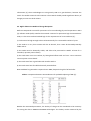
These methods are widely used in production of thin layers (See Table 4), each of them have
advantages and weaknesses. For our study only the quality of the surface is meaningful, and it
should be pointed out that MBE is considered to show excellent surface quality.
36
Table 4. Thin film deposition technique comparison chart [46].
ALD
CVD
Sputtering
PLD
MBE
Thickness uniformity
Good
Good
Good
Fair
Fair
Film epitaxy
Fair
Poor
Poor
Good
Good
Stoichometric uniformity
Good
Good
Fair
Good
Good
Number of materials
Fair
Fair
Good
Good
Fair
Low-temp deposition
Good
Poor
Good
Fair
Fair
Production yield
Good
Good
Fair
Fair
Poor
4.2. Sequence of the measurement
In this sequence is presented basic operational principles of Scanning Probe Microscope NTMDT NTegra Aura. The device allows measurement and operating of the data with Nova
software package.
Presetting. Preliminary, all the facilities should be turned ON and warm up for few
minutes.
1) The probe installation. Operating with the Scanning probe microscope is done not
only by the computer and SPM device, but also by the hands. Since probe installation is a
delicate procedure and it is performed manually, it is needed to follow the regular algorithm.
Firstly, the probe is taken from its box with adhesive coating on the bottom. It should be lifted
by the short side (probe is rectangular) with the help of tweezers. At this time, the small dots
on the long sides can be found by eyes though with difficulty. It is the cantilevers itself, with
length of nearly 150 μm and width 35 μm. Sizes can be noted descendingly: probe [5 mm] cantilever [35 μm] - tip [5 μm] - tip's apex [20 nm]. The cantilever is recognizable only with
optical microscope and tip’s apex is touching the surface, to observe its shape an electronic
microscope is needed.
The sample of investigation is placed on the polymer plate (made of policor protective
compound) and fixed. This plate is put on the scanner carefully, without applying too much
force on the fragile piezotube. Then the sample surface is electrically grounded to the Earth.
The measuring Head with probe holder should be placed above the sample in distance of 3
mm with the help of Head's screws. Otherwise tip can touch the sample and become rendered
unusable.
37
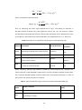
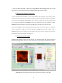
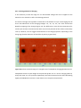
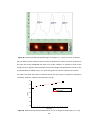
2) Setting the probe. Using the Nova software, in AIMING option the maximum value
for laser intensity on the photo detector should be obtained. Thus it is needed to turn the
screws of probe holder and the resulting red spot (cursor) should be situated nearly at the
center of AIMING window (See Figure 21: here DFL is below zero, LF is above zero). Close to
zero values for DFL and LF parameters would be desired. Changes of these parameters will be
used further by feedback system. After that, the laser spot should be placed right to the center
of screen by manually rotating the photo detector’s screws. Values of system intensity LASER
for platinum tips "fpN11Pt" and the Nova package are nearly 32 – 36.
Figure 21. Working window of the Nova program. Set regime is Semicontact; used option is
APPROACH; chosen parameter SetPoint is 10. Further mentioned options are seen at the left
up: DATA, AIMING, RESONANCE, APPROACH, SCAN, CURVES, LITHO. The system performs
measurements of MAG parameter. The AIMING window is seen at the right.
Finally, in the RESONANCE option it is required to find the resonant frequency for the
cantilever, which has the value of 100 – 200 kHz (indicated on the factory box). It depends on
the cantilever material stiffness, its length, temperature and individual features.
As it was told before, LASER parameter is the resulting value of light intensity for photo
detector. Due to the peculiarities of the reflection from the cantilever surface and the photo
detector’s positioning in space, the final setting of the probe must be conducted by the system
MAG parameter. For this purpose, in the APPROACH option with indicated DFL on the left, two
38
additional windows can be switched on to be indicated: 1) the AIMING spot and 2) a plot for
MAG in time domain (See Figure 21). With the help of photo detector’s screws, a maximum
value of MAG~15 is needed to be obtained.
3) Setting the scanner. At first, the electronic calibrations can be installed in the system
by pressing the “Settings” – “Load calibrations”. Except from this step, the scanner should be
mechanically calibrated. In Nova scheme active window the CLOSE LOOP, XY, NL buttons are
used for these purposes, followed by pressing the RUN button. On video screen or ocular of
the optical microscope there can be noticed movement of sample in respect to the cantilever
and its shadow. These calibrations are overwhelmingly important due to the nonlinear
mechanical properties of the piezo ceramic tube. The tube can stagnate with time and thus
creep effect will result in the image’s artifacts (see below). Finally, the buttons NL, XY, CLOSE
LOOP should be pressed again, in reversed order.
4) Creating the vacuum conditions. The safety hood should be put upside measuring
Head and sample. In NTegra Aura device, it is possible to protect the sample and measuring
system from acoustic noise and to obtain the depressurized atmosphere (this feature is
missing in BRUKER Multimode 8 basic configuration). In enhanced devices, the hood can
decrease the affect of electromagnetic noises and undesirable optical radiation. After the
pump is switched ON, the safety hood is plugged into the vacuum pipe.
Vacuum is used for many reasons, e.g. it creates the reproducible atmosphere, and it
minimizes the affection of dust particles (and gas molecules) to the cantilever and tip. This
increase the Quality factor Q. However, the most important effect of pumping is the drying
effect. The fact is that atmosphere air contains water molecules as moisture. Therefore, in
reality all the surfaces are covered by a water layer of few nanometers thickness. It can affect
the measuring regime of the AFM topography and also be the reason of charge dissipation. In
reduced atmosphere the surface tension of water is lowered down dramatically and thickness
of the aqueous water layer decreases. It is required to apply the additional heating up to 350˚C
to dry the surface completely, but it is apparent that sample and device are not suitable for
such heating. Residual water layer in our measurements is chemically adsorbed on the
dielectric surface and its thickness has a value of nearly 3 nm.
It must be noted that the resonant frequency parameter for cantilever f0 is changing in time
because of pumping. Frequency peak becomes narrow (Quality factor Q grows up) and shifts
to the left by few hundred Hertz. Simultaneously measured MAG parameter is growing up to
nearly 50 and it should be decreased by system amplification settings. Pumping lasts nearly
39
one hour until 10-5 bar and during this time it seems reasonable to set up the mentioned
parameters of scanner and probe and then check feedback for further measurements.
5) Setting the feedback. In the Semicontact Mode (it is used to protect surface from
scrapping for the first measurement, because it affects the surface less than Contact) the
SetPoint ≈ 0.6·MAG should be specified. In the APPROACH option, the LANDING button should
be pressed. By this action, the oscillating probe tip will come close to the surface and in few
seconds the defined system parameter MAG will become equal to SetPoint. This is the
demonstration of negative feedback, when system reaction is keeping the MAG parameter
constant in time. Thus the tip-surface influence is the same in all the measured areas of the
sample. Scanning in Semicontact mode is performed as the tip is oscillating with frequency
nearly 200 kHz, while cantilever is tracking the surface under the set distance (if lower
SetPoint, then the position under the sample is lower). One should keep in mind that distance
between cantilever and sample is not measured as numerical values, as well as the absolute
value of MAG is not necessary to know. It is enough that these parameters are constant.
6) Scanning in Semicontact Mode AFM. In the SCAN option “Frequency” parameter
should be set to 0.7 – 1 and chosen scan size to 10 micron, then press RUN button. It will take
approximately 5 min to finish one scanning image of that size. Further it is necessary to
process the topography results (See Section 5.1) and make decision about new scanning zone
in case of any found defects or asperities. One should remember that higher scanning rates,
varied by number of points and “Frequency” parameter, can lead to linear artifacts (See Figure
22, compare with results on Figure 28 b). At the same time, charges in our study are supposed
to be dynamic systems, thus it is needed to find optimum speed of scanning.
Figure 22. The raw image obtained for Surface Potential. It needs to be fitted.
40
7) Setting the Kelvin probe Mode. At first, the Kelvin probe Mode should be turned on
from Semicontact. Then operate the procedure of checking:
a. Open the “II pass” regime by the button of the same name.
b. Watch the MAG*SIN curve (this signal is proportional to electrostatic force Fw) on the
oscillograph in the right and turn off the feedback.
c. If MAG*SIN is on its maximum, then decrease the Lock-in Gain: then use “Amplitude” of
electrical stimulation nearly 0.2 – 0.5. By changing the phase of the generator, check that
MAG*SIN is crossing the horizontal axis, then set the phase for the maximum absolute value of
|MAG*SIN|. The sign of MAG*SIN should be taken such that if “Bias Voltage” is positive, then
MAG*SIN is decreasing. Concurrently it is required to monitor the noise level. Finally, check
that SetPoint=0; “FB Gain” is nearly 0.5 – 1.
d. Close the feedback loop, simultaneously check that MAG*SIN becomes zero.
e. Check the parameters of “II pass”, set SURFACE POTENTIAL to be measured.
8) Scanning in KPFM. a. Check that feedback is closed in “I pass”.
b. Measure the amplitude of oscillations in “I pass” to obtain the range for dZ.
c. Use the option CURVES and set the range to be 20 – 200 nm, then set the position of a
measured point by cursor and measure the amplitude (See Figure 26 in Results).
d. On the basis of this measurement set up the dZ parameter. If the amplitude of oscillation is
very small then leave it zero.
Figure 23. Image revealing artifacts caused by the excess value of lift height.
41
e. scan the surface by SCAN – RUN. For too high dZ the white damaged area will be seen
(Figure 23). It is required to decrease the dZ parameter due to these artifacts.
9) Charging & Lithography measurements.
In the LITHO option choose Mode “Vector” and Method “Bias Voltage”, then create the new
sample. It can be a point or a line. Then it is required to set the Voltage enough for lithography
on the basis of chargeability (See Chapters 5.2.1 and 5.2.4). After that, set the Contact mode
for scanning (remembering the SetPoint), unlock the feedback and set the “Feedback” to DFL.
SetPoint should be changed to be larger than DFL signal, and after that close the loop.
Finally, the charging is started by pressing the RUN button. To scan the result, it is needed to
set the Semicontact mode, set up the Feedback to MAG signal instead of DFL. Type in
SetPoint, which was used before in contact mode, then close the loop. Finally, the scanning is
operated by pressing the SCAN – RUN buttons.
10) Handle the obtained images.
Software Nova Image analysis can be used for this purpose (Figure 24). Second variant is
Gwyddion package. Nova seems to be more functional for appropriatory NT-MDT file formats.
Figure 24. The Nova Image Analysis main window, with settings on the right.
42
In the DATA option of Nova, press “Analysis” button on the right. Few operations as “Subtract
plane” are usually needed. To remove the feedback delay effects (artifacts), “Select Region”
option can be used: “Select region” – “Flatten correction 1D” – “Fit lines by area” – “Fit lines by
X” Exclude the area selected. To reduce the noise level, “Fourier Analysis” can be operated. In
the “FTT filtering” option it is needed to choose peaks except the central one.
As final result, the fitted and organized image is obtained. Therefore, it becomes possible to
measure potential, lateral size and other characteristics of the injected charge. Due to the
varying names of the settings and wide opportunities of the image processing software, they
seem to be out of range of this Master's Thesis.
Few artifacts can be named to be avoided in measurements. They appear due to:
1. Incorrect cantilever selection. For example, for living cells only those who have spring
constant 0.01 N/m should be selected. Some cantilevers have much larger stiffness, 5 – 10
N/m. By using such cantilevers to the soft objects, their surface would be destroyed in Contact
Mode. The information about softness is always mentioned by manufacturer.
2. Exceeded value of scan rate. When there is a small disturbance in the analyzed topography,
i.e. a hill, then tip position will be higher than the surface for some moment of time, however
cantilever is still moving. This can lead to the stretched lines after the roughness found in
Semicontact topography. At the same time tip is always returning to the start position on the
scan image (originally to the left side), thus the artifacts would be seen from the left side. The
light area on the Figure 23 does not mean that there is some object on the left of the image, it
is surely an artifact (Compare Figure 22 with the handled image on Figure 4b).
3. Incorrect lift height dZ. In KPFM when applying high values of dZ, drive amplitude would be
larger than possible for measurement of Surface potential. It is seen how tip slips upwards
from the sample because of the imperfections in the scanned surface (Figure 23).
The mentioned artifacts can be reduced by proper operation conditions. Thus the system
parameters, procedures and settings shown above seem to be valuable for practice. However,
some operations are called in different way in other systems and few items (calibration and
landing) can be done automatically in more advanced devices. Nonetheless, the experience
and skills are required for proper operation of the SPM. The results of measurements of
LaLuO3 presented below are obtained with the help of the methodology described above.
43
5. Results
5.1. Topography
The topography measurements demonstrated smooth surface (Figure 25) with 2 nm noise [8].
Figure 25. The 3D-recovery of surface topography for sample #6 with artifact on the right.
Few found artifacts did not affect the results of our experiments, at least for the future study
only the homogenously smooth surfaces were taken into account. To improve the resolution
of scans it was needed to find proper value of height, i.e. the Driving distance between the tip
and the sample in Semicontact mode, which was carried out by applying the proper "MAG"
system parameter nearly 2.0 – 3.0 [nA].
Figure 26. Mag(z) curve to define the Driving distance value in Semicontact Mode.
For correct measurements, the graph for Mag(z) (Figure 26) should be obtained straight
(irregularity due to the Young’s modulus is seen) and its slope multiplied by the "Mag" provide
nearly 80 nm amplitude for Semicontact.
44
5.2. Electrical charge behavior
Charging experiment includes two stages: 1) Charging of the point by Nanolithography
("LITHO" in Nova software) and 2) Measurement of the Surface Potential. As a result, the
topography scanning is operated in AFM Semicontact mode, the Surface Potential mapping is
made in second pass by KPFM. To check the ability of the samples for charging, the probe
measurement is needed. Thus, the probe potential +1 V (providing the potential difference of
nearly 1 Volt to the surface local potential) was applied for 10 seconds by the small sized tip’s
apex (approximately R = 20 nm for probes with Pt coating). To process the charge behavior
measurements it is necessary to define the real time on the scanned position (on the line of
the image). If the scan time length is 3 min 10 sec, but the desired spot is placed in the center
of the scan, then one can take the time for the charged point: 5 sec + 310/2 sec = 160 sec
(rather than zero or 310 sec). 5 seconds is the operational time for manual setting of the
“Surface Potential” mode from the “Nanolithography” (contact) mode used for charging. After
defining the existence of charged spot, +3 V 10 sec charging was used for control experiment
(See Figure 28b). The AFM results show clean smooth surface, while there is a charged spot on
KPFM. By automated measurement technique for the same position on the sample it is
possible to preliminary track the peak potential drop and evaluate lateral size and relaxation
time with non-destructive impact to a surface. To find the possible destructive potential
difference, the limiting potential experiment was arranged afterwards.
5.2.1. Electrical chargeability
The chargeability can be described as the value of surface response potential U in mV to the
voltage V applied to the tip, dU/dV.
250
Potential (mV)
200
150
100
50
0
0
1
2
3
4
5
6
7
8
Voltage (V)
Figure 27. Electrical chargeability of Samples #6 and #7. Note the green squares for positive
and blue squares for negative charging for Sample #6. Black curve is for their absolute values.
45
The chargeability of samples #6 and #7 (as linear slopes for red and black curves) differs nearly
in three times, which can be seen in the Figure 27. It is easier to inject the charge into the
Sample #6. Data is suggested to be given for same moment, however blue dots show slightly
lowered values due to the time difference. But the main reason for observed difference for
these charge injections will be discussed later. Here are given maximum values, obtained in
experiments with no loses occurring due to the surface defects or electrical system noises.
a. b.
Figure 28. KPFM results for Sample #6 after charging [+3 V, 10 sec]. a) AFM surface scan 10x10
μm2 is smooth; b) Surface Potential Mapping reveals charge in the center, FWHM = 365 nm.
Time for the observed drop potential is more than 1 h for Sample #6 and 0.3 h for Sample #7.
Peak is decreasing slightly and it has the bell shape, or so called "Gaussian" form (See Fig. 41).
sample 6 KPFM
sample 7 KPFGM
400
FWHM (nm)
300
200
100
0
0
1
2
3
4
5
6
7
Voltage (V)
Figure 29. FWHM vs. Voltage dependence for Sample #6 (KPFM) and Sample #7 (KPFGM).
Coordinate of expected intersection of the FWHM axis denotes operational limit for lateral size
in KPFM modes.
46
The full width at half maximum (FWHM) parameter is not changing in time in our experiment.
FWHM for Sample #6 is 365 nm [+3 V, 10 sec] (Figure 28b), while for Sample #7 it is estimated
as 360 nm. Thus the FWHM do not depend on the sample. Using the 20 nm thin Platinum tips
FWHM = 300 nm was achieved for Sample #7 (not presented here), however by using KPFGM
method lateral resolution is better than 100 nm in same conditions (Figure 29) [19, 27].
Though, the FWHM parameter strongly depends on the applied voltage. According to the
Figure 29, it is possible to track the linear approximation to the potential axis to find the value
for the maximum lateral resolution, about 250 nm for KPFM and 25 nm for KPFGM. Thus, the
KPFGM mode is preferable for the measurements because of better resolution, however it
cannot provide the numerical values of the Surface potential, because it is measured in
degrees of phase shift. That’s why for our further experiments KPFM mode was used, tracking
the values in mV (results for KPFGM see later).
One must admit that strange shape objects were found in the first measurements of Surface
Potential (See Figure 28b). The object can be described as ellipse with length nearly 2 μm,
highly negative core and positive cloud area shifted to the core (See Figure 30). The
concentration of these objects seemed to be nearly three on the 20 x 20 μm2 scan image. They
were preliminary distinguished as the surface defects, caused by mistakes in MBE method of
obtaining, thus the area with ellipses were not further examined.
a. b.
Figure 30. Surface Potential for ellipse shaped defects in Sample #6. a. Mapping; b. Profile.
47
a. b.
Figure 31. Surface Potential for defects after charging [+3 V, 10 sec]. a. Mapping; b. Profile.
Such artifacts should be distinguished in order to prevent affecting on the final measurements
of charge behavior. Although the ellipses have been perceived for the oddities, reaction to the
voltage applied was tested: it was found that average -28 mV core potential (Figure 30) is
increased up to the 140 mV (Figure 31), thus the potential difference is nearly 170 mV which is
in good agreement with the surface area without defects (compare with Figure 27). Still they
were not found in further KPFM scans and didn't affect the results.
Figure 32. 3D-reconstruction of the surface defect found in KPFM Surface Potential.
One can conclude that samples are uniformly smooth and chargeable: nearly 200 mV and 50
mV for samples #6 and #7 respectively in +3 V 10 sec regime. For more precise description of
charge behavior we conducted further research. The artifacts found in Sample #6 (See Figure
32) should be avoided.
48
5.2.2. Limiting potential of charging
It was necessary to find the range for non destructible voltage that can be applied to the
material in our research as well as the limiting potential.
The series of charges was injected to LaLuO3 film at the distance of 1 μm. The charging time of
10 sec was identical for all five charging voltages: -5V, -3V, -1V, +1V, +3V. Then we used the
KPFM for mapping of the charges (Figure 33). The difference in time of the measurement for
certain spot must be accounted at the same time as local potential of the surface itself (nearly
-0.02 V). However, one can suggest the difference in the charge properties, depending on the
charge sign (further discussion of the effect of polarity is given later).
Figure 33. Surface Potential image of a charged series for Sample #6, charging duration 10 sec.
Comparable results for peak height of the potential profile for +3 V 10 sec charging (180 mV,
nearly the same as in our previous experiment) was found. Potential curves were decreasing
slightly and FWHM was constant in time domain as in the previous experiment.
49
Figure 34. Surface Potential profile for the series of charges.
For sample #6 there are no observed limiting potential according to Figure 33 and potential
profiles shown in the Figure 34. The Sample #7 does not demonstrate the existence of critical
potential difference such as the Sample #6, at even wider range of -7 V – +7 V. We preferred to
use the +3 V 10 sec charging regime for ability to compare effects of temperature and time.
Critical Voltage for tips was nearly 10 V, thereby it was necessary not to go over this limit.
5.2.3. Induced charge relaxation time
Charge cannot be located within the dielectric layer for the unlimited period of time after
injection. This is observed when potential value U decreases. Relaxation time is the time
length, when the peak value of potential drops in e = 2.718 times. It is supposed to be one of
the main parameters of charge behavior, thus it is needed to define precisely the certain
potential values and real times of the measurements by algorithm described in Section 5.2.
The series of 3 points was injected in the Sample #6 to find the dependence of potential with
time Pot(t) for different charging duration: 1 sec, 10 sec, 30 sec (See Figure 35).
50
Figure 35. Surface Potential image of a charged series by duration. Charging voltage +3 V.
260
1 sec
10 sec
30 sec
240
220
Potential (mV)
200
180
160
140
120
100
80
60
40
0
500
1000
1500
2000
2500
3000
3500
Time (sec)
Figure 36. Potential height Pot(t) dependence for different charging duration for Sample #6.
The results for three charging times are shown in Figure 36. It is seen that charging time
reflects on the height of potential curve. Also it affects its shape, Gaussian becomes thicker.
FWHM and spot lateral size L become wider with increasing the duration of charging. The
relaxation time is more than one hour (not measured exactly in this experiment). It should be
mentioned here that after the experiments with charging on Sample #6, the measuring system
NTegra Aura was devacuumized. After 3 hours of reaction with ambient atmospheric air
(moisture and water film should be remembered), the charge spots were still visible (See
Figure 37). According to the potential height at start 198 mV, the result after 3 h was 58 mV,
i.e. fallen by 3.4 times, while FWHM increased only by nearly 30 nm.
51
Thus, Sample #6 shows high sustainability to the ambient conditions and remarkable
relaxation time of nearly 2 hours.
Figure 37. KPFM Surface Potential image of area after 3 hours on atmosphere (marked blue).
For the Sample #7 was carried out similar experiment with longer charging lengths: 10 sec, 30
sec, 90 sec. Relaxation time values were smaller, nearly 0.3 h. However, size of the spots was
nearly constant (FWHM ~ 360 nm) for all three injected charged spots and didn’t depend on
Potential (mV)
the charging length. Further investigation should be carried out on this issue.
sample 6
sample 7
sample 6.2
180
170
160
150
140
130
120
110
100
90
80
70
60
50
40
30
20
10
0
0
200
400
600
800
1000
1200
Time (sec)
Figure 38. Potential height Pot(t) dependence for Samples #6, #7 and 6.2 (cleavage).
52
Figure 38 shows comparison of the potential decreasing for different samples under similar
conditions: +3 V, 10 sec, room temperature. It is seen that both surfaces of #6 and #7 have
same Pot(t) ~ 1/t dependence. Results for “Sample 6.2” (See Experimental consequence in
Section 4.1) means the results of non-defect surface while the Thermal Module was turned
ON. Applied Voltage was even larger [+6 V, 10 sec], however, the measured potential for the
scanned area is 6 times smaller. One must note that such Module gave additional noise and
affected the resulting values. Still, the tendencies Pot(t) ~ 1/t are similar for all three presented
results. Second probability to describe the lowered values is by the impact of the defects on
Sample #6. Earlier it was considered to be negligible in our experiments, but defects could
partly result into positive outcome on charging. Still it can be justified to be only due the
Thermal module noise, however numerical values for charging, limiting potential and
relaxation time for Sample #6 presented here were justified to be correctly described.
It can be concluded that the amount of injected charge depends on the applied voltage, time
length of charging and the material properties. The relaxation time is 2 h for Sample #6 and
nearly 20 min for Sample #7, but it was not be precisely measured due to the low value of
Pot(t) for Sample #7 and high noise. After that it is possible to recall at least three other
factors, affecting the charges. It is needed to describe the tip form and height (not examined in
this work), temperature/pressure conditions, which also cause the additional layer of water
molecules [19] and the polarity of applied Potential difference.
5.2.4. Temperature dependence
The NTegra Aura Thermal Mode was applied to investigate the temperature dependence of
the charge behavior. It allows heating up to 150 °C in the vacuum conditions. The Sample #6
was prepared for the investigation (See Section 4.1). The average potential of the Sample 6.2
was -0.8 V, which must be taken into account while evaluate the time dependence below. The
charging regime [+6 V, 10 sec] was used for temperatures: 30°C, 50°C, 70°C, 90°C, 110°C.
Charging at 30°C is presented on Figure 39 a. Measured Pot(t) is smaller than expected.
It is seen in the Figure 40, that potential is decreasing slightly, as in the previous
measurements and showed Pot(t) ~ 1/t dependence. The expected decreasing with
temperature is connected to the rise in conductivity and mobility of charges within the
dielectric layer. However there is another conflicting effect that should be accounted. When
temperature is growing, the layer of the water molecules is getting thinner. The charge leakage
53
by this chemically adsorbed water film is terminated, thus potential should decrease more
slowly.
a. b.
Figure 39. KPFM Surface Potential image of Sample 6.2 after charging [+6 V, 10 sec, 30°C]:
a) t = 3 min, Pot = 31 mV; b) t = 17 min, Pot = 15 mV.
32
30
30 deg
50 deg
70 deg
90 deg
110 deg
28
Potential (mV)
26
24
22
20
18
16
14
12
10
0
200
400
600
800
1000
1200
1400
Time (sec)
Figure 40. Potential height Pot(t) dependence for different temperature conditions
for Sample 6.2 [+6 V, 10 sec].
In the case of the temperature measurements, one more probable effect was found in the
surface properties. One can see the complex structure of the potential profile for 30°C (the
first measurement) (See Figure 41, which is cross section of Figure 39 a). The potential curve
which had the bell shape earlier, here demonstrate the complex shape of two hills, which is
not concerned with curvature of the surface, it is the double Gaussian form. Such effect is in
accordance with the results for dielectric film with similar composition, LaScO3 [7, 10].
54
Figure 41. Potential distribution image of Sample 6.2 measured 2 min after charging
[+6 V, 10 sec, 30°C].
Double Gaussian shape can be explained by existence of the interface oxide layer (IL) between
LaLuO3 and Si-wafer. Tunneling into the IL is the reason of second (acclivous) curve, which
spreads faster than the first (narrow) curve. Time for this divergence was nearly 10 min. In the
Figure 41 is shown the potential distribution profile for Sample 6.2 after two minutes from
charging [+6 V, 10 sec, 30°C] with standard Gaussian shape, calculated as Normal distribution.
The observed difference can be admitted to the acclivous second Gaussian. This leakage effect
should be examined in more details.
Figure 42. Surface Potential profiles for Sample 6.2 measured 2 min after charging
[+6 V, 50°C] with different lithography duration: 10 sec and 30 sec.
Comparing the results for Sample 6.2 with charging by different durations, widening can be
found on the charge profile with increasing the charging length for Sample 6.2 (See Figure 42).
55
5.2.5. The effect of polarity of charge
While measuring the limiting potential for Sample #7, the difference in heights on the potential
profiles was observed (See Figure 43 a, c). The existing own average potential of Sample #7
was negligibly small about -0.02 V, thus it couldn't affect the results.
a. b.
c. d.
Figure 43. Surface Potential profile for a. Charges -7 V, +7 V; b. Charges +7 V, -7 V (reversed);
Surface Potential images of c. Charges -7 V, +7 V; d. Charges +7 V, -7 V (reversed).
It can be noted here that for Sample #6 such effect wasn't apparent (See Figure 33), because of
the experimental sequence: for the Sample #6 the mentioned series of charged points was
prepared for some operating time, assumed as: 10 seconds for charging of every next point
and additional 5 seconds for manual switching of modes. According to Figure 27 the
dependence of voltage is not absolutely straight: two points are higher (i.e. have larger slope)
than the others (See green line on Figure 27). These points are concerned with the positive +1
V and +3 V charging, while blue points are associated with negative voltages: -5 V, -3V, -1 V.
Thus, green and blue lines on Figure 27 for Sample #6 reveal dependence of polarity sign.
The polarity effect can be anticipated for both Samples #6 and #7. To prove the effect, we
interchanged the applied potential differences: from -7 and +7 to +7 and -7 to exclude the
factors of the measuring time (See Figure 43 b, d).
Still it was clearly seen that the positive peak is higher than the negative. The charging of the
material is easier with the positive applied voltage, than negative. It can be concerned with
difference in charge mobility, which should be further determined.
56
+7 V
-7 V
40
35
Potential (mV)
30
25
20
15
10
5
0
200
400
600
800
1000
1200
Time (sec)
Figure 44. Potential height Pot(t) dependence for different polarity signs for Sample #7.
The results for experiments with Sample #7 are presented in the Figure 44, which shows the
appropriate conformity of both measurements. Charging is easier in the case of positive
applied potential difference. The Nova software allows also calculating the total injected
charge (integral of the profile multiplied by the square surface is resulting in the volume of
potential), and it has shown 4 times more total value for the positive charging than negative.
5.2.6. Force gradient measurements
The Kelvin Probe Force Gradient Microscopy (KPFM gradient mode) was applied to define the
spot size with maximum lateral resolution. As it was told before, KPFGM provides measuring
the force gradient by phase angle shift in the degrees. According to our results, the maximum
resolution is on the range of 94 nm in experiments of charging the Sample #7 by +3 V 10 sec
regime (See Figure 29). A better locality was achieved both by KPFGM and by using thin 20 nm
Platinum tips. Resolution better than 250 nm was obtained by charging +7 V 10 sec for Sample
#7, which is thought to be nearly 570 nm for standard KPFM mode under the same mentioned
charging conditions. Thus it is possible to track the linear approximation for the red line on
Figure 29, which will give the result of nearly 25 nm for maximum lateral resolution for
KPFGM. This value is in agreement with the level of resolution of KPFGM discussed in literature
[27, 47].
The results for Sample #7 charging series of three points [+7 V, 10 sec] are presented on the
Figure 45, which was preliminary processed by uniform transformation in Nova image Analysis.
57
Figure 45. Potential profile and KPFGM image of charged [+7 V, 10 sec] series for Sample #7.
Still, the better lateral resolution doesn't allow to speculate the certain values for potential of
the spots and mainly KPFM-AM was used in our study. However it's possible to think of the
charge values in degrees and track down the Potential height time dependence similar to the
presented above for KPFM: Pot(t) ~ 1/t. Special programs for these transforms can be used.
The large noise level didn't allow to find the actual size of the spots L required for calculation
of mobility, diffusion coefficient and activation energy.
0,12
0,10
sample #6: Troom +3V 10 sec
0,08
L2(µm2)
Linear Fit of L2
0,06
0,04
0,02
0,00
0
500
1000
1500
2000
Time (sec)
2500
3000
3500
Figure 46. Experimentally obtained dependence of L2(t) of charge for Sample #6 [+3 V, 1 sec].
58
Nonetheless it is possible to evaluate the order of diffusion coefficient D from the Diffusion law
L2=D·t by considering L ≈ FWHM. Diffusion coefficient D is the slope of L2(t) seen in Figure 46. It
is measured to be nearly 8.5·10-10 cm2/sec. From the Einstein-Smoluchowski relation for
charges: D = μ·kB·T/q. Mobility μ can be estimated as 4·10-10 cm2/(V·sec). The values are in
accordance by order for similar semiconductor LaScO3 found in literature [7, 10]. Still it wasn’t
possible to precisely define the size of the charge spots for different temperature conditions
(in Section 5.2.4), which is necessary for defining the activation energy EA from the prescribed
Arrhenius law D = D0·exp(-EA/kBT).
5.3. Nanolithography observations
Considering the material’s property to store the injected charge for rather long period of time,
Nanolithography was tested on practical raster image. The raster sample - logo of the
Lappeenranta University of Technology, similar to the symbol “&” - was drawn in the 8 μm
variant on the surface of Sample #6 (See Figure 47). The applied Voltage range was -5 V to 0 V,
thus injected charge was negative to the background.
a.
b.
c.
Figure 47. Charge nanolithography in Sample #6. a. Starting raster sample image;
b. Image of the logo 2.5 x 2.5 μm2. Light area is 0 V, dark area is -5 V;
c. 3D-reconstruction image of the LUT logo.
The color gradation was not apparent for four supposed voltages. To obtain better resolution
and recognition, it was needed to consider the effect of polarity. While the positive charge is
injected easier than the negative, the positive potential difference should be associated with
the symbol, but not with the background. Thus, using the inversed (negative) lithography
sample and larger lateral scale the symbol become recognizable (See Figure 48).
59
a. b.
Figure 48. Charge nanolithography in Sample #6. a. Negative Sample;
b. Surface Potential image of the logo 8 x 8 μm2. Light area is 0 V, dark area is -5 V.
The charge was keeping its shape for a period of few minutes. It can be noted, that special
techniques of sample correction should be used in lithography of charge, as well as photomask
correction is performed in Photolithography.
Demonstration of lithography by charging the points in LaLuO3 thin films is a qualitative and
visible proof of the possibilities of NTegra Aura system, KPFM mode and the remarkable
properties of the investigated dielectric for Nanolithography.
60
Conclusions
1) AFM studies of surface topography indicated smooth and uniform surface of both 6 nm and
25 nm thick samples. The surface inhomogenities have range of 2 nm.
2) Structural artifacts were found in sample of thickness 6 nm (obtained by MBE technique) by
the Surface Potential studies in KPFM mode. The objects were up to 2 μm in diameter, had an
ellipse shape and consisted of negatively charged core with potential of -30 mV and positively
charged elongated cloud area with +140 mV. The background noise in KPFM was nearly 4 mV.
3) Samples of LaLuO3 are capable for the charge lithography, though their susceptibility to the
applied potential differs in more than three times. At room temperature and medium vacuum
conditions, value of the measured potential growth for +3 V was at level of 200 mV for 6 nm
thick film, while for 25 nm thick film the growth was nearly 50 mV. This can be corresponded
to the 4-fold distinction in sample width due to the formula 𝐸 ~ 𝑈/𝑑.
4) Lateral resolution for samples in KPFM with tungsten tips had range of 350 nm, the
application of thin platinum tips with radius of 20 nm increased resolution only up to 250 nm.
5) Lateral resolution of nearly 100 nm was achieved in KPFM gradient mode with thin platinum
tips, while maximum achievable resolution was estimated to be nearly 25 nm. Therefore,
KPFGM is more preferable for dimensional studies of area with injected charge.
6) Lateral size of the charged area was broadening with time as t0.5, i.e. in accordance with the
Diffusive model of charge spreading. In the first 10 min the injected charge is leaking from the
film to the substrate, which is revealed as decrease of the total charge Q and the existence of
double Gaussian shape on surface potential profile in first measurements, which is in
accordance to the data for the similar materials in literature. Tunneling into the interface layer
was established as the reason of partial decrease in total charge in LaLuO3 dielectric thin films.
7) Relaxation time for 6 nm thick sample is nearly 2 hours, while for the 25 nm sample it is
nearly 20 minutes. The potential level is decreasing proportionally to 1/t.
8) Charging time affects the size and the form of the surface profile. Increasing of the charging
duration lead to wider spot size, bigger value of potential and thicker Gaussian shape.
Temperature exposure decreases the potential which is caused by rise in mobility of charge
carriers. The influence of charging time and temperature effect can also be attributed to the
Tunneling of charge and Diffusive model of charge dissipation.
61
9) A polarity effect was found for LaLuO3, which is in contradiction with the literature data for
similar dielectric materials. It was determined that for LaLuO3 charge is more than in two times
easily injected by application of positive potential difference. This fact may be explained by
distinction in mobilities of charge carriers, but in any case the results for impact of polarity
should be further verified.
10) Influence of ambient pressure and moisture conditions was established. Depressed
atmosphere is causing the decrease of water layer thickness and contributes to the charge
retention and retardation of the potential decrease, which was demonstrated in the
temperature measurements for 6 nm thick sample.
11) At the same time LaLuO3 has shown high sustainability of injected charges in common
room conditions. It was demonstrated that after the device was devacuumized for 3 hours,
such room air and moisture exposure was followed by detection of charge still remaining in
the surface of dielectric layer for 6 nm sample.
12) Morphological difference between the two high-k coatings, obtained by MBE and PLD
techniques, was determined. 25 nm film made by PLD possesses better structural
characteristics of surface uniformity, which is compulsory for industrial applications.
Concurrently, the 6 nm sample obtained by MBE method had structural defects and the
increased capabilities for injection and reservation of charge for Nanolithography.
62
Summary
In this work LaLuO3 was investigated for the surface potential mapping by Kelvin probe
microscopy for the first time. Results for high resolution AFM measurements of surface
morphology are also demonstrated. For this purposes the methodology of Scanning Probe
Microscopy measurements was developed on practice. Measurements were conducted using
multifunctional NT-MDT NTegra Aura system, providing opportunity to study samples in
vacuum.
The main highlights of this work can be established:
1) By comparing the KPFM and enhanced KPFGM techniques, lateral resolution 300 nm and
100 nm respectively was obtained for LaLuO3 films.
2) The potential profile height is falling down proportionally to 1/t. Concurrently, the charged
spots were widening proportional to t0.5. The total charge Q is leaking into the interface layer
during first 10 min, after that Q do not change. At the same time with the complex shape of
potential profile the dominant mechanism of diffusion was established for charge dissipation.
3) The order for values of diffusion coefficient is 10-9 cm2/sec, the order for mobility is 10-10
cm2/(V·sec).
These values are significant for comprehensive studies and comparing of high-k dielectric
materials, they can be used to develop the technology of IC.
The establishing of the polarity effect should be emphasized. By applying the positive voltage
the total charge is nearly 4 times more stored and three times easily injected.
In this Master's Thesis the chargeability parameter was introduced for convenience, few
original pictures were created to demonstrate the occurring phenomena. For visibility issues,
the data was presented in graphs instead of numerical tables. The consequence of the study
was declared in advance and then followed. Thereby the general methodology integrated into
this study resulted in the conclusions of quantitative and qualitative criterions of future
prospects for LaLuO3 dielectric films. In purposes of methodical interest of this study, the
sequence of experiments was presented step by step, with system functions described and the
certain parametrical values for settings were given.
The definite numerical parameters can be further used for investigations of surface properties
and for verification of the results.
63
Few important weaknesses must be called for this research. Some shortcomings are associated
with the mentioned restrictions and could be evaded by inclusion of more functional
measuring systems. In particular, the numerical values for surface potential measurements
should be perceived with discretion, because the applied Thermal Module was causing high
level of interference noise. Mainly it was eliminated by using the Nova software for image
processing and the Fourier transforms. Presumably the noise was caused by grounding and
lowered the potential values. Nevertheless, the trend of potential drop is consistent with the
results of all the other experiments, thus it was justified to be correct.
The model describing charge behavior in view of Tunneling into the interface layer should be
overlooked with strong attention. In some models, the charge is leaking into the oxide layer
between semiconductor and silicon wafer, and only after that it is spreading by the diffusion
mechanism. Obtained results have shown constancy of spot size in time for some conditions.
The used tips did not allow the voltage more than 10 V. In future studies seems reasonable to
use blunt tips with lower resistivity for charge limit investigations.
The water layer affected the losses of total charge, because medium vacuum is not enough to
dry the surface properly. Inert gases atmosphere, high vacuum and heating (at least 350 deg)
are required to thoroughly dry the surface. This can be implemented in more enhanced
devices. However it was found that even medium vacuum conditions increase the Quality
factor of the probes for the experiment in more than 50 times.
In terms of the experiment, it would be worth to implement the line charging rather than point
charging, which is more relative to the actual industrial memory devices. Nevertheless, the
objective factors of measured potential decrease and charge spreading do not depend on such
form. Also the experiments aimed to determine the engineering parameter of capacitance
equivalent thickness (CET) associated with the relative value of dielectric constant supposed to
be carried out.
It is worth noting that at the time of using the device, few remarkable details were found on
practice, while attention to those is not clearly emphasized in the literature. For example, the
sample drift, caused by impact of the needle probe and thermal expansion had maxima as 5
micron per hour. Also noted: the existence of the wave front of charge divergence on the first
scans, non ordinary influence of structural defects on the properties of the sample, as well as
fragility and specific imperfections of the probe tips.
64
Finally, on the basis of the results along with review of literature related to the issue of Kelvin
probe microscopy, few possible ideas for further research can be named:
1) All the previously mentioned shortcomings should be eliminated. Especially errors in the
measurement of time.
2) Limitations of the measuring system can be overcome by using a more advanced device.
Thus ranges of exposure might be expanded: vacuum, heating/cooling, moisture content,
voltage etc. Also it can be possible to measure the mechanical characteristics, e.g. adhesion
and stiffness, which is possible in advanced systems.
3) Study the impact of the surface water layer and its properties, e.g. Newtonian properties,
also in case of ionic and viscous fluids. The forces occurring might be valuable in description of
SPM operation in different modes and Nanolithography of charge.
4) Study the impact of electromagnetic radiation on the LaLuO3 surface potential properties
and lithography, both in cases of dark/light conditions.
5) Using the developed methodology seems meaningful to study various classes of structures:
QDs, photovoltaics in light/dark, fiber materials, penometals, polymers, even biological
structures such as living cells.
6) To develop the computational methods of data analysis for different SPM modes and
conditions for more precise and automatic application. For example, to use different ranges of
tip-sample interaction force, which is still developed in devices nowadays.
7) Use more functional programs for image and data analysis and develop the processing
software to compare the materials suitable for high-k application.
The listed studies and development of experimental system may provide fundamental value
and can be used to improve the existing technologies.
65
References
[1] S.Sze, Physics of Semiconductor Devices (3rd Ed.), Wiley-Interscience, 2007.
[2] Dov Frohman-Bentchkowsky, Floating gate transistor and method for charging and
discharging same, Intel Corporation, Patent US3660819, 1972.
[3] Marvin H. White et al., Advancements in nanoelectronic SONOS nonvolatile semiconductor
memory (NVSM) devices and technology, International Journal of High Speed Electronics and
Systems 16 (2), 2006.
[4] S.Borkar, Design perspectives on 22 nm CMOS and beyond, Proc. 46th IEEE Design Autom.
Conf., pp. 93 - 94, 2009.
[5] J.Robertson, New High-K Materials for CMOS Applications, Comprehensive Semiconductor
Science and Technology, 2011.
[6] G.H.Buh et al., Real-time evolution of trapped charge in a SiO2 layer: An electrostatic force
microscopy study, Appl.Phys.Lett. 79 (2010), 1999.
[7] M.S.Dunaevskiy, P.A.Alekseev, P.Girard, E.Lahderanta, A.Lashkul, and A.N.Titkov, Kelvin
probe force microscopy of charge dissipation in nano thin dielectric layers, J. Appl. Phys. 110,
084304, 2011.
[8] J.M.J.Lopes et al., Amorphous lanthanum lutetium oxide thin films as an alternative high-k
gate dielectric, App. Phys. Lett. 89 222902, 2006.
[9] J.M.J.Lopes et al., La-based ternary rare-earth oxides as alternative high-k dielectrics,
Microelectronic Engineering 84, 2007.
[10] P.A.Aleksev et al., Locally injected charge behavior in nanothin films of LaScO3 high-k
dielectric on Silicon wafer, JTP Letters 39 (9), 2013.
[11] Y.Y.Gomeniuk et al., Electrical Properties of LaLuO3/Si(100) Structures Prepared by
Molecular Beam Deposition, ECS Transactions 33(3), 2010.
[12] G.Binnig, H.Rohrer, Scanning tunneling microscopy, Helv. Phys. Acta, vol. 55(6), 1982.
[13] G.Binnig, C.F.Quate, and C.Gerber, Atomic Force Microscopy, Phys. Rev. Lett. 56, 1986.
66
[14] Bharat Bhushan (Editor), Scanning Probe Microscopy in Nanoscience and Nanotechnology
(Vol. 2), NanoScience and Technology, Springer, 2010.
[15] Holger Schönherr and G. Julius Vancso, Atomic Force Microscopy in Practice, Scanning
Force Microscopy of Polymers, Springer Laboratory, 2010.
[16] V.Mironov, Fundamentals of Scanning Probe Microscopy, N.Novgorod, 2004 (in Russian).
[17] NanoWizard® Handbook, JPK Instruments (Version 1.3), p. 8, 2005.
[18] T.R.Albrecht et al., Frequency modulation detection using high‐Q cantilevers for enhanced
force microscope sensitivity, J. Appl. Phys. 69 (668), 1991.
19] W.Melitz, J.Shen, A.C.Kummel and S.Lee, Kelvin probe force microscopy and its application,
Surface Science Reports 66 (1), 2011.
[20] NT-MDT Ntegra Aura User Manual.
[21] M.S.Dunaevskiy, CSc Thesis: Atomic Force Microscopy of Si,Ge nanosmall insulas:
Methods of diagnostics and nanolithography of charge, S.-Pet., 2007, Ioffe PTI RAS (in Russian).
[22] S.Sadewasser, Th.Glatzel, Kelvin Probe Force Microscopy: Measuring and Compensating
Electrostatic Forces, Springer Series in Surface Sciences, volume 48, 2011.
[23] A.N.Titkov, P.Girard, Electrostatic Force and Force Gradient Microscopy: Principles, Points
of Interest and Application to Characterisation of Semiconductor Materials and Devices,
Applied Scanning Probe Methods II, NanoScience and Technology, 2006.
[24] M.Nonnenmacher, M.P.O'Boyle, and H.K.Wickramasinghe, Kelvin probe force microscopy,
Appl. Phys. Lett. 58 (25): 2921, 1991.
[25] NT-MDT Sover Next User's guide.
[26] Kelvin Probe information site, Accessed 17 May 2013,
http://www.kelvinprobe.info/introduction-surfaceanalysis.htm
[27] M.Dunaevskiy et al., Analysis of the lateral resolution of electrostatic force gradient
microscopy, J. Appl. Phys. 112 (064112), 2012.
[28] Franz J.Giessibl, Advances in atomic force microscopy, Review of Modern Physics 75, 2003.
67
[29] J. S. Villarrubia, The topografiner: An instrument for measuring surface microtopography,
in "A Century of Excellence in Standards", Measurements and Technology, NIST, 2001.
[30] Russell Young, John Ward, and Fredric Scire, The Topografiner: An Instrument for
Measuring Surface Microtopography, Rev. Sci. Instrum. 43 (999), 1972.
[31] NTegra Aura device Technical details from NT-MDT website, Accessed 20 May 2013,
http://www.ntmdt.com/device/aura-ii
[32] Bruker Multimode 8 technical details from BRUKER website, Accessed 23 May 2013,
http://bruker.com/products/surface-analysis/atomic-force-microscopy/multimode8/technical-details.html
[33] Barbara Foster, New Atomic Force Microscopy (AFM) Approaches Life Sciences Gently,
Qualitatively, and Correlatively, American Laboratory 24, 2012.
[34] T.Fukuma and S.P.Jarvis, Development of liquid-environment frequency modulation
atomic force microscope with low noise deflection sensor for cantilevers of various
dimensions, Rev. Sci. Instrum. 77, 043701, 2006.
[35] B.Reischl et al., Free Energy Approaches for Modeling Atomic Force Microscopy in Liquids,
J. Chem. Theory Comput. 9, 2013.
[36] Aleksander Labuda and Peter Grutter, Atomic Force Microscopy in Viscous Ionic Liquids,
Langmuir 28, 2012.
[37] G.Binnig, H.Rohrer, Nobel Lecture: Scanning tunneling microscopy-from birth to
adolescence, Rev. Mod. Phys. 59, 1987.
[38] H.O.Jacobs et al., Resolution and contrast in Kelvin probe force microscopy, J. Appl. Phys.
84 (1168), 1998.
[39] J.Hutter, J.Bechhoefer, Calibration of atomic-force microscope tips, Rev.Sci.Instr 64, 1993.
[40] Seizo Morita, Roadmap of Scanning Probe Microscopy, NanoScience & Technology, 2006.
[41] P.Vettiger et al., The “Millipede”-More than one thousand tips for future AFM data
storage, IBM J.Res.Develop. 44 (323), 2000.
[42] Leo Gross, Recent advances in submolecular resolution with scanning probe microscopy,
Nature chemistry 3, 2011.
68
[43] Gwyddion® software website, Accessed 17 May 2013, http://gwyddion.net/
[44] Yo.Shen et al., Simulating and interpreting Kelvin probe force microscopy images on
dielectrics with boundary integral equations, Rev. of Sci. Instrum. 79 023711, 2008.
[45] John R. Arthur, Molecular beam epitaxy, Surface Science Vol. 500, 2002.
[46] Joon Hyung Shim, Ph.D. Thesis "Nanoscale Thin Film Ceramic Fuel Cells", Stanford, 2009.
[47] M.S.Dunaevskiy et al., Nanolocal charge injection in thin SiO2 layers with an embedded ncSi by the AFM-tip, JTP Letters 33 (20), 2007 (in Russian).
69
Appendice I. List of Figures
Figure 1. MOSFET and flash memory constructions.
Figure 2. Experimental scheme of charge measurements by AFM.
Figure 3. Types of Scanning Probe Microscopy. Family of KPM methods.
Figure 4. Operational principle of AFM.
Figure 5. Lennard-Jones potential: equation and curve.
Figure 6. Scheme of scanning process in SPM.
Figure 7. AFM Constant force and Constant distance modes with topography.
Figure 8. Distance in Semicontact mode. Three principles of AFM modes.
Figure 9. Scheme of the cantilever with tip in forced movement.
Figure 10. SEM image of NN-T190-HAR5 tips: radius = 50 nm, angle = 12°.
Figure 11. Major mechanical modes of tip's bending vibrations.
Figure 12. Operational principle of piezo scanner’s tube movement.
Figure 13. Piezo ceramic disadvantages: a. nonlinearity; b. creep; c. hysteresis.
Figure 14. Simplified scheme of the feedback working principle and photo detector.
Figure 15. Algorithm of processing the relative measurement by closest 8 points.
Figure 16. Demonstration of AFM tip used for KPFM and Kelvin Probe.
Figure 17. Comparison between Amplitude Modulation and Frequency Modulation modes.
Figure 18. NTegra Aura device without the vacuum hood.
Figure 19. Roadmap of EFM family by 2006.
Figure 20. Experimental facility scheme and device used for MBE.
Figure 21. Working window of the Nova program.
Figure 22. The raw image obtained for Surface Potential.
Figure 23. Image revealing artifacts caused by the excess value of lift height.
Figure 24. The Nova Image Analysis main window.
Figure 25. The 3D-recovery of surface topography for sample #6 with artifact on the right.
Figure 26. Mag(z) curve to define the Driving distance value in Semicontact Mode.
Figure 27. Electrical chargeability of Samples #6 and #7.
Figure 28. KPFM results for Sample #6 after charging [+3 V, 10 sec].
Figure 29. FWHM vs. Voltage dependence for Sample #6 (KPFM) and Sample #7 (KPFGM).
Figure 30. Surface Potential for ellipse shaped defects in Sample #6. Mapping and Profile.
Figure 31. Surface Potential for defects after charging [+3V, 10 sec]. Mapping and Profile.
Figure 32. 3D-reconstruction of the surface defect found in KPFM Surface Potential.
Figure 33. Surface Potential image of a charged series for Sample #6, charging duration 10 sec.
Figure 34. Surface Potential profile for the series of charges.
Figure 35. Surface Potential image of a charged series by duration. Charging voltage +3V.
Figure 36. Potential height Pot(t) dependence for different charging duration for Sample #6.
Figure 37. KPFM Surface Potential image of area after 3 hours on atmosphere (Sample #6).
Figure 38. Potential height Pot(t) dependence for Samples #6, #7 and 6.2 (cleavage).
Figure 39. KPFM Surface Potential image of Sample 6.2 after charging [+6 V, 10 sec, 30°C].
Figure 40. Potential height Pot(t) dependence with temperature for Sample 6.2 [+6 V, 10 sec].
Figure 41. Potential distribution image of Sample 6.2, 2 min after charging [+6 V, 10 sec, 30°C].
Figure 42. Surface Potential profiles for Sample 6.2, 2 min after charging [+6V, 50°C] 10, 30 sec.
Figure 43. Surface Potential profiles and images for charges [-7 V, +7 V] and reversed position.
Figure 44. Potential height Pot(t) dependence for different polarity signs for Sample #7.
Figure 45. Potential profile and KPFGM image of charged [+7 V, 10 sec] series for Sample #7.
Figure 46. Experimentally obtained dependence of L2(t) of charge for Sample #6 [+3 V, 1 sec].
Figure 47. Charge nanolithography in Sample #6: raster sample, litho image, 3D-reconstruction.
Figure 48. Charge nanolithography in Sample #6. Negative sample and Surface Potential image.
Appendice II. History of
SPM
Appendice II (continued). Future technologies
(taken from [40] S.Morita - Roadmap for Scanning Probe Microscopy 2006)