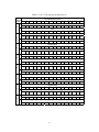
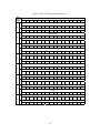
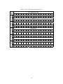
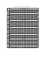
1
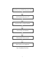
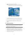
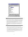
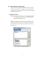
PCI-1780
8-ch Counter/Timer Card
User Manual
Copyright
The documentation and the software included with this product are
copyrighted 2002 by Advantech Co., Ltd. All rights are reserved.
Advantech Co., Ltd. reserves the right to make improvements in the
products described in this manual at any time without notice. No part of this
manual may be reproduced, copied, translated or transmitted in any form or
by any means without the prior written permission of Advantech Co., Ltd.
Information provided in this manual is intended to be accurate and reliable.
However, Advantech Co., Ltd. assumes no responsibility for its use, nor for
any infringements of the rights of third parties, which may result from its
use.
Acknowledgments
PC-LabCard is a trademark of Advantech Co., Ltd. IBM and PC are
trademarks of International Business Machines Corporation. MS-DOS,
Windows, Microsoft Visual C++ and Visual BASIC are trademarks of
Microsoft Corporation. Intel and Pentium are trademarks of Intel
Corporation. Delphi and C++ Builder are trademarks of Inprise
Corporation.
CE notification
The PCI-1780, developed by ADVANTECH CO., LTD., has passed the CE
test for environmental specifications when shielded cables are used for
external wiring. We recommend the use of shielded cables. This kind of
cable is available from Advantech. Please contact your local supplier for
ordering information.
On-line Technical Support
For technical support and service, please visit our support website at:
http://www.advantech.com/support
Note:
✎ Concerning environmental protection, to reduce the paper used for the
user’s manual. Starting the page of Appendix C, please use the PDF file
on the CD-ROM or download form support on www.advantech.com.
Part No. 2003178010
Printed in Taiwan
i
2nd Edition
May 2005
ii
Contents
1. INTRODUCTION.................................................................................................................. 1
1.1
FEATURES ....................................................................................................................... 1
1.2 APPLICATIONS ................................................................................................................. 3
1.3 INSTALLATION GUIDE ...................................................................................................... 3
1.4
SOFTWARE OVERVIEW..................................................................................................... 5
1.5 DEVICE DRIVERS PROGRAMMING ROADMAP .................................................................. 6
1.6 ACCESSORIES .................................................................................................................. 8
2. INSTALLATION.................................................................................................................... 9
2.1 UNPACKING ..................................................................................................................... 9
2.2 DRIVER INSTALLATION .................................................................................................. 11
2.3 HARDWARE INSTALLATION ............................................................................................ 12
2.4 DEVICE SETUP & CONFIGURATION................................................................................ 15
3. SIGNAL CONNECTIONS.................................................................................................. 19
3.1 OVERVIEW .................................................................................................................... 19
3.2
SWITCH AND JUMPER SETTINGS .................................................................................... 19
3.3
SIGNAL CONNECTIONS .................................................................................................. 21
APPENDIX A. SPECIFICATIONS........................................................................................ 25
APPENDIX B. BLOCK DIAGRAM ...................................................................................... 27
APPENDIX C. REGISTER STRUCTURE AND FORMAT ............................................... 29
C.1 OVERVIEW .................................................................................................................... 29
C.2 I/O PORT ADDRESS MAP .............................................................................................. 29
C.3
COUNTER 0/1/2/3/4/5/6/7 MODE — BASE+00/08/10/18/20/28/30/38H ...................... 36
C.4
COUNTER 0/1/2/3/4/5/6/7 LOAD — BASE+02/0A/12/1A/22/2A/32/3AH ................... 39
C.5
COUNTER 0/1/2/3/4/5/6/7 HOLD — BASE+04/0C/14/1C/24/2C/34/3CH .................... 40
C.6
COUNTER 0/1/2/3/4/5/6/7 COMMAND — BASE+06/0E/16/1E/26/2E/36/3EH ............. 41
C.7
COMMAND ENABLE — BASE+40H ............................................................................. 42
C.8 INTERRUPT CONTROL — BASE+42H........................................................................... 43
C.9 INTERRUPT STATUS — BASE+42H .............................................................................. 43
iii
C.10
CLEAR INTERRUPT — BASE+44H ............................................................................. 44
C.11 DIGITAL OUTPUT — BASE+48H................................................................................ 44
C.12 DIGITAL INPUT — BASE+48H................................................................................... 44
C.13
BOARD ID — BASE+4EH ......................................................................................... 45
C.14
FOUT 0/1/2/3/4/5/6/7 CONTROL — BASE + 50~5FH ............................................... 46
APPENDIX D. WAVEFORM OF EACH MODE ................................................................. 49
D.1
MODE A WAVEFORM .................................................................................................... 51
D.2
MODE B WAVEFORM ..................................................................................................... 52
D.3
MODE C WAVEFORM ..................................................................................................... 53
D.4
MODE D WAVEFORM .................................................................................................... 54
D.5
MODE E WAVEFORM ..................................................................................................... 55
D.6
MODE F WAVEFORM ..................................................................................................... 56
D.7
MODE G WAVEFORM .................................................................................................... 57
D.8
MODE H WAVEFORM .................................................................................................... 58
D.9
MODE I WAVEFORM ...................................................................................................... 59
D.10 MODE J WAVEFORM .................................................................................................... 60
D.11
MODE K WAVEFORM ................................................................................................... 61
D.12 MODE L WAVEFORM ................................................................................................... 62
D.13 MODE O WAVEFORM .................................................................................................. 63
D.14 MODE R WAVEFORM ................................................................................................... 64
D.15 MODE U WAVEFORM .................................................................................................. 65
D.16 MODE X WAVEFORM ................................................................................................... 66
iv
1. Introduction
Thank you for buying the Advantech PCI-1780. The PCI-1780 is a
general purpose multiple channel counter/timer card for the PCI bus. It
targets the AM9513 to implement the counter/timer function by CPLD.
It provides eight 16-bit counter channels and 8 digital outputs and 8
digital inputs. The powerful Advantech-designed counter functions
fulfill your industrial or laboratory application needs.
The following sections of this chapter will provide further information
about features of the multifunction cards, a Quick Start for installation,
together with some brief information on software and accessories for the
PCI-1780 card.
1.1
Features
❏ 8 independent 16-bit counters
❏ 8 programmable clock source
❏ 8 digital TTL outputs and 8 digital TTL inputs
❏ Up to 20 MHz input frequency
❏ Multiple counter clock source selectable
❏ Counter output programmable
❏ Counter gate function
❏ Flexible interrupt source select
❏ Board ID
The Advantech PCI-1780 offers the following main features:
Flexible Counter Modes
The PCI-1780 features up to 12 programmable counter modes, to
provides one shot output, PWM output, periodic interrupt output,
time-delay output, and to measurement the frequency and the pulse
width. The PCI-1780 is an ideal solution for variant counter/timer
applications.
1
Special Shielded Cable for Noise Reduction
The PCL-10168 shielded cable is specially designed for the PCI-1780
for reducing noise. Its wires are all twisted pairs, with input signals and
output signals separately shielded, providing minimal cross talk between
signals and offering the best protection against EMI/EMC problems.
Counter mode table:
(N: No gate control, L: Level gate control, E: Edge gate control)
Counter Mode
Special Gate (CM6)
Reload Source (CM5)
Repetition (CM4)
Gate Control (CM15~CM12)
A
0
0
0
N
B
0
0
0
L
C
0
0
0
E
Count to TC once, then disarm
Count to TC twice, then disarm
Count to TC repeatedly without disarming
Gate input dose not gate counter input
Count only during active gate level
Start count on active gate edge and stop count on next TC
Start count on active gate edge and stop count on second TC
Start count on active gate edge and stop count on inactive gate edge
Reload counter from Load Register on TC
Reload counter on each TC, alternating reload source between Load
and Hold Registers
✓
✓
✓
✓
D
0
0
1
N
E
0
0
1
L
F
0
0
1
E
✓
✓
✓
✓
✓
G
0
1
0
N
H
0
1
0
L
I
0
1
0
E
✓
✓
✓
✓
✓
✓
J
0
1
1
N
K
0
1
1
L
L
0
1
1
E
✓
✓
✓
✓
✓
✓
✓
✓
✓
✓
✓
Counter Mode
Special Gate (CM6)
Reload Source (CM5)
Repetition (CM4)
Gate Control (CM15~CM12)
M
1
0
0
N
N
1
0
0
L
O
1
0
0
E
Count to TC once, then disarm
Count to TC twice, then disarm
Count to TC repeatedly without disarming
Gate input dose not gate counter input
Count only during active gate level
Start count on active gate edge and stop count on next TC
Start count on active gate edge and stop count on second TC
Start count on active gate edge and stop count on inactive gate edge
Reload counter from Load Register on TC
Reload counter on each TC, alternating reload source between Load
and Hold Registers
✓
✓
✓
✓
✓
✓
✓
P
1
0
1
N
Q
1
0
1
L
R
1
0
1
E
✓
✓
✓
✓
✓
✓
✓
✓
✓
✓
✓
S
1
1
0
N
T
1
1
0
L
U
1
1
0
E
V W X
1 1 1
1 1 1
1 1 1
N L E
✓
✓
✓
✓
✓
✓
✓
✓
✓
✓
✓
✓
✓
✓
✓
✓
✓
✓
✓
✓
✓
✓
✓
✓
✓
Note: Counter modes M, N, P, Q, S, T, V, W are identical to A, B, D, E, G, H, J, K.
Note:
✎ For detailed specifications of the PCI-1780, please refer to Appendix A,
Specifications.
2
✓
✓
✓
✓
✓
✓
✓
1.2
Applications
❏ Event counting
❏ One shot output
❏ Programmable frequency output
❏ Frequency measurement
❏ Pulse width measurement
❏ PWM output
❏ Periodic interrupt generation
❏ Time-delay generation
1.3
Installation Guide
Before you install your PCI-1780 card, please make sure you have the
following necessary components:
❏ PCI-1780 DA&C card
❏ PCI-1780 User’s Manual
❏ Driver software
Advantech DLL drivers
(included in the companion CD-ROM)
❏ Wiring cable
PCL-10168 (option)
ADAM-3968 (option)
Personal computer or workstation with a
PCI-bus slot (running Windows 2000/95/98/
NT/ME/XP)
❏ Wiring board
❏ Computer
Some other optional components are also available for enhanced
operation:
❏ Application software
ActiveDAQ, GeniDAQ or other third-party
software packages
After you get the necessary components and maybe some of the
accessories for enhanced operation of your Multifunction card, you can
then begin the Installation procedures. Figure 1-1 on the next page
provides a concise flow chart to give users a broad picture of the
software and hardware installation procedures:
3
Install Driver from CD-ROM, then power-off PC
Install Hardware and power-on PC
Use driver utility to configure hardware
Use test utility to test hardware
Read examples & driver manual
Start to write your own application
Fig. 1-1 Installation Flow Chart
4
1.4
Software Overview
Advantech offers a rich set of DLL drivers, third-party driver support
and application software to help fully utilize the functions of your
PCI-1780 card:
Device Drivers (on the companion CD-ROM)
❏ LabVIEW driver*
❏ Advantech ActiveDAQ
❏ Advantech GeniDAQ
❏
Programming choices for DA&C cards: You may use Advantech
application software such as Advantech Device Drivers. On the other
hand, advanced users can use another option for register-level
programming, although it is not recommended due to its laborious and
time-consuming nature.
Device Drivers
The Advantech Device Drivers software is included on the companion
CD-ROM at no extra charge. It also comes with all Advantech DA&C
cards. Advantech’s device drivers feature a complete I/O function
library to help boost your application performance. The Advantech
Device Drivers for Windows 2000/95/98/ ME/NT/XP works
seamlessly with development tools such as Visual C++, Visual Basic,
Inprise C++ Builder and Inprise Delphi.
Register-level Programming
Register-level programming is reserved for experienced programmers
who find it necessary to write code directly at the level of device
registers. Since register-level programming requires much effort and
time, we recommend that you use the Advantech Device Drivers
instead. However, if register-level programming is necessary, you
should refer to the relevant information in Appendix C, Register
Structure and Format, or to the example codes included on the
companion CD-ROM.
5
1.5
Device Drivers Programming Roadmap
This section will provide you a roadmap to demonstrate how to build
an application from scratch using Advantech Device Drivers with your
favorite development tools such as Visual C++, Visual Basic, Delphi
and C++ Builder. The step-by-step instructions on how to build your
own applications using each development tool will be given in the
Device Drivers Manual. Moreover, a rich set of example source code is
also given for your reference.
Programming Tools
Programmers can develop application programs with their favorite
development tools:
❏ Visual C++
❏ Visual Basic
❏ Delphi
❏ C++ Builder
For instructions on how to begin programming works in each
development tool, Advantech offers a Tutorial Chapter in the Device
Drivers Manual for your reference. Please refer to the corresponding
sections in this chapter of the Device Drivers Manual to begin your
programming efforts. You can also look at the example source code
provided for each programming tool, since they can get you very well
oriented.
The Device Drivers Manual can be found on the companion CD-ROM.
Or if you have already installed the Device Drivers on your system,
The Device Drivers Manual can be readily accessed through the Start
button:
Start/Programs/Advantech Driver V2.0a/Device Driver Manual
The example source codes could be found under the corresponding
installation folder such as the default installation path:
\Program Files\Advantech\ADSAPI\Examples
6
For information about using other function groups or other
development tools, please refer to the Creating Windows 95/NT/2000
Application with Device Drivers chapter and the Function Overview
chapter on the Device Drivers Manual.
Programming with Device Drivers Function Library
Advantech Device Drivers offers a rich function library to be utilized
in various application programs. This function library consists of
numerous APIs that support many development tools, such as Visual
C++, Visual Basic, Delphi and C++ Builder.
According to their specific functions or services, those APIs can be
categorized into several function groups:
❏ Digital Input/Output Function Group
❏ Counter Function Group
❏ Port Function Group (direct I/O)
❏ Event Function Group
For the usage and parameters of each function, please refer to the
Function Overview chapter in the Device Drivers Manual.
Troubleshooting Device Drivers Error
Driver functions will return a status code when they are called to
perform a certain task for the application. When a function returns a
code that is not zero, it means the function has failed to perform its
designated function. To troubleshoot the Device Drivers error, you can
pass the error code to DRV_GetErrorMessage function to return the
error message. Or you can refer to the Device Drivers Error Codes
Appendix in the Device Drivers Manual for a detailed listing of the
Error Code, Error ID and the Error Message.
7
1.6
Accessories
Advantech offers a complete set of accessory products to support the
PCI-1780 card. These accessories include:
Wiring Cable
❏ PCL-10168
The PCL-10168 shielded cable is specially designed
for PCI-1780 cards to provide high resistance to noise.
To achieve better signal quality, the signal wires are
twisted in such a way as to form a “twisted-pair
cable,” reducing cross-talk and noise from other signal
sources. Furthermore, its analog and digital lines are
separately sheathed and shielded to neutralize
EMI/EMC problems.
Wiring Boards
❏ ADAM-3968 The ADAM-3968 is a 68-pin SCSI-II wiring terminal
module for DIN-rail mounting. This terminal module
can be readily connected to the Advantech PC-Lab
cards and allow easy yet reliable access to individual
pin connections for the PCI-1780 card.
8
2. Installation
This chapter gives users a package item checklist, proper instructions
about unpacking and step-by-step procedures for both driver and card
installation.
2.1
Unpacking
After receiving your PCI-1780 package, please inspect its contents first.
The package should contain the following items:
; PCI-1780 card
; Companion CD-ROM (DLL driver included)
; User’s Manual
The PCI-1780 card harbors certain electronic components vulnerable to
electrostatic discharge (ESD). ESD could easily damage the integrated
circuits and certain components if preventive measures are not carefully
paid attention to.
Before removing the card from the antistatic plastic bag, you should
take following precautions to ward off possible ESD damage:
z Touch the metal part of your computer chassis with your hand to
discharge static electricity accumulated on your body. Or use a
grounding strap.
z Touch the anti-static bag to a metal part of your computer chassis
before opening the bag.
z Take hold of the card only by the metal bracket when removing it
from the bag.
After taking out the card, first you should:
z Inspect the card for any possible signs of external damage (loose or
damaged components, etc.). If the card is visibly damaged, please
notify our service department or the local sales representative
immediately. Avoid installing a damaged card into your system.
9
Also, pay extra caution to the following aspects to ensure proper
installation:
a Avoid physical contact with materials that could hold static
electricity such as plastic, vinyl and Styrofoam.
a Whenever you handle the card, grasp it only by its edges. DO NOT
TOUCH the exposed metal pins of the connector or the electronic
components.
Note:
✎ Keep the anti-static bag for future use. You might need the original bag to
store the card if you have to remove the card from the PC or transport it
elsewhere.
10
2.2
Driver Installation
We recommend you to install the driver before you install the
PCI-1780 card into your system, since this will guarantee a smooth
installation process.
The Advantech Device Drivers Setup program for the PCI-1780 card is
included on the companion CD-ROM that is shipped with your DA&C
card package. Please follow the steps below to install the driver
software:
Step 1: Insert the companion CD-ROM into your CD-ROM drive.
Step 2: The Setup program will be launched automatically if you have
the autoplay function enabled on your system. When the Setup
Program is launched, you’ll see the following Setup Screen.
Note:
✎ If the autoplay function is not enabled on your computer, use Windows
Explorer or the Windows Run command to execute SETUP.EXE on the
companion CD-ROM.
Fig. 2-1 The Setup Screen of Advantech Automation Software
11
Step 3: Select the Individual Drivers option.
Step 4: Select the specific device then just follow the installation
instructions step by step to complete your device driver setup.
Fig. 2-2 Different options for Driver Setup
For further information on driver-related issues, an online version of
Device Drivers Manual is available by accessing the following path:
Start/Programs/Advantech Device Drivers V2.0a/Device Driver
Manual
2.3
Hardware Installation
Note:
✎ Make sure you have installed the driver first before you install the card
(please refer to 2.2 Driver Installation)
After the DLL driver installation is completed, you can now go on to
install the PCI-1780 card in any PCI slot on your computer. But it is
suggested that you should refer to the computer user manual or related
documentation if you have any doubt. Please follow the steps below to
install the card on your system.
12
Step 1: Turn off your computer and unplug the power cord and cables.
TURN OFF your computer before installing or removing any
components on the computer.
Step 2: Remove the cover of your computer.
Step 3: Remove the slot cover on the back panel of your computer.
Step 4: Touch the metal part on the surface of your computer to
neutralize the static electricity that might be on your body.
Step 5: Insert the PCI-1780 card into a PCI slot. Hold the card only by
its edges and carefully align it with the slot. Insert the card
firmly into place. Use of excessive force must be avoided,
otherwise the card might be damaged.
Step 6: Fasten the bracket of the PCI card on the back panel rail of the
computer with screws.
Step 7: Connect appropriate accessories (37-pin cable, wiring terminals,
etc. if necessary) to the PCI card.
Step 8: Replace the cover of your computer chassis. Re-connect the
cables you removed in step 2.
Step 9: Plug in the power cord and turn on the computer.
Note:
✎ In case you installed the card without installing the DLL driver first,
Windows 95/98/ME will recognize your card as an “unknown device” after
rebooting, and will prompt you to provide the necessary driver. You should
ignore the prompting messages (just click the Cancel button) and set up the
driver according to the steps described in 2.2 Driver Installation.
After the PCI-1780 card is installed, you can verify whether it is
properly installed on your system in the Device Manager:
1. Access the Device Manager through Control Panel/System/Device
Manager.
2. The device name of the PCI-1780 should be listed on the Device
Manager tab on the System Property Page.
13
Fig. 2-3 The device name listed in the Device Manager
Note:
✎ If your card is properly installed, you should see the device name of your
card listed on the Device Manager tab. If you do see your device name
listed on it but marked with an exclamation sign “!”, it means your
card has not been correctly installed. In this case, remove the card
device from the Device Manager by selecting its device name and press
the Remove button. Then go through the driver installation process
again.
After your card is properly installed on your system, you can now
configure your device using the PCI-1780 Utility program that has itself
already been installed on your system during driver setup. A complete
device installation procedure should include board selection and device
setup. After that, you can operate this card through the operation. The
following sections will guide you through the board selection, device
setup and operation of your device.
14
2.4
Device Setup & Configuration
The PCI-1780 Utility program is a utility that allows you to setup,
configure and test your device, and later store your settings on the
system registry. These settings will be used when you call the APIs of
Advantech Device Drivers.
Setting Up the Device
Step 1: To install the I/O device for your card, you must first run the
Device Manager program (by accessing Start/Programs/
Advantech Device Drivers V2.0).
Step 2: You can then view the device(s) already installed on your
system (if any) in the Installed Devices list box. Since you haven’t
installed any device yet, you might see a blank list such as the one
below (Fig. 2-4).
Fig. 2-4 The Device Manager dialog box
15
Step 3: Scroll down the Supported Devices box to find the device that
you wish to install, then click the Add… button to evoke the
Existing unconfigured PCI-1780 dialog box such as one shown
in Fig. 2-5. The Existing unconfigured PCI-1780 dialog box
lists all the installed devices on your system. Select the device
you want to configure from the list box and press the OK
button.
Fig. 2-5 The “Device(s) Found” dialog box
16
Step 4: After you have finished configuring the device, click OK and
the device name will appear in the Installed Devices box as
seen below:
Fig. 2-6 The Device Name appearing on the list of devices box
Note:
✎ As we have noted, the device name “001:<PCI-1780 BoardID=7
I/O=c800H>” begins with a device number “000”, which is specifically
assigned to each card. The device number is passed to the driver to
specify which device you wish to control.
After your card is properly installed and configured, you can click the
Test… button to test your hardware by using the testing utility we
supplied. For more detailed information, please refer to Chapter 2 of
the Device Drivers Manual.
You can also find the rich examples on the CD-ROM to speed up your
programming.
17
18
3. Signal Connections
3.1
Overview
Maintaining signal connections is one of the most important factors in
ensuring that your application system is sending and receiving data
correctly. A good signal connection can avoid unnecessary and costly
damage to your PC and other hardware devices. This chapter provides
useful information about how to connect input and output signals to the
PCI-1780 via the I/O connector.
3.2
Switch and Jumper Settings
The PCI-1780 card has one function switch and five jumper settings.
Fig. 3-1 Card connector, jumper and switch locations
19
Board ID setting (SW1)
ID3
1
1
1
1
1
1
1
1
0
0
0
0
0
0
0
0
ID2
1
1
1
1
0
0
0
0
1
1
1
1
0
0
0
0
ID1
1
1
0
0
1
1
0
0
1
1
0
0
1
1
0
0
ID0
1
0
1
0
1
0
1
0
1
0
1
0
1
0
1
0
Note: On: 1, Off: 0
20
Board ID
0
1
2
3
4
5
6
7
8
9
10
11
12
13
14
15
3.3
Signal Connections
Pin Assignment
Figure 3-2 shows the pin assignments for the 68-pin I/O connector on
the PCI-1780.
GND
68
34
FOUT3
GND
67
33
FOUT2
GND
66
32
FOUT1
GND
65
31
FOUT0
GND
64
30
OUT7
GND
63
29
OUT6
GND
62
28
OUT5
GND
61
27
OUT4
GND
60
26
OUT3
GND
59
25
OUT2
GND
58
24
OUT1
GND
57
23
OUT0
DO7
56
22
DO6
DO5
55
21
DO4
DO3
54
20
DO2
DO1
53
19
DO0
+5V
52
18
+5V
DI7
51
17
DI6
DI5
50
16
DI4
DI3
49
15
DI2
DI1
48
14
DI0
GND
47
13
EXT_CLK
GATE7
46
12
GATE6
GATE5
45
11
GATE4
GATE3
44
10
GATE2
GATE1
43
9
GATE0
GND
42
8
CLK7
GND
41
7
CLK6
GND
40
6
CLK5
GND
39
5
CLK4
GND
38
4
CLK3
GND
37
3
CLK2
GND
36
2
CLK1
GND
35
1
CLK0
.
Fig. 3-2 I/O connector pin assignments for the PCI-1780
21
I/O Connector Signal Description
Table 3-2 I/O connector signal descriptions
Signal Name Reference
Direction
Description
GND
-
-
+5V
GND
Output
+5 VDC source
FOUT<0..3>
GND
Output
Frequency output channels
OUT<0..7>
GND
Output
Counter output channels
DO<0..7>
GND
Output
Digital output channels
EXT_CLK
GND
Input
External clock input
CLK<0..7>
GND
Input
Clock input channels
GATE<0..7>
GND
Input
Gate control channels
DI<0..7>
GND
Input
Digital input channels
DC ground
22
Period measurement
This approach is a particular fit for a low frequency signal.
Counter 0
Unknown Signal
GATE
OUT
CLK
Counter 1
GATE
OUT
CLK
Standard Clock
Figure 3-3: Period measurement
Implementing this measurement needs two counters. One for the up
cycle period and another for the down cycle period. These added
together gives the total period. The duty cycle can also be calculated by
the up period being divided by the total period. Connect the unknown
signal to each counter's Gate.
Apply a standard clock pulse to each counter. Counter 0 counts the up
cycle. Counter 1 counts the down cycle. In PCI-1780, wiring is simple.
Only connect the unknown signal to counter 0, and use the register to
select the gate source. Counter 0 select the "Gate N", counter 1 select
the "Gate N-1".
Apply the standard clock to both counters by clock source select register.
It can change the clock for different measurement range. Counter 0 set
as "Mode O" and gate polarity is positive. Counter 1 set as "Mode O"
and gate polarity is negative.
23
Frequency measurement
This approach is a particular fit for a high frequency signal.
Counter 0
GATE
Counter 1
OUT
GATE
CLK
OUT
CLK
Standard Clock
Unknown Signal
Figure 3-4: Frequency measurement
Implementing this measurement needs two counters. One for the up
cycle period, another for the down cycle period. Adding them together
gives the total period. The duty cycle can also be calculated by dividing
the up period by the total period. Connect the unknown signal to each
counter's Gate. Apply a standard clock to each counter. Counter 0
counts the up cycle. Counter 1 counts the down cycle. In PCI-1780,
wiring is simple. Only connect the unknown signal to counter 0, and use
the register to select the gate source. Counter 0 select the "Gate N",
counter 1 select the "Gate N-1". Apply the standard clock to both
counters by clock source select register. It could change the clock for
different measurement range. Counter 0 set as "Mode O" and gate
polarity is positive.
24
Appendix A. Specifications
Programmable Counter
Channels
Resolution
Programmable
Clock Source
Programmable
Counter Modes
Max. Frequency
Interrupt source
8 (independent)
16-bit
8 independent
12
20 MHz
8 counter outputs
Digital Input/Output
Input Channels
Input Voltage
8
Low
High
Interrupt source
Output Channels
Output Voltage
General
I/O Connector
Type
Dimensions
Low
High
0.8 V max.
2.4 V min.
Channel 0
8
0.5 V max. @ 24 mA (sink)
2.4 V min. @ -15 mA (source)
68-pin SCSI-II female
175 mm x 100 mm (6.9" x 3.9")
Typical
Max.
+5 V @ 900 mA
+5 V @ 1.2 A
0 ~ 60 ° C (32 ~140 ° F)
Operation
(refer to IEC 68-2-1,2)
Temperature
-20 ~ 70 ° C (-4 ~ 158 ° F)
Storage
Relative Humidity 5~95%RH non-condensing (refer to IEC 68-2-3)
Certification
CE certified
Power
Consumption
25
26
Appendix B. Block Diagram
Address Bus
Address
Decoder
Output
Buffer
DO 0~7
Input
Buffer
DI 0~7
Interrupt
Control
Logic
Data Bus (D0~D15)
PCI
BUS
PCI
Interface
16-bit
Counter
0~7
Gate
Control
Logic
10 MHz
OSC
Clock
Divider
Clock
Source
Select
Logic
DI 0
Out 0~7
Gate 0~7
Clock 0~7
4-bit
Fout 0~7
Fout 0~3
27
28
Appendix C. Register Structure and Format
C.1
Overview
The PCI-1780 is delivered with an easy-to-use 32-bit DLL driver for
user programming under the Windows 2000/95/98/NT/ME/XP
operating system. We advise users to program the PCI-1780 using the
32-bit DLL driver provided by Advantech to avoid the complexity of
low-level programming by register.
The most important consideration in programming the PCI-1780 at
register level is to understand the function of the card's registers. The
information in the following sections is provided only for users who
would like to do their own low-level programming.
C.2
I/O Port Address Map
The PCI-1780 requires 32 consecutive addresses in the PC's I/O space.
The address of each register is specified as an offset from the card's
base address. For example, BASE+0 is the card's base address and
BASE+6 is the base address plus six bytes.
Table C-1 shows the function of each register of the PCI-1780 or driver
and its address relative to the card's base address.
29
Table C-1 PCI-1780 register format (Part 1)
Base
Address
+ HEX
W
00H
PCI-1780 Register Format
15
14
13
12
11
10
9
8
02H
CM9
CM8
04H
CL15
CL14
CL13
CL12
CL11
CL10
CL9
CL8
CH15 CH14 CH13 CH12 CH11 CH10
CH9
CH8
CM6
CM5
CM4
CM3
CM2
CM1
CM0
CL6
CL5
CL4
CL3
CL2
CL1
CL0
CH6
CH5
CH4
CH3
CH2
CH1
CH0
C2
C1
C0
CL7
CH7
Counter 1 Mode
CM15 CM14 CM13 CM12 CM11 CM10
CM9
CM8
CM7
CM6
CM5
CM4
CM3
CM2
CM1
CM0
CL6
CL5
CL4
CL3
CL2
CL1
CL0
CH6
CH5
CH4
CH3
CH2
CH1
CH0
C2
C1
C0
N/A
Counter 1 Load
CL15
CL14
CL13
CL12
CL11
CL10
CL9
CL8
CL7
N/A
Counter 1 Hold
CH15 CH14 CH13 CH12 CH11 CH10
CH9
CH8
CH7
N/A
R
W
CM7
N/A
R
0CH
0
Counter 0 Command
R
W
1
N/A
R
0AH
2
Counter 0 Hold
06H
W
3
N/A
W
08H
4
Counter 0 Load
R
W
5
N/A
R
W
6
Counter 0 Mode
CM15 CM14 CM13 CM12 CM11 CM10
R
W
7
Counter 1 Command
0EH
N/A
R
30
Table C-1 PCI-1780 register format (Part 2)
Base
Address
+ HEX
W
10H
PCI-1780 Register Format
15
14
13
12
11
10
9
8
12H
CM9
CM8
14H
CL15
CL14
CL13
CL12
CL11
CL10
CL9
CL8
CH15 CH14 CH13 CH12 CH11 CH10
CH9
CH8
CM6
CM5
CM4
CM3
CM2
CM1
CM0
CL6
CL5
CL4
CL3
CL2
CL1
CL0
CH6
CH5
CH4
CH3
CH2
CH1
CH0
C2
C1
C0
CL7
CH7
Counter 3 Mode
CM15 CM14 CM13 CM12 CM11 CM10
CM9
CM8
CM7
CM6
CM5
CM4
CM3
CM2
CM1
CM0
CL6
CL5
CL4
CL3
CL2
CL1
CL0
CH6
CH5
CH4
CH3
CH2
CH1
CH0
C2
C1
C0
N/A
Counter 3 Load
CL15
CL14
CL13
CL12
CL11
CL10
CL9
CL8
CL7
N/A
Counter 3 Hold
CH15 CH14 CH13 CH12 CH11 CH10
CH9
CH8
CH7
N/A
R
W
CM7
N/A
R
1CH
0
Counter 2 Command
R
W
1
N/A
R
1AH
2
Counter 2 Hold
16H
W
3
N/A
W
18H
4
Counter 2 Load
R
W
5
N/A
R
W
6
Counter 2 Mode
CM15 CM14 CM13 CM12 CM11 CM10
R
W
7
Counter 3 Command
1EH
N/A
R
31
Table C-1 PCI-1780 register format (Part 3)
Base
Address
+ HEX
W
20H
PCI-1780 Register Format
15
14
13
12
11
10
9
8
22H
CM9
CM8
24H
CL15
CL14
CL13
CL12
CL11
CL10
CL9
CL8
CH15 CH14 CH13 CH12 CH11 CH10
CH9
CH8
CM6
CM5
CM4
CM3
CM2
CM1
CM0
CL6
CL5
CL4
CL3
CL2
CL1
CL0
CH6
CH5
CH4
CH3
CH2
CH1
CH0
C2
C1
C0
CL7
CH7
Counter 5 Mode
CM15 CM14 CM13 CM12 CM11 CM10
CM9
CM8
CM7
CM6
CM5
CM4
CM3
CM2
CM1
CM0
CL6
CL5
CL4
CL3
CL2
CL1
CL0
CH6
CH5
CH4
CH3
CH2
CH1
CH0
C2
C1
C0
N/A
Counter 5 Load
CL15
CL14
CL13
CL12
CL11
CL10
CL9
CL8
CL7
N/A
Counter 5 Hold
CH15 CH14 CH13 CH12 CH11 CH10
CH9
CH8
CH7
N/A
R
W
CM7
N/A
R
2CH
0
Counter 4 Command
R
W
1
N/A
R
2AH
2
Counter 4 Hold
26H
W
3
N/A
W
28H
4
Counter 4 Load
R
W
5
N/A
R
W
6
Counter 4 Mode
CM15 CM14 CM13 CM12 CM11 CM10
R
W
7
Counter 5 Command
2EH
N/A
R
32
Table C-1 PCI-1780 register format (Part 4)
Base
Address
+ HEX
W
30H
PCI-1780 Register Format
15
14
13
12
11
10
9
8
32H
CM9
CM8
34H
CL15
CL14
CL13
CL12
CL11
CL10
CL9
CL8
CH15 CH14 CH13 CH12 CH11 CH10
CH9
CH8
CM6
CM5
CM4
CM3
CM2
CM1
CM0
CL6
CL5
CL4
CL3
CL2
CL1
CL0
CH6
CH5
CH4
CH3
CH2
CH1
CH0
C2
C1
C0
CL7
CH7
Counter 7 Mode
CM15 CM14 CM13 CM12 CM11 CM10
CM9
CM8
CM7
CM6
CM5
CM4
CM3
CM2
CM1
CM0
CL6
CL5
CL4
CL3
CL2
CL1
CL0
CH6
CH5
CH4
CH3
CH2
CH1
CH0
C2
C1
C0
N/A
Counter 7 Load
CL15
CL14
CL13
CL12
CL11
CL10
CL9
CL8
CL7
N/A
Counter 7 Hold
CH15 CH14 CH13 CH12 CH11 CH10
CH9
CH8
CH7
N/A
R
W
CM7
N/A
R
3CH
0
Counter 6 Command
R
W
1
N/A
R
3AH
2
Counter 6 Hold
36H
W
3
N/A
W
38H
4
Counter 6 Load
R
W
5
N/A
R
W
6
Counter 6 Mode
CM15 CM14 CM13 CM12 CM11 CM10
R
W
7
Counter 7 Command
3EH
N/A
R
33
Table C-1 PCI-1780 register format (Part 5)
Base
Address
+ HEX
W
PCI-1780 Register Format
15
14
13
12
11
10
9
8
CE7
R
W
44H
48H
R
DIO
R
3
2
1
0
CE5
CE4
CE3
CE2
CE1
CE0
C6
C5
C4
C3
C2
C1
C0
C6
C5
C4
C3
C2
C1
C0
CE6
C7
Interrupt Status
Clear Interrupt
DI0
C7
N/A
Digital Output
DO7 DO6 DO5 DO4 DO3 DO2 DO1
DO0
Digital Input
DI7
DI6
DI5
DI4
DI3
DI2
DI1
DI0
BD3
BD2
BD1
BD0
N/A
W
4EH
4
Interrupt Control
R
W
5
N/A
R
42H
6
Command Enable
40H
W
7
Board ID
34
Table C-1 PCI-1780 register format (Part 6)
Base
Address
+ HEX
W
50H
PCI-1780 Register Format
15
14
13
12
11
10
9
FS2
FS1
8
52H
FS0
54H
56H
FOE
FS2
FS1
FS0
58H
5AH
FOE
FS2
FS1
FS0
5CH
5EH
0
DV3
DV2
DV1
DV0
DV3
DV2
DV1
DV0
DV3
DV2
DV1
DV0
DV3
DV2
DV1
DV0
DV3
DV2
DV1
DV0
DV3
DV2
DV1
DV0
DV3
DV2
DV1
DV0
DV3
DV2
DV1
DV0
FOUT 3 Control
FOE
FS2
FS1
FS0
N/A
FOUT 4 Control
FOE
FS2
FS1
FS0
N/A
FOUT 5 Control
FOE
FS2
FS1
FS0
N/A
FOUT 6 Control
FOE
FS2
FS1
FS0
N/A
R
W
1
N/A
R
W
2
FOUT 2 Control
R
W
3
N/A
R
W
4
FOUT 1 Control
R
W
5
N/A
R
W
6
FOUT 0 Control
FOE
R
W
7
FOUT 7 Control
FOE
FS2
FS1
FS0
N/A
R
35
C.3
Counter 0/1/2/3/4/5/6/7 mode —
BASE+00/08/10/18/20/28/30/38H
Table C-2 PCI-1780 Register for counter 0/1/2/3/4/5/6/7 mode
Base Addr.
00H W
08H W
10H W
18H W
20H W
28H W
30H W
38H W
15
14
13
12
11
10
9
8
7
6
5
4
3
2
1
0
CM6
CM5
CM4
CM3
CM2
CM1
CM0
CM5
CM4
CM3
CM2
CM1
CM0
CM5
CM4
CM3
CM2
CM1
CM0
CM5
CM4
CM3
CM2
CM1
CM0
CM5
CM4
CM3
CM2
CM1
CM0
CM5
CM4
CM3
CM2
CM1
CM0
CM5
CM4
CM3
CM2
CM1
CM0
CM5
CM4
CM3
CM2
CM1
CM0
Counter 0 Mode
CM15 CM14 CM13 CM12 CM11 CM10
CM9
CM8
CM7
Counter 1 Mode
CM15 CM14 CM13 CM12 CM11 CM10
CM9
CM15 CM14 CM13 CM12 CM11 CM10
CM9
CM8
CM7
CM6
Counter 2 Mode
CM8
CM7
CM6
Counter 3 Mode
CM15 CM14 CM13 CM12 CM11 CM10
CM9
CM8
CM7
CM6
Counter 4 Mode
CM15 CM14 CM13 CM12 CM11 CM10
CM9
CM15 CM14 CM13 CM12 CM11 CM10
CM9
CM8
CM7
CM6
Counter 5 Mode
CM8
CM7
CM6
Counter 6 Mode
CM15 CM14 CM13 CM12 CM11 CM10
CM9
CM8
CM7
CM6
Counter 7 Mode
CM15 CM14 CM13 CM12 CM11 CM10
CM9
CM8
CM7
CM6
CM1 ~ CM0
Output control
00
Active high terminal count pulse
01
Active low terminal count pulse
10
TC toggled from low
11
TC toggled from high
CM2
Output enable control
0
Disable (high impedance)
1
Enabled
CM3
Count control (up/down)
0
Count down
1
Count up
CM4
Count control (once/repetitively)
0
Count Once
1
Count Repetitively
36
CM5
Count control (reload)
0
Reload from LOAD register
1
Reload from LOAD or HOLD register
CM6
Count control (special gate)
0
Disable special gate
1
Enable special gate
CM7
Count control (special gate)
0
Count on rising edge
1
Count on falling edge
CM11 ~ CM8
Count source selection
0000
Internal clock
0001
OUT N-1
0010
CLK N
0011
CLK N-1
0100
FOUT 0
0101
FOUT 1
0110
FOUT 2
0111
FOUT 3
1000
FOUT 4
1001
FOUT 5
1010
FOUT 6
1011
FOUT 7
1100
GATE N-1
1101
N/A
1110
N/A
1111
N/A
CM13 ~ CM12
Gate source selection
00
No gating
01
OUT N-1
10
GATE N
11
GATE N-1
37
CM14
Gating polarity selection
0
High level for level active, rising edge for edge
active
1
CM15
Low level for level active, falling edge for edge
active
Gate active edge or level
0
Level active
1
Edge active
38
C.4
Counter 0/1/2/3/4/5/6/7 load —
BASE+02/0A/12/1A/22/2A/32/3AH
Table C-3 PCI-1780 Register for counter 0/1/2/3/4/5/6/7 load
Base Addr.
02H W
0AH W
12H W
1AH W
22H W
2AH W
32H W
3AH W
15
14
13
12
11
10
9
8
7
6
5
4
3
2
1
0
CL6
CL5
CL4
CL3
CL2
CL1
CL0
CL5
CL4
CL3
CL2
CL1
CL0
CL5
CL4
CL3
CL2
CL1
CL0
CL5
CL4
CL3
CL2
CL1
CL0
CL5
CL4
CL3
CL2
CL1
CL0
CL5
CL4
CL3
CL2
CL1
CL0
CL5
CL4
CL3
CL2
CL1
CL0
CL5
CL4
CL3
CL2
CL1
CL0
Counter 0 Load
CL15
CL14
CL13
CL12
CL11
CL10
CL9
CL8
CL7
Counter 1 Load
CL15
CL14
CL13
CL12
CL11
CL10
CL9
CL15
CL14
CL13
CL12
CL11
CL10
CL9
CL8
CL7
CL6
Counter 2 Load
CL8
CL7
CL6
Counter 3 Load
CL15
CL14
CL13
CL12
CL11
CL10
CL9
CL8
CL7
CL6
Counter 4 Load
CL15
CL14
CL13
CL12
CL11
CL10
CL9
CL15
CL14
CL13
CL12
CL11
CL10
CL9
CL8
CL7
CL6
Counter 5 Load
CL8
CL7
CL6
Counter 6 Load
CL15
CL14
CL13
CL12
CL11
CL10
CL9
CL8
CL7
CL6
Counter 7 Load
CL15
CL14
CL15 ~ CL0
CL13
CL12
CL11
CL10
CL9
CL8
Counter load data
39
CL7
CL6
C.5
Counter 0/1/2/3/4/5/6/7 hold —
BASE+04/0C/14/1C/24/2C/34/3CH
Table C-4 PCI-1780 Register for counter 0/1/2/3/4/5/6/7 hold
Base Addr.
04H W
0CH W
14H W
1CH W
24H W
2CH W
34H W
3CH W
15
14
13
12
11
10
9
8
7
6
5
4
3
2
1
0
CH6
CH5
CH4
CH3
CH2
CH1
CH0
CH5
CH4
CH3
CH2
CH1
CH0
CH5
CH4
CH3
CH2
CH1
CH0
CH5
CH4
CH3
CH2
CH1
CH0
CH5
CH4
CH3
CH2
CH1
CH0
CH5
CH4
CH3
CH2
CH1
CH0
CH5
CH4
CH3
CH2
CH1
CH0
CH5
CH4
CH3
CH2
CH1
CH0
Counter 0 Hold
CH15 CH14 CH13 CH12 CH11 CH10
CH9
CH8
CH7
Counter 1 Hold
CH15 CH14 CH13 CH12 CH11 CH10
CH9
CH15 CH14 CH13 CH12 CH11 CH10
CH9
CH8
CH7
CH6
Counter 2 Hold
CH8
CH7
CH6
Counter 3 Hold
CH15 CH14 CH13 CH12 CH11 CH10
CH9
CH8
CH7
CH6
Counter 4 Hold
CH15 CH14 CH13 CH12 CH11 CH10
CH9
CH15 CH14 CH13 CH12 CH11 CH10
CH9
CH8
CH7
CH6
Counter 5 Hold
CH8
CH7
CH6
Counter 6 Hold
CH15 CH14 CH13 CH12 CH11 CH10
CH9
CH8
CH7
CH6
Counter 7 Hold
CH15 CH14 CH13 CH12 CH11 CH10
CH15 ~ CH0
CH9
CH8
Counter hold data
40
CH7
CH6
C.6
Counter 0/1/2/3/4/5/6/7 command —
BASE+06/0E/16/1E/26/2E/36/3EH
Table C-5 PCI-1780 Register for counter 0/1/2/3/4/5/6/7 command
Base Addr.
15
14
13
12
10
9
8
7
6
5
4
3
2
1
0
C2
C1
C0
C2
C1
C0
C2
C1
C0
C2
C1
C0
C2
C1
C0
C2
C1
C0
C2
C1
C0
C2
C1
C0
Counter 0 Command
06H W
Counter 1 Command
0EH W
Counter 2 Command
16H W
Counter 3 Command
1EH W
Counter 4 Command
26H W
Counter 5 Command
2EH W
Counter 6 Command
36H W
Counter 7 Command
3EH W
C2 ~ C0
11
Command code
000
Disarm counter
001
Load counter from LOAD
010
Disarm and save counter
011
Step counter
100
Arm counter
101
110
111
Load counter Arm counter
Save counter to HOLD
Reset counter
41
C.7
Command enable — BASE+40H
Table C-6 PCI-1780 Register for command enable
Base Addr.
40H W
CEn
15
14
13
12
11
10
9
8
7
6
5
4
3
2
1
0
CE5
CE4
CE3
CE2
CE1
CE0
Command enable
CE7
CE6
Counter command enable bit (n: 0 ~ 7)
0
Don’t select this counter
1
Select the counter
42
C.8
Interrupt control — BASE+42H
Table C-7 PCI-1780 Register for interrupt control
Base Addr.
15
14
13
12
11
10
9
8
7
6
5
4
3
2
1
0
C6
C5
C4
C3
C2
C1
C0
Interrupt control
42H W
DI0
C7
Cn
Counter interrupt enable bit (n: 0 ~ 7)
0
Disable interrupt for this counter
1
Enable interrupt for this counter
DI0
Interrupt enable bit
0
Disable interrupt for DI0
1
Enable interrupt for DI0
C.9
Interrupt status — BASE+42H
Table C-8 PCI-1780 Register for interrupt status
Base Addr.
42H
R
15
14
13
12
11
10
9
8
7
6
5
4
3
2
1
0
C6
C5
C4
C3
C2
C1
C0
Interrupt control
DI0
C7
Cn
Counter interrupt status bit (n: 0 ~ 7)
0
No interrupt occurred
1
Interrupt occurred
DI0
Interrupt status bit
0
No interrupt occurred form DI0
1
Interrupt occurred form DI0
43
C.10
Clear interrupt — BASE+44H
Write any data to these two bytes to clear the interrupt.
Table C-9 PCI-1780 Register for clear interrupt
Base Addr.
15
14
13
12
11
10
9
8
7
6
5
4
3
2
1
0
3
2
1
0
Clear interrupt
44H W
C.11
Digital output — BASE+48H
Table C-10 PCI-1780 Register for digital output
Base Addr.
15
14
13
12
11
10
9
8
7
6
5
4
Digital output
48H W
DO7 DO6 DO5 DO4 DO3 DO2 DO1
C.12
DO0
Digital input — BASE+48H
Table C-11 PCI-1780 Register for digital input
Base Addr.
48H
R
15
14
13
12
11
10
9
8
7
6
5
4
3
2
1
0
DI6
DI5
DI4
DI3
DI2
DI1
DI0
Digital input
DI7
44
C.13
Board ID — BASE+4EH
The PCI-1780 offers Board ID register BASE+4EH. With correct Board ID
settings, users can easily identify and access each card during hardware
configuration and software programming.
Table C-12 PCI-1780 Register for board ID
Base Addr.
4EH
15
14
R
BD3 ~ DB0
13
12
11
10
9
8
7
6
5
4
3
2
1
0
BD3
BD2
BD1
BD0
Board ID
Board ID
BD0
LSB of the Board ID
BD3
MSB of the Board ID
BD3 BD2 BD1 BD0 Board ID
1
1
1
1
15
1
1
1
0
14
1
1
0
1
13
1
1
0
0
12
1
0
1
1
11
1
0
1
0
10
1
0
0
1
9
1
0
0
0
8
0
1
1
1
7
0
1
1
0
6
0
1
0
1
5
0
1
0
0
4
0
0
1
1
3
0
0
1
0
2
0
0
0
1
1
0
0
0
0
0
45
C.14
FOUT 0/1/2/3/4/5/6/7 control — BASE + 50~5FH
Table C-13 PCI-1780 Register for FOUT 0/1/2/3/4/5/6/7 Control
Base Addr.
15
14
50H W
52H W
54H W
56H W
58H W
5AH W
5CH W
5EH W
DV3 ~ DV0
13
12
11
10
9
8
7
6
5
4
3
2
1
0
DV3
DV2
DV1
DV0
DV3
DV2
DV1
DV0
DV3
DV2
DV1
DV0
DV3
DV2
DV1
DV0
DV3
DV2
DV1
DV0
DV3
DV2
DV1
DV0
DV3
DV2
DV1
DV0
DV3
DV2
DV1
DV0
FOUT 0 Control
FOE
FS2
FS1
FS0
FOUT 1 Control
FOE
FS2
FS1
FS0
FOUT 2 Control
FOE
FS2
FS1
FS0
FOUT 3 Control
FOE
FS2
FS1
FS0
FOUT 4 Control
FOE
FS2
FS1
FOE
FS2
FS1
FS0
FOUT 5 Control
FS0
FOUT 6 Control
FOE
FS2
FS1
FS0
FOUT 7 Control
FOE
FS2
FS1
FS0
FOUT divider
0000
Divide by 1
0001
Divide by 2
0010
Divide by 3
0011
Divide by 4
0100
Divide by 5
0101
Divide by 6
0110
Divide by 7
0111
1000
1001
1010
1011
1100
1101
1110
1111
Divide by 8
Divide by 9
Divide by 10
Divide by 11
Divide by 12
Divide by 13
Divide by 14
Divide by 15
Divide by 16
46
FS2 ~ FS0
FOUT source
000
External clock
001
CLK N
010
FOUT N-1
011
10 MHz clock
100
1 MHz clock
101
100 KHz clock
110
10 KHz clock
111
1 KHz clock
FOE
FOUT output enable
0
Disable
1
Enable
47
48
Appendix D. Waveform of each mode
The PCI-1780 offers 16 powerful counter functions to fulfill your
industrial or laboratory applications. This chapter will describe each
mode in detail with the waveform diagram.
Counter mode descriptions
Counter Mode register bits CM15-CM12 and CM6-CM4 select the
operating mode for each counter (see Table D-1). To simplify references
to a particular mode, each mode is assigned a letter from A through X.
Representative waveforms for the counter modes are illustrated in
Figure A through X (because the letter suffix in the figure number is
keyed to the mode, Figures M, N, P, Q, V, W do not exist).
The figures assume counting on rising source edges. Those modes,
which automatically disarm the counter (CM4 = 0) are shown with the
WR pulse entering the required ARM command; for modes which count
repetitively (CM4 = 1) the ARM command is omitted. Both a TC output
waveform and a TC Toggled output waveform are shown for each
mode.
The symbols L and H are used to represent count values equal to the
Load and Hold register contents, respectively. The symbols K and N
represent arbitrary count values. For each mode, the required bit pattern
in the Counter Mode register is shown; "don't care" bits are marked "X".
These figures are designed to clarify the mode descriptions.
To keep the following mode descriptions concise and to the point, the
phrase "source edges" is used to refer to active-going source edges only,
not to inactive-going edges. Similarly, the phrase "gate edges" refers
only to active-going gate edges. Also, again to avoid verbosity and
euphuism, the descriptions of some modes state that a counter is stopped
or disarmed "on a TC, inhibiting further counting."
49
As is fully explained in the TC section of the document, for these modes
the counter is actually stopped or disarmed following the active-going
source edge which drives the counter out of TC. In other words, since a
counter in the TC state always counts, irrespective of it's gating of
arming status, the stopping or disarming of the count sequence is
delayed until TC is terminated.
Counter mode table:
(N: No gate control, L: Level gate control, E: Edge gate
control)
Table D-1 PCI-1780 counter mode
Counter Mode
Special Gate (CM6)
Reload Source (CM5)
Repetition (CM4)
Gate Control (CM15~CM12)
A
0
0
0
N
B
0
0
0
L
C
0
0
0
E
Count to TC once, then disarm
Count to TC twice, then disarm
Count to TC repeatedly without disarming
Gate input dose not gate counter input
Count only during active gate level
Start count on active gate edge and stop count on next TC
Start count on active gate edge and stop count on second TC
Start count on active gate edge and stop count on inactive gate edge
Reload counter from Load Register on TC
Reload counter on each TC, alternating reload source between Load
and Hold Registers
✓
✓
✓
✓
D
0
0
1
N
E
0
0
1
L
F
0
0
1
E
✓
✓
✓
✓
✓
G
0
1
0
N
H
0
1
0
L
I
0
1
0
E
✓
✓
✓
✓
✓
✓
J
0
1
1
N
K
0
1
1
L
L
0
1
1
E
✓
✓
✓
✓
✓
✓
✓
✓
✓
✓
✓
Counter Mode
Special Gate (CM6)
Reload Source (CM5)
Repetition (CM4)
Gate Control (CM15~CM12)
M
1
0
0
N
N
1
0
0
L
O
1
0
0
E
Count to TC once, then disarm
Count to TC twice, then disarm
Count to TC repeatedly without disarming
Gate input dose not gate counter input
Count only during active gate level
Start count on active gate edge and stop count on next TC
Start count on active gate edge and stop count on second TC
Start count on active gate edge and stop count on inactive gate edge
Reload counter from Load Register on TC
Reload counter on each TC, alternating reload source between Load
and Hold Registers
✓
✓
✓
✓
✓
✓
✓
P
1
0
1
N
Q
1
0
1
L
R
1
0
1
E
✓
✓
✓
✓
✓
✓
✓
✓
✓
✓
✓
S
1
1
0
N
T
1
1
0
L
U
1
1
0
E
V W X
1 1 1
1 1 1
1 1 1
N L E
✓
✓
✓
✓
✓
✓
✓
✓
✓
✓
✓
✓
✓
✓
✓
✓
✓
✓
✓
✓
✓
✓
✓
✓
✓
✓
✓
✓
✓
Note: Counter modes M, N, P, Q, S, T, V, W are identical to A, B, D, E, G, H, J, K.
50
✓
✓
✓
D.1
Mode A waveform
Software-Triggered Strobe with No Hardware Gating
Mode A is one of the simplest operating modes. The counter will be
available for countering source edges when it is issued and ARM
command. On each TC the counter will reload from the Load register
and automatically disarm itself, inhibiting further counting. Counting
will resume when a new ARM command is issued.
SOURCE
ARM
COMMAND
WR
COUNT
VALUE
X
L
L-1
L-2
K+1
K
K-1
TC OUTPUT
TC TOGGLED
OUTPUT
Mode A Waveforms
51
2
1
0
L
D.2
Mode B waveform
Software-Triggered Strobe with Level Gating
Mode B is identical to Mode A except that source edges are counted
only when the assigned Gate is active. The counter must be armed
before counting can occur. Once armed, the counter will count all source
edges that occur while the Gate is active and disregard those edges
which occur while the Gate is inactive.
This permits the Gate to turn the count process on and off. On each TC
the counter will reload from the Load register and automatically disarm
itself, inhibiting further counting until a new ARM command is issued.
SOURCE
ARM
COMMAND
WR
GATE
COUNT
VALUE
X
L
L-1
L-2
K+1
TC OUTPUT
TC TOGGLED
OUTPUT
Mode B Waveforms
52
K
2
1
0
L
D.3
Mode C waveform
Hardware-Triggered Strobe
Mode C is identical to Mode A, except that counting will not begin until
a Gate edge is applied to the armed counter, the counter must be armed
before application of the triggering Gate edge; Gate edges applied to a
disarmed counter are disregarded.
The counter will start counting on the first source edge after the
triggering Gate edge and will continue counting until TC. At TC, the
counter will reload from the Load register and automatically disarm
itself. Counting will then remain inhibited until a new ARM command
and a new Gate edge are applied in that order.
Note that after application of a triggering Gate edge, The Gate input will
be disregarded for the remainder of the count cycle. This differs from
Mode B, where the Gate can be modulated throughout the count cycle to
stop and start the counter.
SOURCE
WR
ARM
COMMAND
GATE
COUNT
VALUE
X
L
L-1
L-2
2
TC OUTPUT
TC TOGGLED
OUTPUT
Mode C Waveforms
53
1
0
L
D.4
Mode D waveform
Rate Generator with No Hardware Gating
Mode D is typically used in frequency generation applications. In this
mode, the Gate input does not affect counter operation. Once armed, the
counter will count to TC repetitively. On each TC the counter will
reload itself from the Load register; hence the Load register value
determines the time between TCs. A square wave rate generator may be
obtained by specifying the TC Toggled output mode in the Counter
Mode register.
SOURCE
COUNT
VALUE
2
1
0
L
L-1
L-2
2
1
0
TC OUTPUT
TC TOGGLED
OUTPUT
Mode D Waveforms
54
L
L-1
L-2
2
1
0
D.5
Mode E waveform
Rate Generator with Level Gating
Mode E is identical to Mode D, except the counter will only count those
source edges that occur while the Gate input is active. This feature
allows the counting process to be enabled and disabled under hardware
control. A square wave rate generator may be obtained by specifying the
TC Toggled output mode.
SOURCE
GATE
COUNT
VALUE
2
1
0
L
L-1
L-2
K+1
K
TC OUTPUT
TC TOGGLED
OUTPUT
Mode E Waveforms
55
K-1
2
1
0
L
D.6
Mode F waveform
Non-Retriggerable One-Shot
Mode F provides a non-retriggerable one-shot timing function. The
counter must be armed before it will function. Application of a Gate
edge to the armed counter will enable counting. When the counter
reaches TC, it will reload itself from the Load register. The counter will
then stop counting, awaiting a new Gate edge.
Note that unlike Mode C, a new ARM command is not needed after TC,
only a new Gate edge. After application of a triggering Gate edge, the
Gate input is disregard until TC.
SOURCE
GATE
COUNT
VALUE
X
L
L-1
L-2
2
1
0
TC OUTPUT
TC TOGGLED
OUTPUT
Mode F Waveforms
56
L
D.7
Mode G waveform
Software-Triggered Delayed Pulse One-Shot
In Mode G, the Gate does not affect the counter's operation. Once armed,
the counter will count to TC twice and then automatically disarm itself.
For most applications, the counter will initially be loaded from the Load
register either by a LOAD command or by the last TC of an earlier
timing cycle.
Upon counting to the first TC, the counter will reload itself from the
Hold register. Counting will proceed until the second TC, when the
counter will reload itself from the Load register and automatically
disarm itself, inhibiting further counting. Counting can be resumed by
issuing a new ARM command.
Specifying the TC Toggled output mode in the Counter Mode register
may generate a software-triggered delayed pulse one-shot. The initial
counter contends control of the delay from the ARM command until the
output pulse starts. The Hold register contents control the pulse
duration.
SOURCE
ARM
COMMAND
WR
COUNT
VALUE
X
L
L-1
L-2
2
1
0
H
TC OUTPUT
TC TOGGLED
OUTPUT
Mode G Waveforms
57
H-1
H-2
2
1
0
L
D.8
Mode H waveform
Software-Triggered Delayed Pulse One-Shot with Hardware Gating
Mode H is identical to Mode G except that the Gate input is used to
qualify which source edges are to be counted. The counter must be
armed for counting to occur. Once armed, the counter will count all
source edges that occur while the Gate is active and disregard those
source edges that occur while the Gate is inactive. This permits the Gate
to turn the count process on and off.
As with Mode G, the counter will be reloaded from the Hold register on
the first TC and reloaded from the Load register and disarmed on the
second TC. This mode allows the Gate to control the extension of both
the initial output delay time and the pulse width.
SOURCE
ARM
COMMAND
WR
GATE
COUNT
VALUE
X
L
L-1
L-2
K+1
K
TC OUTPUT
TC TOGGLED
OUTPUT
SOURCE
WR
GATE
COUNT
VALUE
N+1
N
N-1
2
1
0
L
TC OUTPUT
TC TOGGLED
OUTPUT
Mode H Waveforms
58
K-1
2
1
0
H
H-1
H-2
N+1
D.9
Mode I waveform
Hardware-Triggered Delayed Pulse Strobe
Mode I is identical to Mode G, except the counting will not begin until a
Gate edge is applied to an armed counter. The counter must be armed
before application of the triggering Gate edge; Gate edges applied to a
disarmed counter are disregarded. An armed counter will start counting
on the first source edge after the triggering Gate edge. Countering will
then proceed in the same manner as in Mode G. After the second TC,
the counter will disarm itself. An ARM command and Gate edge must
be issued in this order to restart counting.
Note that after application of a triggering Gate edge, the Gate input will
be disregarded until the second TC. This differs form Mode H, where
the Gate can be modulated throughout the count cycle to stop and start
the counter.
SOURCE
WR
ARM
COMMAND
GATE
COUNT
VALUE
X
L
L-1
L-2
2
1
0
H
TC OUTPUT
TC TOGGLED
OUTPUT
Mode I Waveforms
59
H-1
H-2
2
1
0
L
D.10
Mode J waveform
Variable Duty Cycle Rate Generator with No Hardware Gating
Mode J will find the greatest usage in frequency generation applications
with variable duty cycle requirements. Once armed, the counter will
count continuously until it is issued a DISARM command.
On the first TC, the counter will be reloaded from the Hold register.
Counting will then proceed until the second TC at which time the
counter will be reloaded from the Load register. Counting will continue,
with the reload source alternating on each TC, until a DISARM
command is issued to the counter. (The third TC reloads form the Hold
register, the fourth TC reloads form the Load register, etc.)
Specifying the TC Toggled output in the Counter Mode register can
generate a variable duty cycle output. The Load and Hold values then
directly control the output duty cycle, with high resolution available
when relatively high count values are used.
SOURCE
COUNT
VALUE
2
1
0
H
H-1
H-2
2
1
0
L
L-1
TC OUTPUT
TC TOGGLED
OUTPUT
Mode J Waveforms
60
L-2
2
1
0
H
H-1
H-2
D.11
Mode K waveform
Variable Duty Cycle Rate Generator with Level Gating
Mode K is identical to Mode J except that source edges are only counted
when the Gate is active. The counter must be armed for counting to
occur. Once armed, the counter will count all source edges that occur
while the Gate is active and disregard those source edges that occur
while the Gate is inactive. This permits the Gate to turn the count
process on and off.
As with Mode J, the reload source used will alternate on each TC,
starting with the Hold register on the first TC after any allows the Gate
to modulate the duty cycle of the output waveform. It can affect both the
high and low portions of the output waveform.
SOURCE
GATE
COUNT
VALUE
2
1
0
H
H-1
H-2
K+1
K
K-1
TC OUTPUT
TC TOGGLED
OUTPUT
SOURCE
GATE
COUNT
VALUE
N+1
N
N-1
2
1
0
H
H-1
H-2
TC OUTPUT
TC TOGGLED
OUTPUT
Mode K Waveforms
61
2
1
0
L
L-1
L-2
N+1
D.12
Mode L waveform
Hardware-Triggered Delayed Pulse One-Shot
Mode L is similar to Mode J except that counting will not begin until a
Gate edge is applied to an armed counter. The counter must be armed
before application of the triggering Gate edge; Gate edges applied to a
disarmed counter are disregarded. The counter will start counting source
edges and counting will proceed until the second TC.
Note that after application of a triggering Gate edge, the Gate input will
be disregarded for the remainder of the count cycle. This differs from
Mode K, where the gate can be modulated throughout the count cycle to
stop and start the counter. On the first TC after application of the
triggering Gate edge, the counter will be reloaded from the Hold register.
On the second TC, the counter will be reloaded from the Load register
and counting will stop until a new edge is issued to the counter. Note
that unlike Mode K, new Gate edges are required alter every second TC
to continue counting.
SOURCE
GATE
COUNT
VALUE
X
L
L-1
L-2
2
1
0
H
TC OUTPUT
TC TOGGLED
OUTPUT
Mode L Waveforms
62
H-1
H-2
2
1
0
L
D.13
Mode O waveform
Hardware-Triggered Strobe with Edge Disarm
Mode O, shown in Figure O, is identical to Mode C except that the
counter will be disarmed while an inactive-going Gate edge is applied to
the counter. And the counter will hold the count value until it is issued a
LOAD command or REST command.
SOURCE
WR
ARM
COMMAND
GATE
COUNT
VALUE
X
L
L-1
L-2
2
1
L
L-1
L-2
N+2
N+1
0
L
TC OUTPUT
TC TOGGLED
OUTPUT
SOURCE
WR
ARM
COMMAND
GATE
COUNT
VALUE
X
TC OUTPUT
TC TOGGLED
OUTPUT
Mode O Waveforms
63
N
D.14
Mode R waveform
Non-Retriggerbale One-Shot with Edge Disarm
Mode R is identical to Mode F except that the counter will be disarmed
while an inactive-going Gate edge is applied to the counter. And the
counter will hold the count value until it is issued a LOAD command or
REST command.
SOURCE
GATE
COUNT
VALUE
X
L
L-1
L-2
2
1
X
L
L-1
L-2
N+2
N+1
0
L
TC OUTPUT
TC TOGGLED
OUTPUT
SOURCE
GATE
COUNT
VALUE
TC OUTPUT
TC TOGGLED
OUTPUT
Mode R Waveforms
64
N
D.15
Mode U waveform
Hardware-Triggered Delayed Pulse Strobe with Edge Disarm
Mode U is identical to Mode I except that the counter will be disarmed
while the Gate an inactive-going Gate edge is applied to the counter.
And the counter will hold the count value until it is issued a LOAD
command or REST command.
SOURCE
WR
ARM
COMMAND
GATE
COUNT
VALUE
X
L
L-1
L-2
2
1
0
H
H-1
H-2
2
1
L-1
L-2
2
1
0
H
H-1
H-2
N+2
N+1
L-1
L-2
N+2
N+1
0
L
TC OUTPUT
TC TOGGLED
OUTPUT
SOURCE
WR
ARM
COMMAND
GATE
COUNT
VALUE
X
L
TC OUTPUT
TC TOGGLED
OUTPUT
SOURCE
WR
ARM
COMMAND
GATE
COUNT
VALUE
X
L
N
TC OUTPUT
TC TOGGLED
OUTPUT
Mode U Waveforms
65
N
D.16
Mode X waveform
Hardware-Triggered Delayed Pulse One-Shot with Edge Disarm
Mode X is identical to Mode L except that the counter will be disarmed
while an inactive-going Gate edge is applied to the counter. And the
counter will hold the count value until it is issued a LOAD command or
REST command.
SOURCE
GATE
COUNT
VALUE
X
L
L-1
L-2
2
1
0
H
H-1
H-2
2
1
X
L
L-1
L-2
2
1
0
H
H-1
H-2
N+2
N+1
X
L
L-1
L-2
N+2
N+1
0
L
TC OUTPUT
TC TOGGLED
OUTPUT
SOURCE
GATE
COUNT
VALUE
TC OUTPUT
TC TOGGLED
OUTPUT
SOURCE
GATE
COUNT
VALUE
N
TC OUTPUT
TC TOGGLED
OUTPUT
Mode X Waveforms
66
N