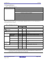
1
E1/E20 Emulator, E2 Emulator Lite Additional Document for User’s Manual (Notes on Connection of RL78) Supported Devices: RL78 Family RL78/D1A, RL78/F12, RL78/F13, RL78/F14, RL78/F1A, RL78/G12, RL78/G13, RL78/G14, RL78/G1A, RL78/G1C, RL78/G1D, RL78/G1E, RL78/G1F, RL78/G1G, RL78/I1A, RL78/I1B, RL78/I1D, RL78/L12, RL78/L13, RL78/L1C All information contained in these materials, including products and product specifications, represents information on the product at the time of publication and is subject to change by Renesas Electronics Corporation without notice. Please review the latest information published by Renesas Electronics Corporation through various means, including the Renesas Electronics Corporation website (http://www.renesas.com). Rev.4.00 Sep 2015 Notice 1. Descriptions of circuits, software and other related information in this document are provided only to illustrate the operation of semiconductor products and application examples. You are fully responsible for the incorporation of these circuits, software, and information in the design of your equipment. Renesas Electronics assumes no responsibility for any losses incurred by you or third parties arising from the use of these circuits, software, or information. 2. Renesas Electronics has used reasonable care in preparing the information included in this document, but Renesas Electronics does not warrant that such information is error free. Renesas Electronics assumes no liability whatsoever for any damages incurred by you resulting from errors in or omissions from the information included herein. 3. Renesas Electronics does not assume any liability for infringement of patents, copyrights, or other intellectual property rights of third parties by or arising from the use of Renesas Electronics products or technical information described in this document. No license, express, implied or otherwise, is granted hereby under any patents, copyrights or other intellectual property rights of Renesas Electronics or others. 4. You should not alter, modify, copy, or otherwise misappropriate any Renesas Electronics product, whether in whole or in part. Renesas Electronics assumes no responsibility for any losses incurred by you or third parties arising from such alteration, modification, copy or otherwise misappropriation of Renesas Electronics product. 5. Renesas Electronics products are classified according to the following two quality grades: “Standard” and “High Quality”. The recommended applications for each Renesas Electronics product depends on the product’s quality grade, as indicated below. “Standard”: Computers; office equipment; communications equipment; test and measurement equipment; audio and visual equipment; home electronic appliances; machine tools; personal electronic equipment; and industrial robots etc. “High Quality”: Transportation equipment (automobiles, trains, ships, etc.); traffic control systems; anti-disaster systems; anticrime systems; and safety equipment etc. Renesas Electronics products are neither intended nor authorized for use in products or systems that may pose a direct threat to human life or bodily injury (artificial life support devices or systems, surgical implantations etc.), or may cause serious property damages (nuclear reactor control systems, military equipment etc.). You must check the quality grade of each Renesas Electronics product before using it in a particular application. You may not use any Renesas Electronics product for any application for which it is not intended. Renesas Electronics shall not be in any way liable for any damages or losses incurred by you or third parties arising from the use of any Renesas Electronics product for which the product is not intended by Renesas Electronics. 6. You should use the Renesas Electronics products described in this document within the range specified by Renesas Electronics, especially with respect to the maximum rating, operating supply voltage range, movement power voltage range, heat radiation characteristics, installation and other product characteristics. Renesas Electronics shall have no liability for malfunctions or damages arising out of the use of Renesas Electronics products beyond such specified ranges. 7. Although Renesas Electronics endeavors to improve the quality and reliability of its products, semiconductor products have specific characteristics such as the occurrence of failure at a certain rate and malfunctions under certain use conditions. Further, Renesas Electronics products are not subject to radiation resistance design. Please be sure to implement safety measures to guard them against the possibility of physical injury, and injury or damage caused by fire in the event of the failure of a Renesas Electronics product, such as safety design for hardware and software including but not limited to redundancy, fire control and malfunction prevention, appropriate treatment for aging degradation or any other appropriate measures. Because the evaluation of microcomputer software alone is very difficult, please evaluate the safety of the final products or systems manufactured by you. 8. Please contact a Renesas Electronics sales office for details as to environmental matters such as the environmental compatibility of each Renesas Electronics product. Please use Renesas Electronics products in compliance with all applicable laws and regulations that regulate the inclusion or use of controlled substances, including without limitation, the EU RoHS Directive. Renesas Electronics assumes no liability for damages or losses occurring as a result of your noncompliance with applicable laws and regulations. 9. Renesas Electronics products and technology may not be used for or incorporated into any products or systems whose manufacture, use, or sale is prohibited under any applicable domestic or foreign laws or regulations. You should not use Renesas Electronics products or technology described in this document for any purpose relating to military applications or use by the military, including but not limited to the development of weapons of mass destruction. When exporting the Renesas Electronics products or technology described in this document, you should comply with the applicable export control laws and regulations and follow the procedures required by such laws and regulations. 10. It is the responsibility of the buyer or distributor of Renesas Electronics products, who distributes, disposes of, or otherwise places the product with a third party, to notify such third party in advance of the contents and conditions set forth in this document, Renesas Electronics assumes no responsibility for any losses incurred by you or third parties as a result of unauthorized use of Renesas Electronics products. 11. This document may not be reproduced or duplicated in any form, in whole or in part, without prior written consent of Renesas Electronics. 12. Please contact a Renesas Electronics sales office if you have any questions regarding the information contained in this document or Renesas Electronics products, or if you have any other inquiries. (Note 1) “Renesas Electronics” as used in this document means Renesas Electronics Corporation and also includes its majorityowned subsidiaries. (Note 2) “Renesas Electronics product(s)” means any product developed or manufactured by or for Renesas Electronics. (2012.4) E1/E20/E2 Lite Contents Contents Page 1. Overview ........................................................................................................................................................ 6 1.1. Overview of E1/E20 Emulator and E2 Emulator Lite .......................................................................... 6 1.2. Note on Using E20 .............................................................................................................................. 6 1.3. Configuration of E1/E20/E2 Lite Manuals ........................................................................................... 7 1.4. Supported Devices .............................................................................................................................. 8 2. Designing the User System ........................................................................................................................... 9 2.1. Connecting the E1/E20/E2 Lite to the User System ........................................................................... 9 2.2. Installing the Connector on the User System ...................................................................................... 9 2.2.1. Connecting the User System Interface Cable to the 14-Pin Connector ..................................................... 9 2.3. Pin Assignments of the Connector on the User System .................................................................... 11 2.3.1. 14-Pin Connector Specifications.............................................................................................................. 11 2.4. Recommended Circuit between the Connector and the MCU .......................................................... 13 2.4.1. Connection between the 14-Pin Connector and the RL78 Family MCUs (Except for the 20-Pin and 24-Pin Versions of the RL78/G12). ......................................................................... 13 2.4.2. Connection between the 14-Pin Connector and the RL78 Family MCUs (Only the 20-Pin and 24-Pin Versions of the RL78/G12). .................................................................................. 14 2.5. Notes on Connection ......................................................................................................................... 15 2.5.1. RESET# Pin ............................................................................................................................................ 15 2.5.2. TOOL0 Pin............................................................................................................................................... 17 2.5.3. GND ........................................................................................................................................................ 18 2.5.4. VDD ......................................................................................................................................................... 18 2.6. Internal Circuits of the Emulator ........................................................................................................ 19 2.6.1. Internal Circuits of the E1 (when the RL78 Family is Connected) ........................................................... 19 2.6.2. Internal Circuits of the E20 (when the RL78 Family is Connected) ......................................................... 20 2.6.3. Internal Circuits of the E2 Lite (when the RL78 Family is Connected) ..................................................... 21 2.7. Notes on Designing the User System ............................................................................................... 22 2.7.1. Isolators for the E1 and E20 .................................................................................................................... 22 2.7.2. Small Connector Conversion Adapter for the E1 ..................................................................................... 22 3. Notes on Usage ........................................................................................................................................... 24 3.1. Turning the Power On/Off.................................................................................................................. 24 3.1.1. When a Separate Power Supply is Used for the User System ................................................................ 24 3.1.2. When Power is Supplied to the User System from the Emulator (E1/E2 Lite Only) ................................ 25 3.2. Power Supply Function of the E1/E2 Lite .......................................................................................... 25 3.3. MCU Resources to be Occupied ....................................................................................................... 26 3.3.1. Securing an Area for the Debugging Monitor Program ............................................................................ 27 3.3.2. Securing a Stack Area for Debugging ...................................................................................................... 28 3.3.3. Setting an On-Chip Debugging Option Byte ............................................................................................ 28 3.3.4. Setting a Security ID ................................................................................................................................ 29 3.4. Reset ................................................................................................................................................. 30 3.4.1. Operation after a Reset ........................................................................................................................... 30 3.4.2. SP Value after a Reset ............................................................................................................................ 30 3.5. Flash Memory .................................................................................................................................... 30 3.5.1. Flash Memory Programming by Self-Programming................................................................................. 30 3.5.2. Operation for Voltages and Flash Operation Modes Not Permitting Flash Memory Rewriting................. 31 3.6. GDIDIS .............................................................................................................................................. 31 3.7. RESET# Multiplexed Pin ................................................................................................................... 31 3.8. MCUs that are Used in Debugging ................................................................................................... 32 3.8.1. Usage in Mass-Production ...................................................................................................................... 32 3.8.2. Standalone Operation .............................................................................................................................. 32 3.9. Final Evaluation of the User Program ............................................................................................... 32 3.10. Debug Functions ............................................................................................................................. 33 3.10.1. Step Execution ...................................................................................................................................... 33 3.10.2. [Go to Here] ........................................................................................................................................... 33 R20UT1994EJ0400 Rev.4.00 Sep 16, 2015 Page 3 of 38 E1/E20/E2 Lite Contents 3.10.3. Debugging in Standby Mode ................................................................................................................. 33 3.10.4. Pseudo-Real-Time RAM Monitor Function or Pseudo-Dynamic Memory Modification Function ........... 33 3.10.5. Start/Stop Functions Facility .................................................................................................................. 34 3.10.6. Emulation of Flash Memory CRC Accumulator Function ....................................................................... 34 3.10.7. Break Function ...................................................................................................................................... 34 3.10.8. Events can be Set and Deleted during User Program Execution .......................................................... 35 3.10.9. Trace Function....................................................................................................................................... 35 3.10.10. Battery Backup Function ..................................................................................................................... 35 R20UT1994EJ0400 Rev.4.00 Sep 16, 2015 Page 4 of 38 E1/E20/E2 Lite Terminology Terminology Some specific words used in this user's manual are defined below. Host machine This means a personal computer used to control the emulator. User system This means a user's application system in which the MCU to be debugged is used. User program This means the program to be debugged. Programming Software In this document, this indicates Renesas Flash Programmer that can be used with the E1, E20, or E2 Lite. "#" at the end of a pin name (signal name) "#" at the end of a pin name (signal name) indicates that the pin (signal) is active low (e.g., RESET#). R20UT1994EJ0400 Rev.4.00 Sep 16, 2015 Page 5 of 38 E1/E20/E2 Lite Overview 1. Overview 1.1. Overview of E1/E20 Emulator and E2 Emulator Lite In this document, we describe ‘E1 Emulator’ as ’E1’, ‘E20 Emulator’ as ’E20’ and ‘E2 Emulator Lite’ as ‘E2 Lite’. The E1, E20, and E2 Lite are on-chip debugging emulators for Renesas' mainstream MCUs. The E1 and E2 Lite are highly affordable development tools providing basic debugging functions. The E20 is a development tool allowing sophisticated debugging through enhanced functions such as tracing and RAM monitoring as well as the basic debugging functions of the E1 and E2 Lite. The E1/E20/E2 Lite can also serve as a Flash Programmer. 1.2. Note on Using E20 To use the large trace function and the real-time RAM monitoring function, which are the primary features of the E20, the target MCU must be equipped with a pin for outputting trace information. The available functions are equivalent to those of the E1/E2 Lite (only the internal trace function in the MCU and memory reference and modification during execution). The power supply function from the E20 is not supported. R20UT1994EJ0400 Rev.4.00 Sep 16, 2015 Page 6 of 38 E1/E20/E2 Lite Overview 1.3. Configuration of E1/E20/E2 Lite Manuals The E1/E20/E2 Lite manuals consist of multiple parts: the E1/E20 Emulator User's Manual, the E2 Emulator Lite User's Manual, and the additional documents for the user's manual for each MCU. Be sure to read each part before using the E1/E20/E2 Lite. (1) E1/E20 Emulator User’s Manual The E1/E20 emulator user’s manual has the following contents: Components of the E1/E20 Hardware specifications of the E1/E20 Connection to the E1/E20 and the host machine and user system (2) E2 Emulator Lite User’s Manual The E2 Emulator Lite user’s manual has the following contents: Components of the E2 Lite Hardware specifications of the E2 Lite Connection to the E2 Lite and the host machine and user system (3) E1/E20 Emulator, E2 Emulator Lite Additional Document for User's Manual (Notes on Connection of RL78) The E1/E20 Emulator, E2 Emulator Lite Additional Document for User's Manual (Notes on Connection of RL78) describes information necessary for hardware design such as connection examples, interface circuits, and notes on using the emulator. (4) User’s manual and help for the emulator debugger The user’s manual and help for the emulator debugger describe the functions of the E1/E20 emulator debugger and the operating instructions. Refer to the following for E1/E20. CS+ Integrated Development Environment User's Manual: RL78 Debug Help for e2 studio RL78 Family CS+ Debugging Using Hot Plug-in Function Refer to the following for E2 Lite. Help for e2 studio When using C-SPY made by IAR Systems, also refer to "IAR C-SPY Hardware Debugger System User Guide issued by IAR Systems" published by IAR Systems. R20UT1994EJ0400 Rev.4.00 Sep 16, 2015 Page 7 of 38 E1/E20/E2 Lite Overview 1.4. Supported Devices Table 1-1 Supported Device List Item Description Target MCUs *2 RL78 Family (RL78-S2 Core) *1 RL78/D1x : RL78/D1A RL78/F1x : RL78/F12 RL78/G1x : RL78/G12,RL78/G13,RL78/G1A,RL78/G1C,RL78/G1D, RL78/G1E, RL78/G1F, RL78/G1G RL78/I1x : RL78/I1A RL78/L1x : RL78/L12,RL78/L13 RL78 Family(RL78-S3 Core) *1 RL78/F1x : RL78/F13,RL78/F14,RL78/F1A RL78/G1x : RL78/G14 RL78/I1x : RL78/I1B,RL78/ID RL78/L1x : RL78/L1C *1 For details on the RL78-S2 core or RL78-S3 core, refer to "RL78 Family User's Manual: Software". *2 When using the RL78/G10, refer to "E1/E20 Emulator Additional Document for User's Manual (Notes on Connecting RL78) (for RL78/G10)". Table 1-2 Debugging Function List Item Type of the RL78 Core RL78-S2 Memory reference or change during program execution Pseudo-real-time RAM monitor(RRM) Description RL78-S3 Supported Supported CPU is used when monitoring Dynamic Memory Modification(DMM) Event Supported 1 points Supported 2 points (max) CPU is used when changing Can be used for hardware break (or trace*1) Break Software break Hardware break Supported Supported Supported Supported 2000 points Commonly used by execution and access Forced break Acquired information Supported Not supported Not supported Not supported Supported Supported *2 Supported *2 Supported *2 Supported Supported Supported Supported Not supported Not supported Supported *3 Not supported Trace Start event End event Performance measurement function Measurement item Performance Hot plug-in Coverage measurement function Notes: Branch source PC information User program execution start and event start User program stop, event completion, and full trace memory Between start and stop of user program execution Resolution 100 μs (max) measurement time 119 hours 18 min 1 Only devices in which the trace function was implemented. 2 The trace function is not supported in an RL78/G14 MCU whose ROM size is 64 Kbytes or less. 3 Only RL78/F13, RL78/F14, and RL78/F1A are supported. R20UT1994EJ0400 Rev.4.00 Sep 16, 2015 Page 8 of 38 E1/E20/E2 Lite Designing the User System 2. Designing the User System 2.1. Connecting the E1/E20/E2 Lite to the User System To connect the E1/E20/E2 Lite to the user system, a connector for the user system interface cable must be mounted on the user system. When designing the user system, read this section of this manual and the hardware manual for the MCU in use. 2.2. Installing the Connector on the User System Table 2-1 shows the recommended connectors for the E1/E20/E2 Lite. Table 2-1 Recommended Connectors Connector 14-pin connector Type Number 7614-6002 2514-6002 Manufacturer 3M Japan Limited 3M Limited Specifications 14-pin straight type (Japan) 14-pin straight type (other countries) * Connection to the 38-pin connector of the E20 is not supported. To use the E20, use the 38-pin to 14pin conversion adapter that comes with the E20 for connection to the 14-pin connector on the user system. 2.2.1. Connecting the User System Interface Cable to the 14-Pin Connector Figure 2-1 shows an example of the connection between a user system interface cable of the 14-pin type and the E1/E2 Lite. Figure 2-2 shows an example of connection between the cable with the 14-pin connector and the E20 via the 38-pin to 14-pin conversion adapter. 14-pin user-system interface cable Pin 2 14-pin connector 7614-6002 or 2514-6002 User system Pin 1 Figure 2-1 Connecting the User System Interface Cable to the 14-Pin Connector of the E1/E2 Lite R20UT1994EJ0400 Rev.4.00 Sep 16, 2015 Page 9 of 38 E1/E20/E2 Lite Designing the User System Figure 2-2 Connecting the User System Interface Cable to the 14-Pin Connector of the E20 Emulator CAUTION Limit to the height on connector periphery: For a case where the R0E000200CKA00 is used for connecting the E20 to a 14-pin connector, do not mount other components with a height of 10 mm or more within 5 mm of the connector on the user system. R20UT1994EJ0400 Rev.4.00 Sep 16, 2015 Page 10 of 38 E1/E20/E2 Lite Designing the User System CAUTION Notes on connector insertion and removal: When connecting or disconnecting the user-system interface cable and the emulator or user system, grasp the connector cover at the end of the cable. Pulling the cable itself will damage the wiring. Also, be aware that the user system interface cable has the direction in which it must be inserted. If the cable is connected in the wrong direction, it may be damaged. Correct example Incorrect example 2.3. Pin Assignments of the Connector on the User System 2.3.1. 14-Pin Connector Specifications Figure 2-3 shows the specifications of the 14-pin connector. Table 2-2 on the following pages shows the pin assignments of the 14-pin connector. Pin 1 mark Connector 25.0 23.0 6 x 2.54 = 15.24 (2.54) Connector (top view) Pin 2 Pin 14 Pin 1 Pin 13 0.45 Pin 1 mark Unit: mm Figure 2-3 Emulator Connector Specifications (14 Pins) R20UT1994EJ0400 Rev.4.00 Sep 16, 2015 Page 11 of 38 E1/E20/E2 Lite Designing the User System Table 2-2 14-Pin Connector Pin Assignments 1 2 3 4 Other than the 20-pin and 24-pin versions of RL78/G12 Signal *1 *2 Direction *3 - R.F.U *6 - GND *4 - R.F.U *6 - R.F.U *6 20-pin and 24-pin versions of RL78/G12 Signal *1 *2 Direction *3 - R.F.U *6 - GND *4 - R.F.U *6 RSTPU Input 5 TOOL0 TOOL0 6 RESET_IN 7 8 9 10 R.F.U VDD EMVDD RESET_OUT *6 11 12 13 R.F.U GND RESET_OUT Pin No 14 *1 *2 *3 *4 *5 *6 *7 I/O Output I/O RESET_IN Output R.F.U VDD EMVDD RESET_OUT *6 *7 *5 - - - Input *7 *5 - - - Input *6 *4 *5 - - Input R.F.U GND RESET_OUT *6 *4 *5 - - Input Note This pin is used to pull up the reset line. (Only when selecting the 20-pin or 24-pin version of the RL78/G12.) This pin is used to transmit command/data to the target device This pin is used to input reset signal from the user system This pin is used to output reset signal to the target device This pin is used to output reset signal to the target device - - GND *4 GND *4 For details on the programming software, refer to http://www.renesas.com/products/tools/flash_prom_programming/ These are the names of the MCU pins at the time the E1/E20/E2 Lite is connected (i.e. during debugging). Input to or output from the user system. Securely connect pins 2, 12, and 14 of the connector to GND of the user system. These pins are used for electrical grounding as well as for monitoring of connection with the user system by the E1/E20/E2 Lite. Securely connect both pin 10 and pin 13. This pin is reserved. Perform the open processing. Connect the drive power of the TOOL0 pin. Please connect VDD when the MCU doesn't have power supplies other than VDD such as EVDD. The E2 Lite only supports a single power supply. If you are using an MCU that requires two or more power supplies with the E2 Lite, use a power supply other than VDD, such as EVDD, which has the same voltage as VDD. R20UT1994EJ0400 Rev.4.00 Sep 16, 2015 Page 12 of 38 E1/E20/E2 Lite Designing the User System 2.4. Recommended Circuit between the Connector and the MCU This section shows recommended circuits for connection between the connector and the MCU when the E1/E20/E2 Lite is in use. For processing of signals, refer to section 2.5, Notes on Connection. 2.4.1. Connection between the 14-Pin Connector and the RL78 Family MCUs (Except for the 20-Pin and 24-Pin Versions of the RL78/G12). Figure 2-4 shows a recommended circuit for connection between the 14-pin connector and the RL78 family MCUs (except for the 20-pin and 24-pin versions of the RL78/G12). 14-pin 2.54-mm pitch connector Note 1 Note 2 VDD 1 kΩ Note 3 RESET_IN Note 3 Reset circuit Note 4 6 10 kΩ RESET_OUT Note 3, Note 7, Note 8 EVDD 10,13 RESET# Note 5 Operation voltage for TOOL0 9 EVDD 1 kΩ TOOL0 Note 5 TOOL0 5 MCU VDD VDD VSS R.F.U 8 2,12,14 Note 6 VDD VSS 1,3,4,7,11 Figure 2-4 Example of Connection between the 14-Pin Connector and the RL78 Family MCUs (Except for the 20-Pin and 24-Pin Versions of RL78/G12). Notes: 1 2 3 4 5 6 7 8 The circuits and resistance values listed are recommended but not guaranteed. Determine the circuit design and resistance values by taking into account the specifications of the target device and noise. For flash programming for mass production, perform sufficient evaluation about whether the specifications of the target device are satisfied. For processing of pins not used by the E1/E20/E2 Lite, refer to the user’s manual of the device. For details on how to handle the RESET# pin, refer to section 2.5, Notes on Connection. The RESET_IN pin is used only in debugging. It is not necessary in flash programming by the programming software. The drive power supply of TOOL0 is different depending on devices. Defer to user’s manual of device. Please connect VDD when the MCU doesn't have power supplies other than VDD such as EVDD. Securely connect pins 2, 12, and 14 of the connection to GND of the user system. These pins are used for electrical grounding as well as for monitoring of connection with the user system by the E1/E20/E2 Lite. Securely connect both pin 10 and pin 13. When you use hot plug-in, install a ceramic capacitor (approx. 0.1 µF) between the RESET# pin and GND in order to suppress a noise to the RESET# pin that would occur when the emulator is connected. R20UT1994EJ0400 Rev.4.00 Sep 16, 2015 Page 13 of 38 E1/E20/E2 Lite Designing the User System 2.4.2. Connection between the 14-Pin Connector and the RL78 Family MCUs (Only the 20-Pin and 24Pin Versions of the RL78/G12). Figure 2-5 shows a recommended circuit for connection between the 14-pin connector and the RL78 family MCUs (only the 20-pin and 24-pin version of the RL78/G12). 14-pin 2.54-mm pitch connector RSTPU Note 3 Note 1 Note 2 4 Note 4 Note 3 RESET_IN Note 3 6 Reset circuit 1 kΩ 470 to 510 Ω RESET_OUT Note 3 Note 6 VDD EVDD 10,13 RESET# VDD VDD 8 9 MCU VDD 1 kΩ TOOL0 VSS R.F.U TOOL0 5 2,12,14 Note 5 VSS 1,3,4,7,11 Figure 2-5 Example of Connection between the 14-Pin Connector and the RL78 Family MCUs (Only the 20-Pin and 24-Pin Versions of the RL78/G12). Notes: 1 2 3 4 5 6 The circuits and resistance values listed are recommended but not guaranteed. Determine the circuit design and resistance values by taking into account the specifications of the target device and noise. For flash programming for mass production, perform sufficient evaluation about whether the specifications of the target device are satisfied. For processing of pins not used by the E1/E20/E2 Lite, refer to the hardware manual for the device. The recommended circuit for the RESET# pin differs depending on whether the multiplexed functions are used. For details on how to handle the RESET# pin, also refer to section 2.5, Notes on Connection. The RESET_IN pin is used only in debugging. It is not necessary in flash programming by the programming software. Securely connect pins 2, 12, and 14 of the connection to GND of the user system. These pins are used for electrical grounding as well as for monitoring of connection with the user system by the E1/E20/E2 Lite. Securely connect both pin 10 and pin 13. R20UT1994EJ0400 Rev.4.00 Sep 16, 2015 Page 14 of 38 E1/E20/E2 Lite Designing the User System 2.5. Notes on Connection Wiring patterns between the connector and the MCU must be as short as possible (within 50 mm is recommended). Do not connect the signal lines between the connector and MCU to other signal lines on the board. For the handling of pins while the E1/E20/E2 Lite is not in use, refer to the hardware manual for the MCU. 2.5.1. RESET# Pin The RESET# pin is used by the E1/E20/E2 Lite to monitor the pin state and issue a reset to the device. Therefore, a reset signal on the user system is once input to the E1/E20/E2 Lite where it is controlled by masking and then output to the target device. Connection examples of the RESET# pin section are shown in Table 2-3 and Figure 2-6 to Figure 2-10. When flash programming by the programming software is to be performed, the RESET# pin should be designed so that the reset signal on the user system does not conflict with the reset signal from the E1/E20/E2 Lite. When you use hot plug-in, install a ceramic capacitor (approx. 0.1 µF) between the RESET# pin and GND in order to suppress a noise to the RESET# pin that would occur when the emulator is connected. Hot plug-ins are not available if there is no reset circuit. Table 2-3 Connection Examples According to the Reset Circuit on the User System No 1 2 3 Target Device 20-pin and 24-pin versions of the RL78/G12 Case There is a reset circuit on the user system. Reference Figure 2-6 There is no reset circuit on the user system. (when using the P125/KR1/SI01 function which is multiplexed with RESET#) Figure 2-7 Other than above There is a reset circuit on the user system. (Resistors are used to switch between usage and non-usage of the emulator) There is a reset circuit on the user system. (A jumper is used to switch between usage and non-usage of the emulator) The power-on reset circuit is the only reset circuit on the user system. Figure 2-8 4 5 R20UT1994EJ0400 Rev.4.00 Sep 16, 2015 Figure 2-9 Figure 2-10 Page 15 of 38 E1/E20/E2 Lite Designing the User System <Connection Example 1 of RESET for the 20-Pin and 24-Pin Versions of the RL78/G12> (Recommended Circuit) 14-pin 2.54-mm pitch connector RSPU Note 2 4 RESET_IN 14-pin 2.54-mm pitch connector 1 kΩ Note 1 <Connection Example 2 of RESET for the 20-Pin and 24-Pin Versions of the RL78/G12> (when using the P125/KR1/SI01 function which is multiplexed with RESET#) RESET_IN 6 Reset circuit 470 to 510 kΩ RSTPU RESET_OUT 6 MCU 4 10,13 RESET# 1 kΩ External circuit MCU RESET_OUT 10,13 RESET# Note 1: It is not necessary in flash programming by the programming software. Note 2: Connection is unnecessary when there is no reset circuit on the user system. Figure 2-6 Connection Example 1 of RESET# (Only the 20-Pin and 24-Pin Versions of the RL78/G12) Figure 2-7 Connection Example 2 of RESET# (Only the 20-Pin and 24-Pin Versions of the RL78/G12) <Connection Example 1 of RESET for Other than the 20-Pin and 24-Pin Versions of the RL78/G12> (Recommended Circuit) VDD R1 1 kΩ 14-pin 2.54-mm pitch connector RESET_IN Note 2 Note 1 Reset circuit 6 Note 1 R2 10 kΩ Note 2 RESET_OUT 10,13 MCU RESET# Note 1: It is not necessary in flash programming by the programming software. Note 2: Make the resistance of at least R1 ten times that of R2, R1 being 10 kΩ or more. Figure 2-8 Connection Example 1 of RESET# (Other than the 20-Pin and 24-Pin Versions of the RL78/G12) <Connection Example 2 of RESET for Other than the 20-Pin and 24-Pin Versions of the RL78/G12> (A jumper is used to switch connection to the E1/E20.) <Connection Example 3 of RESET for Other than the 20-Pin and 24-Pin Versions of the RL78/G12> (The power-on reset circuit is the only reset circuit on the user system) 14-pin 2.54-mm pitch connector 14-pin 2.54-mm pitch connector RESET_IN 6 Reset circuit RESET_IN 6 VDD 1 k to 10 kΩ MCU A RESET_OUT 10,13 RESET_OUT 10,13 MCU RESET# RESET# B C When E1/E20 is connected: B-C shorted When E1/E20 is not connected: A-B shorted Figure 2-9 Connection Example 2 of RESET# Figure 2-10 Connection Example 3 of RESET# (Other than the 20-Pin and 24-Pin Versions of the RL78/G12) (Other than the 20-Pin and 24-Pin Versions of the RL78/G12) ・Do not install capacitors, series resistors, or filters on signal lines; if attempted, correct communication may not be established. ・The circuits and resistance values listed are recommended but not guaranteed. Determine the circuit design and resistance values by taking into account the specifications of the target device and noise. ・Securely connect pins 2, 12, and 14 to GND of the user system. These pins are used for electrical grounding as well as for monitoring of connection with the user system by the E1/E20/E2 Lite. ・Securely connect both pin 10 and pin 13. R20UT1994EJ0400 Rev.4.00 Sep 16, 2015 Page 16 of 38 E1/E20/E2 Lite Designing the User System 2.5.2. TOOL0 Pin The E1/E20/E2 Lite uses the TOOL0 pin. Any functions that are multiplexed on this pin are not available. Pull up the signals of the TOOL0 pin at 1 kΩ and do not arrange these signal lines in parallel with or across other high-speed signal lines. 14-pin 2.54-mm pitch connector Operation voltage for TOOL0 MCU 1 kΩ TOOL0 TOOL0 Figure 2-11 Connection Example of the TOOL0 Pin Do not use adjacent resistors for pull-up of the TCK pin because they may affect or may be affected from other pins. Do not install capacitors, series resistors, or filters on signal lines; if attempted, correct communication may not be established. R20UT1994EJ0400 Rev.4.00 Sep 16, 2015 Page 17 of 38 E1/E20/E2 Lite Designing the User System 2.5.3. GND The pins of the connector marked "GND" must be at the same ground level as the VSS pin of the MCU. 2.5.4. VDD Connect the VDD of the connector to the VDD (power supply) of the user system. Use the emulator within the power supply voltage of 1.8 V to 5.5 V and within the operating voltage range of the MCU. When power is supplied to the user system from other than the emulator, the E1/E20/E2 Lite consumes the power supply for the last output and first input buffers of the emulator. E1: E20: E2 Lite: 3.3 V: approximately 20 mA, 5.0 V: approximately 40 mA 3.3 V: approximately 40 mA, 5.0 V: approximately 100 mA 3.3 V: approximately 20 mA, 5.0 V: approximately 40 mA The E1/E2 Lite can supply power to a simple evaluation system. E1: Can supply power of 3.3 V or 5.0 V, up to 200 mA. E2 Lite: Can supply power of 3.3 V, up to 200 mA. When using the power supply function of the E1/E2 Lite, check the voltage supplied to the user system. Particularly, when the 5.0-V supply option is selected, the voltage may drop 0.5 V or more since it depends on the USB VBUS power-supply voltage. The on-chip debugging circuit in the device operates during on-chip debugging. Therefore current consumption of the device increases. When evaluating current consumption of the device, do not connect the E1/E20/E2 Lite. Power supply from the E1/E2 Lite depends on the quality of the USB power supply of the host machine, and as such, precision is not guaranteed. When writing a program that requires reliability, do not use the power supply function of the E1/E2 Lite. Use a stable, separate power supply for the user system. When writing a program for mass production processes, use the Renesas Flash Programmer. For details on the programming software, refer to: http://www.renesas.com/products/tools/flash_prom_programming/ . WARNING Warning for Turning the Power On/Off: When supplying power, ensure that there are no shorts between VDD and GND. Only connect the E1/E20/E2 Lite after confirming that there are no mismatches of alignment on the user system port connector. Incorrect connection will result in the host machine, the E1/E20/E2 Lite, and the user system emitting smoke or catching fire. R20UT1994EJ0400 Rev.4.00 Sep 16, 2015 Page 18 of 38 E1/E20/E2 Lite Designing the User System 2.6. Internal Circuits of the Emulator 2.6.1. Internal Circuits of the E1 (when the RL78 Family is Connected) Figure 2-12 shows the internal circuits of the E1 with the RL78 family connected. User-side connector Power-supply circuit VDD 8 (only for use in the mode to supply power to the user system) 100 kΩ 3.3 V 100 kΩ × 2 22 Ω 74LVC125 RSTPU 4 100 kΩ 74LVC8T245 EMVDD EMVDD 74LVC125 22 Ω 100 kΩ TOOL0 5 74LVC2T245 22 Ω 74LVC125 RESET_IN 6 74LVC8T245 Emulator control circuit 22 Ω 74LVC125 RESET_OUT 74LVC8T245 10 3.3 V 22 Ω 74LVC125 100 kΩ GND 14 3.3 V 470 Ω EMVDD EMVDD 9 74LVC8T245 74LVC125 22 Ω RESET_OUT Self-recovering fuse 13 GND 2,12 Figure 2-12 Internal Circuit of the E1 (when the RL78 Family is Connected) R20UT1994EJ0400 Rev.4.00 Sep 16, 2015 Page 19 of 38 E1/E20/E2 Lite Designing the User System 2.6.2. Internal Circuits of the E20 (when the RL78 Family is Connected) Figure 2-13 shows the internal circuits of the E20 with the RL78 family connected. User-side connector VDD 8 100 kΩ 3.3 V 100 kΩ × 2 22 Ω 74LVC125 RSTPU 4 100 kΩ 74LVC8T245 EMVDD EMVDD 74LVC125 22 Ω 100 kΩ TOOL0 5 74LVC2T245 22 Ω 74LVC125 RESET_IN 6 74LVC8T245 Emulator control circuit 22 Ω 74LVC125 RESET_OUT 74LVC8T245 10 3.3 V 22 Ω 74LVC125 100 kΩ GND 14 3.3 V 470 Ω EMVDD EMVDD 9 74LVC8T245 74LVC125 22 Ω RESET_OUT Self-recovering fuse 13 GND 2,12 Figure 2-13 Internal Circuits of the E20 (RL78 Family) R20UT1994EJ0400 Rev.4.00 Sep 16, 2015 Page 20 of 38 E1/E20/E2 Lite Designing the User System 2.6.3. Internal Circuits of the E2 Lite (when the RL78 Family is Connected) Figure 2-14 shows the internal circuits of the E2 Lite with the RL78 family connected. User-side connector 100 kΩ × 5 Power-supply circuit VDD 8 (only for use in the mode to supply power to the user system) 3.3 V 1 MΩ 74LVC125 47 Ω RSTPU 4 74LVC8T245 74LVC125 47 Ω TOOL0 5 74LVC8T245 74LVC125 47 Ω RESET_IN 6 74LVC8T245 Emulator control circuit 74LVC125 74LVC8T245 47 Ω RESET_OUT 3.3 V 100 kΩ 47 Ω 74LVC125 10 GND 14 47 Ω EMVDD 9 74LVC8T245 74LVC125 74LVC8T245 47 Ω RESET_OUT Self-recovering fuse 13 GND 2,12 1,3,7,11 Figure 2-14 Internal Circuits of the E2 Lite (when the RL78 Family is Connected) R20UT1994EJ0400 Rev.4.00 Sep 16, 2015 Page 21 of 38 E1/E20/E2 Lite Designing the User System 2.7. Notes on Designing the User System 2.7.1. Isolators for the E1 and E20 For a debugging environment where there is a difference in potential between the GND of the user system and that of the host PC, use the isolator for the E1 emulator (R0E000010ACB20) which is separately available from Renesas. That is, use the isolator for the E1 (R0E000010ACB20) with the E2 Lite in such situations. 2.7.2. Small Connector Conversion Adapter for the E1 A small connector conversion adapter for the E1 (R0E000010CKZ11) is separately available from Renesas for user system boards which are too small to mount the 14-pin connector that is the standard connector for the E1 and E2 Lite. By using the adapter, you can reduce the area taken up by the connector mounted on your system. However, when you use the small connector conversion adapter for the E1, be aware that the pin assignments of the connector differ from those of the standard interface connector for the E1 and E2 Lite. The pin assignments on the 14-pin connector when the small connector conversion adapter for the E1 is used are shown in Table 2-4. The small connector conversion adapter for the E1 can also be used with the E2 Lite. User-system interface cable for E1 (R0E000010KCE00) or E2 Lite (RTE0T0002LKCE00000R) Small connector conversion adapter for the E1 (R0E000010CKZ11) CN1 CN2 Orientation key Pin 1 Pin 13 14-pin connector on the user system (TFM-107-02-L-D(SMT) or TFM-107-01-L-D(DIP)): manufactured by Samtec, Inc. User system Figure 2-15 Usage of the Small Connector Conversion Adapter for the E1 R20UT1994EJ0400 Rev.4.00 Sep 16, 2015 Page 22 of 38 E1/E20/E2 Lite Designing the User System Table 2-4 Connector Pin Assignments when the Small Connector Conversion Adapter for the E1 is Used 1 2 3 4 5 Other than the 20-pin and 24-pin versions of RL78/G12 Signal *1 *2 Direction *3 - GND *4 - R.F.U *6 - VDD - R.F.U *6 RESET_OUT *5 Input 6 7 GND RESET_OUT *4 *5 - Input 8 9 10 R.F.U R.F.U TOOL0 *6 *6 11 R.F.U *6 12 RESET_IN Pin No. 13 14 *1 *2 *3 *4 *5 *6 *7 20-pin and 24-pin versions of RL78/G12 Signal *1 *2 Direction *3 - GND *4 - R.F.U *6 - VDD - R.F.U *6 RESET_OUT *5 Input GND RESET_OUT *4 *5 - Input - - I/O R.F.U R.F.U TOOL0 *6 *6 - - I/O - RSTPU Output RESET_IN Input Output Note This pin is used to output reset signal to the target device This pin is used to output reset signal to the target device This pin is used to transmit command/data to the target device This pin is used to pull up the reset line. (Only when selecting the 20pin and 24-pin version of the RL78/G12.) This pin is used to input reset signal from the user system - - EMVDD *7 EMVDD *7 - - GND *4 GND *4 For details on the programming software, refer to: http://www.renesas.com/products/tools/flash_prom_programming/ These are the names of the MCU pins at the time the E1/E20/E2 Lite is connected (i.e. during debugging). Input to or output from the user system. Securely connect pins 1, 6, and 14 of the connector to GND of the user system. These pins are used for electrical grounding as well as for monitoring of connection with the user system by the E1/E20/E2 Lite. Securely connect both pin 5 and pin 7. This pin is reserved. Perform the open processing. Connect the drive power of the TOOL0 pin. Please connect VDD when the MCU doesn't have power supplies other than VDD such as EVDD. The E2 Lite only supports a single power supply. If you are using an MCU that requires two or more power supplies with the E2 Lite, use a power supply other than VDD, such as EVDD, which has the same voltage as VDD. R20UT1994EJ0400 Rev.4.00 Sep 16, 2015 Page 23 of 38 E1/E20/E2 Lite Designing the User System 3. Notes on Usage 3.1. Turning the Power On/Off Turn the power of the E1/E20/E2 Lite and the user system following the procedure below. 3.1.1. When a Separate Power Supply is Used for the User System <When using the emulator> (1) Check that the power is off. Check that the user system is turned off. When using the E20, check its power switch is off. (2) Connect the user system. Connect the emulator and the user system with a user-system interface cable. (3) Connect the host machine and turn on the emulator. Connect the emulator and the host machine with a USB interface cable. The E1/E2 Lite is turned on by connecting the USB interface cable. When using the E20, turn on its power switch. (4) Launch the emulator debugger or programming software. Launch the emulator debugger or programming software. (5) Turn on the user system. Turn on the user system. (6) Launch the emulator debugger or connect the programming software to the emulator. Connections may vary depending on software. <When finished using the emulator> (1) Close the emulator debugger or disconnect the emulator from the programming software. Disconnections may vary depending on software. (2) Turn off the user system. Turn off the user system. (3) Close the emulator debugger or the programming software. Close the emulator debugger or the programming software. (4) Turn off the emulator and disconnect the emulator. When using the E20, turn off its power switch. Disconnect the USB interface cable from the E1/E2 Lite. The E1/E2 Lite is turned off by disconnecting from the USB interface cable. (5) Disconnect the user system. Disconnect the user system interface cable from the user system. CAUTION Notes on the User System Power Supply: While the power of the user system is on, do not turn off the host machine, unplug the USB interface cable, or turn off the power switch of the E20. The user system may be damaged due to leakages current. R20UT1994EJ0400 Rev.4.00 Sep 16, 2015 Page 24 of 38 E1/E20/E2 Lite Designing the User System 3.1.2. When Power is Supplied to the User System from the Emulator (E1/E2 Lite Only) <When using the emulator> (1) Connect the user system. Connect the emulator and the user system with a user-system interface cable. (2) Connect the host machine and turn on the emulator. Connect the emulator and the host machine with a USB interface cable, then turn on the emulator. (3) Launch the emulator debugger or programming software. Launch the emulator debugger or programming software and select the setting of power supply to the user system. (4) Connect the emulator debugger or programming software to the emulator. Connections may vary depending on software. <When finished using the emulator> (1) Disconnect the emulator debugger or programming software from the emulator. Disconnections may vary depending on software. (2) Close the emulator debugger or programming software. Close the emulator debugger or programming software. (3) Turn off the emulator and disconnect the emulator. Disconnect the USB interface cable from the emulator, then turn off the emulator. (4) Disconnect the user system. Disconnect the user system interface cable from the user system. 3.2. Power Supply Function of the E1/E2 Lite When using the power supply function of the E1/E2 Lite, check that the voltage is supplied to the user system. Particularly, when the 5.0-V supply option is selected, the voltage may drop 0.5 V or more since it depends on the USB VBUS power-supply voltage. Note that the E2 Lite supports power supply of 3.3 V only. When debugging a system with two power supplies (VDD, EVDD, etc.) to the MCU, power cannot be supplied from the E1/E2 Lite. R20UT1994EJ0400 Rev.4.00 Sep 16, 2015 Page 25 of 38 E1/E20/E2 Lite Designing the User System 3.3. MCU Resources to be Occupied Figure 3-1 shows the areas which are occupied by the E1/E20/E2 Lite for debugging. These areas (shaded sections) are used for debugging. These areas should not be changed to save the user program or data. If a change is made, control by the E1/E20/E2 Lite is no longer possible. However, when "No" is selected in the [Permit flash programming] property of the debugger, the internal ROM spaces shown in Figure 3-1 and Figure 3-2 are not used (only the internal RAM spaces are used). When selecting not to permit flash memory rewriting with the debugger's property, also refer to section 3.3.3, Setting of On-Chip Debugging Option Byte, and section 3.5.2, Operation for Voltages and Flash Operation Modes Not Permitting Flash Memory Rewriting. Internal ROM space Internal ROM end address Debug monitor area 256 bytes Internal RAM space Internal RAM end address Stack area for debugging 4 bytes or 12 bytes Debug monitor area 256 bytes 000D8h 000CEh 000C4h 000C3h Debug monitor area 10 bytes Security ID area 10 bytes On-chip debug option byte area 1 byte 00004h 00002h 00000h Debug monitor area 2 bytes Reset vector area 2 bytes Figure 3-1 MCU Resources to be Occupied (E1/E20) Internal ROM end address Internal ROM space Debug monitor area 256 bytes Debug monitor area 256 bytes Internal RAM space Internal RAM end address Stack area for debugging 4 bytes, 8 bytes, or 12 bytes Debug monitor area 256 bytes 000D8h 000CEh 000C4h 000C3h Debug monitor area 10 bytes Security ID area 10 bytes On-chip debug option byte area 1 byte 00004h 00002h 00000h Debug monitor area 2 bytes Reset vector area 2 bytes Figure 3-2 MCU Resources to be Occupied (E2 Lite) R20UT1994EJ0400 Rev.4.00 Sep 16, 2015 Page 26 of 38 E1/E20/E2 Lite *1 Designing the User System The reset vector area is used by the program for the E1/E20/E2 Lite when performing debugging with the E1/E20/E2 Lite. If the contents of the reset vector area are changed, control by the E1/E20/E2 Lite is no longer possible. 3.3.1. Securing an Area for the Debugging Monitor Program You may need to secure the area to which the debugging monitor program is to be allocated. The monitor program initializes the debugger communications interface and handles processing to make the CPU run or break execution. The user program or data must not be placed within 23 bytes of the on-chip debugging option byte, Note1 and leave an area of at least 768 bytes before the address where the internal ROM area ends. In addition, the reset vector must be changed if it points to an address to which the monitor program is allocated. [Securing the area] Specifically securing the area for the monitor program is not necessarily required if the user program does not use the area. However, to avoid problems that may occur while the debugger is starting up, we recommend securing this area in advance by using a build tool or some other means. Note: 1 The required area differs according to the state of usage of the pseudo-RRM/DMM function or the start/stop facility (only the E2 Lite supports the latter). Example (device with 256 Kbytes of on-chip ROM) Pseudo-RRM/DMM function and start/stop function are not in use: Monitor program is located at addresses 0x3FF00 to 0x3FFFF (256 bytes). Pseudo-RRM/DMM function or start/stop function is in use: Monitor program is located at addresses 0x3FE00 to 0x3FFFF (512 bytes). Pseudo-RRM/DMM function and start/stop function are in use: Monitor program is located at addresses 0x3FD00 to 0x3FFFF (768 bytes). R20UT1994EJ0400 Rev.4.00 Sep 16, 2015 Page 27 of 38 E1/E20/E2 Lite Designing the User System 3.3.2. Securing a Stack Area for Debugging The debugger requires 4 bytes as a stack area for debugging except if start/stop functions (only supported by the E2 Lite) are in use, in which case the size of the stack area for debugging is up to 8 bytes. Since this area is allocated immediately below the main stack area, the address of this area varies with increases and decreases in the stack size. That is, if a program is using none of the stack (the stack is empty), the 4- or 8-byte stack area for the debugger remains. Note1 Make sure the stack area for debugging does not go beyond the range of the internal RAM space. Figure 3-3 and Figure 3-4 show examples in which the stack area has increased with the start address of the internal RAM space being 0xFCF00. 0xFFEDF 0xFFEDF 0xFFEDF Stack area Stack area Stack area for debugging 4 bytes or 12 bytes Stack area Stack area for debugging 4 bytes or 12 bytes Available space in internal RAM 0xFCF00 0xFCF00 Available space in internal RAM 0xFCF00 Stack area for debugging 4 bytes or 12 bytes Figure 3-3 Variation of Address of Stack Area for Debugging (E1/E20) 0xFFEDF 0xFFEDF 0xFFEDF Stack area Stack area Stack area for debugging 4 Bytes, 8 bytes, or 12 bytes Stack area Available space in internal RAM 0xFCF00 0xFCF00 Stack area for debugging 4 Bytes, 8 bytes, or 12 bytes Available space in internal RAM 0xFCF00 Stack area for debugging 4 Bytes, 8 bytes, or 12 bytes Figure 3-4 Variation of Address of Stack Area for Debugging (E2 Lite) Note: 1 During self-programming, the size of the stack area for debugging is up to 12 bytes. Refer to the self-programming manual for how to secure the stack area for self programming. The start/stop function is disabled for self-programming, so is irrelevant to the size of the stack area for debugging. 3.3.3. Setting an On-Chip Debugging Option Byte This is the area for the security setting to prevent the flash memory from being read by an unauthorized person. For settable values, refer to the user's manual for each MCU. [Setting an on-chip debugging option byte] *1 Set the on-chip debugging option byte in either of the following ways. (a) Embed the on-chip debugging option byte at address 0xC3 in the user program. Embed the on-chip debugging option byte at address 0xC3 in the user program. (b) Set the on-chip debugging option byte by the build tool. For details on the setting method, refer to the user's manual for the build tool. R20UT1994EJ0400 Rev.4.00 Sep 16, 2015 Page 28 of 38 E1/E20/E2 Lite *1 Designing the User System If the value of the on-chip debugging option byte set in the device disables on-chip debugging (OCDENSET = 0), the debugger cannot be started when "No" is selected in the [Permit flash programming] property of the debugger. If a setting to enable flash programming is made, though the debugger can be started, the flash memory will be in an erased state when the debugger is started. 3.3.4. Setting a Security ID This setting is required to prevent the memory from being read by an unauthorized person. Embed a security ID at addresses 0xC4 to 0xCD in the internal flash memory. The debugger starts only when the security ID that is set during debugger startup and the security ID set at addresses 0xC4 to 0xCD match. If the ID codes do not match, the debugger manipulates the target device in accordance with the value set to the on-chip debug option byte area (refer to the hardware manual for each MCU). If the user has forgotten the security ID to enable debugging, erase the flash memory and set the security ID again. Set the security ID in either of the following ways. When both methods (a) and (b) are carried out at the same time, method (b) has priority. (a) Embed the security ID at addresses 0xC4 to 0xCD in the user program. For example if the security ID is embedded as follows, the security ID set by the debugger Note1,Note2 is ″0123456789ABCDEF1234″ (not case-sensitive). (b) Set the security ID by common options of the build tool. For details on the setting method, refer to the user's manual for the build tool. Table 3-1 Example of Security ID Setting Address Value 0x000C4 0x01 0x000C5 0x23 0x000C6 0x45 0x000C7 0x67 0x000C8 0x89 0x000C9 0xAB 0x000CA 0xCD 0x000CB 0xEF 0x000CC 0x12 0x000CD 0x34 Notes: 1 2 When connecting a debugger to a device for which the security ID has been set, the security ID needs to be entered in the debugger. For details on the authentication method, refer to the user's manual for the debugger in use. "0xFFFFFFFFFFFFFFFFFFFF" which is a setting of only "0xFF" cannot be set. R20UT1994EJ0400 Rev.4.00 Sep 16, 2015 Page 29 of 38 E1/E20/E2 Lite Designing the User System 3.4. Reset 3.4.1. Operation after a Reset After an external pin reset or internal reset, the monitor program performs debug initialization processing. Consequently, the time from reset occurrence until user program execution differs from that in the actual device operation. If “No” is selected in Permit flash programming in property of the debug tool, the time until the user program is executed compared with the time when “Yes” is selected is delayed by several 100 ms. 3.4.2. SP Value after a Reset While debugging with the E1/E20/E2 Lite, the SP value after a reset becomes as follows: When the internal RAM space of the device is 768 bytes or more: FC00h When the internal RAM space of the device is less than 768 bytes: Start address of internal RAM + 0x20 [Example] When the start address of internal RAM is 0xFEF00: 0xEF20 3.5. Flash Memory 3.5.1. Flash Memory Programming by Self-Programming (1) Areas which cannot be rewritten by self programming If a space where the debug monitor program is allocated is rewritten by flash self programming, the debugger can no longer operate normally. This caution also applies to boot swapping for such an area. (2) Break occurring during self programming Though breaks other than a forced break can be generated while self programming is in progress, step execution cannot be performed from where the break occurred. If a forced break occurs during self programming, control by the E1/E20/E2 Lite may not be possible. R20UT1994EJ0400 Rev.4.00 Sep 16, 2015 Page 30 of 38 E1/E20/E2 Lite Designing the User System 3.5.2. Operation for Voltages and Flash Operation Modes Not Permitting Flash Memory Rewriting When a voltage with which rewriting or erasure of flash memory cannot be performed has been selected or flash programming has been disabled with the debugger's property, the following debugger operations that accompany flash memory rewriting will cause an error in the debugger and the operations will be invalidated. Writing to internal flash memory Setting or canceling of software breakpoint Starting execution at the set software breakpoint position Step execution at the set software breakpoint position Step-over execution, Return Out execution Come Here Setting, changing, or canceling of hardware breaks Masking/unmasking of internal reset Switching of peripheral breaks The operating frequency range and operating voltage range are set with the flash operation mode. Correct operation may not be carried out when the operating frequency range or operating voltage range is exceeded. 3.6. GDIDIS The global digital input disable register (GDIDIS) which is used to prevent through-current flowing from the input buffers when the EVDD power supply is turned off (EVDD = 0 V) cannot be used in the E1/E20/E2 Lite. This is because the TOOL0 pin of the EVDD power supply cannot accept input when GDIDIS = 1 (Input to input buffers prohibited.) and so communication with the E1/E20/E2 Lite is broken. 3.7. RESET# Multiplexed Pin In the 20-pin and 24-pin versions of the RL78/G12, the RESET# pin has multiplexed pin functions. Therefore, if the following conditions are all satisfied, control by the E1/E20/E2 Lite is no longer possible. The reset/port multiplexed pin is used as a port (PORTSELB = 0) due to the option byte setting (C1h). The option byte setting (C1h) has been rewritten during a break. "Yes" is selected in the [Mask INTERNAL RESET signal] property of the debugger. R20UT1994EJ0400 Rev.4.00 Sep 16, 2015 Page 31 of 38 E1/E20/E2 Lite Designing the User System 3.8. MCUs that are Used in Debugging 3.8.1. Usage in Mass-Production MCUs that are connected to the E1/E20/E2 Lite and used in debugging are placed under stress by repeated programming of flash memory during emulation. Do not use MCUs that were used in debugging in mass-production for end users. Also, as the E1/E20/E2 Lite program is written to the MCU while debugging, do not save the contents of the MCU Flash memory which were used for debugging nor use them as the ROM data for products. 3.8.2. Standalone Operation After downloading a load module file to the device to for on-chip debugging, do not check the operation of this device without E1/E20/E2 Lite. A device after debugging contains the specific program for on-chip debugging, so it is different from actual operation. 3.9. Final Evaluation of the User Program Before entering the mass-production phase, be sure to perform a final evaluation of the program which is written to a flash ROM by the Renesas Flash Programmer, PG-FP5, etc. Be sure to perform the evaluation singly, without the E1/E20/E2 Lite connected. R20UT1994EJ0400 Rev.4.00 Sep 16, 2015 Page 32 of 38 E1/E20/E2 Lite Designing the User System 3.10. Debug Functions 3.10.1. Step Execution (1) Cautions on using step-in (step execution) The value of some SFRs (special function registers) might remain unchanged while stepping into code. If the values of the SFRs do not change while stepping into code, operate the microcontroller by continuously executing the instructions instead of executing them in steps. Stepping into code: Instructions in the user-created program are executed one by one. Continuous execution: The user-created program is executed from the current PC value. (2) Step-in (step execution) of Division operation (target: device with multiplier and divider/multiplyaccumulator). When the instruction which sets (1) the bit 0 (DIVST) of Multiplication/Division control register (MDUC) is stepped, the division operation is not finished. The step execution of the division operation of C source file is not relevant. (3) Illegal memory access detection When the function to detect illegal memory accesses is enabled (IAWCTL.7 = 1), an internal reset will not occur even when step execution is performed for an instruction that will generate an illegal memory access. 3.10.2. [Go to Here] If [Go to Here] is selected, the software breakpoints and event breakpoints that have been set so far will be temporarily invalidated. 3.10.3. Debugging in Standby Mode The break is an interrupt function of the CPU. Standby mode is released by the break generated by using the following debugging functions. <1> Forced break <2> Step execution of the standby instruction (Stops the user program after execution instruction) <3> Short break generated by the pseudo-RRM function (Break When Readout) <4> Short break generated by the pseudo-DMM function (Break When Write) <5> Short break generated by setting a breakpoint while executing the user program 3.10.4. Pseudo-Real-Time RAM Monitor Function or Pseudo-Dynamic Memory Modification Function Note the following points when using the pseudo-real-time RAM monitor (RMM) function or the pseudoDynamic Memory Modification (DMM) function. • Standby mode (HALT or STOP) may be cancelled during monitoring. • The pseudo-RRM function or the pseudo-DMM function does not operate while the CPU operating clock is stopped. • When the number of monitoring points is numerous, the response of the debugger becomes slow. • Influence of the debugger response becomes small by using a watch panel instead of a memory panel. • When operating on the sub clock, neither the pseudo-RRM function nor the pseudo-DMM function will operate. • Even when the RAM guard function is enabled, memory contents can be rewritten by the pseudo-DMM function. R20UT1994EJ0400 Rev.4.00 Sep 16, 2015 Page 33 of 38 E1/E20/E2 Lite Designing the User System 3.10.5. Start/Stop Functions Facility The E1 and E20 do not have a “start/stop” functions (routines) facility but the E2 Lite does. Note the following points if you intend to use this facility. • Even if the start/stop routines write new values to the CPU registers, the states of the registers are restored at the ends of the routines. • Stepped execution of the start/stop routines is not possible. However, every time stepping over of CALL instructions and so on are internally run, the start/stop routine is enabled. • Breaks cannot be used in start/stop routines. • When execution of a user program starts from an address where a software breakpoint has been set, the instruction at the breakpoint is executed, then the start routine is run. The order of execution is (a), (b), and (c) below. (a) Stepped execution (due to the break) of the instruction where the breakpoint is set (b) Running the start routine (c) Executing instructions of the user program following the first address, where the breakpoint is set (continuous execution except in cases of breakpoints or stepped execution) • When execution of the user program starts from an address at which an event break condition is satisfied, the event does not occur if the start function is disabled, but does occur if the start function is enabled. Stepped-execute the instruction before executing the rest of the user program, or disable the start function if you do not require it. • If you intend to use a stop function, specify a subroutine which returns normally. If the specified subroutine does not return normally, the emulator debugger cannot control execution. To restore control, issue a reset of processing by the debugger. • Hot plug-in is disabled while the start/stop facility is in use. 3.10.6. Emulation of Flash Memory CRC Accumulator Function (1) High-speed CRC (code flash : all area) The operation result of CRC is different from actual result. Because monitor program is arranged and reset vector is rewritten by on-chip debugging. Please check the operation of high-speed CRC by using IECUBE or using device without E1/E20. (2) General-purpose CRC(code flash : specification area) The operation result of CRC at following areas is different from actual result. Because monitor program is arranged and reset vector is rewritten by on-chip debugging. - reset vector area - debugging monitor area - on-chip debugging option byte area - software break setting area 3.10.7. Break Function When "System" is selected in the [Monitor clock] property of the debugger, if a break occurs while operating on the sub clock, the E1/E20/E2 Lite switches the system clock to the main clock. Note the following in such a case. If the external clock (EXCLK) is set as the main clock, when a break occurs with the external clock stopped, an error will occur because the clock cannot be switched. Even if an SFR related to the clock is changed during a break, this change will be set in the device just before the user program is executed. Accordingly, the status flag does not change the moment the SFR is changed. When an SFR is rewritten to change the system clock to the sub clock during a break, though the E1/E20/E2 Lite switches to the sub clock just before the user program is executed, this sometimes results in an error after user program execution due to the oscillation stabilization wait time. In this case, set "User" for [Monitor clock] before debugging. R20UT1994EJ0400 Rev.4.00 Sep 16, 2015 Page 34 of 38 E1/E20/E2 Lite Designing the User System 3.10.8. Events can be Set and Deleted during User Program Execution Events can be set and deleted during user program execution. However, if a pin reset occurs after an event has been set or deleted, the contents of the event that was set or deleted during user program execution will be cleared. 3.10.9. Trace Function When selecting not to permit flash memory rewriting with the debugger's property, the debug monitor area will not be located within 256 bytes below the end address of internal ROM. However, trace data cannot be acquired for this area. 3.10.10. Battery Backup Function Debugging the battery backup function of the RL78/l1B is not supported. R20UT1994EJ0400 Rev.4.00 Sep 16, 2015 Page 35 of 38 E1/E20 Emulator, E2 Emulator Lite Additional Document for User's Manual (Notes on Connection of RL78) Publication Date: Sep 16, 2015 Rev.4.00 Published by: Renesas Electronics Corporation http://www.renesas.com SALES OFFICES Refer to "http://www.renesas.com/" for the latest and detailed information. Renesas Electronics America Inc. 2801 Scott Boulevard Santa Clara, CA 95050-2549, U.S.A. Tel: +1-408-588-6000, Fax: +1-408-588-6130 Renesas Electronics Canada Limited 9251 Yonge Street, Suite 8309 Richmond Hill, Ontario Canada L4C 9T3 Tel: +1-905-237-2004 Renesas Electronics Europe Limited Dukes Meadow, Millboard Road, Bourne End, Buckinghamshire, SL8 5FH, U.K Tel: +44-1628-585-100, Fax: +44-1628-585-900 Renesas Electronics Europe GmbH Arcadiastrasse 10, 40472 Düsseldorf, Germany Tel: +49-211-6503-0, Fax: +49-211-6503-1327 Renesas Electronics (China) Co., Ltd. Room 1709, Quantum Plaza, No.27 ZhiChunLu Haidian District, Beijing 100191, P.R.China Tel: +86-10-8235-1155, Fax: +86-10-8235-7679 Renesas Electronics (Shanghai) Co., Ltd. Unit 301, Tower A, Central Towers, 555 Langao Road, Putuo District, Shanghai, P. R. China 200333 Tel: +86-21-2226-0888, Fax: +86-21-2226-0999 Renesas Electronics Hong Kong Limited Unit 1601-1611, 16/F., Tower 2, Grand Century Place, 193 Prince Edward Road West, Mongkok, Kowloon, Hong Kong Tel: +852-2265-6688, Fax: +852 2886-9022 Renesas Electronics Taiwan Co., Ltd. 13F, No. 363, Fu Shing North Road, Taipei 10543, Taiwan Tel: +886-2-8175-9600, Fax: +886 2-8175-9670 Renesas Electronics Singapore Pte. Ltd. 80 Bendemeer Road, Unit #06-02 Hyflux Innovation Centre, Singapore 339949 Tel: +65-6213-0200, Fax: +65-6213-0300 Renesas Electronics Malaysia Sdn.Bhd. Unit 1207, Block B, Menara Amcorp, Amcorp Trade Centre, No. 18, Jln Persiaran Barat, 46050 Petaling Jaya, Selangor Darul Ehsan, Malaysia Tel: +60-3-7955-9390, Fax: +60-3-7955-9510 Renesas Electronics India Pvt. Ltd. No.777C, 100 Feet Road, HALII Stage, Indiranagar, Bangalore, India Tel: +91-80-67208700, Fax: +91-80-67208777 Renesas Electronics Korea Co., Ltd. 12F., 234 Teheran-ro, Gangnam-Gu, Seoul, 135-080, Korea Tel: +82-2-558-3737, Fax: +82-2-558-5141 © 2015 Renesas Electronics Corporation. All rights reserved. Colophon 4.0 E1/E20 Emulator, E2 Emulator Lite Additional Document for User’s Manual (Notes on Connection of RL78) R20UT1994EJ0400