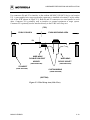
1
M68HC11EVBU/D
REV 3
April 1997
M68HC11EVBU
UNIVERSAL EVALUATION BOARD
USER’S MANUAL
Information contained in this document applies to
REVision (B) M68HC11EVBU Universal Evaluation Boards.
© MOTOROLA Inc. 1990, 1997; All Rights Reserved
Motorola reserves the right to make changes without further notice to any products herein to
improve reliability, function, or design. Motorola does not assume any liability arising out of the
application or use of any product or circuit described herein; neither does it convey any license
under its patent rights nor the rights of others. Motorola products are not designed, intended, or
authorized for use as components in systems intended for surgical implant into the body, or other
application in which the failure of the Motorola product could create a situation where personal
injury or death may occur. Should Buyer purchase or use Motorola products for any such
unintended or unauthorized application, Buyer shall indemnify and hold Motorola and its
officers, employees, subsidiaries, affiliates, and distributors harmless against all claims, costs,
damages, and expenses, and reasonable attorney fees arising out of, directly or indirectly, any
claim of personal injury or death associated with such unintended or unauthorized use, even if
such claim alleges that Motorola was negligent regarding the design or manufacture of the part.
Motorola and the Motorola logo are registered trademarks of Motorola Inc.
Motorola Inc. is an Equal Opportunity/Affirmative Action Employer.
IBM-PC is a registered trademark of International Business Machines Corp.
Apple, MacTerminal, MacWrite are trademarks of Apple Computer, Inc.
Macintosh is a trademark licensed to Apple Computer, Inc.
Macintosh is a trademark of MacIntosh Laboratory, Inc.
Red Ryder is a trademark of Freesoft Company
The computer program stored in the Read Only Memory of the device contains material
copyrighted by Motorola Inc., first published 1990, and may be used only under a license such as
the License For Computer Programs (Article 14) contained in Motorola’s Terms and Conditions
of Sale, Rev. 1/79.
PREFACE
Unless otherwise specified, all address references are in
hexadecimal throughout this manual.
An asterisk (*) following the signal name denotes that the signal is
true or valid when the signal is low.
CONTENTS
CONTENTS
CHAPTER 1 GENERAL INFORMATION
1.1 INTRODUCTION ................................................................................................................. 1-1
1.2 FEATURES ........................................................................................................................... 1-1
1.3 SPECIFICATIONS................................................................................................................ 1-2
1.4 GENERAL DESCRIPTION.................................................................................................. 1-2
1.5 EQUIPMENT REQUIRED ................................................................................................... 1-3
1.6 CUSTOMER SUPPORT ....................................................................................................... 1-4
CHAPTER 2 HARDWARE PREPARATION AND INSTALLATION
2.1 INTRODUCTION ................................................................................................................. 2-1
2.2 UNPACKING INSTRUCTIONS.......................................................................................... 2-1
2.3 HARDWARE PREPARATION............................................................................................ 2-1
2.3.1 Input Power Select Header (J1) .................................................................................... 2-4
2.3.2 Program Execution Select Header (J2)......................................................................... 2-5
2.3.3 MCU Mode Select Headers (J3 and J4) ....................................................................... 2-6
2.3.4 MCU Clock Reconfiguration Headers (J5 and J6) ....................................................... 2-8
2.3.5 Trace Enable Header (J7) ............................................................................................. 2-9
2.3.6 SCI Reconfiguration Headers (J8 and J9)................................................................... 2-10
2.3.7 SPI Reconfiguration Headers (J10 thru J13) .............................................................. 2-11
2.3.8 Real-Time Clock INT* Header (J14) ......................................................................... 2-12
2.3.9 TxD Reconfiguration Header (J15) ............................................................................ 2-13
2.4 REAL-TIME CLOCK, RAM, SERIAL INTERFACE PERIPHERAL............................... 2-14
2.4.1 Diode Jumpers (D1-D4) ............................................................................................. 2-15
2.4.2 Test Points (TP1-TP6) ................................................................................................ 2-16
2.5 WIRE-WRAP AREA .......................................................................................................... 2-17
2.6 INSTALLATION INSTRUCTIONS................................................................................... 2-20
2.6.1 Power Supply – EVBU Interconnection..................................................................... 2-20
2.6.2 Terminal – EVBU Interconnection............................................................................. 2-22
2.6.3 External Equipment – MCU Interconnection ............................................................. 2-25
2.6.4 Wire-Wrap Area – MCU Interconnection .................................................................. 2-25
2.6.5 MCU A/D Converter Circuitry Modifications............................................................ 2-28
M68HC11EVBU/D
v
CONTENTS
CHAPTER 3 MONITOR PROGRAM
3.1 INTRODUCTION ................................................................................................................. 3-1
3.2 PROGRAM DESCRIPTION................................................................................................. 3-1
3.2.1 Initialization.................................................................................................................. 3-1
3.2.2 Command Interpreter.................................................................................................... 3-2
3.2.3 I/O Routines.................................................................................................................. 3-2
3.2.4 Utility Subroutines........................................................................................................ 3-3
3.2.5 Command Table............................................................................................................ 3-5
3.3 INTERRUPT VECTORS ...................................................................................................... 3-5
CHAPTER 4 OPERATING INSTRUCTIONS
4.1 INTRODUCTION ................................................................................................................. 4-1
4.2 CONTROL SWITCH ............................................................................................................ 4-1
4.3 LIMITATIONS...................................................................................................................... 4-1
4.4 OPERATING PROCEDURES.............................................................................................. 4-3
4.4.1 Debugging/Evaluation .................................................................................................. 4-3
4.4.2 Alternate Baud Rates .................................................................................................... 4-3
4.4.3 Monitor Program .......................................................................................................... 4-5
4.5 COMMAND LINE FORMAT .............................................................................................. 4-6
4.6 MONITOR COMMANDS .................................................................................................... 4-7
4.6.1 Assembler/Disassembler............................................................................................. 4-10
4.6.4 Erase All EEPROM Locations ................................................................................... 4-15
4.6.6 Execute Subroutine..................................................................................................... 4-17
4.6.7 Execute Program......................................................................................................... 4-19
4.6.8 Help............................................................................................................................. 4-20
4.6.9 Load S-Records........................................................................................................... 4-21
4.6.10 Memory Display ...................................................................................................... 4-22
4.6.11 Memory Modify....................................................................................................... 4-24
4.6.12 Move Memory .......................................................................................................... 4-26
4.6.13 Proceed/Continue...................................................................................................... 4-27
4.6.14 Register Modify/Display.......................................................................................... 4-28
4.6.15 Stop at Address ........................................................................................................ 4-29
4.6.16 Trace ......................................................................................................................... 4-30
4.6.17 Transparent Mode..................................................................................................... 4-31
4.6.18 Verify........................................................................................................................ 4-32
4.6.19 Transfer Data Bootstrap Mode ................................................................................. 4-33
vi
M68HC11EVBU/D
CONTENTS
CHAPTER 4 OPERATING INSTRUCTIONS
4.7 ASSEMBLY/DISASSEMBLY PROCEDURES ................................................................ 4-35
4.8 DOWNLOADING PROCEDURES.................................................................................... 4-37
4.8.1 Apple Macintosh (with MacTerminal) to EVBU ....................................................... 4-38
4.8.2 Apple Macintosh (with Red Ryder) to EVBU............................................................ 4-40
4.8.3 IBM-PC (with KERMIT) to EVBU............................................................................ 4-41
4.8.4 IBM-PC (with PROCOMM) to EVBU ...................................................................... 4-42
CHAPTER 5 HARDWARE DESCRIPTION
5.1 INTRODUCTION ................................................................................................................. 5-1
5.2 GENERAL DESCRIPTION.................................................................................................. 5-1
5.2.1 Microcontroller ............................................................................................................. 5-1
5.2.2 Memory......................................................................................................................... 5-3
5.2.3 Real-Time Clock + RAM with Serial Interface............................................................ 5-3
5.2.4 Terminal I/O Port Interface........................................................................................... 5-3
CHAPTER 6 SUPPORT INFORMATION
6.1 INTRODUCTION ................................................................................................................. 6-1
6.2 CONNECTOR SIGNAL DESCRIPTIONS .......................................................................... 6-1
6.3 PARTS LIST.......................................................................................................................... 6-6
6.4 DIAGRAMS .......................................................................................................................... 6-8
APPENDIX A
S-RECORD INFORMATION
A-1. INTRODUCTION...................................................................................................................1
A-2 S-RECORD CONTENT...........................................................................................................1
A-3 S-RECORD TYPES .................................................................................................................2
A-4 S-RECORD CREATION .........................................................................................................3
A-5 S-RECORD EXAMPLE ..........................................................................................................3
M68HC11EVBU/D
vii
CONTENTS
LIST OF FIGURES
2-1. EVBU Connector, Switch, and Jumper Header Location Diagram ..................................... 2-3
2-2. Wire-Wrap Area (Top Exploded View)............................................................................. 2-18
2-3. Wire-Wrap Area (Side View)............................................................................................. 2-19
2-4. Terminal I/O Port Connector.............................................................................................. 2-22
2-5. Terminal/Host Computer Cable Assembly Diagram.......................................................... 2-23
2-6. MCU I/O Port Connector P4 (EVBU Top View) .............................................................. 2-26
2-7. MCU I/O Port Connector P5 (EVBU Bottom View)......................................................... 2-27
5-1. EVBU Block Diagram.......................................................................................................... 5-2
6-1. EVBU Parts Location Diagram............................................................................................ 6-8
6-2. EVBU Schematic Diagram (Sheet 1 of 3)............................................................................ 6-9
6-2. EVBU Schematic Diagram (Sheet 2 of 3).......................................................................... 6-11
6-2. EVBU Schematic Diagram (Sheet 3 of 3).......................................................................... 6-13
LIST OF TABLES
1-1. EVBU Specifications ........................................................................................................... 1-2
1-2. External Equipment Requirements....................................................................................... 1-3
2-1. MCU Mode Select................................................................................................................ 2-7
3-1. Utility Subroutine Jump Table ............................................................................................. 3-3
3-2. Interrupt Vector Jump Table ................................................................................................ 3-5
4-1. Monitor Memory Map Limitations ...................................................................................... 4-2
4-2. Monitor Program Commands............................................................................................... 4-8
6-1. Input Power Connector (P1) Pin Assignments..................................................................... 6-1
6-2. Terminal I/O Port Connector (P2) Pin Assignments............................................................ 6-2
6-3. Battery Backup Connector (P3) Pin Assignments................................................................ 6-3
6-4. MCU I/O Port Connectors (P4 and P5) Pin Assignments.................................................... 6-3
6-5. EVBU Parts List................................................................................................................... 6-6
viii
M68HC11EVBU/D
GENERAL INFORMATION
CHAPTER 1
GENERAL INFORMATION
1.1
INTRODUCTION
This manual provides general information, hardware preparation, installation instructions,
monitor program description, operating instructions, hardware description, and support
information for the M68HC11 Universal Evaluation Board (hereafter referred to as EVBU).
Downloading S-record information is contained in Appendix A. While a listing of the EVBU
monitor program is stored on the diskette supplied with the EVBU (see file buf32.asm). (This file
may be viewed using any text reader capable of handling a 102K file.)
1.2
FEATURES
EVBU features include:
•
An economical means of debugging user assembled code and evaluating
MC68HC11A8, E9, 711E9, 811A8, and 811E2 microcontroller unit (MCU) devices
•
One-line assembler/disassembler
•
Host computer downloading capability
•
MC68HC11 MCU based debugging/evaluating circuitry
•
MC68HC68T1 real-time clock + RAM with serial interface peripheral circuitry
•
RS-232C compatible terminal I/O port
•
Wire-wrap area for custom interfacing
•
Single (+5 Vdc) input power source requirements
M68HC11EVBU/D
1-1
GENERAL INFORMATION
1.3
SPECIFICATIONS
Table 1-1 lists the EVBU specifications.
Table 1-1. EVBU Specifications
Characteristics
1.4
Specifications
MCU
MC68HC11E9FN1
Terminal I/O port
RS-232C compatible
Temperature:
Operating
Storage
+25 degrees C
-40 to +85 degrees C
Relative humidity
0 to 90% (non-condensing)
Power requirements:
Primary (P1, Vdd)
Secondary (P1, Vdd) (Optional)
+5.0 Vdc @ 50 mA
+7.5 to +14.0 Vdc @ 50 mA
Battery backup (P3) (Optional)
+3.0 Vdc @ 25 µA
Dimensions:
Width
Length
3.25 in. (8.255 cm)
6.69 in. (16.986 cm)
Wire-wrap Area:
Area
Holes
Approx. 3in. square (7.62 cm)
29 wide x 30 high (one-tenth inch centers)
Standoffs (Optional)
0.75 in. (1.905 cm) or 1.0 in. (2.54 cm)
GENERAL DESCRIPTION
The EVBU provides a low cost tool for debugging/evaluation of MC68HC11A8, E9, 711E9,
811A8, and 811E2 MCUs. The MC68HC11 MCU device is an advanced single-chip MCU with
on-chip memory and peripheral functions. Refer to the MC68HC11 MCU data sheet for
additional device information. The EVBU and a monitor/debugging program called BUFFALO
(Bit User Fast Friendly Aid to Logical Operations) demonstrate the capabilities of this MCU. The
monitor program is contained in MCU ROM. The debugging/evaluation operation lets you debug
user code under control of the BUFFALO monitor program.
1-2
M68HC11EVBU/D
GENERAL INFORMATION
There are two ways to assemble user code: use the line assembler in the BUFFALO monitor
program or assemble code on a host computer and then download the code to the EVBU user
RAM via an Motorola S-records. The monitor program is then used to debug the assembled user
code.
Overall debugging/evaluation control of the EVBU is provided by the monitor program via
terminal interaction. RS-232C terminal I/O port interface circuitry provides communication and
data transfer operations between the EVBU and external terminal/host computer devices. The
terminal I/O port is fixed at 9600 baud.
The EVBU has a wire-wrap area for MCU custom interfacing. The wire-wrap hole pattern lets
you install most standard dual-in-line package (DIP) device wire-wrap sockets, strip sockets,
headers, and connectors. Wire-wrap components can be installed on the topside of the EVBU
printed circuit board (PCB), and wire wrapping can be performed on the bottom side of the PCB.
MCU interfacing is accomplished via the MCU I/O port connector to the wire-wrap area.
EVBU operation requires a user-supplied +5 Vdc power supply and an RS-232C compatible
terminal. You must use an RS-232C compatible host computer to download Motorola S-records
via EVBU terminal I/O port. Download the BUFFALO monitor commands.
The Motorola S-record format was devised for the purpose of encoding programs or data files in
a printable format for transportation between computer systems. Refer to Appendix A for
additional S-record information.
1.5
EQUIPMENT REQUIRED
Table 1-2 lists the external equipment requirements for EVBU operation.
Table 1-2. External Equipment Requirements
External Equipment
+5 Vdc power supply (1)
Terminal (RS-232C compatible)
Host computer (RS-232C compatible) (2)
Terminal/host computer – EVBU RS-232C cable assembly (1)
1. Refer to Chapter 2 for details.
2. Optional – not required for basic operation.
M68HC11EVBU/D
1-3
GENERAL INFORMATION
1.6
CUSTOMER SUPPORT
For information about a Motorola distributor or sales office near you call:
AUSTRALIA, Melbourne – (61-3)887-0711
Sydney – 61(2)906-3855
BRAZIL, Sao Paulo – 55(11)815-4200
CANADA, B. C., Vancouver – (604)606-8502
ONTARIO, Toronto – (416)497-8181
ONTARIO, Ottawa – (613)226-3491
QUEBEC, Montreal – (514)333-3300
JAPAN, Fukuoka – 81-92-725-7583
Gotanda – 81-3-5487-8311
Nagoya – 81-52-232-3500
Osaka – 81-6-305-1802
Sendai – 81-22-268-4333
Takamatsu – 81-878-37-9972
Tokyo – 81-3-3440-3311
CHINA, Beijing – 86-10-68437222
KOREA, Pusan – 82(51)4635-035
Seoul – 82(2)554-5118
DENMARK – (45)43488393
MALAYSIA, Penang – 60(4)2282514
FINLAND, Helsinki – 358-9-6824-400
MEXICO, Mexico City – 52(5)282-0230
Guadalajara – 52(36)21-8977
FRANCE, Paris – 33134 635900
GERMANY,
Langenhagen/Hannover – 49(511)786880
Munich – 49 89 92103-0
Nuremberg – 49 911 96-3190
Sindelfingen – 49 7031 79 710
Wiesbaden – 49 611 973050
HONG KONG, Kwai Fong – 852-6106888
Tai Po – 852-6668333
INDIA, Bangalore – (91-80)5598615
ISRAEL, Herzlia – 972-9-590222
ITALY, Milan – 39(2)82201
PUERTO RICO, San Juan – (809)282-2300
SINGAPORE – (65)4818188
SPAIN, Madrid – 34(1)457-8204
SWEDEN, Solna – 46(8)734-8800
SWITZERLAND, Geneva – 41(22)799 11 11
Zurich – 41(1)730-4074
TAIWAN, Taipei – 886(2)717-7089
THAILAND, Bangkok – 66(2)254-4910
UNITED KINGDOM, Aylesbury – 441(296)395-252
UNITED STATES, Phoenix, AZ – 1-800-441-2447
For a list of the Motorola sales offices and distributors: http://www.mcu.motsps.com/sale_off.html
1-4
M68HC11EVBU/D
HARDWARE PREPARATION AND INSTALLATION
CHAPTER 2
HARDWARE PREPARATION AND INSTALLATION
2.1
INTRODUCTION
This chapter provides unpacking instructions, hardware preparation, and installation instructions
for the EVBU.
2.2
UNPACKING INSTRUCTIONS
NOTE
If upon receipt the shipping carton is damaged, request carrier’s
agent is present during unpacking and inspection of the EVBU.
Unpack EVBU from shipping carton. Refer to packing list and verify that all items are present.
Save packing material for storing or reshipping the EVBU.
2.3
HARDWARE PREPARATION
This paragraph describes the inspection/preparation of EVBU components prior to use. This
description ensures the EVBU components are properly configured before start up.
The EVBU should be inspected and prepared for proper jumper placements. Figure 2-1 illustrates
the EVBU connector, switch, and jumper header locations. Diode jumpers (DJX) and test point
(TPX) locations are also illustrated.
An external +5 Vdc power supply connects to P1 on the EVBU. External terminal/host computer
equipment connects to P2 on the EVBU. An external battery may be connected to P3 on the
EVBU for battery backup purposes. Connectors P4 and P5 are used to connect the EVBU to the
wire-wrap area or other user-supplied equipment.
Switch S1 lets you reset the EVBU.
M68HC11EVBU/D
2-1
HARDWARE PREPARATION AND INSTALLATION
NOTES
The following pages describe the EVBU jumper headers. Jumper
headers consist of feed-thru holes, feed-thru holes with cut-trace
shorts on the printed circuit board (PCB) solder side, and jumper
headers with fabricated jumpers installed as shown in Figure 2-1.
The EVBU (factory configuration) is shown in Figure 2-1. The
EVBU is configured for MC68HC11E9 MCU single-chip mode of
operation.
CAUTION
Depending on the application, you may need to cut the cut-trace
shorts on the PCB solder side. Use extreme care when cutting the
cut-trace shorts to avoid cutting adjacent PCB wiring traces.
Failure to adhere to this CAUTION could result in many hours of
troubleshooting and repair time.
Jumper header locations J1 through J15 provide the following functional capabilities:
2-2
•
Input Power Select (J1)
•
Program Execution Select (J2)
•
MCU Mode Select (J3 and J4)
•
MCU Clock Reconfiguration (J5 and J6)
•
Trace Enable (J7)
•
SCI Reconfiguration (J8 and J9)
•
SPI Reconfiguration (J10 thru J12)
•
Real-Time Clock INT* (J14)
•
TxD Reconfiguration (J15)
M68HC11EVBU/D
HARDWARE PREPARATION AND INSTALLATION
D1
J1
D2
J2
P4
P5
P1
S1
J3
J4
J5
J6
J7
J8
J9
J10
J11
J12
J13
J14
P2
J15
D3
P3
WIRE-WRAP
AREA
TP1
TP2
D4 TP3
TP4
TP5
TP6
DENOTES FABRICATED JUMPER INSTALLED ON JUMPER HEADER.
DENOTES JUMPER HEADER SUPPLIED.
DENOTES CUT-TRACE SHORT ON PCB SOLDER SIDE.
DENOTES FEED-THRU HOLES ONLY.
DENOTES FEED-THRU HOLES ONLY.
Figure 2-1. EVBU Connector, Switch, and Jumper Header Location Diagram
M68HC11EVBU/D
2-3
HARDWARE PREPARATION AND INSTALLATION
2.3.1
Input Power Select Header (J1)
Use jumper header J1 to select the input power to be applied to the EVBU. The EVBU is factoryconfigured and shipped with a fabricated jumper installed on pins 1 and 2 as shown below. In
this configuration, you must supply +5.0 Vdc @ 50 mA to the input power connector P1.
J1
1
+5 VDC
2
Fabricated
Jumper
3
+7.5 to +14.0 VDC
If a +5 Vdc power supply is not available, you can connect an alternate power source (+7.5 to
+14.0 Vdc) to the input power connector P1. To utilize this secondary power source, install an
MC78L05C voltage regulator at location U1 (shown below). After installing the voltage
regulator, move the fabricated jumper on pins 1 and 2 of jumper header J1 to pins 2 and 3.
U1
3
MC78L05C
2
1
(TOP PCB VIEW)
2-4
M68HC11EVBU/D
HARDWARE PREPARATION AND INSTALLATION
2.3.2
Program Execution Select Header (J2)
Use jumper header J2 to select whether the BUFFALO monitor prompt is displayed or if a jump
to internal EEPROM is executed. At reset the monitor checks the logic state of the PE0 line. If
PE0 = 0 (a jumper installed on pins 2 and 3 of jumper header J2) the monitor program is
executed and the prompt displayed. If PE0 = 1 (a jumper is installed on pins 1 and 2 of jumper
header J2) the monitor automatically jumps directly to EEPROM (address location $B600) and
executes user program code without monitor intervention.
The EVBU is factory-configured and shipped with a jumper installed on pins 2 and 3 of jumper
header J2 (BUFFALO monitor program execution, shown below). Reconfigure the EVBU by
moving the jumper to pins 1 and 2 of jumper header J2 if you want to jump directly to EEPROM
address $B600 for user code execution.
J2
1
2
3
EEPROM
(LOGIC 1)
Fabricated Jumper
MONITOR
(LOGIC 0)
If you use the PE0 line for A/D operations, the loading condition introduced by jumper header J2
may not be desired. There are two ways to bypass this potential problem.
1. Jumper header J2 is only required at the trailing edge of reset, so you can remove the
fabricated jumper after reset. Using this method, it is possible that your target system
circuitry might drive the PE0 line to the wrong state during reset.
2. Program the first three EEPROM locations with $7E, $E0, and $0A, respectively.
Next, remove installed jumper from jumper header J2. Independent of the level
present on the PE0 line, the BUFFALO monitor will gain control after a reset
operation.
For additional EEPROM jump operation information, described above, refer to EVBU monitor
program (lines 0162 and 0163) of the listing stored on the EVBU diskette (see file buf32.asm).
M68HC11EVBU/D
2-5
HARDWARE PREPARATION AND INSTALLATION
2.3.3
MCU Mode Select Headers (J3 and J4)
Use jumper headers J3 and J4 to select the MCU operation mode. The EVBU resident
M68HC11E9 MCU device (U3) is factory configured and shipped for single-chip mode of
operation. No fabricated jumpers are required on jumper headers J3 and J4 for this configuration
due to the cut-trace short on PCB solder side of J4.
If the J4 cut trace short is cut, you must install a user-supplied fabricated jumper on jumper
header J4 to return the EVBU to the factory configuration (single-chip mode). Jumper header J3
does not contain a cut trace short.
1
2
J3
MODB
J4
MODA
1
2
Cut-Trace Short
NOTE
If J4 cut-trace short is cut, you must install a user-supplied
fabricated jumper on J4 to return it to the factory configuration.
2-6
M68HC11EVBU/D
HARDWARE PREPARATION AND INSTALLATION
In order to select the expanded-multiplexed, special-bootstrap, or special-test modes of operation,
remove the cut-trace short between pins 1 and 2 of jumper header J4,. Then install user-supplied
fabricated jumpers on jumper headers J3 and J4. Refer to Table 2-1 for directions when
configuring the desired EVBU M68HC11E9 MCU mode of operation.
Table 2-1. MCU Mode Select
J4 – MODA (1)
J3 – MODB
Installed (2)
Removed
Single-Chip
Removed (3)
Removed
Expanded-Multiplexed
Installed (2)
Installed
Special-Bootstrap
Removed (3)
Installed
Special-Test
MCU Mode Select
NOTES
1. Installed jumper equals a logic 0 (shorted to ground), while a missing
jumper equals a logic 1 (open/pull-up).
2. The cut-trace short is present or a jumper is installed on J4.
3. The cut-trace short and jumper are removed from J4.
The EVBU can be reconfigured for either the single-chip, expanded-multiplexed, specialbootstrap, or special-test modes of operation via jumper headers J3 and J4. For expandedmultiplexed and special-test modes of operation, additional peripheral circuitry must be
implemented on the EVBU wire-wrap area to support the expanded modes. The EVBU can be
reconfigured for the special-bootstrap mode of operation without additional peripheral circuitry.
M68HC11EVBU/D
2-7
HARDWARE PREPARATION AND INSTALLATION
2.3.4
MCU Clock Reconfiguration Headers (J5 and J6)
Use jumper headers J5 and J6 to connect the MCU EXTAL and XTAL signals (pins 7 and 8) to
the MCU I/O port connectors P4 and P5. This configuration is for remote applications. The
EVBU is factory configured and shipped without installed fabricated jumpers (shown below).
1
2
J5
EXTAL
J6
XTAL
1
2
NOTE
Care should be taken when routing the EXTAL and XTAL signals
to a target system environment and/or EVBU wire-wrap area.
Additional capacitance and/or extra noise could render the resident
MCU oscillator non functional.
For special applications using the MCU EXTAL and XTAL signals in a target system
environment or EVBU wire-wrap area, install fabricated jumpers on jumper headers J5 and J6.
When jumpers are installed, both EXTAL and XTAL signals are routed to the MCU I/O port
connectors P4 and P5.
2-8
M68HC11EVBU/D
HARDWARE PREPARATION AND INSTALLATION
2.3.5
Trace Enable Header (J7)
Use jumper header J7 to select BUFFALO monitor debug operations by connecting the
PA3/OC5 signal (pin 2) to the XIRQ* signal (pin 1). The EVBU is factory-configured and
shipped with a fabricated jumper installed on pins 1 and 2 as shown below. This jumper must be
installed during debugging operations.
J7
XIRQ*
PA3/OC5
1
2
Fabricated Jumper
For special applications which use the PA3/OC5 signal, remove the fabricated jumper on pins 1
and 2 to avoid interference between the PA3/OC5 signal and the XIRQ* signal. In this
configuration, several BUFFALO monitor commands are not available. BUFFALO commands
which will not function without a jumper installed on J7 are: proceed (P), stop at address
(STOPAT), and trace (T) commands.
Refer to the schematic diagram (Figure 6-2) located in Chapter 6 for PA3/OC5 signal wiring
information.
M68HC11EVBU/D
2-9
HARDWARE PREPARATION AND INSTALLATION
2.3.6
SCI Reconfiguration Headers (J8 and J9)
Use jumper headers J8 and J9 (shown below) to connect the MCU PD0/RXD and PD1/TXD
serial communications interface (SCI) signal lines to the MC145407 RS-232C driver/receiver
device (located at U4). Jumper headers J8 and J9 have feed-thru holes with cut-trace shorts.
Fabricated jumpers for jumper headers J8 and J9 are not supplied by the factory.
1
2
J8
PD0/RXD
J9
PD1/TXD
1
2
Cut-Trace Shorts
NOTE
If J8 and J9 cut-trace shorts are cut, you must install user-supplied
fabricated jumpers on J8 and J9 to return them to the factory
configuration.
When isolation of the PD0/RXD and PD1/TXD signal lines (from the MCU SCI to the
MC145407 RS-232C driver/receiver device) are required, you must cut the cut-trace shorts. To
return jumper headers J8 and J9 to the factory configuration install user supplied fabricated
jumpers on the J8 and J9. Refer to the schematic diagram (Figure 6-2) located in Chapter 6 for
PD0/RXD and PD1/TXD signal wiring information.
2-10
M68HC11EVBU/D
HARDWARE PREPARATION AND INSTALLATION
2.3.7
SPI Reconfiguration Headers (J10 thru J13)
Use jumper headers J10 through J13 (shown below) to connect the MCU PD4/SCK, PD2/MISO,
PD3/MOSI, and PD5/SS serial peripheral interface (SPI) signal lines to the MC68HC68T1
peripheral device (location U5). The feed-thru holes for jumper headers J10 through J13 have
cut-trace shorts. Fabricated jumpers for jumper headers J10 through J13 are not supplied by the
factory.
1
2
J10
PD2/MISO
J11
PD3/MOSI
J12
PD4/SCK
J13
PD5/SS
Cut-Trace Shorts
NOTE
If J10 through J13 cut-trace shorts are removed, you must install
user-supplied fabricated jumpers on J10 through J13 to return them
to the factory configuration.
When isolation of the PD4/SCK, PD2/MISO, PD3/MOSI, and PD5/SS signal lines (from the
MCU SPI to the MC68HC68T1 peripheral device) are required, cut the solder-side traces. To
return J10 through J13 to the factory configuration install user supplied fabricated jumpers on
jumper headers J10 through J13. Refer to the schematic diagram (Figure 6-2) located in Chapter
6 for PD4/SCK, PD2/MISO, PD3/MOSI, and PD5/SS signal wiring information.
M68HC11EVBU/D
2-11
HARDWARE PREPARATION AND INSTALLATION
2.3.8
Real-Time Clock INT* Header (J14)
Use jumper header J14 (shown below) to disconnect the MCU XIRQ* signal line from the
MC68HC68T1 peripheral device (located at U5) INT* signal pin. The EVBU is factory
configured and shipped without a fabricated jumper installed on pins 1 and 2 as shown below.
Jumper header J14 is used to connect the INT* output of the MC68HC68T1 peripheral device to
the MCU XIRQ* signal line.
J14
INT*
XIRQ*
1
2
NOTE
The INT* signal line is a output signal which is connected to the
XIRQ* input of the MCU. XIRQ* is also used by the BUFFALO
monitor for tracing (refer to paragraph 2.3.5). Refer to the jumper
header J7 and jumper header J14 descriptions because the
respective functions could interfere with each other.
When connection of the MC68HC68T1 peripheral device INT* signal line to the MCU is
required, you must install a (user supplied) fabricated jumper on the component side of the PCB.
Refer to the schematic diagram (Figure 6-2) located in Chapter 6 for INT* and XIRQ* signal
wiring information.
2-12
M68HC11EVBU/D
HARDWARE PREPARATION AND INSTALLATION
2.3.9
TxD Reconfiguration Header (J15)
As shipped, jumper header J15 (shown below) is used to connect the MC145407 RS-232C
driver/receiver device (located at U4) TxD signal line to the terminal port connector P2. No
jumper header is installed in location J15, it consists of two feed-thru holes with a cut-trace short.
When the cut trace is cut, a user connection is made to J15 pin 2 to facilitate driving a buffered
TxD signal to a user system in the special-bootstrap mode (with the XBOOT command) without
the removal of the external terminal connected to the EVBU terminal port connector P2.
J15
TxD
1
2
NOTE
If J15 cut-trace short is cut, you may solder a grounding strap
between the feed-through-holes on J15 to return it to the factory
configuration.
When the TxD signal line is required for an external connection, you must cut the solder-side
trace and make the connection to J15 pin 2. When reconfiguration of the TxD signal line is
required, you must solder a user-supplied jumper header in the J15 feed-through-holes and then
install a fabricated jumper on the jumper header. Refer to the parts list contained in Chapter 6 for
jumper header J15 component description. Refer to the schematic diagram (Figure 6-2) located in
Chapter 6 for TxD signal wiring information.
M68HC11EVBU/D
2-13
HARDWARE PREPARATION AND INSTALLATION
2.4
REAL-TIME CLOCK, RAM, SERIAL INTERFACE PERIPHERAL
A user-supplied HCMOS real-time clock, RAM, and serial interface peripheral device
(MC68HC68T1) can be installed on the EVBU at location U5. The MC68HC68T1 peripheral
device contains a real-time clock/calendar, a 32 x 8 static RAM, and a synchronous, serial, three
wire interface for MCU communications. Operating in a burst mode, successive clock or RAM
locations can be read or written using only a single starting address An on-chip oscillator allows
acceptance of a selectable crystal frequency or the device can be programmed to accept a 50/60
Hz line input frequency.
Features of the MC68HC68T1 peripheral device are as follows:
•
Full clock features – seconds, minutes, hours (AM/PM), day-of-week, date, month,
year (0-99), auto leap year
•
32 word by 8-bit RAM
•
Direct interface to Motorola serial peripheral interface (SPI)
•
Minimum time-keeping voltage 2.2 V
•
Burst mode for reading/writing successive addresses in clock or RAM
•
Selectable crystal or 50/60 Hz line input
•
Binary-coded-decimal (BCD) data contained in registers
•
Buffered clock output for driving CPU clock, timer, colon, or liquid crystal display
(LCD) backplane
•
Power-on reset with first-time-up flag
•
Freeze circuit eliminates software overhead during a clock read
•
Three independent interrupt modes – alarm, periodic, or power-down sense
•
CPU reset output – provides orderly power up/down
•
Watchdog circuit
Refer to the MC68HC68T1 Real-Time Clock plus RAM with Serial Interface data sheet
(MC68HC68T1/D) for additional device information.
In addition to the MC68HC68T1 circuitry, diode jumpers (D1-D4) and test points (TP1-TP6) are
also included. The following paragraphs describes the purposes of the diode jumpers and test
points in conjunction with the MC68HC68T1 device installed in socket location U5.
2-14
M68HC11EVBU/D
HARDWARE PREPARATION AND INSTALLATION
2.4.1
Diode Jumpers (D1-D4)
Diode jumpers D1-D4 (shown below) are provided on the EVBU for the real-time clock battery
backup operations. The diode jumpers (D1), (D2), and (D3) consist of feed-thru holes with cut
traces on the PCB solder side. Diode jumper D4 feed-thru holes do not include a cut trace.
1
1
1
1
2
2
2
2
1
1
2
D1
D2
D3
D4
2
If the MC68HC68T1 real-time clock battery backup feature is required, you must cut the D1-D3
feed-thru hole cut traces on the PCB solder side, and install the following user-supplied
components on the PCB component side as follows:
D1
1N4001 diode
D2
1N4148 diode
D3
1N4148 diode
D4
1N4148 diode, jumper wire, or resistor (application dependent)
A user-supplied +3.0 Vdc @ 25 µA battery is connected to the EVBU battery connector P3
(feed-thru holes designated + and -) for battery backup purposes as shown below.
P3
+
M68HC11EVBU/D
-
2-15
HARDWARE PREPARATION AND INSTALLATION
The type of battery selected for connector P3 will affect the choice of the component (diode,
jumper wire, or resistor) that will be installed in location D4. Refer to the MC68HC68T1 data
sheet and battery manufacturer recommendations for additional details. Refer to the parts list
contained in Chapter 6 for the battery connector P3 and diode jumpers D1-D4 component
descriptions.
2.4.2
Test Points (TP1-TP6)
Test points TP1-TP6 (shown below) are provided for the user-supplied MC68HC68T1 device
installed in socket location U5. These test point consists of six feed-thru holes. If desired, you
can install a single pin header post (Aptronics # 929705-01-01) in each feed-thru hole.
TP1
CLK OUT = Clock Output
TP2
CPUR* = CPU Reset
TP3
VSYS = System Voltage
TP4
LINE = Line Sense
TP5
POR* = Power-On Reset
TP6
PSE = Power Supply Enable
The above test points are provided for user monitoring and wire-wrap area application purposes
for the MC68HC68T1 device. Refer to the MC68HC68T1 Real-Time Clock plus RAM with
Serial Interface data sheet (MC68HC68T1/D) for additional device information pertaining to the
above test point signals. Refer to the parts list contained in Chapter 6 for test points TP1-TP6
component descriptions.
2-16
M68HC11EVBU/D
HARDWARE PREPARATION AND INSTALLATION
2.5
WIRE-WRAP AREA
The EVBU provides a small wire-wrap area for MCU custom interfacing. The wire-wrap area is
approximately 3.0 inches square, consisting of 29 holes wide by 30 holes high. The holes are on
one-tenth inch centers. Figure 2-2 illustrates an exploded view of the wire-wrap area. A ground
(GND) bus strip resides on the outside parameter of the wire-wrap area. A +5 Vdc bus is also
provided at the upper left end of the wire-wrap area.
With the wire-wrap hole pattern provided, dual-in-line package (DIP) device wire-wrap sockets,
strip sockets, headers, and connectors can be installed. Wire-wrap components can be installed
on the top side of the EVBU, and wire wrapping can be performed on the bottom side of the
EVBU. The use of three-quarter or one inch standoffs are recommended for wire-wrap pin
clearance on the bottom side of the EVBU. The standoff mounting holes are shown below.
P4
P5
WIRE-WRAP
P2
AREA
Two 60-pin MCU I/O port connectors P4 and P5 are provided on the EVBU. Connector P4 is
factory supplied and connector P5 is user supplied. Refer to the parts list contained in Chapter 6
for connector P5 component description. As shown on the following page, connector P5 supplies
the EVBU wire-wrap area with the +5 Vdc and ground (GND) power connections.
M68HC11EVBU/D
2-17
HARDWARE PREPARATION AND INSTALLATION
P5
60
59
29 HOLES
+5 VDC
BUS
30
HOLES
2
1
GROUND (GND) BUS
Figure 2-2. Wire-Wrap Area (Top Exploded View)
2-18
M68HC11EVBU/D
HARDWARE PREPARATION AND INSTALLATION
Use connectors P4 and P5 to interface to the resident MC68HC11E9 MCU device (at location
U3). A user-supplied wire-wrap type header (connector) is installed at location P5 on the solder
side of the PCB (shown in Figure 2-3). Both P4 and P5 connectors are wired parallel to each
other. Connector P4 is primarily used to interface to external equipment or target system.
Connector P5 is primarily used to interface directly to the EVBU wire-wrap area.
(TOP)
EVBU PCB AREA
EVBU WIRE-WRAP AREA
P4
P5
WIRE-WRAP
DOUBLE ROW POST
WIRE-WRAP
DEVICE SOCKET
HEADER
(USER SUPPLIED)
(USER SUPPLIED)
STANDOFF
CUSTOM WIRING
(USER SUPPLIED)
(USER SUPPLIED)
(BOTTOM)
Figure 2-3. Wire-Wrap Area (Side View)
M68HC11EVBU/D
2-19
HARDWARE PREPARATION AND INSTALLATION
2.6
INSTALLATION INSTRUCTIONS
The EVBU is designed for table top operation. A user-supplied +5 Vdc power supply and RS232C compatible terminal are required for EVBU operation. An RS-232C compatible host
computer is optional for downloading user assembled code to the EVBU via the terminal I/O port
connector P2.
2.6.1
Power Supply – EVBU Interconnection
The EVBU requires +5 Vdc @ 50 mA and GND for operation. Interconnection of the power
supply wiring to the EVBU power supply connector P1 is shown below.
The power supply cable consists of two 14-22 AWG wires that interconnect +5 Vdc and ground
(GND) from the user-supplied power supply to the EVBU connector P1.
2-20
M68HC11EVBU/D
HARDWARE PREPARATION AND INSTALLATION
Jumper header J1 is used to select the input power to be applied to the EVBU. The EVBU is
factory-configured and shipped with the fabricated jumper installed on pins 1 and 2 as shown
below. In this configuration, you must supply +5.0 Vdc @ 50 mA (max) to the input power
connector P1.
J1
1
+5 Vdc
Fabricated Jumper
2
3
+7.5 to +14.0 Vdc
If a +5 Vdc power supply is not available, an alternate power source (+7.5 to +14.0 Vdc) can be
connected to the input power connector P1. To utilize this secondary power source, install an
MC78L05C voltage regulator at location U1. Upon completion of the voltage regulator
installation, you must reinstall the fabricated jumper on jumper header J1, from pins 1 and 2 to
pins 2 and 3.
M68HC11EVBU/D
2-21
HARDWARE PREPARATION AND INSTALLATION
2.6.2
Terminal – EVBU Interconnection
Interconnection of an RS-232C compatible terminal to the EVBU is accomplished via a usersupplied cable assembly as shown in Figure 2-5. Connect one end of the cable assembly to
EVBU connector P2 (shown in Figure 2-4). Connect the other end of the cable assembly to the
user-supplied terminal/host computer. Refer to Chapter 6 for connector pin assignments and
signal descriptions of EVBU terminal port connector P2.
For those using an IBM-PC or Apple Macintosh personal computer (PC), use a Hayescompatible-modem cable to connect the PC to EVBU terminal port connector P2.
P2
GND
1
TXD
2
RXD
3
NC
4
CTS
5
DSR
6
SIG-GND
7
DCD
8
NC
9
NC
10
NC
11
NC
12
NC
13
14
NC
15
NC
16
NC
17
NC
18
NC
19
NC
20
DTR
21
NC
22
NC
23
NC
24
NC
25
NC
Figure 2-4. Terminal I/O Port Connector
Figure 2-5 illustrates a suitable cable assembly for connecting the EVBU to a dumb terminal.
This cable assembly is made from standard mass termination ribbon cable components.
2-22
M68HC11EVBU/D
HARDWARE PREPARATION AND INSTALLATION
20 OR 25 CONDUCTOR
FLAT RIBBON
CABLE
3M #3365-20
OR
3M #3365-25
25 "D" SUBMINIATURE
MALE(PIN)
CONNECTORPART #’S:
25 "D" SUBMINIATURE
FEMALE(SOCKET)
CONNECTORPART #’S:
1. CIRCUIT ASSEMBLY CORP
#CA•25•SMD•P
1. CIRCUIT ASSEMBLY CORP
#CA•25•SMD•S
2. ITT CANNON #DBSP-B25P
2. ITT CANNON #DBSP-B25S
3. ANSLEY #609•25P
3. ANSLEY #609•25S
4. WINCHESTER #49•1125P
4. WINCHESTER #49•1125S
25 PIN "D" SUBMINIATURE CONNECTOR
1
2
14
3
15
4
16
5
17
6
18
7
19
8
20
9
21
10
22
11
23
12
24
13
25
1
2
14
3
15
4
16
5
17
6
18
7
19
DCD
NOT CONNECTED
DTR
SIGNAL GND
DSR
CTS
RTS
RXD
TXD
RED WIRE
8
20
9
21
10
22
11
23
12
24
13
25
25 PIN "D" SUBMINIATURE CONNECTOR
Figure 2-5. Terminal/Host Computer Cable Assembly Diagram
M68HC11EVBU/D
2-23
HARDWARE PREPARATION AND INSTALLATION
A Hayes compatible modem cable, purchased from your local computer store, can be used to
connect the EVBU to your host computer.
The EVBU is wired as data communication equipment (DCE) whereas a dumb terminal and most
serial modem ports on host computers are wired as data terminal equipment (DTE). This should
allow a straight-through cable to be used in most setups.
If an unknown cable is used to connect the EVBU to a host computer, a null modem adapter
(shown below) may be required to match the cable to the EVBU terminal port connector.
A null modem adapter is used to reverse the roles of various data and control signals to make a
DTE device appear as a DCE device or vice versa.
DB-25S
DB-25P
GND
1
1
GND
TXD
2
2
TXD
RXD
3
3
RXD
RTS
4
4
RTS
CTS
5
5
CTS
DSR
6
6
DSR
7
7
SIG-GND
DCD
8
8
DCD
DTR
20
20
DTR
SIG-GND
NULL MODEM ADAPTER
2-24
M68HC11EVBU/D
HARDWARE PREPARATION AND INSTALLATION
2.6.3
External Equipment – MCU Interconnection
External equipment to MCU interconnection is accomplished via the EVBU MCU I/O port
connector P4. Connector P4 is supplied by the factory. This connector is mounted on the top side
of the EVBU PCB (shown in Figure 2-3). Connector P4 (shown in Figure 2-6) is a 60-pin header
that facilitates the interconnection of the EVBU MCU circuitry to external equipment or target
system equipment.
For connector pin assignments and signal descriptions of the EVBU MCU I/O port connector P4,
refer to Chapter 6.
2.6.4
Wire-Wrap Area – MCU Interconnection
Wire-wrap area to MCU interconnection is accomplished via the EVBU MCU I/O port connector
P5. Connector P5 is supplied by the user. This connector is mounted on the bottom side of the
EVBU PCB (shown in Figure 2-6). Connector P5 (shown in Figure 2-7) is a 60-pin header that
facilitates the interconnection of the EVBU MCU circuitry to the EVBU wire-wrap area
components.
For connector pin assignments and signal descriptions of the EVBU MCU I/O port connector P5,
refer to Chapter 6. Refer to the parts list contained in Chapter 6 for the connector P5 component
description.
M68HC11EVBU/D
2-25
HARDWARE PREPARATION AND INSTALLATION
P4
GND
60
l
l
59
GND
VCC
58
l
l
57
VCC
SPARE
56
l
l
55
SPARE
SPARE
54
l
l
53
SPARE
VRH
52
l
l
51
VRL
PE7
50
l
l
49
PE3
PE6
48
l
l
47
PE2
PE5
46
l
l
45
PE1
PE4
44
l
l
43
PE0
PB0 / A8
42
l
l
41
PB1 / A9
PB2 / A10
40
l
l
39
PB3 / A11
PB4 / A12
38
l
l
37
PB5 / A13
PB6 / A14
36
l
l
35
PB7 / A15
PA0 / IC3
34
l
l
33
PA1 / IC2
PA2 / IC1
32
l
l
31
PA3 / OC5
PA4 / OC4
30
l
l
29
PA5 / OC3
PA6 / OC2
28
l
l
27
PA7 / OC1
NC
26
l
l
25
PD5 / SS*
PD4 / SCK
24
l
l
23
PD3 / MOSI
PD2 / MISO
22
l
l
21
PD1 / TXD
PD0 / RXD
20
l
l
19
IRQ*
XIRQ*
18
l
l
17
RESET*
PC7 / AD7
16
l
l
15
PC6 / AD6
PC5 / AD5
14
l
l
13
PC4 / AD4
PC3 / AD3
12
l
l
11
PC2 / AD2
PC1 / AD1
10
l
l
9
PC0 / AD0
XTAL
8
l
l
7
EXTAL
STRB / R/W*
6
l
l
5
E
STRA / AS
4
l
l
3
MODA / LIR*
MODB / VSTBY
2
l
l
1
GND
Figure 2-6. MCU I/O Port Connector P4 (EVBU Top View)
2-26
M68HC11EVBU/D
HARDWARE PREPARATION AND INSTALLATION
P5
MODB / VSTBY
2
l
l
1
GND
STRA / AS
4
l
l
3
MODA / LIR*
STRB / R/W*
6
l
l
5
E
XTAL
8
l
l
7
EXTAL
PC1 / AD1
10
l
l
9
PC0 / AD0
PC3 / AD3
12
l
l
11
PC2 / AD2
PC5 / AD5
14
l
l
13
PC4 / AD4
PC7 / AD7
16
l
l
15
PC6 / AD6
XIRQ*
18
l
l
17
RESET*
PD0 / RXD
20
l
l
19
IRQ*
PD2 / MISO
22
l
l
21
PD1 / TXD
PD4 / SCK
24
l
l
23
PD3 / MOSI
NC
26
l
l
25
PD5 / SS*
PA6 / OC2
28
l
l
27
PA7 / OC1
PA4 / OC4
30
l
l
29
PA5 / OC3
PA2 / IC1
32
l
l
31
PA3 / OC5
PA0 / IC3
34
l
l
33
PA1 / IC2
PB6 / A14
36
l
l
35
PB7 / A15
PB4 / A12
38
l
l
37
PB5 / A13
PB2 / A10
40
l
l
39
PB3 / A11
PB0 / A8
42
l
l
41
PB1 / A9
PE4
44
l
l
43
PE0
PE5
46
l
l
45
PE1
PE6
48
l
l
47
PE2
PE7
50
l
l
49
PE3
VRH
52
l
l
51
VRL
SPARE
54
l
l
53
SPARE
SPARE
56
l
l
55
SPARE
VCC
58
l
l
57
VCC
GND
60
l
l
59
GND
Figure 2-7. MCU I/O Port Connector P5 (EVBU Bottom View)
M68HC11EVBU/D
2-27
HARDWARE PREPARATION AND INSTALLATION
2.6.5
MCU A/D Converter Circuitry Modifications
The EVBU PCB contains a default cut trace located on the solder side of the PCB. This cut trace
is used to isolate the resident MCU device VRL pin (pin 51) from ground (pin 1) when an
external VRL signal source is used (refer to the schematic diagram Figure 6-2 for additional
information). The PCB default cut trace is illustrated below.
CUT
U3
PIN 51
U3
PIN 1
PCB SOLDER SIDE
Consult the MC68HC11E9 data sheet for specific information pertaining to the use of the VRL
pin.
2-28
M68HC11EVBU/D
MONITOR PROGRAM
CHAPTER 3
MONITOR PROGRAM
3.1
INTRODUCTION
This chapter is a description of the monitor program. This description enables you to understand
the basic structure of the program.
3.2
PROGRAM DESCRIPTION
The BUFFALO (bit user fast friendly aid to logical operations) monitor program is supplied with
the EVBU. The EVBU monitor program is stored in the MCU internal ROM and communicates
via the MCU serial communications interface (SCI). Refer to the buf32.asm file on the EVBU
diskettes for additional information pertaining to the monitor (BUFFALO) program.
The BUFFALO monitor program consists of five parts (or sections) as follows:
1. Initialization
2. Command interpreter
3. I/O routines
4. Utility subroutines
5. Command table
3.2.1
Initialization
This part of BUFFALO contains all of the reset initialization code. In this section, internal RAM
locations are set up, and the I/O channel for the terminal is set up. To set up the terminal I/O port,
BUFFALO must determine if the terminal is connected to the SCI (as in the EVBU) or to an
external ACIA or DUART. This is accomplished by sending a sign-on message to all ports and
then waiting for you to type carriage return <CR> on whichever device is the terminal port.
When BUFFALO recognizes a carriage return from a port, that port is then used for all
subsequent terminal I/O operations. The EVBU terminal device is normally connected to the
SCI.
M68HC11EVBU/D
3-1
1
MONITOR PROGRAM
3.2.2
Command Interpreter
The next section of BUFFALO is the command interpreter. American Standard Code for
Information Interchange (ASCII) characters are read from the terminal into the input buffer until
a carriage return or a slash (/) is received. The command field is then parsed out of the input
buffer and placed into the command buffer. A table of commands is then searched and if a match
is found, the corresponding command module is called as a subroutine. All commands return
control back to the command interpreter upon completion of the operation.
3.2.3
I/O Routines
The I/O section of BUFFALO consists of a set of supervisor routines, and three sets of driver
routines. The supervisor routines are INIT, INPUT, and OUTPUT. These routines determine
which driver subroutine to call to perform the specific action. Each set of driver routines consists
of an initialization routine, an input routine, and an output routine. One set of drivers is for the
SCI port and these routines are called ONSCI, INSCI, and OUTSCI. The second set of drivers is
for a DUART and these routines are called ONUART, INUART, and OUTUART. The third set
of drivers is for an ACIA and these routines are called ONACIA, INACIA, and OUTACIA.
All I/O communications are controlled by three RAM locations (IODEV, EXTDEV, and
HOSTDEV). EXTDEV specifies the external device type (0=none, 1=ACIA, 2=DUART).
HOSTDEV specifies which I/O port is used for host communications (0=SCI, 1=ACIA,
3=DUARTB). IODEV instructs the supervisor routine which port/driver routine to use (0=SCI,
1=ACIA, 2=DUARTA, 3=DUARTB).
The INIT routines set up a serial transmission format of eight data bits, one stop bit, and no
parity. For the SCI, the baud rate is set to 9600 for an 8 MHz crystal (2 MHz E-clock). A
different baud rate can be achieved by modifying address location $102B (refer to MCU data
sheet, SCI baud rate selection).
The INPUT routine reads from the specified port. If a character is received, the character is
returned to accumulator A. If no character is received, a logic zero (0) is returned to accumulator
A. This routine does not wait for a character to be received before returning (that function is
performed by the INCHAR utility subroutine).
The OUTPUT routine takes the ASCII character in accumulator A and writes the character to the
specified I/O port. This routine waits until the character begins transmitting before returning.
3-2
M68HC11EVBU/D
MONITOR PROGRAM
3.2.4
Utility Subroutines
Several subroutines exist that are available for performing I/O tasks. A jump table has been set
up in ROM directly before the interrupt vectors. To use these subroutines, execute a jump to
subroutine (JSR) command to the appropriate entry in the jump table. By default, all I/O
performed with these routines are sent to the terminal port. Redirection of the I/O port is
achieved by placing the specified value (0=SCI, 1=ACIA, 2=DUARTA, 3=DUARTB) into RAM
location IODEV. Utility subroutines available to the user are listed in Table 3-1.
Table 3-1. Utility Subroutine Jump Table
Address
Routine
$FF7C
.WARMST
$FF7F
.BPCLR
Clear breakpoint table.
$FF82
.RPRINT
Display user’s registers.
$FF85
.HEXBIN
Convert ASCII character in A register to 4-bit binary number. Shift binary
number into SHFTREG from the right. SHFTREG is a 2-byte (4 hexadecimal
digits) buffer. If A register is not hexadecimal, location TMP1 is incremented
and SHFTREG is unchanged.
$FF88
.BUFFAR
Read 4-digit hexadecimal argument from input buffer to SHFTREG.
$FF8B
.TERMAR
Read 4-digit hexadecimal argument from terminal device to SHFTREG.
$FF8E
.CHGBYT
Write value (if any) from SHFTREG+1 to memory location pointed to by X.
(Operation also applicable to EEPROM locations.)
$FF91
.READBU
Read next character from INBUFF.
$FF94
.INCBUF
Increment pointer into input buffer.
$FF97
.DECBUF
Decrement pointer into input buffer.
$FF9A
.WSKIP
$FF9D
.CHKABR
Monitor input for (CTRL)X, (DELETE), or (CTRL)W requests.
$FFA0
.UPCASE
If character in accumulator A is lower case alpha, convert to upper case.
$FFA3
.WCHEK
Test character in accumulator A and return with Z bit set if character is white
space (space, comma, tab).
$FFA6
.DCHEK
Test character in accumulator A and return with Z bit set if character is
delimiter (carriage return or white space).
M68HC11EVBU/D
Description
Go to ">" prompt point (skip BUFFALO... message).
Read input buffer until non-whitespace character found.
3-3
3
MONITOR PROGRAM
Table 3-1. Utility Subroutine Jump Table (continued)
Address
Routine
Description
$FFA9
.INIT
$FFAC
.INPUT
Read I/O device.
$FFAF
.OUTPUT
Write I/O device.
$FFB2
.OUTLHL
Convert left nibble of accumulator A contents to ASCII and output to terminal
port.
$FFB5
.OUTRHL
Convert right nibble of accumulator A contents to ASCII and output to terminal
port.
$FFB8
.OUTA
$FFBB
.OUT1BY
Convert binary byte at address in index register X to two ASCII characters
and output. Returns address in index register X pointing to next byte.
$FFBE
.OUT1BS
Convert binary byte at address in index register X to two ASCII characters
and output followed by a space. Returns address in index register X pointing
to next byte.
$FFC1
.OUT2BS
Convert two consecutive binary bytes starting at address in index register X to
four ASCII characters and output followed by a space. Returns address in
index register X pointing to next byte.
$FFC4
.OUTCRL
Output ASCII carriage return followed by a line feed.
$FFC7
.OUTSTR
Output string of ASCII bytes pointed to by address in index register X until
character is an end of transmission ($04).
$FFCA
.OUTST0
Same as OUTSTR except leading carriage return and line feed is skipped.
$FFCD
.INCHAR
Input ASCII character to accumulator A and echo back. This routine loops
until character is actually received.
$FFD0
.VECINIT
Used during initialization to preset indirect interrupt vector area in RAM. This
routine or a similar routine should be included in a user program which is
invoked by the jump to $B600 feature of BUFFALO.
Initialize I/O device.
Output accumulator A ASCII character.
When accessing BUFFALO utility routines, always reference the routines by the applicable
address ($FF7C through $FFD0) in the jump table rather than the actual address in the
BUFFALO monitor program. Jump table addresses remain the same when a new version of
BUFFALO is developed even though the actual addresses of the routine may change. Programs
that reference routines by the jump table addresses are not required to be changed to operate on
revised versions of the BUFFALO monitor program.
3-4
M68HC11EVBU/D
MONITOR PROGRAM
3.2.5
Command Table
The command table consists of three lines for each entry. The first byte is the number of
characters in the command name. The second entry is the ASCII command name. The third entry
is the starting address of the command module. As an example:
FCB
FCC
FDB
3
’ASM’
ASM
3 characters in command name
ASCII literal command name string
Jump address for command module
Each command in the BUFFALO program is a individual module. Thus, to add or delete
commands, all that is required is to include a new command module or delete an existing module
and/or delete the entry in the command table. This procedure may be difficult to accomplish with
the M68HC11EVBU because the BUFFALO monitor is contained in ROM. However with the
standard M68HC11EVB, you may change commands, as this version of the BUFFALO monitor
is contained in EPROM.
3.3
INTERRUPT VECTORS
Interrupt vectors residing in MCU internal ROM are accessible as follows. Each vector is
assigned a three byte field residing in EVBU memory map locations $0000-$00FF. This is where
the monitor program expects the MCU RAM to reside. Each vector points to a three byte field
which is used as a jump table to the vector service routine. Table 3-2 lists the interrupt vectors
and associated three byte field.
Table 3-2. Interrupt Vector Jump Table
Interrupt Vector
Field
Serial Communications Interface (SCI)
$E0C4 –
$E0C6
Serial Peripheral Interface (SPI)
$E0C7 –
$E0C9
Pulse Accumulator Input Edge
$E0CA –
$E0CC
Pulse Accumulator Overflow
$E0CD –
$E0CF
Timer Overflow
$E0D0 –
$E0D2
Timer Output Compare 5
$E0D3 –
$E0D5
Timer Output Compare 4
$E0D6 –
$E0D8
Timer Output Compare 3
$E0D9 –
$E0DB
Timer Output Compare 2
$E0DC –
$E0DE
Timer Output Compare 1
$E0DF –
$E0E1
M68HC11EVBU/D
3-5
5
MONITOR PROGRAM
Table 3-2. Interrupt Vector Jump Table (continued)
Interrupt Vector
Field
Timer Input Capture 3
$E0E2 –
$E0E4
Timer Input Capture 2
$E0E5 –
$E0E7
Timer Input Capture 1
$E0E8 –
$E0EA
Real Time Interrupt
$E0EB –
$E0ED
IRQ
$E0EE –
$E0F0
XIRQ
$E0F1 –
$E0F3
Software Interrupt (SWI)
$E0F4 –
$E0F6
Illegal Opcode
$E0F7 –
$E0F9
Computer Operating Properly (COP)
$E0FA –
$E0FC
Clock Monitor
$E0FD –
$E0FF
To use vectors specified in Table 3-2, you must insert a jump extended opcode in the three byte
field of the vector required. For an example, for the IRQ vector, the following is performed:
1. Place $7E (JMP) at location $00EE.
2. Place IRQ service routine address at locations $00EF and $00F0.
3. The following is an example where the IRQ service routine starts at $0100:
$00EE
7E
01
00
JMP IRQ SERVICE
During initialization BUFFALO checks the first byte of each set of three locations. If a $7E jump
opcode is not found, BUFFALO will install a jump to a routine called STOPIT. This assures
there will be no uninitialized interrupt vectors which would cause undesirable operation during
power up and power down. If an interrupt is accidentally encountered, the STOPIT routine will
force a STOP instruction sequence to be executed. A user may replace any of the JMP STOPIT
instructions with a JMP to a user written interrupt service routine. If a reset is issued via switch
S1, BUFFALO will not overwrite these user jump instructions so they need not be re-initialized
after every reset.
3-6
M68HC11EVBU/D
OPERATING INSTRUCTIONS
CHAPTER 4
OPERATING INSTRUCTIONS
4.1
INTRODUCTION
This chapter provides the necessary information to initialize and operate the EVBU. Information
consists of the control switch description, operating limitations, command line format, monitor
commands, and operating procedures. The operating procedures consist of assembly/disassembly
and downloading descriptions and examples.
4.2
CONTROL SWITCH
Use user reset switch S1 to reset the EVBU and MCU circuits. This switch is a momentary action
pushbutton switch.
4.3
LIMITATIONS
The default baud rate for the MC68HC11 MCU SCI is 9600. using a 2 MHz E clock. You can
reset the baud rate using the memory modify (MM) command to reprogram the BAUD register in
the MCU. Or by using instructions in the user program.
The EVBU can transfer data faster than some terminal devices can receive, which at certain
times, can cause missing characters on the terminal display screen. Memory display (MD), trace
(TRACE), and help (HELP) commands may be affected by this problem. You can either ignore
the problem, switch to a slower baud rate, or use a different communications program. When
using the MD or TRACE commands, the missing character problem can be resolved by
displaying fewer address locations or tracing fewer instructions at a time, respectively.
The monitor program uses the MCU internal RAM located at $0048-$00FF. The control registers
are located at $1000-$103F. The monitor program also uses Output Compare 5 (OC5) for the
TRACE instruction, therefore TRACE cannot be used in user programs which use OC5. Since
PROCEED AND STOPAT commands indirectly use the TRACE function these commands also
rely on the OC5 to XIRQ connection via jumper header J7.
The EVBU allows you to use all the features of the BUFFALO evaluation software, however it
should be noted (when designing code) that BUFFALO uses the MCU on-chip RAM locations
$0047-$00FF leaving approximately 325 bytes for the user (i.e., $0000-$0047 and $0100$01FF). 512 bytes of EEPROM ($B600-B7FF) and approximately 325 bytes of RAM ($00000047) + ($0100-$01FF) are available for user developed software.
M68HC11EVBU/D
4-1
OPERATING INSTRUCTIONS
Table 4-1 is a lists of the BUFFALO monitor memory map limitations.
Table 4-1. Monitor Memory Map Limitations
Address
Restrictions
$0000–$0047
Available to user. (BUFFALO sets default value of the user stack pointer at location
$0047.)
$0048–$0065
BUFFALO monitor stack area.
$0066–$00C3
BUFFALO variables. (Refer to the buf32.asm file on the EVBU diskette).
$00C4–$00FF
Interrupt pseudo vectors (jumps).
$0100–$01FF
User available.
$1000–$103F
MCU control registers. Although RAM and registers can be moved in the memory map,
BUFFALO expects RAM at $0000 (actually requires $0048-$00FF) and registers at
$1000-$103F.
$4000
Some versions of EVBs have a D flip-flop addressed at this location. During
initialization, BUFFALO 3.2 writes $00 to location $4000 and various monitor
operations cause $00 or $01 to be written to $4000 to retain compatibility. (Refer to the
buf32.asm file on the EVBU diskette for additional information on DFLOP, TARGCO,
and HOSTCO).
Since the EVBU has no memory or peripherals located at $4000, these writes should
not concern most EVBU users.
$9800–$9801
BUFFALO supports serial I/O to a terminal via a ACIA (external IC) located at $9800 in
the memory map. During initialization, BUFFALO 3.2 reads and writes to location
$9800 and 9801 to see if a ACIA is present in the system. If a ACIA is installed on the
EVBU wire-wrap area and connected to the MCU, refer to the buf32.asm file on the
EVBU diskette to understand implications.
$D000–$D00F
BUFFALO supports serial I/O to a terminal and/or host via a DUART (external IC)
located at $D000 in the memory map. During initialization, BUFFALO 3.2 reads and
writes to location $D00C to see if a DUART is present in the system. If a DUART is
installed on the EVBU wire-wrap area and connected to the MCU, refer to the
buf32.asm file on the EVBU diskette.
4-2
M68HC11EVBU/D
OPERATING INSTRUCTIONS
4.4
OPERATING PROCEDURES
The EVBU is a simplified debugging/evaluating tool designed for debugging user programs and
evaluation of MC68HC11 family devices. Use jumper header J2 to determine weather the
BUFFALO monitor prompt is displayed, or if a jump to internal EEPROM is executed. Refer to
paragraph 2.3.1 for additional program execution selection information.
At reset, the monitor detects the state of the PE0 line. If a low state is detected, the monitor
program is executed and the prompt displayed. If a high state is detected, the monitor
automatically jumps directly to EEPROM (address location $B600) and executes user program
code without displaying the monitor prompt.
4.4.1
Debugging/Evaluation
The debugging/evaluation operation lets you debug user code under control of the BUFFALO
monitor program. User code can be assembled in one of two methods. The first method
assembles code using the BUFFALO monitor one-line assembler.
The second method, you assemble code on a host computer and then download it to the EVBU
user RAM or EEPROM in Motorola S-record format. The monitor program is then used to debug
the assembled user code.
A download to EEPROM will work if the baud rate is slow enough to allow EEPROM
programming. Since erasure and programming both require 10 milliseconds, a slow baud rate
(300 baud) will have to be used to ensure enough time between characters. If the EEPROM is
bulk erased prior to downloading, 600 baud allows enough time between characters.
4.4.2
Alternate Baud Rates
The following text assumes that a personal computer (PC) is used as the terminal device, and a
user program is assembled on the PC to produce an S-record object file which is to be
downloaded into EVBU EEPROM. For this example, no assumptions are made about the
previous EEPROM contents. During the download operation, BUFFALO determines (on a byteby-byte basis) whether or not erasure is required prior to programming a downloaded value into
each EEPROM location. Since erasure and programming both require 10 milliseconds, a slow
baud rate (300 baud) will have to be used to ensure enough time between characters.
M68HC11EVBU/D
4-3
OPERATING INSTRUCTIONS
At the start of this procedure, the PC will be operating a terminal emulator program such as
PROCOMM, KERMIT, MacTerminal, or Red Ryder; and the BUFFALO prompt > will be
displayed. First change the BAUD register from $30 (selects default 9600 baud rate for SCI) to
$35 (to select 300 baud) with a memory modify (MM) command as follows:
>MM 102B<CR> BOLD entries are user entered on the terminal keyboard.
102B 30 35<CR>
Since the communication baud rate changes when pressing the carriage return <CR> key after
typing 35, you may observe a few invalid characters on the terminal display screen which can be
ignored.
Next change the communication program baud rate to 300 baud. If using an IBM-PC with a
PROCOMM terminal emulator program, use the alt-P window. Hold down the (alt ) keyboard
key while pressing the p keyboard key. A window appears on the terminal display screen to
change the baud rate. If using an Apple Macintosh with a MacTerminal terminal emulator
program, use the pull-down menu to change the baud rate.
Next press the keyboard <CR> key to resume communications with the EVBU as follows:
<CR>
102B 35<CR>
>
At this point all BUFFALO commands should operate normally except the display will be
noticeably slower due to the slow baud rate.
To download the S-record file to the EVBU EEPROM, type the LOAD T command and a
carriage return as follows:
>LOAD T<CR>
At this point BUFFALO is waiting for the S-record file from the PC. Instruct the PC to send the
S-record file to the EVBU using simple ASCII file transfer protocol. If using an IBM-PC, use the
alt-S window to setup the American standard code for information interchange (ASCII) transfer
perimeters (this only needs to be performed once). To invoke the file transfer, press the page-up
keyboard key (may be shared with the 9 key on the numeric keypad on some PC keyboards), and
follow instructions on the display screen. If using a Apple Macintosh, use the pull-down menu to
send the file.
Upon completion of the S-record transfer, the following message is displayed on the terminal
display screen:
done
>
4-4
M68HC11EVBU/D
OPERATING INSTRUCTIONS
After downloading the S-record file, the EVBU may be reset (via S1) to return to 9600 baud
operation. When the EVBU is returned to 9600 baud operation, the terminal emulator must also
be changed back to 9600 baud operation.
4.4.3
Monitor Program
The monitor program (BUFFALO) is the resident firmware for the EVBU, which provides a self
contained operating environment. The monitor interacts with the user through predefined
commands that are entered from a terminal. You can use any of the commands supported by the
monitor.
NOTE
EVBU contains no hardware to support the host related commands.
(e.g., ACIA, DUART)
A standard input routine controls the EVBU operation while you enter a command line.
Command processing begins only after the command line has been terminated by depressing the
keyboard carriage return <CR> key.
M68HC11EVBU/D
4-5
OPERATING INSTRUCTIONS
4.5
COMMAND LINE FORMAT
The command line format is as follows:
><command> [<parameters>]<CR>
where:
>
<command>
<parameters>
<CR>
EVBU monitor prompt.
Command mnemonic (single letter for most commands).
Expression or address.
ENTER keyboard key – depressed to enter command.
NOTES
1. The command line format is defined using special characters which have the
following syntactical meanings:
<>
Enclose syntactical variable
[]
Enclose optional fields
[ ]...
Enclose optional fields repeated
These characters are not entered by the user, but are for definition purposes only.
2. Fields are separated by any number of space, comma, or tab characters.
3. All input numbers are interpreted as hexadecimal.
4. All input commands can be entered either upper or lower case lettering. All input
commands are converted automatically to upper case lettering except for downloading
commands sent to the host computer, or when operating in the transparent mode.
5. A maximum of 35 characters may be entered on a command line. After the 36th
character is entered, the monitor automatically terminates the command entry and the
terminal CRT displays the message "Too Long".
6. Command line errors may be corrected by backspacing (CTRL-H) or by aborting the
command (CTRL-X or DELETE).
7. Pressing <CR> will repeat the most recent command. The LOAD command is an
exception.
4-6
M68HC11EVBU/D
OPERATING INSTRUCTIONS
4.6
MONITOR COMMANDS
The BUFFALO monitor commands are listed alphabetically, by mnemonic, in Table 4-2. Each of
the commands are described in detail following Table 4-2. In most cases the initial single letter of
the command mnemonic or a specific symbol can be used. A minimum number of characters
must be entered to at least guarantee uniqueness from other commands (i.e., MO = MOVE, ME =
MEMORY). If the letter M is entered, BUFFALO uses the first command in Table 4-2 that starts
with M.
Additional terminal keyboard functions are as follows:
(CTRL)A
Exit transparent mode or assembler
(CTRL)B
Send break command to host in transparent mode
(CTRL)H
Backspace
(CTRL)J
Line feed <lf>
(CTRL)W
Wait/freeze screen (1)
(CTRL)X
Abort/cancel command
(DELETE)
Abort/cancel command
<CR>
Enter command/repeat last command
NOTES
1. Execution is restarted by any terminal keyboard key.
2. When using the control key with a specialized command such as (CTRL)A, the
(CTRL) key is depressed and held, then the A key is depressed. Both keys are then
released.
Command line input examples in this chapter are amplified with the following:
BOLD entries are user-entered on the terminal keyboard.
Command line input is entered when the carriage return key <CR> key is depressed.
Typical example of this explanation is:
>MD F000 F100<CR>
M68HC11EVBU/D
4-7
OPERATING INSTRUCTIONS
Table 4-2. Monitor Program Commands
Command
4-8
Description
ASM [<address>]
Assembler/disassembler
ASSEM
(same as ASM)
BF <addr1> <addr2> <data>
Block fill memory with data
BR [-] [<address>]...
Breakpoint set
BREAK
(same as BR)
BULK
Erase all EEPROM locations
BULKA
(same as BULKALL)
BULKALL
Bulk erase EEPROM + CONFIG register (1)
CALL [<address>]
Execute subroutine
COPY
(same as MOVE)
DUMP
(same as MD)
ERASE
(same as BULK)
FILL
(same as BF)
G [<address>]
Execute program
GO
(same as G)
HELP
Display monitor commands
HOST
(same as TM)
LOAD <T>
Download (S-records*) via terminal port (2)
MEMORY
(same as MM)
MD [<addr1> [<addr2>]]
Dump memory to terminal
MM [<address>]
Memory modify
MOVE <addr1> <addr2> [<dest>]
Move memory to new location
P
Proceed/continue from breakpoint
PROCEED
(same as P)
RD
(same as RM)
READ
(same as MOVE)
M68HC11EVBU/D
OPERATING INSTRUCTIONS
Table 4-2. Monitor Program Commands (continued)
Command
Description
REGISTER
(same as RM)
RM [p,x,y,a,b,c,s]
Register modify/display user registers
STOPAT <address>
Stop at address
T [<n>]
Trace $1-$FF instructions
TM
Enter transparent mode
TRACE
(same as T)
VERIFY <T>
Compare memory to download data via terminal port
XBOOT [<address1> [<address2>]]
Send program to another M68HC11 via bootstrap mode
?
(same as HELP)
[<address>]/
(same as MM [<address>])
NOTES
1. On newer MC68HC11 mask sets, CONFIG can only be changed in special test or
bootstrap modes of operation.
2. * Refer to Appendix A for S-record information.
M68HC11EVBU/D
4-9
OPERATING INSTRUCTIONS
ASM
4.6.1
Assembler/Disassembler
Assembler/Disassembler
ASM [<address>]
where:
<address>
is the starting address for the assembler operation. Assembler operation
defaults to internal RAM if no address is given.
The assembler/disassembler is an interactive assembler/editor. Each source line is converted into
the proper machine language code and is stored in memory overwriting previous data on a lineby-line basis at the time of entry. In order to display an instruction, the machine code is
disassembled and the instruction mnemonic and operands are displayed. All valid opcodes are
converted to assembly language mnemonics. All invalid opcodes are displayed on the terminal
CRT as "ILLOP".
The syntax rules for the assembler are as follows: (a.) All numerical values are assumed to be
hexadecimal. Therefore no base designators (e.g., $ = hex, % = binary, etc.) are allowed. (b.)
Operands must be separated by one or more space or tab characters. (c.) Any characters after a
valid mnemonic and associated operands are assumed to be comments and are ignored.
Addressing modes are designated as follows: (a.) Immediate addressing is designated by
preceding the address with a # sign. (b.) Indexed addressing is designated by a comma. The
comma must be preceded a one byte relative offset (even if the offset is 00), and the comma must
be followed by an X or Y designating which index register to use (e.g., LDAA 0,X). (c.) Direct
and extended addressing is specified by the length of the address operand (1 or 2 digits specifies
direct, 3 or 4 digits specifies extended). Extended addressing can be forced by padding the
address operand with leading zeros. (d.) Relative offsets for branch instructions are computed by
the assembler. Therefore the valid operand for any branch instruction is the branch-if-true
address, not the relative offset.
When a new source line is assembled, the assembler overwrites what was previously in memory.
If no new source line is submitted, or if there is an error in the source line, then the contents of
memory remain unchanged. Four instruction pairs have the same opcode, so disassembly will
display the following mnemonics:
Arithmetic Shift Left (ASL)/Logical Shift Left (LSL) displays as ASL
Arithmetic Shift Left Double (ASLD)/Logical Shift Left Double (LSLD) displays as LSLD
Branch if Carry Clear (BCC)/Branch if Higher or Same (BHS) displays as BCC
Branch if Carry Set (BCS)/Branch if Lower (BLO) displays as BCS
4-10
M68HC11EVBU/D
OPERATING INSTRUCTIONS
ASM
Assembler/Disassembler
If the assembler tries to assemble at an address that is not in RAM or EEPROM, an invalid
address message "rom-xxxx" is displayed on the terminal CRT (xxxx = invalid address).
Assembler/disassembler subcommands are as follows. If the assembler detects an error in the
new source line, the assembler will output an error message and then reopen the same address
location.
/
Assemble the current line and then disassemble the same address location.
^
Assemble the current line and then disassemble the previous sequential
address location.
<CR>
(CTRL)J
(CTRL)A
Assemble the current line and then disassemble the next opcode address.
Assemble the current line. If there isn’t a new line to assemble, then
disassemble the next sequential address location. Otherwise, disassemble
the next opcode address.
Exit the assembler mode of operation.
Examples:
>ASM 0100<CR>
0100 STX $FFFF
86 55
0102 STX $FFFF
97 C0
0104 STX $FFFF
AE 00
0106 STX $FFFF
>LDAA #55<CR>
>STAA C0<CR>
>LDS 0,X<CR>
>BRA C500<CR>
Branch out of range
0106 STX $FFFF
>BRA 0130<CR>
20 28
0108 STX $FFFF
>(CTRL)A
>
Immediate mode addressing, requires #
before operand.
Direct mode addressing.
Index mode, if offset = 0 (,X) will not
be accepted.
Branch out of range message.
Branch offsets calculated automatically,
address required as branch operand.
Assembler operation terminated.
NOTE
In the above example memory locations $0100-$0108 previously
contained $FF data which disassembles to STX $FFFF.
M68HC11EVBU/D
4-11
OPERATING INSTRUCTIONS
BF
Block Fill
4.6.2 Block Fill
BF <address1> <address2> <data>
where:
<address1>
Lower limit for fill operation.
<address2>
Upper limit for fill operation.
<data>
Fill pattern hexadecimal value.
The BF command lets you repeat a specific pattern throughout a determined user memory range
in RAM or EEPROM. If an invalid address is specified, an invalid address message "rom-xxxx"
is displayed on the terminal CRT (xxxx = invalid address).
Examples:
4-12
>BF 0100 01FF FF<CR>
Fill each byte of memory from 0100 through 01FF with data
pattern FF.
>BF B700 B700 0<CR>
Set location B700 to 0.
M68HC11EVBU/D
OPERATING INSTRUCTIONS
BR
Breakpoint Set
4.6.3 Breakpoint Set
BR [-][<address>]...
where:
[-] by itself
[-] proceeding [<address>]...
removes (clears) all breakpoints.
removes individual or multiple addresses from breakpoint
table.
The BR command sets the address into the breakpoint address table. During program execution,
a halt occurs to the program execution immediately preceding the execution of any instruction
address in the breakpoint table. A maximum of four breakpoints may be set. After setting the
breakpoint, the current breakpoint addresses, if any, are displayed. Whenever the G, CALL, or P
commands are invoked, the monitor program inserts breakpoints into the user code at the address
specified in the breakpoint table.
Breakpoints are accomplished by the placement of a software interrupt (SWI) at each address
specified in the breakpoint address table. The SWI service routine saves and displays the internal
machine state, then restores the original opcodes at the breakpoint locations before returning
control back to the monitor program.
SWI opcodes cannot be executed or breakpointed in user code because the monitor program uses
the SWI vector. RAM or EEPROM locations can be breakpointed.
Command Formats
Description
BR
Display all current breakpoints.
BR <address>
Set breakpoint.
BR <addr1> <addr2> ...
Set several breakpoints.
BR -
Remove all breakpoints.
BR -<addr1> <addr2>...
Remove <addr1> and add <addr2>.
BR <addr1> – <addr2>...
Add <addr1>, clear all entries, then add <addr2>.
BR <addr1> -<addr2>...
Add <addr1>, then remove <addr2>.
M68HC11EVBU/D
4-13
OPERATING INSTRUCTIONS
BR
Breakpoint Set
Examples:
>BR 0103<CR>
Set breakpoint at address location 0103.
0103 0000 0000 0000
>
>BR 0103 0105 0107 0109<CR> Sets four breakpoints. Breakpoints at same address
results in only one breakpoint being set.
0103 0105 0107 0109
>
>BR<CR>
Display all current breakpoints.
0103 0105 0107 0109
>
>BR -0109<CR>
Remove breakpoint at address location 0109.
0103 0105 0107 0000
>
>BR – 0109<CR>
Clear breakpoint table and add 0109.
0109 0000 0000 0000
>
>BR -<CR>
Remove all breakpoints.
0000 0000 0000 0000
>
>BR E000<CR>
rom-E000
0000 0000 0000 0000
>
Only RAM or EEPROM locations can be
breakpointed.
Invalid address message.
>BR 0105 0107 0109 0111 0113<CR>
Full
0105 0107 0109 0111
>
4-14
Maximum of four breakpoints can be set.
Buffer full message.
M68HC11EVBU/D
OPERATING INSTRUCTIONS
BULK
4.6.4
Erase All EEPROM Locations
Erase All EEPROM Locations
The BULK command lets you erase all MCU EEPROM locations ($B600-$B7FF). A delay loop
is built in such that the erase time is 10 ms when running at 2 MHz E clock.
NOTE
No erase verification message will be displayed upon completion
of the bulk EEPROM erase operation. User must verify erase
operation by examining EEPROM locations using the MM or MD
command.
Example:
>BULK<CR>
>
M68HC11EVBU/D
Bulk erase all MCU EEPROM locations ($B600-$B7FF).
Prompt indicates erase sequence completed.
4-15
OPERATING INSTRUCTIONS
BULKALL
Erase All EEPROM & Config. Reg.
4.6.5 Erase All EEPROM Locations & the CONFIG Register
BULKALL
The BULKALL command lets you erase all MCU EEPROM locations ($B600-$B7FF) including
the configuration (CONFIG) register location ($103F) on older MC68HC11A8 MCU mask sets.
A delay loop is built in such that the erase time is about 10 ms when running at 2 MHz E clock.
The MC68HC11E9 MCU CONFIG register cannot be changed in normal operating modes.
NOTE
No erase verification message will be displayed upon completion
of the bulkall EEPROM and configuration register erase operation.
User must verify erase operation by examining EEPROM locations
or the configuration register location using the MM or MD
command.
Example:
>BULKALL<CR>
>
4-16
Bulk erase all MCU EEPROM ($B600-$B7FF) and
configuration register ($103F) locations.
Prompt indicates erase sequence completed.
M68HC11EVBU/D
OPERATING INSTRUCTIONS
CALL
4.6.6
Execute Subroutine
Execute Subroutine
CALL [<address>]
where:
<address>
the starting address where user subroutine begins.
The CALL command allows the user to execute a user subroutine program. Execution starts at
the current program counter (PC) address location, unless a starting address is specified. Two
extra bytes are placed onto the stack before the BUFFALO monitor calls the subroutine so that
the first unmatched return from subroutine (RTS) encountered will return control back to the
monitor program. Thus any user subroutine can be called and executed via the monitor program.
Program execution continues until an unmatched RTS is encountered, a breakpoint is
encountered, or the EVBU reset switch S1 is activated (pressed).
EXAMPLE PROGRAM: for CALL, G, P, and STOPAT command examples
>ASM 0100<CR>
0100 STX
86 44
0102 STX
B7 01 FC
0105 STX
01
0106 STX
01
0107 STX
01
0108 STX
39
0109 STX
M68HC11EVBU/D
$FFFF
>LDAA #44<CR>
$FFFF
>STAA 01FC<CR>
$FFFF
>NOP<CR>
$FFFF
>NOP<CR>
$FFFF
>NOP<CR>
$FFFF
>RTS<CR>
$FFFF
>(CTRL)A
4-17
OPERATING INSTRUCTIONS
CALL
Execute Subroutine
Example:
>CALL 0100<CR>
Execute program subroutine.
P-0100 Y-DEFE X-F4FF A-44 B-FE C-D0 S-0047 Displays register status at time
>
RTS encountered (except P register contains original call
address or a breakpoint address if encountered).
4-18
M68HC11EVBU/D
OPERATING INSTRUCTIONS
G
Execute Program
4.6.7
Execute Program
G [<address>]
where:
<address>
is the starting address where program execution begins.
The G command allows the user to initiate user program execution (free run in real time). The
user may optionally specify a starting address where execution is to begin. Execution starts at the
current program counter (PC) address location, unless a starting address is specified. Program
execution continues until a breakpoint is encountered, or the EVBU reset switch S1 is activated
(pressed).
NOTE
Refer to example program shown on page 4-16 and insert
breakpoints at locations $0105 and $0107 for the following G
command example.
Example:
>G 0100<CR>
Begin program execution at PC address location 0100.
P-0105 Y-DEFE X-F4FF A-44 B-FE C-D0 S-0047 Breakpoint encountered at
>
0105.
M68HC11EVBU/D
4-19
OPERATING INSTRUCTIONS
HELP
4.6.8
Help
Help
HELP
The HELP command enables the user available EVBU command information to be displayed on
the terminal CRT for quick reference purposes.
EXAMPLE
>HELP<CR>
ASM [<addr>] Line assembler/disassembler.
/
Do same address.
^
Do previous address.
CTRL-J
Do next address.
RETURN
Do next opcode.
CTRL-A
Quit.
BF <addr1> <addr2> [<data>] Block fill.
BR [-][<addr>] Set up breakpoint table.
BULK Erase the EEPROM.
BULKALL Erase EEPROM and CONFIG.
CALL [<addr>] Call user subroutine. G [<addr>] Execute user code.
LOAD, VERIFY [T] <host download command>
Load or verify S-records.
MD [<addr1> [<addr2>]] Memory dump.
MM [<addr>] Memory modify.
/
Open same address.
CTRL-H or ^ Open previous address.
CTRL-J
Open next address. SPACE
Open next address.
RETURN
Quit.
<addr>O
Compute offset to <addr>.
MOVE <s1> <s2> [<d>] Block move.
P Proceed/continue execution.
RM [P, Y, X, A, B, C, or S] Register modify.
T [<n>] Trace n instructions.
TM Transparent mode (CTRL-A = exit, CTRL-B = send break).
CTRL-H Backspace.
CTRL-W Wait for any key.
CTRL-X or DELETE Abort/cancel command.
RETURN Repeat last command.
>
4-20
M68HC11EVBU/D
OPERATING INSTRUCTIONS
LOAD
4.6.9
Load S-Records
Load S-Records
LOAD <host download command>
(NOT APPLICABLE TO EVBU)
LOAD <T>
where:
<host download command>
<T>
download S-records via host port.
download S-records to EVBU via terminal port.
NOTE
As equipped from the factory the EVBU only supports the LOAD
T variation of the load command
The LOAD command moves (downloads) object data in S-record format (see Appendix A) from
an external host computer to the EVBU. As the EVBU monitor processes only valid S-record
data, it is possible for the monitor to hang up during a load operation. If an S-record starting
address points to an invalid memory location, the invalid address message "error addr xxxx" is
displayed on the terminal CRT (xxxx = invalid address).
Examples:
>LOAD T<CR>
done
>
LOAD command entered to download data from host computer
to EVBU via terminal port.
>LOAD T<CR>
error addr E000
>
LOAD command entered.
Invalid address message.
S-records must be downloaded into RAM or EEPROM.
Refer to paragraph 4.8 DOWNLOADING PROCEDURES for additional information pertaining
to the use of the LOAD command. Refer to paragraph 4.4.2 Alternate Baud Rates for information
pertaining to slower baud rates which are required when downloading directly to EEPROM.
M68HC11EVBU/D
4-21
OPERATING INSTRUCTIONS
MD
Memory Display
4.6.10 Memory Display
MD [<address1> [<address2>]]
where:
<address1>
Memory starting address (optional).
[<address2>]
Memory ending address (optional).
The MD command lets you display a block of user memory beginning at address1 and continuing
to address2. If address2 is not entered, 9 lines of 16 bytes are displayed beginning at address1. If
address1 is greater than address2, the display defaults to the first address. If no addresses are
specified, 9 lines of 16 bytes are displayed near the last memory location accessed.
Each displayed line of memory consists of a four digit hexadecimal address (applicable to the
memory location displayed), followed by 16 two digit hexadecimal values (contents of the
sixteen memory locations), followed by the ASCII equivalents (if applicable) of the the 16
memory locations. Since not all 8-bit values correspond to a displayable ASCII character, some
of the character positions at the end of a line may be blank.
4-22
M68HC11EVBU/D
OPERATING INSTRUCTIONS
MD
Memory Display
EXAMPLES
>MD E61F<CR>
E610
E620
E630
E640
E650
E660
E670
E680
E690
>
F1
55
20
20
20
6F
67
04
67
34
46
2D
46
4C
6E
04
43
75
02
46
20
72
6F
04
46
6F
60
54
41
42
69
67
57
75
6D
65
4D
4C
69
65
69
68
6C
6D
6E
EE
4F
74
6E
63
61
6C
61
74
E4
20
20
64
61
74
04
6E
04
04
33
55
6C
6C
3F
4F
64
4E
54
2E
73
79
20
04
70
3F
6F
45
32
65
20
4F
54
D2
04
20
53
20
72
41
70
6F
20
42
68
54
28
20
69
65
6F
04
62
6F
FE
69
46
64
72
20
72
64
73
29
6E
61
20
61
4C
6F
20
74
FF
74
73
74
74
6F
6D
61
20
42
29
74
6F
69
6E
2D
72
70
4 TM
TEST ) B
UFFALO 3.2 (int)
– Bit User Fast
Friendly Aid to
Logical Operati
on What? Too Lon
g Full Op- romCommand? Bad ar
gument No host p
>MD 0130 0120<CR>
0130
>
FF FF FF FF FF FF FF FF FF FF FF FF FF FF FF FF
>MD 0100 0120<CR>
0100
0110
0120
>
86 04 B7 01 FC 01 01 01 39 FF FF FF FF FF FF FF
FF FF FF FF FF FF FF FF FF FF FF FF FF FF FF FF
FF FF FF FF FF FF FF FF FF FF FF FF FF FF FF FF
M68HC11EVBU/D
9
4-23
OPERATING INSTRUCTIONS
MM
Memory Modify
4.6.11 Memory Modify
MM [<address>]
where:
<address>
the memory location at which to start display/modify.
The MM command allows the user to examine/modify contents in user memory at specified
locations in an interactive manner. The MM command will also erase any EEPROM location,
and will reprogram the location with the corresponding value (EEPROM locations treated as if
RAM).
Once entered, the MM command has several submodes of operation that allow modification and
verification of data. The following subcommands are recognized.
(CTRL)J or (SPACE BAR) or +
(CTRL)H or ^ or /
<CR>
O
Examine/modify next location.
Examine/modify previous location.
Reexamine/modify same location.
Terminate MM operation.
Compute branch instruction relative offset.
If an attempt is made to change an invalid address, the invalid address message "rom" is
displayed on the terminal CRT. An invalid address is any memory location which cannot be read
back immediately after a change in order to verify that change.
4-24
M68HC11EVBU/D
OPERATING INSTRUCTIONS
MM
Memory Modify
Examples:
>MM 0180<CR>
Display memory location 0180.
0180 FF 66/<CR>
0180 66 55 ^<CR>
017F FF AA<CR>
Change data at 0180 and reexamine location.
Change data at 0180 and backup one location.
Change data at 017F and terminate MM operation.
>MM 013C<CR>
Display memory location.
013C FF 018EO<CR> 51
013C FF
Compute offset, result = $51.
>MM 0100<CR>
Examine location $0100.
0100 86 04 B7 01 FC 01
Examine next location(s) using (SPACE BAR).
>MM B700<CR>
Examine EEPROM location $B700.
B700 FF 52<CR>
Change data at location $B700.
>MM B700<CR>
Reexamine EEPROM location $B700.
B700 52
>
M68HC11EVBU/D
4-25
OPERATING INSTRUCTIONS
MOVE
Move Memory
4.6.12 Move Memory
MOVE <address1> <address2> [<dest>]
where:
<address1>
Memory starting address.
<address2>
Memory ending address.
[<dest>]
Destination starting address (optional).
The MOVE command allows the user to copy/move memory to new memory locations. If the
destination is not specified, the block of data residing from address1 to address2 will be moved
up one byte. Using the MOVE command on EEPROM locations will program EEPROM cells.
No messages will be displayed on the terminal CRT upon completion of the copy/move
operation, only the prompt is displayed.
Example:
>MOVE E000 E0FF 0100<CR>
Move data from locations $E000-$E0FF to locations
$0100-$01FF.
>
4-26
M68HC11EVBU/D
OPERATING INSTRUCTIONS
P
Proceed/Continue from Breakpoint
4.6.13 Proceed/Continue
P
This command is used to proceed or continue program execution without having to remove
assigned breakpoints. This command is used to bypass assigned breakpoints in a program
executed by the G command.
NOTE
Refer to example program shown on page 4-16 for the following P
command example. Breakpoints have been inserted at locations
$0105 and $0107 (refer to example on pages 4-16 and 4-17).
Example:
>G 0100<CR>
Start execution at 0100.
P-0105 Y-DEFE X-F4FF A-44 B-FE C-D0 S-0047 Breakpoint encountered at
0105. Continue execution.
>P<CR>
P-0107 Y-DEFE X-F4FF A-44 B-FE C-90 S-0047 Breakpoint encountered at
0107.
>
M68HC11EVBU/D
4-27
OPERATING INSTRUCTIONS
RM
Register Modify/Display
4.6.14 Register Modify/Display
RM [p, y, x, a, b, c, s]
The RM command is used to modify the MCU program counter (P), Y index (Y), X index (X), A
accumulator (A), B accumulator (B), condition code register (C), and stack pointer (S) register
contents.
Examples:
>RM<CR>
Display P register contents.
P-0108 Y-7982 X-FF00 A-44 B-70 C-C0 S-0047
P-0108 0100<CR>
Modify P register contents.
>
>RM X<CR>
Display X register contents.
P-0100 Y-7982 X-FF00 A-44 B-70 C-C0 S-0047
X-FF00 1000<CR>
Modify X register contents.
>
>RM<CR>
Display P register contents.
P-0100 Y-7982 X-1000 A-44 B-70 C-C0 S-0047
P-0100 (SPACE BAR)
Display remaining registers.
Y-7982 (SPACE BAR)
X-1000 (SPACE BAR)
A-44 (SPACE BAR)
B-70 (SPACE BAR)
C-C0 (SPACE BAR)
S-0047 (SPACE BAR)
Entering a (SPACE BAR) following the stack pointer
>
display will terminate RM command.
4-28
M68HC11EVBU/D
OPERATING INSTRUCTIONS
STOPAT
Stop at Address
4.6.15 Stop at Address
STOPAT <address>
where:
<address>
The specified user program counter (PC) stop address.
The STOPAT command causes a user program to be executed one instruction at at time until the
specified address is encountered. Execution begins with the current user PC address and stops
just before execution of the instruction at the specified stop address. The STOPAT command
should only be used when the current value of the user PC register is known. (e.g., after a
breakpoint is reached or after an RD command is used to set the user PC)
The STOPAT command has an advantage over breakpoints in that a stop address can be a ROM
location while breakpoints only operate in RAM or EEPROM locations. Since the STOPAT
command traces one instruction at a time with a hidden return to the monitor after each user
instruction, some user programs will appear to execute slowly.
The stop address specified in the STOPAT command must be the address of an opcode just as
breakpoints can only be set at opcode addresses.
NOTE
Refer to example program shown on page 4-16 for the following
STOPAT command example. The RD command was used prior to
this example to set the user PC register to $0100.
Example:
>STOPAT 0108<CR>
Execute example program until $0108 is reached.
P-0108 Y-DEFE X-F4FF A-44 B-FE C-90 S-0047
>
M68HC11EVBU/D
4-29
OPERATING INSTRUCTIONS
T
Trace
4.6.16 Trace
T [<n>]
where:
<n>
is the number (in hexadecimal, $1-FF max.) of instructions to execute. A
default value of 1 is used if <n> is not specified.
The T command allows the user to monitor program execution on an instruction-by-instruction
basis. The user may optionally execute several instructions at a time by entering a count value
(up to $FF). Execution starts at the current program counter (PC). Each event message line
includes a disassembly of the instruction that was traced and a register display showing the CPU
state after execution of the traced instruction. The trace command operates by setting the OC5
interrupt to time out after the first cycle of the first user opcode fetched.
NOTE
The RD command was used to set the user PC register to $FF85
prior to starting the following trace examples.
SINGLE TRACE EXAMPLE
>T<CR>
JMP
>
$E1F7 P-E1F7 Y-FFFF X-FFFF A-44 B-FF C-10 S-0046
MULTIPLE TRACE EXAMPLES
>T 2<CR>
PSHA
PSHB
>T 3<CR>
PSHX
JSR $E19D
CMPA #$61
>T 4<CR>
BLT $E1A7
RTS
CMPA #$30
BLT $E223
>
4-30
P-E1F8 Y-FFFF X-FFFF A-44 B-FF C-10 S-0046
P-E1F9 Y-FFFF X-FFFF A-44 B-FF C-10 S-0045
P-E1FA Y-FFFF X-FFFF A-44 B-FF C-10 S-0043
P-E19D Y-FFFF X-FFFF A-44 B-FF C-10 S-0041
P-E19F Y-FFFF X-FFFF A-44 B-FF C-19 S-0041
P-E1A7
P-E1FD
P-E1FF
P-E223
Y-FFFF
Y-FFFF
Y-FFFF
Y-FFFF
X-FFFF
X-FFFF
X-FFFF
X-FFFF
A-44
A-44
A-44
A-44
B-FF
B-FF
B-FF
B-FF
C-19
C-19
C-19
C-19
S-0041
S-0043
S-0043
S-0043
M68HC11EVBU/D
OPERATING INSTRUCTIONS
TM
Transparent Mode
4.6.17 Transparent Mode
TM (NOT APPLICABLE TO EVBU)
The TM command connects the EVBU host port to the terminal port, which allows direct
communication between the terminal and a host computer. All I/O between the ports are ignored
by the EVBU until the exit character is entered from the terminal.
The TM subcommands are as follows:
(CTRL)A
Exit from transparent mode.
(CTRL)B
Send break to host computer.
NOTE
TM command can only be used if a host I/O port is installed on the
EVBU wire-wrap area.
Example
>TM<CR>
Enter transparent mode.
appslab login: bill<CR> Host computer login response.
Password:xxxxxxxx<CR>
Host computer password.
"System Message"
$
.
.
.
$(CTRL)A
>
M68HC11EVBU/D
Task completed. Enter exit command.
Exit transparent mode.
4-31
OPERATING INSTRUCTIONS
VERF
Verify
4.6.18 Verify
(NOT APPLICABLE TO EVBU)
VERIFY <host download command>
VERIFY <T>
where:
<host download command> compare memory to host port download data.
<T> compare memory to terminal port download data.
NOTE
As equipped from the factory the EVBU only supports the VERF
<T> variation of the verify command.
The VERIFY command is similar to the LOAD command except that the VERIFY command
instructs the EVBU to compare the downloaded S-record data to the data stored in memory.
EXAMPLES
DESCRIPTION
>VERIFY T<CR>
Done
>
Enter verify command.
Verification completed.
>VERIFY T<CR>
Enter verify command.
Mismatch encountered.
Error message displaying first address that failed to
verify.
error addr E000
>
Refer to the downloading procedures at the end of this chapter for additional information
pertaining to the use of the VERF command.
4-32
M68HC11EVBU/D
OPERATING INSTRUCTIONS
XBOOT
Transfer Data Bootstrap Mode
4.6.19 Transfer Data Bootstrap Mode
XBOOT [<address1> [<address2>]]
where:
<address1>
Starting address.
<address2>
Ending address.
The XBOOT command loads/transfers a block of data from address1 through address2 via the
serial communications interface (SCI) to another MC68HC11 MCU device which has been reset
in the bootstrap mode. A leading control character of $FF is sent prior to sending the data block.
This control character is part of the bootstrap mode protocol and establishes the baud rate for the
rest of the transfer.
If only one address is provided, the address will be used as the starting address and the block size
will default to 256 bytes. If no addresses are provided, the block of addresses from $C000
through $C0FF is assumed by the BUFFALO monitor program.
NOTE
The MC68HC11A8 MCU requires a fixed block size of 256 bytes
for bootloading while the MC68HC11E9 MCU can accept a
variable length block of 1 to 512 bytes.
The XBOOT command generates SCI transmitter output signals at 7812.5 baud which are
intended for another MC68HC11 MCU device operating in the bootstrap mode. These signals
appear as nonsense data to the terminal display used for normal communication with the EVBU.
After using the XBOOT command the EVBU must be reset by pressing the reset switch S1
before normal communications can resume.
M68HC11EVBU/D
4-33
OPERATING INSTRUCTIONS
XBOOT
Transfer Data Bootstrap Mode
The following procedure describes the use of the XBOOT command. Before initiating the
XBOOT command, the EVBU should be prepared as follows:
1. Cut J9 cut-trace short on PCB solder side at location J9.
2. Install fabricated jumper on jumper header J9, pins 1 and 2.
After preparing the EVBU, perform the following:
1. Assemble or fill EVBU MCU EEPROM (locations $B600-$B6FF) with program to
be bootloaded (transmitted/transferred) to target MC68HC11 MCU device.
2. Enter XBOOT command and addresses without pressing carriage return <CR> key as
follows:
>XBOOT B600 B6FF(Do not press the ENTER key.)
3. Remove previously installed fabricated jumper from jumper header J9.
4. Connect jumper wire from jumper header J9 pin 2 to RxD input of target MC68HC11
MCU device.
5. Reset target MC68HC11 MCU device in bootstrap mode.
6. Press carriage return <CR> key to invoke XBOOT command.
Since TxD is not connected to the terminal, the user will not observe any changes on
the terminal display CRT. The bootload process takes approximately a third of a
second to finish.
7. Disconnect jumper wire installed in step d.
8. Install fabricated jumper removed in step c.
9. Press EVBU reset switch S1 to restore normal EVBU operation.
4-34
M68HC11EVBU/D
OPERATING INSTRUCTIONS
4.7
ASSEMBLY/DISASSEMBLY PROCEDURES
The assembler/disassembler is an interactive assembler/editor. Each source line is converted into
the proper machine language code and is stored in memory overwriting previous data on a lineby-line basis at the time of entry. In order to display an instruction, the machine code is
disassembled and the instruction mnemonic and operands are displayed. All valid opcodes are
converted to assembly language mnemonics. All invalid opcodes are displayed on the terminal
CRT as "ILLOP".
The syntax rules for the assembler are as follows:
•
All numerical values are assumed to be hexadecimal. Therefore no base designators
(e.g., $ = hex, % = binary, etc.) are allowed.
•
Operands must be separated by one or more space or tab characters.
•
Any characters after a valid mnemonic and associated operands are assumed to be
comments and are ignored.
Addressing modes are designated as follows:
•
Immediate addressing is designated by preceding the address with a # sign.
•
Indexed addressing is designated by a comma. The comma must be preceded a one
byte relative offset (even if the offset is 00), and the comma must be followed by an X
or Y designating which index register to use (e.g., LDAA 0,X).
•
Direct and extended addressing is specified by the length of the address operand (1 or
2 digits specifies direct, 3 or 4 digits specifies extended). Extended addressing can be
forced by padding the address operand with leading zeros.
•
Relative offsets for branch instructions are computed by the assembler. Therefore the
valid operand for any branch instruction is the branch-if-true address, not the relative
offset.
M68HC11EVBU/D
4-35
OPERATING INSTRUCTIONS
When a new source line is assembled, the assembler overwrites what was previously in memory.
If no new source line is submitted, or if there is an error in the source line, then the contents of
memory remain unchanged. Four instruction pairs have the same opcode, so disassembly will
display the following mnemonics:
•
Arithmetic Shift Left (ASL)/Logical Shift Left (LSL) displays as ASL
•
Arithmetic Shift Left Double (ASLD)/Logical Shift Left Double (LSLD) displays as
LSLD
•
Branch if Carry Clear (BCC)/Branch if Higher or Same (BHS) displays as BCC
•
Branch if Carry Set (BCS)/Branch if Lower (BLO) displays as BCS
If the assembler tries to assemble at an address that is not in RAM or EEPROM, an invalid
address message "rom-xxxx" is displayed on the terminal CRT (xxxx = invalid address).
Assembler/disassembler subcommands are as follows. If the assembler detects an error in the
new source line, the assembler will output an error message and then reopen the same address
location.
/
Assemble the current line and then disassemble the same address location.
^
Assemble the current line and then disassemble the previous sequential
address location.
<CR>
(CTRL)J
(CTRL)A
4-36
Assemble the current line and then disassemble the next opcode address.
Assemble the current line. If there isn’t a new line to assemble, then
disassemble the next sequential address location. Otherwise, disassemble
the next opcode address.
Exit the assembler mode of operation.
M68HC11EVBU/D
OPERATING INSTRUCTIONS
4.8
DOWNLOADING PROCEDURES
This portion of text describes the EVBU downloading procedures. Downloading operations
allow Motorola’s S-record files to be transferred from a personal computer to the EVBU or to be
verified against data in EVBU memory. S-record files are made up of data and checksum values
in a special format which facilitates downloading. Appendix A describes the S-record format in
detail.
In a normally configured EVBU, all data transfers including monitor communications and
download data utilize the terminal I/O port connector P1. Since there are no separate host
communication ports available on the EVBU, only the LOAD <T> and VERIFY <T> variations
of the load and verify commands are applicable.
The setup for downloading includes a personal computer (e.g., IBM-PC or Macintosh), a serial
interface cable to connect the personal computer to the EVBU connector P2, and the EVBU with
an applicable power source. A software terminal emulator program is also required. Some typical
terminal emulator programs for the IBM-PC include PROCOMM and KERMIT. Typical
terminal emulator programs for the Macintosh include MacTerminal and Red Ryder.
S-record programs for downloading are created by assembling programs on the personal
computer (PC). The steps needed to develop a program are described briefly as follows:
1. Assembly language program is entered into a text file on the PC. A text editor is used
to create this text file which is called a source program.
2. An assembler program operating on the PC is used to translate the source program
into an S-record object file and/or listing file. Buf32.asm file on the EVBU diskette is
an example of a large listing.
3. After the creation of the S-record files, the files are downloaded to the EVBU as
shown in the following step-by-step procedures.
M68HC11EVBU/D
4-37
OPERATING INSTRUCTIONS
4.8.1
Apple Macintosh (with MacTerminal) to EVBU
The MacTerminal downloading program in this application is used as a terminal emulator for the
Apple Macintosh computer. To download a Motorola S-record file from the Apple Macintosh
computer to the EVBU, perform the following steps:
1. Select the following menu Terminal Settings:
Terminal:
TTY
Cursor Shape:
Underline
Line Width:
80 Columns
Select:
On Line
Auto Repeat
Click on:
OK
2. Select the following menu Compatibility Settings:
Baud rate:
9600 (same as EVBU)
Bits per Character:
8 Bits
Parity:
None
Handshake:
None
Connection:
Modem or Another Computer
Connection Port:
Modem or Printer
Click on:
OK
3. Select the following menu File Transfer Settings:
Settings for Pasting
or Sending Text:
Word Wrap Outgoing Text
File Transfer
Protocol:
Text
Settings for Saving
Lines Off Top:
Retain Line Breaks
Click on:
OK
4. Apply power to the EVBU.
5. Press Apple Macintosh computer keyboard carriage return <CR> key to display
applicable EVBU monitor prompt.
6. Apple Macintosh computer displays the > prompt.
7. Enter EVBU monitor download command as follows:
4-38
M68HC11EVBU/D
OPERATING INSTRUCTIONS
>LOAD T<CR>
8. Operate pull-down File menu, and select (choose): Send File ...
9. Use dialog box and select applicable S-record object file.
Click on:
Send
Motorola S-record file is now transferred to the EVBU.
NOTE
S-record file is not displayed during the file transfer to the EVBU.
Upon completion of the S-record transfer, the following message is displayed:
done
>
NOTE
The EVBU may have to be reset to regain monitor control
depending on the version of BUFFALO and how the file transfer
program terminates the download operation.
There is a problem which occurs when using the EVBU with the MacTerminal program when
performing a downloading operation. The MacTerminal program sends a carriage return and line
feed characters at the end of the downloaded S-record file. The EVBU monitor treats this as a
erroneous command and the EVBU will have to be reset to regain monitor control.
M68HC11EVBU/D
4-39
OPERATING INSTRUCTIONS
4.8.2
Apple Macintosh (with Red Ryder) to EVBU
The Red Ryder downloading program in this application is also used as a terminal emulator for
the Apple Macintosh computer. To download a Motorola S-record file from the Apple Macintosh
computer to the EVBU, perform the following steps:
1. Launch Red Ryder program.
2. Set up computer program to match EVBU baud rate (typically) as follows:
9600 baud, no parity, 8-bits, 1-stop bit, full duplex
3. Apply power to EVBU.
4. Press Apple Macintosh computer keyboard carriage return <CR> key to display
applicable EVBU monitor prompt.
5. Enter EVBU monitor download command as follows:
>LOAD T<CR>
6. Operate pull-down File menu, and select (choose):
Send File – ASCII...
7. Use dialog box and select applicable S-record object file.
Click on:
Send
Motorola S-record file is now transferred to the EVBU.
NOTE
S-record file is not displayed during the file transfer to the EVBU.
Upon completion of the S-record transfer, the following message is displayed:
done
>
4-40
M68HC11EVBU/D
OPERATING INSTRUCTIONS
4.8.3
IBM-PC (with KERMIT) to EVBU
To perform the IBM-PC to EVBU downloading procedure with KERMIT, perform/observe the
following:
EXAMPLE
DESCRIPTION
C>KERMIT<CR>
IBM-PC Kermit-MS VX.XX
Type ? for help
IBM-PC prompt. Enter KERMIT program.
Kermit-MS>SET BAUD 9600<CR>
Kermit-MS>CONNECT<CR>
Set IBM-PC baud rate.
Connect IBM-PC to EVBU.
[Connecting to host, type Control-] C to return to PC]
<CR>
>LOAD T<CR>
entered.
EVBU download command (via terminal port)
(CTRL)]C
Kermit-MS>PUSH<CR>
The IBM Personal Computer DOS
Version X.XX (C)Copyright IBM Corp 1981, 1982, 1983
C>TYPE (File Name) > COM1<CR> Motorola S-record file name.
C>EXIT<CR>
S-record downloading completed.
Kermit-MS>CONNECT<CR>
Return to EVBU monitor program.
>(CTRL)]C
Kermit-MS>EXIT<CR>
Exit KERMIT program.
M68HC11EVBU/D
4-41
OPERATING INSTRUCTIONS
4.8.4
IBM-PC (with PROCOMM) to EVBU
To perform the IBM-PC to EVBU downloading procedure with PROCOMM, perform/observe
the following:
1. Start the PROCOMM.EXE program.
2. Setup PROCOMM to match EVBU baud rate and protocol (type (Alt)P, then the
number 5) as follows:
9600 baud, no parity, 8-bits, 1-stop bit, full duplex
3. Setup ASCII transfer parameters (type (Alt)S, then the number 6) as follows:
Echo Local – Yes
Expand Blank Lines – Yes
Pace Character – 0
Character pacing – 25 (1/1000 second)
Line Pacing – 10
CR Translation – None
LF Translation – None
Save above settings to disk for future use.
4. Apply power to EVBU.
5. Press IBM-PC keyboard carriage return <CR> key to display applicable EVBU
monitor prompt.
6. Enter EVBU monitor download command as follows:
>LOAD T<CR>
7. Instruct PROCOMM to send the S-record file by pressing the Pg Up key on the PC,
then follow PROCOMM instructions on the display screen to select the S-record file.
(Use the ASCII transfer protocol.)
Motorola S-record file is now transferred to the EVBU.
Upon completion of the S-record transfer, the following message is displayed:
done
>
4-42
M68HC11EVBU/D
HARDWARE DESCRIPTION
CHAPTER 5
HARDWARE DESCRIPTION
5.1
INTRODUCTION
This chapter provides an overall general description of the EVBU hardware. This description is
supported by a simplified block diagram (Figure 5-1). The EVBU schematic diagram, located in
Chapter 6, can also be referred to for the following descriptions.
5.2
GENERAL DESCRIPTION
Overall evaluation/debugging control of the EVBU is provided by the BUFFALO monitor
program residing in the resident microcontroller (MCU) ROM. The wire-wrap area interface is
provided by the MCU device. RS-232C terminal I/O port interface circuitry provides
communication and data transfer operations between the EVBU and external terminal/host
computer devices.
5.2.1
Microcontroller
The EVBU resident M68HC11E9 MCU device (U3) is factory configured for the single-chip
mode of operation. The single-chip mode is accomplished by +5 Vdc applied to the MCU
MODB pin, and ground applied to the MCU MODA pin during reset.
The EVBU can be reconfigured for either the expanded-multiplexed, special-bootstrap, or
special-test modes of operation via jumper headers J3 and J4. For expanded-multiplexed and
special-test modes of operation, additional circuitry must be implemented on the EVBU wirewrap area to support the two modes. The EVBU can be reconfigured for the special-bootstrap
mode of operation without additional circuitry.
The MCU configuration (CONFIG) register (implemented in EEPROM) is programmed such
that the ROMON bit is set for EVBU operations. When this bit is set, MCU internal ROM is
enabled, and that memory space becomes internally accessed space. This allows the memory at
$D000-$FFFF to contain the BUFFALO monitor program.
The monitor program uses the MCU internal RAM located at $0048-$00FF. The control registers
are located at $1000-$103F.
M68HC11EVBU/D
5-1
HARDWARE DESCRIPTION
The EVBU allows the user to use all the features of the monitor BUFFALO program, however it
should be noted that the monitor program uses the MCU on-chip RAM locations $0048-$00FF
leaving approximately 325 bytes of RAM for the user (i.e., $0000-$0047 and $0100-$01FF). 512
bytes of EEPROM are also available for user programs.
RXD/PD0
TXD/PD1
RXD
RS-232C
DRIVERS
AND
RECEIVER
TXD
TERMINAL
CONTROL
MCU
PD2-PD5
XIRQ
REAL-TIME
CLOCK,
RAM,
SERIAL
INTERFACE
BATTERY
BACKUP
PE0-PE7
PD0-PD5
PC0-PC7
WIRE-WRAP AREA
PB0-PB7
PA0-PB7
Figure 5-1. EVBU Block Diagram
5-2
M68HC11EVBU/D
HARDWARE DESCRIPTION
5.2.2
Memory
The EVBU memory map is a single map design reflecting the resident MC68HC11E9 MCU
device. The EVBU is configured for single-chip mode of operation, but can be reconfigured for
expanded-multiplexed, special-bootstrap, or special-test modes of operation. Refer to the
MC68HC11E9 HCMOS Single-Chip Microcontroller Advanced Information Data Book
(MC68HC11E9/D) or Programming Reference Guide (MC68HC11E9RG/AD) for the specific
memory map information on the four modes of operation.
5.2.3
Real-Time Clock + RAM with Serial Interface
An HCMOS real-time clock/calendar, 32 x 8 static RAM, and a synchronous serial interface for
MCU communications is accomplished via a user-supplied MC68HC68T1 device (U5). Refer to
the MC68HC68T1 Real-Time Clock plus RAM with Serial Interface data sheet
(MC68HC68T1/D) for additional device information.
5.2.4
Terminal I/O Port Interface
The EVBU uses a +5 volt RS-232C driver/receiver device (U4) to communicate to a terminal via
the EVBU terminal I/O port. The terminal I/O port baud rate defaults to 9600 baud via the MCU
SCI. This baud rate can be changed by software by reprogramming the MCU BAUD register.
The terminal I/O port is also used as a host computer I/O port for downloading Motorola Srecords via BUFFALO monitor commands.
M68HC11EVBU/D
5-3
HARDWARE DESCRIPTION
5-4
M68HC11EVBU/D
SUPPORT INFORMATION
CHAPTER 6
SUPPORT INFORMATION
6.1
INTRODUCTION
This chapter provides the connector signal descriptions, parts list with associated parts location
diagram, and schematic diagrams for the EVBU.
6.2
CONNECTOR SIGNAL DESCRIPTIONS
The EVBU provides two MCU Input/Output (I/O) connectors P4 and P5. Connector P4 is used to
interconnect the MCU I/O to a target system environment, or a convenient access to the MCU
I/O for user applications. Connector P5 is used to interconnect the MCU I/O to the EVBU wirewrap area.
Connector P1 interconnects an external power supply to the EVBU. Connector P2 is provided to
facilitate interconnection of a terminal and/or host computer. Connector P3 connects an external
battery for battery backup purposes.
Pin assignments for the above connectors (P1 through P5) are identified in Tables 6-1 through 64. Connector signals are identified by pin number, signal mnemonic, and signal name and
description.
Table 6-1. Input Power Connector (P1) Pin Assignments
Pin Number
Signal Mnemonic
1
+5 V
+5 Vdc Power – Input voltage (+5 Vdc @ 50 mA) used by the
EVBU logic circuits.
2
GND
Ground
M68HC11EVBU/D
Signal Name And Description
6-1
SUPPORT INFORMATION
Table 6-2. Terminal I/O Port Connector (P2) Pin Assignments
Pin Number
Signal Mnemonic
1
GND
PROTECTIVE GROUND
2
RXD
RECEIVED DATA – Serial data input line.
3
TXD
TRANSMITTED DATA – Serial data output line.
4
NC
Not connected.
5
CTS
CLEAR TO SEND – An output signal used to indicate ready-totransfer data status. This pin is connected to both DSR pin 6 and
DCD pin 8.
6
DSR
DATA SET READY – An output signal used to indicate an online/in-service/active status. This pin is connected to both CTS pin
5 and DCD pin 8.
7
SIG-GND
SIGNAL GROUND – This line provides signal ground or common
return connection (common ground reference) between the EVBU
and RS-232C compatible terminal.
8
DCD
DATA CARRIER DETECT – An output signal used to indicate an
acceptable received line (carrier) signal has been detected. This
pin is connected to both CTS pin 5 and DSR pin 6.
9-19
NC
20
DTR
21-25
NC
6-2
Signal Name And Description
Not connected.
DATA TERMINAL READY – An input line used to indicate an online/in-service/active status.
Not connected.
M68HC11EVBU/D
SUPPORT INFORMATION
Table 6-3. Battery Backup Connector (P3) Pin Assignments
Pin Number
Signal Mnemonic
Signal Name And Description
1
+
+3 Vdc Power – Input voltage (+3.0 Vdc @ 25 µA) used by the
EVBU MC68HC68T1 real-time clock battery backup feature.
2
–
Ground
Table 6-4. MCU I/O Port Connectors (P4 and P5) Pin Assignments
Pin Number
Signal Mnemonic
1
GND
2
MODB /
MODE B – An input control line used in conjunction with the MODA
pin to select the MCU operating mode.
VSTBY
STANDBY VOLTAGE – An input MCU RAM standby power line.
MODA /
MODE A – An input control line used in conjunction with the
MODB pin to select the MCU operating mode.
3
LIR*
4
LOAD INSTRUCTION REGISTER – An open-drain output signal
used to indicate an instruction is starting.
STROBE A – An input edge detecting signal for parallel I/O device
handshaking in the single-chip mode of operation.
AS
ADDRESS STROBE – An output control line used to demultiplex
port C address and data signals in the expanded multiplexed mode
of operation.
E
6
STRB /
M68HC11EVBU/D
Ground
STRA /
5
7
Signal Name And Description
ENABLE CLOCK – An output control line used for timing
reference. E clock frequency is one fourth the frequency of the
XTAL and EXTAL pins.
STROBE B – An output strobe signal for parallel I/O device
handshaking in the single-chip mode of operation.
R/W*
READ/WRITE – An output control line used to control the direction
of transfers on the MCU external data bus in the expanded
multiplexed mode of operation.
EXTAL
EXTERNAL CLOCK INPUT – An input clock signal used to control
the MCU internal clock generator. The frequency applied to this pin
must be four times higher than the desired E clock rate.
6-3
SUPPORT INFORMATION
Table 6-4. MCU I/O Port Connectors (P4 and P5) Pin Assignments (continued)
Pin Number
Signal Mnemonic
8
XTAL
9,
10,
11,
12,
13,
14,
15,
16
PC0/AD0,
PC1/AD1,
PC2/AD2,
PC3/AD3,
PC4/AD4,
PC5/AD5,
PC6/AD6,
PC7/AD7
17
RESET*
RESET – An active low bidirectional control line used to initialize
the MCU.
18
XIRQ*
NON-MASKABLE INTERRUPT – An active low input line used to
request asynchronous non-maskable interrupts to the MCU.
19
IRQ*
INTERRUPT REQUEST – An active low input line used to request
asynchronous interrupts to the MCU.
20,
21,
22,
23,
24,
25
PD0/RXD,
PD1/TXD,
PD2/MISO,
PD3/MOSI,
PD4/SCK,
PD5/SS*
PORT D (bits 0-5) – General purpose I/O lines. These lines can be
used with the MCU Serial Communications Interface (SCI) and
Serial Peripheral Interface (SPI).
26,
27
PA7/OC1,
PA6/OC2
PORT A (bits 7, 6) – General purpose I/O lines and/or timer
signals.
28
NC
29,
30,
31,
32,
33,
34
PA5/OC3,
PA4/OC4,
PA3/OC5,
PA2/IC1,
PA1/IC2,
PA0/IC3
PORT A (bits 5-0) – General purpose I/O lines and/or timer
signals.
35,
36,
37,
38,
39,
40,
41,
42
PB7/A15
PB6/A14
PB5/A13
PB4/A12
PB3/A11
PB2/A10
PB1/A9
PB0/A8
PORT B (bits 7-0) – General purpose output lines.
6-4
Signal Name And Description
CRYSTAL DRIVER – An output clock signal used to drive the
EXTAL input of another MC68HC11 MCU device.
PORT C (bits 0-7) – General purpose I/O lines.
Not connected.
M68HC11EVBU/D
SUPPORT INFORMATION
Table 6-4. MCU I/O Port Connectors (P4 and P5) Pin Assignments (continued)
Pin Number
Signal Mnemonic
43,
44,
45,
46,
47,
48,
49,
50
PE0,
PE4,
PE1,
PE5,
PE2,
PE6,
PE3,
PE7
PORT E (bits 0-7) – General purpose input and/or A/D channel
input lines.
51
VRL
VOLTAGE REFERENCE LOW – Input reference supply voltage
(low) line for the MCU analog-to-digital (A/D) converter.
52
VRH
VOLTAGE REFERENCE HIGH – Input reference supply voltage
(high) line for the MCU A/D converter.
53 – 56
SPARE
57, 58
VCC
+5 Vdc
59, 60
GND
Ground
M68HC11EVBU/D
Signal Name And Description
Spare pins (see schematic diagram).
6-5
SUPPORT INFORMATION
6.3
PARTS LIST
Table 6-5 lists the components of the EVBU by reference designation order. The reference
designation is used to identify the particular part on the parts location diagram (Figure 6-1) that is
associated with the parts list table. This parts list reflects the latest issue of hardware at the time
of printing.
Table 6-5. EVBU Parts List
Reference Designation
Component Description
Printed Wiring Board (PWB), M68HC11EVBU
C1, C10, C12-C14
Capacitor, electrolytic, 10 µF @ 63 Vdc, +/-20%
C2-C4, C8, C9, C11
Capacitor, 0.1 µF @ 50 Vdc, +/-20%
C5, C6
Capacitor, 27 pF @ 50 Vdc, +/-20% (user-supplied capacitors)
For custom MCU operating frequency, replace ceramic resonator X1 with
crystal and install C5 and C6 capacitors. (27 pF values are for 8 MHz
operation.) Refer to MC68HC11E9 data sheet for X1, C5, and C6 values for
specific operating frequencies.
C7
Capacitor, 1.0 µF @ 50 Vdc, +/-20%
C15, C16
Capacitor, 10 pF @ 50 Vdc, +/-20%
D2 (user-supplied diode)
Diode jumper feed-thru holes with trace:
For RTC battery backup, cut solder side cut trace and install 1N4001 diode.
D1, D3, D4 (user-supplied
diodes)
Diode jumper feed-thru holes with trace:
J1, J2
Header, jumper, single row post, 3 pin, Aptronics # 929705-01-03
J4, J8-J13, J15
Header, jumper, single row post, 2 pin, Aptronics # 929705-01-02 (PCB
header feed-thru holes with cut trace.) For jumper installation, cut solder side
cut trace and install fabricated jumper on component side jumper header as
required.
J3, J5-J7, J14
Header, jumper, single row post, 2 pin, Aptronics # 929705-01-02 (PCB
header feed-thru holes without cut trace.)
J15 (user-supplied jumper
header)
Jumper header feed-thru holes with cut trace:
6-6
For RTC battery backup, cut solder side cut trace and install three 1N4148
diodes
For jumper header installation, cut solder side cut trace, install jumper header
on component side, and install fabricated jumper on jumper header as
required. Header, jumper, single row post, 2 pin, Aptronics # 929705-01-02
M68HC11EVBU/D
SUPPORT INFORMATION
Table 6-5. EVBU Parts List (continued)
Reference Designation
Component Description
P1
Terminal block, 2S series, Augat RDI # 2SV-02 (power supply connector)
P2
Connector, cable, 25-pin, ITT # DBP-25SAA (terminal I/O port connector)
P3 (user-supplied header)
Header, jumper, single row post, 2 pin, Aptronics # 929705-01-02 (real-time
clock backup battery connector)
P4
Header, double row post, 60 pin, Aptronics # 929715-01-30 (MCU I/O port
connector # 1)
P5 (user-supplied header)
Header, double row post, 60 pin, Aptronics # 929715-01-30 (MCU I/O port
connector # 2)
R1, R4
Resistor, 47k ohm, 5%, 1/4W
R2
Resistor, 10M ohm, 5%, 1/4W
R3, R5
Resistor, 1k ohm, 5%, 1/4W
R6
Resistor, 22M ohm, 5%, 1/4W
RN1, RN2
Resistor, five 47k ohm, Allen-Bradley # 106A473
S1
Switch, pushbutton, SPDT, ITT # D60303
TP1-TP6 (user-supplied
header)
Test point feed-thru hole (6 each): Header, single row post, 1 pin, Aptronics #
929705-01-01
U1 (user-supplied
regulator)
I.C., MC78L05C, voltage regulator, low current
U2
I.C., MC34064, voltage detector, 3.80-4.20 Vdc
U3
I.C., MC68HC11E9FN1, MCU
U4
I.C., MC145407, +5V – only driver/receiver, EIA-232-D (formerly RS-232C)
U5
I.C., MC68HC68T1, real-time clock (RTC) + RAM with serial interface (usersupplied RTC)
XU3
Socket, PC mount, 52 pin, PLCC, AMP # 821-575-1 (use with U3)
XU5
Socket, 16 pin, DIP, Robinson Nugent # ICL-163-S6-TG (use with U5)
X1
Ceramic resonator, MCU, 8.0 MHz, Panasonic # EFO-GC8004A4, Fox #
FSC8.00
Y1
Quartz oscillator, 32.768 Khz Fox # NC38-32.768KHz
Fabricated jumper, Aptronics # 929955-00 (use with jumper headers J1, J2,
and J7)
M68HC11EVBU/D
6-7
SUPPORT INFORMATION
6.4
DIAGRAMS
Figure 6-1 is the EVBU parts location diagram. Figure 6-2 is the EVBU schematic diagram.
Figure 6-1. EVBU Parts Location Diagram
6-8
M68HC11EVBU/D
SUPPORT INFORMATION
Figure 6-2. EVBU Schematic Diagram (Sheet 1 of 3)
M68HC11EVBU/D
6-9
SUPPORT INFORMATION
6-10
M68HC11EVBU/D
SUPPORT INFORMATION
Figure 6-2. EVBU Schematic Diagram (Sheet 2 of 3)
M68HC11EVBU/D
6-11
SUPPORT INFORMATION
6-12
M68HC11EVBU/D
SUPPORT INFORMATION
Figure 6-2. EVBU Schematic Diagram (Sheet 3 of 3)
M68HC11EVBU/D
6-13
SUPPORT INFORMATION
6-14
M68HC11EVBU/D
S-RECORD INFORMATION
APPENDIX A
S-RECORD INFORMATION
A-1. INTRODUCTION
The S-record format for output modules was devised for the purpose of encoding programs or
data files in a printable format for transportation between computer systems. The transportation
process can thus be visually monitored and the S-records can be more easily edited.
A-2
S-RECORD CONTENT
When viewed by the user, S-records are essentially character strings made of several fields which
identify the record type, record length, memory address, code/data, and checksum. Each byte of
binary data is encoded as a 2-character hexadecimal number: the first character representing the
high-order 4 bits, and the second the low-order 4 bits of the byte.
The 5 fields which comprise an S-record are shown below:
TYPE
RECORD LENGTH
ADDRESS
CODE/DATA
CHECKSUM
where the fields are composed as follows:
Field
Printable
Characters
Type
2
S-record type – S0, S1, etc.
Record length
2
The count of the character pairs in the record, excluding the type and
record length.
Address
4, 6, or 8
Code/data
0-2n
From 0 to n bytes of executable code, memory load-able data, or
descriptive information. For compatibility with teletypewriters, some
programs may limit the number of bytes to as few as 28 (56 printable
characters in the S-record).
Checksum
2
The least significant byte of the one's complement of the sum of the
values represented by the pairs of characters making up the record
length, address, and the code/data fields.
M68HC11EVBU/D
Contents
The 2-, 3-, or 4-byte address at which the data field is to be loaded into
memory.
A-1
S-RECORD INFORMATION
Each record may be terminated with a CR/LF/NULL. Additionally, an S-record may have an
initial field to accommodate other data such as line numbers generated by some time-sharing
systems.
Accuracy of transmission is ensured by the record length (byte count) and checksum fields.
A-3
S-RECORD TYPES
Eight types of S-records have been defined to accommodate the several needs of the encoding,
transportation, and decoding functions. The various Motorola upload, download, and other
record transportation control programs, as well as cross assemblers, linkers, and other filecreating or debugging programs, utilize only those S-records which serve the purpose of the
program. For specific information on which S-records are supported by a particular program, the
user manual for that program must be consulted.
NOTE
The EVBU monitor supports only the S1 and S9 records. All data
before the first S1 record is ignored. Thereafter, all records must be
S1 type until the S9 record terminates data transfer.
An S-record format module may contain S-records of the following types:
S0
The header record for each block of S-records. The code/data field may contain any descriptive
information identifying the following block of S-records. The address field is normally zeroes.
S1
A record containing code/data and the 2-byte address at which the code/data is to reside.
S2-S8
Not applicable to EVBU.
S9
A termination record for a block of S1 records. The address field may optionally contain the 2byte address of the instruction to which control is to be passed. If not specified, the first entry
point specification encountered in the object module input will be used. There is no code/data
field.
Only one termination record is used for each block of S-records. Normally, only one header
record is used, although it is possible for multiple header records to occur.
A-2
M68HC11EVBU/D
S-RECORD INFORMATION
A-4
S-RECORD CREATION
S-record format programs may be produced by several dump utilities, debuggers, or several cross
assemblers or cross linkers. Several programs are available for downloading a file in S-record
format from a host system to an 8-bit or 16-bit microprocessor-based system.
A-5
S-RECORD EXAMPLE
Shown below is a typical S-record format module, as printed or displayed:
S00600004844521B
S1130000285F245F2212226A000424290008237C2A
S11300100002000800082629001853812341001813
S113002041E900084E42234300182342000824A952
S107003000144ED492
S9030000FC
The above module consists of an S0 header record, four S1 code/data records, and an S9
termination record.
The S0 header record is comprised of the following character pairs:
S0
S-record type S0, indicating a header record.
06
Hexadecimal 06 (decimal 6), indicating six character pairs (or ASCII bytes) follow.
00
00
Four-character 2-byte address field, zeroes.
48
44
52
ASCII H, D, and R – "HDR".
1B
Checksum of S0 record.
The first S1 code/data record is explained as follows:
S1
S-record type S1, indicating a code/data record to be loaded/verified at a 2-byte address.
13
Hexadecimal 13 (decimal 19), indicating 19 character pairs, representing 19 bytes of binary data,
follow.
00
00
Four-character 2-byte address field; hexadecimal address 0000, indicates location where the
following data is to be loaded.
M68HC11EVBU/D
A-3
S-RECORD INFORMATION
The next 16 character pairs are the ASCII bytes of the actual program code/data. In this assembly
language example, the hexadecimal opcodes of the program are written in sequence in the
code/data fields of the S1 records:
Opcode
28
24
22
22
00
29
08
Instruction
5F
5F
12
6A
04 24
00
23 7C
BHCC
BCC
BHI
BHI
BRSET
BHCS
BRSET
.
.
.
$0161
$0163
$0118
$0172
0,$04,$012F
$010D
4,$23,$018C
(Balance of this code is continued in the code/data fields of
the remaining S1 records, and stored in memory location
0010, etc.)
2A
Checksum of the first S1 record.
The second and third S1 code/data records each also contain $13 (19) character pairs and are
ended with checksums 13 and 52, respectively. The fourth S1 code/data record contains 07
character pairs and has a checksum of 92.
The S9 termination record is explained as follows:
S9
S-record type S9, indicating a termination record.
03
Hexadecimal 03, indicating three character pairs (3 bytes) follow.
00
00
Four-character 2-byte address field, zeroes.
FC
Checksum of S9 record.
Each printable character in an S-record is encoded in hexadecimal (ASCII in this example)
representation of the binary bits which are actually transmitted. For example, the first S1 record
above is sent as shown below.
TYPE
S
5
LENGTH
1
3
3
1
1
3
ADDRESS
3
1
3
0
3
3
0
0
3
CODE/DATA
0
0
3
0
0
3
2
0
3
8
2
3
CHECKSUM
5
8
3
F
5
4
•••
6
•••
2
3
A
2
4
1
0101 0011 0011 0001 0011 0001 0011 0011 0011 0000 0011 0000 0011 0000 0011 0000 0011 0010 0011 1000 0011 0101 0100 0110 ••• 0011 0010 0100 0001
A-4
M68HC11EVBU/D