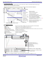
1
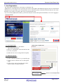
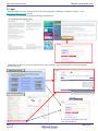
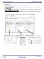
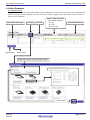
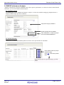
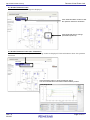
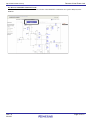
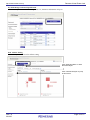
Renesas VP User Manual The Simulation Site for Renesas Power MOSFETs Rev.7.0 2013.07 Overview Renesas VP stands for “Renesas Virtual Power Lab.” and it is the site to simulate the power MOSFET operations of synchronous-rectified buck converters. This site enables to calculate a waveform of buck converters or a loss of power MOSFETs of the power supply in a board around MCUs or SoCs such as POL. Therefore you can select suitable power MOSFETs when you start to design, and also it supports to speed up the evaluation. Before Use The registration to MyRenesas is necessary to use this site. When you register for the first time, please enter your information in the registration page and confirm the checked Renesas VP in the content subscription page. You can access Renesas VP from your profile page of MyRenesas or logos/banners on our website after you have completed the registration. If you are already MyRenesas member, please edit your content subscription and add this service. This site consists of two sections. One is ACTIVE DATASHEET to simulate the characteristic of power MOSFET itself, the other one is BUCK DESIGNER to simulate the operation of buck converters in a model circuit. And the viewer with common functions for a simulated graph allows to scale, move and read the value by its marker. Please refer to the help in a viewer for further information. The target product is mainly the 10th power MOSFETs and later, furthermore, it will be expanded by adding newlydeveloped products. (There are some exceptions.) Precautions • Although the simulation result was confirmed whether it fits an observation result on our test board, it may not get the same results depending on your implementation conditions. Therefore please check the compatibility with customer’s board by adjusting setup conditions or parameters of a model circuit. And this will help to check which parameter works for interested characteristics of customer. • Please use SWITCHING CIRCUIT that simulates only a switching part in view of detailed parameters such as parasitic impedance of boards to check switching a waveform, meanwhile, use SYSTEM SCHEMATIC that simulates the whole circuit, although detailed parameters are omitted, to check loop gains. • The downloadable simulation tool for off-line fulfils its original functions when a downloaded circuit schematic on this site is combined with Renesas power MOSFETs. Please note that it does not fulfill one in case of other combinations by using other manufacturer’s circuit schematics or power MOSFETs. • Please check the latest product status of Power MOSFETs on our website. • If there is no action for over half an hour during simulations, the system makes a time-out error. • The specifications in this system are subject to change without notice. Contact Pease contact Renesas sales offices in your region or use the following contact form. Renesas Electronics Corporation; Customer support contact form http://www.renesas.com/contact/ Rev.7.0 2013.07 Page 1 of 21 Renesas Virtual Power Lab. http://www.renesas.com/vp Index 1. User Registration 1.1. New Registration 1.2. Edit Subscriptions … P. 3 P.3 P.3 2. Login … P.4 3. Landing Page … P.5 4. Active Datasheet 4-1. Product Search 4-2. Product Selection 4-3. Simulation of Each Chart 4-4. Characteristics Map 4-5. Operation of Viewer … P.6 5. Buck Designer (Recommended FETs) 5-1. Condition Setting and Combination Selection 5-2. System Schematic and Switching Circuit 5-3.Wavaform Chart of Each Point 5-4. Efficiency Curve 6. Buck Designer (Custom Solutions) 6-1. Condition Setting 6-2. Custom Combination Setting 7. Buck Designer (Other Functions) 7-1. Design Summary 7-2. Downloadable Simulation Tool 7-3. My Designs 8. DrMOS Performance Analyzer 8-1. Condition Setting 8-2. Product Selection 8-3. DrMOS Solution Circuit 8-4. DrMOS Solution Circuit (after Simulation) 8-5. Discrete MOSFETs Solution Circuit 8-6. Losses & Efficiency 8-7. PCB Design for DrMOS Board Layout 8-8. PCB Design for Discrete Solution Board Layout 8-9. PCB Design for Board Specification 8-10. Airflow Setting 8-11. Thermal Analysis Results 8-12. DrMOS Design Summary Rev.7.0 2013.07 P.6 P.7 P.7 P.8 P.8 … P.9 P.9 P.9 P.10 P.10 … P11 P.11 P.11 … P.12 P.12 P.13 P.13 … P.14 P.14 P.14 P.15 P.15 P.16 P.17 P.18 P.18 P.19 P.19 P.20 P.21 Page 2 of 21 Renesas Virtual Power Lab. http://www.renesas.com/vp 1. User Registration The registration to MyRenesas is necessary to use Renesas VP. MyRenesas is a subscription service provides convenient e-mail updates and additional supports such as tool download. And Renesas VP is provided as one of its premium services. Therefore please confirm the checked “Renesas VP” in the premium service when you register and set up your subscription alerts. If you are already MyRenesas member, you need to edit your content subscription and add this service after logging in. Renesas website 1.1. New Registration (1) Enter you name and e-mail address. (Provisional registration) (2) Receive confirmation e-mail and click the link. (3) Create your profile. (4) Subscribe to services. (Registration complete) 1.2. Edit Subscriptions (1) Login to MyRenesas (2) Click “Edit Subscriptions” in your profile page. (3) Add a check to “Renesas VP” in subscription page. (4) Click “Next”, and your profile page will be appeared again. (Change complete) Profile page of MyRenesas Edit Content Subscription Button to access MyRenesas Rev.7.0 2013.07 Page 3 of 21 http://www.renesas.com/vp Renesas Virtual Power Lab. 2. Login Click the banners or logos of Renesas VP on the power MOSFET related pages of Renesas website or visit http://www.renesas.com/vp directly. Of course, you can access from the profile page of MyRenesas. Ex. Power Devices category page Additionally, it allows to access directly particular Active Datasheet pages from parametric search and product specification pages. Parametric search Particular Active Datasheet Product Specification If your login authentication cash is left, login page is displayed. Rev.7.0 2013.07 Page 4 of 21 Renesas Virtual Power Lab. http://www.renesas.com/vp 3. Landing Page This is the first page of Renesas VP. Two menus and outlines are described. ACTIVE DATASHEET : Enable to grasp the further characteristics with adjusting each parameter compared to a static datasheet. BUCK DESIGNER : Enable to simulate the operation of power MOSFET of synchronous rectification method buck converters. DrMOS PERFORMANCE ANALYZER : Enable to simulate the operation of DrMOS which offers superior performance over discrete solution. ■DrMOS Performance Analyzer Rev.7.0 2013.07 ■BUCK DESIGNER ■ACTIVE DATASHEET Page 5 of 21 Renesas Virtual Power Lab. http://www.renesas.com/vp 4. Active Datasheet 4-1. Product Search The product selection filter and product lineup of power MOSFET is appeared. At first, input search conditions: Part Number, Package, Channel, Rds(on), and Vdss. After that, clicking “Apply” button, the product lineup is narrowed down by your conditions. Part Number (Key input) “Apply” button Package Channel Rds(on) (Slider selection) Vgs condition selection: Any 4.5V 8V or 10V Vdss (Slider selection) “Reset” button Select the check box and click “Apply” button, Package dimensional drawing “Apply” button Rev.7.0 2013.07 Page 6 of 21 Renesas Virtual Power Lab. http://www.renesas.com/vp 4-2. Product Selection Select the product you would like to simulate on this page by reference to parameters or static datasheets. Select button Link to the static datasheet 4-3. Simulation of Each Chart The analysis page of default values is appeared. If you want to continue the simulation by default values, the simulation of all charts starts by clicking “RUN ALL TEST”. If you would like to change the values, please change it by overwriting on the setting page which is appeared by clicking “EDIT” button under each setting table. And start a simulation by clicking “RUN TEST” after that. Download spice data. Simulate all charts. Simulate each chart. Overwrite the value in the BOX. Rev.7.0 2013.07 Page 7 of 21 http://www.renesas.com/vp Renesas Virtual Power Lab. 4-4. Characteristics Map Thumbnails of each chart are appeared after you click “RUN ALL TEST”. The detailed characteristics map is opened in a viewer by clicking these thumbnails. The page of blue-colored text is displayed. : Display all charts : Output characteristic (typ.) : Transfer characteristic : VGS characteristic of VDSON : Drain current characteristic of RDSON : Temp. characteristic of RDSON : VDS characteristic of capacitance : Capacitance change by VGS (Coss, Ciss, Crss) : Reverse current characteristic by VSD : RDSON characteristic by VGS : Switching characteristic Click a thumbnail, and open a viewer. 4-5. Operation of Viewer [Drag] [Zoom In] [Zoom Out] : Move the waveform according to the mouse movement in zoomed mode.. : Enlarges the waveform displayed stepwise by x%. : Shrinks the waveform displayed stepwise by x%. [Marquee Zoom] : Enlarges the waveform in the selected area to the full size of the screen (area zoom). : Go back one zoomed level. [Go back one zoom level] [Go forward one zoom level] : Go forward one zoomed level. : Reset the zoomed mode to its default. [Reset Zoom] : Print the waveforms. [Print Waveforms] Move the position of [M1] and [M2] with dragging vertical lines. Move a selected waveform up. (*) Move a selected waveform down. (*) Select all waveforms. Deselect all waveforms. *; Click an item name to select. Display the values of [M1] and [M2]. Use functions such as RSM, average and peak values. Checking or un-checking the checkbox in front of the waveform name will turn the display on or off. Rev.7.0 2013.07 Page 8 of 21 Renesas Virtual Power Lab. http://www.renesas.com/vp 5. Buck Designer (Recommended FETs) 5-1. Condition Setting and Combination Selection The “Requirements” screen to set conditions is appeared. Set the values of DC/DC converter such as input voltage, output voltage and phases at first. After that, recommended combinations of power MOSFETs which are selected based on your requirements are displayed by clicking “Next” button. Then select the combination you would like to check by clicking “Select” button. Change the values Select the combination • • Click “ ” button to sort the product list. Hover the mouse cursor over “ ” to show explanation of each item. 5-2. System Schematic and Switching Circuit The system schematic is appeared by selecting one of recommended combinations at first. It allows to edit values in the dialogue box by clicking blue-colored one. Note; System circuit and switching circuit are prepared in this converter design page, and blue-colored parameters of both circuits are editable. However, please check the switching circuit to get accurate characteristics because system circuit is omitted some parameters such as floating impedances to keep the calculation scale within its reasonable values. System schematic Switching circuit Efficiency calculation Download schematic Dialogue box to change parameters Rev.7.0 2013.07 Page 9 of 21 http://www.renesas.com/vp Renesas Virtual Power Lab. 5-3. Waveform Chart of Each Point Buttons to show each waveform are appeared in a result space by clicking “Start Simulations” button. Every waveform allows to scale, move and read the value in an original viewer. Gate drive waveform Voltage waveform of control IC Current waveform of inductance Input waveform Output waveform “StartSimulation” button Switching waveform 5-4. Efficiency Curve The efficiency curve of switching circuit is appeared by clicking the tab of “EFFICIENCY CALUCULATION”. This simulation is calculated at the value on set Tch. Therefore when you can not ignore a rise in temperature by the loss, you need to simulate again with adding a resultant rise by multiplying the thermal resistance to a resultant loss of power MOSFET to the initial set values. Excel Data Click “Download” button to download the numerical data in Excel format. Rev.7.0 2013.07 Page 10 of 21 Renesas Virtual Power Lab. http://www.renesas.com/vp 6. Buck Designer (Custom Solutions) 6-1. Condition Setting The “Requirements” screen to set conditions is appeared. Set the values of DC/DC converter such as input voltage, output voltage and phases at first. After that, recommended combinations are displayed by clicking “Next” button. However if you want to try custom solutions, click the tub of “CUSTOM SOLUTIONS” at this time. Edit the values. Click “CUSTOM SOLUTIONS” 6-2. Custom Combination Setting Set a combination you would like to simulate as below, and start a simulation as in case of recommend combinations. (1) Select both high-side FET and low-side FET and set each parallel numeric values. (2) Set combinations are listed here. (3) Display an estimate of loss by clicking “Calculate” button. (4) Start a simulation by clicking “Analyze” button of a good combination after testing some patterns. Rev.7.0 2013.07 Page 11 of 21 http://www.renesas.com/vp Renesas Virtual Power Lab. 7. Buck Designer (Other Functions) 7-1. Design Summary View the summary of a simulation by Buck Designer. Furthermore, you can download the page by PDF format and BOM by Excel format. PDF file ~~~~~~~~~~~~~~~~~~~~~~~~~ BOM ~~~~~~~~~~~~~~~~~~~~~~~~~ Rev.7.0 2013.07 Page 12 of 21 Renesas Virtual Power Lab. http://www.renesas.com/vp 7-2. Downloadable Simulation Tool The simulation tool for off-line is available after a simulation. Fig.1 (1) Download a simulation tool, the data of a system schematic and a switching schematic from the bottom of Design Summary page (Fig.1), and save them to your own PC. Please note that the file may be a large size. Fig.2 Fig.3 (2) Double-click on the simulation tool (Fig2. RenesasVP.exe) to install. The menu of “Renesas-VP” is added to a start menu of your PC (Fig.3) when the installs are done. Fig.4 (3) Click the menu, and click “OK” on the screen (Fig.4) to start. Fig.5 (4) Start a simulation by selecting downloaded data such as a circuit data and a spice data online on the next screen (Fig.5). (5) Although there are some limitations in function, this tool allows to simulation on the screen (Fig.6) by making other circuit data. Note; This tool fulfills its original function when a downloaded circuit schematic on this site is combined with Renesas power MOSFETs. Fig.6 7-3. My Designs Save or load to use again the personal designed data by Buck Designer. Enter a design name Note a additional explanations or comments Saved designs are listed here. Rev.7.0 2013.07 Page 13 of 21 http://www.renesas.com/vp Renesas Virtual Power Lab. 8. DrMOS Performance Analyzer Enable to simulate the operation of DrMOS which offers superior performance over discrete solution. Beside SPICE simulation, you can also simulate thermal analysis. 8-1. Condition Setteing On landing page, select “DrMOS Performance Analyzer”, at first the condition setting page (Requirements) is displayed. Please input operation conditions. Input power supply conditions. Decide package size of DrMOS. Click “Find Parts >>” button to jump to the recommended DrMOS list. 8-2. Product Selection Display the recommended DrMOS product list. Please select part number for simulation. Click “Select” button to jump to simulation page. Click “ ” to show the product feature. Rev.7.0 2013.07 Page 14 of 21 Renesas Virtual Power Lab. http://www.renesas.com/vp 8-3. DrMOS Solution Circuit The selected DrMOS circuit diagram is displayed. Click “Start Simulation” button to start the operation waveform simulation. Click peripheral parts to change parameters (blue text). 8-4. DrMOS Solution Circuit (after Simulation) After simulation, “Input”, “Output”, and “Switching” button are displayed. Click each button to show the operation waveform. Click “Switching” button to show the diagram below. You can zoom waveform and read numerical data by marker. Rev.7.0 2013.07 Page 15 of 21 http://www.renesas.com/vp Renesas Virtual Power Lab. 8-5. Discrete MOSFETs Solution Circuit You can also simulate the discrete MOSFETs solution. This MOSFET combination are equal in Rds(on) to the DrMOS. Rev.7.0 2013.07 Page 16 of 21 http://www.renesas.com/vp Renesas Virtual Power Lab. 8-6. Losses & Efficiency You can compare the losses and efficiency of DrMOS solution with discrete solution. The red line represents DrMOS and the blue line represents discrete. DrMOS has advantage over discrete. The DrMOS and discrete losses are broken down into components. These numerical data are the components of losses. Rev.7.0 2013.07 Page 17 of 21 http://www.renesas.com/vp Renesas Virtual Power Lab. 8-7. PCB Design for DrMOS Board Layout In 8-7. to 8-11. sections, the operation of thermal analysis is explained. This section is about DrMOS board layout design. The heat values of each parts are calculated in aforementioned circuit simulation, and these valued are automatically inputted. Click “Thermal Analysis” to jump to thermal analysis. You can move components by drag-and-drop. 8-8. PCB Design for Discrete Solution Board Lyout Below is a operation screen of discrete solution board layout. Click “Discrete Board Layout” to jump to this screen. Rev.7.0 2013.07 Page 18 of 21 Renesas Virtual Power Lab. http://www.renesas.com/vp 8-9. PCB Design for Board Specification Below is a operation screen for setting board size, thickness and number of layers. 8-10. Airflow Setting below is a operation screen for airflow setting. Click “Start Simulation” to start thermal analysis. Click “Thermal Analysis” to jump to this screen. Rev.7.0 2013.07 Page 19 of 21 Renesas Virtual Power Lab. http://www.renesas.com/vp 8-11. Thermal Analysis Results You can compare the thermal distribution of DrMOS solution with discrete solution. For thermal distribution on board, you can change point of sight: top side, bottom side, front side and back side. Display the temperatures of each components. Rev.7.0 2013.07 Page 20 of 21 Renesas Virtual Power Lab. http://www.renesas.com/vp 8-12. DrMOS Design Summary View the summary of a simulation by “DrMOS Performance Analyzer”. As well as “Back Designer”, you can download the page by PDF format and BOM by Excel format. PDF file download You can save your circuit conditions. Rev.7.0 2013.07 Page 21 of 21