1
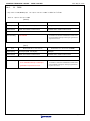
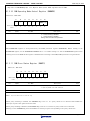
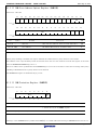
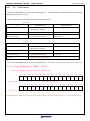
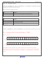
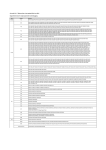
Date: May. 22, 2015 RENESAS TECHNICAL UPDATE 1753, Shimonumabe, Nakahara-ku, Kawasaki-shi, Kanagawa 211-8668 Japan Renesas Electronics Corporation Product Category Document No. MPU/MCU Adds function of “RX64M Group、RX71M Group User’s Manual:Hardware” Title Informatio n Category Lot No. Applicabl e Product RX64M Group RX71M Group RX64M Group: limited RX71M Group:All Reference Document This document describes additions of function in “RX64M Group、RX71M No Chapter No Title Item 1 61 RAM Adds error checking of RAM*1 2 63 Flash memory Adds Unique ID Registers 3 59 Temperature Sensor Adds Temperature Sensor Calibration Data Registers 4 1 Overview Adds Unique ID and error checking of RAM TN-RX*-A127A/E Rev. 1.00 Technical Notification RX64M Group User’s Manual Hardware Rev 1.00 (R01UH0377EJ0100) RX71M Group User’s Manual Hardware Rev 1.00 (R01UH0493EJ0100) Group User's Manual:Hardware” Applicable Product Lot RX64M Group All RX64M Group *2 RX71M Group All RX64M Group *2 RX71M Group All RX64M Group *2 RX71M Group All *1 This item has already described in RX71M Group User's Manual:Hardware. *2 There is the samples which doesn’t apply Unique ID register and Temperature Sensor Calibration Data Registers to RX64M group. This table and figure describes to distinguish the sample which don't have those function. Part No. Package EIA Code The manufacturing lot number R5F564MxxxFC 176pin LQFP(PLQP0176KB-A) 1447、1503 - R5F564MxxxFP 100pin LQFP(PLQP0100KB-A) - 503AZ00 R5F564MxxxFC RX64M TL8400 7 R5F564MxxxFP RX64M 503AZ00 1447 or1503 The manufacturing EIA Code lot number Fig.1 A mark example of LQFP package 176pin (c) 2015. Renesas Electronics Corporation. All rights reserved. FIg.2 A mark example of LQFP package 100pin Page 1 of 10 RENESAS TECHNICAL UPDATE TN-RX*-A127A/E No1. 61 Date: May 22, 2015 RAM ・Page 2716 of 2955(RX64M group) The specifications of RAM is added as follows. Table 61.1 Specifications of RAM 【before】 Item Without ECC Error Correction With ECC Error Correction (ECCRAM) RAM capacity 512 Kbytes (RAM: 512 Kbytes) 32 Kbytes RAM address RAM0: 0000 0000h to 0007 FFFFh ECCRAM: 00FF 8000h to 00FF FFFFh Error checking Not available ・Correction of 1-bit errors and detection of 2-bit errors ・A non-maskable interrupt or interrupt is generated in response to an error. 【after】 Item Without ECC Error Correction With ECC Error Correction (ECCRAM) RAM capacity 512 Kbytes (RAM: 512 Kbytes) 32 Kbytes RAM address RAM0: 0000 0000h to 0007 FFFFh ECCRAM: 00FF 8000h to 00FF FFFFh Error checking ・Detection of 1-bit errors ・A non-maskable interrupt or interrupt is generated in response to an error. ・ECC Error Correction Correction of 1-bit errors and detection of 2-bit errors ・A non-maskable interrupt or interrupt is generated in response to an error. Page 2 of 10 RENESAS TECHNICAL UPDATE TN-RX*-A127A/E 61.2 Register Descriptions adds registers as follows. ・Page 2717 of 2903(RX64M group) 61.2.10 Date: May 22, 2015 RAM Operating Mode Control Register (RAMMODE) Address(es): 0008 1200h b7 b6 b5 b4 b3 b2 - - - - - - 0 0 0 0 0 0 Value after reset: Bit Symbol b1 b0 RAMMODE[1:0] 0 0 Bit Name Description R/W b1, b0 RAMMODE[1:0] RAM Operating Mode Select b1 b0 R/W b7 to b2 - These bits are read as 0. The write value should be 0. R/W Reserved 0 0: Parity checking is disabled. 0 1: Parity checking is enabled. Settings other than above are prohibited. The RAMMODE register is write-protected by the RAM protection register (RAMPRCR). Before writing to the RAMMODE register, set the RAMPRCR.RAMPRCR bit to 1 to enable writing to it. Set the RAMMODE register before starting access to the RAM. If this register is modified after accessing to the RAM, RAM operation is not guaranteed. 61.2.11 RAM Error Status Register (RAMSTS) Address(es): 0008 1201h b7 b6 b5 b4 b3 b2 b1 b0 - - - - - - - RAMERR 0 0 0 0 0 0 0 0 Value after reset: Bit Symbol Bit Name Description b0 RAMERR RAM Error Status Flag 0: A parity check error has not occurred. 1: A parity check error has occurred. b7 to b1 - Reserved These bits are read as 0. The write value should be 0. R/W R/(W)*1 R/W Note 1. Only 0 can be written to clear the flag. When parity checking is enabled, the RAMERR flag is set to 1 if a parity check error is detected. The RAM error interrupt request is also generated at this time. When parity checking is disabled, the RAMERR flag is not set to 1 because no parity check error is detected. Writing 0 to the RAMERR flag clears the RAM error interrupt request corresponding to the parity check error. Page 3 of 10 RENESAS TECHNICAL UPDATE TN-RX*-A127A/E 61.2.12 Date: May 22, 2015 RAM Error Address Capture Register (RAMECAD) Address(es): 0008 1208h Value after reset: b31 b30 b29 b28 b27 b26 b25 b24 b23 b22 b21 b20 b19 - - - - - - - - - - - - - 0 0 0 0 0 0 0 0 0 0 0 0 0 0 0 0 b15 b14 b13 b12 b11 b10 b9 b8 b7 b6 b5 b4 b3 b2 b1 b0 - - - 0 0 0 READ Value after reset: 0 Bit 0 0 0 0 0 0 Bit Name 0 0 0 0 0 b17 b16 READ Description R/W Reserved These bits are read as 0. The write value should be 0. R/W b18 to b3 READ Error Address The address where an error is found is read. b31 to b19 - Reserved These bits are read as 0. The write value should be 0. b2 to b0 Symbol 0 b18 - R R/W When parity checking is enabled, this register will hold the address where a parity check error was found. The address of the 8-byte boundary below the location where the error was found is stored in this register at the same time the RAMSTS.RAMERR flag is set to 1. The error address is not updated when the RAMERR flag is 1 (error has occurred). Its value does not change when parity checking is disabled because no parity check error is detected. The RAMECAD register is initialized only by a reset. 61.2.13 RAM Protection Register (RAMPRCR) Address(es): 0008 1204h b7 b6 b5 b4 b3 b2 b1 RAMPRC R KW[6:0] Value after reset: Bit 0 Symbol 0 0 0 b0 0 Bit Name 0 0 0 Description R/W b0 RAMPRCR RAMMODE Register Write Control 0: Disables writing to the RAMMODE register. 1: Enables writing to the RAMMODE register. R/W b7 to b1 KW[6:0] Write Key Word R/W These bits are read as 0. The write value should be 0. Writing 1 to the RAMPRCR bit is possible when KW[6:0] = 1111000b. Otherwise writing to RAMPRCR clears the bit to 0. Page 4 of 10 RENESAS TECHNICAL UPDATE TN-RX*-A127A/E Date: May 22, 2015 The value of KW[6:0] is read as 0000000b. The targets for write protection by the RAMPRCR register is the RAM operating mode control register (RAMMODE). Once the RAMPRCR bit is set to 1, writing to RAMMODE register is enabled until the RAMPRCR bit is cleared to 0. Clear the RAMPRCR bit to 0 after writing to RAMMODE register. ・Page 2722 of 2903(RX64M group) 61.3 Operation adds 61.3.3 Parity Checking as follows. 61.3.3 Parity Checking Enabling and disabling of parity checking can be selected through the RAMMODE register setting. In the initial state, parity checking is disabled. Even parity checking is used in this device. 1-bit parity check code is added to each 1-byte data for writing, and the parity is checked for reading. If a 1-bit error is detected in the 1 byte when the parity is checked for reading, a RAM error interrupt can be generated. If a 2-bit error or more is detected in the 1 byte, errors cannot be correctly detected. After power-on, parity check code is undefined until data is written. To use parity checking, write the initial value to all areas while parity checking is enabled before accessing to the RAM immediately after a reset. ・Page 2724 of 2903(RX64M group) 61.4 Usage Notes is added as follows. 61.4 Usage Notes 61.4.1 Low Power Consumption Function Power consumption can be reduced by setting module stop control register C (MSTPCRC) to stop supply of the clock signal to the RAM and ECCRAM. Setting the MSTPCRC.MSTPC0 bit to 1 stops supply of the clock signal to the RAM. Setting the MSTPCRC.MSTPC6 bit to 1 stops supply of the clock signal to the ECCRAM. Stopping supply of the clock signal places the RAM and ECCRAM individually in the module stop state. After a reset, the RAM and ECCRAM continue to operate. The RAM and ECCRAM are not accessible in the module stop state. Do not allow transitions to the module stop state while accessing to the RAM or ECCRAM. For details on the MSTPCRC register, refer to section 11, Low Power Consumption. 61.4.2 Notes on Using Error Checking of RAM0 and ECCRAM When using RAM0 parity and ECCRAM ECCs for error checking to operate a program in the relevant RAM, initialize RAM0 and ECCRAM so that CPU can correctly prefetch data. If the CPU prefetches from a RAM area that is not initialized, a RAM error may occur. The RAM0 and ECCRAM should be initialized at the 8-byte boundary. When the end address allocated in the RAM is below the 8-byte boundary, allocate a NOP instruction up to the boundary. Page 5 of 10 RENESAS TECHNICAL UPDATE TN-RX*-A127A/E No2. 63. Date: May 22, 2015 Flash memory ・Page 2726 of 2903(RX64M group)、Page 2746 of 2923(RX71M group) The specifications of Code Flash Memory and Data Flash Memory adds unique ID as follows. Table 63.1 Specifications of Code Flash Memory and Data Flash Memory 【before】 Item Code Flash Memory Memory capacity Data Flash Memory Data area:64 Kbytes User area:4 Mbytes max. User Boot area:32 Kbytes Off-board programming (for products with 100 or more pins) A flash programmer can be used to program the user area and user boot area. A flash programmer cannot be used to program area. 【after】 Item Code Flash Memory Memory capacity Data Flash Memory Data area:64 Kbytes User area:4 Mbytes max. User Boot area:32 Kbytes Off-board programming (for products with 100 or more pins) A flash programmer can be used to program the user area and user boot area. Unique ID A 12-byte ID code provied for each MCU ・Page 2729 of 2903(RX64M group)、Page 2751 of 2923(RX71M group) 63.3.2 63.3 A flash programmer cannot be used to program area. Register Descriptions adds register as follows. Unique ID Register n(UIDRn)(n=0~2) Address(es) UIDR0 007F B174h、UIDR1 007F B1E4h、UIDR2 007F B1E8h b31 b30 b29 b28 b27 b26 Value after reset b24 b23 b22 b21 b20 b19 b18 b17 b16 b5 b4 b3 b2 b1 b0 Unique value for each chip b15 Value after reset b25 b14 b13 b12 b11 b10 b9 b8 b7 b6 チUnique value for each chip The UIDRn registers hold 12-byte ID codes (unique IDs) to identify each MCU. These registers is a 32-bit read-only register. Page 6 of 10 RENESAS TECHNICAL UPDATE TN-RX*-A127A/E No.3 Date: May 22, 2015 59. Temperature Sensor The specifications of Temperature Sensor adds ・Page 2704 of 2903(RX64M group)、Page 2721 of 2923(RX71M group) Temperature sensor calibration data registers as follows. Table 59.1 Specifications of Temperature Sensor 【before】 Item Description Temperature sensor voltage output Temperature sensor outputs a voltage to the 12-bit A/D converter (unit 1). Low-power consumption function The module-stop state is selectable 【after】 Item Description Temperature sensor voltage output Temperature sensor outputs a voltage to the 12-bit A/D converter (unit 1). Low-power consumption function The module-stop state is selectable Temperature sensor calibration data registers Hold the temperature sensor calibration data measured for each chip at the time of shipment. ・Page 2705 of 2903(RX64M group)、Page 2722 of 2923(RX71M group) 59.2.2 59.2 Register Discription add register as follows. Temperature Sensor Calibration Data Register(TSCDR) Address(es) 007F B17Ch Value after reset Value after reset b31 b30 b29 b28 b27 b26 b25 b24 b23 b22 b21 b20 b19 b18 b17 b16 — — — — — — — — — — — — — — — — 0 0 0 0 0 0 0 0 0 0 0 0 0 0 0 0 b15 b14 b13 b12 b11 b10 b9 b8 b7 b6 b5 b4 b3 b2 b1 b0 b31 — b30 — b29 — b28 — b27 b26 b25 b24 b23 b22 b21 b20 b19 b18 b17 b16 0 0 0 0 Unique value for each chip The TSCDR register hold the temperature sensor calibration data measured for each chip at the time of shipment. The temperature sensor calibration data is a digital value converted by the 12-bit A/D converter from the voltage output by the temperature sensor at Ta = Tj = 128ºC and AVCC0 = VREFH0 = 3.3 V. The TSCDR register is a 32-bit read-only register Page 7 of 10 RENESAS TECHNICAL UPDATE TN-RX*-A127A/E ・Page 2705 of 2903(RX64M group)、Page 2722 of 2923(RX71M group) Date: May 22, 2015 59.3.1 Preparation for Using the Temperature Sensor adds a document(the red character) as follows. 59.3.1 Preparation for Using the Temperature Sensor The temperature characteristics of the temperature sensor are shown below. The voltage output by the temperature sensor is proportional to temperature, which can be calculated according to the following formula. Formula for the temperature characteristic: T = (Vs – V1)/Slope + T1 T: Measured temperature (ºC) Vs: Voltage output by the temperature sensor at the time of temperature measurement (V) T1: Temperature experimentally measured at one point (ºC) V1: Voltage output by the temperature sensor at the time of measurement of T1 (V) T2: Temperature at the experimental measurement of another point (ºC) V2: Voltage output by the temperature sensor at the time of measurement of T2 (V) “Slope” indicates the temperature gradient by the temperature sensor (V/ºC); slope = (V2 – V1)/(T2 – T1) Characteristics vary from sensor to sensor. Therefore, the following experimental measurement at two different temperatures is recommended. Use the 12-bit A/D converter to measure the voltage V1 output by the temperature sensor at temperature T1. Again, using the 12-bit A/D converter, measure the voltage V2 output by the temperature sensor at a different temperature T2. Obtain the temperature gradient (slope = (V2 – V1)/(T2 – T1)) from these results. Subsequently, obtain the measured temperature by substituting the slope into the formula for the measured temperature (T = (Vs – V1)/slope + T1). If you are using the temperature gradient given in Table 64.49 of section 64, Electrical Characteristics, the measured temperature can be calculated by using the formula below after simply using the 12-bit A/D converter to experimentally measure the voltage V1 output by the temperature sensor at temperature T1. However, this method gives less accurate temperatures than measurement at two points. T = (Vs – V1)/Slope + T1 T: Measured temperature (ºC) Vs: Voltage output by the temperature sensor at the time of temperature measurement (V) T1: Temperature experimentally measured at one point (ºC) V1: Voltage output by the temperature sensor at the time of measurement of T1 (V) “Slope” indicates the temperature gradient/1000 (V/ºC) given in Table 64.49. The TSCDR registers hold the measured temperature (CAL128) at Ta = Tj =128ºC and AVCC0 = VREFH0 = 3.3 V. Pre-use preparation to obtain this value can be skipped by using the value in the registers as the result of experimental measurement at that point. Page 8 of 10 RENESAS TECHNICAL UPDATE TN-RX*-A127A/E Date: May 22, 2015 This measured value CAL128 can be calculated as follows. V1 = 3.3 × CAL128 / 4096 (V), and this voltage can be used to calculate the measured temperature by using the following formula: T = (Vs – V1) / Slope + 128 (ºC). T: Measured temperature (ºC) Vs: Voltage being output by the temperature sensor at the time of temperature measurement (V) V1: Voltage being output by the temperature sensor at Ta = Tj = 128ºC and AVCC0 = VREFH0 = 3.3 V “Slope” indicates the temperature gradient/1000 (V/ºC) given in Table 64.49. The error characteristic (for a variation of 3σ ) for measured temperatures in the products is as shown in Figure 59.2. Figure 59.2 Error characteristic for Measured Temperatures in Products (from Design Data) RX64M Figure 59.2 Error characteristic for Measured Temperatures in Products (from Design Data) RX71M Page 9 of 10 RENESAS TECHNICAL UPDATE TN-RX*-A127A/E No4. Date: May 22, 2015 1. Overview ・Page 70 of 2903(RX64M group) The outline of Specifications adds as follows. Table 1.1 Outline of Specifications (RX64M) 【before】 Classification Memory Module/Function Description RAM ・Capacity:512 Kbytes ・120MHz、no-wait access 【after】 Classification Memory Module/Function Description RAM ・Capacity:512 Kbytes ・120MHz、no-wait access ・SED (single error detection) Unique ID A 12-byte device-specific ID Page 71 of 2923(RX71M group) The outline of Specifications adds as follows. Table 1.1 Outline of Specifications (RX71M) 【before】 Classification Memory Module/Function Description RAM ・Capacity:512 Kbytes ・0000 0000h to 0003 FFFFh (256 Kbytes): 240 MHz No-wait access 0004 0000h to 0007 FFFFh (256 Kbytes): No-wait access at up to 120 MHz, single wait access at frequencies above 120 MHz. 【after】 Classification Memory Module/Function RAM Description ・Capacity:512 Kbytes ・0000 0000h to 0003 FFFFh (256 Kbytes): 240 MHz No-wait access 0004 0000h to 0007 FFFFh (256 Kbytes): No-wait access at up to 120 MHz, single wait access at frequencies above 120 MHz. ・SED (single error detection) Unique ID A 12-byte device-specific ID Page 10 of 10