1
ACCES I/O PRODUCTS INC
10623 Roselle Street San Diego CA 92121-1506
Tel: (619) 550-9559 FAX: (619) 550-7322
REMOTE ANALOG-to-DIGITAL
CONVERTER
MODEL RAD242
USER MANUAL
File: MRAD242.D2c
Analog-to-Digital Converter Pod
RAD242
User Manual
NOTICES
The information in this document is provided for reference only. ACCES I/O Products Inc does not
assume any liability arising out of the application or use of the information or products described
herein. This document may contain or reference information and products protected by copyrights
or patents and does not convey any license under the patent rights of ACCES, nor the rights of
others.
Printed in USA. Copyright 2002 by ACCES I/O Products Inc, 10623 Roselle Street, San Diego,
CA 92121. All rights reserved.
iii
Analog-to-Digital Converter Pod
RAD242
User Manual
TABLE OF CONTENTS
SOFTWARE . . . . . . . . . . . . . . . . . . . . . . . . . . . . . . . . . . . . . . . . . . . . . . . . . . . . . . . . 1-1
GENERAL . . . . . . . . . . . . . . . . . . . . . . . . . . . . . . . . . . . . . . . . . . . . . . . . . . . . 1-1
COMMAND DESCRIPTIONS . . . . . . . . . . . . . . . . . . . . . . . . . . . . . . . . . . . . . 1-4
DIGITAL INPUT/OUTPUT . . . . . . . . . . . . . . . . . . . . . . . . . . . . . . . . . . . . . . . . 1-4
ERROR CODES . . . . . . . . . . . . . . . . . . . . . . . . . . . . . . . . . . . . . . . . . . . . . . 1-12
INSTALLING THE SOFTWARE . . . . . . . . . . . . . . . . . . . . . . . . . . . . . . . . . . 1-13
RAD242 INITIALIZATION . . . . . . . . . . . . . . . . . . . . . . . . . . . . . . . . . . . . . . . 1-15
HARDWARE . . . . . . . . . . . . . . . . . . . . . . . . . . . . . . . . . . . . . . . . . . . . . . . . . . . . . . . . 2-1
FEATURES . . . . . . . . . . . . . . . . . . . . . . . . . . . . . . . . . . . . . . . . . . . . . . . . . . . 2-1
DESCRIPTION . . . . . . . . . . . . . . . . . . . . . . . . . . . . . . . . . . . . . . . . . . . . . . . . 2-1
BLOCK DIAGRAM . . . . . . . . . . . . . . . . . . . . . . . . . . . . . . . . . . . . . . . . . . . . . . 2-7
INSTALLING THE HARDWARE . . . . . . . . . . . . . . . . . . . . . . . . . . . . . . . . . . . 2-8
SPECIFICATIONS . . . . . . . . . . . . . . . . . . . . . . . . . . . . . . . . . . . . . . . . . . . . . . . . . . . 3-1
INPUT/OUTPUT PIN CONNECTIONS . . . . . . . . . . . . . . . . . . . . . . . . . . . . . . 3-5
WARRANTY . . . . . . . . . . . . . . . . . . . . . . . . . . . . . . . . . . . . . . . . . . . . . . . . . . . . . . . . 4-1
APPLICATION CONSIDERATIONS . . . . . . . . . . . . . . . . . . . . . . . . . . . . . . . . . . . . .
INTRODUCTION . . . . . . . . . . . . . . . . . . . . . . . . . . . . . . . . . . . . . . . . . . . . . .
BALANCED DIFFERENTIAL SIGNALS . . . . . . . . . . . . . . . . . . . . . . . . . . . . .
RS-485 DATA TRANSMISSION . . . . . . . . . . . . . . . . . . . . . . . . . . . . . . . . . .
iv
A-1
A-1
A-1
A-2
Analog-to-Digital Converter Pod
RAD242
User Manual
SOFTWARE
GENERAL
The RAD242 comes with ASCII-based software provided on CD. ASCII programming
permits you to write applications in any high-level language that supports text string
functions, allowing the “REMOTE ACCES” series modules to be used with virtually any
computer that has a RS-485 port.
The communication protocol has two forms: addressed and non-addressed. Nonaddressed protocol is used when only one RAD242 is in use. If more than one RAD242
is in use, or if any other REMOTE ACCES Pod are in use you must use the addressed
protocol. The difference is that an address command is sent to enable the specific pod.
The address command is only sent once during communication between the pod and the
host computer. It enables communication with that specific pod and disables all other
devices on the network.
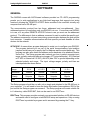
SETUP.EXE: A menu-driven program designed to assist you to configure your RAD242.
The program instructs you on use of the serial communications opto-isolation
jumpers and allows you to specify the Pod Address and the serial baud rate. This
program can also auto-detect the address and/or baud rate of an attached Remote
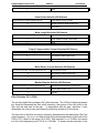
Acces Pod. The Setup program also instructs you how to select converter input
range, polarity mode and bias using jumpers JP7 (unipolar/bipolar), JP6 (External
ref 5 VDC or internal ref 2.5 VDC), and JP5 (bias 2.5V or ground depending on the
selected polarity and range. The input voltage ranges, polarity and bias are
interdependent as shown below.
Range
2.5 V
+/- 2.5 V
5v
+/- 5 v
Reference
Internal
Internal
External
External
Polarity
Unipolar
Bipolar
Unipolar
Bipolar
2.5 V
Ground
2.5 V
Ground
Bias
The Setup program should be run with only a single pod attached to the RS-485 port in
your computer. You will need to know the setup information (base address, IRQ) of the
port so that the Setup program can access it. The Setup program will create a batch file
in it’s directory, called RISC.BAT, that can be used to run RISCTerm.
RISCTerm: This program provides a simple, non-automated interface to RS-485 devices
and can be used to configure or test RAD242 setup and operations. Help on using
RISCTerm is provided in-program and is accessed by pressing the F1 key.
1-1
Analog-to-Digital Converter Pod
RAD242
User Manual
DRIVERS:
COMMDRV.PAS, and COMMDRV.C are communication shortcuts or drivers
provided in C and Pascal source code. Three functions are provided:
“initComCard”, “writePod”, and “readPod”. The functions are polling based with no
IRQ necessary, and deal with strings rather than character-by-character. Consult
the source code files for more information.
SAMPLE:
ACCES provides a sample program that demonstrates reading inputs,
polling the pod for general information, and the use of the driver.
PROGRAM.EXE or WINPROG.EXE: Depending on the exact configuration options
requested when the unit was purchased, you may or may not have this file. This program
is used to upgrade the pod. More information is provided with the program.
Command Structure
All serial communication must be formatted as 7 data bits, even parity, 1 stop bit. All
numbers sent to or received from the pod are in hexadecimal form. The factory default
baud rate is 9600 Baud. The pod is considered to be in addressed mode any time its pod
address is changed from the factory default pod address of 00 (non-addressed mode).
Addressed Mode
The address select command must precede any other command to an addressed pod.
The address command is as follows:
“!xx[CR]”
where xx is the pod address from 01 to FF hex, and [CR] is Carriage
Return, ASCII character 13.
The pod responds with either “xxN[CR]” or “xxY[CR]” if an input change of state has
occurred on enabled bits since the last “Y”or address command. Once the address select
command has been issued, all further commands (other than a new address select) will
be executed by the selected pod. The addressed mode is required when using more than
one pod on the same serial bus.
Non-Addressed Mode
When there’s only one pod connected, no address select command is needed. You can
merely issue commands listed in the following table. Terminology used is as follows:
a. The single lower case letter ‘x’designates any valid hex digit (0-F).
b. The single lower case letter ‘b’designates either a ‘1' or ‘0'.
c. The symbol ‘±’designates either a ‘+’or a ‘-’.
d. All commands are terminated with CR, the ASCII character #13.
e. ALL information is case-sensitive.
f. The symbol ‘*’means zero or more valid characters (total msg length<255
decimal)
1-2
Analog-to-Digital Converter Pod
RAD242
User Manual
General Notes:
ALL numbers passed to and from the Pod are in hexadecimal.
COMMAND LIST
Command
Description
Returns
!xx
Address select command, Selects the pod at address “xx” [CR]
for communication.
CSR=xx
Sets the number of times to read channel 0 before reading
channel 1. If set to 0 it will only read Channel 0
[CR]
CSR?
Returns the current channel ratio loaded in the AD7710
xx[CR]
A0 or A1
Acquires a single channel and returns the data immediately
via the serial port.
=XXXXXX
[CR]
Mxxxx
Configure digital bits as Inputs or Outputs. (1=out,0=in)
[CR]
I
Read all 12 digital inputs.
xxxxxx[CR]
Oxxxx
Writes xxxx to all 12 digital outputs
[CR]
CONTROL?
Returns the control value currently loaded in the AD7710
xxxxxx [CR]
Writes the control value to the AD7710. Please refer to the
control word description below for a definition of possible
values. Used infrequently during initial setup only. Stored
in Flash memory on the AD7710 for future use.
[CR]
CONTROL=xxx
xxx
CSn=xxxxxx
A/D Channel Calibration Scaling Factor
[CR]
Czn=xxxxxx
A/D Channel Calibration Offset Factor
[CR]
CSn?
Czn?
Read Current Scale or Offset Calibration Factor
xxxxxx[CR]
BAUD=xxx
Sets the serial port communications baud rate
=:Baud:0x
V
Queries the firmware Version Number
x.xx[CR]
n
Asks the Pod to resend the previous response
See
description
H*
“Hello” Command. Returns pod name, revision, and
copyright message.
See
description
POD=xx
Sets the pod address to xx
=:Pod#xx
PROGRAM=
Replaces the pod’s EEPROM program, Reserved for factory
use.
[CR]
1-3
Analog-to-Digital Converter Pod
RAD242
User Manual
COMMAND DESCRIPTIONS
The following paragraphs give details of the command functions, describe what the
commands cause and give examples. Please note that all commands have an
acknowledgment response. You must wait for a response from a command before sending
another command.
Address Select
!xx
NOTE
Selects the Pod addressed 'xx'
When using more than one Pod in a system, each Pod is configured with a
unique address. This command must be issued prior to any other
commands to that particular Pod. This command needs to be issued only
once prior to executing anyother commands. Once the address select
command has been issued, that Pod willrespond to all other commands until
a new address select command is issued.
Report Most Recent Analog Data
A0 or A1
Returns the data from the specified channel immediately via the serial
port. The data is normally returned as an equals sign and 6
hexadecimal digits (=xxxxxx). If “16-bit data Word Length”has been
selected with the WL bit in the CONTROL function, the least two
significant digits (8 bits) will always report “FF”.
If the sample returned has already been read, the equals sign will
instead be a slash (/xxxxxx).
The channel specified in the parameter is acquired using the polarity, gain specified and
corner frequency that was configured using the “CONTROL =” command.
Channel Sample Ratio Control
CSR=xx
Sets the channel sample ratio to ‘xx’
CSR?
Read back the channel sample ratio
With the channel sample ratio set to zero, the pod will not read channel 1 at all. With any
other value, the pod will take a number of samples from channel 0 equal to the CSR before
each sample taken from channel 1. Due to the nature of Sigma-Delta A/D convertions, a
number of samples are “thrown away”by the pod each time it changes channels. For this
reason, optimizing channel selection via the CSR command is recommended.
DIGITAL INPUT/OUTPUT
Configure Bits as Input or Output
1-4
Analog-to-Digital Converter Pod
Mxxxx
RAD242
User Manual
Configure digital bits as input or output.
This function programs, on a bit-by-bit basis, the digital bits as input or output. A “zero”
in any bit position of the xxxx control byte designates the corresponding bit as an input.
Conversely, a “one” designates a bit to be configured as an output. (Note: Any bit
configured as an output can still be read as an input if the current value output is a “one”.
Examples:
Program even bits as outputs, and odd bits as inputs.
SEND:
MAAAA
RECEIVE:
[CR]
Program bits 0-7 as input, and bits 8-F as output.
SEND:
MFF00
RECEIVE:
[CR]
Read Digital Inputs
I
Read 12 bits
These commands read the digital input bits from the pod. All byte or word wide responses
are sent most-significant nibble first.
Examples:
Read ALL 12 bits.
SEND:
I
RECEIVE: FFFFFF[CR]
Write Digital Outputs
Oxxxx Write to all 12 digital output bits
This command write outputs to digital bits. Any attempt to write to a bit configured as input
will fail. Writing to a word wherein some bits are input and some are output will cause the
output latches to change to the new value, but the bits which are inputs will not output the
value until/unless they are placed in output mode.
Single bit commands will return an error (4) if an attempt is made to write to a bit
configured as an input.
Writing a “one” to a port asserts the pull-down. Writing a zero de-asserts the pull-down.
Therefore, if the factory installed +5V pull-up is installed, writing a one will cause zero volts
to be at the connector, and writing a zero will cause +5 volts to be asserted. If the factory
installed pull-up has been removed, the user supplied pull-up will be asserted.
1-5
Analog-to-Digital Converter Pod
RAD242
User Manual
Examples:
Write zeros to bits 0-7, and ones to 8-11
SEND:
OFF00
RECEIVE:
[CR]
CONTROL REGISTER PROGRAMMING
The A/D chip contains a 24-bit control register accessible using the CONTROL=xxxxxx and
CONTROL? commands. These commands write and read the control register’s value.
The following table shows the bits comprising the control register. Writing the 6-digit hex
number which contains the correct bit pattern for the control function you wish to perform
will set and clear the bits in the A/D chip.
It is important to write at least one CONTROL=xxxxxx value for each channel you are
going to acquire. This will configure the range, corner frequency, and other options for the
channel you specify.
For most applications, set the MD2-0 bits to “000" or, before you start taking data, set the
bits to “001" one time per channel to do a quick self-calibration.
The PD bit should be left “0". Setting this bit to “1" will prevent the pod from acquiring
data, as it forces the A/D into low-power mode.
23
22
21
20
19
18
17
16
15
14
13
12
MD2
MD1
MD0
G2
G1
G0
CH
PD
WL
IO
BO
B/U
FS11
FS10
FS09
FS08
FS07
FS06
FS05
FS04
FS03
FS02
FS01
FS00
11
10
09
08
07
06
05
04
03
02
01
00
MD2-MD0 Operations Mode Bit Selection Options
MD2
MD1
MD0
Operating Mode Description
0
0
0
Normal Mode. This is the normal mode of operation of the device. This
is the default condition of these bits after initial power on reset.
0
0
1
Active Self-Calibration. This activates self-calibration on the channel
selected by CH (Bit 17 of the control register). This is a one-step
calibration sequence, and when complete, the part returns to the normal
mode (MD2-MD0 = 000). For this calibration type, the zero scale
calibration is done internally on shorted (zero) inputs and the full-scale
calibration is done internally on VREF.
1-6
Analog-to-Digital Converter Pod
RAD242
User Manual
0
1
0
Activate System Calibration. This activates system calibration on the
channel selected by CH (Bit 17 of the Control Register). This is a twostep calibration sequence, with the zero scale calibration done first on the
selected input channel. The part returns to normal mode (MD2-MD0 =
000) at the end of this first step in the two-step sequence.
0
1
1
Activate System Calibration. This is the second step of the system
calibration sequence, with the full-scale calibration being performed on
the selected input channel. When this calibration is complete, the part
returns to the normal mode.
1
0
0
Activate System Offset Calibration. This activates system offset
calibration on the channel selected by CH. This is a one-step calibration
sequence and, when complete, the part returns to the normal mode. For
this calibration type, the zero scale calibration is done on the selected
input channel and the full-scale calibration is done internally on VREF.
1
0
1
Active Background Calibration. This activates background calibration on
the channel selected by CH. If the background calibration mode is on,
then the AD7710 provides continuous self-calibration of the reference and
shorted (zeroed) inputs. The calibration takes place as part of the
conversion sequence, extending the conversion time and reducing the
word rate by a factor of six. Its major advantage is that the user does not
have to worry about recalibrating the device when there is a change in the
ambient temperature. In this mode, the shorted (zeroed) inputs and
VREF, as well as the analog input voltage, are continuously monitored
and the calibration registers of the device are automatically updated.
1
1
0
Read/Write Zero Scale Calibration Coefficients. This is accessed using
the Czn=xxxxxx command.
1
1
1
Read/Write Full-Scale Calibration Coefficients. This is accessed using
the Csn=xxxxxx command.
Programmable Gain Amplification Bit Pattern
G2
G1
G0
Gain
0
0
0
1 (Default condition
after internal power-on
reset)
0
0
1
2
0
1
0
4
0
1
1
8
1
0
0
16
1
0
1
32
1
1
0
64
1
1
1
128
Channel Selection Bit Patterns
Channel CH (Control Register Bit 17)
Channel Selected
0
AIN1 (Default condition after POR)
1-7
Analog-to-Digital Converter Pod
RAD242
1
User Manual
AIN2
Power-Down Selection Bit Patterns
Power-Down PD (Control Register Bit 16)
Power Status of AD7710 Chip
0
Normal Operation (Default after POR)
1
Power-Down
Word Length Selection Bit Patterns
Word Length WL (Control Register Bit 15)
Output Word Length
0
16-Bit (Default condition after POR)
1
24-Bit
Output Compensation Current Selection Bit Patterns
Current Output IO (Control Register Bit 14)
Output Compensation Current
0
Off (Default condition after POR)
1
On
Break Detect Current Selection Bit Patterns
Burn-Out Current BO (Control Register Bit 13)
Device Break Current
0
Off (Default Condition After POR)
1
On
Bipolar/Unipolar Selection Bit Patterns
Bipolar/Unipolar B/U (Control Register Bit 12)
Bipolar/Unipolar Selection for both Inputs
0
Bipolar (Default after POR)
1
Unipolar
Filter Selection (FS11-FS00)
3
The on-chip digital filter provides a Sin c filter response. The 12 bits of data programmed
into these bits determine the filter cutoff frequency, the position of the first notch of the
filter and the data rate for the part. In association with the gain selection, it also
determines the output noise (and hence the effective resolution) of the device.
The first notch of the filter occurs at a frequency determined by the relationship: filter first
notch frequency = (fclk IN/512)/CODE Where code is the decimal equivalent of the code in bits
FS00 to FS11 and is in the range 19 to 2000. With nominal fclk IN of 10 MHz, this results
in a first notch frequency from 9.76 Hz to 1.028 Khz. To ensure correct operation of the
1-8
Analog-to-Digital Converter Pod
RAD242
User Manual
AD7710, the value of the code loaded to these bits must be within this range. Failure to
do this will result in unspecified operation of the device.
Changing the filter notch frequency, as well as the selected gain, impacts resolution. The
output data rate (or effective conversion time) for the device is equal to the frequency
selected for the first notch of the filter. For example, if the first notch of the filter is selected
at 50 Hz, then a new word is available at a 50 Hz rate or every 20 mSec. If the first notch
is at 1 Khz, a new word is available every 1 mSec.
The settling time of the filter to full-scale step input change is worst case 4 x 1/(output data
rate). This settling time is to 100% of the final value. For example, with the first notch filter
at 50 Hz, the settling time of the filter to full-scale step input change is 80 mSec maximum.
If the first notch is at 1 Khz, the settling time of the filter to a full-scale input step is 4 msec
maximum. This settling time can be reduced to 3 x 1/(output data rate) by synchronizing
the step input change to a reset of the digital filter. In other words, if the step input time
takes place with SYNC* low, the settling time will be 3 x 1/(output data rate). If a change
of channels takes place, the settling time is 3 x 1/(output data rate) regardless of the
SYNC* input.
The -3 db frequency is determined by the programmed first notch frequency according to
the relationship: filter -3 db frequency = 0.262 x first notch frequency.
Set a New Baud Rate (When shipped by ACCES, the baud rate is set at 9600.)
BAUD=xxx
Program the pod with a new baud rate
This command sets the pod to communicate at a new baud rate. The parameter passed,
xxx, is slightly unusual. Each x is the same digit from the following table:
CODE
BAUD RATE
0
1,200
1
2,400
2
4,800
3
9,600
4
14,400
5
19,200
6
28,800
7
57,600
Therefore, valid values for the command’s “xxx”are 000, 111, 222, 333, 444, 555, 666, or
777.
The pod returns a message indicating it will comply. The message is sent in the old baud
rate, not the new one. Once the message is transmitted, the pod changes to the new baud
rate. The new baud rate is stored in EEPROM and will be used even after power-reset,
until the next “BAUD=xxx” command is issued.
1-9
Analog-to-Digital Converter Pod
RAD242
User Manual
Example:
Set the pod to 19200 baud.
SEND:
RECEIVE:
BAUD=555
=:Baud:05[CR]
Set the pod to 9600 baud.
SEND:
RECEIVE:
BAUD=333
=:Baud:03[CR]
Read Firmware Revision Number
V
Read the firmware revision number
Reads the version of firmware installed in the pod. It returns “X.XX[CR]”.
Example:
Read the RAD242 version number.
SEND:
V
RECEIVE: 1.00[CR]
NOTE:
The “H”command returns the version number along with other information.
Resend Last Response
n
Resend last response
This command will cause the pod to return the same thing it just sent. This command
works for all responses less than 255 characters in length. Normally this command is used
if the host detected a parity or other line fault while receiving data, and needs the data to
be sent a second time.
The “n” command may be repeated.
Example:
Assuming the last command was “I”, ask pod to resend last response.
SEND:
n
RECEIVE:
FFF[CR]
;or whatever the data was
Hello Message
H*
Hello message
Any string of characters starting with “H” will be interpreted as this command. (“H[CR]”
alone is also acceptable.) The return from this command takes the form (without the
quotes):
1-10
Analog-to-Digital Converter Pod
RAD242
User Manual
“=Pod aa, RAD242 Rev rr Firmware Ver:x.xx ACCES I/O Products, Inc.”
aa is the pod address
rr is the hardware revision, such as “B1"
x.xx is the software revision, such as “1.00"
Example:
Read the greeting message.
SEND:
RECEIVE:
Hello?
=Pod 00, RAD242 Rev B1 Firmware Ver:1.00
ACCES I/O Products, Inc.[cr]
Program the Pod Address
POD=xx
Program the currently selected pod to respond at address xx
This command changes the pod’s address to xx. If the new address is 00, the pod will be
placed into non-addressed mode. If the new address is not 00, the pod will not respond
to further communications until a valid address command is issued. Hex numbers 00-FF
are considered valid addresses. The R specification allows only 32 drops on the line, so
some addresses may be unused.
The new pod address is saved in EEPROM and will be used even after power-down until
the next “POD=xx” command is issued. Note that, it the new address is not 00 (i.e., the
pod is configured to be in addressed mode), it is necessary to issue an address command
to the pod at the new address before it will respond.
The pod returns a message containing the pod number as confirmation.
Example:
Set the pod address to 01.
SEND:
RECEIVE:
POD=01
=:Pod#01[CR]
Set the pod address to F3.
SEND:
RECEIVE:
POD=F3
=:Pod#F3[CR]
Take the pod out of addressed mode.
SEND:
RECEIVE:
POD=00
=:Pod#00[CR]
Enter a New Program
PROGRAM= This command initiates transfer of a new program to the RAD242.
1-11
Analog-to-Digital Converter Pod
RAD242
User Manual
This command should be used carefully. If you accidentally issue a “PROGRAM=”
command, ESC (ASCII 27) will restart the pod as if power had been reset. This feature is
designed to allow ACCES to provide field-upgrades to the RAD242 firmware, and, for
advanced users, the opportunity to customize the firmware in the pod. Documentation
relating to use of this command is provided with the upgrade CD, or is available separately
for a small fee.
| (Vertical Bar) =
Same as the PROGRAM command except it is used only after
a reset has occured. Allows access to POD to download new
firmware.
ERROR CODES
The following error codes can be returned from the pod:
1:
3:
4:
9:
Invalid channel number (too large, or not a number. All channel numbers
must be between 00 and 17, in hex. (0-24 decimal)).
Improper Syntax. (Not enough parameters is the usual culprit).
Channel number is invalid for this task (For example if you try to output to
a bit that is set as an input bit, that will cause this error).
Parity error. (This occurs when some part of the received data contains a
parity or framing error).
Additionally, several full-text error codes are returned. All begin with “Error, ” and are
useful when using a terminal to program the pod.
Error, Unrecognized Command: {command received}[CR]
This occurs if the command is not recognized.
Error, Command not fully recognized: {Command received}[CR]
This occurs if the first letter of the command is valid, but the remaining
letters are not.
Error, Address command must be CR terminated[CR]
This occurs if the address command (!xx[CR]) has extra characters between
the pod number and the [CR].
1-12
Analog-to-Digital Converter Pod
RAD242
User Manual
INSTALLING THE SOFTWARE
You have received with your product a CD that contains all the software you need to use
your card. The CD is compatible with any type of Windows or DOS system.
To install the software required for your card:
1.
Insert CD in your CD ROM - If the install program does not start within 30
seconds, run “install.exe” from the root directory of the CD.
2.
Click the Install Software to Hard Disk button.
3.
Select the product you wish to install from the list shown.
4.
Click Next.
5.
The CD creates a directory with a default name; if you want to change it,
click Change and select the path you prefer.
6.
We advise you to also install the Tools Package at least once per system.
7.
Click Quick Install to run the install process or click Detailed Install if you
want more information on the files installed.
8.
Click Finish.
9.
Click Exit install program when finished.
You now have two types of files on your hard disk:
1. Software, including samples in C, Pascal, QuickBasic and a setup program, specifically
for your card.
2. Software to help you use ACCES cards under a variety of environments:
Setup.exe
Setup program
Findbase.exe
DOS utility to determine an available base address for ISA bus , non-PnP
cards. Run this program once, before the hardware is installed in the
computer, to determine an available address to give the card. Once the
address has been determined, run the setup program provided with the
hardware to see instructions on setting the address switch and various
option selections.
Poly.exe
A generic utility to convert a table of data into an nth order polynomial.
Useful for calculating linearization polynomial coefficients for
thermocouples and other non-linear sensors.
Risc.bat
A batch file demonstrating the command line parameters of RISCTerm.exe.
1-13
Analog-to-Digital Converter Pod
RISCTerm.exe
In the ACCES32
directory:
RAD242
User Manual
A dumb-terminal type communication program designed for RS422/485
operation. Used primarily with REMOTE ACCES data acquisition Pods
and our RS422/485 serial communication product line. Can be used to say
hello to an installed modem. RISCTerm stands for Really Incredibly Simple
Communications TERMinal
This directory contains the Windows 95/98/NT driver used to provide
access to the hardware registers when writing 32-bit Windows software.
Several samples are provided in a variety of languages to demonstrate
how to use this driver. The DLL provides four functions (InPortB,
OutPortB, InPort, and OutPort) to access the hardware.
This directory also contains the device driver for NT. This device driver
provides register-level hardware access from Windows NT, normally called
through ACCES32.DLL. Two methods of using the driver are provided, the
ACCES32.DLL (recommended) and the DeviceIOControl handles direct to
the SYS file (slightly faster)
ACCES95 and ACCESNT
These two drivers are mentioned for users migrating from older versions of
ACCES Tools. The functionality of ACCES95 and ACCESNT has been
combined into ACCES32.DLL, which is described up
.
In order to modify your software to use the new ACCES32.DLL, change the
file you link to from ACCES95 or ACCESNT to ACCES32. No other changes
are necessary.
If you want to avoid recompiling software that was written for ACCES95 or
ACCESNT, just rename ACCES32.DLL to the appropriate name (95 or NT).
In the BSAMPLES
directory:
A Quickbasic sample.
In the CSAMPLES
directory:
In the PCI
directory:
In the PSAMPLES
directory:
In the VBACCES
directory:
Samples in C.
This directory contains PCI-bus specific programs and information. If you
are not using an ACCES PCI card, you can ignore or delete this directory.
This directory contains samples in Pascal
Sixteen-bit DLL drivers for use with VisualBASIC 3.0 and Windows 3.1 only.
These drivers provide four functions, similar to the ACCES32 DLL.
However, this DLL is only compatible with 16-bit executables. Migration
from 16-bit to 32-bit is simplified because of the similarity between
VBACCES and ACCES32.
1-14
Analog-to-Digital Converter Pod
In the WIN32IRQ
directory:
RAD242
User Manual
you have utility software to handle IRQs from any card under Win95/98 or
NT
1. Drivers.src with 3 subdirectories
a. DLL
Samples for using ACCES32.DLL are provided in this directory.
Using this DLL not only makes the hardware programming easier
(MUCH easier), but also one source file can be used for both
Windows 95/98 and WindowsNT. One executable can run under
both operating systems and still have full access to the hardware
registers. The DLL is used exactly like any other DLL, so it is
compatible with any language capable of using 32-bit DLLs. Consult
the manuals provided with your language’s compiler for information
on using DLLs in your specific environment.
b. SYS
The samples in this directory are provided ONLY for WindowsNT.
The DeviceIOControl based interaction with the register-level driver
is only available in NT. If your code is written to use this method, it
will not work with Windows 95 or Windows 98.
The SYS file is the actual workhorse behind hardware access in
WindowsNT. It utilizes the DeviceIOControl API function for
interaction with user code. Samples are provided demonstrating this
API call, but it is strongly recommended that the DLL interface be
used. The DLL described above encapsulates the SYS file and
performs the DeviceIOControl calls at a small penalty in speed. (A
call through the DLL interface)
c. VXD
source fo the driver
2. Samples: Samples in VisualC, Delphi and C++ Builder
RAD242 INITIALIZATION
1. Run the setup program from the directory that the software was installed. Use the
menus to set jumper J5 (Vref internal 2.5V or external 5V), jumper J6 (polarity/unipolar or
bipolar) and jumper J7 (bias 2.5V or ground depending on selected range and polarity).
2. Apply power to the card connected to the serial bus.
3. Setup the gain, word length, channel number, range and polarity for the card by
programming the control register bits 20-12. Review the Control Register Programming
Section starting on page 3-9 of this manual. Set the digital notch filter frequency by writing
a bit pattern into bits 11-0 of the control register.
4. The setup program creates a batch file called “RISC.BAT”. Run this program to run
RISCTERM using the “CONTROL=” command in RISCTERM.
1-15
Analog-to-Digital Converter Pod
RAD242
User Manual
5. Perform the calibration routine for Channel 1 (see paraaragraph “Calibration”in Chapter
2 of the manual).
6. Perform the calibration routine for Channel 2.
1-16
Analog-to-Digital Converter Pod
RAD242
User Manual
HARDWARE
FEATURES
!
!
!
!
!
!
!
!
!
!
Remote Intelligent Analog/Digital I/O Unit with Opto-Isolated RS-485 Interface
to Host Computer.
Higher Baud Rates and Simpler Programming Than Competitor Units.
NEMA 4 Enclosure for Harsh Atmospheric and Marine Environments.
Type 8031 Microcontroller with 32K x 8 bits RAM and 8K x 8 bits EEPROM.
(32k x 8 bits optional)
2-Channel 24-Bit Analog/Digital Delta-Sigma Converter.
Bi-polar and Unipolar Voltage Input Ranges of 2.5 V and 5 V.
Self-Calibrating or Auto-Calibrating Modes to Eliminate Drift Errors.
12-Bit Digital Port with Each Bit Programmable as Either Input or Output.
Constant Current Source for Thermocouple Cold-Junction Compensation.
All Programming in Software, few jumpers
DESCRIPTION
Model RAD242 is an intelligent, two-channel, 24-Bit analog-input interface unit. It is
packaged in a NEMA4 enclosure for remote installation in harsh environments.
Communication with the host computer is via EIA RS-485, half-duplex, serial
communications protocol.
ASCII-based command/response protocol
permits
communication with virtually any computer system that has an Asynchronous RS-485 port.
RAD242 is one of a series of remote intelligent pods called the “REMOTE ACCES”Series.
As many as 32 “REMOTE ACCES” Series pods may be connected on a single two-wire
multi-drop RS-485 network. Each unit has a unique address. Communication uses a
master/slave protocol wherein the pod talks only if questioned by the computer.
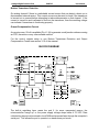
The enclosure contains three boards:
1. The microcontroller board
2. Personality board
3. Termination board
The microcontroller board’s type 8031 microcontroller (with 32x8K RAM, 8x8K non-volatile
EEPROM, and a watchdog timer circuit) gives RAD242 the capability and versatility
expected from a modern distributed control system. To accommodate special programs,
the EEPROM can be expanded to 32x8K. RAD242 contains CMOS low-power circuitry,
an optically-isolated receiver/transmitter, and power conditioners for local and external
isolated power. It can operate at baud rates up to 57.6 Kbaud and distances up to 4000
feet with low-attenuation twisted-pair cabling.
All programming of RAD242 is in ASCII-based software. ASCII-based programming permits
you to write applications in any high-level language that supports ASCII string functions and
you can use ACCES “R” series pods with virtually any computer.
2-1
Analog-to-Digital Converter Pod
RAD242
User Manual
The module, or pod, address is programmable from 00 to FF hex and whatever address is
assigned is stored in EEPROM and used as the default address at the next Power-ON.
Similarly, the baud rate is programmable for 1200, 2400, 4800, 9600, 14400, 19200, 28800,
and 57600. The baud rate is stored in EEPROM and used as default at the next Power-ON.
The personality board has mounted on it the interface connector (J1) and two 20-pin
connectors P2 and J3 for mating to the microcontroller board connectors J2 and P3.
The personality board consists of three sections:
1. Analog section
2. Digital section
3. Power supply section
The layout of each section is discussed below.
Analog Section:
The analog section contains the input filters, the external 5 V reference, the analog-todigital converter and the crystal. There are three jumpers JP5, JP6 and JP7 which are used
to select polarity, range and bias. The analog-to-digital converter has two differential input
channels. Channel 1 is used to measure the input signal while Channel 2 can be
configured to be identical to Channel 1 or configured to measure the +/- 7.5 VDC excitation
voltage Vexc.
Digital Section:
The digital section consists of digital input buffers, digital output latches with their
associated high current open collector sinks, and pull-up resistors.
Power Supply Section:
The power supply section consists of power regulators that supply regulated voltages for
the digital and analog circuits, sensor excitation and an isolated voltage for the RS485
serial communications circuit. The internal voltages are 5 VDC digital supply, +/- 5.5 VDC
analog supplies, +/- 7.5 VDC sensor excitation and +5 VDC isolation power.
Delta-Sigma Converter
Model RAD242 uses a Delta-Sigma analog-to-digital converter with on-chip digital filtering
providing a complete analog front end for low frequency measurement applications. DeltaSigma converters contain a charge balancing ADC, a calibration microcontroller with an onchip static RAM, a clock oscillator and a digital filter.
2-2
Analog-to-Digital Converter Pod
RAD242
User Manual
Basic Theory of Operation
The input signal to the selected analog input channel is continuously sampled at a rate
determined by the frequency of the master clock and the selected gain. A chargebalancing A/D converter (Sigma-Delta Modulator) converts the sampled signal into a digital
pulse train whose duty cycle contains the digital information. The programmable gain
function on the analog input is also incorporated in the modulator, with the input sampling
frequency being changed to provide higher gains. A digital low-pass filter processes the
output of the modulator and updates the output register at a rate that is determined by the
first notch frequency of the low-pass filter. The output data can be read from the serial port
randomly or periodically at any rate up to the output register update rate. The first notch
of this digital filter can be programmed via an on-chip control register. The programmable
range for this first notch frequency is from 9.76 Hz to 1.028 Khz, giving a programmable
range for the -3 db frequency of 2.58 Hz to 269 Hz.
Detailed Theory of Operation
The sigma-delta ADC contains the following elements:
1.
2.
3.
4.
5.
6.
A sample-hold amplifier.
A differential amplifier or subtractor
An analog low-pass filter
A 1-bit A/D converter (comparator)
A 1-bit DAC
A digital low-pass filter
The analog signal sample is fed to the subtractor, along with the output of the 1-bit DAC.
The filtered difference signal is then fed to the comparator, whose output then samples the
difference signal at a frequency many times that of the analog signal sampling frequency.
This is called oversampling. The sigma-delta converter samples the input signal at a
frequency of 19.5 Khz or greater dependent on the required gain to reduce the noise by
spreading the noise energy of each sample over the entire measurement period resulting
in a high-accuracy, low-noise measurement from the 1-bit A/D converter. This architecture
is inherently monotonic (there is an output number for any analog input) and provides very
high accuracy but at the expense of measurement speed (or data output rate). To achieve
22 bits of accuracy at a 10MHz clock frequency resulting in a data or measurement rate of
less than 10Hz.
The output of the comparator provides the digital input for the 1-bit DAC allowing the
system to function as a negative feedback loop that minimizes the difference signal. The
digital data that represents the analog input voltage is contained in the duty cycle of the
pulse train appearing at the output of the comparator and can be retrieved as a parallel
binary data word using a digital filter. The second order sigma-delta modulator and a digital
filter provides a rolling average of the sampled output. After power-up or if there is a step
change in the input voltage, there is a settling time that must elapse before valid data is
obtained. In most signal processing and analysis applications this lag is insignificant.
However, in real-time control applications, this lag should be carefully considered and
analyzed.
2-3
Analog-to-Digital Converter Pod
RAD242
User Manual
Programmable Digital Filter
The internal digital filter removes noise added during the conversion and sums the
oversampled readings to produce multiple bit measurements at a data update rate
determined by the first notch of the digital filter. Internally, the converter provides
measurements at a 19.5 kHz output rate and is filtered down to the update rate defined by
the digital filter. The cutoff frequency of the digital filter is determined by the value loaded
to bits FS0 to FS11 in the control register. At the maximum clock frequency of 10 MHz, the
minimum cutoff frequency of the filter is 2.58 Hz while the maximum programmable cutoff
frequency is 269 Hz. Since the ADC contains the on-chip, low-pass filtering, there is a
settling time associated with step function inputs. Data on the output will be invalid after
a step change until the settling time has elapsed. The settling time depends on the notch
frequency chosen for the filter. The output data rate equates to the filter notch frequency
and the settling time of the filter to a full-scale step input that is four times the output data
period. In applications using both input channels, the settling time of the filter must be
allowed to elapse before data from the second channel is accessed.
Post filtering may be used to increase the update rate or reduce the output noise. For
example, if the bandwidth is 7.86 Hz, but the desired update rate is 100 Hz, the data could
be taken at the 100Hz rate giving a -3 dB bandwidth of 26.2 Hz. Post filtering can be
applied to this to reduce the bandwidth and output noise, to the 7.86 Hz bandwidth level,
while maintaining an output rate of 100 Hz.
Post filtering can also be used to reduce the output noise from the device for bandwidths
below 2.62 Hz. At a gain of 128, the output RMS noise is 420 nV. This is essentially device
noise or white noise, and since the converter uses a chopper-stabilized input stage to
reduce input drift, the noise has a flat frequency response. By reducing the bandwidth
below 2.62 Hz, the noise in the resultant passband can be reduced. A reduction in
bandwidth by a factor of two results in a
reduction in the output rms noise. This
additional filtering will also result in a longer settling time.
The worst-case settling time of the filter to a full-scale step input change is 4x the data rate.
For example, with the first filter notch at 50 Hz, the full-scale step settling time of the filter
would be 80 ms (maximum).
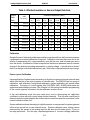
Due to a digital signal processing method used by the sigma-delta converter in the
RAD242, changing the channel gain, in addition to the output sample rate, impacts the
resolution. In the following table the effective resolution is defined as the magnitude of the
output rms noise with respect to the input full scale (i.e.; 2x VREF /Gain) for a VREF of +2.5V.
2-4
Analog-to-Digital Converter Pod
RAD242
User Manual
Table 1: Effective Resolution vs Gain and Output Data Rate
Output
Data
Rate
Effective Resolution (Bits)
- 3dB
Frequency
Gain
of 1
Gain
of 2
Gain
of 4
Gain
of 8
Gain
of 16
Gain
of 32
Gain
of 64
Gain
of 128
10 Hz
2.62 Hz
21.5
21.5
21.5
20.5
19.5
18.5
17.5
16.5
25 Hz
6.55 Hz
20
20
20
20
19.5
18.5
17.5
16.5
30 Hz
7.86 Hz
19.5
20
20
19.5
19.5
18.5
17.5
16.5
50 Hz
13.10 Hz
19.5
19.5
19.5
19.5
19
18.5
17.5
16.5
60 Hz
15.72 Hz
19
19.5
19.5
19.5
19
18.5
17.5
16.5
100 Hz
26.20 Hz
18.5
18.5
18.5
18.5
18
17.5
17
16
250 Hz
65.50 Hz
15
15
15.5
15.5
15.5
15.5
15
14.5
500 Hz
131.00 Hz
13
13
13
13
13
12.5
12.5
12.5
1 kHz
262.00 Hz
10.5
10.5
11
11
11
10.5
10
10
Calibration
Despite the use of inherently stable sigma-delta converters with low-drift and noise immune
components occasional calibration is required. Calibration removes the errors due to the
effects of temperature drift, supply sensitivity, time drift on zero, and full scale gain errors
from the device. A calibration routine is required on the devices whenever there is a known
change in the ambient operating temperature or supply voltage. It should also be done if
there is a change in the selected channel, gain, filter notch or bipolar/unipolar input range.
Power up and Calibration
Upon application of system power the analog-to-digital converter performs an internal reset
which sets the bits in the control register to a known state. The RAD242 has four types of
calibration, self-calibration, background calibration, system calibration and system offset
calibration. The setup of control register bits 23-21(MD2, MD1 & MD0) determines the
operational and calibration modes. (See Chapter 3 of this manual for detailed programming
of the control register) Information on the calibration modes follows.
In the self-calibration mode the zero scale point used in determining the calibration
coefficient is done with both inputs being shorted internally. The full-scale coefficient is
determined by the span between the shorted inputs conversion and the conversion on the
internal reference node Vref.
System calibration allows the analog-to-digital converter to compensate for system gain and
offset errors as well as its own internal errors. System calibration uses voltage values
presented by the system to the analog input for the zero and full-scale points. This is a
two-step procedure. The first step requires application of the zero voltage (calibration
2-5
Analog-to-Digital Converter Pod
RAD242
User Manual
register bits MD2, MD1 & MDO will have a 0, 1, 0 written to them). In the second step the
full scale point is applied to both inputs. The second step is then initiated by writing a 0,
1, 1 to control register bits MD2, MD1 & MD0 respectively. The applied input voltages must
be stable during each step of the calibration procedure.
In the system offset calibration the zero scale point is determined by the conversion of the
zero voltage presented to the input of the converter analog input. The full-scale coefficient
is determined from the span between the analog input conversion and a conversion of the
Vref. This is a single-step approach and starts with setting the control register bits MD2,
MD1 and MD0 with the value 1, 0, 0.
In the background calibration mode the self calibration procedure interleaves with the
normal conversion sequence. In this mode the data conversion rate of the analog-to-digital
converter is reduced by a factor of six.
The recommended calibration modes are system offset calibration and system calibration.
The user will determine the best method dependent on the operating circumstances.
However it is necessary to perform the calibration routine after power-up and after reaching
thermal equilibrium inside the enclosure and when the gain, range and polar/bipolar mode
are changed.
Digital Inputs/Outputs
In addition to the analog input channels, RAD242 has 12 bits of bi-directional digital
input/output bits. The outputs have high current sinking capacity (350 mA) and their opencollector outputs can be connected to a external voltage sources of up to 50 VDC. If no
external source is used then each I/O bit is pulled up to +5 VDC via 10 Kohm resistors. The
inputs can withstand voltages from - 140 VDC to + 200 VDC.
Applications
The RAD242 is intended for wide dynamic range measurement of low frequency signals.
Typical applications include strain-gauge weight measurement, precision thermocouple
thermometry, and chromatography. With the addition of the rugged enclosure and built-in
intelligence, the RAD242 is also suitable for process control, plant monitoring, HVAC
monitoring, and smart house applications.
RAD242's design is optimized to perform readings on channel 1 with occasional readings
on channel 2. This would be ideal for thermocouple measurements with the cold-junction
reference attached to channel 1 or for precision measurements of bridge sensors to monitor
the excitation voltage or current.
2-6
Analog-to-Digital Converter Pod
RAD242
User Manual
Broken Transducer Detection
On analog channel 0 there is a switchable current source that can detect a burnt-out or
disconnected external sensor. This current source may be used to check if the transducer
is burned out or opened before attempting to take measurements on that channel. If the
current is turned on and is allowed to flow into the transducer, then the resulting voltage
can indicate if transducer is functioning properly.
Output Compensation Current
A current source, 20 uA is available (Pin J1-18) to generate a cold junction reference using
an RTD, thermistor or any other suitable method.
For the control register setup to use Broken Transducer Detection and Output
Compensation Current see section 3-10 of the manual.
BLOCK DIAGRAM
The built-in watchdog timer resets the pod if, for some unexpected reason, the
microcontroller “hangs up” or the power supply voltage drops below 4.75 VDC. Data
collected by the pod can be stored in local RAM and accessed later through the computer's
serial port. This allows the pod to operate in a stand-alone pod mode.
2-7
Analog-to-Digital Converter Pod
RAD242
User Manual
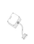
INSTALLING THE HARDWARE
The RAD242 enclosure is an easily-mounted NEMA 4 compliant unit. Outside dimensions
of the enclosure are: 4.53" by 3.54" by 2.17" high. Input/output wiring is sealed by a gland
assembly. The cover is secured to the body by four recessed M-4, stainless steel, captive
screws. Two long M-3.5 x 0.236 screws are provided for mounting the body. Mounting
holes and cover-attaching screws are outside the sealed area to prevent ingress of
moisture and dust. Four threaded bosses inside the enclosure provide for mounting the
printed circuit card assemblies.
Power and Communications Wiring
Electrical power and RS-485 connections to the pod are made internal to the pod on a
removable termination board that plugs into the “personality module” of the RAD unit.
ISO. GND and ISO. PWR :
This is the power connection for the isolated section which may be supplied from the
computer's +12 VDC supply via an extra pair of wires on the RS-485 network or from a
central power supply. To maintain isolation, this power must be independent of “local
power”. The voltage level can be from 7.5 VDC to 23 VDC. (An on-board voltage regulator
regulates the power to +5 VDC.) RAD242 will require only about 40 mA of current and,
thus, any voltage drop of computer power will be inconsequential. If separate power is not
available, then, with some loss of isolation, these terminals can be jumpered to the “local
power” terminals.
RS485+/-:
These are the differential transmit and receive lines for two-wire communications.
EXV: This terminal is for the external voltage level to the inductive suppression diodes
included with the digital outputs. EXV can be as high as 50 VDC.
PWR + and GND: These terminals are used to apply +/-12 VDC power to the pod from a
local power supply. The voltage can be anywhere in the range from 10.5 VDC to 18
VDC. Higher voltage can be used, 24 VDC for example, if an external zener diode
is used to reduce the voltage applied to the RAD242. ( See the Specification section
of this manual to determine the zener diode power rating required.)
Jumpers
There are four jumper locations on the CPU (small) card. Their functions are as follows:
JP1 (adjacent to U22): This jumper will be in the “32K” position and need not
concern you.
JP2 (adjacent to U19), JP3, and JP4 (adjacent to U16):Normally these jumpers
should be in the “ISL”position. If you wish to by-pass the opto-isolators, then
you can move these jumpers to the “/ISL” position.
2-8
Analog-to-Digital Converter Pod
RAD242
User Manual
There are three jumpers on the analog-to-digital card. Their functions are as follows:
JP5 is used to select bias, 2.5 V or ground.
JP6 is used to select the internal 2.5 VDC reference or an external 5VDC
reference. If the internal reference is selected, then the input voltage range
is 0-2.5V or +/-2.5V. If the external 5VDC reference is selected, then the input
voltage range is 0-5V or +/-5V.
JP7 is used to select either Unipolar or Bipolar mode of operation.
2-9
Analog-to-Digital Converter Pod
RAD242
User Manual
SPECIFICATIONS
ANALOG INPUT
Channels:
2 Differential.
Data Coding:
Binary for Unipolar inputs
Offset Binary for Bipolar inputs
Resolution:
Dependent on filter frequency, See Table 1.
Input Voltage Range:
Jumper selectable, 0-2.5V, 0-5V, ±2.5V, ±5V.
Input Impedance:
Varies with input sample rate, 250G?
Programmable Gains:
1, 2, 4, 8, 16, 32, 64, and 128.
Overvoltage:
Continuous single channel, to ±35 V without damage.
DC Input Leakage Current: @ 25°C, 10 pA max.
Temp. Coefficients:
(Note, Recalibration at any temperature or background
calibration will remove drift errors. Due to the thermal
insulation of the NEMA enclosure and internal heating of the
power supply regulators, the actual coefficients are lowered.)
Integral Nonlinearity:
@ 25°C ±0.0015 % of Full Scale Reading Max.
TMIN to TMAX; ±0.0075 % of FSR typical.
Common Mode Rejection Ratio: 100 dB min, at DC.
Normal Mode Rejection at 60 Hz: 100 dB ±0.02 x ƒNOTCH min, for ƒNOTCH of 10,30, 60 Hz.
Common Mode Rejection at 60 Hz: 150 dB ±0.02 x ƒNOTCH min, for ƒNOTCH of 10,30, 60
Hz.
ANALOG OUTPUTS
Compensation Current:
20? A nom., Constant current source for thermocouple cold
junction reference measurements.
DIGITAL INPUTS
Number:
Twelve, on same pins as the output bits, each bit is individually
programmable as either an input or output bit.
Sample Rate: Ports must be polled to read data.
Logic Input Low: -0.5V to +0.8V. Protected to -140 VDC.
3-1
Analog-to-Digital Converter Pod
RAD242
User Manual
Logic Input High: +2.0V to +50.0V. Protected to +200 VDC.
Low-Level Input Current: -450 ? A maximum.
DIGITAL OUTPUTS
Number:
Twelve, on same pins as the input bits, each bit is individually
programmable as either an input or output bit.
Logic-Low Output Current: 350 mA maximum. (See box below.) Inductive suppression
diode included in each circuit.
Maximum allowable current per output bit is 350
mA but, for each eight-bit group, there is a
maximum cumulative total of 650 mA. Output
groups are bits 0-7 and 8-11 (decimal).
High-Level Output Voltage:
Open collector, compliance with up to 50V user
supplied voltage. If no user supplied voltage, outputs
pulled up to +5VDC via 10 K? resistors.
SERIAL COMMUNICATIONS INTERFACE
Serial Port:
Opto-isolated Matlabs type LTC485 transmitter/receiver. Compatible with
RS-485 specification. Up to 32 drivers and receivers allowed on the line.
I/O bus address programmable from 00 to FF hex. Whatever address is
assigned is stored in EEPROM and used as default at next Power-On.
Data Format:
Seven data bits, even parity, one stop bit.
Input Common Mode Voltage:
300V minimum (opto-isolated).
If opto-isolators are by-passed: -7V to +12V.
Receiver Input Sensitivity:
±200 mV, differential input.
Receiver Input Impedance:
12 K? minimum.
Transmitter Output Drive Capability: 60 mA (100 mA short-circuit current capability).
Serial Data Rates: Programmable for 1200, 2400, 4800, 9600, 14400, 19200, 28800,
and 57600 baud. Crystal oscillator provided.
ENVIRONMENTAL
Operating Temperature Range: 0° to 65° C (Optional -40° to +80°) See box (following)
for temperature de-rating based on power supplied.
3-2
Analog-to-Digital Converter Pod
RAD242
User Manual
The power supply voltage level that you use will affect the maximum ambient temperature
that can be tolerated. At higher power levels more heat will be generated by integral
voltage regulators. (For example, when 7.5 VDC is applied, the temperature rise inside
the enclosure is 7.3°C above the ambient temperature.) Thus, maximum ambient
temperature may have to be reduced or de-rated when power supply voltages greater
than 7.5 VDC are used.
The equation to determine temperature de-rating is: VI(TJ = 120) < 22 - TA(in °C)/7
where TA is the ambient temperature and VI(TJ = 120) is the input voltage at which the
voltage regulator junction temperature will rise to the maximum rated temperature of
120°.
For example, at an ambient temperature of 25°, the voltage VI can be up to 18.4V. At an
ambient temperature of 100°F (37.8°C), the voltage VI can be up to 16.6V.
Storage Temperature Range: -50°C to +120°C.
Humidity:
5% to 95% RH non-condensing. Enclosure is designed to meet NEMA4
requirements.
Size: NEMA4 enclosure 4.53" long by 3.54" wide by 2.17" high. (115 mm Long x 90 mm
Wide x 55 mm High)
POWER
Power for the opto-isolated section can be applied from the computer's +12 DC power
supply via the serial communications cable, and from a local power supply for the rest of
the unit.
Opto-Isolated Section: 7.5 to 23 VDC @ 40 mA. (Note: Due to the small amount
of current required, voltage drop in the communication cable is of no
significant consequence.)
Local Power:
+10.5 to +16VDC at 150 mA. (See box that follows.)
-10.5 to -16VDC at 50 mA.
If the local power supply has an output voltage greater than 16VDC, you can install a
Zener diode in series with the supply voltage. The voltage rating of the Zener diode (VZ)
should be equal to VI - 16 where VI is the power supply voltage. The power rating of the
Zener diode should be ? VZ x 0.15 (W). Thus, for example, a 24VDC power supply would
require using an 8.2V Zener diode with a power rating of 8.2 x 0.15 ? 1 W.
3-3
Analog-to-Digital Converter Pod
RAD242
User Manual
INPUT/OUTPUT PIN CONNECTIONS
Input and output connections can be made one of two ways: (a) at Euro style screw
terminals TB1 and, TB2; or (b) at 37-pin, male, sub-D connector J1.
37 Pin D-Sub J1 Pin Connections
Pin Number
1
2
3
4
5
6
7
8
9
10
11
12
13
14
15
16
17
18
19
20
21
22
23
24
25
26
27
28
29
30
31
32
33
34
35
36
37
1
Signal
DI/O0
DI/O1
DI/O2
DI/O3
DI/O4
DI/O5
DI/O6
DI/O7
DI/O8
DI/09
DI/O10
DI/O11
PINT1
AGND
ANOAN1AGND
IOUT
RST
RS485+
RS485PBRST
ISO GND
ISO PWR
GND
EXV+
GND
PWR+
PWRPT0
VEXC+
VEXCAN0+
AGND
AN1+
AGND
AGND
Description
Digital Input/Output Bit 0
Digital Input/Output Bit 1
Digital Input/Output Bit 2
Digital Input/Output Bit 3
Digital Input/Output Bit 4
Digital Input/Output Bit 5
Digital Input/Output Bit 6
Digital Input/Output Bit 7
Digital Input/Output Bit 8
Digital Input/Output Bit 9
Digital Input/Output Bit 10 1
Digital Input/Output Bit 11
User Programmable Interrupt Input 1
Analog Ground
Analog Input 0 ( - )
Analog Input 1 ( - )
Analog Ground
Current Output
System Reset Acknowledge (Negative when PC is Reset)
Positive Transmit & Receive
Negative Transmit & Receive
Processor Board Reset
Ground
Isolated Power Supply In
Ground
Digital Output Clamp Diode Voltage Input
Ground
Power Supply In +
Power Supply In User Programmable Counter/Timer Input
+7.5 VDC Bridge Excitation Output
-7.5 VDC Bridge Excitation Output
Analog Input 0 ( + )
Analog Ground
Analog Input 1 ( + )
Analog Ground
Analog Ground
Use of the User Programmable Inputs require customizing the RAD242 with the RAD
Firmware Development Kit, available separately.
3-4
Analog-to-Digital Converter Pod
RAD242
User Manual
To ensure that there is minimum susceptibility to EMI and minimum radiation, it is
important that there be a positive chassis ground. Also, proper EMI cabling techniques
(cable shield connect to chassis ground at the aperture, twisted pair wires, and, in
extreme cases, ferrite-level EMI protection) must be used.
CE-marked versions of RAD242 meet the requirements of EN50081-1:1992 (Emissions),
EN50082-1:1992 (Immunity), and EN60590:1992 (Safety).
3-5
Analog-to-Digital Converter Pod
RAD242
User Manual
WARRANTY
Prior to shipment, ACCES products are thoroughly inspected and tested to applicable
specifications. However, should equipment failure occur, ACCES assures its customers
that prompt service and support will be available. All equipment originally manufactured
by ACCES which is found to be defective will be repaired or replaced subject to the
following considerations.
TERMS AND CONDITIONS
If a unit is suspected of failure, contact ACCES' Customer Service department. Be
prepared to give the model number, serial number, and a description of the failure
symptom(s). We may suggest some simple tests to confirm the failure. We will assign a
Return Material Authorization (RMA) number which must appear on the outer label of the
return package. All units/components should be properly packed for handling and returned,
freight prepaid, to the ACCES designated Service Center, and will be returned to the
customer's/user's site freight prepaid and invoiced.
COVERAGE
First Three Years: Returned unit/part will be repaired and/or replaced at ACCES option
with no charge for labor or parts not excluded by warranty. Warranty commences with
equipment shipment.
Following Years: Throughout your equipment's lifetime, ACCES stands ready to provide
on-site or in-plant service at reasonable rates similar to those of other manufacturers in the
industry.
EQUIPMENT NOT MANUFACTURED BY ACCES
Equipment provided but not manufactured by ACCES is warranted and will be repaired
according to the terms and conditions of the respective equipment manufacturer's warranty.
GENERAL
Under this Warranty, liability of ACCES is limited to replacing, repairing or issuing credit
(at ACCES discretion) for any products which are proved to be defective during the
warranty period. In no case is ACCES liable for consequential or special damage arising
from use or misuse of our product. The customer is responsible for all charges caused by
modifications or additions to ACCES equipment not approved in writing by ACCES or, if
in ACCES opinion the equipment has been subjected to abnormal use. "Abnormal use" for
purposes of this warranty is defined as any use to which the equipment is exposed other
than that use specified or intended as evidenced by purchase or sales representation.
Other than the above, no other warranty, expressed or implied, shall apply to any and all
such equipment sold or furnished by ACCES.
4-1
Analog-to-Digital Converter Pod
RAD242
User Manual
APPENDIX A
APPLICATION CONSIDERATIONS
INTRODUCTION
Working with RS-422 and RS-485 devices is not much different from working with standard
RS-232 serial devices and these two standards overcome deficiencies in the RS-232
standard. First, the cable length between two RS-232 devices must be short; less than 50
feet at 9600 baud. Second, many RS-232 errors are the result of noise induced on the
cables. The RS-422 standard permits cable lengths up to 5000 feet and, because it
operates in the differential mode, it is more immune to induced noise.
Connections between two RS-422 devices (with CTS ignored) should be as follows:
Device #1
Device #2
Signal
Pin No.
Signal
Pin No.
Gnd
TX+
TXRX+
RX-
7
24
25
12
13
Gnd
RX+
RXTX+
TX-
7
12
13
24
25
A third deficiency of RS-232 is that more than two devices cannot share the same cable.
This is also true for RS-422 but RS-485 offers all the benefits of RS-422 plus allows up to
32 devices to share the same twisted pairs. An exception to the foregoing is that multiple
RS-422 devices can share a single cable if only one will talk and the others will all receive.
BALANCED DIFFERENTIAL SIGNALS
The reason that RS-422 and RS-485 devices can drive longer lines with more noise
immunity than RS-232 devices is that a balanced differential drive method is used. In a
balanced differential system, the voltage produced by the driver appears across a pair of
wires. A balanced line driver will produce a differential voltage from ±2 to ±6 volts across
its output terminals. A balanced line driver can also have an input “enable” signal that
connects the driver to its output terminals. If the “enable signal is OFF, the driver is
disconnected from the transmission line. This disconnected or disabled condition is usually
referred to as the “tristate” condition and represents a high impedance. RS-485 drivers
must have this control capability. RS-422 drivers may have this control but it is not always
required.
A balanced differential line receiver senses the voltage state of the transmission line across
the two signal input lines. If the differential input voltage is greater than +200 mV, the
receiver will provide a specific logic state on its output. If the differential voltage input is
less than -200 mV, the receiver will provide the opposite logic state on its output. A
maximum operating voltage range is from +6V to -6V allows for voltage attenuation that can
occur on long transmission cables.
A-1
Analog-to-Digital Converter Pod
RAD242
User Manual
A maximum common mode voltage rating of ±7V provides good noise immunity from
voltages induced on the twisted pair lines. The signal ground line connection is necessary
in order to keep the common mode voltage within that range. The circuit may operate
without the ground connection but may not be reliable.
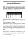
RS-422 Specification Summary
Parameter
Conditions
Driver Output Voltage (unloaded)
Driver Output Voltage (loaded)
L and LDGND
jumpers in
Min.
Max.
4V
-4V
6V
-6V
2V
-2V
Driver Output Resistance
50?
Driver Output Short-Circuit Current
±150 mA
Driver Output Rise Time
10% unit interval
Receiver Sensitivity
±200 mV
Receiver Common Mode Voltage
Range
±7V
4K?
Receiver Input Resistance
To prevent signal reflections in the cable and to improve noise rejection in both the RS-422
and RS-485 mode, the receiver end of the cable should be terminated with a resistance
equal to the characteristic impedance of the cable. (An exception to this is the case where
the line is driven by an RS-422 driver that is never “tri-stated”or disconnected from the line.
In this case, the driver provides a low internal impedance that terminates the line at that
end.)
RS-485 DATA TRANSMISSION
The RS-485 Standard allows a balanced transmission line to be shared in a party-line
mode. As many as 32 driver/receiver pairs can share a two-wire party line network. Many
characteristics of the drivers and receivers are the same as in the RS-422 Standard. One
difference is that the common mode voltage limit is extended and is +12V to -7V. Since any
driver can be disconnected (or tri-stated) from the line, it must withstand this common mode
voltage range while in the tristate condition.
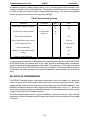
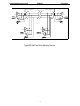
The following illustration shows a typical multidrop or party line network. Note that the
transmission line is terminated on both ends of the line but not at drop points in the middle
of the line.
A-2
Analog-to-Digital Converter Pod
RAD242
Typical RS-485 Two-Wire Multidrop Network
A-3
User Manual