1
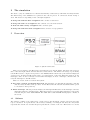
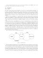
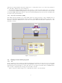
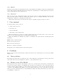
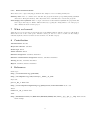
Game of Life, EDA385
Simon Kämpe, [email protected]
Johannes Jakobsson, [email protected]
Bereket Gichamo, [email protected]
October 28, 2009
1
Abstract
The goal of this project was to write a 3D implementation of the classic simulator, Game of Life. Game
of Life is a simulation of cells that live or die depending on their neighbours. To represent the cells a
32 by 32 matrix consisting of 32 integers, were each 32 bit integer represents the 32 bits on the row,
should be used. The matrix is then interpreted by the VGA controller that prints a grid consisting of
red rectangles on a black background on a screen. The simulation was to be done on the Spartan 3E
FPGA with help from external components and the Xilinx design tools.
The external hardware components consists of the VGA controller and the keyboard. In the software
the board layout, keyboard and timer interrupts are handled.
The project has helped us take on a series of hardware and software related problems that we encountered during the course, and helped us to understand the integration between software and hardware
better.
1
Contents
1 Abstract
1
2 The simulation
3
3 Overview
3.1 Software . . . . . . . . . . . . . . . . . . . . . . . . . . . . . . . . . . . . . . . . . . . . . .
3.2 Hardware . . . . . . . . . . . . . . . . . . . . . . . . . . . . . . . . . . . . . . . . . . . . .
3.2.1 The basics of VGA . . . . . . . . . . . . . . . . . . . . . . . . . . . . . . . . . . . .
3
3
4
4
4 Implementation
4.1 Software implementation in C . . .
4.1.1 Interrupts . . . . . . . . . .
4.1.2 Game logic . . . . . . . . .
4.2 Hardware . . . . . . . . . . . . . .
4.2.1 VGA . . . . . . . . . . . . .
4.2.2 Processor Local Bus (PLB)
4.3 Changes from initial proposal . . .
4.3.1 3D . . . . . . . . . . . . . .
4.3.2 Ruleset . . . . . . . . . . .
4.3.3 Keyboard . . . . . . . . . .
5
5
5
5
6
6
7
7
7
8
8
.
.
.
.
.
.
.
.
.
.
.
.
.
.
.
.
.
.
.
.
.
.
.
.
.
.
.
.
.
.
.
.
.
.
.
.
.
.
.
.
.
.
.
.
.
.
.
.
.
.
.
.
.
.
.
.
.
.
.
.
.
.
.
.
.
.
.
.
.
.
.
.
.
.
.
.
.
.
.
.
.
.
.
.
.
.
.
.
.
.
.
.
.
.
.
.
.
.
.
.
.
.
.
.
.
.
.
.
.
.
.
.
.
.
.
.
.
.
.
.
.
.
.
.
.
.
.
.
.
.
.
.
.
.
.
.
.
.
.
.
.
.
.
.
.
.
.
.
.
.
.
.
.
.
.
.
.
.
.
.
.
.
.
.
.
.
.
.
.
.
.
.
.
.
.
.
.
.
.
.
.
.
.
.
.
.
.
.
.
.
.
.
.
.
.
.
.
.
.
.
.
.
.
.
.
.
.
.
.
.
.
.
.
.
.
.
.
.
.
.
.
.
.
.
.
.
.
.
.
.
.
.
.
.
.
.
.
.
.
.
.
.
.
.
.
.
.
.
.
.
.
.
.
.
.
.
.
.
.
.
.
.
.
.
.
.
.
.
.
.
.
.
.
.
.
.
.
.
.
.
.
.
.
.
.
.
.
.
.
.
.
.
.
.
.
.
.
.
.
.
.
.
.
.
.
.
.
.
.
.
5 User manual
8
6 Problems
6.1 Timer problems . . . . . . . . . . . . . . . . . . . . . . . . . . . . . . . . . . . . . . . . . .
6.2 Writing to the VGA BRAM . . . . . . . . . . . . . . . . . . . . . . . . . . . . . . . . . . .
6.2.1 Xilinx Platform Studio . . . . . . . . . . . . . . . . . . . . . . . . . . . . . . . . . .
8
8
8
9
7 What we learned
9
8 Contribution
9
9 References
9
2
2
The simulation
The Game of Life is a simulation of cells that was initially constructed by John Horton Conway in 1970.
The initial setup of the simulation is a grid were the cells are placed. A cell has two modes: living or
dead. The states are depending on the cells eight neighbors:
A living cell with less than 2 neighbors The cell dies of starvation.
A living cell with 2 or 3 neighbors The cell lives on to the next iteration.
A dead cell with exactly 3 neighbors The cell lives again.
A living cell with more than 3 neighbors The cell dies of overpopulation.
3
Overview
Figure 1: System architecture
There are two inputs to the Microblaze; the PS2 keyboard, and the Timer. The keyboard is responsible of the user input, which descides what the sofware will do. The Timer is in charge of periodically
tell the Microblaze to output a new picture to the BRAM, which is then read by the VGA and displayed
on the screen. To make the Microblaze aware of a new keypress, or that the Timer has expired, we use
interrupts. Since we use both keyboard and timer interrupts, we need a interrupt controller that can
relay the interrupts to the Microblaze.
There are 2 basic chain of events in the system:
A user press a button on the PS2 keyboard: The interrupt goes through the interrupt controller
and after that, the Microblaze processor. In the Microblaze the software determineis what option
to executed for the specific key.
A Timer interrupt: Like the previous example, the interrupt will first arrive at the interrupt controller,
which then sends it to the Microblaze. When the software recievs the Timer interrupt a new picture
is drawn and put on the VGAs BRAM. The VGA will read the BRAM and display its contents on
the screen.
3.1
Software
The software consists of two main parts; a setup part for the interrupts, and the part were the game
logic is calculated. To represent the cells an array consisting of 32 integers was used, the array index
represents the current row and the integers represents the content of the row. Microblaze is a 32 bits
3
CPU which means that integers are 32 bits long. We used this in our representation by making each bit
in the integers representing a single cell, if the bit is 1 the cell is alive, if it is 0 the cell is dead.
3.2
Hardware
Number of Slices 1807 out of 8672 20%
Number of Slice Flip Flops 2064 out of 17344 11%
Number of 4 input LUTs 2863 out of 17344 16%
Number used as logic 2517
Number used as Shift registers 90
Number used as RAMs 256
Number of IOs 19
Number of bonded IOBs 19 out of 250 7%
Number of BRAMs 17 out of 28 60%
Number of MULT18X18SIOs 3 out of 28 10%
Number of GCLKs 1 out of 24 4%
Number of DCMs 1 out of 8 12%
The custom hardware for the VGA controller is written in VHDL to be specialized to our needs.
Since we do not need to make a VGA controller that can be implemented on other projects, we could
make it smaller and simpler.
3.2.1
The basics of VGA
VGA basically stands for Video Graphics Array and it shows either an analog computer display standard,
the 15- pin D-subminiature VGA connector, or the 640x480 resolution itself. It is implemented as a single
chip (an ASIC) for which reason it is called Array instead of adapter. And most PC clone manufacturers
have taken VGA as the lowest common denominator of PC graphics hardware support. Things which are
included in VGA specification include video RAM, color modes and color palette, pixel clock, maximum
horizontal pixels, maximum lines of pixels, refresh rates,etc. The graphical information that is intended
to be drawn in the VGA monitor is sent via DB-15 connector which is also often termed as VGA display
port.
When using Spartan 3E FPGA to control the graphics that is displayed in the VGA monitor, a custom
hardware should be written in VHDL that drives the five signals namely VGA_RED, VGA_GREEN,
VGA_BLUE, HSYNC and VSYNC via resistors. The first three signals determine the RGB value of a
pixel while the later two control the horizontal and the vertical synchronization the pixel drawing. The
VGA_RED and VGA_GREEN comprise of three bits each while VGA_BLUE is made of 2 bits which
completes 8-bit VGA display with 28 = 256colordisplay.
The drawing of pixels in the CRT or LCD screen is carried out in pixel by pixel basis horizontally
from left to right and vertically from top to bottom. VGA controller dictates a resolution by producing
timing signals to control raster patterns. Modern VGA displays support multiple display resolutions.
The video data is taken from the ram to assign bits to each pixel location. The Spartan- 3E board uses
8 bits per pixel, producing one of the 256 colors. As the pixel drawing in the display continues the VGA
controller indexes into the video data buffer. The VGA controller uses the horizontal and vertical sync
timing signals to coordinate the delivery of the video data on each pixel clock. The VS signal defines
the refresh frequency of the display or the frequency at which all information on the display is redrawn
which is in the range of 60 to 120 Hz range.
4
4
Implementation
As described before, the software part is run on the Microblaze and communicates with the FPGA
implemented VGA and BRAM via the PLB. To send new pictures to the VGA from the software, we
first stores the picture on the BRAM, that later can be read by the VGA.
4.1
Software implementation in C
Figure 2: Software flowchart
The software consists of two main parts: Interrupts and Game logic. Game logic is the main part of
all the game rules and memory access, and is thus responsible for writing to the BRAM. The interrupt
section handles interrupts and handlers for the keyboard and the timer, and is called every time a
interrupt occurs. The keyboard handler sets different options for the simulation, and the timer handler
calls the game logic, depending on the options.
4.1.1
Interrupts
In the startup phase of the software the interrupts for the keyboard and timer are initialized together
with the specified options. To handle the interrupts from the keyboard and timer to the processor we
had to use a interrupt controller so that the processor could read both interrupts on one port. The
interesting part of the interrupt logic is the handler that takes care of the interrupts.
The keyboard handler recievs the buffer containing the key codes and saves the key for the timer
interrupt.
The handler for the timer takes the saved key from the keyboard handler and sends it to a function
that either pauses the game, tells the game logic to calculate the next iteration, or change the speed of
the timer interrupts. By changing the timer interrupts we can control how fast the game should render
a new matrix for the VGA to put on the display.
4.1.2
Game logic
The game logic handles the calculation of the cells on the 32 by 32 board, and outputs the new cell
layout to the BRAM on the VGA controller.
5
To save bandwith and memory space, the cell layout that is written to the BRAM is only a 32 bit
binary number that represents one row in the 32 by 32 grid.
4.2
4.2.1
Hardware
VGA
Our VGA controller using Spartan 3E FPGA is a custom IP core written in VHDL. The VHDL code
is based on the example Monochrome VGA controller given in the course home page from which the
parameters dictating the resolution and refresh rate are taken as they are presented in that document.
The processes used for the generation of VS and HS are also taken as they are. The major deviation
from the example design is in the use of PLB bus instead of OPB which subsequently affected all bus
related parameters. Calculation of pixel clock from the PLB bus clock was also a modification from the
OPB one.
The use of dual port BRAM as a component in VGA controller in a similar manner as given in the
example code was pursued as the best implementation of video buffer. In this arrangement the RAM
memory was initialized to accommodate the necessary bits information that was required to show the
whole 32 x 32 grid at the VGA monitor. The buffer was meant to write to and read from it a word at
a time. And the read word was meant to determine a visibility of each cell in a row in the rectangular
grid.
Even though, the use of such BRAM was so perfect for our implementation of VGA controller, its
integration to the software was not smooth and successful for the reasons mentioned under the section
6. So we had to turn our face to the other model of BRAM, single port BRAM. This BRAM was added
as a user memory space while generating the IP core and it was better model in a sense we need not
care about the bus parameters. However, we had to redesign our implementation of the VGA controller
in relation of BRAM. The main points of the modification were due to the fact that in the single port
BRAM we could only read a byte at a time as opposed to a word at a time in the dual one; and primarily
for the two models follow different coding styles (dual as a component while in the single as a separate
process) that required some more work on resynchronization. The amount of time that was require was
significant especially as we turned to the latter model in final moments for we did not lost confidence in
the previous method till the last minute.
The second model is depicted schematically as follows:
Figure 3: VGA flowchart
The grid drawing was handled in a process in VHDL. This process is designed to draw a grid of
desired size which is determined by hard coding the start and end of the drawing, and the desired length
of each cell. Our size of interest for the grid was 32 i.e. 32 by 32 grid with the size length of each cell 10
pixels. Then what the process does is determining the visibility of each pixel based on the representative
bit read from the BRAM. A bit from the read word may also represent more than one pixel in the grid
depending on the specified length of each cell i.e. if the length of a cell is 1 pixel then a bit represents
only a pixel, if two then two vertically consecutive pixels. Hence a read word will determine the visibility
of pixels in a row of the rectangular grid. The drawing of the whole grid with living cells made visible
6
while the dead kept invisible takes the refresh rate i.e. if the game is set to be so fast, new patterns of
the cells will be displayed at every refresh rate.
An alternative grid rendering way that was explored to realize the same design was to use bitmap
of a cell saved in a ROM and displaying it in an appropriate place on the screen based on the bit value
read from BRAM. This method was not chosen for the final implementation as it was not as flexible and
as easier as the previous method.
4.2.2
Processor Local Bus (PLB)
The PLB being used in this project is the PLB version 4.6, and is in charge of data communication on
the board. The PLB is used when the software writes to the BRAM through the VGA controller, by the
interrupt controllers communication to the CPU, and by the keyboard and timer comunication to the
interrupt controller.
Figure 4: System layout
4.3
4.3.1
Changes from initial proposal
3D
In the original proposal we wanted to make the simulation in 3D instead of 2D, but choose to stick with
the 2D model. The reasons for this is that we had planned to move over to 3D once we got the complete
system integrated and working on a 2D basis. Since we encountered problems with our BRAM, there
was not time to implement the 3D support in the VGA controller.
There is however software support for calculating the grid in a 3D environment.
7
4.3.2
Ruleset
Initially we had planned to implement the rules of the simulation in VHDL, but instead we implemented
it in C. The reason for this is that the speed benefit from calculating the board in hardware is not needed,
and the implementation is far simpler in C.
4.3.3
Keyboard
Since the project is not implemented with a 3D view, the option of camera angles that was proposed
was not needed anymore. Instead of having the planned option of changing individual cells, we have
implemented a function to randomize the entire grid.
Other functions that has been added is the options of pausing, stepping and speed control.
5
User manual
To run the Game of Life you need:
1. VGA connected screen
2. PS2 keyboard
3. Spartan 3E 1200
4. The Game of Life download.bit
When the hardware is connected, and the download.bit has been downloaded to the board via the
Export tool, the game should start executing without further help.
While the simulation is running it is possible to manipulate the game with the following keys:(Case
insensitive)
Space Pause or start the game.
A Increase the game speed.
Z Decrease the game speed.
R Create a random cell matrix.
S Stepping option. Displays next iteration then pauses.
6
Problems
Many of the problems and slowdowns originated from the lack of knowledge we had about the Xilinx
design tools.
6.1
Timer problems
We initially had some timer problems were the counter didnt give any interrupts at the specified reset
value. This was solved by changing the counter to count down instead of up.
6.2
Writing to the VGA BRAM
The integration of the software and hardware caused a lot of stalls in the development, particularly the
part were the software writes to the BRAM. The problem of not getting the correct bit pattern was in
both the software and the VHDL code. The software part was due to a error were the data was sent via
a pointer to the BRAM. In the VHDL code the problem was that just a part of the whole 32 bit word
was read correctly. This was fixed by compromising the design, and change the memory type from a two
port BRAM to a single one.
8
6.2.1
Xilinx Platform Studio
There has been a couple annoying problems in the design tool we been using, mainly two:
Memory leak A not to common error was that the program would stop responding during synthesis
and start to fill up the memory. The only solution we could find was to restart the program.
Increasingly slow synthesis After a couple of iterations of the hardware synthesis the program would
take longer and longer to finish. This was fixed by copying the changed files to an older project
and continue the work on that project.
7
What we learned
After the project we feel more secure in the use of the Xilinx software and the creation of custom IP’s,
which also is one of the course goals. Another course goal was to be able to realize our idea using a
embedded system, and we feel that we have learned a lot in this category.
8
Contribution
VGA hardware Bereket
Keyboard software Johannes
Game logic Simon
Timer software Simon
Software integration Johannes and Simon
Software and hardware integration Bereket, Johannes and Simon
Testing Bereket, Johannes and Simon
Report Johannes, Bereket and Simon
9
References
Game logic:
http://www.bitstorm.org/gameoflife/
http://en.wikipedia.org/wiki/Conway’s_Game_of_Life
Keyboard:
ps2 v1_00_a Xilinx API
http://www.computer-engineering.org/ps2keyboard/scancodes2.html Scan codes
Timer:
tmrctr v1_10_b Xilinx API
VGA:
http://fileadmin.cs.lth.se/cs/Education/EDA385/HT06/doc/mono_vga_xps_7_1.zip Monochrome
VGA example
9