1
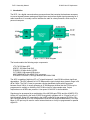
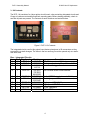
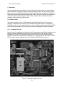
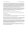
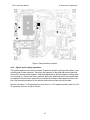
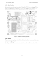
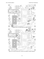
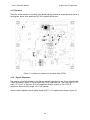
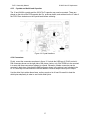
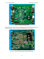
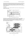
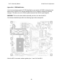
DCP-1 Assembly Manual
DCP-1 Assembly Manual
© 2005 John B. Stephensen
1. Introduction
The DCP-1 is a digital communications processor board that contains the hardware necessary
to convert signals between analog and digital forms and perform digital signal processing for a
radio transceiver. It is usually used to interface the radio to a host processor, which may be a
personal computer.
Figure 1. DCP-1 Block Diagram
The board contains the following major components:
LTC1746 25 Msps ADC
AD9767 125 Msps Dual DAC
PCM3501 26 ksps Audio CODEC
CY7C68001 High-speed USB device
ML67Q5003 MCU with ARM7 RISC processor
XC3S400 FPGA with 6,144 logic elements and 288 k RAM
The ADC is capable of digitizing RF or IF signals between 0.1 and 50 MHz without significant
degradation. The ADC operates at 24.576 Msps and the typical single-tone dynamic range is 94
dB at 5 MHz. The DAC is used to generate complex baseband signals with frequencies
between 0 and 3 MHz. It usually operates at 12.288 Msps per channel but the FPGA may be
programmed to multiply or divide the 24.576 MHz clock for other sample rates. Output
frequencies over 40 MHz are possible. A low-speed 10-bit ADC is also available.
Signals may be processed by a combination of the 400,000-gate FPGA and the 48 MIPS CPU.
Analog I/O is provided by the audio CODEC that typically operates at 8 or 12 ksps for a 3 or 5
kHz bandwidth. Digital I/O is provided by the UART on the MCU that supports RS-232 or RS485 communication at up to 230.4 kbps and the USB SIE that supports data rates of 12 or 480
Mbps. A SPI port may be used to control external devices or it may be programmed for parallel
digital I/O.
2
DCP-1 Assembly Manual
© 2005 John B. Stephensen
2. Required Tools
Assembly of PC boards with surface mount technology requires special tools. The first
requirement is a static-free workstation. This can be a static-dissipative mat on the top of a desk
with a wrist-strap connecting the user to the mat. 3M and other companies make inexpensive
mats and straps intended for field service. These are available through distributors such as
Mouser and Digi-Key and orders may be placed via the Internet. The mat should be connected
to ground. Use the third wire of the AC outlet powering the soldering iron after you have tested
that it is wired correctly. Required tools are:
Static-dissipative work surface
Wrist strap for grounding user
Temperature-controlled soldering iron with grounded tip
0.01-0.015” diameter soldering tip
1/16-1/8” chisel-shaped soldering tip
Soldering tip cleaner
Hot air pencil (optional)
Vacuum pick-up tool
Tweezers (metal or other conductive material)
X-acto (or equivalent) knife
Probe for positioning components (toothpicks or Orange Sticks)
1/32” width solder-wick (no-clean flux preferred)
0.015-0.020” diameter 63/37 alloy wire solder with no-clean flux
63/37 alloy solder paste with no-clean flux
Solder paste dispenser (syringe)
Two 25-60 W work lights
5-7 X magnifier
A good soldering iron with fine tips that have been recently cleaned is a must. Set the
temperature to 650 F for 63/37 solder. Two irons are useful to avoid tip changes and to remove
0805 (0.08” x 0.05”) to 1210 (0.12” x 0.10”) package SMT parts. A hot-air pencil is useful for
mounting the SSOP and QFP ICs but is not mandatory.
Tweezers are useful for placing small parts and a hand-operated or electric vacuum pick-up tool
is helpful for placing the quad flat packs. Pick-up tools are available from the same distributors
that handle static control mats. Orange sticks are wooden sticks (orange wood is anti-static)
with a chisel tip at each end. They work better than toothpicks for pushing and holding 0805 to
1210 size components.
As very little solder paste is required, purchase a small quantity in a syringe. Use a 27 gauge or
slightly larger needle. Plungers are hard to operate, so a gun that takes syringes is a useful
investment if more SMT work is anticipated.
Excellent magnifiers are available from horological (watchmaker) supply companies or from
electronic assembly supply distributors such as Contact East or Techni-Tool. Solder and staticfree mats are also available from these sources. Make sure that adequate lighting is available,
as more is required as magnification increases. Two or more light sources are useful as this
minimizes shadows.
Warning: This is not a kit for beginners. The assembler should have experience soldering
surface mount components. Previous experience with a simpler SMT kit is recommended.
3
DCP-1 Assembly Manual
© 2005 John B. Stephensen
3. Kit Contents
The DCP-1 kit consists of a 4-layer printer circuit board, a box containing integrated circuits and
6 bags of surface mount and through-hole mounting parts. Before starting assembly, check to
see that all parts are present. The contents of each container are itemized below.
Figure 2. DCP-1 Kit Contents
The integrated circuits used in this project have feature sizes down to 90 nanometers so they
are sensitive to static charges. The items in the box and bag 3 must be opened only at a staticfree work area.
Box – Integrated Circuits
Item Qty. Pkg./Leads
Marking
1
1
SOIC 8
ADM348
2
1
SOIC 8
MCP6022
3
1
SOIC 14
AHC14
LVC14
4
1
SOIC 20
55C3223
75C3223
MAX3223
5
1
SSOP 20
PCM3201E
6
1
QFP 48
9767AST
9767ASZ
7
1
SSOP 48
LTC1746
8
1
SSOP 56
CY7C68001
9
1
QFP 144
XC3S400
10
1
QFP 144
L67Q5003
Description
RS-485 transceiver, half-duplex
Dual operational amplifier, rail-to-rail I/O
Hex schmidt-trigger inverter
RS-232 dual driver & dual receiver
Audio CODEC, single channel, 8-24 ksps
Dual high-speed DAC
High-speed ADC, 25 Msps max.
High-speed USB SIE
FPGA, Spartan-3
MCU, ARM7
4
DCP-1 Assembly Manual
© 2005 John B. Stephensen
Bag #1 – Connectors and Heat Sinks
Item Qty.
Description
1
1
Connector, USB type A
2
1
Connector, USB type B
3
2
Connector, RJ-45 (one or both with 2 LEDs)
4
1
Connector, Mini-DIN, 8 pin
5
1
Connector, dual 1/8” phone jack
6
1
Connector, 5 25-mil pins, 100-mil centers, locking ramp
7
1
Heat sink, 2 holes, appx. 0.75” x 1.5”
8
1
Heat sink, appx. 0.6” square
9
1
Thermal tape, appx. 0.5” square
10
1
Socket, 8-pin DIP
11
1
Header, 20-pin dual row, 25-mil square pins, 100-mil centers
12
2
Screw, 6-32 x 3/8”
13
2
Lock washer, internal tooth, #6
14
2
Hexagonal nut, 6-32
Bag #2 – Crystals and Thru-hole Regulator
Item Qty.
Description
1
1
Crystal, HC-49/U, 24.000 MHz +/-100 PPM
2
1
Crystal, HC-49/U or SMT, 6.000 MHz +/-100 PPM
3
1
LDO VR, adjustable, 3A, TO-220 (IRU1030 or equiv.)
4
1
Insulator, HC-49/U
Bag #3 - Semiconductors
Item Qty. Pkg./Leads
1
1
SOT-23 3
2
1
SOT-23 3
3
1
SOT-23 3
4
1
SOT-23 3
5
6
1
1
SOT-23 5
SOT-23 6
7
1
SOT-223
8
1
5 x 7 mm
Marking
5H
BC
Z4
SL
PL
9T
CU4
D33AB
1117
CWX815
24.57M
Description
Small-signal diode (MMBD4148 or equiv.)
3.9 V zener diode
6.2 V zener diode
3.15 V voltage monitor
Dual NPN transistor array, XN0121100L
Dual unbuffered inverter,
SN74LVC2GU04DBV
LDO VR, adjustable, 500 mA
(LT1117 or equiv.)
Oscillator, 5 x 7 mm SMT, 5V
24.576 MHz +/-25 PPM
5
DCP-1 Assembly Manual
Bag #4 - Capacitors
Item Qty.
Package
1
3
0805
1
4
0805
2
2
0805
2
2
0805
3
3
0805
4
8
0808
5
62
0805
6
4
0805
7
1
0805
8
11
1206
3216
9
7
3216
10
1
cylindrical
© 2005 John B. Stephensen
Marking
None
None
None
none
None
none
none
none
none
none or
475
106
JJ7
220-470 uF
Bag #5 - Inductors/Transformers
Item Qty.
Package
Marking
1
1
SMT 5-ld.
None
2
2
0805
None
3
3
1210
3R9
4R7
Description
Capacitor, 10 pF +/-10% 50V ceramic
Capacitor, 27 pF +/- 5% 50V ceramic
Capacitor, 56 pF +/-5% 50V ceramic
Capacitor, 470 pF +/-5% 50V ceramic
Capacitor, 4700 pF +/-5% 50V ceramic
Capacitor, 0.01 uF +20/-80% 25V ceramic
Capacitor, 0.1 uF +80/-20% 16 V ceramic
Capacitor, 1 uF +80/-20% 16 V ceramic
Capacitor, 4.7 uF +80/-20% 16 V ceramic
Capacitor, 4.7 uF +80/-20% 16 V ceramic
or tantalum
Capacitor, 10-22 uF +80/-20% 6 V
tantalum
Capacitor, 220-470 uF, 6V, aluminum
electrolytic
Description
Transformer, 50-ohm to 200-ohm CT
Inductor, 0.56 uH +/-5%
Inductor, 3.9 or 4.7 uH +/-20%
6
DCP-1 Assembly Manual
Bag #6 - Resistors
Item Qty.
Package
1
6
0805
2
3
5
19
0805
0805
4
1
0805
5
4
0805
6
1
0805
7
3
0805
8
1
0805
9
10
6
2
0805
0805
11
19
0805
12
2
0805
13
2
0805
© 2005 John B. Stephensen
Marking
240
24R9
49R9
101
100R
201
200R
301
300R
621
604R
102
1001
202
2001
4991
822
8251
104
1002
563
5632
104
1003
Description
Resistor, 24 ohm +/-5%
Resistor, 49.9 ohm +/-5%
Resistor, 100 ohm +/-5%
Resistor, 200-ohm +/-5%
Resistor, 300 ohm +/-5%
Resistor, 620 ohm +/-5%
Resistor, 1,000 ohm +/-5%
Resistor, 2,000 ohm +/-5%
Resistor, 4,990 ohm +/1%
Resistor, 8,200 ohm +/-5%
Resistor, 10,000 ohm +/-5%
Resistor, 56,000 ohm +/-5%
Resistor, 100,000 ohms +/-5%
Note that the integrated circuits and resistors are marked as shown in the parts list, above. The
capacitors are unmarked so be careful to keep the different values separated. Some of the
inductors are marked and some aren’t but they can be differentiated based on size.
7
DCP-1 Assembly Manual
© 2005 John B. Stephensen
4. Assembly
We recommend doing hand assembly of this kit in the steps outlines below to ensure that all
parts are placed in the proper locations and that soldering is eased. Be very careful to place
parts in the correct location and observe polarities on the surface mount parts. It is difficult to
remove and remount parts without damaging the PCB so take time to ensure that assembly is
correct the first time. Always inspect work for solder bridges and cold solder joints during
assembly as this minimizes problems later.
4.1 IC Side of PCB
The board is wired for use of a 6 MHz crystal to regulate the MCU clock. This causes no
problems in applications (such as the UHF OFDM modem) where the ADC is sampling at
12.288 Msps, as it is hear a Nyquist frequency. If your application requires sampling at 24.576
MHz and signals present at 6 MHz could be a problem, see appendix A before proceeding.
4.1.1
Integrated Circuits
Mount the ten ICs contained in the black box first. These are the most difficult to solder and the
process would be hindered by the presence of other components. Start with the 144-pin
packages (MCU and FPGA) and then mount the other ICs in any order. Double-check the
alignment on each part carefully before soldering. Pin 1 must line up with the number 1 on the
PCB as shown in the photograph below. Note that the USB SIE label shows pin 1.
Figure 3. Mounting Integrated Circuits
8
DCP-1 Assembly Manual
© 2005 John B. Stephensen
The components with 0.5-0.65 mm lead spacing (FPGA, MCU, ADC, DAC and CODEC) should
be mounted using solder paste. Dispense the paste in a thin (5-10 mil) strip across the PCB
mounting pads for each package before it is mounted. Then place the part and align it with the
pads. If the paste is spread out past the pad ends, wipe off the solder with a swab and reapply.
Use a 5-7X magnifier to check the alignment of the pins with the pads and then solder the four
corner pins using a soldering iron with a 0.01-0.02” diameter tip. Recheck the alignment after
each soldering operation and reheat the joint and move the part if necessary.
After the corner pins are soldered, solder the remaining pins. A hot-air pencil is the easiest but a
soldering iron will do. When using the iron, it is best to place it between pins so that all solder is
heated and flows to the pads. After soldering all pins, use thin (1/32”) solder-wick to remove
excess solder. Then carefully check every pin and the spaces between pads using the
magnifier. Use the solder-wick to clean up any shorts.
Note: If the mini-DIN connector is not to be used, leave out the 74AHC14 IC.
There are a lot of pins to solder so take time to do this correctly. Solder each package before
mounting the next.
4.1.2
Other Semiconductors
If you have Rev. D of the PCB, mount a jumper wire between the pads as shown in the diagram.
This jumper is near the lower left corner of the oscillator (item 8).
Mount the components in bag 3 as shown in the diagram below. The oscillator must be mounted
using solder paste but the other components can be attached with wire or paste solder. Mount
the oscillator first. Note that item 7 will be added later to the other side of the PCB.
Apply paste solder to the four pads and then place the crystal oscillator on the pads, observing
proper polarity. Pin 1 is marked by a cutout on the pad on the bottom of the package or a dot on
the top of the package. Heat each pad near the oscillator with the soldering iron until the solder
bonds to the oscillator. Proper bonding is verified by seeing that solder flows into the crevasses
above each mounting pad on the oscillator package.
Now mount the other components. All will mount only one way, except the 6-pin SOT-23
package. Its polarity is determined by the printing on the package. Pin 1 is in the lower left-hand
corner when the printing is right side up.
9
DCP-1 Assembly Manual
© 2005 John B. Stephensen
Figure 4. Semiconductor locations.
4.2.2
Bypass and Coupling Capacitors
The bypass capacitors can now be mounted. Prepare the board by placing a little solder on one
mounting pad for each capacitor. Then place the capacitor on the pads and heat the pad with
solder until it flows onto the capacitor. Hold the capacitor down with a toothpick or Orange Stick
or it will stand up. After the first end is soldered, apply wire solder and heat to the opposite pad
to complete the connections. Inspect the connections and reheat if either appears to be a cold
joint. Use the same procedure for the resistors and inductors when they are mounted.
Mount the fourteen 0.1 uF capacitors first, then the four 4.7 uF capacitors and the three 10 or 22
uF capacitors as shown in figures 5 and 6.
10
DCP-1 Assembly Manual
© 2005 John B. Stephensen
Figure 5. Mount 15 0.1 uF capacitors.
Figure 6. Mount three 22 uF, five 4.7 uF (1210) and one 4.7 uF (0805) capacitors.
11
DCP-1 Assembly Manual
4.2.3
© 2005 John B. Stephensen
Other Capacitors
Next, mount the remaining capacitors on the IC side of the PCB. These consists of a 470 three
10 and two 56 pF capacitors near the ADC, 2 each 27 pF capacitors near the USB SIE and
MCU and a 470 pF and three 4700 pF capacitors near the CODEC, as shown below.
Figure 7. Locations of remaining capacitors.
4.2.4
Resistors
There are a number of resistors on the IC side of the board and these are mounted in two steps
as shown in the figures 8 and 9.
Note: If the mini-DIN SPI connector is not used, don’t mount the six 100-ohm resistors in the
lower left-hand corner.
12
DCP-1 Assembly Manual
© 2005 John B. Stephensen
Figure 8. 100, 10 K and 100 K ohm resistor locations.
Figure 9. 24, 49.9, 200, 300, 620, 4.99 K, 8.2 K and 56 K resistor locations.
13
DCP-1 Assembly Manual
4.2.5
© 2005 John B. Stephensen
Inductors
There are 4 inductors and one transformer to mount on the IC side of the PCB. The two 0.56 uH
inductors are the smallest and are not marked. The 2 larger 3.9 or 4.7 uH inductors should be
marked bur are distinguishable by size. The transformer is a surface-mount device with 5 solder
pads on the bottom. Be careful to orient it correctly on the PCB. The side with 3 pads is oriented
towards the upper part of the drawing. This matches the mounting pads.
Figure 10. Locations of inductors and transformer.
4.3 Connector Side
Now that the IC side is complete, turn the PCB over and start on the connector side of the
board. It will be necessary to use a board holder or to mount spacers in the holes in the 4
corners of the board to prevent it from wobbling during assembly. If you are using preheating
during assembly, a hot air bath is required, as a hot plate will not conduct enough heat to the
proper side of the PCB.
14
DCP-1 Assembly Manual
© 2005 John B. Stephensen
4.3.1 Resistors
There are a few resistors on this side of the board and they should be mounted first as shown in
the diagram, below. Also attach the SOT-223 regulator at this time.
Figure 11. Locations of resistors on connector side of PCB.
4.3.2
Bypass Capacitors
The majority of the components on this side are bypass capacitors for the ICs on the other side.
These are shown in figure 12. Mount all but the 0.1-uF capacitors first. There are eight 0.01 uF,
eight 1 uF, six 4.7 uF and four 10-22 uF capacitors. Observe polarity on the 10-22 uF
capacitors. Also mount the single 3.9-4.7 uH inductor.
After the other capacitors are mounted, install the 47 0.1 uF capacitors as shown in figure 13.
15
DCP-1 Assembly Manual
© 2005 John B. Stephensen
Figure 12. Capacitor locations.
Figure 13. 0.1 uF capacitor locations.
16
DCP-1 Assembly Manual
4.3.3
© 2005 John B. Stephensen
Crystals and Axial Lead Capacitor
The 12 and 24 MHz crystals and the 220-470 uF capacitor may now be mounted. These are
placed on the side of the PCB opposite the ICs, as shown below, and soldered on the IC side of
the PCB. Place insulators on the crystal leads before soldering.
Figure 14. Crystal locations.
4.3.4 Connectors
Finally, mount the connectors as shown in figure 15. Include the USB type A, RJ-45 and miniDIN connectors shown on the right side of the picture, below, only if the PCBA is to be mounted
in a case with those connectors adjacent to a panel. Otherwise, header connectors can be
mounted in their place. Note that the SMB connector shown in the picture is not included in the
kit. It is normally not connected but could be added to create a sample clock input or output.
Use the chisel tip to solder these items, as they require a lot of heat. Be careful to heat the
shield pins adequately in order to avoid cold solder joints.
17
DCP-1 Assembly Manual
© 2005 John B. Stephensen
Figure 15. Connectors mounted to PCB.
After mounting the connectors, add the U-shaped heat sink and TO-220 voltage regulator and
solder the three pins. Use the 6-32 screws, lock washers and nuts for mounting.
Figure 16. IC side of PCB showing heat sink and voltage regulator.
18
DCP-1 Assembly Manual
© 2005 John B. Stephensen
Now that all parts are soldered, add the square heat sink with an array of fins to the FPGA. It is
attached with the square adhesive pad included in the same bag as the heat sink. Remove the
protective paper from one side of the tape and apply it to the bottom of the heat sink then
remove the paper on the other side and press the heat sink onto the FPGA. This completes the
assembly of the basic kit.
4.2.5 Options
If a sample clock connector is added to the PCBA, it can be wired in by adding components to
the board as shown below.
Figure 17. External sample clock connector.
Note that there are unused pads near the ADC and DAC. These are for user-supplied
components to implement low-pass filters for a particular application. The DAC pads are shorted
through so the output is usable external with filters. The ADC pads are supplied for
implementation of low-pass or band-pass filters. If no user-supplied filter is to be used, mount
two 0.1 uF capacitors where noted below.
Figure 18. ADC and DAC filter locations.
19
DCP-1 Assembly Manual
© 2005 John B. Stephensen
There are also pads for 3 and 5 pin header connectors for the ADC and DAC, respectively. If
the PCB is to be mounted in a box with analog circuitry, these headers can be installed in place
of the USB and RJ-45 connectors. If the mini-DIN SPI connector and 74AHC14 buffer aren’t
needed, there is a spot for a 7-pin SPI connector at the bottom of the board.
By default, the board is configured for use with the internal boot ROM. To boot from flash
memory after it is programmed, install a jumper (or 0-100-ohm resistor) at the location labeled
FLASH underneath the MCU.
4.4 Inspection and Power-up
Carefully inspect the PCB assembly for solder bridges, foreign material and reversed tantalum
or aluminum electrolytic capacitors before applying power. Then check the power connector
with an ohmmeter. The resistance should be above 500 ohms for both power supply inputs.
Then check the 1.3 and 2.5 volts supply distribution. The resistance should be above 2000
ohms. The 2.5 V-supply may be accessed at the tab of the voltage regulator on the connector
side of the board. The 1.2V supply is accessible near the heat sink on the regulator on the IC
side of the board. Clear any shorts before applying power.
Always apply power 3.3V and 5V to the board simultaneously to prevent any damage to the
analog ICs. Apply power for a short time and check all voltages to ensure that they are within +/5%. Then apply power for 10 minutes and check the voltages again. If any voltages are low,
check for abnormal heating of components and clear the problem before proceeding.
20
DCP-1 Assembly Manual
5
© 2005 John B. Stephensen
Programming
To program the MCU flash memory a program provided by Oki Semiconductor is required. This
software is only available for Windows. It may be download from their web site at
www2.okisemi.com by clicking on “Oki In System Flash Programming (ISFP) Utility”. Download
the program and the user manual and follow the installation instructions provided.
TBD
6
Test
TBD
21
DCP-1 Assembly Manual
© 2005 John B. Stephensen
Appendix A - PCB Modification
If you have received a revision D PCB (identified by part number 100180D in the bottom lefthand corner), the MCU PLL may be changed from x4 to x2 mode by making the following
changes. This allows use of a 12 MHz crystal instead of the 6 MHz crystal supplied.
WARNING: This must be done before assembly as the cut is under the MCU.
Cut the trace identified by the X in the following figure with a sharp knife.
After the MCU is mounted, solder together pins 11 and 12 of the MCU.
22