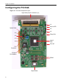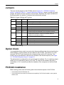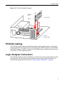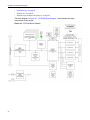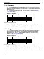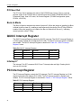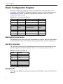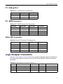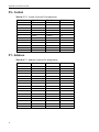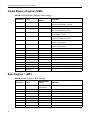
1
PCI334A Quad Serial Communications Controller
PCI334A
Universal I/O 32-bit PCI Quad
Serial Communications Controller
Hardware Manual
Performance Technologies
205 Indigo Creek Drive
Rochester, NY 14626 USA
585.256.0248
[email protected]
www.pt.com
© 2009 Performance Technologies, Inc.
All Rights Reserved.
Document Revision History
Part Number
Date
Explanation of changes
126P0439.10
09/13/03
Initial release
126P0439.11
11/08/04
Updated K7, K8 Switch locations and definitions and new board diagram
126P0439.12
05/24/06
Reformatted
126P0439.20
11/02/09
Reformatted, reorganized, updated cable and RoHS part numbers
Disclaimer
This document presents information for users of Performance Technologies Inc. products.
Although the information contained within this document is considered accurate and
characteristic of the subject product, Performance Technologies Inc. reserves the right to make
changes to this document and any products described herein to improve reliability, functionality,
or design. Performance Technologies Inc. does not assume any liability arising out of the
application or use of any product or circuit described herein. No part of this document may be
copied or reproduced in any form or by any means without the prior permission of Performance
Technologies Inc.
Copyright Notice
© Copyright 2009 by Performance Technologies, Inc. All Rights Reserved.
The Performance Technologies logo is a registered trademark of Performance Technologies,
Inc. All other product and brand names may be trademarks or registered trademarks of their
respective owners.
This document is the sole property of Performance Technologies Inc.
Errors and Omissions
Although diligent efforts are made to supply accurate technical information to the user,
occasionally errors and omissions occur in manuals of this type. Refer to the Performance
Technologies, Inc. Web site to obtain manual revisions or current customer information:
http://www.pt.com.
Performance Technologies, Inc., reserves its right to change product specifications without
notice.
Symbols and Conventions in this Manual
The following symbols appear in this document:
Caution:
There is risk of equipment damage. Follow the instructions.
Warning:
Hazardous voltages are present. To reduce the risk of electrical shock and danger to
personal health, follow the instructions.
2
Contents
Chapter 1: About This Guide
11
Overview . . . . . . . . . . . . . . . . . . . . . . . . . . . . . . . . . . . . . . . . . . . . . . . . . . . . . . . . . . . . . . . . . . . . 11
Text Conventions . . . . . . . . . . . . . . . . . . . . . . . . . . . . . . . . . . . . . . . . . . . . . . . . . . . . . . . . . . . . . 12
Customer Support and Services . . . . . . . . . . . . . . . . . . . . . . . . . . . . . . . . . . . . . . . . . . . . . . . . . . 12
Customer Support Packages . . . . . . . . . . . . . . . . . . . . . . . . . . . . . . . . . . . . . . . . . . . . . . . . . 13
Other Web Support . . . . . . . . . . . . . . . . . . . . . . . . . . . . . . . . . . . . . . . . . . . . . . . . . . . . . . . . . 13
Return Merchandise Authorization (RMA) . . . . . . . . . . . . . . . . . . . . . . . . . . . . . . . . . . . . . . . 13
Product Warranty . . . . . . . . . . . . . . . . . . . . . . . . . . . . . . . . . . . . . . . . . . . . . . . . . . . . . . . . . . . . . 13
Chapter 2: Introduction
15
Overview . . . . . . . . . . . . . . . . . . . . . . . . . . . . . . . . . . . . . . . . . . . . . . . . . . . . . . . . . . . . . . . . . . . . 15
PCI334A Models and Accessories . . . . . . . . . . . . . . . . . . . . . . . . . . . . . . . . . . . . . . . . . . . . . . . . 16
Product Summary . . . . . . . . . . . . . . . . . . . . . . . . . . . . . . . . . . . . . . . . . . . . . . . . . . . . . . . . . . . . . 17
Programming Differences . . . . . . . . . . . . . . . . . . . . . . . . . . . . . . . . . . . . . . . . . . . . . . . . . . . . . . . 18
PCI334A Features . . . . . . . . . . . . . . . . . . . . . . . . . . . . . . . . . . . . . . . . . . . . . . . . . . . . . . . . . . . . 19
MC68360 QUICC . . . . . . . . . . . . . . . . . . . . . . . . . . . . . . . . . . . . . . . . . . . . . . . . . . . . . . . . . . 19
PCI9056 PCI Interface . . . . . . . . . . . . . . . . . . . . . . . . . . . . . . . . . . . . . . . . . . . . . . . . . . . . . . 20
Serial Ports . . . . . . . . . . . . . . . . . . . . . . . . . . . . . . . . . . . . . . . . . . . . . . . . . . . . . . . . . . . . . . . 20
Other Features . . . . . . . . . . . . . . . . . . . . . . . . . . . . . . . . . . . . . . . . . . . . . . . . . . . . . . . . . . . . 20
Required Additional Documents . . . . . . . . . . . . . . . . . . . . . . . . . . . . . . . . . . . . . . . . . . . . . . . . . . 20
Glossary . . . . . . . . . . . . . . . . . . . . . . . . . . . . . . . . . . . . . . . . . . . . . . . . . . . . . . . . . . . . . . . . . . . . 21
Chapter 3: Installation
23
Overview . . . . . . . . . . . . . . . . . . . . . . . . . . . . . . . . . . . . . . . . . . . . . . . . . . . . . . . . . . . . . . . . . . . . 23
Configuring the PCI334A . . . . . . . . . . . . . . . . . . . . . . . . . . . . . . . . . . . . . . . . . . . . . . . . . . . . . . . 24
1
Contents
Jumpers . . . . . . . . . . . . . . . . . . . . . . . . . . . . . . . . . . . . . . . . . . . . . . . . . . . . . . . . . . . . . . . . . . . . 25
Option Clock . . . . . . . . . . . . . . . . . . . . . . . . . . . . . . . . . . . . . . . . . . . . . . . . . . . . . . . . . . . . . . . . . 25
PCI334A Installation . . . . . . . . . . . . . . . . . . . . . . . . . . . . . . . . . . . . . . . . . . . . . . . . . . . . . . . . . . . 25
Installing the PCI334A card into PC . . . . . . . . . . . . . . . . . . . . . . . . . . . . . . . . . . . . . . . . . . . . 26
PCI334A Cabling . . . . . . . . . . . . . . . . . . . . . . . . . . . . . . . . . . . . . . . . . . . . . . . . . . . . . . . . . . . . . 27
Logic Analyzer Connectors . . . . . . . . . . . . . . . . . . . . . . . . . . . . . . . . . . . . . . . . . . . . . . . . . . . . . . 27
Chapter 4: Functional Description
29
Overview . . . . . . . . . . . . . . . . . . . . . . . . . . . . . . . . . . . . . . . . . . . . . . . . . . . . . . . . . . . . . . . . . . . . 29
Power Considerations . . . . . . . . . . . . . . . . . . . . . . . . . . . . . . . . . . . . . . . . . . . . . . . . . . . . . . . . . . 31
MC68360 Quad Integrated Communications Controller . . . . . . . . . . . . . . . . . . . . . . . . . . . . . . . . 31
QUICC Setup . . . . . . . . . . . . . . . . . . . . . . . . . . . . . . . . . . . . . . . . . . . . . . . . . . . . . . . . . . . . . 31
Resets . . . . . . . . . . . . . . . . . . . . . . . . . . . . . . . . . . . . . . . . . . . . . . . . . . . . . . . . . . . . . . . . . . . . . . 35
Optional BDM Port . . . . . . . . . . . . . . . . . . . . . . . . . . . . . . . . . . . . . . . . . . . . . . . . . . . . . . . . . . . . 35
PCI Interface . . . . . . . . . . . . . . . . . . . . . . . . . . . . . . . . . . . . . . . . . . . . . . . . . . . . . . . . . . . . . . . . . 35
Endian Conversion . . . . . . . . . . . . . . . . . . . . . . . . . . . . . . . . . . . . . . . . . . . . . . . . . . . . . . . . . 36
PCI9056 Setup . . . . . . . . . . . . . . . . . . . . . . . . . . . . . . . . . . . . . . . . . . . . . . . . . . . . . . . . . . . . 36
Modes of Operation . . . . . . . . . . . . . . . . . . . . . . . . . . . . . . . . . . . . . . . . . . . . . . . . . . . . . . . . 39
Local bus Arbitration Priority . . . . . . . . . . . . . . . . . . . . . . . . . . . . . . . . . . . . . . . . . . . . . . . . . . 40
PCI9056 Interrupt Requests . . . . . . . . . . . . . . . . . . . . . . . . . . . . . . . . . . . . . . . . . . . . . . . . . . 40
SRAM Array . . . . . . . . . . . . . . . . . . . . . . . . . . . . . . . . . . . . . . . . . . . . . . . . . . . . . . . . . . . . . . . . . 41
Timing . . . . . . . . . . . . . . . . . . . . . . . . . . . . . . . . . . . . . . . . . . . . . . . . . . . . . . . . . . . . . . . . . . . 41
Parity . . . . . . . . . . . . . . . . . . . . . . . . . . . . . . . . . . . . . . . . . . . . . . . . . . . . . . . . . . . . . . . . . . . . 41
Flash PROM . . . . . . . . . . . . . . . . . . . . . . . . . . . . . . . . . . . . . . . . . . . . . . . . . . . . . . . . . . . . . . . . . 41
Line Drivers/Receivers . . . . . . . . . . . . . . . . . . . . . . . . . . . . . . . . . . . . . . . . . . . . . . . . . . . . . . . . . 41
RS232C . . . . . . . . . . . . . . . . . . . . . . . . . . . . . . . . . . . . . . . . . . . . . . . . . . . . . . . . . . . . . . . . . 41
RS422 (EIA530 or RS449 cabling) . . . . . . . . . . . . . . . . . . . . . . . . . . . . . . . . . . . . . . . . . . . . . 42
V.35 . . . . . . . . . . . . . . . . . . . . . . . . . . . . . . . . . . . . . . . . . . . . . . . . . . . . . . . . . . . . . . . . . . . . . 42
Clock Steering . . . . . . . . . . . . . . . . . . . . . . . . . . . . . . . . . . . . . . . . . . . . . . . . . . . . . . . . . . . . . . . . 42
Debug Port . . . . . . . . . . . . . . . . . . . . . . . . . . . . . . . . . . . . . . . . . . . . . . . . . . . . . . . . . . . . . . . . . . 42
Optional Logic Analyzer Connections . . . . . . . . . . . . . . . . . . . . . . . . . . . . . . . . . . . . . . . . . . . . . . 43
Chapter 5: Registers
45
Overview . . . . . . . . . . . . . . . . . . . . . . . . . . . . . . . . . . . . . . . . . . . . . . . . . . . . . . . . . . . . . . . . . . . . 45
TCSL Register . . . . . . . . . . . . . . . . . . . . . . . . . . . . . . . . . . . . . . . . . . . . . . . . . . . . . . . . . . . . . . . 46
Transmit Clock Select . . . . . . . . . . . . . . . . . . . . . . . . . . . . . . . . . . . . . . . . . . . . . . . . . . . . . . . 46
RCSL Register . . . . . . . . . . . . . . . . . . . . . . . . . . . . . . . . . . . . . . . . . . . . . . . . . . . . . . . . . . . . . . . 46
2
Contents
Receive Clock Select . . . . . . . . . . . . . . . . . . . . . . . . . . . . . . . . . . . . . . . . . . . . . . . . . . . . . . . 46
Status Register . . . . . . . . . . . . . . . . . . . . . . . . . . . . . . . . . . . . . . . . . . . . . . . . . . . . . . . . . . . . . . . 47
Presence Detect . . . . . . . . . . . . . . . . . . . . . . . . . . . . . . . . . . . . . . . . . . . . . . . . . . . . . . . . . . . 47
PCI User Out . . . . . . . . . . . . . . . . . . . . . . . . . . . . . . . . . . . . . . . . . . . . . . . . . . . . . . . . . . . . . . 48
Burn-In Mode . . . . . . . . . . . . . . . . . . . . . . . . . . . . . . . . . . . . . . . . . . . . . . . . . . . . . . . . . . . . . 48
QUICC Interrupt Register . . . . . . . . . . . . . . . . . . . . . . . . . . . . . . . . . . . . . . . . . . . . . . . . . . . . . . . 48
Interrupt 7 . . . . . . . . . . . . . . . . . . . . . . . . . . . . . . . . . . . . . . . . . . . . . . . . . . . . . . . . . . . . . . . . 48
PCI Interrupt Register . . . . . . . . . . . . . . . . . . . . . . . . . . . . . . . . . . . . . . . . . . . . . . . . . . . . . . . . . . 48
PCI Interrupt . . . . . . . . . . . . . . . . . . . . . . . . . . . . . . . . . . . . . . . . . . . . . . . . . . . . . . . . . . . . . . 49
Misc. Register . . . . . . . . . . . . . . . . . . . . . . . . . . . . . . . . . . . . . . . . . . . . . . . . . . . . . . . . . . . . . . . . 49
PCI User In . . . . . . . . . . . . . . . . . . . . . . . . . . . . . . . . . . . . . . . . . . . . . . . . . . . . . . . . . . . . . . . 49
LED Disable . . . . . . . . . . . . . . . . . . . . . . . . . . . . . . . . . . . . . . . . . . . . . . . . . . . . . . . . . . . . . . 49
Board Configuration Register . . . . . . . . . . . . . . . . . . . . . . . . . . . . . . . . . . . . . . . . . . . . . . . . . . . . 50
Mechanical Form Factor . . . . . . . . . . . . . . . . . . . . . . . . . . . . . . . . . . . . . . . . . . . . . . . . . . . . . 50
Electrical Interface . . . . . . . . . . . . . . . . . . . . . . . . . . . . . . . . . . . . . . . . . . . . . . . . . . . . . . . . . 50
Revision ID . . . . . . . . . . . . . . . . . . . . . . . . . . . . . . . . . . . . . . . . . . . . . . . . . . . . . . . . . . . . . . . 50
PROM Write Enable Register . . . . . . . . . . . . . . . . . . . . . . . . . . . . . . . . . . . . . . . . . . . . . . . . . . . . 51
PROM Write Enable . . . . . . . . . . . . . . . . . . . . . . . . . . . . . . . . . . . . . . . . . . . . . . . . . . . . . . . . 51
Software ID . . . . . . . . . . . . . . . . . . . . . . . . . . . . . . . . . . . . . . . . . . . . . . . . . . . . . . . . . . . . . . . 51
Chapter 6: QUICC I/O Ports
53
Overview . . . . . . . . . . . . . . . . . . . . . . . . . . . . . . . . . . . . . . . . . . . . . . . . . . . . . . . . . . . . . . . . . . . . 53
QUICC Port A . . . . . . . . . . . . . . . . . . . . . . . . . . . . . . . . . . . . . . . . . . . . . . . . . . . . . . . . . . . . . . . . 54
QUICC Port B . . . . . . . . . . . . . . . . . . . . . . . . . . . . . . . . . . . . . . . . . . . . . . . . . . . . . . . . . . . . . . . . 55
QUICC Port C . . . . . . . . . . . . . . . . . . . . . . . . . . . . . . . . . . . . . . . . . . . . . . . . . . . . . . . . . . . . . . . . 56
Chapter 7: Connector and Cabling
57
Overview . . . . . . . . . . . . . . . . . . . . . . . . . . . . . . . . . . . . . . . . . . . . . . . . . . . . . . . . . . . . . . . . . . . . 57
RS232C Cabling . . . . . . . . . . . . . . . . . . . . . . . . . . . . . . . . . . . . . . . . . . . . . . . . . . . . . . . . . . . . . . 58
RS449 Cabling . . . . . . . . . . . . . . . . . . . . . . . . . . . . . . . . . . . . . . . . . . . . . . . . . . . . . . . . . . . . . . . 60
EIA530 Cabling . . . . . . . . . . . . . . . . . . . . . . . . . . . . . . . . . . . . . . . . . . . . . . . . . . . . . . . . . . . . . . . 63
V.35 Cabling . . . . . . . . . . . . . . . . . . . . . . . . . . . . . . . . . . . . . . . . . . . . . . . . . . . . . . . . . . . . . . . . . 66
Appendix A: Connector Pinouts
69
Overview . . . . . . . . . . . . . . . . . . . . . . . . . . . . . . . . . . . . . . . . . . . . . . . . . . . . . . . . . . . . . . . . . . . . 69
Factory-Installed Connectors . . . . . . . . . . . . . . . . . . . . . . . . . . . . . . . . . . . . . . . . . . . . . . . . . . . . 70
P4 - PCI Connector . . . . . . . . . . . . . . . . . . . . . . . . . . . . . . . . . . . . . . . . . . . . . . . . . . . . . . . . . 70
3
Contents
J1 - 80-pin Connector . . . . . . . . . . . . . . . . . . . . . . . . . . . . . . . . . . . . . . . . . . . . . . . . . . . . . . . 72
P1 - Debug Port . . . . . . . . . . . . . . . . . . . . . . . . . . . . . . . . . . . . . . . . . . . . . . . . . . . . . . . . . . . 73
P2 - BDM Connector . . . . . . . . . . . . . . . . . . . . . . . . . . . . . . . . . . . . . . . . . . . . . . . . . . . . . . . . 73
Altera ISP Connector . . . . . . . . . . . . . . . . . . . . . . . . . . . . . . . . . . . . . . . . . . . . . . . . . . . . . . . 73
Logic Analyzer Connectors . . . . . . . . . . . . . . . . . . . . . . . . . . . . . . . . . . . . . . . . . . . . . . . . . . . . . . 73
P5 - Control . . . . . . . . . . . . . . . . . . . . . . . . . . . . . . . . . . . . . . . . . . . . . . . . . . . . . . . . . . . . . . . 74
P7 - Address . . . . . . . . . . . . . . . . . . . . . . . . . . . . . . . . . . . . . . . . . . . . . . . . . . . . . . . . . . . . . . 74
P6 - Data . . . . . . . . . . . . . . . . . . . . . . . . . . . . . . . . . . . . . . . . . . . . . . . . . . . . . . . . . . . . . . . . . 75
P8 - Clock . . . . . . . . . . . . . . . . . . . . . . . . . . . . . . . . . . . . . . . . . . . . . . . . . . . . . . . . . . . . . . . . 75
Appendix B: Register Value Changes for SRAM
77
Overview . . . . . . . . . . . . . . . . . . . . . . . . . . . . . . . . . . . . . . . . . . . . . . . . . . . . . . . . . . . . . . . . . . . . 77
Global Memory Register (GMR) . . . . . . . . . . . . . . . . . . . . . . . . . . . . . . . . . . . . . . . . . . . . . . . 78
Base Register 1 (BR1) . . . . . . . . . . . . . . . . . . . . . . . . . . . . . . . . . . . . . . . . . . . . . . . . . . . . . . 78
Option Register 1 (OR1) . . . . . . . . . . . . . . . . . . . . . . . . . . . . . . . . . . . . . . . . . . . . . . . . . . . . . 79
Base Register 2 (BR2) . . . . . . . . . . . . . . . . . . . . . . . . . . . . . . . . . . . . . . . . . . . . . . . . . . . . . . 79
Option Register 2 (OR2) . . . . . . . . . . . . . . . . . . . . . . . . . . . . . . . . . . . . . . . . . . . . . . . . . . . . . 80
Appendix C: Agency Approvals
81
Overview . . . . . . . . . . . . . . . . . . . . . . . . . . . . . . . . . . . . . . . . . . . . . . . . . . . . . . . . . . . . . . . . . . . . 81
CE Certification . . . . . . . . . . . . . . . . . . . . . . . . . . . . . . . . . . . . . . . . . . . . . . . . . . . . . . . . . . . . . . . 82
Shielded Cable Notice . . . . . . . . . . . . . . . . . . . . . . . . . . . . . . . . . . . . . . . . . . . . . . . . . . . . . . . . . 82
FCC (USA) Class A Notice . . . . . . . . . . . . . . . . . . . . . . . . . . . . . . . . . . . . . . . . . . . . . . . . . . . . . . 82
Industry Canada Class A Notice . . . . . . . . . . . . . . . . . . . . . . . . . . . . . . . . . . . . . . . . . . . . . . . . . . 83
Safety Information . . . . . . . . . . . . . . . . . . . . . . . . . . . . . . . . . . . . . . . . . . . . . . . . . . . . . . . . . . . . . 83
Safety Precautions . . . . . . . . . . . . . . . . . . . . . . . . . . . . . . . . . . . . . . . . . . . . . . . . . . . . . . . . . 83
Compliance with RoHS and WEEE Directives . . . . . . . . . . . . . . . . . . . . . . . . . . . . . . . . . . . . . . . 84
Index
4
85
Ta b l e s
Table 2-1: PCI334A Part Numbers . . . . . . . . . . . . . . . . . . . . . . . . . . . . . . . . . . . . . . . . . . . . . . . . . . . 16
Table 2-2: PCI334A to PCI334 Product Comparison . . . . . . . . . . . . . . . . . . . . . . . . . . . . . . . . . . . . . 17
Table 3-1: Jumper Settings and Functions . . . . . . . . . . . . . . . . . . . . . . . . . . . . . . . . . . . . . . . . . . . . . 25
Table 4-1: PCI334A Power Consumption in a +5V or Mixed +3.3V / +5V System . . . . . . . . . . . . . . . 31
Table 4-2: Device Address Map . . . . . . . . . . . . . . . . . . . . . . . . . . . . . . . . . . . . . . . . . . . . . . . . . . . . . 32
Table 4-3: QUICC Register Addresses . . . . . . . . . . . . . . . . . . . . . . . . . . . . . . . . . . . . . . . . . . . . . . . . 33
Table 4-4: QUICC Access Timing . . . . . . . . . . . . . . . . . . . . . . . . . . . . . . . . . . . . . . . . . . . . . . . . . . . . 34
Table 4-5: QUICC Interrupt Source Map . . . . . . . . . . . . . . . . . . . . . . . . . . . . . . . . . . . . . . . . . . . . . . . 34
Table 4-6: Addressing for Endian Conversion . . . . . . . . . . . . . . . . . . . . . . . . . . . . . . . . . . . . . . . . . . . 36
Table 4-7: PCI9056 PCI Configuration Register Addresses . . . . . . . . . . . . . . . . . . . . . . . . . . . . . . . . 37
Table 4-8: PCI9056 Local Configuration Register Addresses . . . . . . . . . . . . . . . . . . . . . . . . . . . . . . . 37
Table 4-9: PCI9056 Shared Run Time Register Addresses . . . . . . . . . . . . . . . . . . . . . . . . . . . . . . . . 38
Table 4-10: PCI9056 Local DMA Register Addresses. . . . . . . . . . . . . . . . . . . . . . . . . . . . . . . . . . . . . 38
Table 4-11: PCI Interrupt Register Programming Details . . . . . . . . . . . . . . . . . . . . . . . . . . . . . . . . . . 40
Table 5-1: TCSL Register . . . . . . . . . . . . . . . . . . . . . . . . . . . . . . . . . . . . . . . . . . . . . . . . . . . . . . . . . . 46
Table 5-2: RCSL Register . . . . . . . . . . . . . . . . . . . . . . . . . . . . . . . . . . . . . . . . . . . . . . . . . . . . . . . . . . 46
Table 5-3: Status Register . . . . . . . . . . . . . . . . . . . . . . . . . . . . . . . . . . . . . . . . . . . . . . . . . . . . . . . . . . 47
Table 5-4: SIMM Speeds . . . . . . . . . . . . . . . . . . . . . . . . . . . . . . . . . . . . . . . . . . . . . . . . . . . . . . . . . . . 47
Table 5-5: SIMM Size . . . . . . . . . . . . . . . . . . . . . . . . . . . . . . . . . . . . . . . . . . . . . . . . . . . . . . . . . . . . . 47
5
Tables
Table 5-6: QUICC Interrupt Register . . . . . . . . . . . . . . . . . . . . . . . . . . . . . . . . . . . . . . . . . . . . . . . . . . 48
Table 5-7: PCI Interrupt Register. . . . . . . . . . . . . . . . . . . . . . . . . . . . . . . . . . . . . . . . . . . . . . . . . . . . . 48
Table 5-8: Misc. Register. . . . . . . . . . . . . . . . . . . . . . . . . . . . . . . . . . . . . . . . . . . . . . . . . . . . . . . . . . . 49
Table 5-9: Board Configuration Register . . . . . . . . . . . . . . . . . . . . . . . . . . . . . . . . . . . . . . . . . . . . . . . 50
Table 5-10: Electrical Interface ID . . . . . . . . . . . . . . . . . . . . . . . . . . . . . . . . . . . . . . . . . . . . . . . . . . . . 50
Table 5-11: PROM Write Enable Register. . . . . . . . . . . . . . . . . . . . . . . . . . . . . . . . . . . . . . . . . . . . . . 51
Table 6-1: Port A Configuration Settings . . . . . . . . . . . . . . . . . . . . . . . . . . . . . . . . . . . . . . . . . . . . . . . 54
Table 6-2: QUICC Port A Mapping (16-bit) . . . . . . . . . . . . . . . . . . . . . . . . . . . . . . . . . . . . . . . . . . . . . 54
Table 6-3: Port B Configuration Settings . . . . . . . . . . . . . . . . . . . . . . . . . . . . . . . . . . . . . . . . . . . . . . . 55
Table 6-4: QUICC Port B Mapping (18-bit) . . . . . . . . . . . . . . . . . . . . . . . . . . . . . . . . . . . . . . . . . . . . . 55
Table 6-5: Port C Configuration Settings . . . . . . . . . . . . . . . . . . . . . . . . . . . . . . . . . . . . . . . . . . . . . . . 56
Table 6-6: QUICC Port C Pin Mapping (12-bit) . . . . . . . . . . . . . . . . . . . . . . . . . . . . . . . . . . . . . . . . . . 56
Table 7-1: RS232C Connector Pin Assignments. . . . . . . . . . . . . . . . . . . . . . . . . . . . . . . . . . . . . . . . . 58
Table 7-2: RS449 Connector Pin Assignments . . . . . . . . . . . . . . . . . . . . . . . . . . . . . . . . . . . . . . . . . . 60
Table 7-3: EIA530 Connector Pin Assignments . . . . . . . . . . . . . . . . . . . . . . . . . . . . . . . . . . . . . . . . . 63
Table 7-4: V.35 Connector Pin Assignments. . . . . . . . . . . . . . . . . . . . . . . . . . . . . . . . . . . . . . . . . . . . 66
Table A-1: P4 - PCI Connector Pin Assignments . . . . . . . . . . . . . . . . . . . . . . . . . . . . . . . . . . . . . . . . 70
Table A-2: J1 - High Density 80-pin Connector Pin Assignments . . . . . . . . . . . . . . . . . . . . . . . . . . . . 72
Table A-3: P1 - Debug Port Pin Assignments . . . . . . . . . . . . . . . . . . . . . . . . . . . . . . . . . . . . . . . . . . . 73
Table A-4: P2 - BDM Connector Pin Assignments . . . . . . . . . . . . . . . . . . . . . . . . . . . . . . . . . . . . . . . 73
Table A-5: Altera ISP Connector Pin Assignments . . . . . . . . . . . . . . . . . . . . . . . . . . . . . . . . . . . . . . . 73
Table A-6: Logic Analyzer Connectors Summary . . . . . . . . . . . . . . . . . . . . . . . . . . . . . . . . . . . . . . . . 73
Table A-7: P5 - Control Connector Pin Assignments. . . . . . . . . . . . . . . . . . . . . . . . . . . . . . . . . . . . . . 74
Table A-8: P7 - Address Connector Pin Assignments . . . . . . . . . . . . . . . . . . . . . . . . . . . . . . . . . . . . . 74
Table A-9: P6 - Data Connector Pin Assignments. . . . . . . . . . . . . . . . . . . . . . . . . . . . . . . . . . . . . . . . 75
Table A-10: P8 - Clock Connector Pin Assignments . . . . . . . . . . . . . . . . . . . . . . . . . . . . . . . . . . . . . . 75
Table B-1: SRAM Registers. . . . . . . . . . . . . . . . . . . . . . . . . . . . . . . . . . . . . . . . . . . . . . . . . . . . . . . . . 77
6
Tables
Table B-2: Global Memory Register (GMR) Settings. . . . . . . . . . . . . . . . . . . . . . . . . . . . . . . . . . . . . . 78
Table B-3: Base Register 1 (BR1) Settings . . . . . . . . . . . . . . . . . . . . . . . . . . . . . . . . . . . . . . . . . . . . . 78
Table B-4: Option Register 1 (OR1) Settings . . . . . . . . . . . . . . . . . . . . . . . . . . . . . . . . . . . . . . . . . . . 79
Table B-5: Base Register 2 (BR2) Settings . . . . . . . . . . . . . . . . . . . . . . . . . . . . . . . . . . . . . . . . . . . . . 79
Table B-6: Option Register 2 (OR2) Settings . . . . . . . . . . . . . . . . . . . . . . . . . . . . . . . . . . . . . . . . . . . 80
7
Tables
8
Figures
Figure 2-1: PCI334A Side View Photograph . . . . . . . . . . . . . . . . . . . . . . . . . . . . . . . . . . . . . . . . . . . 18
Figure 3-1: PCI334A Component Layout. . . . . . . . . . . . . . . . . . . . . . . . . . . . . . . . . . . . . . . . . . . . . . 24
Figure 3-2: PCI334A Installation Diagram . . . . . . . . . . . . . . . . . . . . . . . . . . . . . . . . . . . . . . . . . . . . . 27
Figure 4-1: PCI334A Block Diagram . . . . . . . . . . . . . . . . . . . . . . . . . . . . . . . . . . . . . . . . . . . . . . . . . 30
9
Figures
10
Chapter
1
About This Guide
Overview
This manual describes the operation and use of the PCI334A Universal I/O 32-bit Quad Serial
Communications Controller (referred to as the PCI334A in this manual).
In these chapters you will find installation and configuration information, plus a functional block
description intended for the application developer of this board. Here is a brief description of
what you will find in this manual:
Chapter 1, “About This Guide,” this chapter, provides links to all other chapters in this manual,
customer support and services, and product warranty information for the PCI334A.
Chapter 2, “Introduction,” on page 15 describes the PCI334A and the differences between the
PCI334 and the PCI334A.
Chapter 3, “Installation,” on page 23 explains how to configure the PCI334A’s jumpers and
install the PCI334A into the PCI slot in a PC.
Chapter 4, “Functional Description,” on page 29 details power considerations in multi-voltage
environments, QUICC Controller information, and Line drivers and receivers.
Chapter 5, “Registers,” on page 45 describes various PCI334A registers including transmit and
receive clock registers, status registers, and PCI interrupt registers.
Chapter 6, “QUICC I/O Ports,” on page 53 explains the registers, addresses and values for the
QUICC I/O ports A, B, and C.
Chapter 7, “Connector and Cabling,” on page 57 provides the pinouts, signal names and
description for the RS232C, RS449, EIA530 (RS530), and V.35 cables.
11
Chapter 1: About This Guide
Appendix A, “Connector Pinouts,” on page 69 contains tables that describe the pin numbers
and signal names of PCI connectors, Debug port, BDM connector, ISP connector, and optional
logic analyzer connections.
Appendix B, “Register Value Changes for SRAM,” on page 77 contains tables that describe
Global Memory Register (GMR) Settings, Base Register 1 (BR1) Settings, Optional Register 1
(OR1) Settings, Base Register 2 (BR2) Settings, and Option Register 2 (OR2) Settings.
Appendix C, “Agency Approvals,” on page 81 presents agency approval and certification
information.
An “Index,” on page 85, is also provided.
Text Conventions
This guide uses the following conventions:
Convention
What it is Used For
Monospace font
Monospace font is used to represent sample code.
Bold font
Bold font is used to represent:
• pathnames
• filenames
• UNIX commands
• user input
Italic font
Italic font is used to represent:
• notes that supply useful advice
• general information
• referenced documents
Regular font
Regular font is used for the ENTER and TAB keys and the SPACEBAR on your
keyboard.
Customer Support and Services
Performance Technologies offers a variety of standard and custom support packages to ensure
customers have access to the critical resources that they need to protect and maximize
hardware and software investments throughout the development, integration, and deployment
phases of the product life cycle.
If you encounter difficulty in using this Performance Technologies, Inc. product, you may
contact our support personnel by:
1. EMAIL (Preferred Method) – Email us at the addresses listed below or use our online email support
form. Outline your problem in detail. Please include your return email address and a telephone
number.
2. TELEPHONE – Contact us via telephone at the number listed below, and request Technical Support.
Our offices are open Monday to Friday, 8:00 a.m. to 8:00 p.m. (Eastern Standard Time).
If you are located outside North America, we encourage you to contact the local Performance
Technologies’ distributor or agent for support. Many of our distributors or agents maintain
technical support staffs.
12
Product Warranty
Performance Technologies Support Contact Information
Embedded Systems and Software
(Includes Platforms, Blades, and Servers)
SS7 Systems
(Includes SEGway™)
Email
[email protected]
[email protected]
Phone
+1 (585) 256-0248
(Monday to Friday, 8 a.m. to 8 p.m.
Eastern Standard Time)
+1 (585) 256-0248
(Monday to Friday, 8 a.m. to 8 p.m.
Eastern Standard Time)
Customer Support Packages
Our configurable development and integration support packages help customers maximize
engineering efforts and achieve time-to-market goals. To find out more about our Customer
Support packages, visit http://www.pt.com/page/support/.
Other Web Support
Support for existing products including manuals, release notes, and drivers can be found on
specific product pages at http://www.pt.com. Use the product search to locate the information
you need.
Return Merchandise Authorization (RMA)
To submit a return merchandise authorization (RMA) request, complete the online RMA form
available at http://pt.com/assets/lib/files/rma-request-form.doc and follow the instructions on
the form. You will be notified with an RMA number once your return request is approved.
Shipping information for returning the unit to Performance Technologies will be provided once
the RMA is issued.
Product Warranty
Performance Technologies, Incorporated, warrants that its products sold hereunder will at the
time of shipment be free from defects in material and workmanship and will conform to
Performance Technologies’ applicable specifications or, if appropriate, to Buyer’s specifications
accepted by Performance Technologies in writing. If products sold hereunder are not as
warranted, Performance Technologies shall, at its option, refund the purchase price, repair, or
replace the product provided proof of purchase and written notice of nonconformance are
received by Performance Technologies within 12 months of shipment, or in the case of
software and integrated circuits within ninety (90) days of shipment and provided said
nonconforming products are returned F.O.B. to Performance Technologies’s facility no later
than thirty days after the warranty period expires. Products returned under warranty claims
must be accompanied by an approved Return Material Authorization number issued by
Performance Technologies and a statement of the reason for the return. Please contact
Performance Technologies, or its agent, with the product serial number to obtain an RMA
number. If Performance Technologies determines that the products are not defective, Buyer
shall pay Performance Technologies all costs of handling and transportation. This warranty
shall not apply to any products Performance Technologies determines to have been subject to
testing for other than specified electrical characteristics or to operating and/or environmental
conditions in excess of the maximum values established in applicable specifications, or have
13
Chapter 1: About This Guide
been subject to mishandling, misuse, static discharge, neglect, improper testing, repair,
alteration, parts removal, damage, assembly or processing that alters the physical or electrical
properties. This warranty excludes all cost of shipping, customs clearance and related charges
outside the United States. Products containing batteries are warranted as above excluding
batteries.
THIS WARRANTY IS IN LIEU OF ALL OTHER WARRANTIES WHETHER EXPRESS,
IMPLIED OR STATUTORY INCLUDING IMPLIED WARRANTIES OF MERCHANTABILITY OR
FITNESS. IN NO EVENT SHALL PERFORMANCE TECHNOLOGIES BE LIABLE FOR ANY
INCIDENTAL OR CONSEQUENTIAL DAMAGES DUE TO BREACH OF THIS WARRANTY
OR ANY OTHER OBLIGATION UNDER THIS ORDER OR CONTRACT.
14
Chapter
2
Introduction
Overview
This document provides information for users of the PCI334A Universal I/O 32-bit PCI Quad
Serial Communications Controller.
Note: Performance Technologies, Inc. has a similar product with a very similar model name,
the PCI344. Ensure that you are using the correct manual for the applicable product.
This manual is not intended as a stand-alone document. If you plan on writing software for this
product the references cited in the “Required Additional Documents,” on page 20 are
necessary to have a complete understanding of all the features and functions of the hardware.
This manual does provide the information necessary to understand the operation and features
of the board. A prime objective was to answer those questions raised by system developers as
to whether the PCI334A will complement their architecture. When combined with the required
documentation listed below, a complete description of PCI334A facilities are presented.
Topics covered in this chapter include:
•
“PCI334A Models and Accessories,” on page 16
•
“Product Summary,” on page 17
•
“Programming Differences,” on page 18
•
“PCI334A Features,” on page 19
•
“Required Additional Documents,” on page 20
•
“Glossary,” on page 21
15
Chapter 2: Introduction
PCI334A Models and Accessories
Table 2-1, “PCI334A Part Numbers,” lists the PTI part numbers for the models and accessories
available for the PCI334A.
Table 2-1: PCI334A Part Numbers
Item
Non-RoHS Part Number
RoHS Part Number
Four Port Sync. Serial Controller (RS232C)
PT-PCI334A-11666
PT-PCI334A-11890
Four Port Sync. Serial Controller (RS449/EIA530)
PT-PCI334A-11667
PT-PCI334A-11891
Four Port Sync. Serial Controller (V.35)
PT-PCI334A-11668
PT-PCI334A-11892
Four Port V.35 Hydra Cable, DTE with thumbscrews
PT-ACC334-10622
PT-ACC334-11918
Four Port RS232C Hydra Cable, DTE with jackscrews
PT-ACC334-10623
PT-ACC334-11919
Four Port RS232C Hydra Cable, DTE with thumbscrews
-
PT-ACC334-12274
Four Port EIA530 Hydra Cable, DTE with jackscrews
PT-ACC334-10624
PT-ACC334-11969
Four Port EIA530 Hydra Cable, DTE with thumbscrews
-
PT-ACC334-12273
Four Port RS449 Hydra Cable, (Socket) Sun Substitute, DTE with
jackscrews
PT-ACC334-10741
PT-ACC334-11920
Four Port RS449 Hydra Cable, (Pin) DTE with jackscrews
PT-ACC334-10722
PT-ACC334-11921
PCI334A Versions
Cable Options
RoHS/Non-RoHS Notice
This manual covers both RoHS and Non-RoHS versions of the PCI334A. It is important to
know what version of the PCI334A you are using to obtain accurate information for set-up,
installation and the proper use of the product. See “Compliance with RoHS and WEEE
Directives,” on page 84 for more information.
16
Product Summary
Product Summary
The PCI334A PCI Quad Communications Controller (shown in Figure 2-1, “PCI334A Side View
Photograph,” on page 18) is a design update to the PCI334A, required due to components
obsolescence. As part of this update, certain characteristics of the PCI334A are revised or
enhanced. Maintaining software compatibility at the user level is the prime objective. Table 2-2,
“PCI334A to PCI334 Product Comparison,” summarizes the differences between the old and
new designs.
Table 2-2: PCI334A to PCI334 Product Comparison
Feature
PCI334 (Old)
PCI334A (New)
Power Supply
5V, +/-12V required for operation
Can be run in 5V or mixed 3.3V / 5V
backplane with on-board switching
power supply. All components are 3.3V.
VIO
5V only
3.3V or 5V (Universal I/O signaling))
PCI Interface
PLX PCI9060, 5V
PLX PCI9056, 3.3V
PCI Speed
33 MHz only
66 MHz (33MHz jumper selectable)
Processor
68360 rev L, 5V
68360 rev L, 3.3V
Memory
4 Megabyte 60 ns DRAM SIMM,
expandable to 16 Megabyte
4 Megabytes 70 ns SRAM, fixed size,
factory installed
Boot Flash
AM29F010, 128K x 8, 5V
AM29LV040, 512 K x 8, 3.3V
Hardware Reset
QUICC generated
Hardware generated
RS232C Data Rate
40 Kbps maximum
(14C88/14C89, 5V, +/-12V)
250 Kbps minimum
(ICL3223E, 3.3V)
RS422
26LS31/26LS32, 5V
MAX3031E/MAX3096, 3.3V
V.35
LTC1345, 5V
LTC2846/ICL3223E, 3.3V
Optional Oscillator
Surface mount solderable location for
plastic part, 5V
Socket for half-size can shielded
oscillator, 3.3V1
Console Connector
Straight
Right angle
Programmable Logic
Fixed
In circuit programmable
Board revision ID
External resistors
Internal to PLD
PCI Device ID
0x0334
0x334a
Software ID
---
6
PCI Bracket
Mounted from bottom side
Mounted from top side
Chassis to Digital
Ground Connection
Zero ohm resistors
Jumper
1. Socket not present on the RoHS version.
17
Chapter 2: Introduction
Figure 2-1: PCI334A Side View Photograph
Programming Differences
Some modifications are necessary to the QUICC register values for proper operation of the
PCI334A with the SRAM instead of the DRAM SIMM on the PCI334. These disable the DRAM
controller and enable the SRAM controller. The registers are:
•
Global Memory Register
•
Base Register 1
•
Option Register 1
•
Base Register 2
•
Option Register 2
Further description of the changes can be found in Appendix B, “Register Value Changes for
SRAM,” on page 77.
In addition, the PCI Device ID has been changed to 0x334a. This is in one of the PCI9056
Configuration Registers. A new register field has been added, the Software ID. It is in the
PROM Write Enable Register (one of the local registers). Its value is 6 (decimal).
18
PCI334A Features
PCI334A Features
MC68360 QUICC
•
•
•
•
•
•
•
•
CPU32+ Processor (4.5 MIPS at 25 MHz)
•
32-Bit Version of the CPU32 Core (Fully Compatible with the CPU32)
•
Background Debug Mode
•
Byte-Misaligned Addressing
Four General Purpose Timers
•
Superset of MC68302 Timers
•
Four 16-Bit Timers or Two 32-Bit Timers
Two Independent DMAs (IDMAs)
•
Single Address Mode for Fastest Transfers
•
Buffer Chaining and Auto Buffer Modes
•
Automatically Performs Efficient Packing
System Integration Module (SIM60)
•
Bus Monitor
•
Double Bus Fault Monitor
•
Software Watchdog
•
Periodic Interrupt Timer
•
Low Power Stop Mode
•
Breakpoint Logic Provides On-Chip Hardware Breakpoints
Four Serial Communication Controllers (SCC)
•
HDLC/SDLC™
•
Signaling System #7 (SS7)
•
Binary Synchronous Communication (BISYNC)
•
Totally Transparent (Bit Streams)
•
Totally Transparent (Frame Based with Optional Cyclic Redundancy Check (CRC))
•
Asynchronous HDLC
•
DDCMP™
•
V.14
•
X.21
Two Serial Management Controllers (SMC)
•
UART
•
Transparent
•
General Circuit Interface (GCI) Controller
Communications Processor Module (CPM)
•
RISC Controller
•
224 Buffer Descriptors
•
Supports Continuous Mode Transmission and Reception on All Serial Channels
•
2.5 KBytes of Dual-Port RAM
•
14 Serial DMA Channels
Four Baud Rate Generators
19
Chapter 2: Introduction
•
Independent (can be connected to any SCC or SMC)
•
Allows Changes During Operation
•
Autobaud Support Option
PCI9056 PCI Interface
•
PCI Compliance Revision 2.2
•
32-bit, 66 MHz operation
•
Register compatible with PCI9054, PCI9656, PCI9060, and PCI9080
•
PCI Bus Master Transfers up to 264 MBps
•
Two Independent DMA Channels
•
Bi-Directional Chaining DMA Controller
•
Two Bi-Directional FIFOs for DMA
•
Four FIFOs for Direct Master/Slave Read/Write
•
Eight 32-bit Mailboxes and Two 32-bit Doorbell Registers
Serial Ports
•
Full RS232C, RS422, or V.35 Support on All Four Ports
•
Optional On-Board Clock Provision
•
Internal or External Serial Data Clocks
•
Five Modem Control Signals per Port (Seven for V.35 configuration)
Other Features
•
4 MByte 70 ns Dual Ported Low Power Asynchronous Static RAM
•
512 KByte (4Mbit) Flash PROM (boot)
•
On-board RS232 Debug Port
•
Mechanical - ISA/EISA Short Length, 3.3V/5V, 32-bit PCI Card
Required Additional Documents
PCI Local Bus Specification
Revision 2.2, 1998. PCI Special Interest Group; 2575 N.E. Kathryn #17, Hillsboro, OR 97214.
More information at: http://www.pcisig.com/
MC68360 QUICC User’s Manual Rev 1
MC68360UM/AD; Motorola Incorporated. Motorola Literature Distribution; P.O. Box 20912;
Phoenix, AZ 85036.
Available at: http://www.motorola.com/semiconductors/
PLX PCI9056 Databook
Product Catalog. PLX Technology, 870 Maude Avenue; Sunnyvale, CA 94085.
More information at: http://www.plxtech.com/
20
Glossary
Glossary
Bps
Bytes per second
bps
Bits per second
CPU
Central Processing Unit
DMA
Direct Memory Access, hardware controller block data transfers
DMAC
Direct Memory Access Controller
DRAM
Dynamic Random Access Memory
half-word
In this manual, this term indicates a 16-bit value
HDLC
High-Level Data Link Control
Lbus
Local PCI334A on-board bus
MByte
Megabyte
MPU
Micro-Processor Unit
ms.
Millisecond
PCI9056
PCI Bus Master Interface Chip
QUICC
Quad Integrated Communications Controller
reserved
The term used for bits, bytes, fields, code values, etc. that are set
aside for future use
SCC
QUICC Serial Communications Controller
SDLC
Synchronous Data Link Control
SMC
QUICC Serial Management Controllers
word
In this manual, this term indicates a 32-bit value
xxh
Numbers followed by lowercase h are hexadecimal values. All other
numbers are decimal values To help with readability, large
hexadecimal values use a ‘.’ to indicate 16 bit (4 nibble) boundaries. In
this document, the period does not indicate a decimal place in a
hexadecimal number
21
Chapter 2: Introduction
22
Chapter
3
Installation
Overview
This chapter describes how to configure the PCI334A’s jumpers and install the PCI334A into
the PCI slot in a PC.
Topics covered in this chapter include:
•
“Configuring the PCI334A,” on page 24
•
“Jumpers,” on page 25
•
“Option Clock,” on page 25
•
“PCI334A Installation,” on page 25
•
“PCI334A Cabling,” on page 27
•
“Logic Analyzer Connectors,” on page 27
Installation is a three step process:
•
Configure the PCI334A for your application.
•
Install the PCI334A.
•
Bring up your system.
23
Chapter 3: Installation
Configuring the PCI334A
Figure 3-1: PCI334A Component Layout
High Density 80-pin Connector (J1)
K1
Burn-in LED
Option Clock
K2
K3
K5
Debug Port
K6
K7
QUICC
Chip
K8
PLD ISP
PCI
Connector
PCI9056
PCI Interface
SRAM
Flash PROM
24
Jumpers
Jumpers
There are several jumpers on the PCI334A, shown in Figure 3-1, “PCI334A Component
Layout,” on page 24. Table 3-1, “Jumper Settings and Functions,” shows a summary of board
jumpers. No special tools are required to move jumpers. Reposition the jumpers as defined in
the following table. An asterisk (*) indicates the normal factory settings.
Table 3-1: Jumper Settings and Functions
Jumper
Pins
In/Out
Function
K1
1-2
In
Connect Digital to Chassis ground
2-3
In*
Isolate Digital from Chassis ground
1-2
In*
Normal mode
K2
2-3
In
Burn-In mode
K3
1-2
Out*
Manually forces Hardware Reset to the QUICC
K5
1-2
In*
PCI9056 initially RETRY PCI configuration accesses
2-3
In
PCI9056 initially NOT RESPOND to PCI configuration accesses
1-2
In*
M66EN signal input from backplane. When high, it configures for
operation above 33 MHz to a maximum of 66 MHz. When low,
operation is from 25 MHz to 33 MHz.
2-3
In
M66EN signal is grounded, forcing operation from 25 MHz to 33 MHz.
1-2
In*
Normal mode
2-3
In
Delay GNT# signal one PCI clock
1-2
In*
Normal mode
2-3
In
Delay GNT# signal one PCI clock
K6
K7
K8
* Factory Default Setting
Option Clock
If your application has a need for a receive clock frequency different than that received from the
serial interface, a crystal oscillator can be installed on the PCI334A. The location U17 is silkscreened “OPTCLK” and is located on the component side near the PCI connector. This
location can be populated with a half size can oscillator of the desired frequency. See Figure
3-1, “PCI334A Component Layout,” on page 24.
The optional clock is configured for a four-pin through hole oscillator. Pin 1 is a pulled-up output
enable, pin 4 is connected to ground, pin 5 is the TTL output of the oscillator, and pin 8 is
connected to +3.3V. A socket is provided for installation of the component on the Non-RoHS
version.
PCI334A Installation
Before starting, please note the following about the mechanical aspects of the PCI334A:
•
The PCI334A meets PCI Revision 2.2.
•
The PCI334A has been tested for mechanical compatibility. The PCI334A installs in most systems
without issue.
25
Chapter 3: Installation
Installing the PCI334A card into PC
Use the following steps to install the PCI334A card into a PCI slot. See Figure 3-2, “PCI334A
Installation Diagram,” on page 27.
Caution:
Electronic components on printed circuit boards are extremely sensitive to static electricity.
Ordinary amounts of static electricity generated by your clothing or work environment can
damage the electronic equipment. It is recommended that when installing the PCI334A in a
system that anti-static grounding straps and anti-static mats are used to help prevent
damage due to electrostatic discharge.
1. Quit all applications. Power down the PC and any attached peripherals. Remove the top cover of the
PC.
2. Configure the PCI334A. See “Configuring the PCI334A,” on page 24 for a complete description of
setup issues and jumper configuration procedures.
3. Select an available PCI slot and remove the slot filler panel.
4. Slide the PCI334A into the PCI connector of the system unit. Make sure the front plate on the
PCI334A card mounts flush with the chassis panel opening.
5. Install the front plate screw to secure the PCI334A card into the chassis. This also provides a chassis
ground connection to the PCI334A.
6. Replace the top cover.
7. Install the serial port cable assembly to the PCI334A connector.
8. Reconnect any cables from the peripheral devices. This completes the hardware installation. At this
point, turn power back on to the PC and proceed to any Software Installation Instructions that may
have been provided.
26
PCI334A Cabling
Figure 3-2: PCI334A Installation Diagram
PCI334A Cabling
The PCI334A provides external connectivity through a passive cabling system. A hydra-style
connector provides front panel serial port connectivity to four DB25 connectors for the RS232C
and EIA530 versions, four DB37 connectors for the RS449 version, and M34 connectors for the
V.35 version, in DTE configuration (pins).
Logic Analyzer Connectors
The PCI334A permits the optional installation of connectors for use by a logic analyzer or other
test equipment. The connectors must be installed on the secondary side of the board. The
connector pin assignments can be found in “Logic Analyzer Connectors,” on page 73.
27
Chapter 3: Installation
28
Chapter
4
Functional Description
Overview
The PCI334A Universal I/O 32-bit Quad Serial Communications Controller provides four serial
channel interfaces for high performance synchronous communications on a PCI host system.
The design incorporates a Motorola MC68360 Quad Integrated Communications Controller
(QUICC) and a PLX PCI9056 with DMA capability. Code storage and data buffering are
provided by an SRAM array, which is shared between the QUICC and the PCI9056.
Serial line electrical interfacing is available on-board providing voltage level adaptation to a
Recommended Standard, such as RS232C, RS422 (RS449 or EIA530 cabling), or V.35.
The PCI bracket interface connection on the PCI334A uses an 80-pin Amplimite receptacle
containing the signals for all four ports. To provide an industry standard connection for each
port, hydra-style adapter cables are offered. Adapter cable wiring details for each style cable is
also provided.
The PCI334A supports an optional crystal oscillator to provide custom synchronous clock
speeds. A single green LED is provided as a software-controlled indicator.
Topics covered in this chapter include:
•
“Power Considerations,” on page 31
•
“MC68360 Quad Integrated Communications Controller,” on page 31
•
“Resets,” on page 35
•
“Optional BDM Port,” on page 35
•
“PCI Interface,” on page 35
•
“SRAM Array,” on page 41
•
“Flash PROM,” on page 41
•
“Line Drivers/Receivers,” on page 41
29
Chapter 4: Functional Description
•
“Clock Steering,” on page 42
•
“Debug Port,” on page 42
•
“Optional Logic Analyzer Connections,” on page 43
The block diagram in Figure 4-1, “PCI334A Block Diagram,” demonstrates the major
components of this design.
Figure 4-1: PCI334A Block Diagram
30
Power Considerations
Power Considerations
The PCI334A is a Universal I/O card, meaning it is compatible with either +3.3V or +5V VIO on
the PCI backplane. The PLX PCI9056 interface chip can tolerate these voltages.
The board is designed to operate in +5V only and mixed +5V/+3.3V powered backplanes.
Typical and maximum power consumption of the PCI334A is presented in Table 4-1, “PCI334A
Power Consumption in a +5V or Mixed +3.3V / +5V System,” on page 31. +12V and –12V are
not used by the PCI334A.
Table 4-1: PCI334A Power Consumption in a +5V or Mixed +3.3V / +5V System
Board Type
Voltage
Typical
Maximum
PCI334A-11890 (RS232C)
+3.3V
0A
0A
PCI334A-11890 (RS232C)
+5V
0.7A
0.9A
PCI334A-11891 (RS422)
+3.3V
0A
0A
PCI334A-11891 (RS422)
+5V
0.7A
0.9A
PCI334A-11892 (V.35)
+3.3V
0A
0A
PCI334A-11892 (V.35)
+5V
1.1A
1.4A
MC68360 Quad Integrated Communications
Controller
The PCI334A incorporates a Motorola MC68360 Quad Integrated Communications Controller
(QUICC).
QUICC Setup
The QUICC requires concentrated effort in the set up of its configuration register set. The
MC68360 Quad Integrated Communications Controller, User’s Manual is the best source for
information into the details of programming and operation of the QUICC.
Device Address Map
The PCI334A internal address space is divided into eight major areas using the GeneralPurpose Chip-Select feature of the QUICC. The decoding, provided by the Chip Select logic, is
controlled by the Global Memory Register (GMR) and the Memory Controller Status Register
(MSTAT). See the QUICC User’s Manual for more information on the GMR and MSTAT
registers.
The address map of each functional element is provided in Table 4-2, “Device Address Map,”
on page 32. The QUICC occupies 8 KBytes of address space for internal memory and
registers. The base address for these is stored in the Memory Base Address Register (MBAR)
which resides at the fixed address of 0003.FF00h. Since the MBAR is programmable, the
beginning addresses for the internal Dual-Ported RAM (DPRBASE) and the internal registers
(REGB) are relocatable.
31
Chapter 4: Functional Description
This map applies for QUICC and PCI slave accesses. A single PROM device contains the
QUICC Boot Firmware as well as the PCI configuration information. The QUICC has access to
the entire address range as shown in this table. The PCI Bus has access to the entire range
with the exception of the local boot PROM.
PCI slave accesses to the Local bus arbitrate for Local bus with the QUICC chip. When the
PCI9056 is master of the Local bus, the address and control signals are enabled and the
QUICC’s System Integration Module (SIM60) provides address decoding for the various
resources. The function code is generated by logic, and is fixed at the value of 05h
(Supervisory Data space).
Table 4-2: Device Address Map
1.
2.
3.
4.
32
Device
Size1
Data
Width2
QUICC
Address
PCI
Address3
Purpose
Pin
PROM
512 KB
Byte
0000.0000h
NA
Boot Firmware
CS0
QUICC
1W
Word
0003.FF00h
0003.FF00h
MBAR
QUICC
4 KB
varies
0004.0000h
0004.0000h
DPRBASE
QUICC
4 KB
varies
0004.1000h
0004.1000h
REGB
PCI9056
Registers
256 B
Word
0010.0000h
CFG/Host4
PCI9056 Registers
CS7
Status Register
1B
Word
0010.1000h
0010.1000h
Board Status
CS6
QUICC
Interrupt
Register
1b
Word
0010.1100h
0010.1100h
QUICC L7 Interrupt
CS6
PCI Interrupt
Register
1b
Word
0010.1200h
0010.1200h
PCI Interrupt
CS6
Misc. Register
1B
Word
0010.1300h
0010.1300h
Misc. PCI9056 Control
CS6
Reserved
1B
Word
0010.1400h
0010.1400h
Reserved
CS6
Reserved
1B
Word
0010.1500h
0010.1500h
Reserved
CS6
Board Config
Register
1B
Word
0010.1600h
0010.1600h
Misc. Configuration
Info
CS6
PROM WE
Register
1b
Word
0010.1700h
0010.1700h
PROM Write Enable
CS6
TCSL Register
1B
Word
0011.0200h
0011.0200h
Transmit Clock Select
CS5
RCSL Register
1B
Word
0011.0300h
0011.0300h
Receive Clock Select
CS5
SRAM
2 MB
variable
0040.0000h
0040.0000h
Code/Data
CS1
SRAM
2 MB
variable
0060.0000h
0060.0000h
Code/Data
CS2
Reserved
CS3
Reserved
CS4
B=Byte, b=bit
Word=32 bits
PCI Address indicates offset from PCI Base Address Local Address Space 0 value loaded by the host.
PCI Address for PCI9056 Registers (Local Config, Shared Run Time) indicates offset from PCI Base
Address for Mapped Runtime Registers value loaded by the host. PCI9056 PCI Config Registers ()
are accessed by PCI Configuration (CFG) cycles.
MC68360 Quad Integrated Communications Controller
QUICC Register Setup
All internal memory and registers of the QUICC occupy a single 8-KByte memory block that is
relocatable along 8-KByte boundaries. The location is fixed by writing the desired base address
of the 8-KByte memory block to the Memory Base Address Register (MBAR). The MBAR
resides at a fixed location in 0003.FF00. The MBAR is a write only register.
The 8-KByte block is divided into two 4-KByte sections. The dual port RAM occupies the first
section; the internal registers occupy the second section. The starting addresses of these two
sections are referred to in the QUICC manual as the Dual-Port RAM Base (DPRBASE) and the
Register Base (REGB), respectively.
The MBAR is loaded at initialization time with a value of 0004.0000. This determines the values
of DPRBASE and REGB. Note that these are not actually registers but base addresses. Table
4-3, “QUICC Register Addresses,” is a list of the critical QUICC registers and settings for
proper board operation.
Table 4-3: QUICC Register Addresses
Register
QUICC Address
Width in Bits
Setting
MBAR
0003.FF00h1
32
0x00040000
DPRBASE
0004.0000h2
32
NA
REGB
0004.1000h3
32
NA
MCR
0004.1000h
32
0x0000ec7f
AVR
0004.1008h
8
0xa0
CLKOCR
0004.100Ch
8
0x0c
PLLCR
0004.1010h
16
0x8000
CDVCR
0004.1014h
16
0x0780
PEPAR
0004.1016h
16
0x0440
SYPCR
0004.1022h
8
0x0c
GMR
0004.1040h
32
0x000000004
BR0
0004.1050h
32
0x00000001
OR0
0004.1054h
32
0x3ff80004
BR1
0004.1060h
32
0x004000094
OR1
0004.1064h
32
0x2fe000004
BR2
0004.1070h
32
0x006000094
OR2
0004.1074h
32
0x2fe000004
BR3
0004.1080h
32
0xf00000014
OR3
0004.1084h
32
0xf00000064
BR4
0004.1090h
32
0xd00000014
OR4
0004.1094h
32
0x3ff8000404
BR5
0004.10a0h
32
0x00110001
OR5
0004.10a4h
32
0x4ffff800
BR6
0004.10b0h
32
0x00101001
OR6
0004.10b4h
32
0x4ffff800
BR7
0004.10c0h
32
0x00100001
OR7
0004.10c4h
32
0xfffff8064
33
Chapter 4: Functional Description
1.
2.
3.
4.
MBAR is at a fixed address. The value in MBAR determines the value of DPRBASE and REGB
Base Address of QUICC Dual-Port RAM section.
Base Address of QUICC Register section
revised from PCI334
The base and option register settings correspond to the device address map provided in Table
4-2, “Device Address Map,” on page 32, and the device access timing provided for reference in
Table 4-4, “QUICC Access Timing,” on page 34.
The QUICC I/O ports are explained Chapter 6, “QUICC I/O Ports,” on page 53.
Table 4-4: QUICC Access Timing
Device Type
Device Speed
Tcyc1
Memory Cycle Time2
# Wait States
PROM
90 ns.
3
200 ns.
2
SRAM
70 ns.
1
120 ns.
1
Registers
15 ns.
8
400 ns.
7
PCI Master
N.A.
-
1. Tcyc = Value loaded into memory controller’s option register for the internally generated DSACKs
N.A. means Not Applicable because the DSACK signals are generated by logic external to the 68360.
2. 68360 Address Strobe period plus one clock cycle.
QUICC Interrupts
The QUICC receives an interrupt at level 7 from the QUICC Interrupt Register accessible by
the PCI Bus at the address defined in Table 4-2, “Device Address Map,” on page 32. This
interrupt is asserted by setting the MSb (D31). The interrupt is removed when this bit is cleared
(write D31 = 0). The value of this latch may be read at any time. This interrupt is defined on the
QUICC as auto-vectored and its state may be verified by reading the D31 bit. This register
contains a Flip-Flop that maintains the state of the interrupt request. This interrupt is also
cleared when reset is asserted, removing any pending requests. The QUICC Interrupt Register
is described in full in Chapter 5, “Registers,” on page 45.
A QUICC level 7 interrupt may also be generated from a software watchdog option available on
the QUICC. This option is controlled in the QUICC SYPCR.
The QUICC receives an interrupt at level 5 from several sources via the PCI9056. This interrupt
can be cleared by disabling the source’s enable bit, or clearing the cause of the interrupt. See
"PCI Interrupt" on page 49 for more information.
Table 4-5, “QUICC Interrupt Source Map,” defines interrupts to the QUICC and the process by
which they are removed.
Table 4-5: QUICC Interrupt Source Map
Source
Level
Vector1
Removal Service
PCI9056 Local Interrupt
5
Auto-vectored
Clear source or remove enable
QUICC Interrupt Register
7
Auto-vectored
Clear MSB in register
7
Auto-vectored
Acknowledge Cycle
Software Watchdog
Option2
1. Those auto-vectored interrupts must be programmed as such by means of the MC68360 IP’s Auto Vector Register.
2. The software watchdog timer (SWT) can be programmed to generate a board Reset or a level 7 interrupt with programmable vector number.
34
Resets
Timers
The QUICC has four general purpose timer modules, a periodic interrupt timer, a software
watchdog timer, and a bus cycle period monitor.
The software watchdog timer may be used to interrupt the CPU, or reset the PCI334A logic and
CPU. This QUICC reset output does not initialize the PCI9056.
Bus cycles performed by the CPU are monitored by a timer within the QUICC. This is controlled
by the BME bit and the BMT field of the SYPCR (register).
Resets
The PCI Reset signal has the effect of initializing all of the PCI334A logic. This signal is
normally asserted during a power up PCI reset by the Host system. The PCI Reset is
distributed to the QUICC Soft Reset (RESETS) pin and other on-board logic.
The QUICC may generate a Soft RESET by execution of the RESET instruction, or a watchdog
time-out. This initializes the QUICC and its control logic and resets the Local Bus portion of the
PCI9056, re-initializing all local configuration registers.
The QUICC can also be reset by asserting the signal on the Hard RESET pin. This pin is
attached to the optional background debug mode connector. Asserting this signal initializes the
QUICC and its control logic and resets the Local Bus portion of the PCI9056, re-initializing all
local configuration registers.
A host may also hold the PCI334A in reset by setting the PCI Adapter Software Reset bit in the
PCI9056 “EEPROM Control, PCI Command Codes, User I/O Control, Init Control Register.”
Setting this bit generates a continuous Soft Reset.
Optional BDM Port
The PCI334A permits the addition of a 2 x 5-pin header strip in position P2 so that a
Background Debug Mode (BDM) Connector may be added (Samtec1, part number TSM-15-01S-DV). P2 allows a thru-hole header on the component side of the board. P2 is defined in the
QUICC manual Section 9.9 (page 9-94). A momentary reset switch may be attached to the
RESETH pin (P2 PIN 7) to provide a convenience during development. The pinout for the BDM
port is shown in Table A-4, “P2 - BDM Connector Pin Assignments,” on page 73.
PCI Interface
The PCI9056 requires concentrated effort in the setup of its configuration and runtime
registers. The PCI9056 data sheet is the best source for information into the details of
programming and operating the PCI9056.
See Figure 3-1, “PCI334A Component Layout,” on page 24.
1. Samtec’s Web site is http://www.samtec.com/.
35
Chapter 4: Functional Description
Endian Conversion
Proper care must be taken when accessing local addresses from the PCI Bus and PCI9056
Registers from the local bus. The hardware does not handle endian conversion from the big
endian local bus to the little endian PCI Bus (and interface). Accesses from the PCI Bus less
than 32-bits wide must change the lower two address bits for proper data bytes to be read/
written as shown in Table 4-6, “Addressing for Endian Conversion,” on page 36.
The QUICC has the capability to transmit and receive SCC data using little endian byte
ordering instead of the standard big endian byte ordering. This is set up in the QUICC’s RFCR
and TFCR registers.
Table 4-6: Addressing for Endian Conversion
Data
Local Address Offset
PCI Address Offset
D31-D24 (byte)
00b
11b
D23-D16 (byte)
01b
10b
D15-D8 (byte)
10b
01b
D7-D0 (byte)
11b
00b
D31-D16 (half-word)
00b
10b
D15-D0 (half-word)
10b
00b
D31-D0 (word)
00b
00b
PCI9056 Setup
PCI9056 registers can be accessed by either the QUICC or the PCI Host (except DMA
registers, which can only be accessed by the QUICC). The PCI9056 Configuration Register
Select signal (CCS#, driven by +S0) is set to properly decode accesses to internal PCI9056
registers. The allocated register space for the PCI9056 registers is shown in Table 4-2, “Device
Address Map,” on page 32. When initialization of PCI9056 registers is complete, the user
should set the Local Init Status bit in the PCI9056 “EEPROM Control (not supported on the
PCI334A), PCI Command Codes, User I/O Control, Init Control Register.” Until this bit is set,
the PCI334A will issue retries to all PCI accesses.
PCI Registers
The PCI registers must be programmed locally from the PROM device, since the serial
EEPROM option of the PCI9056 is not used. Until the Local Init Done bit in the PCI9056 Init
Control Register is set, indicating the configuration registers have been loaded, PCI cycles will
be terminated with retries by the PCI9056. Both Configuration Read (type 0 or 1) and
Configuration Write (type 0 or 1) PCI cycles are supported.
Doorbell Registers
There are two 32-bit doorbell interrupt/status registers in the PCI9056. One is assigned to the
PCI bus interface, while the other is assigned to the Local bus interface. Doorbell registers are
used to pass interrupts between the PCI bus and Local bus.
36
PCI Interface
Mailbox Registers
There are eight 32-bit mailbox registers in the PCI9056. These registers are used to pass
command and status information between the PCI Host and the QUICC.
Table 4-7: PCI9056 PCI Configuration Register Addresses
Register
Local Address
Width in Bits
Setting
Device ID
0010.0000h
16
0x334a
Vendor ID
0010.0002h
16
0x1214
Status
0010.0004h
16
0x0280
Command
0010.0006h
16
0x0107
Class Code
0010.0008h
24
0x068000
Revision ID
0010.000bh
8
0x10
BIST
0010.000ch
8
0x00
Header Type
0010.000dh
8
0x00
Latency Timer
0010.000eh
8
0x42
Cache Line Size
0010.000fh
8
0x00
PCI BA Mem Mapped Reg
0010.0010h
32
Host
PCI BA I/O Mapped Reg
0010.0014h
32
Host
PCI BA Local AddrSpace 0
0010.0018h
32
Host
PCI BA Local Exp ROM
0010.0030h
32
Host
Max_lat
0010.003ch
8
0x00
Min Gnt
0010.003dh
8
0x00
Interrupt Pin
0010.003eh
8
0x01
Table 4-8: PCI9056 Local Configuration Register Addresses
Register
Local Address
Width in Bits
Setting
PCI-Local Range
0010.0080h
32
0xff800000
PCI-Local Base
0010.0084h
32
0x00000001
PCI-ROM Range
0010.0090h
32
0xffff0000
PCI-ROM Range
0010.0094h
32
0x0
PCI-Local Desc
0010.0098h
32
0x40030003
DM-PCI Range
0010.009ch
32
0x0
DM-PCI Mem BA
0010.00a0h
32
0x0
DM-PCI Cfg LBA
0010.00a4h
32
0x0
DM-PCI PBA
0010.00a8h
32
0x0
DM-PCI Cfg PCA
0010.00ach
32
0x0
37
Chapter 4: Functional Description
Table 4-9: PCI9056 Shared Run Time Register Addresses
Register
Local Address
Width in Bits
Setting
Mailbox Reg 0
0010.00c0h
32
0x0
Mailbox Reg 1
0010.00c4h
32
0x0
Mailbox Reg 2
0010.00c8h
32
0x0
Mailbox Reg 3
0010.00cch
32
0x0
Mailbox Reg 4
0010.00d0h
32
0x0
Mailbox Reg 5
0010.00d4h
32
0x0
Mailbox Reg 6
0010.00d8h
32
0x0
Mailbox Reg 7
0010.00dch
32
0x0
PCI-Loc Doorbell
0010.00e0h
32
0x0
Loc-PCI Doorbell
0010.00e4h
32
0x0
Interrupt Ctrl/Status
0010.00e8h
32
0x00010100
Control1
0010.00ech
32
0x8801767e
Misc.
1. Also known as the “EEPROM Control, PCI Command Codes, User I/O Control, Init Control Register.”
Table 4-10: PCI9056 Local DMA Register Addresses
38
Register
Local Address
Width in Bits
Setting
DMA Ch 0 Mode
0010.0100h
32
0x00000043
DMA0 PCI Addr
0010.0104h
32
0x0
DMA0 Loc Addr
0010.0108h
32
0x0
DMA0 Trans Cnt
0010.010ch
32
0x0
DMA0 Desc Ptr
0010.0110h
32
0x0
DMA Ch 1 Mode
0010.0114h
32
0x00000043
DMA1 PCI Addr
0010.0118h
32
0x0
DMA1 Loc Addr
0010.011ch
32
0x0
DMA1 Trans Cnt
0010.0120h
32
0x0
DMA1 Desc Ptr
0010.0124h
32
0x0
DMA Cmd/Status
0010.0128h
32
0x0
DMA Arb Reg 0
0010.012ch
32
0x0
DMA Arb Reg 1
0010.0130h
32
0x0
PCI Interface
Modes of Operation
Direct Master
The PCI334A does not support direct access to the PCI bus by the QUICC. Only DMA
accesses may be sourced to the PCI bus as discussed below.
Direct Slave
The PCI334A supports both memory mapped (Memory Read, Memory Read Multiple, Memory
Read Line) and I/O mapped (I/O Read) accesses to the Local bus from the PCI bus. The direct
slave interface contains a 128-byte Read FIFO and a 256-byte Write FIFO. PCI base address
registers are provided in the PCI9056 configuration space to set up the adapter’s location in
PCI memory and
I/O space. Byte (8-bit), Half-Word (16-bit), and Word (32-bit) accesses are supported to local
SRAM, local registers, and the QUICC internal registers.
Setup of the PCI9056 Local Configuration Registers (specifically the Local Address Space 0 /
Expansion ROM Bus Region Descriptor) must include enabling the Ready Input and disabling
the Bterm input for Memory Space 0. The Burst Enable bit may be set but offers no advantage.
All sourced burst accesses from the PCI9056 are broken up into non-burst local accesses by
hardware.
DMA Operation
The PCI9056 supports two independent DMA channels capable of transferring data from the
Local bus (SRAM) to the PCI bus. Both chaining and non-chaining DMA transfers are
supported. DMA channels 0 and 1 both contain 256-byte bi-directional FIFOs. DMAs can
generate Memory Read, Memory Write, Memory Read Multiple, and Memory Read Line PCI
cycles. Demand mode DMA is not supported.
The DMA registers inside the PCI9056 are accessible only from the Local bus (QUICC). Setup
of the PCI9056’s Local DMA Registers (specifically the DMA Channel 0 Mode) must include
enabling the Ready Input and disabling the Bterm input for both DMA channels. The Burst
Enable bit may be set but offers no advantage. All sourced burst accesses from the PCI9056
are broken up into non-burst local accesses by hardware.
PCI User In/Out
The PCI9056 contains two user-defined bits. The User Out bit is an output of the PCI9056
which can be read from the Status Register defined in “Misc. Register,” on page 49. The User
In bit is an input to the PCI9056 which can be set in the Misc. Register as described in “Misc.
Register,” on page 49. Both User bits are found in the PCI9056 “EEPROM Control, PCI
Command Codes, User I/ O Control, Init Control Register.”
39
Chapter 4: Functional Description
Local bus Arbitration Priority
QUICC internal masters have highest priority during arbitration requests, followed by PCI
accesses via the PCI9056. The QUICC’s CPU32 core has the lowest priority. The arbitration
between the CPU32 and QUICC internal masters (such as IDMA or SDMA) is handled internal
to the QUICC.
PCI9056 Interrupt Requests
PCI Interrupt Requests
A level A PCI interrupt (INTA#) can be generated from the PCI9056 Local to PCI Doorbell
Register, the PCI Interrupt Register, or a PCI9056 master/target abort status condition. The
level A PCI Interrupt signal or individual sources of the interrupt can be enabled or disabled
through the PCI9056 Interrupt Control/Status Register. This register also provides interrupt
status for each source of the interrupt. The PCI Interrupt can be cleared by disabling a source’s
interrupt enable bit or by clearing the cause of the interrupt.
PCI supports four interrupt levels (A,B,C,D). The level A PCI interrupt is the only PCI interrupt
signal supported by the PCI334A. The PCI Interrupt Pin Register in the PCI9056 configuration
space indicates the PCI interrupt level used and must be programmed to reflect the use of
INTA#.
The PCI Interrupt Register is a programmable latch described in the following table. A PCI
interrupt can be generated when bit 31 of this location is set. The interrupt is removed when
this bit is cleared. The value of this latch may be read at any time. The PCI Interrupt Register is
described in detail in “PCI Interrupt Register,” on page 48.
Table 4-11: PCI Interrupt Register Programming Details
Interrupted Device
Interrupt Request Level
Register
Address
PCI
A
PCI Interrupt Register
0010.1200h
PCI to QUICC Interrupt Requests
The PCI9056 PCI to Local Doorbell Register, a PCI BIST interrupt, or a PCI9056 DMA channel
interrupt can generate a QUICC level 5 interrupt. The PCI9056 local interrupt pin (LINTO#) or
individual sources of the interrupt can be enabled or disabled through the PCI9056 Interrupt
Control/Status Register. This register also provides interrupt status for each source of interrupt.
The interrupt can be cleared by disabling a source’s interrupt enable bit or by clearing the
cause of the interrupt.
40
SRAM Array
SRAM Array
The SRAM array has a 32-bit data width and is implemented using four micro ball grid array
surface mount components. SRAM control is embedded in the QUICC chip and it provides 1
Wait State (2 clocks @ 25MHz) Read and Write cycle period for MC68360 accesses (for 70-ns
SRAM). Memory size is fixed at-4 MB due to factory-installed memory. The presence detect
bits are hard coded in a PLD to represent a 4 MB, 70 ns module for software compatibility. They
may be read from the Status Register as shown in “Status Register,” on page 47.
See Figure 3-1, “PCI334A Component Layout,” on page 24.
Timing
All SRAM control signals and timing are controlled directly from the QUICC. All timing is set up
through the QUICC’s GMR, BRx, and ORx. For SRAM timing information see Table 4-4,
“QUICC Access Timing,” on page 34.
Parity
Parity is not supported on SRAM accesses.
Flash PROM
The Flash PROM device is a 512-KB x 8-bit (4-Mb), AM29LV040-90 32-pin 3.3V PLCC device.
It is socketed on the board. Updating can be performed by setting the PROM_WE bit in the
PROM WE Register as shown in “PROM Write Enable Register,” on page 51 and performing
an erase and reprogramming algorithm per the manufacturer’s specifications.
The Flash PROM is not accessible from the PCI Bus. If programming from the host is desired,
first transfer the data into local SRAM, then locally program the PROM via the QUICC.
See Figure 3-1, “PCI334A Component Layout,” on page 24.
Line Drivers/Receivers
Line drivers and receivers provide electrical adaptation from TTL levels to the appropriate
communications interface signal levels. Currently RS232C, RS422, and V.35 electrical
interfaces are available. Serial ports 1-4 are connected to QUICC SCC1-4, respectively. The
electrical interface supported by a PCI334A can be read from the Board Configuration Register
as shown in “Board Configuration Register,” on page 50.
RS232C
The PCI334A-11890 (RS232C) will service each port with six RS232C inputs and four RS232C
outputs. The RS232C drivers/receivers operate up to 100-Kbits/s and meet TIA/EIA-232-F and
ITU V.28. Cabling is available with male DB25 DTE connectors to provide an RS232C
interface.
41
Chapter 4: Functional Description
RS422 (EIA530 or RS449 cabling)
The PCI334A-11891 (RS422) will service each port with six RS422 inputs and four RS422
outputs. The six inputs for each port are electrically terminated with a resistor network
equivalent to 120 ohms between the designated “A” and “B” circuits of each. The RS422
drivers/receivers operate up to 10-Mbits/s. Cabling is available with male DB37 DTE
connectors or female DB37 DCE connectors to provide an RS449 interface. The EIA530
interface is supported electrically but cabling with male DB25 DTE connectors is not a standard
product.
V.35
The PCI334A-11892 (V.35) will service each port with seven V.35/ Bell 306 inputs and five V.35/
Bell 306 outputs. Four of the seven inputs and three of the five outputs are unbalanced and
electrically compatible with V.28 (RS232C). The remaining three inputs and two outputs are
balanced but somewhat different from V.11 (RS422). The V.35 drivers/ receivers operate up to
10-Mbits/s. Cabling is available with male M34 DTE connectors to provide a V.35 interface
Clock Steering
For synchronous serial applications, transmit and receive data signals may be accompanied by
external transmit and/or receive clock signals. To manage the options for each clock line
source and destination, a clock multiplexor is provided. The source and direction of the clocks
are set up in the TCSL Register and the RCSL Register as shown in “TCSL Register,” on page
46 and “RCSL Register,” on page 46.
The transmit clock of any channel may be sourced from the QUICC’s transmit clock signals
(TXCx) or from the serial port’s transmit clock in signal (TXCIx).
The receive clock of any serial channel can be sourced from the serial port receive clock
signals (RCLKx) or can be sourced from an optional clock (OPTCLK) at location U17. The user
may install a half-size can (through-hole) oscillator module of any desired frequency and
tolerance (3.3V part). For diagnostic mode, the receive clock may be sourced from inside the
QUICC.
Debug Port
A 3-pin header is provided at P1 for the debug port, which is connected to the QUICC’s SMC1
port. The TTL signals of SMC1 are converted to RS232C voltage levels on-board. This
connector is 3-pins 0.025” in diameter, spaced 0.100” apart. Table A-3, “P1 - Debug Port Pin
Assignments,” on page 73 indicates the wiring for a console cable to a DB25 connector for the
debug port. This console cable (part number 11-160Q053310) is available by special order
from Performance Technologies. Please see “Customer Support and Services,” on page 12.
During SMC1 initialization, a break sequence can be enabled to generate an interrupt. If the
debug port is left unconnected to a terminal, the QUICC’s SMC1 port will receive all 0s, thus
generating break sequences. Therefore, do not enable the break sequence interrupt to prevent
unwanted interrupts.
See Figure 3-1, “PCI334A Component Layout,” on page 24.
42
Optional Logic Analyzer Connections
Optional Logic Analyzer Connections
Locations have been provided for the optional user installation of through-hole header strips for
the connection of external test equipment. These are installed on the bottom side of the board.
The pinouts and suggested vendor part numbers for these connectors are shown in Table A-6,
“Logic Analyzer Connectors Summary,” on page 73.
43
Chapter 4: Functional Description
44
Chapter
5
Registers
Overview
Topics covered in this chapter include:
•
“TCSL Register,” on page 46
•
“RCSL Register,” on page 46
•
“Status Register,” on page 47
•
“QUICC Interrupt Register,” on page 48
•
“PCI Interrupt Register,” on page 48
•
“Misc. Register,” on page 49
•
“Board Configuration Register,” on page 50
•
“PROM Write Enable Register,” on page 51
Note: Unused bits in local registers should be written to 0. Unused bits have undefined values
during local register reads.
45
Chapter 5: Registers
TCSL Register
The TCSL (transmit clock select) Register provides the PCI334A with control of the source of
the transmit clocks for each serial port. The TCSL Register is a 32-bit register located at local
address 0011.0200h.
The TCSL Register is readable and writable. The TCSL Register is described in Table 5-1,
“TCSL Register,” below.
Table 5-1: TCSL Register
Bit
Mnemonic
Function
Reset Value
31
TCSL1
Transmit Clock Select 1
0
30
TCSL2
Transmit Clock Select 2
0
29
TCSL3
Transmit Clock Select 3
0
28
TCSL4
Transmit Clock Select 4
0
27-0
-
Unused
-
Transmit Clock Select
The Transmit Clock Select (TCSLx) bit controls the source of the port’s transmit clock. When
set, the transmit clock is sourced from the serial interface. When the bit is cleared, the transmit
clock is sourced from the QUICC’s transmit clock output.
RCSL Register
The RCSL (receive clock select) Register provides the PCI334A with control of the source of
the receive clocks for each serial port. The RCSL Register is a 32-bit register located at
address 0011.0300h. The RCSL Register is readable and writable. The RCSL Register is
described in Table 5-2, “RCSL Register,”below.
Table 5-2: RCSL Register
Bit
Mnemonic
Function
Reset Value
31
RCSL1
Receive Clock Select 1
0
30
RCSL2
Receive Clock Select 2
0
29
RCSL3
Receive Clock Select 3
0
28
RCSL4
Receive Clock Select 4
0
27-0
-
Unused
-
Receive Clock Select
The Receive Clock Select bit controls the source of the port’s receive clock. When set, the
receive clock is sourced from the optional oscillator. When the bit is cleared, the receive clock
is sourced from the serial interface.
46
Status Register
Status Register
The Status Register provides status of on-board signals for monitoring The Status Register is a
read only, 32-bit register located at local address 0010.1000h. The Status Register is described
in Table 5-3, “Status Register,” below.
Table 5-3: Status Register
Bit
Mnemonic
Function
Reset Value
31
PD4
Presence Detect 4
PD4
30
PD3
Presence Detect 3
PD3
29
PD2
Presence Detect 2
PD2
28
PD1
Presence Detect 1
PD1
27
-
Reserved
1
26
USERO
PCI User Out
1
25
MODE
Mode
MODE
24
-
Reserved
0
23-0
-
Unused
-
Presence Detect
On the PCI334A, the Presence Detect (PD) bits are hard coded in a PLD to represent an
uninstalled DRAM SIMM (all PB bits high). Following is some background information
describing the original purpose of these bits.
The Presence Detect bits identify the size and speed of DRAM SIMM installed into the SIMM
socket. The encoding presented on these pins can be read in Speed and Size fields, where
Speed 1, Speed 0, Size 1, and Size 0 correspond to SIMM Presence Detect bits 4, 3, 2, and 1,
respectively.
Note: The encoding of the SIMM presence detect pins can vary from DRAM vendor to vendor.
Table 5-4, “SIMM Speeds,” and Table 5-5, “SIMM Size,” show typical encoding for the SIMM
Presence Detect pins.
Table 5-4: SIMM Speeds
Speed Field
Speed (ns)
0
100
1
80
2
70
3
60
Table 5-5: SIMM Size
Size Field
Size (MB)
0
4
1
2,32
2
1,16
3
8
47
Chapter 5: Registers
PCI User Out
The PCI User Out bit indicates the status of the PCI9056 User Out pin. This is a general
purpose output of the PCI9056 that is controlled from the PCI9056 “EEPROM Control, PCI
Command Codes, User I/O Control, Init Control Register” (PCI9056 configuration space,
PCI6Ch, LOC ECh).
Burn-In Mode
The Burn-In Mode bit indicates the status of jumper K2. When the jumper is installed, the BurnIn Mode bit will be clear (0), enabling a mode reserved for the factory if the PT-Bug PROM is
installed. When the jumper in not installed, the Burn-In Mode bit will be set (1), indicating
normal operation under PT-Bug.
QUICC Interrupt Register
The QUICC Interrupt Register controls the QUICC interrupts. The QUICC Interrupt Register is
a 32-bit register located at local address 0010.1100h. The QUICC Interrupt register is readable
and writable. The QUICC Interrupt Register is described in Table 5-6, “QUICC Interrupt
Register,” below.
Table 5-6: QUICC Interrupt Register
Bit
Mnemonic
Function
Reset Value
31
IR7
QUICC Interrupt Level 7
0
30-24
-
Reserved
0
23-0
-
Unused
-
Interrupt 7
The Interrupt 7 bit (IR7) causes a QUICC level 7 interrupt when set high. Clearing the bit
removes the interrupt.
PCI Interrupt Register
The PCI Interrupt Register controls the PCI interrupts. The PCI Interrupt Register is a 32-bit
register located at local address 0010.1200h. The PCI Interrupt register is readable and
writable. The PCI Interrupt Register is described in Table 5-7, “PCI Interrupt Register,” below.
Table 5-7: PCI Interrupt Register
48
Bit
Mnemonic
Function
Reset Value
31
PINT
PCI Interrupt
0
30-24
-
Reserved
0
23-0
-
Unused
-
Misc. Register
PCI Interrupt
The PCI Interrupt (PINT) bit causes a PCI Interrupt when set. Clearing this bit removes the
interrupt. The PCI Interrupt is mapped to PCI INTA#, INTB#, INTC#, or INTD# through the
PCI9056 PCI Interrupt Pin Register (PCI9056 configuration space, offset 3Dh). Hardware
requires this register must map the PCI Interrupt to INTA#.
Misc. Register
The Misc. Register controls the miscellaneous functions of the PCI334A. The Misc. register is a
32-bit register located at local address 0010.1300h. The Misc. Register is both readable and
writable. The Misc. Register is described in Table 5-8, “Misc. Register,” below.
Table 5-8: Misc. Register
Bit
Mnemonic
Function
Reset Value
31
DREQ1
DMA Channel 1 Request (not supported)
0
30
DREQ0
DMA Channel 0 Request (not supported)
0
29
USERI
PCI User In
0
28
-
Reserved
0
27
LED_DIS
LED Disable
1
26-24
-
Reserved
0
23-0
-
Unused
-
PCI User In
The PCI User In (USERI) bit indicates the status of the PCI9056 User In pin. This is a generalpurpose input of the PCI9056 that is controlled from the PCI9056 “EEPROM Control, PCI
Command Codes, User I/O Control, Init Control Register” (PCI9056 configuration space,
PCI6Ch, LOC ECh).
LED Disable
The LED Disable (LED_DIS) bit is connected to the on-board green LED. When set (1), the
LED will be disabled (off). When the bit is 0, the LED is on.
49
Chapter 5: Registers
Board Configuration Register
The Board Configuration Register is a read only register that includes information on the
configuration of the PCI334A. The Board Configuration register is a 32-bit register located at
local address 0010.1600h. The Board Configuration is described in Table 5-9, “Board
Configuration Register,” below.
Table 5-9: Board Configuration Register
Bit
Mnemonic
Function
Reset Value
31
-
Reserved
0
30
FORM
Mechanical Form Factor
FORM
29
INT2
Electrical Interface 2
INT2
28
INT1
Electrical Interface 1
INT1
27
INT0
Electrical Interface 0
INT0
26
ID2
Revision ID 2
ID2
25
ID1
Revision ID 1
ID1
24
ID0
Revision ID 0
ID0
23-0
-
Unused
-
Mechanical Form Factor
The Mechanical Form Factor of the card is indicated by the Form bit. When set, this indicates
the mechanical form factor is PCI (ISA). A low (0) value of this bit is reserved for future use.
Electrical Interface
The Electrical Interface (INT[2:0]) bits indicate the electrical interface supported by the card.
Available supported interfaces are listed in Table 5-10, “Electrical Interface ID,” below.
Table 5-10: Electrical Interface ID
Int[2:0]
Interface
000
RS232C
001
RS422 (449/530)
010
V.35
011
Reserved
100
Reserved
101
Reserved
110
Reserved
111
None Installed
Revision ID
The Revision ID (ID[2:0]) bits indicate the revision of the PCI334A. A revision ID of 000 is the
lowest ID.
50
PROM Write Enable Register
PROM Write Enable Register
The PROM Write Enable Register contains the protection bit for enabling/disabling writing to
the PROM. This register also contains the Software ID field. The PROM Write Enable Register
is a 32-bit register located at local address 0010.1700h. The PROM Write Enable Register is
readable and writable. The PROM Write Enable Register is described in Table 5-11, “PROM
Write Enable Register,” below.
Table 5-11: PROM Write Enable Register
Bit
Mnemonic
Function
Reset Value
31
PWE
PROM Write Enable
0
30
-
Reserved
0
29-24
SID
Software ID
000110
23-0
-
Unused
-
PROM Write Enable
The PROM Write Enable (PWE) bit, when set, enables programming of the PROM. When
cleared (0), the PROM is a read only device.
Software ID
This is 6 (decimal) for the PCI334A.
51
Chapter 5: Registers
52
Chapter
6
QUICC I/O Ports
Overview
The QUICC has three general-purpose I/O ports A, B and C. Each pin in I/O ports may be
configured as a general-purpose I/O pin or as a dedicated peripheral interface pin. The
PCI334A design uses these ports as described below.
Topics covered in this chapter include:
•
“QUICC Port A,” on page 54
•
“QUICC Port B,” on page 55
•
“QUICC Port C,” on page 56
53
Chapter 6: QUICC I/O Ports
QUICC Port A
Assignment of Port A pins including their direction is accomplished by configuring the PAPAR,
PADIR, and PAODR registers on the QUICC. An example configuration for Port A is shown in
Table 6-1, “Port A Configuration Settings,” below.
Table 6-1: Port A Configuration Settings
QUICC Register
QUICC Address
Value
PAPAR
0004.1552h
0xffff
PADIR
0004.1550h
0x5500
PAODR
0004.1554h
0x0000
PADAT
0004.1556h
Value
The PCI334A uses Port A on the QUICC for serial port transmit and receive clocks and data.
Bit assignments are shown in Table 6-2, “QUICC Port A Mapping (16-bit),” may be configured
as either inputs or outputs. The definition is dependent upon the clock steering settings for
transmit clocks.
The Direction column in Table 6-2 indicates the direction of the signal with respect to the
QUICC.
Table 6-2: QUICC Port A Mapping (16-bit)
54
QUICC pin/cell
Use
Signal
Name
QUICC Name
Direction
PA00
Receive Data Port 1
RXD1
RXD1
I
PA01
Transmit Data Port 1
TXD1
TXD1
O
PA02
Receive Data Port 2
RXD2
RXD2
I
PA03
Transmit Data Port 2
TXD2
TXD2
O
PA04
Receive Data Port 3
RXD3
RXD3
I
PA05
Transmit Data Port 3
TXD3
TXD3
O
PA06
Receive Data Port 4
RXD4
RXD4
I
PA07
Transmit Data Port 4
TXD4
TXD4
O
PA08
Transmit Clock Port 1
TXC1
CLK1/BRG01
I/O
PA09
Receive Clock Port 1
RXC1
CLK2
I
PA10
Transmit Clock Port 2
TXC2
CLK3/BRG02
I/O
PA11
Receive Clock Port 2
RXC2
CLK4
I
PA12
Transmit Clock Port 3
TXC3
CLK5/BRG03
I/O
PA13
Receive Clock Port 3
RXC3
CLK6
I
PA14
Transmit Clock Port 4
TXC4
CLK7/BRG04
I/O
PA15
Receive Clock Port 4
RXC4
CLK8
I
QUICC Port B
QUICC Port B
Assignment of Port B pins including their direction is accomplished by configuring the PBPAR,
PBDIR, and PBODR registers on the QUICC. An example configuration for Port B is shown in
Table 6-3, “Port B Configuration Settings,” below.
Table 6-3: Port B Configuration Settings
QUICC Register
QUICC Address
Value
PBPAR
0004.16bch
0x0000
PBDIR
0004.16b8h
0xf00f
PBODR
0004.16c2h
0x0000
PBDAT
0004.16c4h
Value
The PCI334A uses Port B on the QUICC for modem control signals and the debug port
transmit and receive signals. Bit assignments are shown in Table 6-4, “QUICC Port B Mapping
(18-bit),” on page 55. RTS signals may be configured as a dedicated signal used by the
QUICC’s SCC or as a general purpose output pin. The Direction column in Table 6-4 indicates
the direction of the signal with respect to the QUICC.
Table 6-4: QUICC Port B Mapping (18-bit)
QUICC pin/cell
Use
Signal
Name
QUICC Name
Direction
PB00
Line Test Port 1 (V.35 only)
LT1
PORT B0
O
PB01
Line Test Port 2 (V.35 only)
LT2
PORT B1
O
PB02
Line Test Port 3 (V.35 only)
LT3
PORT B2
O
PB03
Line Test Port 4 (V.35 only)
LT4
PORT B3
O
PB04
Data Set Ready Port 1
DSR1
PORT B4
I
PB05
Data Set Ready Port 2
DSR2
PORT B5
I
PB06
Debug Port Transmit Data
TXD
SMTXD1
I
PB07
Debug Port Receive Data
RXD
SMRXD1
O
PB08
Data Set Ready Port 3
DSR3
PORT B8
I
PB09
Data Set Ready Port 4
DSR4
PORT B9
I
PB10
Ring Indicator Port 1 (V.35 only)
RI1
PORT B10
I
PB11
Ring Indicator Port 2 (V.35 only)
RI2
PORT B11
I
PB12
Request To Send Port 1
RTS1
PORT B12/RTS1
O
PB13
Request To Send Port 2
RTS2
PORT B13/RTS2
O
PB14
Request To Send Port 3
RTS3
PORT B14/RTS3
O
PB15
Request To Send Port 4
RTS4
PORT B15/RTS4
O
PB16
Ring Indicator Port 3 (V.35 only)
RI3
PORT B16
I
PB17
Ring Indicator Port 4 (V.35 only)
RI4
PORT B17
I
55
Chapter 6: QUICC I/O Ports
QUICC Port C
Assignment of Port C pins including their direction is accomplished by configuring the PCPAR,
PCDIR, PCSO, and PCINT registers on the QUICC. An example configuration for Port C is
shown in Table 6-5, “Port C Configuration Settings,” below. Each of the Port C pins may be
programmed individually to cause an interrupt to the QUICC CPU32 core as described in the
MC68360 User’s Manual.
Table 6-5: Port C Configuration Settings
QUICC Register
QUICC Address
Value
PCPAR
0004.1562h
0x0000
PCDIR
0004.1560h
0x000f
PCSO
0004.1564h
0x0000
PCDAT
0004.1566h
Value
PCINT
0004.1568h
0x0000
The PCI334A uses Port C on the QUICC for modem control signals. The assignment of Port C
pins is defined in Table 6-6, “QUICC Port C Pin Mapping (12-bit),” below. CTS and DCD signals
may be configured as dedicated signals used by the QUICC’s SCC or as general-purpose
output pins. The Direction column in Table 6-6 indicates the direction of the signal with respect
to the QUICC.
Table 6-6: QUICC Port C Pin Mapping (12-bit)
56
QUICC pin/cell
Use
Signal
Name
QUICC Name
Direction
PC00
Data Terminal Ready Port 1
DTR1
PORT C0
O
PC01
Data Terminal Ready Port 2
DTR2
PORT C1
O
PC02
Data Terminal Ready Port 3
DTR3
PORT C2
O
PC03
Data Terminal Ready Port 4
DTR4
PORT C3
O
PC04
Clear To Send Port 1
CTS1
PORT C4/CTS1
I
PC05
Data Carrier Detect Port 1
DCD1
PORT C5/CD1
I
PC06
Clear To Send Port 2
CTS2
PORT C6/CTS2
I
PC07
Data Carrier Detect Port 2
DCD2
PORT C7/CD2
I
PC08
Clear To Send Port 3
CTS3
PORT C8/CTS3
I
PC09
Data Carrier Detect Port 3
DCD3
PORT C9/CD3
I
PC10
Clear To Send Port 4
CTS4
PORT C10/ CTS4
I
PC11
Data Carrier Detect Port 4
DCD4
PORT C11/CD4
I
Chapter
7
Connector and Cabling
Overview
All versions of the PCI334A have an 80-pin Amplimite connector providing the signals for all
four serial ports. The pinout of the Amplimite connector is described in the cabling sections
below. See Figure 3-1, “PCI334A Component Layout,” on page 24 for connector location.
Topics covered in this chapter include:
•
“RS232C Cabling,” on page 58
•
“RS449 Cabling,” on page 60
•
“EIA530 Cabling,” on page 63
•
“V.35 Cabling,” on page 66
57
Chapter 7: Connector and Cabling
RS232C Cabling
A shielded, hydra-style breakout cable providing four 25-pin, D-shell (DB25) DTE (pins)
connectors is available for the PCI334A-11890 (RS232C) version. The pin assignments for the
cabling and connectors are shown in Table 7-1, “RS232C Connector Pin Assignments,” below.
Table 7-1: RS232C Connector Pin Assignments
80-Pin
No.
Signal
Name
RS232C
Mnemonic
RS232C DB25
Pin No.
Description
1
RXD1
BB
3
Port 1 Receive Data
2
3
16
DTR1
CD
4
5
TXD1
BA
RTS1
CA
TXC1
DA
TXCI1
DB
DCD1
CF
24
Port 1 Transmit Clock
15
Port 1 Transmit Clock In
8
Port 1 Data Carrier Detect
10
DSR1
CC
16
6
Port 1 Data Set Ready
22
17
CTS1
CB
5
Port 1 Clear To Send
18
GND1
AB
7
Port 1 Signal Ground
19
RXC1
DD
17
Port 1 Receive Clock
20
21
9
RXD2
BB
22
23
25
DTR2
CD
TXD2
BA
RTS2
CA
TXC2
DA
TXCI2
DB
DCD2
CF
4
Port 2 Request To Send
24
Port 2 Transmit Clock
15
Port 2 Transmit Clock In
8
Port 2 Data Carrier Detect
10
DSR2
CC
36
37
Port 2 Transmit Data
12
34
35
2
11
32
33
Port 2 Data Terminal Ready
19
30
31
20
14
28
29
Port 2 Receive Data
23
26
27
3
16
24
58
Port 1 Request To Send
12
14
15
4
11
12
13
Port 1 Transmit Data
19
10
11
2
14
8
9
Port 1 Data Terminal Ready
23
6
7
20
6
Port 2 Data Set Ready
22
CTS2
CB
5
Port 2 Clear To Send
RS232C Cabling
Table 7-1: RS232C Connector Pin Assignments (Continued)
80-Pin
No.
Signal
Name
RS232C
Mnemonic
RS232C DB25
Pin No.
Description
38
GND2
AB
7
Port 2 Signal Ground
39
RXC2
DD
17
Port 2 Receive Clock
40
41
9
RXD3
BB
42
43
DTR3
CD
TXD3
BA
RTS3
CA
TXC3
DA
TXCI3
DB
4
Port 3 Request To Send
24
Port 3 Transmit Clock
15
Port 3 Transmit Clock In
12
DCD3
CF
54
55
Port 3 Transmit Data
11
52
53
2
19
50
51
Port 3 Data Terminal Ready
14
48
49
20
23
46
47
Port 3 Receive Data
16
44
45
3
8
Port 3 Data Carrier Detect
10
DSR3
CC
56
6
Port 3 Data Set Ready
22
57
CTS3
CB
5
Port 3 Clear To Send
58
GND3
AB
7
Port 3 Signal Ground
59
RXC3
DD
17
Port 3 Receive Clock
60
61
9
RXD4
BB
62
63
DTR4
CD
TXD4
BA
RTS4
CA
TXC4
DA
TXCI4
DB
4
Port 4 Request To Send
24
Port 4 Transmit Clock
15
Port 4 Transmit Clock In
12
DCD4
CF
74
75
Port 4 Transmit Data
11
72
73
2
19
70
71
Port 4 Data Terminal Ready
14
68
69
20
23
66
67
Port 4 Receive Data
16
64
65
3
8
Port 4 Data Carrier Detect
10
DSR4
CC
76
6
Port 4 Data Set Ready
22
77
CTS4
CB
5
Port 4 Clear To Send
78
GND4
AB
7
Port 4 Signal Ground
79
RXC4
DD
17
Port 4 Receive Clock
80
9
59
Chapter 7: Connector and Cabling
RS449 Cabling
A shielded, hydra-style breakout cable providing four 37-pin, D-shell (DB37) DTE (pins) with
male connectors are supplied with the PCI334A-11891 (RS449) version. Since there were not
enough wires to create the SG (Pin 19) connections please use Shield Ground (Pin 1) of the
DB37 connector for this signal. The pin assignments for the cabling and connectors are shown
in Table 7-2, “RS449 Connector Pin Assignments,” below.
Table 7-2: RS449 Connector Pin Assignments
60
80-Pin
No.
Signal
Name
RS449
Mnemonic
RS449 DB37
Pin No.
Description
1
RXD1(A)
RD(A)
6
Port 1 Receive Data
2
RXD1(B)
RD(B)
24
Port 1 Receive Data
3
DTR1(A)
TR(A)
12
Port 1 Data Terminal Ready
4
DTR1(B)
TR(B)
30
Port 1 Data Terminal Ready
5
TXD1(A)
SD(A)
4
Port 1 Transmit Data
6
TXD1(B)
SD(B)
22
Port 1 Transmit Data
7
RTS1(A)
RS(A)
7
Port 1 Request To Send
8
RTS1(B)
RS(B)
25
Port 1 Request To Send
9
TXC1(A)
TT(A)
17
Port 1 Transmit Clock
10
TXC1(B)
TT(B)
35
Port 1 Transmit Clock
11
TXCI1(A)
ST(A)
5
Port 1 Transmit Clock In
12
TXCI1(B)
ST(B)
23
Port 1 Transmit Clock In
13
DCD1(A)
RR(A)
13
Port 1 Data Carrier Detect
14
DCD1(B)
RR(B)
31
Port 1 Data Carrier Detect
15
DSR1(A)
DM(A)
11
Port 1 Data Set Ready
16
DSR1(B)
DM(B)
29
Port 1 Data Set Ready
17
CTS1(A)
CS(A)
9
Port 1 Clear To Send
18
CTS1(B)
CS(B)
27
Port 1 Clear To Send
19
RXC1(A)
RT(A)
8
Port 1 Receive Clock
20
RXC1(B)
RT(B)
26
Port 1 Receive Clock
Shield
Ground
SG
SG
1
Port 1 Shield Ground and Signal Ground
21
RXD2(A)
RD(A)
6
Port 2 Receive Data
22
RXD2(B)
RD(B)
24
Port 2 Receive Data
23
DTR2(A)
TR(A)
12
Port 2 Data Terminal Ready
24
DTR2(B)
TR(B)
30
Port 2 Data Terminal Ready
25
TXD2(A)
SD(A)
4
Port 2 Transmit Data
26
TXD2(B)
SD(B)
22
Port 2 Transmit Data
27
RTS2(A)
RS(A)
7
Port 2 Request To Send
28
RTS2(B)
RS(B)
25
Port 2 Request To Send
29
TXC2(A)
TT(A)
17
Port 2 Transmit Clock
30
TXC2(B)
TT(B)
35
Port 2 Transmit Clock
31
TXCI2(A)
ST(A)
5
Port 2 Transmit Clock In
RS449 Cabling
Table 7-2: RS449 Connector Pin Assignments (Continued)
80-Pin
No.
Signal
Name
RS449
Mnemonic
RS449 DB37
Pin No.
Description
32
TXCI2(B)
ST(B)
23
Port 2 Transmit Clock In
33
DCD2(A)
RR(A)
13
Port 2 Data Carrier Detect
34
DCD2(B)
RR(B)
31
Port 2 Data Carrier Detect
35
DSR2(A)
DM(A)
11
Port 2 Data Set Ready
36
DSR2(B)
DM(B)
29
Port 2 Data Set Ready
37
CTS2(A)
CS(A)
9
Port 2 Clear To Send
38
CTS2(B)
CS(B)
27
Port 2 Clear To Send
39
RXC2(A)
RT(A)
8
Port 2 Receive Clock
40
RXC2(B)
RT(B)
26
Port 2 Receive Clock
Shield
Ground
SG
SG
1
Port 2 Shield Ground and Signal Ground
41
RXD3(A)
RD(A)
6
Port 3 Receive Data
42
RXD3(B)
RD(B)
24
Port 3 Receive Data
43
DTR3(A)
TR(A)
12
Port 3 Data Terminal Ready
44
DTR3(B)
TR(B)
30
Port 3 Data Terminal Ready
45
TXD3(A)
SD(A)
4
Port 3 Transmit Data
46
TXD3(B)
SD(B)
22
Port 3 Transmit Data
47
RTS3(A)
RS(A)
7
Port 3 Request To Send
48
RTS3(B)
RS(B)
25
Port 3 Request To Send
49
TXC3(A)
TT(A)
17
Port 3 Transmit Clock
50
TXC3(B)
TT(B)
35
Port 3 Transmit Clock
51
TXCI3(A)
ST(A)
5
Port 3 Transmit Clock In
52
TXCI3(B)
ST(B)
23
Port 3 Transmit Clock In
53
DCD3(A)
RR(A)
13
Port 3 Data Carrier Detect
54
DCD3(B)
RR(B)
31
Port 3 Data Carrier Detect
55
DSR3(A)
DM(A)
11
Port 3 Data Set Ready
56
DSR3(B)
DM(B)
29
Port 3 Data Set Ready
57
CTS3(A)
CS(A)
9
Port 3 Clear To Send
58
CTS3(B)
CS(B)
27
Port 3 Clear To Send
59
RXC3(A)
RT(A)
8
Port 3 Receive Clock
60
RXC3(B)
RT(B)
26
Port 3 Receive Clock
Shield
Ground
SG
SG
1
Port 3 Shield Ground and Signal Ground
61
RXD4(A)
RD(A)
6
Port 4 Receive Data
62
RXD4(B)
RD(B)
24
Port 4 Receive Data
63
DTR4(A)
TR(A)
12
Port 4 Data Terminal Ready
64
DTR4(B)
TR(B)
30
Port 4 Data Terminal Ready
65
TXD4(A)
SD(A)
4
Port 4 Transmit Data
66
TXD4(B)
SD(B)
22
Port 4 Transmit Data
67
RTS4(A)
RS(A)
7
Port 4 Request To Send
61
Chapter 7: Connector and Cabling
Table 7-2: RS449 Connector Pin Assignments (Continued)
62
80-Pin
No.
Signal
Name
RS449
Mnemonic
RS449 DB37
Pin No.
Description
68
RTS4(B)
RS(B)
25
Port 4 Request To Send
69
TXC4(A)
TT(A)
17
Port 4 Transmit Clock
70
TXC4(B)
TT(B)
35
Port 4 Transmit Clock
71
TXCI4(A)
ST(A)
5
Port 4 Transmit Clock In
72
TXCI4(B)
ST(B)
23
Port 4 Transmit Clock In
73
DCD4(A)
RR(A)
13
Port 4 Data Carrier Detect
74
DCD4(B)
RR(B)
31
Port 4 Data Carrier Detect
75
DSR4(A)
DM(A)
11
Port 4 Data Set Ready
76
DSR4(B)
DM(B)
29
Port 4 Data Set Ready
77
CTS4(A)
CS(A)
9
Port 4 Clear To Send
78
CTS4(B)
CS(B)
27
Port 4 Clear To Send
79
RXC4(A)
RT(A)
8
Port 4 Receive Clock
80
RXC4(B)
RT(B)
26
Port 4 Receive Clock
Shield
Ground
SG
SG
1
Port 4 Shield Ground and Signal Ground
EIA530 Cabling
EIA530 Cabling
The following EIA530 (RS530) pinout table is provided so that the user can configure their own
cable if they need to connect to another EIA530 device. This information is for reference only
since the EIA530 cable is not available as a standard product. The pin assignments for a
possible shielded, hydra-style breakout cable providing four 25-pin, D-shell (DB25) DTE (pins)
connectors are shown in Table 7-3, “EIA530 Connector Pin Assignments,” below.
Table 7-3: EIA530 Connector Pin Assignments
80-Pin
No.
Signal
Name
EIA530
Mnemonic
EIA530 DB25
Pin No.
Description
1
RXD1-
BB(A)
3
Port 1 Receive Data
2
RXD1+
BB(B)
16
Port 1 Receive Data
3
DTR1-
CD(A)
20
Port 1 Data Terminal Ready
4
DTR1+
CD(B)
23
Port 1 Data Terminal Ready
5
TXD1-
BA(A)
2
Port 1 Transmit Data
6
TXD1+
BA(B)
14
Port 1 Transmit Data
7
RTS1-
CA(A)
4
Port 1 Request To Send
8
RTS1+
CA(B)
19
Port 1 Request To Send
9
TXC1-
DA(A)
24
Port 1 Transmit Clock
10
TXC1+
DA(B)
11
Port 1 Transmit Clock
11
TXCI1-
DB(A)
15
Port 1 Transmit Clock In
12
TXCI1+
DB(B)
12
Port 1 Transmit Clock In
13
DCD1-
CF(A)
8
Port 1 Data Carrier Detect
14
DCD1+
CF(B)
10
Port 1 Data Carrier Detect
15
DSR1-
CC(A)
6
Port 1 Data Set Ready
16
DSR1+
CC(B)
22
Port 1 Data Set Ready
17
CTS1-
CB(A)
5
Port 1 Clear To Send
18
CTS1+
CB(B)
13
Port 1 Clear To Send
19
RXC1-
DD(A)
17
Port 1 Receive Clock
20
RXC1+
DD(B)
9
Port 1 Receive Clock
21
RXD2-
BB(A)
3
Port 2 Receive Data
22
RXD2+
BB(B)
16
Port 2 Receive Data
23
DTR2-
CD(A)
20
Port 2 Data Terminal Ready
24
DTR2+
CD(B)
23
Port 2 Data Terminal Ready
25
TXD2-
BA(A)
2
Port 2 Transmit Data
26
TXD2+
BA(B)
14
Port 2 Transmit Data
27
RTS2-
CA(A)
4
Port 2 Request To Send
28
RTS2+
CA(B)
19
Port 2 Request To Send
29
TXC2-
DA(A)
24
Port 2 Transmit Clock
30
TXC2+
DA(B)
11
Port 2 Transmit Clock
31
TXCI2-
DB(A)
15
Port 2 Transmit Clock In
32
TXCI2+
DB(B)
12
Port 2 Transmit Clock In
33
DCD2-
CF(A)
8
Port 2 Data Carrier Detect
63
Chapter 7: Connector and Cabling
Table 7-3: EIA530 Connector Pin Assignments (Continued)
64
80-Pin
No.
Signal
Name
EIA530
Mnemonic
EIA530 DB25
Pin No.
Description
34
DCD2+
CF(B)
10
Port 2 Data Carrier Detect
35
DSR2-
CC(A)
6
Port 2 Data Set Ready
36
DSR2+
CC(B)
22
Port 2 Data Set Ready
37
CTS2-
CB(A)
5
Port 2 Clear To Send
38
CTS2+
CB(B)
13
Port 2 Clear To Send
39
RXC2-
DD(A)
17
Port 2 Receive Clock
40
RXC2+
DD(B)
9
Port 2 Receive Clock
41
RXD3-
BB(A)
3
Port 3 Receive Data
42
RXD3+
BB(B)
16
Port 3 Receive Data
43
DTR3-
CD(A)
20
Port 3 Data Terminal Ready
44
DTR3+
CD(B)
23
Port 3 Data Terminal Ready
45
TXD3-
BA(A)
2
Port 3 Transmit Data
46
TXD3+
BA(B)
14
Port 3 Transmit Data
47
RTS3-
CA(A)
4
Port 3 Request To Send
48
RTS3+
CA(B)
19
Port 3 Request To Send
49
TXC3-
DA(A)
24
Port 3 Transmit Clock
50
TXC3+
DA(B)
11
Port 3 Transmit Clock
51
TXCI3-
DB(A)
15
Port 3 Transmit Clock In
52
TXCI3+
DB(B)
12
Port 3 Transmit Clock In
53
DCD3-
CF(A)
8
Port 3 Data Carrier Detect
54
DCD3+
CF(B)
10
Port 3 Data Carrier Detect
55
DSR3-
CC(A)
6
Port 3 Data Set Ready
56
DSR3+
CC(B)
22
Port 3 Data Set Ready
57
CTS3-
CB(A)
5
Port 3 Clear To Send
58
CTS3+
CB(B)
13
Port 3 Clear To Send
59
RXC3-
DD(A)
17
Port 3 Receive Clock
60
RXC3+
DD(B)
9
Port 3 Receive Clock
61
RXD4-
BB(A)
3
Port 4 Receive Data
62
RXD4+
BB(B)
16
Port 4 Receive Data
63
DTR4-
CD(A)
20
Port 4 Data Terminal Ready
64
DTR4+
CD(B)
23
Port 4 Data Terminal Ready
65
TXD4-
BA(A)
2
Port 4 Transmit Data
66
TXD4+
BA(B)
14
Port 4 Transmit Data
67
RTS4-
CA(A)
4
Port 4 Request To Send
68
RTS4+
CA(B)
19
Port 4 Request To Send
69
TXC4-
DA(A)
24
Port 4 Transmit Clock
70
TXC4+
DA(B)
11
Port 4 Transmit Clock
71
TXCI4-
DB(A)
15
Port 4 Transmit Clock In
72
TXCI4+
DB(B)
12
Port 4 Transmit Clock In
73
DCD4-
CF(A)
8
Port 4 Data Carrier Detect
EIA530 Cabling
Table 7-3: EIA530 Connector Pin Assignments (Continued)
80-Pin
No.
Signal
Name
EIA530
Mnemonic
EIA530 DB25
Pin No.
Description
74
DCD4+
CF(B)
10
Port 4 Data Carrier Detect
75
DSR4-
CC(A)
6
Port 4 Data Set Ready
76
DSR4+
CC(B)
22
Port 4 Data Set Ready
77
CTS4-
CB(A)
5
Port 4 Clear To Send
78
CTS4+
CB(B)
13
Port 4 Clear To Send
79
RXC4-
DD(A)
17
Port 4 Receive Clock
80
RXC4+
DD(B)
9
Port 4 Receive Clock
65
Chapter 7: Connector and Cabling
V.35 Cabling
A shielded, hydra-style breakout cable providing four M-34, DTE (pins) connectors is available
for the PCI334A-11892 (V.35) version. The pin assignments for the cabling and connector are
shown in Table 7-4, “V.35 Connector Pin Assignments,” below.
Table 7-4: V.35 Connector Pin Assignments
80-Pin
No.
Signal
Name
V.35
Mnemonic
M-34 Pin No.
Description
1
RXD1(A)
104
R
Port 1 Receive Data
2
RXD1(B)
104
T
Port 1 Receive Data
3
DTR1
108
H
Port 1 Data Terminal Ready
5
TXD1(A)
103
P
Port 1 Transmit Data
6
TXD1(B)
103
S
Port 1 Transmit Data
7
RTS1
105
C
Port 1 Request To Send
8
GND1
102
B
Port 1 Signal Ground
9
TXC1(A)
113
U
Port 1 Transmit Clock
10
TXC1(B)
113
W
Port 1 Transmit Clock
11
TXCI1(A)
114
Y
Port 1 Transmit Clock In
12
TXCI1(B)
114
AA
Port 1 Transmit Clock In
13
DCD1
109
F
Port 1 Data Carrier Detect
14
RI1
125
J
Port 1 Ring Indicator
15
DSR1
107
E
Port 1 Data Set Ready
16
LT1
K
Port 1 Line Test
17
CTS1
106
D
Port 1 Clear To Send
19
RXC1(A)
115
V
Port 1 Receive Clock
20
RXC1(B)
115
X
Port 1 Receive Clock
21
RXD2(A)
104
R
Port 2 Receive Data
22
RXD2(B)
104
T
Port 2 Receive Data
23
DTR2
108
H
Port 2 Data Terminal Ready
25
TXD2(A)
103
P
Port 2 Transmit Data
26
TXD2(B)
103
S
Port 2 Transmit Data
27
RTS2-
105
C
Port 2 Request To Send
28
GND2
102
B
Port 2 Signal Ground
29
TXC2(A)
113
U
Port 2 Transmit Clock
30
TXC2(B)
113
W
Port 2 Transmit Clock
31
TXCI2(A)
114
Y
Port 2 Transmit Clock In
32
TXCI2(B)
114
AA
Port 2 Transmit Clock In
33
DCD2
109
F
Port 2 Data Carrier Detect
34
RI2
125
J
Port 2 Ring Indicator
35
DSR2
107
E
Port 2 Data Set Ready
4
18
24
66
V.35 Cabling
Table 7-4: V.35 Connector Pin Assignments
80-Pin
No.
Signal
Name
V.35
Mnemonic
36
LT2
37
CTS2
106
39
RXC2(A)
40
M-34 Pin No.
Description
K
Port 2 Line Test
D
Port 2 Clear To Send
115
V
Port 2 Receive Clock
RXC2(B)
115
X
Port 2 Receive Clock
41
RXD3(A)
104
R
Port 3 Receive Data
42
RXD3(B)
104
T
Port 3 Receive Data
43
DTR3
108
H
Port 3 Data Terminal Ready
45
TXD3(A)
103
P
Port 3 Transmit Data
46
TXD3(B)
103
S
Port 3 Transmit Data
47
RTS3
105
C
Port 3 Request To Send
48
GND3
102
B
Port 3 Signal Ground
49
TXC3(A)
113
U
Port 3 Transmit Clock
50
TXC3(B)
113
W
Port 3 Transmit Clock
51
TXCI3(A)
114
Y
Port 3 Transmit Clock In
52
TXCI3(B)
114
AA
Port 3 Transmit Clock In
53
DCD3
109
F
Port 3 Data Carrier Detect
54
RI3
125
J
Port 3 Ring Indicator
55
DSR3
107
E
Port 3 Data Set Ready
56
LT3
K
Port 3 Line Test
57
CTS3
106
D
Port 3 Clear To Send
59
RXC3(A)
115
V
Port 3 Receive Clock
60
RXC3(B)
115
X
Port 3 Receive Clock
61
RXD4(A)
104
R
Port 4 Receive Data
62
RXD4(B)
104
T
Port 4 Receive Data
63
DTR4
108
H
Port 4 Data Terminal Ready
65
TXD4(A)
103
P
Port 4 Transmit Data
66
TXD4(B)
103
S
Port 4 Transmit Data
67
RTS4
105
C
Port 4 Request To Send
68
GND4
102
B
Port 4 Signal Ground
69
TXC4(A)
113
U
Port 4 Transmit Clock
70
TXC4(B)
113
W
Port 4 Transmit Clock
71
TXCI4(A)
114
Y
Port 4 Transmit Clock In
72
TXCI4(B)
114
AA
Port 4 Transmit Clock In
73
DCD4
109
F
Port 4 Data Carrier Detect
74
RI4
125
J
Port 4 Ring Indicator
75
DSR4
107
E
Port 4 Data Set Ready
38
44
58
64
67
Chapter 7: Connector and Cabling
Table 7-4: V.35 Connector Pin Assignments
80-Pin
No.
Signal
Name
V.35
Mnemonic
76
LT4
77
CTS4
106
79
RXC4(A)
80
RXC4(B)
M-34 Pin No.
Description
K
Port 4 Line Test
D
Port 4 Clear To Send
115
V
Port 4 Receive Clock
115
X
Port 4 Receive Clock
78
68
Appendix
A
Connector Pinouts
Overview
This appendix presents the pin assignments for the various factory-installed and optional
PCI334A connectors. See Figure 3-1, “PCI334A Component Layout,” on page 24 for connector
location.
Topics covered in this chapter include:
Factory-Installed Connectors
•
“P4 - PCI Connector,” on page 70
•
“J1 - 80-pin Connector,” on page 72
•
“P1 - Debug Port,” on page 73
•
“P2 - BDM Connector,” on page 73
•
“Altera ISP Connector,” on page 73
Optional Logic Analyzer Connectors
•
“P5 - Control,” on page 74
•
“P6 - Data,” on page 75
•
“P7 - Address,” on page 74
•
“P8 - Clock,” on page 75
69
Appendix A: Connector Pinouts
Factory-Installed Connectors
P4 - PCI Connector
Table A-1: P4 - PCI Connector Pin Assignments
70
Pin Number
Side B Signal Name
Side A Signal Name
1
nc {-12V}
nc {TRST#}
2
nc {TCK}
nc {+12V}
3
GND
nc {TMS}
4
TDO
TDI
5
+5V
+5V
6
+5V
INTA#
7
nc {INTB#}
nc {INTC#}
8
nc {INTD#}
+5V
9
PRSNT1#
reserved
10
reserved
VIO
11
PRSNT2#
reserved
12
Connector Keyway
Connector Keyway
13
Connector Keyway
Connector Keyway
14
reserved
reserved {3.3Vaux}
15
GND
RST#
16
CLK
VIO
17
GND
GNT#
18
REQ#
GND
19
VIO
reserved {PME#}
20
AD[31]
AD[30]
21
AD[29]
+3.3V
22
GND
AD[28]
23
AD[27]
AD[26]
24
AD[25]
GND
25
+3.3V
AD[24]
26
C/BE[3]#
IDSEL
27
AD[23]
+3.3V
28
GND
AD[22]
29
AD[21]
AD[20]
30
AD[19]
GND
31
+3.3V
AD[18]
32
AD[17]
AD[16]
33
C/BE[2]#
+3.3V
34
GND
FRAME#
35
IRDY#
GND
36
+3.3V
TRDY#
Factory-Installed Connectors
Table A-1: P4 - PCI Connector Pin Assignments (Continued)
Pin Number
Side B Signal Name
Side A Signal Name
37
DEVSEL#
GND
38
PCIXCAP {GND}
STOP#
39
LOCK#
+3.3V
40
PERR#
nc {SDONE}
41
+3.3V
nc {SBO#}
42
SERR#
GND
43
+3.3V
PAR
44
C/BE[1]#
AD[15]
45
AD[14]
+3.3V
46
GND
AD[13]
47
AD[12]
AD[11]
48
AD[10]
GND
49
M66EN {pulled up to VIO}
AD[09]
50
Connector Keyway
Connector Keyway
51
Connector Keyway
Connector Keyway
52
AD[08]
C/BE[0]#
53
AD[07]
+3.3V
54
+3.3V
AD[06]
55
AD[05]
AD[04]
56
AD[03]
GND
57
GND
AD[02]
58
AD[01]
AD[00]
59
VIO
VIO
60
nc {ACK64#}
nc {REQ64#}
61
+5V
+5V
62
+5V
+5V
71
Appendix A: Connector Pinouts
J1 - 80-pin Connector
Table A-2: J1 - High Density 80-pin Connector Pin Assignments
Signal Name
Pin Number
RXC4+
RXC4-
80
79
CTS4+
CTS4DSR4-
78
72
6
44
4
DTR1+
DTR1-
2
1
TXD1+
TXD1-
3
42
41
RTS1+
RTS1-
5
43
RXD3+
RXD3-
8
46
TXC1+
TXC1-
7
45
DTR3+
DTR3-
10
48
TXCI1+
TXCI1-
9
47
TXD3+
TXD3-
12
50
DCD1+
DCD1-
11
49
RTS3+
RTS3-
14
52
DSR1+
DSR1-
13
51
TXC3+
TXC3-
16
54
CTS1+
CTS1-
15
53
TXCI3+
TXCI3-
18
56
RXC1+
RXC1-
17
55
DCD3+
DCD3-
20
58
RXD2+
RXD2-
19
57
DSR3+
DSR3-
22
60
DTR2+
DTR2-
21
59
CTS3+
CTS3-
24
62
TXD2+
TXD2-
23
61
RXC3+
RXC3-
26
64
RTS2+
RTS2-
25
63
RXD4+
RXD4-
28
66
TXC2+
TXC2-
27
65
DTR4+
DTR4-
30
68
TXCI2+
TXCI2-
29
67
TXD4+
TXD4-
32
70
DCD2+
DCD2-
31
69
RTS4+
RTS4-
34
72
DSR2+
DSR2-
33
71
TXC4+
TXC4-
36
74
CTS2+
CTS2-
35
73
TXCI4+
TXCI4-
38
76
RXC2+
RXC2-
37
75
DCD4+
DCD4-
40
39
77
DSR4+
Signal Name
RXD1+
RXD1-
Logic Analyzer Connectors
P1 - Debug Port
Table A-3: P1 - Debug Port Pin Assignments
Signal Name
Header Pin No.
DB25 Pin No.
TXD
1
2
RXD
2
3
GROUND
3
7
P2 - BDM Connector
Table A-4: P2 - BDM Connector Pin Assignments
Pin Number
Signal Name
Signal Name
Pin Number
1
-QDS
-BERR
2
3
GND
-BKPT
4
5
GND
+FREEZE
6
7
-RESETH
-IFETCH
8
9
V3V
-IPIPEO
10
Altera ISP Connector
Table A-5: Altera ISP Connector Pin Assignments
Pin Number
Signal Name
Signal Name
Pin Number
1
TCK
GND
2
3
TDO
V3V
4
5
TMS
nc
6
7
nc
nc
8
9
TDI
GND
10
Logic Analyzer Connectors
Table A-6, “Logic Analyzer Connectors Summary,” presents suggested vendor part numbers for
the optional logic analyzer connectors. They are NOT factory installed. Tables of the pinouts
then follow.
Table A-6: Logic Analyzer Connectors Summary
Location
Link
Organization
Description
Samtec Part Number
P5
“P5 - Control,” on page 74
2 x 12
Control
TSW-112-23-L-D
P6
“P6 - Data,” on page 75
2 x 17
+LD[0:31]
TSW-117-23-L-D
P7
“P7 - Address,” on page 74
2 x 17
+LA[0:31]
TSW-117-23-L-D
P8
“P8 - Clock,” on page 75
2x1
Clock
TSW-102-23-L-S
73
Appendix A: Connector Pinouts
P5 - Control
Table A-7: P5 - Control Connector Pin Assignments
Pin Number
Signal Name
Signal Name
Pin Number
1
-QCS0
-RESETS
2
3
-QCS1
+HOLD
4
5
-QCS2
+HOLDA
6
7
-RAS3
-PADS
8
9
-RAS4
-READY
10
11
-QCS5
-PREAD
12
13
-QCS6
-WAIT
14
15
-QCS7
-LBE0
16
17
-QAS
-LBE1
18
19
-QDSAK0
-LBE2
20
21
-QDSAK1
-LBE3
22
23
-QWRITE
+S0
24
P7 - Address
Table A-8: P7 - Address Connector Pin Assignments
74
Pin Number
Signal Name
Signal Name
Pin Number
1
+LA00
+LA16
34
2
+LA01
+LA17
33
3
+LA02
+LA18
32
4
+LA03
+LA19
31
5
+LA04
+LA20
30
6
+LA05
+LA21
29
7
+LA06
+LA22
28
8
+LA07
+LA23
27
9
+LA08
+LA24
26
10
+LA09
+LA25
25
11
+LA10
+LA26
24
12
+LA11
+LA27
23
13
+LA12
+LA28
22
14
+LA13
+LA29
21
15
+LA14
+LA30
20
16
+LA15
+LA31
19
17
GND
GND
18
Logic Analyzer Connectors
P6 - Data
Table A-9: P6 - Data Connector Pin Assignments
Pin Number
Signal Name
Signal Name
Pin Number
1
+LD00
+LD16
34
2
+LD01
+LD17
33
3
+LD02
+LD18
32
4
+LD03
+LD19
31
5
+LD04
+LD20
30
6
+LD05
+LD21
29
7
+LD06
+LD22
28
8
+LD07
+LD23
27
9
+LD08
+LD24
26
10
+LD09
+LD25
25
11
+LD10
+LD26
24
12
+LD11
+LD27
23
13
+LD12
+LD28
22
14
+LD13
+LD29
21
15
+LD14
+LD30
20
16
+LD15
+LD31
19
17
GND
GND
18
P8 - Clock
Table A-10: P8 - Clock Connector Pin Assignments
Pin Number
Signal Name
1
QCLK
2
GND
75
Appendix A: Connector Pinouts
76
Appendix
B
Register Value Changes for SRAM
Overview
This appendix presents recommended register settings for the following SRAM registers, as
shown in Table B-1, “SRAM Registers,” below.
Table B-1: SRAM Registers
Register
Link
GMR
0004.1040h
32
0x00000000
“Global Memory Register (GMR),” on page 78
BR1
0004.1060h
32
0x00400001
“Base Register 1 (BR1),” on page 78
OR1
0004.1064h
32
0x2fe00000
“Option Register 1 (OR1),” on page 79
BR2
0004.1070h
32
0x00600001
“Base Register 2 (BR2),” on page 79
OR2
0004.1074h
32
0x2fe00000
“Option Register 2 (OR2),” on page 80
77
Appendix B: Register Value Changes for SRAM
Global Memory Register (GMR)
Table B-2: Global Memory Register (GMR) Settings
Bit Position
Field
Recommended
Setting
31-24
RCNT7-RCNT0
0000.0000
Leave refresh counter period at default value of
all zeroes since DRAM is not used
23
RFEN
0
DRAM refresh is disabled
22-21
RCYC1-RCYC0
00
Leave refresh cycle length at default value of all
zeroes since DRAM is not used
20-18
PGS2-PGS0
0.00
Leave page size at default value of all zeroes
since DRAM is not used
17-16
DPS1-DPS0
00
Leave DRAM port size at default value of all
zeroes since DRAM is not used
15
WBT40
0
Wait between transfers -!RAS negated for four
phases (not applicable)
14
WBTQ
0
Wait between transfers -!RAS negated for four
phases (not applicable)
13
SYNC
0
Asynchronous memory controller
12
EMWS
0
No external master wait state
11
OPAR
0
Even parity
10
PBEE
0
Disable parity bus error
9
TSS40
0
Do not sample !TS
8
NCS
0
Assert !CS on CPU space accesses
7
DWQ
0
DRAM read/write same length (not applicable)
6
DW40
0
DRAM read/write same length (not applicable)
5
GAMX
0
Disable internal address multiplexing for DRAM
4-0
reserved
0
---
Description
Base Register 1 (BR1)
Table B-3: Base Register 1 (BR1) Settings
78
Recommended
Setting
Bit Position
Field
Description
31-11
BA31-BA11
0000.0000.0100
.0000.0000.0
First SRAM bank begins at 0x0040.0000
10-7
FC3-FC0
000.0
Function codes = 0000
6
TRLXQ
0
Do not relax timing
5
BACK40
0
Do not acknowledge burst
4
CSNT40
0
!CS negated normally
3
CSNTQ
1
!CS negated half clock early
2
PAREN
0
Parity checking is disabled
1
WP
0
Both read and write accesses allowed
0
V
1
This bank is valid
Overview
Option Register 1 (OR1)
Table B-4: Option Register 1 (OR1) Settings
Bit Position
Field
Recommended
Setting
Description
31-28
TCYC3-TCYC0
0010
One SRAM wait state (TCYC = 2)
27-11
AM27-AM11
1111.1110.0000.
0000.0000.0
Address mask – 2 Megabyte window
10-7
FCM3-FCM0
0000
Ignore function codes
6-5
BCYC1-BCYC0
00
Burst length cycle (not applicable)
4
reserved
0
---
3
PGME
0
Page mode disabled (not applicable)
2-1
SPS1-SPS0
00
SRAM port size is 32 bits
0
DSSEL
0
SRAM bank
Base Register 2 (BR2)
Table B-5: Base Register 2 (BR2) Settings
Recommended
Setting
Bit Position
Field
Description
31-11
BA31-BA11
0000.0000.0110.
0000.0000.0
Second SRAM bank begins at 0x0060.0000
10-7
FC3-FC0
000.0
Function codes = 0000
6
TRLXQ
0
Do not relax timing
5
BACK40
0
Do not acknowledge burst
4
CSNT40
0
!CS negated normally
3
CSNTQ
1
!CS negated half clock early
2
PAREN
0
Parity checking is disabled
1
WP
0
Both read and write accesses allowed
0
V
1
This bank is valid
79
Appendix B: Register Value Changes for SRAM
Option Register 2 (OR2)
Table B-6: Option Register 2 (OR2) Settings
80
Bit Position
Field
Recommended
Setting
Description
31-28
TCYC3-TCYC0
0010
One SRAM wait state (TCYC = 2)
27-11
AM27-AM11
1111.1110.0000.
0000.0000.0
Address mask – 2 Megabyte window
10-7
FCM3-FCM0
0000
Ignore function codes
6-5
BCYC1-BCYC0
00
Burst length cycle (not applicable)
4
reserved
0
---
3
PGME
0
Page mode disabled (not applicable)
2-1
SPS1-SPS0
00
SRAM port size is 32 bits
0
DSSEL
0
SRAM bank
Appendix
C
Agency Approvals
Overview
This appendix presents agency approval and certification information for the PCI334A
Universal I/O 32-bit Quad Serial Communications Controller.
The PCI334A is certified as indicated in the following sections. If a certification is not listed
below, the PCI334A may still comply. Contact Performance Technologies for current product
certifications and availability.
Topics covered in this chapter include:
•
“CE Certification,” on page 82
•
“Shielded Cable Notice,” on page 82
•
“FCC (USA) Class A Notice,” on page 82
•
“Industry Canada Class A Notice,” on page 83
•
“Safety Information,” on page 83
•
“Compliance with RoHS and WEEE Directives,” on page 84
81
Appendix C: Agency Approvals
CE Certification
The product(s) described in this manual conform to the EU 89/336/EEC Electromagnetic
Compatibility Directive, amended by 92/31/EEC and 93/68/EEC, and the EU 72/23/EEC Low
Voltage Directive, amended by 93/68/EEC.
The product described in this manual is the PCI334A. The product identified above complies
with the EU 89/336/EEC Electromagnetic Compatibility Directive and the EU 72/23/EEC Low
Voltage Directive by meeting the applicable EU standards as outlined in the Declaration of
Conformance. The Declaration of Conformance is available from Performance Technologies,
or from your authorized distributor.
ETSI EN 300 386 (V.1.2.1 2000)
Electromagnetic Compatibility and Radio Spectrum Matters (ERM); Telecommunications
Network Equipment; Electromagnetic Compatibility (EMC) Requirements.
EN60950-1:2001 and UL60950-1
Recognized component, Standard for Safety of Information, Technology Equipment, including
Electrical Business Equipment.
Shielded Cable Notice
In order to comply with the EU 89/336/EEC Electromagnetic Compatibility Directive, shielded
cables must be used with these products.
FCC (USA) Class A Notice
This equipment has been tested and found to comply with the limits for a Class A digital device,
pursuant to Part 15 of the FCC Rules. These limits are designed to provide reasonable
protection against harmful interference when the equipment is operated in a commercial
environment.
This equipment generates, uses, and can radiate radio frequency energy and, if not installed
and used in accordance with the instruction manual, may cause harmful interference to radio
communications. Operation of this equipment in a residential area is likely to cause harmful
interference in which case the user will be required to correct the interference at his own
expense.
This device complies with Part 15 of the FCC Rules. Operation is subject to the following two
conditions:
1. This device may not cause harmful interference, and
2. This device must accept any interference received, including interference that may cause undesired
operation.
Note: Modifications made to this device that are not approved by Performance Technologies,
Inc. may void the authority granted to the user by the FCC to operate this equipment.
82
Industry Canada Class A Notice
Industry Canada Class A Notice
This Class A digital apparatus complies with Industry Canada’s Equipment Standard for Digital
Equipment (ICES-003).
Cet appareil numérique de la classe A est conforme à la norme NMB-003 du Canada.
Safety Information
This section is provided as a summary of the safety recommendations throughout this manual.
Performance Technologies, Incorporated (PTI) recommends that all safety precautions are
followed to prevent harm to yourself or the equipment. Please follow all warnings marked on
the equipment.
Safety Precautions
Caution:
Follow all warnings and instructions marked on the equipment.
Caution:
Ensure that the voltage and frequency of your power source matches the voltage and
frequency inscribed on the equipment’s electrical rating label.
Caution:
Never push objects of any kind through the openings in the equipment. Dangerous voltages
may be present. Conductive foreign objects could produce a short circuit that could cause
fire, electrical shock, or damage your equipment.
Caution:
Electronic components on printed circuit boards are extremely sensitive to static electricity.
Ordinary amounts of static electricity generated by your clothing or work environment can
damage the electronic equipment. It is recommended that anti-static ground straps and antistatic mats are used when installing the board in a system to help prevent damage due to
electrostatic discharge.
83
Appendix C: Agency Approvals
Compliance with RoHS and WEEE Directives
In February 2003, the European Union issued Directive 2002/95/EC regarding the Restriction
of the use of certain Hazardous Substances in electrical and electronic equipment (RoHS) and
Directive 2002/96/EC on Waste Electrical and Electronic Equipment (WEEE).
This product is compliant with Directive 2002/95/EC. It may also fall under the Directive 2002/
96/EC.
Performance Technologies' complete position statements on the RoHS and WEEE Directives
can be viewed on the Web at: http://pt.com/page/about-us/ehsms/.
84
Index
A
D
addressing for endian conversion . . . . . . . . . . . . . . . . . . .36
altera ISP connector pinouts . . . . . . . . . . . . . . . . . . . . . . .73
B
doorbell registers . . . . . . . . . . . . . . . . . . . . . . . . . . . . . . . . . 36
E
EIA530
cabling . . . . . . . . . . . . . . . . . . . . . . . . . . . . . . . . . . . . . . . . 63
connector pin assignments . . . . . . . . . . . . . . . . . . . . . . 63
base register 1 (BR1) settings . . . . . . . . . . . . . . . . . . . . . .78
base register 2 (BR2) settings . . . . . . . . . . . . . . . . . . . . . .79
electrical interface bits . . . . . . . . . . . . . . . . . . . . . . . . . . . . 50
BDM connector . . . . . . . . . . . . . . . . . . . . . . . . . . . . . . . . . . .73
BDM port, optional . . . . . . . . . . . . . . . . . . . . . . . . . . . . . . . .35
block diagram . . . . . . . . . . . . . . . . . . . . . . . . . . . . . . . . . . . .30
endian conversion . . . . . . . . . . . . . . . . . . . . . . . . . . . . . . . . 36
F
board configuration register . . . . . . . . . . . . . . . . . . . . . . . .50
FCC (USA) Class A notice . . . . . . . . . . . . . . . . . . . . . . . . 82
boot flash . . . . . . . . . . . . . . . . . . . . . . . . . . . . . . . . . . . . . . . .17
flash prom . . . . . . . . . . . . . . . . . . . . . . . . . . . . . . . . . . . . . . . 41
burn-in mode bit . . . . . . . . . . . . . . . . . . . . . . . . . . . . . . . . . .48
C
cabling . . . . . . . . . . . . . . . . . . . . . . . . . . . . . . . . . . . . . . . . . .27
Canada Class A notice . . . . . . . . . . . . . . . . . . . . . . . . . . . .83
G
global memory register (GMR) settings . . . . . . . . . . . . . 78
H
hard reset . . . . . . . . . . . . . . . . . . . . . . . . . . . . . . . . . . . . . . . 35
CE certification . . . . . . . . . . . . . . . . . . . . . . . . . . . . . . . . . . .82
clock steering . . . . . . . . . . . . . . . . . . . . . . . . . . . . . . . . . . . .42
connector pin assignments
EIA530 . . . . . . . . . . . . . . . . . . . . . . . . . . . . . . . . . . . . . . . .63
RS232C . . . . . . . . . . . . . . . . . . . . . . . . . . . . . . . . . . . . . . .58
RS449 . . . . . . . . . . . . . . . . . . . . . . . . . . . . . . . . . . . . . . . . .60
V.35 . . . . . . . . . . . . . . . . . . . . . . . . . . . . . . . . . . . . . . . . . . .66
console connector . . . . . . . . . . . . . . . . . . . . . . . . . . . . . . . .17
customer support and services . . . . . . . . . . . . . . . . . . . . .12
I
installation . . . . . . . . . . . . . . . . . . . . . . . . . . . . . . . . . . . . . . . 25
interrupt 7 bit . . . . . . . . . . . . . . . . . . . . . . . . . . . . . . . . . . . . 48
J
J1 - 80-pin connector pinouts . . . . . . . . . . . . . . . . . . . . . . 72
jumpers . . . . . . . . . . . . . . . . . . . . . . . . . . . . . . . . . . . . . . . . . 25
85
Index
L
modes of operation . . . . . . . . . . . . . . . . . . . . . . . . . . . . .
direct master . . . . . . . . . . . . . . . . . . . . . . . . . . . . . .
direct slave . . . . . . . . . . . . . . . . . . . . . . . . . . . . . . . .
DMA operation . . . . . . . . . . . . . . . . . . . . . . . . . . . . .
PCI user in/out . . . . . . . . . . . . . . . . . . . . . . . . . . . . .
PCI9056 setup . . . . . . . . . . . . . . . . . . . . . . . . . . . . . . . . .
LED disable bit . . . . . . . . . . . . . . . . . . . . . . . . . . . . . . . . . . .49
line drivers and receivers . . . . . . . . . . . . . . . . . . . . . . . . . .41
RS232C . . . . . . . . . . . . . . . . . . . . . . . . . . . . . . . . . . . . . . .41
RS422 (EIA530 or RS449) . . . . . . . . . . . . . . . . . . . . . . .42
V.35 . . . . . . . . . . . . . . . . . . . . . . . . . . . . . . . . . . . . . . . . . . .42
local bus arbitration priority . . . . . . . . . . . . . . . . . . . . . . . . .40
PCI to QUICC interrupt requests . . . . . . . . . . . . . . . . . . . 40
PCI334/PCI334A differences . . . . . . . . . . . . . . . . . . . . . . 18
PCI334A
cabling . . . . . . . . . . . . . . . . . . . . . . . . . . . . . . . . . . . . . . . .
configuration . . . . . . . . . . . . . . . . . . . . . . . . . . . . . . . . . .
installation . . . . . . . . . . . . . . . . . . . . . . . . . . . . . . . . . . . .
jumpers . . . . . . . . . . . . . . . . . . . . . . . . . . . . . . . . . . . . . . .
photograph . . . . . . . . . . . . . . . . . . . . . . . . . . . . . . . . . . . .
product summary . . . . . . . . . . . . . . . . . . . . . . . . . . . . . .
27
24
25
25
18
17
PCI9056
local configuration register addresses . . . . . . . . . . . . .
local DMA register addresses . . . . . . . . . . . . . . . . . . . .
PCI configuration register addresses . . . . . . . . . . . . .
shared run time register addresses . . . . . . . . . . . . . . .
37
38
37
38
pinouts
altera ISP connector . . . . . . . . . . . . . . . . . . . . . . . . . . . .
J1 connector . . . . . . . . . . . . . . . . . . . . . . . . . . . . . . . . . .
P1 - debug connector . . . . . . . . . . . . . . . . . . . . . . . . . . .
P2 - BDM connector . . . . . . . . . . . . . . . . . . . . . . . . . . . .
P4 - PCI connector . . . . . . . . . . . . . . . . . . . . . . . . . . . . .
P5 - control connector . . . . . . . . . . . . . . . . . . . . . . . . . .
P6 - data connector . . . . . . . . . . . . . . . . . . . . . . . . . . . .
P7 - address connector . . . . . . . . . . . . . . . . . . . . . . . . .
P8 - clock connector . . . . . . . . . . . . . . . . . . . . . . . . . . . .
73
72
73
73
70
74
75
74
75
P4 - PCI connector pinouts . . . . . . . . . . . . . . . . . . . . . . . . .70
power
considerations, +3.3V . . . . . . . . . . . . . . . . . . . . . . . . . . .
considerations, +5V . . . . . . . . . . . . . . . . . . . . . . . . . . . .
consumption . . . . . . . . . . . . . . . . . . . . . . . . . . . . . . . . . . .
supply . . . . . . . . . . . . . . . . . . . . . . . . . . . . . . . . . . . . . . . .
31
31
31
17
P5 - control connector pinouts . . . . . . . . . . . . . . . . . . . . . .74
presence detect bits . . . . . . . . . . . . . . . . . . . . . . . . . . . . . . 47
P6 - data connector pinouts . . . . . . . . . . . . . . . . . . . . . . . .75
processor . . . . . . . . . . . . . . . . . . . . . . . . . . . . . . . . . . . . . . . 17
P7 - address connector pinouts . . . . . . . . . . . . . . . . . . . . .74
product warranty . . . . . . . . . . . . . . . . . . . . . . . . . . . . . . . . . 13
P8 - clock connector pinouts . . . . . . . . . . . . . . . . . . . . . . .75
programmable logic . . . . . . . . . . . . . . . . . . . . . . . . . . . . . . 17
part numbers . . . . . . . . . . . . . . . . . . . . . . . . . . . . . . . . . . . . .16
prom write enable bit . . . . . . . . . . . . . . . . . . . . . . . . . . . . . 51
PCI
interrupt register . . . . . . . . . . . . . . . . . . . . . . . . . . . . . . . .48
interrupt requests . . . . . . . . . . . . . . . . . . . . . . . . . . . . . . .40
registers . . . . . . . . . . . . . . . . . . . . . . . . . . . . . . . . . . . . . . .36
speed . . . . . . . . . . . . . . . . . . . . . . . . . . . . . . . . . . . . . . . . .17
user in bit . . . . . . . . . . . . . . . . . . . . . . . . . . . . . . . . . . . . . .49
user out bit . . . . . . . . . . . . . . . . . . . . . . . . . . . . . . . . . . . . .48
prom write enable register . . . . . . . . . . . . . . . . . . . . . . . . . 51
logic analyzer connections, optional . . . . . . . . . . . . . . . . .43
logic analyzer connectors . . . . . . . . . . . . . . . . . . . . . . . . . .27
M
mailbox registers . . . . . . . . . . . . . . . . . . . . . . . . . . . . . . . . . .37
mechanical form factor bit . . . . . . . . . . . . . . . . . . . . . . . . . .50
memory . . . . . . . . . . . . . . . . . . . . . . . . . . . . . . . . . . . . . . . . . .17
miscellaneous register . . . . . . . . . . . . . . . . . . . . . . . . . . . . .49
O
option clock . . . . . . . . . . . . . . . . . . . . . . . . . . . . . . . . . . 25, 42
option register 1 (OR1) settings . . . . . . . . . . . . . . . . . . . . .79
option register 2 (OR2) settings . . . . . . . . . . . . . . . . . . . . .80
oscillator . . . . . . . . . . . . . . . . . . . . . . . . . . . . . . . . . . . . . . . . .17
P
P1 - debug port pinouts . . . . . . . . . . . . . . . . . . . . . . . . . . . .73
P2 - BDM connector pinouts . . . . . . . . . . . . . . . . . . . . . . . .73
PCI interface . . . . . . . . . . . . . . . . . . . . . . . . . . . . . . . . . 17, 35
86
39
39
39
39
39
36
Q
QUICC
device address map . . . . . . . . . . . . . . . . . . . . . . . . . . . .
interrupt register . . . . . . . . . . . . . . . . . . . . . . . . . . . . . . .
interrupt source map . . . . . . . . . . . . . . . . . . . . . . . . . . .
interrupts . . . . . . . . . . . . . . . . . . . . . . . . . . . . . . . . . . . . . .
port A configuration settings . . . . . . . . . . . . . . . . . . . . .
port A pin mapping (16-bit) . . . . . . . . . . . . . . . . . . . . . .
port B configuration settings . . . . . . . . . . . . . . . . . . . . .
31
48
34
34
54
54
55
Index
port B pin mapping (18-bit) . . . . . . . . . . . . . . . . . . . . . . .55
port C configuration settings . . . . . . . . . . . . . . . . . . . . . .56
port C pin mapping (12-bit) . . . . . . . . . . . . . . . . . . . . . . .56
register addresses . . . . . . . . . . . . . . . . . . . . . . . . . . . . . .33
register setup . . . . . . . . . . . . . . . . . . . . . . . . . . . . . . . . . . .33
setup . . . . . . . . . . . . . . . . . . . . . . . . . . . . . . . . . . . . . . . . . .31
timer modules . . . . . . . . . . . . . . . . . . . . . . . . . . . . . . . . . .35
R
V
V.35 . . . . . . . . . . . . . . . . . . . . . . . . . . . . . . . . . . . . . . . . . . . . 17
cabling . . . . . . . . . . . . . . . . . . . . . . . . . . . . . . . . . . . . . . . . 66
connector pin assignments . . . . . . . . . . . . . . . . . . . . . . 66
VIO . . . . . . . . . . . . . . . . . . . . . . . . . . . . . . . . . . . . . . . . . . . . . 17
W
RCSL register . . . . . . . . . . . . . . . . . . . . . . . . . . . . . . . . . . . .46
warranty, product . . . . . . . . . . . . . . . . . . . . . . . . . . . . . . . . 13
receive clock select bit . . . . . . . . . . . . . . . . . . . . . . . . . . . . .46
watchdog time-out . . . . . . . . . . . . . . . . . . . . . . . . . . . . . . . . 35
register value changes for SRAM . . . . . . . . . . . . . . . . . . .77
WEEE compliance . . . . . . . . . . . . . . . . . . . . . . . . . . . . . . . 84
reset . . . . . . . . . . . . . . . . . . . . . . . . . . . . . . . . . . . . . . . . 17, 35
hard . . . . . . . . . . . . . . . . . . . . . . . . . . . . . . . . . . . . . . . . . . .35
soft . . . . . . . . . . . . . . . . . . . . . . . . . . . . . . . . . . . . . . . . . . . .35
return merchandise authorization (RMA) . . . . . . . . . . . . .13
revision ID bits . . . . . . . . . . . . . . . . . . . . . . . . . . . . . . . . . . . .50
RoHS compliance . . . . . . . . . . . . . . . . . . . . . . . . . . . . . . . . .84
RS232C
cabling . . . . . . . . . . . . . . . . . . . . . . . . . . . . . . . . . . . . . . . .58
connector pin assignments . . . . . . . . . . . . . . . . . . . . . . .58
data rate . . . . . . . . . . . . . . . . . . . . . . . . . . . . . . . . . . . . . . .17
RS422 . . . . . . . . . . . . . . . . . . . . . . . . . . . . . . . . . . . . . . . . . . .17
RS449
cabling . . . . . . . . . . . . . . . . . . . . . . . . . . . . . . . . . . . . . . . .60
connector pin assignments . . . . . . . . . . . . . . . . . . . . . . .60
S
safety information . . . . . . . . . . . . . . . . . . . . . . . . . . . . . . . . .83
safety precautions . . . . . . . . . . . . . . . . . . . . . . . . . . . . . . . .83
shielded cable notice . . . . . . . . . . . . . . . . . . . . . . . . . . . . . .82
SIMM size . . . . . . . . . . . . . . . . . . . . . . . . . . . . . . . . . . . . . . .47
SIMM speeds . . . . . . . . . . . . . . . . . . . . . . . . . . . . . . . . . . . .47
soft reset . . . . . . . . . . . . . . . . . . . . . . . . . . . . . . . . . . . . . . . .35
software ID . . . . . . . . . . . . . . . . . . . . . . . . . . . . . . . . . . . 18, 51
SRAM array . . . . . . . . . . . . . . . . . . . . . . . . . . . . . . . . . . . . . .41
parity . . . . . . . . . . . . . . . . . . . . . . . . . . . . . . . . . . . . . . . . . .41
timing . . . . . . . . . . . . . . . . . . . . . . . . . . . . . . . . . . . . . . . . .41
status register . . . . . . . . . . . . . . . . . . . . . . . . . . . . . . . . . . . .47
T
TCSL (transmit clock select) . . . . . . . . . . . . . . . . . . . . . . . .46
text conventions . . . . . . . . . . . . . . . . . . . . . . . . . . . . . . . . . .12
transmit clock select bit . . . . . . . . . . . . . . . . . . . . . . . . . . . .46
87
Index
88