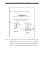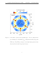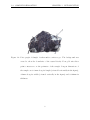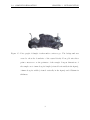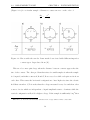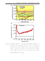
1
Design of Resistivity Instrumentation
for a He3 Cryostat and its Application
to the Charge Density Wave
Superconductor CuxTiSe2
by
Jason Iwachow
B.Sc., University of Waterloo, 2011
A THESIS SUBMITTED IN PARTIAL FULFILMENT OF
THE REQUIREMENTS FOR THE DEGREE OF
MASTER OF SCIENCE
in
The Faculty of Mathematics and Sciences
Department of Physics
BROCK UNIVERSITY
January 21, 2014
c
2014 Jason
Iwachow
Abstract
Fermi patches in quasi-two dimensional charge density waves (CDW) have not described
the connection to superconductivity (SC) according to theory adequately at this point
in time. The connection between CDW and SC in the quasi-two dimensional material
Cux TiSe2 is an interesting one which might reveal mechanisms in unconventional superconductors. A previous Brock graduate student grew crystals of Cux TiSe2 . The precise
doping of the samples was not known. In order to determine the doping parameter x in
Cux TiSe2 , a sensitive resistivity measurement system was necessary. A new resistivity
measurement system was designed and implemented utilizing an Infrared Labs HDL-10
He3 cryostat. By comparing with data from the literature, doping of two samples was
investigated using the new measurement system and a Quantum Design Magnetic Property Measurement System (MPMS). Methods for determining the doping revealed that
the old resistivity system would not be able to determine the CDW transition temperature of highly doped samples or doping for elongated samples due to electronic noise.
Doping in one sample was found to be between x=0.06 and x=0.065. Values of doping
in the second sample had a discrepancy but could be explained by incorrect sample
i
CHAPTER 0. ABSTRACT
orientation.
ii
Contents
Abstract
i
Glossary
v
Acknowledgements
xiii
1. Introduction
1
1.1. Crystal structure of Cux TiSe2 . . . . . . . . . . . . . . . . . . . . . . . .
4
1.2. Sample Preparation . . . . . . . . . . . . . . . . . . . . . . . . . . . . . .
7
2. Instrumentation
10
2.1. Principle . . . . . . . . . . . . . . . . . . . . . . . . . . . . . . . . . . . .
11
2.2. Measurement Noise . . . . . . . . . . . . . . . . . . . . . . . . . . . . . .
13
2.2.1. Contact Problems . . . . . . . . . . . . . . . . . . . . . . . . . . .
13
2.2.2. Instrument Noise . . . . . . . . . . . . . . . . . . . . . . . . . . .
15
2.2.3. Nyquist Noise . . . . . . . . . . . . . . . . . . . . . . . . . . . . .
15
2.2.4. Thermoelectric Effects . . . . . . . . . . . . . . . . . . . . . . . .
16
iii
Contents
Contents
2.2.5. Electromagnetic Noise . . . . . . . . . . . . . . . . . . . . . . . .
17
2.3. Design and Method . . . . . . . . . . . . . . . . . . . . . . . . . . . . . .
19
2.3.1. The Cryostat . . . . . . . . . . . . . . . . . . . . . . . . . . . . .
20
2.3.2. Sample holder . . . . . . . . . . . . . . . . . . . . . . . . . . . . .
22
2.3.3. Measuring Circuit . . . . . . . . . . . . . . . . . . . . . . . . . . .
23
2.3.4. Computer Data Acquisition . . . . . . . . . . . . . . . . . . . . .
26
3. Theory
28
3.1. Superconductivity . . . . . . . . . . . . . . . . . . . . . . . . . . . . . . .
29
3.2. Charge Density Waves . . . . . . . . . . . . . . . . . . . . . . . . . . . .
33
4. Magnetic Properties of Cux TiSe2
37
5. DC Transport Properties of Cux TiSe2
43
6. Conclusions
51
7. Future Research Directions
55
7.1. Magneto-optical . . . . . . . . . . . . . . . . . . . . . . . . . . . . . . . .
56
A. Pressure Induced Noise
58
B. GPIB Communication
62
C. Program Interface
65
iv
Glossary
AC
Alternating Current
API
Application Programming Interface
BCS
J. Bardeen, L. N. Cooper, and J.R. Schrieffer Theory of Superconductivitiy
CDW
Charge Density Wave(s)
DC
Direct Current
EMF
Electromotive force
GPIB
General Purpose Interface Bus, specified by the IEEE-488 standard
IC SIP
Integrated Circuit Single Inline Package
MPMS
Quantum Design Magnetic Property Measurement System
RF
Radio frequncy, specifically electromagnetic waves in the radio spectrum
RMS
Root Mean Squared
SC
Superconductivity
SQUID
Superconducting Quantum Interference Device
VDP
Van der Pauw
v
List of Figures
1.1. The phase diagram of Cux TiSe2 . Shows as doping of copper increases,
CDW disappears in favor of SC states. Note that there is a region of
coexistence. The inset is the crystal lattice of Cux TiSe2 . Reproduced
from [5]. . . . . . . . . . . . . . . . . . . . . . . . . . . . . . . . . . . . .
3
1.2. Crystal structure of 1T -TiSe2 . a) Cross sectional view of the lattice layers
showing relative positions. Layers X’ and X are chalcogen atoms and M
is the transition metal b) Octahedral form of the 1T phase of the lattice
where the chalcogen is Selenium and the metal is Titanium. Reproduced
from [9]. . . . . . . . . . . . . . . . . . . . . . . . . . . . . . . . . . . . .
5
1.3. Joint density of states in 2D momentum space of the two dimensional
superconducting (Tc =2.3K) CDW (TCDW =65K) material 2H-Nax TaS2
in the CDW state. The CDWs are situated on the high density patches
~1 , Q
~2 and Q
~3 . Reproduced from [6]. . . . . . . . . .
in three directions Q
vi
6
List of Figures
List of Figures
1.4. Photograph of Sample 1 taken under a microscope. The background
was erased to show the boundaries of the crystal clearly. Four gold wire
silver paint contacts are on the perimeter of the sample. Largest dimensions of the sample are 6.0 mm along its length (oriented horizontally in
the figure), 4.1mm along its width (oriented vertically in the figure) and
0.344mm in thickness. . . . . . . . . . . . . . . . . . . . . . . . . . . . .
8
1.5. Photograph of Sample 2 taken under a microscope. The background
was erased to show the boundaries of the crystal clearly. Four gold wire
silver paint contacts are on the perimeter of the sample. Largest dimensions of the sample are 6.9 mm along its length (oriented horizontally in
the figure), 3.0mm along its width (oriented vertically in the figure) and
0.700mm in thickness. . . . . . . . . . . . . . . . . . . . . . . . . . . . .
9
2.1. Top view of an arbitrary shape of uniform thickness with point contacts
labeled A,B,C, and D which can be used with the van der Pauw method.
11
2.2. Errors with the van der Pauw method associated with different imperfect
contact types. Reproduced from [11]. . . . . . . . . . . . . . . . . . . . .
14
2.3. a) Two insulated conductors twisted together to form a twisted pair signal
line. The arrows indicate an example for the direction of the current. b)
shows how the twists create spaces of opposite vector areas such that the
induction in one twist is canceled out by the next for a magnetic field
spatially uniform in that region. Reproduced from [18] . . . . . . . . . .
vii
19
List of Figures
List of Figures
2.4. The schematic of the Infrared Labs HDL-10 He3 cryostat. Modified from
[19]. Sample holder was mounted on the bolometer stage. . . . . . . . . .
21
2.5. The sample holder that is used inside the cryostat. Samples are mounted
with glue onto the copper plate at positions A and C. Sample one is at
A and sample two is at C. At position B there is a Lakeshore DT-670
silicon diode temperature sensor mounted with indium solder. Used as
the B sensor in the temperture controller. (see main text at sections 2.3.2
and 2.3.3) . . . . . . . . . . . . . . . . . . . . . . . . . . . . . . . . . . .
23
2.6. The block diagram of the resistivity setup. Voltage sources specified are
power supply equipment that were made at Brock University’s Electronics
Shop. The HP 34970A data acquisition switch unit utilized an HP 34903A
20 channel actuator general purpose switch card with a custom backplate
that housed the plugs. . . . . . . . . . . . . . . . . . . . . . . . . . . . .
25
3.1. Temperature dependence of the gap function. Reproduced from [25] . . .
32
3.2. Wavevector dependent Lindhard response function for a one-, two- and
three-dimensional free electron gas at zero temperature. Reproduced from
[3]. . . . . . . . . . . . . . . . . . . . . . . . . . . . . . . . . . . . . . . .
34
3.3. a) The charge density on a one-dimensional lattice, and below it, the
dispersion relation of a free electron model of a metal. b) In the CDW
state the lattice and charge density has a static periodic distortion. Below,
it shows that a gap of size ∆ opens in the dispersion relation. Reproduced
from [3]. . . . . . . . . . . . . . . . . . . . . . . . . . . . . . . . . . . . .
viii
35
List of Figures
List of Figures
3.4. Acoustic phonon dispersion relation of one-, two-, and three-dimensional
metals. Reproduced from [3]. . . . . . . . . . . . . . . . . . . . . . . . .
36
4.1. Temperature dependence of the magnetic susceptibility in Cux TiSe2 for
a field strength of 0.5T. a) Results from E. Moroson et al. [5]. b) Results
from Sample 1. Absolute value was shifted down due to diamagnetic
contribution from the capsule and grease used to hold the sample. Shows
the CDW transition temperature at ≈ 120 K . . . . . . . . . . . . . . . .
39
4.2. Temperature dependence of the magnetic susceptibility in Cux TiSe2 for
low field strength around the SC transition. a) Polycrystalline data from
E. Morosan et al. [5] at 5 Oe. b) Sample 1 (a single crystal) magnetization
for a field strength of 10 Oe. SC is observed with an onset at ∼ 3.6K. . .
41
4.3. Temperature dependence of the magnetic susceptibility in Cux TiSe2 for
low field strength around the SC transition. a) Polycrystalline data from
E. Morosan et al. [5] at 5 Oe. b) Sample 2 (a single crystal) magnetization
for a field strength of 10 Oe. SC observed with an onset at ∼ 2.5K. . . .
42
5.1. Temperature dependence of the resistivity in Cux TiSe2 . a) Results for
different dopings on single crystal samples in the a-b plane reproduced
from [8]. b) Resistivity of Sample 1 measured in the new resistivity system. Shows a CDW transition temperature of ≈ 162K. The dotted line
is a power law forced fit that emphasizes the CDW bump. . . . . . . . .
ix
44
List of Figures
List of Figures
5.2. Resistivity of Sample 1. The top left inset shows the first derivative of
the data. The bottom right inset shows the second derivative of the data.
The CDW feature is not visible beyond the first derivative. . . . . . . . .
46
5.3. Polynomial baseline fit on resistivity data for Sample 1. There is a clear
common dip at 161K which could be the CDW transition. a) Seventh
order. b) Tenth order. c) 20th order. . . . . . . . . . . . . . . . . . . . .
47
5.4. Tenth order polynomial baseline fit on resistivity data measured on old
resistivity system for Sample 1. Notice the peak to peak noise is magnitudes of order higher (up to 101.5 higher). Note that the peak is still
faintly visibly in the inset tenth order poloynomial base line fit at 161k,
however other features on this graph could easily be mistaken for the same
transition. . . . . . . . . . . . . . . . . . . . . . . . . . . . . . . . . . . .
48
5.5. Temperature dependence of resistivity in Sample 2, Cux TiSe2 in the two
different systems. a) Results in the old measurement system from liquid
nitrogen temperatures. b) Results in the new resistivity measurement
system from liquid He4 temperatures. Inset shows a 20th order polynomial
baseline fit showing a CDW transition of 166 K . . . . . . . . . . . . . .
x
50
List of Figures
List of Figures
6.1. Temperature dependence of the magnetic susceptibility in Cux TiSe2 for
a field strength of 0.5T for Sample 1. Absolute value was shifted down
due to diamagnetic contribution from the capsule and grease used to hold
the sample. Shows the CDW transition temperature at ≈ 120 K and
identifies the CDW transition temperature as identified by the resistivity
measurements at ≈ 162 K. There is a small feature around 162 K (see
inset for expanded view) which might identify as the CDW transition
temperature if the measurement was conducted with more resolution in
that region. . . . . . . . . . . . . . . . . . . . . . . . . . . . . . . . . . .
52
7.1. Photograph of the part of the magneto-optic measurement device that
will rotate two large neodymium magnets around the sample inside the
cryostat. Designed by Jason Iwachow. . . . . . . . . . . . . . . . . . . . .
57
A.1. Cool down data in the previous resistivity measurement system using the
same HDL-10 He3 cryostat on Sample 1. Notice the jumps at 300 K when
liquid N2 is filled and ∼77 K when liquid He4 begins to transfer into the
main vessel. . . . . . . . . . . . . . . . . . . . . . . . . . . . . . . . . . .
59
A.2. Room temperature (∼295 K) voltage measurement on a steel disk in the
current resistivity measurement system. At 1150s into the measurement
the vacuum pump was turned on. . . . . . . . . . . . . . . . . . . . . . .
xi
60
List of Figures
List of Figures
A.3. Room temperature (∼295 K) voltage measurement for a shorted contact
on the sample plug inside the cryostat. Vacuum was introduced at 3740s,
where a voltage spike is introduced. Atmospheric pressure was observed
at 7460s, which shows a voltage spike of opposite direction. . . . . . . . .
61
B.1. Configurations that GPIB can take on. a) Linear configuration also known
as daisy chain configuration. b) Star configuration. Reproduced from [37]
63
B.2. GPIB female connector with pins numbered. . . . . . . . . . . . . . . . .
63
C.1. A screen shot of the resistivity measurement system program main form.
Right Panel is the graphing area, upper left panel is the experiment parameters, and lower left is the type of measurement to perform. . . . . .
66
C.2. A screen shot of the resistivity measurement system program diagnostics
screen. The tab that is selected shows a diagram of the circuit inside the
HP 34903A switch card as well and multiple commands to diagnose the
source of a problem. . . . . . . . . . . . . . . . . . . . . . . . . . . . . .
67
C.3. A screenshot of the resistivity measurement system program machine settings screen. Instruments may be swapped out or replaced, while the
program can still operate. . . . . . . . . . . . . . . . . . . . . . . . . . .
xii
68
Acknowledgements
Dr. Maureen Reedyk
For her stress free guidance throughout my studies
Xiao Peng and Yang Pan
For introducing me to the instruments in the lab when I was new to Brock University
Jason Manson
For his help in theoretical concepts and with experimental debugging
And to my wife, Megan
For her constant support and understanding during those months of perpetual work.
xiii
1. Introduction
Superconductivity (SC) had been theorized to come about by electron electron interactions in 1957 by Bardeen, Cooper, and Schrieffer (BCS) [1]. A similar phenomena,
the charge density wave (CDW), was postulated to exist by Frölich in 1954 based on
electron hole interactions [2]. These two phenomena are quite similar in principle but
the CDW leads to an insulating condensate because the pair is charge neutral while in
SC the pair has a charge of 2e. The theory behind CDW requires that the system is
quasi-one-dimensional in order for the electron hole pairs to cause the Lindhard response
function to diverge around ±kf , a process called nesting [3]. In 1974 it was discovered
that anomalous properties of TaSe2 and TaS2 , which are quasi 2D systems, are due to
CDW’s [4]. Cux TiSe2 is also a quasi-two-dimensional material which exhibits the CDW
state [5]. Cux TiSe2 also exhibits a superconducting phase that has a varying Tc based
on the doping (parameter x) which seems to take over the CDW state. D. W. Shen et al.
[6] discuss the possibility that flat portions at the Fermi energy in two dimensions in the
first Brillouin zone can allow for such nesting (called Fermi patches) to occur for three
directions in the a-b plane [6]. However, theory still fails to explain why CDW’s appear
1
CHAPTER 1. INTRODUCTION
to compete with SC states, the phase diagram of the material, or why an anisotropic
gap can occur for SC when BCS predicts an isotropic gap [7]. The connection between
SC and CDW is of valuable interest in seeking the answers to the problems associated
with understanding unconventional superconductors.
Measurements on the previous resistivity measurement system were too noisy to determine the CDW transition temperature in crystals of Cux TiSe2 . In order to make
investigations of the properties of Cux TiSe2 , it was necessary to construct a resistivity
measurement system which could accurately measure the resistivity to detect the transition in and out of the CDW state as well as the SC transition. This system has been
realized and utilized to determine the doping concentration x in Cux TiSe2 which was
not possible before. Noisy measurement systems require stronger applied currents which
affect the values that are of interest. The previous system, based on Infrared Lab’s HDL10 He3 Cryostat, that was intended for optical measurements, was adapted haphazardly
by previous graduate students with little attention to noise protection in the system.
Additional measurement capabilities which were lacking on the previous design were
also incorporated. Measurement of multiple samples was implemented which conserves
liquid helium and time. The Hall effect measurement capability was also introduced
with the new design, and could be used to probe the charge of the carriers; thus probe
for a CDW transition [5].
2
CHAPTER 1. INTRODUCTION
Figure 1.1.: The phase diagram of Cux TiSe2 . Shows as doping of copper increases, CDW
disappears in favor of SC states. Note that there is a region of coexistence.
The inset is the crystal lattice of Cux TiSe2 . Reproduced from [5].
3
1.1. CRYSTAL STRUCTURE OF CUX TISE2
CHAPTER 1. INTRODUCTION
1.1. Crystal structure of CuxTiSe2
The undoped crystal structure of TiSe2 belongs to a group of materials called chalcogenides, with the generic formula MT2 . M is a transition metal and T is a chalcogen
anion S, Se, or Te. They usually have one of two crystal structures, designated either 1T
or 2H phase [8]. Chalcogenides are layered compounds where the layers are held together
by van der Waals forces. In the 1T phase, the Ti atoms are in octahedral coordination
with Se, shown in Figure 1.2 b), to produce a trigonal octahedral crystal (shown in inset
of Figure 1.1. The layers X’ and X are the chalcogens and M is the transition metal. The
layers X and X’ are two-dimensional hexagonal lattices where the X’ layer is parallel and
rotated 60 degrees relative to the X layer. In the 2H phase the layers are stacked (using
notation from Figure 1.2) X’MX’ XMX instead of X’MX X’MX, producing a trigonal
prismatic structure.
TiSe2 takes on the 1T phase. It is between the layers, the area held together by the
van der Waals force, that the copper dopant is intercalated causing expansion of the
unit cell in the a and c direction. This expansion is linear until it becomes constant for
dopant concentration x≥0.11 [5]. The structure shows clear quasi-two-dimensionality,
and this results in a quasi-two-dimensional CDW. The CDW in two dimensions occurs by
nesting on flat portions, called “Fermi patches” at the Fermi energy in the first Brillouin
zone [5]. As an example, Figure 1.3 shows the 2D Fermi patches in the joint density
of states of 2H-Nax TaS2 , another superconducting CDW material. The van der Waals
forces are weak compared to the bonding in the crystal which makes determination of
the orientation of the crystal for this material relatively easy by the rough method of
4
1.1. CRYSTAL STRUCTURE OF CUX TISE2
CHAPTER 1. INTRODUCTION
Figure 1.2.: Crystal structure of 1T -TiSe2 . a) Cross sectional view of the lattice layers
showing relative positions. Layers X’ and X are chalcogen atoms and M is
the transition metal b) Octahedral form of the 1T phase of the lattice where
the chalcogen is Selenium and the metal is Titanium. Reproduced from [9].
5
1.1. CRYSTAL STRUCTURE OF CUX TISE2
CHAPTER 1. INTRODUCTION
Figure 1.3.: Joint density of states in 2D momentum space of the two dimensional superconducting (Tc =2.3K) CDW (TCDW =65K) material 2H-Nax TaS2 in the
CDW state. The CDWs are situated on the high density patches in three
~1 , Q
~2 and Q
~3 . Reproduced from [6].
directions Q
6
1.2. SAMPLE PREPARATION
CHAPTER 1. INTRODUCTION
checking the plane which is easiest to cleave. This will be parallel to the a-b plane.
1.2. Sample Preparation
Batches of single Cux TiSe2 crystals were grown by Artorix de la Cruz de Ona at Brock
University using the iodine-vapour transport method as described by Wu et. al. [8].
Large crystals were selected to be able to conduct measurements easily and for future
optical spectroscopy research that yields stronger signals for larger reflective sample
surfaces. Two large single crystal samples were selected to be measured. Sample 1 was
the largest out of these and is shown in Figure 1.4. Sample 2 is elongated and shows
the silver paint contacts to be quite close to each other on either end of the sample as
seen in Figure 1.5. Both Figures 1.4 and 1.5 show the silver paint contacts for resistivity
measurement whose dimensions can be seen to be a significant fraction of the distance
between contacts. The consequences of this will be discussed later in section 2.2.1.
7
1.2. SAMPLE PREPARATION
CHAPTER 1. INTRODUCTION
Figure 1.4.: Photograph of Sample 1 taken under a microscope. The background was
erased to show the boundaries of the crystal clearly. Four gold wire silver
paint contacts are on the perimeter of the sample. Largest dimensions of
the sample are 6.0 mm along its length (oriented horizontally in the figure),
4.1mm along its width (oriented vertically in the figure) and 0.344mm in
thickness.
8
1.2. SAMPLE PREPARATION
CHAPTER 1. INTRODUCTION
Figure 1.5.: Photograph of Sample 2 taken under a microscope. The background was
erased to show the boundaries of the crystal clearly. Four gold wire silver
paint contacts are on the perimeter of the sample. Largest dimensions of
the sample are 6.9 mm along its length (oriented horizontally in the figure),
3.0mm along its width (oriented vertically in the figure) and 0.700mm in
thickness.
9
2. Instrumentation
A resistivity measurement system was greatly improved upon and further developed
in order to conduct more accurate and reliable measurements. The original set up
consisted of nano volt meter, nano current source, actuator switch connected into the
cryostat through various connection boxes, where the instruments were controlled with
GPIB (IEEE488) through a macro for the MPMS MultiVu program. The distribution
box for connections into the cryostat was made by Infrared Labs.
An input line was used for setup conditions and data was recorded to a file which
MultiVu reported. This original resistivity instrumentation produced noisy results due
to the system being unshielded and cluttered by redundant and insecure connections.
The software implementation was also crude and gave little information to the details of
the measurement and no chance of diagnosing problems. Noise levels were on the order
of 15 nVRM S . Contributions to this noise were from the instruments, Nyquist noise,
magnetic and RF sources. The new system implementation has reduced noise in the
system by a factor of 3.
10
2.1. PRINCIPLE
CHAPTER 2. INSTRUMENTATION
2.1. Principle
Instrumentation was designed to implement multiple sample resistivity or Hall effect
measurements by the van der Pauw method. In 1958 L. J. van der Pauw showed that
resistivity or the Hall coefficient of an arbitrary shape can be measured by a four contact
measurement if the sample is thin and of uniform thickness, contacts are small, contacts
are on the circumference, and the sample contain no holes [10]. Consider the arbitrary
shaped sample of small uniform thickness in Figure 2.1.
Figure 2.1.: Top view of an arbitrary shape of uniform thickness with point contacts
labeled A,B,C, and D which can be used with the van der Pauw method.
If we apply a current to A (positive) and B (negative), IAB , and measure the voltage
at D (positive) and C (negative), VDC , then we can define the resistance:
RAB,DC =
VDC
IAB
We can call this resistance measurement the “horizontal” configuration. Similarly for
current on B,C and voltage reading on A,D gives RAD,BC (similarly called the “vertical”
11
2.1. PRINCIPLE
CHAPTER 2. INSTRUMENTATION
configuration), then the resistivity of the sample can be shown [10] to be:
e
−πRAB,DC d
ρ
+e
−πRAD,BC d
ρ
=1
(2.1)
Where ρ is the resistivity of the material and d is the thickness. There is practical further
improvement to this measurement. By reversing the current in each configuration and
taking the average of each, any DC offset present in the system can be canceled out.
Taking the averages for the resistances in their respective configurations:
Rhorz =
RAB,DC − RBA,DC
2
Rvert =
RAD,BC − RDA,BC
2
Gives us a more reliable value for those resistances. Equation 2.1 becomes
e
−πRhorz d
ρ
+e
−πRvert d
ρ
=1
(2.2)
A Hall effect measurement using the setup to be described can be done by applying
current on A,C and measuring the voltage change on D,B as a uniform magnetic field is
applied perpendicularly to the surface and then reversed in direction [11]:
RH =
d · ∆VDB
B · IAC
(2.3)
Where RH is the Hall coefficient and B is the magnitude of the magnetic field1 .
1
not to be confused with the subscript B which represents the contact across which the voltage is
being measured.
12
2.2. MEASUREMENT NOISE
CHAPTER 2. INSTRUMENTATION
2.2. Measurement Noise
There were many different sources of noise that entered the system before it was improved. Noise levels prevent accurate measurements. Noise can drown out important
characteristics in data, reduce resolution and prevent valuable measurements of very
low resistance materials. In the work carried out for this thesis, sources of electromagnetic noise that were present in the system were suppressed using standard engineering
practices. Noise is typically measured in root mean squared (RMS) values of voltage
and power. The root mean squared value can be calculated for a set of data xn in the
following way:
xrms
v
u n
u1 X
(xn − x̄)2
=t
n 0
(2.4)
Where x̄ is the base line signal value. The noise that is of importance to the measurement
of resistivity is the noise associated with the voltage measurement.
2.2.1. Contact Problems
The van der Pauw method assumes that the contacts are very small compared to the
sample size and they occur at the circumference of the material. When measuring a
sample which is less than about 0.5mm in its largest dimension, the contact size becomes
a problem.
The estimation of error [11] in resistivity ∆ρ deviating from the true value ρ for a
length along the circumference l (Figure 2.2 a), a strip length l of contact from the
circumference (Figure 2.2 b), or a contact a distance l away from the circumference
13
2.2. MEASUREMENT NOISE
CHAPTER 2. INSTRUMENTATION
(Figure 2.2 c) for a circular sample of diameter ø causes an error on the order of
∆ρ
−l2
∼ 2
ρ
ø ln(2)
Figure 2.2.: Errors with the van der Pauw method associated with different imperfect
contact types. Reproduced from [11].
This error becomes quite large when the distance between contacts approaches the
size of the contact. The other problem that arises for small samples is when the sample
is elongated, such that contacts A,B and C,D are very close while each pair are far from
each other. This causes the horizontal configuration to have high noise since the electric
field that extends to C,D is weak; thus the voltage measured is very low and then other
sources of noise which are independent of signal amplitude start to dominate while the
vertical configuration will yield a higher voltage. If the sample is sufficiently long2 then
2
When LA,D LA,B the van der Pauw derivation is no longer valid for finite contact size.
14
2.2. MEASUREMENT NOISE
CHAPTER 2. INSTRUMENTATION
the resistivity can be approximated to that of a two contact measurement with four
leads.
2.2.2. Instrument Noise
In reality instruments for measurement never meet the ideal case which is discussed in
theory. In the case of a voltmeter, it ideally has infinite impedance and measures the
voltage exactly without noise. However, in order to do a measurement of voltage, some
current must be drawn and thus presents a finite impedance. Even more problematic,
measurement devices involve their own circuitry that introduces its own sources of noise,
in particular thermal agitation noise in transistors. This sets a lower bound on the noise
level that can be achieved. Noise levels are usually given by the manufacturer in the
specifications, however in this thesis work they were measured to confirm them and
identify other sources of noise.
2.2.3. Nyquist Noise
Nyquist noise, discovered by Johnson in 1928 [12] is noise that arises in a circuit due
to charge carriers in thermal equilibrium, which are in a state of permanent thermal
agitation [13]. Nyquist noise is voltage fluctuations that occur (on average) uniformly
over the whole frequency spectrum3 , called white noise [13]. The equation is given by:
VRM S =
3
p
4kB T R∆f
(2.5)
The spectral density of Nyquist noise is constant up to the angular frequency corresponding with the
correlation time ∼ 1014 s−1 , see bibliography entry [13].
15
2.2. MEASUREMENT NOISE
CHAPTER 2. INSTRUMENTATION
Where VRM S is the RMS noise of the voltage in the conductor in the frequency bandwidth ∆f , R is the resistance in ohms, T is the temperature in Kelvin and kB is the
Boltzmann constant [14]. We are interested in making DC measurements and ideally
the bandwidth is zero, but no DC measurement is purely DC since there is always a time
range of measurement which sets the bandwidth. Therefore, the noise that arises in the
measurement from Nyquist noise is unavoidable at some level since the measurement is
always carried out at finite temperature. This means that the measurement leads and
the material that is being measured are likely to contribute the most Nyquist noise.
2.2.4. Thermoelectric Effects
Thermoelectric generation effects occur when there is a temperature difference across
two contacts in a circuit that are made of different conductors (specifically with different
Seebeck Coefficients). Thermoelectric voltages are generated when there is an electrochemical potential in the circuit and are created by a thermal gradient [13]. The voltage
generated is defined as
Eemf = −S∆T
(2.6)
where S is the Seebeck coefficient and ∆T is the difference in temperature between
the contacts [15]. In order to cancel these effects for equilibrium conditions resistance
is measured by applying current in both directions and averaging the results. However,
these effects can have an impact on the measurement while temperature is changing.
The time dependent version of the Seebeck equation (equation 2.6) for a delay τ in
16
2.2. MEASUREMENT NOISE
CHAPTER 2. INSTRUMENTATION
measuring positive and negative current is given by:
Z
V = −S
τ
∆
0
dT
dT
dt ≈ −S∆ τ
dt
dt
(2.7)
In the Infrared Labs HDL-10 He3 cryostat (henceforth to be referred to as “the cryostat”), the largest Seebeck coefficient difference of any signal carrying wires is 40 µV/K
(Constantan and Copper at room temperature). If we estimate that the rate of cooling
is 0.2 K/s, and modestly estimate the Leidenfrost point for liquid nitrogen is 277K in
the cryostat4 , we obtain a value of a time dependent thermoelectric voltage of about
16mV. This is highly significant for materials being measured with very low currents
or very low resistivities. However, for warm up times that take days this value is on
the order of 10−10 V. This means that cool down measurements are very untrustworthy
while for warm up measurements this is a very minimal contribution to measurement
signal disturbance.
2.2.5. Electromagnetic Noise
The environment has many sources of magnetic fields, electric fields and electromagnetic
fields. Radio frequency (RF) noise is naturally present in the environment and is easiest
to reduce. RF noise comes from space, man made sources for telecommunication, as well
as from undesired radiation sources such as paired signal lines that have bends, terminations or discontinuities [16]. These sources that are present in the environment, present
a source of noise in the lab by absorption into signal transmission lines that are not
properly shielded. RF noise can be effectively removed from the system by“wrapping”
4
The rate of cooling is greatest below the Leidenfrost point because there is no insulating vapor blanket.
17
2.2. MEASUREMENT NOISE
CHAPTER 2. INSTRUMENTATION
all of the signal lines used with a conductor that is grounded. This grounded shield
prevents signals entering the system by acting as a reflector and Faraday cage. This
blocks both RF signals and electrostatic fields. A coaxial cable is a typical example
of the implementation of this idea, and is used in this resistivity measurement system.
Magnetic noise, however, is more difficult to block. Slowly varying magnetic fields such
as those from an AC power distribution5 , the Earth, or a vibrating ferromagnetic material will penetrate Faraday cages. A straight transmission pair will have a gap between
the conductors, and if a varying magnetic field is present, the flux through that area
will induce a voltage. One solution to this problem is to surround the signal lines with
a high permeability material to “redirect” the field lines away from the signal lines, an
example product being MuMetal [17]. The magnetic field does not need to be zero inside
this region; there is an alternative solution.
Consider a transmission line that consists of two twisted wires as shown in Figure 2.3
a). If we assume the source of the varying magnetic field to be sufficiently far so that
the field is almost uniform around the twisted pair, and the twists to be approximately
the same spacing, then for any direction of the magnetic field the flux in each twist
will be equal and opposite to adjacent ones. This will cause an EMF to be induced in
equal yet opposite directions and therefore cancel out, shown in Figure 2.3 b). Cables
using twisted pairs inside a braided metal sleeve that is grounded remove most of both
RF and slowly varying magnetic fields. This is implemented everywhere possible in the
resistivity system that was designed for this thesis work.
5
Referring to power for buildings in north America 120VRM S at 60Hz.
18
2.3. DESIGN AND METHOD
CHAPTER 2. INSTRUMENTATION
Figure 2.3.: a) Two insulated conductors twisted together to form a twisted pair signal
line. The arrows indicate an example for the direction of the current. b)
shows how the twists create spaces of opposite vector areas such that the induction in one twist is canceled out by the next for a magnetic field spatially
uniform in that region. Reproduced from [18]
2.3. Design and Method
The instrument design consisted of three basic components. The sample was mounted
on a holder inside the Infrared Labs HDL-10 He3 cryostat. The connections led to a
32 pin connector that in turn led to the distribution box where the instruments were
connected. The information from the instruments was then read through IEEE-488
(known as GPIB) communication to the computer where the data was collected in the
resistivity program.
19
2.3. DESIGN AND METHOD
CHAPTER 2. INSTRUMENTATION
2.3.1. The Cryostat
The cryostat is where the sample resides and which provides an environment that can
potentially reach temperatures of ∼ 0.4 degrees Kelvin. The sample holder is mounted
on either the bolometer stage or sample stage (see Figure 2.4). Spare connections inside
the cryostat were utilized for resistivity connections by installing 6 pin IC SIP plugs.
Once the sample holder is mounted and plugged in, the cryostat is sealed and evacuated
to pressures on the order of 1 · 10−6 Torr. Thermal radiation shielding is maintained
by filling the shield vessel (nitrogen vessel that is thermally connected with the shield)
with liquid nitrogen. Cooling is achieved by filling the main vessel (helium vessel which
is thermally connected with the cold plate) with liquid nitrogen first. This is then
replaced with liquid He4 . Liquid Nitrogen precooling reduces liquid helium boil off
during the transfer. Evacuating the vessel (pumping) can lower the temperature to ∼
2K, below which then the He3 one shot refrigerator is utilized to go to as low as ∼ 0.4
degrees Kelvin. He3 refrigeration is achieved by the following steps. The He3 tank is
connected through a valve to a charcoal pump. The He3 tank valve is opened, allowing
absorption of He3 in the charcoal pump at the He4 boiling point. A thermal switch is
opened to thermally isolate the pump from the cold plate and sample, and the He3 tank
valve is closed trapping the He3 gas. Heat is applied to the charcoal pump to raise its
temperature. The power is turned off at around 40K, and the thermal switch to the stage
where the sample holder is mounted is closed, allowing the He3 vapour to condense in a
vessel thermally connected to the stage on which the sample holder is mounted cooling
it to as low as ∼ 0.4K when the charcoal pump is cooled to allow it to pump on the
20
2.3. DESIGN AND METHOD
CHAPTER 2. INSTRUMENTATION
Figure 2.4.: The schematic of the Infrared Labs HDL-10 He3 cryostat. Modified from
[19]. Sample holder was mounted on the bolometer stage.
21
2.3. DESIGN AND METHOD
CHAPTER 2. INSTRUMENTATION
condensed He3 . Temperature is not maintained at any point other than at the boiling
points of N2 and He4 . Temperature dependent data is taken by letting the system warm
up at its own pace. With the system evacuated and the thermal shield vessel depleted6
typical warm up times from 4 K to 300 K are on the order of 72 hours.
2.3.2. Sample holder
The sample holder was constructed to make mounting of samples easily interchangeable.
Figure 2.5 shows one empty sample holder. Samples are either glued with GC varnish,
epoxy or double sided tape into positions A and C. Gold wire is soldered to the copper
wires around those positions and the other end is made into a contact on the sample using
silver paint. Copper wires around the sample positions are placed so that orientation of
the contacts is unambiguous.
In the center, at position B, there is a Lakeshore DT-670 silicon diode temperature
sensor mounted to measure temperature for temperatures between 1.4 K - 500 K. There
are three temperature sensors built into the cryostat; Two sensors at the sample stage
(a B sensor for high temperature and an A sensor for low temperatures) and one in the
bolometer stage (an A sensor for low temperature). Two sensors are used to accurately
measure the full range of temperatures in the experiment (see section 2.3.3). In the
sample holder shown in Figure 2.5, the temperature sensor at position B is used as
the B sensor for the temperature controller. The bolometer stage has no sensor for
6
If the shield is not depleted thermal equilibrium will be maintained at the boiling point of liquid
nitrogen
22
2.3. DESIGN AND METHOD
CHAPTER 2. INSTRUMENTATION
Figure 2.5.: The sample holder that is used inside the cryostat. Samples are mounted
with glue onto the copper plate at positions A and C. Sample one is at A
and sample two is at C. At position B there is a Lakeshore DT-670 silicon
diode temperature sensor mounted with indium solder. Used as the B sensor
in the temperture controller. (see main text at sections 2.3.2 and 2.3.3)
the temperature range 6 K - 500 K. Mounting the temperature sensor directly on the
sample holder has the additional benefit of reducing error associate with reading the
temperature in thermal non-equilibrium for a temperature gradient between the sample
and the sensor.
2.3.3. Measuring Circuit
The block diagram of the measuring instrument circuit is shown in Figure 2.6. The
32 pin connector from the cryostat goes into the distribution box which breaks out to
all the instruments. The temperature is measured through the Lakeshore DRC-91CA
temperature controller, which contains the data for the voltage - temperature curves.
It has two inputs, one for sensor A (the low temperature sensor) and one for B (the
23
2.3. DESIGN AND METHOD
CHAPTER 2. INSTRUMENTATION
high temperature sensor). The distribution box has a switch to control which A and B
sensor to read from, either bolometer or sample stage. The B sensor mounted within
the cryostat (the Lakeshore DT-470 silicon diode sensor) is only accurate to 6 K. The A
sensor (the Lakeshore GR200A germanium sensor) is accurate below this temperature
to about 0.3 K. With the DT-670 sensor used as the B sensor, the switch from A to B
sensor occurs at 1.4 K.
An HP 34420A nano volt meter and Keithley 6221 DC and AC current source are
connected with a 4 pin mini XLR cable utilizing the noise reduction methods described
earlier to the HP 34970A data acquisition/switch unit with an HP 34903A 20 channel
actuator general purpose switch card. The HP 34903A card in the switch unit allows
for the voltage (V+, V-) and current source (I+, I-) contacts to be arranged in any
permutation to the contacts A,B,C, and D on sample A or B. This allows for not only
resistivity measurements but also Hall effect measurements. From the switch unit, two 4
pin mini XLR cables, each representing the four contacts from one sample, are connected
to the distribution box. The three voltage sources in Figure 2.6 are connected to the
distribution box by BNC coaxial cables. These are power supply equipment that were
made at Brock University’s Electronics Shop. They manually control power to the
bolometer stage charcoal pump, sample stage charcoal pump, and cold plate heater. An
HP 34401A Multimeter is used to measure the resistance of the charcoal pumps, giving
a rough estimation of its temperature. A switch on the distribution box controls which
stage it is measuring.
24
2.3. DESIGN AND METHOD
CHAPTER 2. INSTRUMENTATION
Figure 2.6.: The block diagram of the resistivity setup. Voltage sources specified are
power supply equipment that were made at Brock University’s Electronics
Shop. The HP 34970A data acquisition switch unit utilized an HP 34903A
20 channel actuator general purpose switch card with a custom backplate
that housed the plugs.
25
2.3. DESIGN AND METHOD
Step
1
2
3
4
5
CHAPTER 2. INSTRUMENTATION
Instruction
Read Sample Temperature
Set Horizontal Configuration, Pause
Set Current, Pause then Read Voltage
Set Vertical Configuration, Pause
Set Current, Pause then Read Voltage
Table 2.1.: Basic program steps for a resistivity measurement. Setting configuration
occurs at the data switch unit
2.3.4. Computer Data Acquisition
The data from the instruments is read by the computer using IEEE-488 (also known
as GPIB) communication. The details of the communication are discussed in Appendix
B. Measurements are taken when both cooling and warming, however only the warm
up measurements are used for reasons discussed in section 2.2 on noise. The rate at
which data is read is limited by the speed of the instruments. The HP 34420A nano volt
meter has a built in function which integrates the measurement over a certain number
of power supply cycles [22]. At 10 cycles (which was used for all measurements taken)
a response time of ∼ 0.5 seconds is given. In order to assure that the relays in the HP
34903A 20 channel actuator general purpose switch card were at rest7 the measurement
loop was paused for 0.5s after each configuration change in the unit. The measurement
loop measures the resistivity in the basic steps outlined in table 2.1.
More time delay is introduced than shown by taking an average of several measurements for each configuration and due to the fact that this cycle is repeated for the second
sample at position C. On average, for a single sample measurement it takes ∼ 6 seconds
for a single van der Pauw measurement to be taken. As discussed before, this time is
7
Relays or switches tend to bounce when switched over, thus causing noise in the signal.
26
2.3. DESIGN AND METHOD
CHAPTER 2. INSTRUMENTATION
small compared to the thermal change in that time frame so noise is low, which also
implies that the temperatures are approximately equal to each other when measuring
each van der Pauw configuration. An averaging function is included in the program
which averages the values over whatever temperature range is specified. Since there are
many different instruments and connections, the program was made to include diagnostic tools to identify sources of troubles. Details of the program interface are included in
Appendix C.
27
3. Theory
Before discussing the theories describing CDW and SC materials, a brief review of magnetism is necessary to understand certain aspects of their properties. Remember that
the total magnetic dipole moment is defined as m
~ = I~a where I is the current and ~a is
the vector area [20]. A material may exhibit a magnetic field of its own without electrical
current when there are tiny dipole sources through out the material. If m
~ is the sum of
all these magnetic dipoles throughout the material, we define magnetization as
~
~ =m
M
X
Where X is a volume, mass or moles. For convenience, we will use the same units as the
magnetic measurement system uses (see chapter on magnetic properties). Magnetization
is measured in
emu
g
where
1emu = 10−3 A · m2
The auxiliary field is measured in Oersted (Oe).
1Oe =
1000 A
4π m
28
3.1. SUPERCONDUCTIVITY
CHAPTER 3. THEORY
The total magnetic field in space is the sum of the auxiliary field, H (fields caused
~ = µo ( H
~ +M
~ ). When the magnetization
by a current), and the magnetization by B
~ = χH
~ where χ is the magnetic
is a linear response in the auxiliary field we have M
susceptibility. Diamagnetism arises from orbital motion of the electrons and is present
in all materials, and in general is very weak. Diamagnetism has a field that opposes the
H field and therefore has negative susceptibility. Paramagnetism arises from the spin
of the electrons attempting to align to the H field, and can only do so when there are
unpaired electrons and is related to the density of states [21].
3.1. Superconductivity
Superconductivity is a state of matter for which the material has perfect conductivity
and exhibits perfect diamagnetism. The original phenomenological explanation of zero
resistance and the Meissner effect by the London brothers [23] was expanded by Pippard to the nonlocal generalized case[24]. Ginzburg and Landau in 1950 introduced the
theory of superconductivity based on characterizing the superconducting electrons by a
pseudo-wavefunction order parameter [25]. With this, spatial variations of the density of
superconducting electrons could be calculated. Finally, the microscopic theory of superconductivity was put forth by Bardeen, Cooper, and Schrieffer in 1957 [1]. BCS theory
predicted the isotope effect1 and predicted that electron pairs (mediated by phonons)
were responsible for superconductivity [1]. London showed[23] by taking the relaxation
1
The isotope effect is the change in the SC transition temperature based on the mass of the isotope
of superconducting material Tc ∝ M −α . [26]
29
3.1. SUPERCONDUCTIVITY
CHAPTER 3. THEORY
time to be infinite in the Drude model of conductivity that:
~ = ∂ (ΛJ~s )
E
∂t
(3.1)
where Λ is defined as
Λ=
4πλ2
m
=
2
c
ns e2
(3.2)
Here λ is called the London penetration depth, ns is the density of superconducting
electrons, e is the charge of the carrier, and m is the mass of the charge carrier. Equation
3.1 shows that for steady current, the electric field is zero. This is what we expect for
superconductivity. In the same paper London showed
~ = −c∇ × (ΛJ~s )
H
(3.3)
If we substitute 3.1 into 3.3 we obtain
~ =
∇2 H
~
H
λ2
(3.4)
A particular solution to 3.4 is for an infinite flat slab superconductor in the YZ plane,
~o
where the superconductor exists everywhere x > 0, and a magnetic field strength of H
exists everywhere outside the sample. The magnetic field inside the superconductor is
then given [27] as
~ =H
~ o e −x
λ
H(x)
which makes it clear why λ is described as the penetration depth, since it describes the
30
3.1. SUPERCONDUCTIVITY
CHAPTER 3. THEORY
penetration of a magnetic field into the superconductor. An important result follows
for a flat slab of thickness d; it can be shown that [25] when d λ the susceptibility
becomes:
M =−
Ho
.
4π
(3.5)
This perfect diamagnetism in superconductors is called the Meissner effect. The Meissner effect means that there is no magnetic field in the material which is implied by
London’s equations. The transition of the magnetization is sudden when entering the
superconducting state. There is however a critical field at which superconductivity is
lost [25] and which is approximated by Hc (T ) ≈ Hc(0)[1 − (T /Tc )2 ] where Tc is the
critical temperature. Abrikosov investigated a different limit of Ginzburg Landau theory2 and predicted that a mixed state might appear where the superconducting bulk
would contain an array of flux tubes with superconducting vortices around them and
cause a continuous transition in the magnetization instead [25]. This is called a type II
superconductor, and the susceptibility is perfectly diamagnetic until it enters this mixed
state at a critical field called Hc1 . It remains in the mixed state until a second critical
field called Hc2 , above which it reverts to the normal state.
BCS Theory predicts that superconductivity is created by Cooper pairs: pairs of
weakly attractive electrons mediated by phonons. BCS predicts the temperature dependent gap energy ∆(T ) which is the energy to break a Cooper pair [1]. The temperature
dependent gap function is shown in Figure 3.1.
2
He investigated what would happen if the Ginzburg Landau parameter κ were large instead of
small [25].
31
3.1. SUPERCONDUCTIVITY
CHAPTER 3. THEORY
Figure 3.1.: Temperature dependence of the gap function. Reproduced from [25]
The energy of the zero temperature gap in BCS theory can be determined by the
equation [28]
2∆(0) = 3.52kB Tc
(3.6)
where kB is the Boltzmann constant. The principle which the magnetic field breaks
the pair (or sufficiently high current to generate a field to break the pairs) is when
the landau splitting causes high enough energy to reach the gap energy (orbital vortex
pair breaking) [29] or Zeeman splitting when the field is strong enough to split the
energies sufficiently to exceed the gap energy (pauli pair breaking) [30][31]. So when
measuring the SC transition temperature, it is important to use low fields and currents
to prevent the Cooper pairs from breaking. The Meissner effect is utilized to find the
superconducting transition temperature by susceptibility measurements.
32
3.2. CHARGE DENSITY WAVES
CHAPTER 3. THEORY
3.2. Charge Density Waves
The concept of the charge density wave (CDW) was first theorized by Rudolf Peierls in
1930 [2]. A CDW is a periodic distortion of a quasi-one dimensional lattice producing
a static wave distortion in the charge density along the lattice [3]. The mechanism that
produces this distortion is an electron-hole condensate similar to the electron-electron
Cooper pair of BCS theory. Coincidentally, the Ginzburg Landau theory in the long
wavelength limit can be used to describe CDW [3]. One way to show how CDW comes
about is to consider the Lindhard theory of screening in one dimension. It arises by
considering a Schrödinger equation with a potential due to the lattice atoms and other
electrons with charge screening in a free electron gas [32]. In the case that the screening charge density is linear in the potential, the dielectric constant becomes (Lindhard
response function [3]):
Z
χ(~q) =
d~k fk − fk+q
(2π)d Ek − Ek+q
(3.7)
where fk is the fermi function at wavevector k, and χ is the dielectric susceptibility. If
this is integrated for three or two dimensional fermi surfaces of a free electron gas energy
Ek =
~2 k 2
2me
where me is the free electron mass, the result isn’t very interesting. However, integration
in one dimension around the Fermi energy3 leads to a divergence around q = 2kf [3].
The three situations are depicted in Figure 3.2:
3
linearized near the Fermi energy as Ek − EF = ~vf (k − kF ).
33
3.2. CHARGE DENSITY WAVES
CHAPTER 3. THEORY
Figure 3.2.: Wavevector dependent Lindhard response function for a one-, two- and
three-dimensional free electron gas at zero temperature. Reproduced from
[3].
This shows that there is a lowering of energy for an electron at −kF and hole at
+kF . This electron-hole pair produces a gap (thus reducing the energy) in the electronic
dispersion relation near ±kf . This new state causes a static periodic distortion of the
lattice and charge as shown in Figure 3.3
In 1959 Kohn proposed that CDW would cause a discontinuity in the phonon dispersion where a notch is formed around 2kf [33]. This is shown in Figure 3.4.
In CDW there is a gap function that describes the energy needed to destroy the pairs,
analogous to the BCS gap function. This gap function forms suddenly producing a
second order phase transition. In superconductivity, the Cooper pair has a net charge
34
3.2. CHARGE DENSITY WAVES
CHAPTER 3. THEORY
Figure 3.3.: a) The charge density on a one-dimensional lattice, and below it, the dispersion relation of a free electron model of a metal. b) In the CDW state the
lattice and charge density has a static periodic distortion. Below, it shows
that a gap of size ∆ opens in the dispersion relation. Reproduced from [3].
35
3.2. CHARGE DENSITY WAVES
CHAPTER 3. THEORY
Figure 3.4.: Acoustic phonon dispersion relation of one-, two-, and three-dimensional
metals. Reproduced from [3].
thus contributes to conduction. However, it is important to note that the electron-hole
pair bosonic quasi-particle (amplitudon) is charge neutral and has an interaction with
impurities and lattice imperfections, which causes it not to contribute to DC conduction.
The introduction of the gap however causes resistivity to increase. The onset of this
defines the CDW transition [3].
36
4. Magnetic Properties of CuxTiSe2
Several samples of Cux TiSe2 were selected from a crystal growth carried out by Artorix
de la Cruz de Ona at Brock University. The dopings of the samples were not known. In
order to test the resistivity system that was constructed, a set of DC magnetic susceptibility measurements were done on these samples to characterize their superconducting
transition temperatures. These measurements were conducted in a Quantum Design
Inc. Magnetic Property Measurement System (MPMS). The MPMS measures the susceptibility by applying a field, then physically transporting the sample through a set of
counter-wound coils, which pick up the change in induction measured with a SQUID.
The magnetic susceptibility is then calculated based on the EMF measured and corrected by a correlation table [34]. The temperature range of the MPMS is 1.9K - 400K
[34]. The sample was placed in a plastic capsule with some vacuum grease to prevent the
sample from moving while being transported in the MPMS and oriented such that the
~ field. Measurements were compared to results from E.
a-b plane was parallel to the H
Moroson et al. [5] to determine the doping concentration x. A temperature dependent
measurement was conducted at 0.5T field strength from 300 K to 1.8 K on sample 1,
37
CHAPTER 4. MAGNETIC PROPERTIES OF CUX TISE2
shown in Figure 4.1.
In Figure 4.1 a) it can be seen that at high temperature the susceptibility is positive
and then, as temperature decreases, drops at a certain temperature. This temperature
is the transition temperature into the CDW state which causes the susceptibility to
decrease once the gap in the dispersion relation is formed. This is because the electronic
density of states drops, and the contribution from Pauli paramagnetism is reduced, and
the core diamagnetism begins to dominate [5]. The magnetization then rises with CurieWeiss like behavior as temperature is further lowered until it drops to pure diamagnetism
below the SC transition temperature. Figure 4.1 b) shows the measurement on Sample
1. There appears to be a shift in the data to negative susceptibilities. This may have
been a diamagnetic shift due to an improper correlation table loaded in the MPMS to
account for the grease. However, the importance for determining the doping is in the
temperature dependent features and the absolute offset is not important. The data is
quite noisy but it can be approximated that the CDW transition temperature is around
120 K. Comparing Figure 4.1a) to 4.1 b) we can estimate the doping to be between
x=0.03 and x=0.04.
In small fields we can observe the SC transition at low temperatures to characterize
the doping of the sample. E. Morosan et. al. measured [5] the critical fields for polycrystalline Cu0.08 TiSe2 at 3.5 K to be Hc1 ≈ 18 Oe and Hc2 ≈ 3000 Oe. The zero temperature
values are Hc1 ≈ 0.12 T and Hc2 ≈ 1.33 T. In Sample 1, a field of 10 Oe was applied
parallel to the a-b plane to observe the SC transition. The results (shown in Figure 4.2)
show a SC transition temperature of about 3.6K. This suggests by comparison to data
38
CHAPTER 4. MAGNETIC PROPERTIES OF CUX TISE2
Figure 4.1.: Temperature dependence of the magnetic susceptibility in Cux TiSe2 for a
field strength of 0.5T. a) Results from E. Moroson et al. [5]. b) Results from
Sample 1. Absolute value was shifted down due to diamagnetic contribution
from the capsule and grease used to hold the sample. Shows the CDW
transition temperature at ≈ 120 K
39
CHAPTER 4. MAGNETIC PROPERTIES OF CUX TISE2
from Figure 4.2 a) that the doping is between x=0.06 and x=0.1.
A second sample (Sample 2) was also characterized for the SC transition with the field
of 10 Oe parallel to the a-b plane of the sample. The results are shown in Figure 4.3.
The SC transition temperature appears at about 2.5K which would suggest a doping
between x=0.055 and x=0.06.
The comparison of the results for the SC transition from E. Morosan et al. [5] to
measured data on Samples 1 and 2 is not ideal to characterize the doping. The SC
transition curves in Figures 4.2 b) and 4.3 b) do not seem to have the same slope as
the data of E. Morosan et al. [5]. This may be the result of having a range of doping
in a single crystal due to different doping concentrations in different regions of the
crystal causing a range of transition temperatures. E. Morosan et al. [5] performed
measurements on polycrystalline samples, which may behave differently than a single
crystal since all crystal orientations are taken into account with polycrystalline samples
while Samples 1 and 2 were measured with the H field parallel to the a-b plane. Notice
in Figures 4.2 a) and 4.3 a) that the transition temperature increases with doping from
x=0.55 to x=0.08. However, above doping of x=0.08 there seems to be a turning point,
which causes doping of x=0.10 to go to a lower SC transition temperature. It is not clear
from this measurement whether the doping is above or below the peak SC transition
temperature concentration. The result can however be compared to other measurement
techniques to find the doping to look for consistency.
40
CHAPTER 4. MAGNETIC PROPERTIES OF CUX TISE2
Figure 4.2.: Temperature dependence of the magnetic susceptibility in Cux TiSe2 for low
field strength around the SC transition. a) Polycrystalline data from E.
Morosan et al. [5] at 5 Oe. b) Sample 1 (a single crystal) magnetization for
a field strength of 10 Oe. SC is observed with an onset at ∼ 3.6K.
41
CHAPTER 4. MAGNETIC PROPERTIES OF CUX TISE2
Figure 4.3.: Temperature dependence of the magnetic susceptibility in Cux TiSe2 for low
field strength around the SC transition. a) Polycrystalline data from E.
Morosan et al. [5] at 5 Oe. b) Sample 2 (a single crystal) magnetization for
a field strength of 10 Oe. SC observed with an onset at ∼ 2.5K.
42
5. DC Transport Properties of
CuxTiSe2
Resistivity measurements were conducted in the a-b plane on the same samples of
Cux TiSe2 (as in the magnetic properties chapter) using the resistivity measurement
system constructed. The CDW transition temperature and SC transition temperature
was extracted. Measurements show a broad maximum which agrees with other groups
[8][5]. Low temperature measurements1 did not have the slow rate2 to obtain ideal low
noise measurements due to unforeseen technical difficulties. Time constraints did not
allow the measurements to be repeated. Typical contact resistance was between 3Ω and
12Ω. The results for Sample 1 are shown in Figure 5.1 b) with a power law forced fit to
emphasize the CDW bump.
In Figure 5.1 a), the CDW state produces an increase in resistivity manifesting in a
broad peak centered around 90 K. By comparison with the data shown in Figure 5.1
a), the doping of Sample 1 appears to be in the range of x=0.055 to about x=0.065.
1
Temperatures utilizing the He3 system on the cryostat.
2
Rate of change of temperature with time.
43
CHAPTER 5. DC TRANSPORT PROPERTIES OF CUX TISE2
Figure 5.1.: Temperature dependence of the resistivity in Cux TiSe2 . a) Results for different dopings on single crystal samples in the a-b plane reproduced from [8].
b) Resistivity of Sample 1 measured in the new resistivity system. Shows
a CDW transition temperature of ≈ 162K. The dotted line is a power law
forced fit that emphasizes the CDW bump.
44
CHAPTER 5. DC TRANSPORT PROPERTIES OF CUX TISE2
The beginning of the bump signifies the onset of the CDW state. However, the start
of this bump is very hard to observe for a weak CDW state. Theory suggests that
the onset of CDW must be quite sudden since the gap suddenly forms at the transition
temperature. No function is known to fit to the resistivity data. A polynomial of infinite
order theoretically would fit the curve exactly, but for lower orders the polynomial will
fit the smooth parts of the resistivity data while the sudden increase introduced by the
second order phase transition wouldn’t be fitted sufficiently. If we call the polynomial
fit to the resistivity data above the SC transition of nth order ρnth order , and the data
ρexperiment , then the base line fit is defined as:
ρbl,n (T ) = ρexperiment (T ) − ρnth order (T )
(5.1)
The base line fit given by equation 5.1 can show the sudden spike that marks the CDW
phase transition. Taking the second derivative of the data would also reveal the CDW
transition temperature but the noise in the measurement prevented this method from
clearly showing the feature in the second derivative (shown in Figure 5.2). Plots of the
base line fits for 7-10th order are shown in Figure 5.3.
There is a clear common bump in all orders around 162K. Assuming that other bumps
that are not common between the orders are just continuous (smooth) portions of the
data that are not fitted properly, we can assume this is the sudden onset that we have
been looking for, which is the transition temperature to the CDW state. However, this
value doesn’t appear to correspond to the value obtained by magnetic susceptibility.
Discrepancy could be explained by the fact that E. Morosan et al. [5] used a different
method of identifying the CDW transition temperature. Notice that the noise is quite
45
CHAPTER 5. DC TRANSPORT PROPERTIES OF CUX TISE2
Figure 5.2.: Resistivity of Sample 1. The top left inset shows the first derivative of the
data. The bottom right inset shows the second derivative of the data. The
CDW feature is not visible beyond the first derivative.
46
CHAPTER 5. DC TRANSPORT PROPERTIES OF CUX TISE2
Figure 5.3.: Polynomial baseline fit on resistivity data for Sample 1. There is a clear
common dip at 161K which could be the CDW transition. a) Seventh order.
b) Tenth order. c) 20th order.
47
CHAPTER 5. DC TRANSPORT PROPERTIES OF CUX TISE2
significant in the base line fit. VRM S values in the new measurement system on this
sample were around 4.5 nVRM S . In the old system, a measurement was taken on the same
sample, where the results didn’t produce anything that could confidently be extrapolated
for the CDW due to noise wash out (shown in Figure 5.4).
Figure 5.4.: Tenth order polynomial baseline fit on resistivity data measured on old
resistivity system for Sample 1. Notice the peak to peak noise is magnitudes
of order higher (up to 101.5 higher). Note that the peak is still faintly visibly
in the inset tenth order poloynomial base line fit at 161k, however other
features on this graph could easily be mistaken for the same transition.
In Sample 2, the noise reduction of the new system can be dramatically observed.
Sample 2 is an elongated sample with an aspect ratio of roughly 1:3, with the largest
dimension being roughly 7mm. As discussed in section 2.2.1, noise on elongated samples
can be quite high. Sample 2 was measured in the old system from 77 K-300 K, while in
the new system it was measured between 4 K - 300 K. The results are shown in Figure
48
CHAPTER 5. DC TRANSPORT PROPERTIES OF CUX TISE2
5.5.
When comparing the results of the new measurement in 5.5 b) to 5.1 a) we approximate
the doping to be between x=0.025 and x=0.015. The CDW bump appears to be centered
around 125 K. The CDW transition occurs at ∼ 166 K as determined by a polynomial
baseline fit.
49
CHAPTER 5. DC TRANSPORT PROPERTIES OF CUX TISE2
Figure 5.5.: Temperature dependence of resistivity in Sample 2, Cux TiSe2 in the two
different systems. a) Results in the old measurement system from liquid nitrogen temperatures. b) Results in the new resistivity measurement system
from liquid He4 temperatures. Inset shows a 20th order polynomial baseline
fit showing a CDW transition of 166 K
50
6. Conclusions
A resistivity measurement system was constructed and interfaced in a user-friendly manner to perform low noise resistivity measurements. The noise on the voltage measurements was reduced from ∼15 nVRM S to ∼4.5 nVRM S . This noise reduction was crucial
for the determination of the CDW transition for low doped Cux TiSe2 samples.
Sample 1 was determined to have a CDW transition at ∼162K by the resistivity measurement, and a transition temperature of 125K by the field dependent magnetization
MPMS measurement (see Figure 6.1).
The determination of the CDW transition temperature by resistivity was done by
a high order (8-20 order) polynomial base line fit, which revealed the discontinuity in
the data and is assumed to be the CDW transition point. The determination of the
transition temperature through the resistivity measurement in the old resistivity measurement system was not possible due to the noise washing out the features. The values
for the CDW transition are not similar but it is noted that the magnetization data was
being compared to polycrystalline samples. The SC transition temperature measurement showed a wide transition which may have been due to doping inhomogeneity. The
51
CHAPTER 6. CONCLUSIONS
Figure 6.1.: Temperature dependence of the magnetic susceptibility in Cux TiSe2 for a
field strength of 0.5T for Sample 1. Absolute value was shifted down due
to diamagnetic contribution from the capsule and grease used to hold the
sample. Shows the CDW transition temperature at ≈ 120 K and identifies
the CDW transition temperature as identified by the resistivity measurements at ≈ 162 K. There is a small feature around 162 K (see inset for
expanded view) which might identify as the CDW transition temperature if
the measurement was conducted with more resolution in that region.
52
CHAPTER 6. CONCLUSIONS
base line fit method might have also skewed the results since the dip may not have
corresponded to a discontinuity in the resistivity but may have been the result of measurement fluctuations or fluctuations in the polynomial fit. Other bumps in the base line
fit may have corresponded to other CDW transitions due to regions of different doping
in the sample. Comparing the estimations for the doping, Sample 1 was determined
to be between x=0.055 to x=0.065 with resistivity, between x=0.06 and x=0.08 by the
small field magnetization measurement detecting the SC transition, and between x=0.03
and x=0.05 for the high field magnetization measurement. Again, it appears that the
high field magnetization measurement is not within the range for other measurements
due to comparing single crystals to polycrystalline samples and doping inhomogeneity in
the samples. The true range is thus assigned to be between x=0.06 and x=0.065 using
results of the resistivity and SC transition measurements.
In Sample 2, the high resistivity data shows low doping at a doping parameter between x=0.025 and x=0.015, while the SC transition showed that the doping may be
between x=0.055 and x=0.06. Resistivity measurements on Sample 2 showed high noise
in the previous measurement system which was eliminated using the new measurement
system. These doping concentrations do not agree with one another. It appears that the
resistivity measurement shows that Sample 2 should have inhomogeneous doping since
the phase diagram of CuX TiSe2 showed that no SC transition exists for dopings below
x=0.045 (see figure 1.1) while the resistivity data shows a higher slope and lower doping. This skewed result may have also been a result of not measuring exactly on the a-b
plane. Cleaving only gave a rough estimate of the crystal orientation, X-ray diffraction
53
CHAPTER 6. CONCLUSIONS
Sample 1
High Field Susceptibility
TCDW
125K
TC
Doping Factor x
0.03 - 0.04
Low Field Susceptibility
3.6K
0.06 - 0.10
Resistivity
162K
0.055 - 0.065
Table 6.1.: Results for Sample 1.
Sample 2
Low Field Susceptibility Resistivity
TCDW
166K
TC
2.5K
Doping Factor x
0.055 - 0.06
0.015 - 0.025
Table 6.2.: Results for Sample 2.
must be used to determine the true orientation. The SC transition measurement may
also have given an incorrect value for the doping since the transition temperature does
not change linearly with doping [5].
These measurements demonstrate that the reduction in noise of the new resistivity
measurement system has made the determination of crucial material properties possible,
which would have been either inaccurate or impossible using the previous resistivity
measurement system.
54
7. Future Research Directions
There are two directions for the future of this research. In the instrumentation, introduction of a source of uniform magnetic field into the cryostat would make possible the
measurements of the Hall effect using van der Pauw method. This measurement would
be able to detect the CDW transition that occurs in CuX TiSe2 since it can measure the
change in the dominant carrier type [8]. An additional 32 pin plug could be installed
on the cryostat to make possible more sample measurements simultaneously to conserve
liquid helium. It takes roughly 25L of liquid helium to produce one cool down to low
temperatures. The old resistivity measurement system would cost roughly of $500 per
measurement. With another 32 pin plug, up to eight samples
1
could be measured
simultaneously making a measurement on a single sample cost only $60. MPMS calibration measurements should be done on the thermal grease to check if its calibration
was distorted over time or if the grease changed.
To detect the transition temperature more accurately, X-ray diffraction measurements
for a single crystal to determine precisely its orientation would improve the results of
1
Limited to the space available on the sample and bolometer stages
55
7.1. MAGNETO-OPTICAL
CHAPTER 7. FUTURE RESEARCH DIRECTIONS
any measurement. CDW is a quasi-two dimensional phenomena in CuX TiSe2 , therefore
any measurement of values which are directionally dependent would be affected. Optical
measurements on CuX TiSe2 could also be performed in the same cryostat. Optical conductivity shows two peaks in the frequency spectrum, one for a resonance that follows a
Drude-Lorentz model, and another peak that characterizes the single particle excitations
at the energy of the gap [35][3]. The CDW transition temperature would be easier to
detect by checking for their characteristic peaks.
7.1. Magneto-optical
During this thesis work, an interesting phenomena presented itself: R.C. Morris discovered [36] that in the superconducting material NbSe2 the 2D CDW state can be
suppressed by applying a field parallel to the c-direction while at the same time SC is
enhanced. New evidence from D.W. Shen et. al. [6] shows that 2D CDW materials
may have multiple 1D CDW vectors. It would be interesting to investigate the pair
breaking mechanism for the electron-hole pair of the CDW by trying to suppress one of
the CDW vectors while having the rest unaffected. This could be achieved by applying
a magnetic field parallel to the a-b plane if the pair breaking mechanism was the orbital
pair breaking. Polarized reflectance spectroscopy measurements would reveal which angle of polarized light would produce the typical CDW optical conductivity peaks and
therefore would probe for individual CDW vector suppression. Instrumentation for this
kind of measurement is being constructed as part of Jason Iwachow’s Ph.D. thesis. The
56
7.1. MAGNETO-OPTICAL
CHAPTER 7. FUTURE RESEARCH DIRECTIONS
instrument under design is an adapter for the cryostat such that high field neodymium
magnets are held in a rotating device in the cold chamber such that it will rotate in the
a-b plane of the sample while reflectance measurements can be taken parallel to the c
direction. The rotator has been constructed and is shown in Figure 7.1.
Figure 7.1.: Photograph of the part of the magneto-optic measurement device that will
rotate two large neodymium magnets around the sample inside the cryostat.
Designed by Jason Iwachow.
57
A. Pressure Induced Noise
It was observed that cool down data in the resistivity system yielded characteristic jumps
when changing the cooling fluid. An example of what occurs is shown for resistivity taken
in the previous resistivity measurement system with Sample 1 in Figure A.1. The jumps
occur at 300 K when liquid N2 was filled and at ∼77 K when liquid He4 began to transfer
into the vessel.
The amplitudes were too large to be taken into account by simple thermoelectric
effects. Further investigation to determine the cause has found that this is a pressure
dependent effect that causes the voltage to change. Using the new resistivity system,
a steel disk with spot welded contacts was utilized as the sample1 to locate the source
of noise. Base noise levels were on the order of 4.5 nVRM S . At room temperature the
voltage across two contacts was recorded as a function of time. The vacuum pump
connected to the cryostat cavity was turned on causing a large voltage shift (Figure
A.2).
This can be safely assumed to be independent of the wiring and instruments from the
1
Spot welded contacts were utilized to prevent contact breaking on the sample
58
APPENDIX A. PRESSURE INDUCED NOISE
Figure A.1.: Cool down data in the previous resistivity measurement system using the
same HDL-10 He3 cryostat on Sample 1. Notice the jumps at 300 K when
liquid N2 is filled and ∼77 K when liquid He4 begins to transfer into the
main vessel.
outside to the 32 pin plug on the cryostat. This effect was not a property of the material
being measured. To further determine the source of this noise, the sample holder was
removed, the IC SIP resistivity measurement plugs (see Figure 2.4) voltage pins were
shorted, and pressure dependent measurements were taken reading the shorted plugs.
Voltage spikes were observed when pressure was increased or decreased (Figure A.3).
A possible explanation for this phenomenon is that the current carrying wires are in the
same bundle with the voltage signal wires inside the cryostat. Pressure or temperature
will cause a slight expansion or compression of these wires relative to each other which
could induce an electromotive force (EMF). This agrees with the spikes in Figure A.3
59
APPENDIX A. PRESSURE INDUCED NOISE
Figure A.2.: Room temperature (∼295 K) voltage measurement on a steel disk in the
current resistivity measurement system. At 1150s into the measurement
the vacuum pump was turned on.
since the EMF would be opposite in sign for expansion/compression as well as for the
fact that the spike for removing vacuum is larger than in evacuating since the pressure
change is faster when removing the vacuum line to vent to atmospheric pressure. The
voltage on the steel disk (Figure A.2) doesn’t drop back to the value before evacuating
as in the shorted case possibly due to capacitive effects in the instrument setup. This
source of noise can be largely eliminated by evacuating first and maintaining low pressure
while measuring as well as utilizing the quasi-static temperature measurement process
described in section 2.2.4 whereby any slow variation of the voltage will be canceled
out.
60
APPENDIX A. PRESSURE INDUCED NOISE
Figure A.3.: Room temperature (∼295 K) voltage measurement for a shorted contact
on the sample plug inside the cryostat. Vacuum was introduced at 3740s,
where a voltage spike is introduced. Atmospheric pressure was observed at
7460s, which shows a voltage spike of opposite direction.
61
B. GPIB Communication
General Purpose Interface Bus (GPIB) is a common abbreviation for National Instruments standard IEEE-488. Most scientific measurement equipment uses IEEE-488 or
RS-232 standards. The advantages of GPIB are that it is common, rugged, and can
connect up to 15 instruments to a single card in a daisy chain or star configuration (see
Figure B.1).
The configuration for the resistivity measurement setup is shown in Figure 2.6 which
used a 24 pin GPIB cable for communication. There are eight data pins (1-4 and 13-16),
three are handshake pins (6-8), and five management lines (9-11, 15 and 17) (see Figure
B.2).
The communication is based on talkers/listeners. Only one device can talk at a time,
and data is transfered byte per byte. The computer is a talker/listener in this setup.
In a network ring, only one instrument can be the talker while the rest are listeners.
When the computer requests information from an instrument, it passes the control (to
be a talker) while the computer becomes the listener and receives the data one byte at a
time [37]. The programming interface used was NI-488.2 .NET assembly from National
62
APPENDIX B. GPIB COMMUNICATION
Figure B.1.: Configurations that GPIB can take on. a) Linear configuration also known
as daisy chain configuration. b) Star configuration. Reproduced from [37]
Figure B.2.: GPIB female connector with pins numbered.
Instruments. This assembly takes care of the detailed communication protocol in an easy
to use API. IEEE-488 instruments have standard commands as well as vender specific
commands.
Standard commands must be recognized by every IEEE-488 device. Some of the
important commands used in debugging are listed in Table B.1. Devices require a
unique device number ID, a number between 0 and 30, where the primary address (used
63
APPENDIX B. GPIB COMMUNICATION
Instruction
*IDN?
*RST
*STB?
*CLS
Description
Returns Device Description
Resets the device
Reads the status byte
Clear the status
Table B.1.: Standard commands recognized by all IEEE-488 devices.
by the computer in this case) is zero. Other instruments can change their ID either by
switches on the back of the device or programmatically on the front panel.
64
C. Program Interface
In order to handle the measurement and debugging in an efficient manner, a program
was made with an extensive easy to use user interface. It was programmed in C#
utilizing the NI-488.2 .NET assembly provided by National Instruments. The main form
includes a dynamic graphing area where multiple graphs can be displayed simultaneously.
Parameters of the experiment including the mass of the samples, how many samples
to measure, applied current, what environment parameters to measure, and averaging
interval are input on a side panel. This readily records directly the resistivity of the
material. All data collected are saved in the specified *.dat file, which can be selected
with the save file dialog. A screen shot of the program displaying some data is shown in
Figure C.1.
The graphing function allows up to five graphs to be displayed at once. Zooming and
auto-scaling are included in the program, which makes it convenient to look at old data
from other experiments.
When sample contacts break during an experiment, or if some connection is broken,
sometimes it is unknown to the operator and can be difficult to locate the source of the
65
APPENDIX C. PROGRAM INTERFACE
Figure C.1.: A screen shot of the resistivity measurement system program main form.
Right Panel is the graphing area, upper left panel is the experiment parameters, and lower left is the type of measurement to perform.
problem. A debugging form was programmed to discover where the source of problems
may be located. It shows (see Figure C.2) the circuit diagram of the circuit constructed
in the HP 34903A switch card showing the current state of each relay there within. The
cross settings buttons configure a Hall effect configuration, but also can debug improper
configuration of the contacts on the sample. Checking the voltage reading when current
is on vs. off makes a very quick determination of whether a contact has broken or not.
Each instrument has its own vender specific instruction set. To keep the program
versatile, it was programmed with .net interfaces so that different instruments could be
used with minimal programming. Only a few lines of code is necessary to construct a
66
APPENDIX C. PROGRAM INTERFACE
Figure C.2.: A screen shot of the resistivity measurement system program diagnostics
screen. The tab that is selected shows a diagram of the circuit inside the
HP 34903A switch card as well and multiple commands to diagnose the
source of a problem.
new set of commands that the program can use to perform measurements. Changing
the instruction set involves just selecting a different instrument from the drop down list
(see Figure C.3).
Data is saved as a text file with the first row as the column names separated by
commas. This format is easily accepted into Microsoft Excel, Igor Pro or Origin for
further data analysis.
67
APPENDIX C. PROGRAM INTERFACE
Figure C.3.: A screenshot of the resistivity measurement system program machine settings screen. Instruments may be swapped out or replaced, while the program can still operate.
68
Bibliography
[1] J. Bardeen, L. N. Cooper, and J. R. Schrieffer Theory of Superconductivity, Phys.
Rev. 108, 1175, 1957.
[2] H. Frölich On the Theory of Superconductivity: One Dimensional Case, Proceedings of the Royal Society A. 223 (1154):296-305, 1954.
[3] George Grüner, Charge Density Waves In Solids Perseus Publishing, Cambridge
Massachusetts, 1994
[4] J.A. Wilson, F.J. Di Salvo and S. Mahajan Charge-Density Waves in Metallic,
Layered, Transition-Metal Dichalcogenides, Phys. Rev. L 32, 882 April 1974.
[5] E. Morosan et al, Superconductivity in CuxTiSe2, Nature Physics Vol 2 pg 544,
Aug 2006.
[6] D. W. Shen, B.P. Xie, J.F. Zhao, Et al. Novel Mechanism of a Charge Density
Wave in a Transition Metal Dichalcogenide Phys Rev L 99, 216404, 2007.
69
Bibliography
Bibliography
[7] T. Yokoyaet al., Fermi Surface Sheet-Dependent Superconductivity in 2H-NbSe2
Science 294, 2518, 2001.
[8] G. Wu H. X. Et al, Transport properties of single-crystaline CuxTiSe2 Phys Rev
B 76, 024513, 2007.
[9] S. S. Jaswal Lattice dynamics of TiSe2 Phys Rev B 20, 5297, 1979.
[10] L. J. van der Pauw A Method of Measuring Specific Resistivity and Hall Effect of
Discs of Arbitrary Shape Philips Res. Repts. 13, 1-9, 1958.
[11] L. J. van der Pauw A Method of Measuring The Resistivity and Hall Effect on
Lamellae of Arbitrary Shape Philips Res. Repts. 20, 220-224, 1958.
[12] J. B. Johnson Thermal Agitation of Electricity in Conductors Phys. Rev. 32, 97,
1928.
[13] Noëlle Pottier, Nonequilibrium Statistical Physics, Linear Irreversible Processes
Oxford University Press, New York, 2010.
[14] H. Nyquist Thermal Agitation of Electric Charge in Conductors Phys. Rev. 32,
110, 1928.
[15] Supriyo Data Lessons from Nanoelectronics, A New Prospective on Transport
World Scientific, 2012.
[16] Constantine A. Balanis, Antenna Theory Second Edition, Wiley, Sheel Print-NPack Noida, India, 2009.
70
Bibliography
Bibliography
[17] Magnetic Shield Corp., Fabrication with MuMetal Brochure, 2012.
[18] Jason Iwachow, 1/F Noise in Josephson Junctions Undergraduate Thesis, University of Waterloo, January 17 2011.
[19] HDL-10 Cryostat IR Labs, 1995.
[20] David J. Griffiths, Introduction to Electrodynamics Third Edition, Pearson Addison Wesley, Prentice-Hall Inc., 1999.
[21] Charles Kittel, Introduction to Solid State Physics Eighth Edition, Wiley, 2005.
[22] HP 34420A Nano Volt Micro Ohm Meter User’s Guide Hewlett Packard, Printed
in the USA, 1994.
[23] F. London, H. London, The Electromagnetic Equations of the Supraconductor,
Proceedings of the Royal Society A. 149 (866):71, 1935.
[24] A. B. Pippard, An Experimentaland Theoretical Study of the Relation between
Magnetic Field and Current in a Superconductor, Proceedings of the Royal Society
A. 216 (1127):547-568, 1953.
[25] M. Tinkham, Introduction to Superconductivity Second Edition, McGraw-Hill Inc.,
1996.
[26] Charles P. Poole Jr. Handbook of Superconductivity Academic Press, 2000
[27] Harold T. Stokes Solid State Physics Allyn and Bacon Inc., 1987.
71
Bibliography
Bibliography
[28] James F. Annett Superconductivity, Superfluids and Condensates Oxford University Press, 2004.
[29] L. N. Bulaevskii, Inhomogeneous state and the anisotropy of the upper layer critical
field in layered superconductors with josephson layer interaction, Sov. Phys. JETP,
38:634, 1974.
[30] Elisabeth J. Nicol Pair-Breaking in Superconductivity McMaster University, 1991.
[31] P. Flude Cooper Pair Breaking, Mod. Phys. Lett. B 24, 26:2601-2624 2010.
[32] Neil W. Ashcroft, N. David Mermin, Solid State Physics Brookes/Cole, 1976.
[33] W. Kohn Image of the Fermi Surface in the Vibration Spectrum of a Metal, Phys.
Rev. Lett. 2, 393, 1959.
[34] Mike McElfresh Fundamental of Magnetism and Magnetic Measurements Featuring
Quantum Design’s Magnetic Property Measurement System Quantum Design Inc.,
1994.
[35] Li G. et al, Anomalous Metallic State of Cu0:07TiSe2: An Optical Spectroscopy
Study, Phys. Rev. Lett. 99, 167002, 2007.
[36] R.C. Morris, Connection between Charge-Density Waves and Superconductivity in
NbSe2 , Phys. Rev. Lett. 34, 1164, 1975.
[37] NI-488.2 User Manual National Instruments, February 2005.
72