1
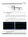
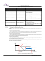
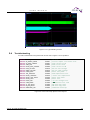
The following document contains information on Cypress products. Although the document is marked with the name “Spansion” and “Fujitsu”, the company that originally developed the specification, Cypress will continue to offer these products to new and existing customers. Continuity of Specifications There is no change to this document as a result of offering the device as a Cypress product. Any changes that have been made are the result of normal document improvements and are noted in the document history page, where supported. Future revisions will occur when appropriate, and changes will be noted in a document history page. Continuity of Ordering Part Numbers Cypress continues to support existing part numbers. To order these products, please use only the Ordering Part Numbers listed in this document. Worldwide Sales and Design Support We look forward to partnering with you to provide solutions that will help make your systems successful. Cypress maintains a worldwide network of offices, solution centers, manufacturer’s representatives, and distributors. To find the office closest to you, visit us at Cypress Locations. About Cypress Cypress (NASDAQ: CY) delivers high-performance, high-quality solutions at the heart of today’s most advanced embedded systems, from automotive, industrial and networking platforms to highly interactive consumer and mobile devices. With a broad, differentiated product portfolio that includes NOR flash ® memories, F-RAM™ and SRAM, Traveo™ microcontrollers, the industry’s only PSoC programmable ® system-on-chip solutions, analog and PMIC Power Management ICs, CapSense capacitive touch® sensing controllers, and Wireless BLE Bluetooth Low-Energy and USB connectivity solutions, Cypress is committed to providing its customers worldwide with consistent innovation, best-in-class support and exceptional system value. 3-Phase ACIM Scalar Control Slip Speed Control Solution 32-BIT MICROCONTROLLER FM0+ Family User Manual June 15, 2015, AN710-00009-1v0-E 1 U S E R M A N U A L Target products This application note is described about below products: Series S6E1A1 2 Product Number (not included Package suffix) All types AN710-00009-1v0-E, June 15, 2015 U S E R M A N U A L Table of Contents 1. Introduction .............................................................................................................................................. 6 1.1 Purpose .......................................................................................................................................... 6 1.2 Document Overview ....................................................................................................................... 6 2. System Hardware Environment .............................................................................................................. 7 3. Development Environment ..................................................................................................................... 8 4. Firmware Introduction ............................................................................................................................. 9 4.1 Firmware Features ......................................................................................................................... 9 4.2 Firmware Architecture .................................................................................................................... 9 4.2.1 Firmware Execution Flow .................................................................................................. 10 4.2.2 Files Description ................................................................................................................ 11 5. Getting Started ....................................................................................................................................... 14 5.1 Hardware Configuration ................................................................................................................ 14 5.2 Firmware Configuration ................................................................................................................ 15 5.2.1 Basic Drive Parameters..................................................................................................... 15 5.2.2 Motor Parameters.............................................................................................................. 15 5.2.3 Hall Sensor Parameters .................................................................................................... 15 5.2.4 Startup Parameters ........................................................................................................... 15 5.2.5 Normal Running Parameters ............................................................................................. 16 5.2.6 Braking Parameters........................................................................................................... 16 5.2.7 Field Weakening Parameters ............................................................................................ 16 5.2.8 PI Parameters ................................................................................................................... 17 5.2.9 Protection Parameters....................................................................................................... 17 5.3 Debug Slip Speed Control System ............................................................................................... 17 5.3.1 Check Your Hardware ....................................................................................................... 17 5.3.2 Startup Your Motor ............................................................................................................ 18 5.3.3 Tuning PI Parameters ....................................................................................................... 18 5.3.4 Tuning Slip Speed ............................................................................................................. 19 5.3.5 Tuning High Speed Region ............................................................................................... 19 5.3.6 Tuning the Braking Function ............................................................................................. 20 5.4 Troubleshooting ............................................................................................................................ 21 6. Reference Documents ........................................................................................................................... 22 7. Additional Information .......................................................................................................................... 23 June 15, 2015, AN710-00009-1v0-E 3 U S E R M A N U A L Figures Figure 4-1: Overview of Firmware File System........................................................................................... 9 Figure 4-2: Firmware Execution Flow ....................................................................................................... 10 Figure 4-3: Block Diagram of Slip Speed Control System ......................................................................... 11 Figure 4-4: Firmware Layers Introduction .................................................................................................. 11 Figure 5-1: Top View of Demo PCB .......................................................................................................... 14 Figure 5-2: Hardware Information Configuration ...................................................................................... 14 Figure 5-3: Live Watch of IAR System...................................................................................................... 17 Figure 5-4: Voltage PI Regulation Parameters ......................................................................................... 18 Figure 5-5: Auto-Tuning of Kp According to Target Speed........................................................................ 19 Figure 5-6: 580 RPM with Different Slip Speed ........................................................................................ 19 Figure 5-7: Command Voltage in Braking Process ................................................................................... 20 Figure 5-8: A Typical Braking Process ...................................................................................................... 21 Figure 5-9: Fault Code of Slip Speed Control System .............................................................................. 21 4 AN710-00009-1v0-E, June 15, 2015 U S E R M A N U A L Tables Table 2-1: Demo System Hardware Environment....................................................................................... 7 Table 3-1: Development Environment ........................................................................................................ 8 Table 4-1: Firmware Features .................................................................................................................... 9 Table 4-2: Source Files Description .......................................................................................................... 12 Table 5-1: High Speed Region Tuning Parameters .................................................................................. 20 June 15, 2015, AN710-00009-1v0-E 5 U S E R 1. M A N U A L Introduction 1.1 Purpose This user manual introduces scalar control of a 3-phase ACIM solution with slip speed control scheme. The slip speed control scheme is known as an easy constructed, high efficiency, and medium dynamic response control algorithm. In this document, the slip speed control is realized by capturing rotor speed by hall sensor to form speed close loop control. Further utilizing one channel ADC to sample DC bus voltage, SVPWM is generated. According to one PI regulator for voltage control, and one PI regulator for slip speed control, this scheme is realized for full speed range. To prevent abnormal operations, over/under voltage protection, hall lost/lock rotor protection, and motor lose phase protection are dedicatedly designed and implemented. 1.2 Document Overview The rest of this document is organized as below: Chapter 2 explains System Hardware Environment. Chapter 3 explains Development Environment. Chapter 4 explains Firmware Introduction. Chapter 5 explains Getting Started. Chapter 6 explains Reference Documents. 6 AN710-00009-1v0-E, June 15, 2015 U S E R 2. M A N U A L System Hardware Environment Table 2-1: Demo System Hardware Environment Name Type Description Remark 32-bit ARM Cortex-M0+ Core 32 Pins MCU Series S6E1A12B0AGP2 Maximum operating frequency: 40MHz On-chip flash memory: 88 Kbyte On-chip SRAM: 6 Kbyte Maximum carrier frequency: 20 kHz Maximum main supply voltage: 400 V IPM Module SCM1559M Maximum output current (continued): 10 A Logic supply voltage: 13.5~16.5 V Minimum dead time: 1.0 us June 15, 2015, AN710-00009-1v0-E 7 U S E R 3. M A N U A L Development Environment Table 3-1: Development Environment Name 8 Description Part Number Manufacturer Remark IAR Embedded Workbench 6.6 Code edit, compile, and online debug N/A N/A N/A Spansion Flash Loader Flash download program N/A N/A N/A J-Link IAR connection to target board N/A N/A N/A Eclipse Code edit N/A N/A N/A Windows 7 Enterprise Operation system (service pack 1, 64bit) N/A N/A N/A AN710-00009-1v0-E, June 15, 2015 U S E R 4. M A N U A L Firmware Introduction 4.1 Firmware Features Table 4-1: Firmware Features No. 4.2 Feature Description Remark Speed sensor is required. 1 Slip speed control ACIM is controlled with optimized efficiency with slip speed controller. 2 Braking function Braking down motor with no additional hardware. 3 Field weakening control Speed range of motor is extended by slip speed regulation. 4 Bi-direction rotation Both clockwise and counter-clockwise rotation are OK. 5 Over current protection Hardware over current protection. (Software protection is available if current sensor is implemented) 6 Voltage protection Irregular HIGH/LOW voltage protection, normal over/under voltage protection. 7 Hall lost/Lock rotor protection Prevent long time operation in no speed signal case. 8 Phase lose protection Motor phase lose case will be protected. 9 Variable carrier frequency Maximum 16kHz 10 UART communication UART communication with host machine 11 OOB function Out-of balance for washing machine application 12 Weighting function Weight measurement for washing machine application Firmware Architecture Figure 4-1: Overview of Firmware File System June 15, 2015, AN710-00009-1v0-E 9 U S E R 4.2.1 M A N U A L Firmware Execution Flow Figure 4-2 shows the execution flow of firmware that controls an ACIM by slip speed controller. In main function, after MCU and control system are initialized, a while loop is executed that starts/stops motor according to user command speed. In another hand, UART communication and timer event are processed for user defined operations. In normal control occasion, three main interrupt routines are executed. FRT zero interrupt occurs at a frequency named carries frequency, and once FRT interrupt happens, an ADC interrupt is triggered to sample DC bus voltage and current. After AD sample, motor control is executed in FRT interrupt routine, with the knowledge of sampled voltage and rotor speed. Another interrupt is triggered by Hall signal to capture rotor speed, and both the falling edge and rising edge are captured to calculate rotor speed. In abnormal ISR routines, a DTTI interrupt is triggered by a fault signal from IPM, and activates hardware over current protection and immediately stop the motor. The WDT (watch dog timer) interrupt is triggered by both hardware and software WDT, and once this interrupt is triggered, motor will be stopped immediately. Figure 4-3 shows the block diagram of slip speed control system. For more information of slip speed control, please refer to S6E1A1_AN710-00001-1v0-E-3Phase_ACIM_Scalar_Control.pdf. main function entrance Initialize MCU Initialize control Main Loop Abnormal ISR Routines Start/Stop motor control UART communication Timer event 1. Speed set 2. Protection 3. Parameter tuning DTTI ISR Stop motor WDT ISR Stop motor Normal ISR Routines Trig ADC sample BT ISR Rotor Speed calculate speed FRT ISR ADC ISR Return sample 1. Vbus Sample 2. Ibus Sample Motor Control 1. Voltage regulate 2. Slip regulate 3. Brake control 4. SVPWM Figure 4-2: Firmware Execution Flow 10 AN710-00009-1v0-E, June 15, 2015 U S E R M A N U A L 𝑉𝑞∗ = 0 𝜔𝑟∗ Inv. Park 𝑉𝑑∗ 𝜔𝑟 + PI PWM 𝜃𝑒 𝑀𝑎𝑥 𝑉𝑑∗ PI 𝜔𝑠∗ + 𝜔𝑠𝑠𝑒𝑡 1 𝑠 + enable/disable field weakening 𝜔𝑟 ACIM Figure 4-3: Block Diagram of Slip Speed Control System 4.2.2 Files Description User Layer User interface Main program entrance Interrupt vectors App Layer AcimSlipCtrl Brake HallSpeedDetect SpeedSet Protection A/D Sample InitMcu Isr OOB Weight Timer Event UART Crc Module Layer EquivalentTransformation Math Filter PI Regulator SVPWM Drive Layer Global Layer Figure 4-4: Firmware Layers Introduction June 15, 2015, AN710-00009-1v0-E 11 U S E R M A N U A L Table 4-2: Source Files Description Layer Files Description interrupts.c S01_global pdl.c MCU related files. system_s6e1a1.c adc.c bt.c hwwdg.c mft_adcmp.c S02_driver MCU drivers. mft_frt.c mft_ocu.c mft_wfg.c swwdg.c EquivalentTransformation.c Filter.c Math.c S03_module Basic functions for motor control. Pid.c PidReg_cm0_64bit.asm Scpwm_cm0.asm S04_app S05_user 12 AdcSample.c ADC sample parameter initialization and offset check. Brake.c Braking function of ACIM. crc.c crc check for UART communication HallSpeedDetect.c Hall speed detection called in BT ISR for speed measurement. InitMcu.c Initialize MCU peripherals. Isr.c ISR interrupt entrance. MotorCtrl.c Motor control files, including initialization, startup motor, stop motor, and FRT routine called by FRT ISR. OOB.c OOB function of washing machine. Protection.c Protection functions, including voltage protection, Hall lost/Lock rotor protection, and lose phase protection SpeedSet.c Command and target speed set functions. TimerEvent.c Timer triggered functions, including speed set, protection, and parameter self-adjustment. UART.c UART communication Weight.c Weight measure of washing machine Main.c main function startup_s6xxxx.s Vector table of target MCU. CustomerInterface.c Customer interface for parameter configuration. AN710-00009-1v0-E, June 15, 2015 U S E R M A N U A L The firmware consists with five layers, and each layer places header files and source files separately. Figure 4-4 shows the functions of each layer, and Table 4-2 describes the details. June 15, 2015, AN710-00009-1v0-E 13 U S E R 5. M A N U A L Getting Started 5.1 Hardware Configuration Motor Temperature Protection Port L N U V Hall Sensor W UART J-Link Figure 5-1: Top View of Demo PCB Figure 5-1 shows the top view of demo PCB. First connect motor cables and motor temperature protection port. If there is no temperature port, short this port. Insert J-Link wire, and connect AC cables. Now the PCB is ready for your debug. If your hardware is different from demo PCB, please configure your hardware infomation in H05_user\ HardwareConfig.c. For further information of your hardware, please find H04_user\InitMcu.c to adapt your hardware. #define #define #define #define ADC_VOLT_REF ADC_VALUE_MAX VDC_FACTOR ADC_CH_VDC #define ADC_CH_I_BUS #define ADC_I_BUS_FACTOR #define ADC_I_BUS_BIAS // configure hall I/O and Pin #define USER_BT_TIMER_SIZE #define HALL_A_TIMER_LOW_CH /** UART Select */ #define FM0P_MFSx_UART 5.0f 4096.0f 93.3 2 //reference voltage of ADC sample //4096 for 12bit ADC //gain of DC bus voltage samplling //ADC channel of DC bus voltage 1 15.6 2048 // ADC channel of DC bus current // gain of DC bus current sampling // bias of DC bus current sampling PwcSize16Bit; FM0P_BT0_PWC //base timer PWC size //base timer unit for hall speed FM0P_MFS3_UART //MFS unit for UART communication Figure 5-2: Hardware Information Configuration 14 AN710-00009-1v0-E, June 15, 2015 U S E R 5.2 M A N U A L Firmware Configuration Before startup your motor, please configure your control target to make sure motor is operated correctly. You can find firmware configuration parameters in S05_user\CustomerInterface.c. 5.2.1 Basic Drive Parameters // // carrier // uint16_t float32_t uint32_t frequency and dead time MotorCtrl_u16CarrierFreq MotorCtrl_f32DeadTimeUs RelayDelayOnTms = 16000; = 2.0f; = 2000; // carrier frequency (Hz) // Dead timer us // the time delay for relay switched //on,unit:ms First of all, select your carrier frequency and dead time for motor drive. Set a time delay for relay open when system power is on. 5.2.2 Motor Parameters // // motor parameters // int32_t MotorCtrl_i32PolePairs float32_t Motor_f32TransRate float32_t MotorCtrl_f32MaxVf int32_t MotorCtrl_i32RpmMin int32_t MotorCtrl_i32RpmMax 5.2.3 = = = = = 2; 11.6; 3.0; 30; 1200; // // // // // pole pairs TransRate of motor maximum V/f ratio minimum speed maximum speed Hall Sensor Parameters // // hall speed sensor // uint32_t MotorCtrl_u32EdgesPerCycle float32_t MotorCtrl_f32BaseTimerClkMHz = 16; // hall edges per motor cycle = 10.0; // Base timer clock In this firmware, motor speed is measured from a hall sensor, and captured by base timer. The base timer captures both the falling edge and rising edge of hall signal. For example: Your hall sensor returns 8 pulses per mechanical cycle, then you have 8 falling edges and 8 rising edges, therefore 16 edges per cycle is set. 5.2.4 Startup Parameters // // motor start-up settings // int32_t MotorCtrl_i32StartRpm1 int32_t MotorCtrl_i32StartRpm2 float32_t MotorCtrl_f32StartWsHz int32_t MotorCtrl_i32StartAccRpmPerSec June 15, 2015, AN710-00009-1v0-E = 100; = 400; = 8.0; = 1500; 15 U S E R M A N U A L The startup process applies slip speed curve for large startup torque. This section defines the transition point at startup as well as speed acceleration rate. 5.2.5 Normal Running Parameters // // motor normal running settings // float32_t MotorCtrl_f32MinWsHz float32_t MotorCtrl_f32MaxWsHz = 2.8; // (Hz) nominal slip speed = 18.0; // (Hz) maximum slip speed The normal running operation requires two slip speeds. One is for low speed and medium speed region that applies MTPA control, named as minimum slip speed. Another is for field weakening control, which defines the maximum slip speed allowed in field weakening region. 5.2.6 Braking Parameters // // motor brake settings // float32_t MotorCtrl_f32FreeBrakeVsRamp float32_t MotorCtrl_f32ForceBrakeVs float32_t MotorCtrl_f32ForceBrakeVsRamp = 25.0; = 19.0; = 200.0; // Volt/second // Volt // Volt/second The braking process has two steps. First when motor is under AC excitation, stator voltage will decrease to zero with voltage ramp defined by MotorCtrl_f32FreeBrakeVsRamp. If force brake is enabled in braking process, a DC voltage with amplitude MotorCtrl_f32ForceBrakeVs will be imposed on stator, and the rising ramp of this voltage is defined by MotorCtrl_f32ForceBrakeVsRamp. 5.2.7 Field Weakening Parameters // // field weakening control // float32_t MotorCtrl_f32FwUpperVsK float32_t MotorCtrl_f32FwLowerVsK = 0.97; = 0.91; Two voltage ratio of maximum output voltage is defined for field weakening control, 0.90~0.99 are recommended for these two values. 16 AN710-00009-1v0-E, June 15, 2015 U S E R 5.2.8 M A N U A L PI Parameters // // PI parameters // float32_t MotorCtrl_f32SpdRegTimeMs // voltage PI regulator int32_t MotorCtrl_i32LowSpdRpm int32_t MotorCtrl_i32HighSpdRpm float32_t MotorCtrl_f32LowSpdVsKp float32_t MotorCtrl_f32LowSpdVsKi = = = = float32_t float32_t = 0.5; // high speed Kp of voltage PI = 1.0; // high speed Kp of voltage PI MotorCtrl_f32HighSpdVsKp MotorCtrl_f32HighSpdVsKi // slip speed PI regulator float32_t MotorCtrl_f32WsKp float32_t MotorCtrl_f32WsKi 5.2.9 = 0.6; // speed regulation cycle (ms) 1600; // low speed transition speed 3000; // high speed transition speed 2.5; // low speed Kp of voltage PI 6; // low speed Ki of voltage PI = 0; = 1; // Kp of slip speed PI for field weaken // Ki of slip speed PI for field weaken Protection Parameters // // protections // int32_t int32_t MotorCtrl_i32OverVoltage MotorCtrl_i32UnderVoltage = 360; = 200; int32_t int32_t MotorCtrl_i32IrreHighVoltage = 390; MotorCtrl_i32IrreLowVoltage = 100; // over voltage threshold // under voltage threshold // irregular high voltage limit // irregular low voltage limit In this firmware, over current protection is done by hardware, thus you only need to configure voltage protection in customer interface. There are two limits for both over voltage and under voltage protection. The irregular high voltage and irregular low voltage take a shorter time to trigger a protection than normal over voltage and under voltage. 5.3 Debug Slip Speed Control System 5.3.1 Check Your Hardware 4 5 3 2 1 Figure 5-3: Live Watch of IAR System June 15, 2015, AN710-00009-1v0-E 17 U S E R M A N U A L After first time burning the firmware into hardware, check below items to make sure both your hardware and firmware are correctly configured: 1. Check item 1 in Figure 5-3. If fault code is 0x0000, no error code is detected. Otherwise refer to 5.4 to fix the problem. 2. Check item 2 in Figure 5-3. This item is DC bus voltage. If this value is in your expectation, then DC bus sample is OK. Otherwise check your ADC configuration and sample parameters. 3. Check item 3 in Figure 5-3.This item is rotor speed measured by Base Timer. In standstill case, this value should be zero. Rotate your motor, and keep watching this value, it becomes a non-zero integer when motor is rotating. If this value keeps being zero, check your Hall sensor and Base Timer configuration. 5.3.2 Startup Your Motor Once the hardware and firmware are properly configured, you are ready to rotate your motor. Input a speed into item 4 in Figure 5-3, this is command speed. At first time, run the motor in low speed region, and check whether the parameters are proper for your motor. You might confront below problems: 1. Fault Code: 0x0008 This means hardware over current protection is triggered. This is probably due to that a large V/f ratio caused over current protection; you can smaller the maximum V/f ratio as 5.2.2 described. Otherwise, check your hardware that whether you have set a too low value to hardware over current protection. 2. Fault Code: 0x0400 This is lock rotor protection or hall lost protection. Double confirm motor can be freely rotates, and hall sensor are correctly configured. Otherwise, refer to next problem. 3. Motor does not rotate with non-zero command speed If current appears but motor never rotates. This is probably that the maximum V/f ratio is too small to startup the motor; you can enlarge the maximum V/f ratio as 5.2.2 described. 5.3.3 Tuning PI Parameters Find the PI parameter for voltage regulation as Figure 5-4 shows. Tune the PI parameters such that both the dynamics and stability satisfies your requirement. Figure 5-5 shows the auto tuning process of Kp according to target speed, and Ki shares the same adjustment pattern. Figure 5-4: Voltage PI Regulation Parameters 18 AN710-00009-1v0-E, June 15, 2015 U S E R M A N U A L i32Q15_Kp i32Q15_LowSpdKp i32Q15_HighSpdKp TgtRPM i32LowSpdRpm i32HighSpdRpm Figure 5-5: Auto-Tuning of Kp According to Target Speed 5.3.4 Tuning Slip Speed The slip speed is the key factor to optimized power consumption operation. The theoretical optimal slip speed is calculated as 𝜔𝑠 = 𝑅𝑟 𝐿𝑟 This means that the optimal slip speed equals to the inverse of rotor time constant. Now drive the motor in a proper speed stably (no disturbance is preferred). Be aware that speed should not be too slow (or efficiency is quite low) or too high (otherwise field weakening is introduced). Find the minimum slip speed in live watch window Tune the parameter and observe phase current or input power. The optimized slips speed is found when minimum current or power is achieved. Record this slip speed and use this slip speed for your further application. Figure 5-6 shows the current waveform of motor at 580 RPM with different slip speed. Apparently, the target motor runs under slip speed equals to 2.8Hz approached a better efficiency. a. 𝜔𝑠 = 5.0 Hz b. 𝜔𝑠 = 2.8 Hz Figure 5-6: 580 RPM with Different Slip Speed 5.3.5 Tuning High Speed Region The high speed region involves field weakening control. Due to the lack of current close-loop control, you are going to tuning below parameters to achieve a proper performance. Table 5-1 shows each parameter that relates to field weakening control. June 15, 2015, AN710-00009-1v0-E 19 U S E R M A N U A L Table 5-1: High Speed Region Tuning Parameters Parameter Customer Interface Variable Description Slip_stcWsPid.i32Q15_Kp MotorCtrl_f32WsKp Kp of slip speed PI regulator Slip_stcWsPid.i32Q15_Ki MotorCtrl_f32WsKi Ki of slip speed PI regulator MotorCtrl_f32FwLowerVsK Lower voltage threshold for field weakening control. Tuning target: Slip_stcSlipCtrl.i32Q8_LowerVsK 1. Field weakening is fluent and stably exited. Upper voltage threshold for field weakening control. Tuning target: Slip_stcSlipCtrl.i32Q8_UpperVsK MotorCtrl_f32FwUpperVsK 1. Field weakening enters fluently 2. Field weakening is effectively extending speed range. Maximum allowed slip speed for field weakening control. Tuning target:: Slip_stcSlipCtrl.i32Q8_MaxWsHz MotorCtrl_f32MaxWsHz 1. Speed range is extended 2. Current range is within rated value with slip speed equals to this value. 5.3.6 Tuning the Braking Function Figure 5-7 shows the command voltage in braking process. Three parameters are to be tuned for this function. 1. MotorCtrl_f32FreeBrakeVsRamp This is a voltage ramp in unit V/s that decreases the amplitude of AC voltage. Tune this ramp such that the DC bus voltage does not boost too much and the decreasing process as short as possible. 2. MotorCtrl_f32ForceBrakeVsRamp This is a voltage ramp in unit V/s that increases a DC voltage imposed to stator. Choose a proper one that current reaches to its stable point quickly with small overshoot. 3. MotorCtrl_f32ForceBrakeVs This is the braking DC voltage imposed on stator. Choose a proper voltage that rotor brakes fast and current amplitude is within the rated range is OK. Figure 5-8 shows a typical braking process with force braking. Channel 2 is stator current, channel 3 is DC bus voltage, and channel 4 is hall signal. 𝑉𝑠 MotorCtrl_f32FreeBrakeVsRamp MotorCtrl_f32ForceBrakeVsRamp MotorCtrl_f32ForceBrakeVs t start brake 𝜔𝑟 = 𝑇𝑎𝑟𝑔𝑒𝑡 𝜔𝑟 Figure 5-7: Command Voltage in Braking Process 20 AN710-00009-1v0-E, June 15, 2015 U S E R M A N U A L Figure 5-8: A Typical Braking Process 5.4 Troubleshooting For other unstated fault case, please refer to fault code in Figure 5-9 to fix problems. #define #define #define #define #define #define #define #define #define #define #define #define #define #define #define #define #define NORMAL_RUNNING AD_MIDDLE_ERROR SW_OVER_CURRENT SINK_ERR MOTOR_OVER_CURRENT OVER_VOLTAGE UNDER_VOLTAGE POWER_OVER IPM_TEMPOVER MOTOR_TEMPOVER MOTOR_LOSE_PHASE MOTOR_LOCK DCBUS_ERR COMM_ERROR SF_WTD_RESET HW_WTD_RESET UNDEFINED_INT 0x0000 0x0001 0x0002 0x0004 0x0008 0x0010 0x0020 0x0040 0x0080 0x0100 0x0200 0x0400 0x0800 0x1000 0x2000 0x4000 0x8000 //no error //current sample 2.5V offset error //over-current of FW //IPM circuit fault //over-current of HW //DC bus over-voltage //DC bus under-voltage //motor over-power //IPM temperature error // motor over temperature //motor lose phase //motor lock // dc bus voltage error //communicate error code //FW watch dog reset //HW watch dog reset //undefined interrupt Figure 5-9: Fault Code of Slip Speed Control System June 15, 2015, AN710-00009-1v0-E 21 U S E R 6. M A N U A L Reference Documents [1]. FM0+ S6E1A1 Series Data Sheet, Revision 0.1, 2013 [2]. FM0+ Family Peripheral Manual, Revision 1.0, 2014 [3]. FM0+ Family Timer Part Peripheral Manual, Revision 1.0, 2014 [4]. FM0+ Family Analog Macro Part Peripheral Manual, Revision 1.0, 2014 [5]. P. C. Krause, O. Wasynczuk, and S. D. Sudhoff, Electric Machinery and Drive Systems. IEEE Press, 2002 22 AN710-00009-1v0-E, June 15, 2015 U S E R 7. M A N U A L Additional Information For more Information on Spansion semiconductor products, visit the following websites: English version address: http://www.spansion.com/Products/microcontrollers/ Chinese version address: http://www.spansion.com/CN/Products/microcontrollers/ Please contact your local support team for any technical question America: [email protected] China: [email protected] Europe: [email protected] Japan: [email protected] Other: http://www.spansion.com/Support/SES/Pages/Ask-Spansion.aspx June 15, 2015, AN710-00009-1v0-E 23 U S E R M A N U A L AN710-00009-1v0-E Spansion Controller Manual FM0+ Family 32-BIT MICROCONTROLLER S6E1A1 Series 3-Phase ACIM Scalar Control User Manual June 15 2015 Rev. 1.0 Published: Edited: 24 Spansion Inc. Embedded System Platform AN710-00009-1v0-E, June 15, 2015 U S E R M A N U A L Colophon The products described in this document are designed, developed and manufactured as contemplated for general use, including without limitation, ordinary industrial use, general office use, personal use, and household use, but are not designed, developed and manufactured as contemplated (1) for any use that includes fatal risks or dangers that, unless extremely high safety is secured, could have a serious effect to the public, and could lead directly to death, personal injury, severe physical damage or other loss (i.e., nuclear reaction control in nuclear facility, aircraft flight control, air traffic control, mass transport control, medical life support system, missile launch control in weapon system), or (2) for any use where chance of failure is intolerable (i.e., submersible repeater and artificial satellite). Please note that Spansion will not be liable to you and/or any third party for any claims or damages arising in connection with above-mentioned uses of the products. Any semiconductor devices have an inherent chance of failure. You must protect against injury, damage or loss from such failures by incorporating safety design measures into your facility and equipment such as redundancy, fire protection, and prevention of over-current levels and other abnormal operating conditions. If any products described in this document represent goods or technologies subject to certain restrictions on export under the Foreign Exchange and Foreign Trade Law of Japan, the US Export Administration Regulations or the applicable laws of any other country, the prior authorization by the respective government entity will be required for export of those products. Trademarks and Notice The contents of this document are subject to change without notice. This document may contain information on a Spansion product under development by Spansion. Spansion reserves the right to change or discontinue work on any product without notice. The information in this document is provided as is without warranty or guarantee of any kind as to its accuracy, completeness, operability, fitness for particular purpose, merchantability, non-infringement of third-party rights, or any other warranty, express, implied, or statutory. Spansion assumes no liability for any damages of any kind arising out of the use of the information in this document. ® ® ® TM Copyright © 2015 Spansion All rights reserved. Spansion , the Spansion logo, MirrorBit , MirrorBit Eclipse , TM TM TM ORNAND , Easy DesignSim , Traveo and combinations thereof, are trademarks and registered trademarks of Spansion LLC in the United States and other countries. Other names used are for informational purposes only and may be trademarks of their respective owners. June 15, 2015, AN710-00009-1v0-E 25