1
21-32-6100-0598
USER'S MANUAL
KS32C6100
32-Bit RISC
Microcontroller
Revision 1
Important Notice
The information in this publication has been carefully
checked and is believed to be accurate at the time of
publication. Samsung assumes no responsibility,
however, for possible errors or omissions, or for any
consequences resulting from the use of the
information contained herein.
Samsung reserves the right to make changes to its
products or product specifications with the intent to
improve function or design at any time and without
notice and is not required to update this
documentation to reflect such changes.
This publication does not convey to a purchaser of
semiconductor devices described herein any license
under the patent rights of Samsung or others.
Samsung makes no warranty, representation, or
guarantee regarding the suitability of its products for
any particular purpose, nor does Samsung assume
any liability arising out of the application or use of any
product or circuit and specifically disclaims any and all
liability, including without limitation any consequential
or incidental damages.
"Typical" parameters can and do vary in different
applications. All operating parameters, including
"Typicals," must be validates for each customer
application by the customer’s technical experts.
Samsung products are not designed, intended, or
authorized for use as components in systems intended
for surgical implant into the body, for other applications
intended to support or sustain life, or for any other
application in which the failure of the Samsung product
could create a situation where personal injury or death
may occur.
Should the Buyer purchase or use a Samsung product
for any such unintended or unauthorized application,
the Buyer shall indemnify and hold Samsung and its
officers, employees, subsidiaries, affiliates, and
distributors harmless against all claims, costs,
damages, expenses, and reasonable attorney fees
arising out of, either directly or indirectly, any claim of
personal injury of death that may be associated with
such unintended or unauthorized use, even if such
claim alleges that Samsung was negligent regarding
the design or manufacture of said product.
KS32C6100 32-Bit RISC Microcontroller User’s Manual
Publication Number: 22-32-6100
Publication Date: March 1998
1998 Samsung Electronics
All rights reserved. No part of this publication may be reproduced, stored in a retrieval system, or transmitted in any form orby
any means, electric or mechanical, by photocopying, recording, or otherwise, without the prior written consent of Samsung
Electronics.
Samsung Electronic’s microcontroller business has been awarded full ISO-14001
certification (BVQI Certificate No. 9330). All semiconductor products are designed and
manufactured in accordance with the highest quality standards and objectives.
Samsung Electronics Co., Ltd.
San #24, Nongseo-Ri, Kiheung-Eup
Yongin-City, Kyungi-Do, Korea
C.P.O. Box #37, Suwon 449-900
Phone: (02) 760-6530, (0331) 209-6530
Fax:
(02) 760-6547
Internet: http://www.samsungsemi.com
Printed in the Republic of Korea
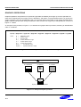
Preface
The KS32C6100 Microcontroller User’s Manual is written for application designers who are using Samsung’s
KS32C6100 32-bit RISC microcontroller for application development. It has fourteen sections:
•
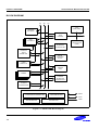
Section 1, "Product Overview," is a high-level introduction to the KS32C6100 and includes a features list, block
diagram, pin assignments, signal descriptions, a description of the CPU core, and an overview of special
registers.
•
Section 2, "Programmer’s Model," describes the important features of the KS32C6100 programming
environment.
•
Section 3, "Instruction Set," describes the features of the KS32C6100 instruction set, which is based on a CPU
core developed by ARM, Ltd.
•
Section 4, "System Manager," describes the System Manager function block which consists of registers that
control bus arbitration and management, as well as external memory access and timing.
•
Section 5, "Instruction/Data Cache," describes the 4-Kbyte unified cache and its control registers.
•
Section 6, "DMA Controller," describes the KS32C6100 direct memory access (DMA) controller, including DMA
operations, transfer modes, and CDMA/GDMA special registers.
•
Section 7, "UART/Serial I/O," describes the UART and SIO function blocks, including UART/SIO operations,
special registers, and timing.
•
Section 8, "Parallel Port," describes the parallel port interface controller (PPIC) function block, including various
operating modes and digital filtering, and the parallel port data, status, and control registers.
•
Section 9, "Programmable Timers," describes the five 16-bit timers, including tone generator and watchdog
functions, output modes, and special registers.
•
Section 10, "Printer Interface," describes the KS32C6100 printer interface controller (PIFC) function block,
including message communication, the video data controller, and PIFC special registers.
•
Section 11, "Graphic Engine Unit," describes the KS32C6100 graphic engine unit (GEU) which controls graphic
operations in the print engine. The description includes information about bit block transfers, scanline transfers,
as well as GEU special registers and register configuration.
•
Section 12, "Imaging Function Block," describes the image rotator and expander functions, variable image
scaling (VIS), halftoning operations, and related special registers.
•
Section 13, "I/O Ports," describes the KS32C6100 input/output ports and special registers, and includes I/O
timing information.
•
Section 14, "Interrupt Controller," describes the interrupt controller function block, including interrupt sources
and related special registers.
The remaining sections of this manual— Sections 15, 16, and 17— present D.C. and A.C. electrical data and related
timing diagrams, mechanical data for 208-pin QFP package, and an overview of available evaluation board
For additional information about the KS32C6100 parallel port interface controller, we recommend that you also
read the IEEE 1284 Parallel Port Standard. You can access a detailed technical introduction to this standard over
the Internet at http://www.fapo.com/ieee1284.htm.
KS32C6100 RISC MICROCONTROLLER
v
Table of Contents
1
Product Overview
Features . . . . . . . . . . . . . . . . . . . . . . . . . . . . . . . . . . . . . . . . . . . . . . . . . . . . . . . . . . . . .1-2
Block Diagram . . . . . . . . . . . . . . . . . . . . . . . . . . . . . . . . . . . . . . . . . . . . . . . . . . . . . . . . 1-4
Pin Assignments . . . . . . . . . . . . . . . . . . . . . . . . . . . . . . . . . . . . . . . . . . . . . . . . . . . . . . . 1-5
Signal Descriptions . . . . . . . . . . . . . . . . . . . . . . . . . . . . . . . . . . . . . . . . . . . . . . . . . . . . . 1-6
CPU Core . . . . . . . . . . . . . . . . . . . . . . . . . . . . . . . . . . . . . . . . . . . . . . . . . . . . . . . . . . . . 1-12
Instruction Set . . . . . . . . . . . . . . . . . . . . . . . . . . . . . . . . . . . . . . . . . . . . . . . . . . . . . . . . . 1-13
Memory Interface . . . . . . . . . . . . . . . . . . . . . . . . . . . . . . . . . . . . . . . . . . . . . . . . . . . . . . 1-14
Operating States . . . . . . . . . . . . . . . . . . . . . . . . . . . . . . . . . . . . . . . . . . . . . . . . . . . . . . . 1-14
Operating Modes . . . . . . . . . . . . . . . . . . . . . . . . . . . . . . . . . . . . . . . . . . . . . . . . . . . . . . . 1-14
Special Registers . . . . . . . . . . . . . . . . . . . . . . . . . . . . . . . . . . . . . . . . . . . . . . . . . . . . . .1-15
2
Programming Model
Processor Operating States . . . . . . . . . . . . . . . . . . . . . . . . . . . . . . . . . . . . . . . . . . . . . . 2-1
Conditions for Entering THUMB State . . . . . . . . . . . . . . . . . . . . . . . . . . . . . . . . . . . . . . . 2-1
Conditions for Entering ARM State . . . . . . . . . . . . . . . . . . . . . . . . . . . . . . . . . . . . . . . . .2-1
Memory Formats . . . . . . . . . . . . . . . . . . . . . . . . . . . . . . . . . . . . . . . . . . . . . . . . . . . . . . . 2-2
Big-Endian Format . . . . . . . . . . . . . . . . . . . . . . . . . . . . . . . . . . . . . . . . . . . . . . . . . . . . . 2-2
Little-Endian Format . . . . . . . . . . . . . . . . . . . . . . . . . . . . . . . . . . . . . . . . . . . . . . . . . . . . 2-2
Instruction Length . . . . . . . . . . . . . . . . . . . . . . . . . . . . . . . . . . . . . . . . . . . . . . . . . . . . . . 2-3
Data Types . . . . . . . . . . . . . . . . . . . . . . . . . . . . . . . . . . . . . . . . . . . . . . . . . . . . . . . . . . . 2-3
Operating Modes . . . . . . . . . . . . . . . . . . . . . . . . . . . . . . . . . . . . . . . . . . . . . . . . . . . . . . . 2-3
Registers . . . . . . . . . . . . . . . . . . . . . . . . . . . . . . . . . . . . . . . . . . . . . . . . . . . . . . . . . . . . . 2-4
ARM State Register Set . . . . . . . . . . . . . . . . . . . . . . . . . . . . . . . . . . . . . . . . . . . . . . . . . 2-4
ARM State Registers R14–R16 . . . . . . . . . . . . . . . . . . . . . . . . . . . . . . . . . . . . . . . . . . . . 2-4
Register Mapping in FIQ Mode . . . . . . . . . . . . . . . . . . . . . . . . . . . . . . . . . . . . . . . . . . . . 2-4
THUMB State Register Set . . . . . . . . . . . . . . . . . . . . . . . . . . . . . . . . . . . . . . . . . . . . . . . 2-6
Relationships Between ARM and THUMB State Registers . . . . . . . . . . . . . . . . . . . . . . 2-7
Accessing Hi-Registers in THUMB State . . . . . . . . . . . . . . . . . . . . . . . . . . . . . . . . . . . . 2-8
Program Status Registers . . . . . . . . . . . . . . . . . . . . . . . . . . . . . . . . . . . . . . . . . . . . . . . . 2-8
Exceptions . . . . . . . . . . . . . . . . . . . . . . . . . . . . . . . . . . . . . . . . . . . . . . . . . . . . . . . . . . . . 2-11
Entering Exception Processing . . . . . . . . . . . . . . . . . . . . . . . . . . . . . . . . . . . . . . . . . . . . 2-11
Exiting Exception Processing . . . . . . . . . . . . . . . . . . . . . . . . . . . . . . . . . . . . . . . . . . . . . 2-11
Summary of Exception Entry and Exit . . . . . . . . . . . . . . . . . . . . . . . . . . . . . . . . . . . . . . . 2-12
Fast Interrupt Requests (FIQ) . . . . . . . . . . . . . . . . . . . . . . . . . . . . . . . . . . . . . . . . . . . . . 2-12
Interrupt Requests (IRQ) . . . . . . . . . . . . . . . . . . . . . . . . . . . . . . . . . . . . . . . . . . . . . . . . . 2-13
Aborts . . . . . . . . . . . . . . . . . . . . . . . . . . . . . . . . . . . . . . . . . . . . . . . . . . . . . . . . . . . . . . . 2-13
Software Interrupts (SWI) . . . . . . . . . . . . . . . . . . . . . . . . . . . . . . . . . . . . . . . . . . . . . . . . 2-14
Undefined Instruction Trap . . . . . . . . . . . . . . . . . . . . . . . . . . . . . . . . . . . . . . . . . . . . . . . 2-14
Exception Vectors . . . . . . . . . . . . . . . . . . . . . . . . . . . . . . . . . . . . . . . . . . . . . . . . . . . . . .2-14
Exception Priorities . . . . . . . . . . . . . . . . . . . . . . . . . . . . . . . . . . . . . . . . . . . . . . . . . . . . . 2-15
vii
Table of Contents
Handling Contention During Exception Processing . . . . . . . . . . . . . . . . . . . . . . . . . . . . .2-15
Interrupt Latencies . . . . . . . . . . . . . . . . . . . . . . . . . . . . . . . . . . . . . . . . . . . . . . . . . . . . . .2-15
nRESET . . . . . . . . . . . . . . . . . . . . . . . . . . . . . . . . . . . . . . . . . . . . . . . . . . . . . . . . . . . . . .2-16
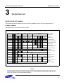
3
Instruction Set
ARM Instruction Set Formats . . . . . . . . . . . . . . . . . . . . . . . . . . . . . . . . . . . . . . . . . . . . .3-1
ARM Instruction Set Summary . . . . . . . . . . . . . . . . . . . . . . . . . . . . . . . . . . . . . . . . . . . .3-2
The Condition Field . . . . . . . . . . . . . . . . . . . . . . . . . . . . . . . . . . . . . . . . . . . . . . . . . . . . .3-3
Branch and Exchange (BX) . . . . . . . . . . . . . . . . . . . . . . . . . . . . . . . . . . . . . . . . . . . . . . .3-4
Branch, Branch with Link (B, BL) . . . . . . . . . . . . . . . . . . . . . . . . . . . . . . . . . . . . . . . . . . .3-6
Data Processing Instructions . . . . . . . . . . . . . . . . . . . . . . . . . . . . . . . . . . . . . . . . . . . . . .3-8
PSR Transfers (MRS, MSR) . . . . . . . . . . . . . . . . . . . . . . . . . . . . . . . . . . . . . . . . . . . . . .3-19
Multiply, Multiply-Accumulate (MUL, MLA) . . . . . . . . . . . . . . . . . . . . . . . . . . . . . . . . . . .3-23
Multiply Long and Multiply-Accumulate Long (MULL,MLAL) . . . . . . . . . . . . . . . . . . . . . .3-26
Single Data Transfer (LDR, STR) . . . . . . . . . . . . . . . . . . . . . . . . . . . . . . . . . . . . . . . . . .3-29
Half-Word and Signed Data Transfer (LDRH/STRH/LDRSB/LDRSH) . . . . . . . . . . . . . .3-35
Block Data Transfers (LDM, STM) . . . . . . . . . . . . . . . . . . . . . . . . . . . . . . . . . . . . . . . . .3-42
Single Data Swap (SWP) . . . . . . . . . . . . . . . . . . . . . . . . . . . . . . . . . . . . . . . . . . . . . . . .3-49
Software Interrupt (SWI) . . . . . . . . . . . . . . . . . . . . . . . . . . . . . . . . . . . . . . . . . . . . . . . . .3-51
Coprocessor Data Operation (CDP) . . . . . . . . . . . . . . . . . . . . . . . . . . . . . . . . . . . . . . . .3-53
Coprocessor Data Transfer (LDC, STC) . . . . . . . . . . . . . . . . . . . . . . . . . . . . . . . . . . . . .3-55
Coprocessor Register Transfers (MRC, MCR) . . . . . . . . . . . . . . . . . . . . . . . . . . . . . . . .3-58
Undefined Instruction . . . . . . . . . . . . . . . . . . . . . . . . . . . . . . . . . . . . . . . . . . . . . . . . . . . .3-61
ARM Instruction Set Examples . . . . . . . . . . . . . . . . . . . . . . . . . . . . . . . . . . . . . . . . . . . .3-62
Using Conditionals for Logical OR . . . . . . . . . . . . . . . . . . . . . . . . . . . . . . . . . . . . . . . . . .3-62
Absolute Value . . . . . . . . . . . . . . . . . . . . . . . . . . . . . . . . . . . . . . . . . . . . . . . . . . . . . . . .3-62
Run-Time Multiplication by 4, 5, or 6 . . . . . . . . . . . . . . . . . . . . . . . . . . . . . . . . . . . . . . . .3-62
Combining Discrete Tests and Range Tests . . . . . . . . . . . . . . . . . . . . . . . . . . . . . . . . . .3-62
Division and Remainder Routines . . . . . . . . . . . . . . . . . . . . . . . . . . . . . . . . . . . . . . . . . .3-63
Overflow Detection in the ARM7TDMI Core . . . . . . . . . . . . . . . . . . . . . . . . . . . . . . . . . .3-64
Pseudo-Random Binary Sequence Generator . . . . . . . . . . . . . . . . . . . . . . . . . . . . . . . .3-65
Using the Barrel Shifter to Multiply by a Constant . . . . . . . . . . . . . . . . . . . . . . . . . . . . . .3-65
Loading a Word from an Unknown Alignment . . . . . . . . . . . . . . . . . . . . . . . . . . . . . . . . .3-67
THUMB Instruction Set . . . . . . . . . . . . . . . . . . . . . . . . . . . . . . . . . . . . . . . . . . . . . . . . . .3-68
THUMB Instruction Formats . . . . . . . . . . . . . . . . . . . . . . . . . . . . . . . . . . . . . . . . . . . . . .3-68
THUMB Instruction Set Summary . . . . . . . . . . . . . . . . . . . . . . . . . . . . . . . . . . . . . . . . . .3-69
Format 1: Move Shifted Register . . . . . . . . . . . . . . . . . . . . . . . . . . . . . . . . . . . . . . . . . . .3-71
Format 2: Add/Subtract . . . . . . . . . . . . . . . . . . . . . . . . . . . . . . . . . . . . . . . . . . . . . . . . . .3-73
Format 3: Move/Compare/Add/Subtract Immediate . . . . . . . . . . . . . . . . . . . . . . . . . . . .3-75
Format 4: ALU Operations . . . . . . . . . . . . . . . . . . . . . . . . . . . . . . . . . . . . . . . . . . . . . . . .3-77
Format 5: Hi-Register Operations/Branch Exchange . . . . . . . . . . . . . . . . . . . . . . . . . . .3-79
Format 6: PC-Relative Load . . . . . . . . . . . . . . . . . . . . . . . . . . . . . . . . . . . . . . . . . . . . . .3-82
viii
Table of Contents
Format 7: Load/Store With Register Offset . . . . . . . . . . . . . . . . . . . . . . . . . . . . . . . . . . . 3-83
Format 8: Load/Store Sign-Extended Byte/Half-Word . . . . . . . . . . . . . . . . . . . . . . . . . . 3-85
Format 9: Load/Store With Immediate Offset . . . . . . . . . . . . . . . . . . . . . . . . . . . . . . . . . 3-87
Format 10: Load/Store Half-Word . . . . . . . . . . . . . . . . . . . . . . . . . . . . . . . . . . . . . . . . . . 3-89
Format 11: SP-Relative Load/Store . . . . . . . . . . . . . . . . . . . . . . . . . . . . . . . . . . . . . . . . 3-91
Format 12: Load Address . . . . . . . . . . . . . . . . . . . . . . . . . . . . . . . . . . . . . . . . . . . . . . . . 3-93
Format 13: Add Offset to Stack Pointer . . . . . . . . . . . . . . . . . . . . . . . . . . . . . . . . . . . . . . 3-95
Format 14: Push/Pop Registers . . . . . . . . . . . . . . . . . . . . . . . . . . . . . . . . . . . . . . . . . . . 3-97
Format 15: Multiple Load/Store . . . . . . . . . . . . . . . . . . . . . . . . . . . . . . . . . . . . . . . . . . . . 3-99
Format 16: Conditional Branch . . . . . . . . . . . . . . . . . . . . . . . . . . . . . . . . . . . . . . . . . . . . 3-101
Format 17: Software Interrupt . . . . . . . . . . . . . . . . . . . . . . . . . . . . . . . . . . . . . . . . . . . . . 3-103
Format 18: Unconditional Branch . . . . . . . . . . . . . . . . . . . . . . . . . . . . . . . . . . . . . . . . . . 3-105
Format 19: Long Branch With Link . . . . . . . . . . . . . . . . . . . . . . . . . . . . . . . . . . . . . . . . . 3-106
THUMB Instruction Set Examples . . . . . . . . . . . . . . . . . . . . . . . . . . . . . . . . . . . . . . . . . . 3-108
Using Shifts and Adds to Multiply by a Constant . . . . . . . . . . . . . . . . . . . . . . . . . . . . . . . 3-108
General-Purpose Signed Division . . . . . . . . . . . . . . . . . . . . . . . . . . . . . . . . . . . . . . . . . . 3-109
Division by a Constant . . . . . . . . . . . . . . . . . . . . . . . . . . . . . . . . . . . . . . . . . . . . . . . . . . . 3-111
4
System Manager
System Manager Registers . . . . . . . . . . . . . . . . . . . . . . . . . . . . . . . . . . . . . . . . . . . . . . . 4-3
System configuration Register . . . . . . . . . . . . . . . . . . . . . . . . . . . . . . . . . . . . . . . . . . . . 4-3
ROM Timing Control Register . . . . . . . . . . . . . . . . . . . . . . . . . . . . . . . . . . . . . . . . . . . . . 4-4
SRAM Timing Control Register . . . . . . . . . . . . . . . . . . . . . . . . . . . . . . . . . . . . . . . . . . . . 4-5
DRAM Timing Control Registers . . . . . . . . . . . . . . . . . . . . . . . . . . . . . . . . . . . . . . . . . . . 4-6
External I/O Access Timing Control Registers . . . . . . . . . . . . . . . . . . . . . . . . . . . . . . . . 4-7
Data Bus Width Control Registers . . . . . . . . . . . . . . . . . . . . . . . . . . . . . . . . . . . . . . . . . . 4-8
Memory Bank Address Pointer Registers . . . . . . . . . . . . . . . . . . . . . . . . . . . . . . . . . . . . 4-9
DRAM Refresh Control Register . . . . . . . . . . . . . . . . . . . . . . . . . . . . . . . . . . . . . . . . . . . 4-10
DRAM Self-Refresh Mode . . . . . . . . . . . . . . . . . . . . . . . . . . . . . . . . . . . . . . . . . . . . . . . . 4-13
Self-Refresh Mode Initiated by Hardware . . . . . . . . . . . . . . . . . . . . . . . . . . . . . . . . . . . . 4-13
Self-Refresh Mode Initiated by Software . . . . . . . . . . . . . . . . . . . . . . . . . . . . . . . . . . . . . 4-15
Memory Banks allocation . . . . . . . . . . . . . . . . . . . . . . . . . . . . . . . . . . . . . . . . . . . . . . . . 4-16
Base Pointer and Next Pointer Values . . . . . . . . . . . . . . . . . . . . . . . . . . . . . . . . . . . . . . 4-16
An Exception For Next Pointer Definition . . . . . . . . . . . . . . . . . . . . . . . . . . . . . . . . . . . . 4-16
Avoiding Memory Bank Overlap During Bank Pointer Updates . . . . . . . . . . . . . . . . . . . 4-16
Memory Map Definition at System Start-up . . . . . . . . . . . . . . . . . . . . . . . . . . . . . . . . . . . 4-17
Example of Mapping External Memory Banks . . . . . . . . . . . . . . . . . . . . . . . . . . . . . . . . 4-18
Mapping System Address Space to External Memory . . . . . . . . . . . . . . . . . . . . . . . . . . 4-21
Data bus connection with External Memory . . . . . . . . . . . . . . . . . . . . . . . . . . . . . . . . . . 4-21
System Bus Arbitration . . . . . . . . . . . . . . . . . . . . . . . . . . . . . . . . . . . . . . . . . . . . . . . . . . 4-23
External Bus Mastership . . . . . . . . . . . . . . . . . . . . . . . . . . . . . . . . . . . . . . . . . . . . . . . . . 4-24
Handshaking Protocol Description . . . . . . . . . . . . . . . . . . . . . . . . . . . . . . . . . . . . . . . . . 4-24
ix
Table of Contents
Non-Burst Mode . . . . . . . . . . . . . . . . . . . . . . . . . . . . . . . . . . . . . . . . . . . . . . . . . . . . . . .4-27
Burst Mode . . . . . . . . . . . . . . . . . . . . . . . . . . . . . . . . . . . . . . . . . . . . . . . . . . . . . . . . . . .4-29
Memory Access and I/O Timing Diagrams . . . . . . . . . . . . . . . . . . . . . . . . . . . . . . . . . . .4-31
5
Instruction/Data Cache
Cache Enable/Disable Operations . . . . . . . . . . . . . . . . . . . . . . . . . . . . . . . . . . . . . . . . .5-2
Cache Special Registers . . . . . . . . . . . . . . . . . . . . . . . . . . . . . . . . . . . . . . . . . . . . . . . . .5-3
6
DMA Controller
DMA Operations . . . . . . . . . . . . . . . . . . . . . . . . . . . . . . . . . . . . . . . . . . . . . . . . . . . . . . .6-3
DMA Transfers . . . . . . . . . . . . . . . . . . . . . . . . . . . . . . . . . . . . . . . . . . . . . . . . . . . . . . . .6-3
Bus Control Arbitration . . . . . . . . . . . . . . . . . . . . . . . . . . . . . . . . . . . . . . . . . . . . . . . . . .6-3
Starting and Ending DMA Transfers . . . . . . . . . . . . . . . . . . . . . . . . . . . . . . . . . . . . . . . .6-3
Interrupt Generation . . . . . . . . . . . . . . . . . . . . . . . . . . . . . . . . . . . . . . . . . . . . . . . . . . . .6-3
Differences Between GDMA and CDMA . . . . . . . . . . . . . . . . . . . . . . . . . . . . . . . . . . . . .6-5
External DMA request Modes . . . . . . . . . . . . . . . . . . . . . . . . . . . . . . . . . . . . . . . . . . . . .6-5
Single Mode . . . . . . . . . . . . . . . . . . . . . . . . . . . . . . . . . . . . . . . . . . . . . . . . . . . . . . . . . . .6-5
Block Mode . . . . . . . . . . . . . . . . . . . . . . . . . . . . . . . . . . . . . . . . . . . . . . . . . . . . . . . . . . .6-6
Demand Mode . . . . . . . . . . . . . . . . . . . . . . . . . . . . . . . . . . . . . . . . . . . . . . . . . . . . . . . . .6-6
Codec DMA transter Mode . . . . . . . . . . . . . . . . . . . . . . . . . . . . . . . . . . . . . . . . . . . . . . .6-7
CDMA Special Registers . . . . . . . . . . . . . . . . . . . . . . . . . . . . . . . . . . . . . . . . . . . . . . . . .6-8
CDMA Control Register . . . . . . . . . . . . . . . . . . . . . . . . . . . . . . . . . . . . . . . . . . . . . . . . . .6-8
CDMA Source/Destination Address Registers . . . . . . . . . . . . . . . . . . . . . . . . . . . . . . . .6-12
CDMA Transfer Count Register . . . . . . . . . . . . . . . . . . . . . . . . . . . . . . . . . . . . . . . . . . . .6-13
GDMA Special Registers . . . . . . . . . . . . . . . . . . . . . . . . . . . . . . . . . . . . . . . . . . . . . . . . .6-14
GDMA Control Registers . . . . . . . . . . . . . . . . . . . . . . . . . . . . . . . . . . . . . . . . . . . . . . . . .6-14
GDMA Source/Destination Address Registers . . . . . . . . . . . . . . . . . . . . . . . . . . . . . . . .6-17
GDMA Transfer Count Registers . . . . . . . . . . . . . . . . . . . . . . . . . . . . . . . . . . . . . . . . . . .6-18
7
UART/Serial I/O
UART/SIO Operations . . . . . . . . . . . . . . . . . . . . . . . . . . . . . . . . . . . . . . . . . . . . . . . . . . .7-3
Infra-Red Mode . . . . . . . . . . . . . . . . . . . . . . . . . . . . . . . . . . . . . . . . . . . . . . . . . . . . . . . .7-3
Loop-Back Mode . . . . . . . . . . . . . . . . . . . . . . . . . . . . . . . . . . . . . . . . . . . . . . . . . . . . . . .7-4
Interrupt/DMA Request Generation . . . . . . . . . . . . . . . . . . . . . . . . . . . . . . . . . . . . . . . . .7-4
Baud Rate Generation . . . . . . . . . . . . . . . . . . . . . . . . . . . . . . . . . . . . . . . . . . . . . . . . . . .7-5
Data Transmission . . . . . . . . . . . . . . . . . . . . . . . . . . . . . . . . . . . . . . . . . . . . . . . . . . . . . .7-5
Data Reception . . . . . . . . . . . . . . . . . . . . . . . . . . . . . . . . . . . . . . . . . . . . . . . . . . . . . . . .7-5
UART/SIO Special Registers . . . . . . . . . . . . . . . . . . . . . . . . . . . . . . . . . . . . . . . . . . . . . .7-8
UART/SIO Line Control Registers . . . . . . . . . . . . . . . . . . . . . . . . . . . . . . . . . . . . . . . . . .7-8
UART/SIO Control Registers . . . . . . . . . . . . . . . . . . . . . . . . . . . . . . . . . . . . . . . . . . . . . .7-10
x
Table of Contents
UART Status Registers . . . . . . . . . . . . . . . . . . . . . . . . . . . . . . . . . . . . . . . . . . . . . . . . . . 7-11
UART/SIO Transmit Holding Registers . . . . . . . . . . . . . . . . . . . . . . . . . . . . . . . . . . . . . . 7-14
UART/SIO Receive Buffer Registers . . . . . . . . . . . . . . . . . . . . . . . . . . . . . . . . . . . . . . . . 7-15
UART/SIO Baud Rate Divisor Registers . . . . . . . . . . . . . . . . . . . . . . . . . . . . . . . . . . . . . 7-16
UART/SIO Timing Diagrams . . . . . . . . . . . . . . . . . . . . . . . . . . . . . . . . . . . . . . . . . . . . . . 7-17
8
Parallel Port
Parallel Port Operating Modes . . . . . . . . . . . . . . . . . . . . . . . . . . . . . . . . . . . . . . . . . . . . 8-2
Software Handshaking Mode . . . . . . . . . . . . . . . . . . . . . . . . . . . . . . . . . . . . . . . . . . . . . 8-2
Compatibility Hardware Handshaking Mode . . . . . . . . . . . . . . . . . . . . . . . . . . . . . . . . . . 8-3
ECP-Without-RLE Mode . . . . . . . . . . . . . . . . . . . . . . . . . . . . . . . . . . . . . . . . . . . . . . . . . 8-4
ECP-With-RLE Mode . . . . . . . . . . . . . . . . . . . . . . . . . . . . . . . . . . . . . . . . . . . . . . . . . . . 8-4
Digital Filtering . . . . . . . . . . . . . . . . . . . . . . . . . . . . . . . . . . . . . . . . . . . . . . . . . . . . . . . . . 8-4
Parallel Port Special Registers . . . . . . . . . . . . . . . . . . . . . . . . . . . . . . . . . . . . . . . . . . . . 8-6
Parallel Port Data Register . . . . . . . . . . . . . . . . . . . . . . . . . . . . . . . . . . . . . . . . . . . . . . . 8-6
Parallel Port Status Register . . . . . . . . . . . . . . . . . . . . . . . . . . . . . . . . . . . . . . . . . . . . . . 8-7
Parallel Port ACK Width Register . . . . . . . . . . . . . . . . . . . . . . . . . . . . . . . . . . . . . . . . . . 8-10
Parallel Port Control Register . . . . . . . . . . . . . . . . . . . . . . . . . . . . . . . . . . . . . . . . . . . . . 8-11
Parallel Port Interrupt Event Registers (PPINTEN, PPINTPND) . . . . . . . . . . . . . . . . . . . 8-15
9
Programmable Timers
Timer (0, 2-4) Operation . . . . . . . . . . . . . . . . . . . . . . . . . . . . . . . . . . . . . . . . . . . . . . . . . 9-1
Timer 0 output mode . . . . . . . . . . . . . . . . . . . . . . . . . . . . . . . . . . . . . . . . . . . . . . . . . . . . 9-1
Timer 1 Operation . . . . . . . . . . . . . . . . . . . . . . . . . . . . . . . . . . . . . . . . . . . . . . . . . . . . . .9-2
Timer Special Registers . . . . . . . . . . . . . . . . . . . . . . . . . . . . . . . . . . . . . . . . . . . . . . . . . 9-4
Timer Mode Registers . . . . . . . . . . . . . . . . . . . . . . . . . . . . . . . . . . . . . . . . . . . . . . . . . . . 9-4
Timer Data Registers . . . . . . . . . . . . . . . . . . . . . . . . . . . . . . . . . . . . . . . . . . . . . . . . . . . 9-8
Timer Count Registers . . . . . . . . . . . . . . . . . . . . . . . . . . . . . . . . . . . . . . . . . . . . . . . . . . 9-9
10
Printer Interface Controller
PIFC Message Communication . . . . . . . . . . . . . . . . . . . . . . . . . . . . . . . . . . . . . . . . . . . . 10-2
Video Data Controller (VDC) . . . . . . . . . . . . . . . . . . . . . . . . . . . . . . . . . . . . . . . . . . . . . . 10-4
Page Image Data Fetch Operation . . . . . . . . . . . . . . . . . . . . . . . . . . . . . . . . . . . . . . . . . 10-4
Printer Engine Interface Operation . . . . . . . . . . . . . . . . . . . . . . . . . . . . . . . . . . . . . . . . . 10-7
PIFC Special Registers . . . . . . . . . . . . . . . . . . . . . . . . . . . . . . . . . . . . . . . . . . . . . . . . . . 10-9
PIFC Transmit Buffer Register . . . . . . . . . . . . . . . . . . . . . . . . . . . . . . . . . . . . . . . . . . . . 10-9
PIFC Receive Buffer Register . . . . . . . . . . . . . . . . . . . . . . . . . . . . . . . . . . . . . . . . . . . . . 10-10
Command Mode Register . . . . . . . . . . . . . . . . . . . . . . . . . . . . . . . . . . . . . . . . . . . . . . . . 10-11
PDMA and Engine Interface Status Register . . . . . . . . . . . . . . . . . . . . . . . . . . . . . . . . . 10-13
Video Control Register . . . . . . . . . . . . . . . . . . . . . . . . . . . . . . . . . . . . . . . . . . . . . . . . . . 10-15
xi
Table of Contents
Pattern Control Register . . . . . . . . . . . . . . . . . . . . . . . . . . . . . . . . . . . . . . . . . . . . . . . . .10-17
Printer DMA Control Register . . . . . . . . . . . . . . . . . . . . . . . . . . . . . . . . . . . . . . . . . . . . .10-19
Top Margin Register . . . . . . . . . . . . . . . . . . . . . . . . . . . . . . . . . . . . . . . . . . . . . . . . . . . .10-21
Left Margin Register . . . . . . . . . . . . . . . . . . . . . . . . . . . . . . . . . . . . . . . . . . . . . . . . . . . .10-22
Pixel Count Register . . . . . . . . . . . . . . . . . . . . . . . . . . . . . . . . . . . . . . . . . . . . . . . . . . . .10-23
Queue 0/1 Start Address Registers . . . . . . . . . . . . . . . . . . . . . . . . . . . . . . . . . . . . . . . . .10-24
Queue 0/1 Transfer Count Registers . . . . . . . . . . . . . . . . . . . . . . . . . . . . . . . . . . . . . . . .10-25
11
Graphic Engine Unit
Graphics Operations . . . . . . . . . . . . . . . . . . . . . . . . . . . . . . . . . . . . . . . . . . . . . . . . . . . .11-2
Scanline Table and Bit String Specifier . . . . . . . . . . . . . . . . . . . . . . . . . . . . . . . . . . . . . .11-3
Pattern Companion Tables and Pattern Specifiers . . . . . . . . . . . . . . . . . . . . . . . . . . . . .11-5
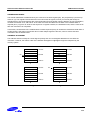
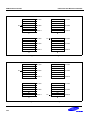
An Example of Scanline Transfer . . . . . . . . . . . . . . . . . . . . . . . . . . . . . . . . . . . . . . . . . .11-8
GEU Special Registers . . . . . . . . . . . . . . . . . . . . . . . . . . . . . . . . . . . . . . . . . . . . . . . . . .11-9
Pattern Page Width Register . . . . . . . . . . . . . . . . . . . . . . . . . . . . . . . . . . . . . . . . . . . . . .11-9
Pattern Start Register . . . . . . . . . . . . . . . . . . . . . . . . . . . . . . . . . . . . . . . . . . . . . . . . . . .11-10
Pattern Width Register . . . . . . . . . . . . . . . . . . . . . . . . . . . . . . . . . . . . . . . . . . . . . . . . . .11-11
Pattern Height Register . . . . . . . . . . . . . . . . . . . . . . . . . . . . . . . . . . . . . . . . . . . . . . . . . .11-12
Immediate Pattern Start Register . . . . . . . . . . . . . . . . . . . . . . . . . . . . . . . . . . . . . . . . . .11-13
Pattern X Remainder Register . . . . . . . . . . . . . . . . . . . . . . . . . . . . . . . . . . . . . . . . . . . . .11-14
Pattern Y Remainder Register . . . . . . . . . . . . . . . . . . . . . . . . . . . . . . . . . . . . . . . . . . . . .11-15
Source Start Register . . . . . . . . . . . . . . . . . . . . . . . . . . . . . . . . . . . . . . . . . . . . . . . . . . .11-16
Source Page Width Register . . . . . . . . . . . . . . . . . . . . . . . . . . . . . . . . . . . . . . . . . . . . . .11-17
Destination Start Register . . . . . . . . . . . . . . . . . . . . . . . . . . . . . . . . . . . . . . . . . . . . . . . .11-18
Destination Page Width Register . . . . . . . . . . . . . . . . . . . . . . . . . . . . . . . . . . . . . . . . . . .11-19
Destination Width Register . . . . . . . . . . . . . . . . . . . . . . . . . . . . . . . . . . . . . . . . . . . . . . .11-20
Destination Height Register . . . . . . . . . . . . . . . . . . . . . . . . . . . . . . . . . . . . . . . . . . . . . . .11-21
GEU Control Register . . . . . . . . . . . . . . . . . . . . . . . . . . . . . . . . . . . . . . . . . . . . . . . . . . .11-22
Band Register . . . . . . . . . . . . . . . . . . . . . . . . . . . . . . . . . . . . . . . . . . . . . . . . . . . . . . . . .11-25
Scanline Table Start Address Register . . . . . . . . . . . . . . . . . . . . . . . . . . . . . . . . . . . . . .11-26
Pattern Companion Table Start Address Register . . . . . . . . . . . . . . . . . . . . . . . . . . . . .11-27
Image Definition Guidelines . . . . . . . . . . . . . . . . . . . . . . . . . . . . . . . . . . . . . . . . . . . . . . .11-28
xii
Table of Contents
12
Imaging Function Block
Image Rotator . . . . . . . . . . . . . . . . . . . . . . . . . . . . . . . . . . . . . . . . . . . . . . . . . . . . . . . . . 12-2
Image Expander . . . . . . . . . . . . . . . . . . . . . . . . . . . . . . . . . . . . . . . . . . . . . . . . . . . . . . . 12-4
Variable Image Scaling (VIS) . . . . . . . . . . . . . . . . . . . . . . . . . . . . . . . . . . . . . . . . . . . . . 12-5
VIS Algorithm . . . . . . . . . . . . . . . . . . . . . . . . . . . . . . . . . . . . . . . . . . . . . . . . . . . . . . . . . 12-6
Example of VIS Operation . . . . . . . . . . . . . . . . . . . . . . . . . . . . . . . . . . . . . . . . . . . . . . . . 12-7
Halftone bit packer . . . . . . . . . . . . . . . . . . . . . . . . . . . . . . . . . . . . . . . . . . . . . . . . . . . . . 12-8
Imaging Special Registers . . . . . . . . . . . . . . . . . . . . . . . . . . . . . . . . . . . . . . . . . . . . . . . . 12-9
Expander/rotator Control Register . . . . . . . . . . . . . . . . . . . . . . . . . . . . . . . . . . . . . . . . . . 12-9
Image Expander Data Registers . . . . . . . . . . . . . . . . . . . . . . . . . . . . . . . . . . . . . . . . . . . 12-10
Image Rotator Data Registers . . . . . . . . . . . . . . . . . . . . . . . . . . . . . . . . . . . . . . . . . . . . . 12-11
VIS/Halftone bit packer Status Register . . . . . . . . . . . . . . . . . . . . . . . . . . . . . . . . . . . . . 12-12
VIS/Halftone bit packer Control Register . . . . . . . . . . . . . . . . . . . . . . . . . . . . . . . . . . . . . 12-13
VIS Data Size Registers . . . . . . . . . . . . . . . . . . . . . . . . . . . . . . . . . . . . . . . . . . . . . . . . . 12-14
VIS Data Registers . . . . . . . . . . . . . . . . . . . . . . . . . . . . . . . . . . . . . . . . . . . . . . . . . . . . . 12-15
Halftone bit packer Data Registers . . . . . . . . . . . . . . . . . . . . . . . . . . . . . . . . . . . . . . . . . 12-16
13
I/O Ports
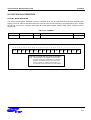
I/O Port Special Registers . . . . . . . . . . . . . . . . . . . . . . . . . . . . . . . . . . . . . . . . . . . . . . . . 13-3
I/O Port Mode Register . . . . . . . . . . . . . . . . . . . . . . . . . . . . . . . . . . . . . . . . . . . . . . . . . . 13-3
External Interrupt Mode Register . . . . . . . . . . . . . . . . . . . . . . . . . . . . . . . . . . . . . . . . . . 13-4
I/O Port Data Register . . . . . . . . . . . . . . . . . . . . . . . . . . . . . . . . . . . . . . . . . . . . . . . . . . . 13-6
I/O Port Timing Diagrams . . . . . . . . . . . . . . . . . . . . . . . . . . . . . . . . . . . . . . . . . . . . . . . . 13-7
14
Interrupt Controller
Interrupt Sources . . . . . . . . . . . . . . . . . . . . . . . . . . . . . . . . . . . . . . . . . . . . . . . . . . . . . . . 14-2
Interrupt Controller Special Registers . . . . . . . . . . . . . . . . . . . . . . . . . . . . . . . . . . . . . . . 14-4
Interrupt Mode Register . . . . . . . . . . . . . . . . . . . . . . . . . . . . . . . . . . . . . . . . . . . . . . . . . . 14-4
Interrupt Pending Register . . . . . . . . . . . . . . . . . . . . . . . . . . . . . . . . . . . . . . . . . . . . . . . 14-5
Interrupt Mask Register . . . . . . . . . . . . . . . . . . . . . . . . . . . . . . . . . . . . . . . . . . . . . . . . . . 14-6
15
Electrical Data
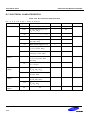
Absolute Maximum Ratings . . . . . . . . . . . . . . . . . . . . . . . . . . . . . . . . . . . . . . . . . . . . . . . 15-1
Thermal Characteristics . . . . . . . . . . . . . . . . . . . . . . . . . . . . . . . . . . . . . . . . . . . . . . . . . 15-1
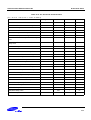
D.C. Electrical charactreristics . . . . . . . . . . . . . . . . . . . . . . . . . . . . . . . . . . . . . . . . . . . . 15-2
Timing Diagram . . . . . . . . . . . . . . . . . . . . . . . . . . . . . . . . . . . . . . . . . . . . . . . . . . . . . . . . 15-5
xiii
Table of Contents
16
Mechanical Data
Package Dimensions . . . . . . . . . . . . . . . . . . . . . . . . . . . . . . . . . . . . . . . . . . . . . . . . . . . .16-1
17
Evaluation Board
Introduction . . . . . . . . . . . . . . . . . . . . . . . . . . . . . . . . . . . . . . . . . . . . . . . . . . . . . . . . . . .17-1
System Requirements . . . . . . . . . . . . . . . . . . . . . . . . . . . . . . . . . . . . . . . . . . . . . . . . . . .17-1
Board Components . . . . . . . . . . . . . . . . . . . . . . . . . . . . . . . . . . . . . . . . . . . . . . . . . . . . .17-1
Changing the Board Configuration . . . . . . . . . . . . . . . . . . . . . . . . . . . . . . . . . . . . . . . . .17-4
Power Input Selection . . . . . . . . . . . . . . . . . . . . . . . . . . . . . . . . . . . . . . . . . . . . . . . . . . .17-4
KS32C6100 Main Clock Frequency Selection . . . . . . . . . . . . . . . . . . . . . . . . . . . . . . . . .17-4
EPROM/Flash Memory Selection . . . . . . . . . . . . . . . . . . . . . . . . . . . . . . . . . . . . . . . . . .17-5
DRAM Banks Configuration . . . . . . . . . . . . . . . . . . . . . . . . . . . . . . . . . . . . . . . . . . . . . . .17-5
Other Configurations . . . . . . . . . . . . . . . . . . . . . . . . . . . . . . . . . . . . . . . . . . . . . . . . . . . .17-5
KS32C6100 Evaluation Board Installation . . . . . . . . . . . . . . . . . . . . . . . . . . . . . . . . . . .17-6
Connecting to Host PC . . . . . . . . . . . . . . . . . . . . . . . . . . . . . . . . . . . . . . . . . . . . . . . . . .17-6
Powering Up . . . . . . . . . . . . . . . . . . . . . . . . . . . . . . . . . . . . . . . . . . . . . . . . . . . . . . . . . .17-6
Booting System . . . . . . . . . . . . . . . . . . . . . . . . . . . . . . . . . . . . . . . . . . . . . . . . . . . . . . . .17-7
EmbeddedICE Unit Installation . . . . . . . . . . . . . . . . . . . . . . . . . . . . . . . . . . . . . . . . . . . .17-8
EmbeddedICE Unit . . . . . . . . . . . . . . . . . . . . . . . . . . . . . . . . . . . . . . . . . . . . . . . . . . . . .17-8
Connecting KS32C6100 Evaluation Board and PC . . . . . . . . . . . . . . . . . . . . . . . . . . . . .17-8
Powering Up the Board and EmbeddedICE . . . . . . . . . . . . . . . . . . . . . . . . . . . . . . . . . .17-8
System Memory Map . . . . . . . . . . . . . . . . . . . . . . . . . . . . . . . . . . . . . . . . . . . . . . . . . . . .17-9
Getting Started with the Example Code . . . . . . . . . . . . . . . . . . . . . . . . . . . . . . . . . . . . .17-10
Download and Run Application on Board without EmbeddedICE . . . . . . . . . . . . . . . . . .17-10
Debug Application with EmbeddedICE . . . . . . . . . . . . . . . . . . . . . . . . . . . . . . . . . . . . . .17-11
Switch and Jumpers Description . . . . . . . . . . . . . . . . . . . . . . . . . . . . . . . . . . . . . . . . . . .17-12
KS32C6100 Evaluation Board Schematic . . . . . . . . . . . . . . . . . . . . . . . . . . . . . . . . . . . .17-14
xiv
List of Figures
1
Product Overview
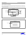
KS32C6100 Block Diagram . . . . . . . . . . . . . . . . . . . . . . . . . . . . . . . . . . . . . . . . . . . . . . . . . . . 1-4
KS32C6100 Pin Assignments . . . . . . . . . . . . . . . . . . . . . . . . . . . . . . . . . . . . . . . . . . . . . . . . . 1-5
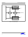
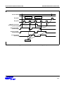
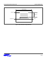
ARM7TDMI Core Block Diagram . . . . . . . . . . . . . . . . . . . . . . . . . . . . . . . . . . . . . . . . . . . . . . . 1-12
2
Programming Model
Register Organization in ARM State . . . . . . . . . . . . . . . . . . . . . . . . . . . . . . . . . . . . . . . . . . . . 2-5
Register Organization in THUMB State . . . . . . . . . . . . . . . . . . . . . . . . . . . . . . . . . . . . . . . . . . 2-6
Mapping of THUMB State Registers onto ARM State Registers . . . . . . . . . . . . . . . . . . . . . . . 2-7
Program Status Register Format (CPSR and SPSR) . . . . . . . . . . . . . . . . . . . . . . . . . . . . . . .2-8
3
Instruction Set
Branch and Exchange Instruction (BX) . . . . . . . . . . . . . . . . . . . . . . . . . . . . . . . . . . . . . . . . . . 3-4
Branch Instructions (B, BL) . . . . . . . . . . . . . . . . . . . . . . . . . . . . . . . . . . . . . . . . . . . . . . . . . . . 3-6
Data Processing Instructions . . . . . . . . . . . . . . . . . . . . . . . . . . . . . . . . . . . . . . . . . . . . . . . . . . 3-9
ARM Shift Operations . . . . . . . . . . . . . . . . . . . . . . . . . . . . . . . . . . . . . . . . . . . . . . . . . . . . . . . 3-11
Logical Shift Left . . . . . . . . . . . . . . . . . . . . . . . . . . . . . . . . . . . . . . . . . . . . . . . . . . . . . . . . . . . 3-12
Logical Shift Right . . . . . . . . . . . . . . . . . . . . . . . . . . . . . . . . . . . . . . . . . . . . . . . . . . . . . . . . . . 3-13
Arithmetic Shift Right . . . . . . . . . . . . . . . . . . . . . . . . . . . . . . . . . . . . . . . . . . . . . . . . . . . . . . . . 3-13
Rotate Right . . . . . . . . . . . . . . . . . . . . . . . . . . . . . . . . . . . . . . . . . . . . . . . . . . . . . . . . . . . . . . . 3-14
Rotate Right Extended . . . . . . . . . . . . . . . . . . . . . . . . . . . . . . . . . . . . . . . . . . . . . . . . . . . . . . . 3-14
MRS (Transfer PSR Contents to a Register) . . . . . . . . . . . . . . . . . . . . . . . . . . . . . . . . . . . . . . 3-19
MRS (Transfer Register Contents to PSR) . . . . . . . . . . . . . . . . . . . . . . . . . . . . . . . . . . . . . . . 3-20
MRS (Transfer Register Contents or Immediate Value to PSR Flag Bits Only) . . . . . . . . . . . 3-20
Multiply and Multiply-Accumulate Instructions . . . . . . . . . . . . . . . . . . . . . . . . . . . . . . . . . . . . . 3-23
Multiply Long and Multiply-Accumulate . . . . . . . . . . . . . . . . . . . . . . . . . . . . . . . . . . . . . . . . . . 3-26
Single Data Transfer Instructions . . . . . . . . . . . . . . . . . . . . . . . . . . . . . . . . . . . . . . . . . . . . . . . 3-29
Little-Endian Offset Addressing . . . . . . . . . . . . . . . . . . . . . . . . . . . . . . . . . . . . . . . . . . . . . . . . 3-31
Half-Word and Signed Data Transfer with Register Offset . . . . . . . . . . . . . . . . . . . . . . . . . . . 3-35
Half-word and Signed Data Transfer with Immediate Offset and Auto-Indexing . . . . . . . . . . . 3-36
Block Data Transfer Instructions . . . . . . . . . . . . . . . . . . . . . . . . . . . . . . . . . . . . . . . . . . . . . . . 3-42
Post-Increment Addressing . . . . . . . . . . . . . . . . . . . . . . . . . . . . . . . . . . . . . . . . . . . . . . . . . . . 3-43
Pre-Increment Addressing . . . . . . . . . . . . . . . . . . . . . . . . . . . . . . . . . . . . . . . . . . . . . . . . . . . . 3-44
Post-Decrement Addressing . . . . . . . . . . . . . . . . . . . . . . . . . . . . . . . . . . . . . . . . . . . . . . . . . . 3-44
Pre-Decrement Addressing . . . . . . . . . . . . . . . . . . . . . . . . . . . . . . . . . . . . . . . . . . . . . . . . . . . 3-45
Swap Instruction . . . . . . . . . . . . . . . . . . . . . . . . . . . . . . . . . . . . . . . . . . . . . . . . . . . . . . . . . . . 3-49
Software Interrupt Instruction . . . . . . . . . . . . . . . . . . . . . . . . . . . . . . . . . . . . . . . . . . . . . . . . . . 3-51
Coprocessor Data Operation Instruction . . . . . . . . . . . . . . . . . . . . . . . . . . . . . . . . . . . . . . . . . 3-53
Coprocessor Data Transfer Instructions . . . . . . . . . . . . . . . . . . . . . . . . . . . . . . . . . . . . . . . . . 3-55
Coprocessor Register Transfer Instructions . . . . . . . . . . . . . . . . . . . . . . . . . . . . . . . . . . . . . . 3-58
xv
List of Figures
Undefined Instruction . . . . . . . . . . . . . . . . . . . . . . . . . . . . . . . . . . . . . . . . . . . . . . . . . . . . . . . .3-61
THUMB Format 1 . . . . . . . . . . . . . . . . . . . . . . . . . . . . . . . . . . . . . . . . . . . . . . . . . . . . . . . . . . .3-71
THUMB Format 2 . . . . . . . . . . . . . . . . . . . . . . . . . . . . . . . . . . . . . . . . . . . . . . . . . . . . . . . . . . .3-73
THUMB Format 3 . . . . . . . . . . . . . . . . . . . . . . . . . . . . . . . . . . . . . . . . . . . . . . . . . . . . . . . . . . .3-75
THUMB Format 4 . . . . . . . . . . . . . . . . . . . . . . . . . . . . . . . . . . . . . . . . . . . . . . . . . . . . . . . . . . .3-77
THUMB Format 5 . . . . . . . . . . . . . . . . . . . . . . . . . . . . . . . . . . . . . . . . . . . . . . . . . . . . . . . . . . .3-79
THUMB Format 6 . . . . . . . . . . . . . . . . . . . . . . . . . . . . . . . . . . . . . . . . . . . . . . . . . . . . . . . . . . .3-82
THUMB Format 7 . . . . . . . . . . . . . . . . . . . . . . . . . . . . . . . . . . . . . . . . . . . . . . . . . . . . . . . . . . .3-83
THUMB Format 8 . . . . . . . . . . . . . . . . . . . . . . . . . . . . . . . . . . . . . . . . . . . . . . . . . . . . . . . . . . .3-85
THUMB Format 9 . . . . . . . . . . . . . . . . . . . . . . . . . . . . . . . . . . . . . . . . . . . . . . . . . . . . . . . . . . .3-87
THUMB Format 10 . . . . . . . . . . . . . . . . . . . . . . . . . . . . . . . . . . . . . . . . . . . . . . . . . . . . . . . . . .3-89
THUMB Format 11 . . . . . . . . . . . . . . . . . . . . . . . . . . . . . . . . . . . . . . . . . . . . . . . . . . . . . . . . . .3-91
THUMB Format 12 . . . . . . . . . . . . . . . . . . . . . . . . . . . . . . . . . . . . . . . . . . . . . . . . . . . . . . . . . .3-93
THUMB Format 13 . . . . . . . . . . . . . . . . . . . . . . . . . . . . . . . . . . . . . . . . . . . . . . . . . . . . . . . . . .3-95
THUMB Format 14 . . . . . . . . . . . . . . . . . . . . . . . . . . . . . . . . . . . . . . . . . . . . . . . . . . . . . . . . . .3-97
THUMB Format 15 . . . . . . . . . . . . . . . . . . . . . . . . . . . . . . . . . . . . . . . . . . . . . . . . . . . . . . . . . .3-99
THUMB Format 16 . . . . . . . . . . . . . . . . . . . . . . . . . . . . . . . . . . . . . . . . . . . . . . . . . . . . . . . . . .3-101
THUMB Format 17 . . . . . . . . . . . . . . . . . . . . . . . . . . . . . . . . . . . . . . . . . . . . . . . . . . . . . . . . . .3-103
THUMB Format 18 . . . . . . . . . . . . . . . . . . . . . . . . . . . . . . . . . . . . . . . . . . . . . . . . . . . . . . . . . .3-105
THUMB Format 19 . . . . . . . . . . . . . . . . . . . . . . . . . . . . . . . . . . . . . . . . . . . . . . . . . . . . . . . . . .3-106
4
System Manager
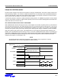
KS32C6100 Address Space . . . . . . . . . . . . . . . . . . . . . . . . . . . . . . . . . . . . . . . . . . . . . . . . . .4-2
System Configuration Register (SYSCFG) . . . . . . . . . . . . . . . . . . . . . . . . . . . . . . . . . . . . . . .4-3
ROM Timing Control Register (ROMTIME) . . . . . . . . . . . . . . . . . . . . . . . . . . . . . . . . . . . . . . .4-4
SRAM Timing Control Register (SRAMTIME) . . . . . . . . . . . . . . . . . . . . . . . . . . . . . . . . . . . . .4-5
DRAM Timing Control Registers . . . . . . . . . . . . . . . . . . . . . . . . . . . . . . . . . . . . . . . . . . . . . . .4-6
External I/O Timing Control Registers . . . . . . . . . . . . . . . . . . . . . . . . . . . . . . . . . . . . . . . . . . .4-7
Data Bus Width Control Register (DBUSWTH) . . . . . . . . . . . . . . . . . . . . . . . . . . . . . . . . . . . .4-8
Memory Bank Address Pointer Registers . . . . . . . . . . . . . . . . . . . . . . . . . . . . . . . . . . . . . . . .4-9
DRAM Refresh Control Register (REFEXTCON) . . . . . . . . . . . . . . . . . . . . . . . . . . . . . . . . . . .4-10
Special I/O Address Map . . . . . . . . . . . . . . . . . . . . . . . . . . . . . . . . . . . . . . . . . . . . . . . . . . . . .4-11
DRAM Refresh Timing . . . . . . . . . . . . . . . . . . . . . . . . . . . . . . . . . . . . . . . . . . . . . . . . . . . . . . .4-12
Self-Refresh Mode Initiated by Hardware (Power-On/nRESET) . . . . . . . . . . . . . . . . . . . . . . .4-13
Self-Refresh Mode Initiated by Hardware (Power-Off/nRESET) . . . . . . . . . . . . . . . . . . . . . . .4-14
Self-Refresh Mode Initiated by Software . . . . . . . . . . . . . . . . . . . . . . . . . . . . . . . . . . . . . . . . .4-15
Initial System Memory Map at System Start-up . . . . . . . . . . . . . . . . . . . . . . . . . . . . . . . . . . . .4-17
Program Example for System Space Reconfiguration . . . . . . . . . . . . . . . . . . . . . . . . . . . . . . .4-19
Example of Mapping External Memory Banks . . . . . . . . . . . . . . . . . . . . . . . . . . . . . . . . . . . . .4-20
Normal Big-Endian System Configuration . . . . . . . . . . . . . . . . . . . . . . . . . . . . . . . . . . . . . . . .4-21
KS32C6100 System Configuration . . . . . . . . . . . . . . . . . . . . . . . . . . . . . . . . . . . . . . . . . . . . .4-22
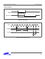
Handshaking Signals Between KS32C6100 and an External Master . . . . . . . . . . . . . . . . . . .4-26
xvi
List of Figures
External Master Access DRAM Timing in Non-Burst Mode . . . . . . . . . . . . . . . . . . . . . . . . . . . 4-28
External Master Access DRAM Timing in Burst Mode . . . . . . . . . . . . . . . . . . . . . . . . . . . . . . . 4-30
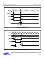
Simple ROM Read Timing (tACC = 6 Cycles) . . . . . . . . . . . . . . . . . . . . . . . . . . . . . . . . . . . . . . 4-31
Simple ROM Write Timing (tACC = 6 Cycles) . . . . . . . . . . . . . . . . . . . . . . . . . . . . . . . . . . . . . . 4-31
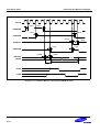
Page Mode ROM Read Timing (tACC = 3, tACP = 2 Cycles) . . . . . . . . . . . . . . . . . . . . . . . . . . 4-32
Page Mode ROM Write Timing (tACC = 3, tACP = 2 Cycles) . . . . . . . . . . . . . . . . . . . . . . . . . . . 4-32
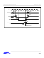
SRAM Read Timing (tACC = 6 Cycles) . . . . . . . . . . . . . . . . . . . . . . . . . . . . . . . . . . . . . . . . . . . 4-33
SRAM Write Timing (tACC = 6 Cycles) . . . . . . . . . . . . . . . . . . . . . . . . . . . . . . . . . . . . . . . . . . . 4-33
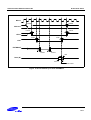
DRAM Read Timing (Page Mode) (tRP = 1, tRC = 2, tCS = 2, tCP = 1, tPGM = 2 Cycles) . . . . .4-34
DRAM Write Timing (Page Mode) (tRP = 1, tRC = 2, tCS = 2, tCP = 1, tPGM = 2 Cycles) . . . . .4-34
External I/O Read Timing (tACS = 2, tCOS = 1, tACC = 4, tCOH = 1 Cycle) . . . . . . . . . . . . . . . . 4-35
External I/O Write Timing (tACS = 2, tCOS = 1, tACC = 4, tCOH = 1 Cycle) . . . . . . . . . . . . . . . . 4-35
Special I/O Read Timing (tACS = 2, tACC = 4, tCOH = 1 Cycle) . . . . . . . . . . . . . . . . . . . . . . 4-36
Special I/O Write Timing (tACS = 2, tACC = 4, tCOH = 1 Cycle) . . . . . . . . . . . . . . . . . . . . . . 4-36
5
Instruction/Data Cache
Non-Cacheable Memory Area Pointer Registers . . . . . . . . . . . . . . . . . . . . . . . . . . . . . . . . . . . 5-3
6
DMA Controller
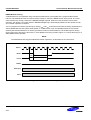
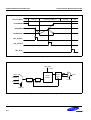
DMA Controller Block Diagram . . . . . . . . . . . . . . . . . . . . . . . . . . . . . . . . . . . . . . . . . . . . . . . . 6-2
Interrupt Generation for DMA Operation (Stop Interrupt Enable Bit is Cleared) . . . . . . . . . . . 6-4
Interrupt Generation for DMA Operation (Stop Interrupt Enable Bit is Set) . . . . . . . . . . . . . . . 6-4
Single Mode Timing Diagram . . . . . . . . . . . . . . . . . . . . . . . . . . . . . . . . . . . . . . . . . . . . . . . . . . 6-5
Block Mode Timing Diagram . . . . . . . . . . . . . . . . . . . . . . . . . . . . . . . . . . . . . . . . . . . . . . . . . . 6-6
Demand Mode Timing Diagram . . . . . . . . . . . . . . . . . . . . . . . . . . . . . . . . . . . . . . . . . . . . . . . . 6-6
Data Compression in Codec Mode . . . . . . . . . . . . . . . . . . . . . . . . . . . . . . . . . . . . . . . . . . . . . 6-7
CDMA Control Register (CDMACON) . . . . . . . . . . . . . . . . . . . . . . . . . . . . . . . . . . . . . . . . . . . 6-11
CDMA Source/Destination Address Registers (CDMASRC, CDMADST) . . . . . . . . . . . . . . . . 6-12
CDMA Transfer Count Register (CDMACNT) . . . . . . . . . . . . . . . . . . . . . . . . . . . . . . . . . . . . . 6-13
GDMA Control Registers (GDMACON0, GDMACON1) . . . . . . . . . . . . . . . . . . . . . . . . . . . . . 6-16
GDMA Source/Destination Address Registers (GDMASRC0/1, GDMADST0/1) . . . . . . . . . . . 6-17
GDMA Transfer Count Registers (GDMACNT0, GDMACNT1) . . . . . . . . . . . . . . . . . . . . . . . . 6-18
7
UART/Serial I/O
Serial I/O Block Diagram . . . . . . . . . . . . . . . . . . . . . . . . . . . . . . . . . . . . . . . . . . . . . . . . . . . . . 7-2
IR Operation Block Diagram . . . . . . . . . . . . . . . . . . . . . . . . . . . . . . . . . . . . . . . . . . . . . . . . . . 7-3
UART/SIO Data Transmit Operation . . . . . . . . . . . . . . . . . . . . . . . . . . . . . . . . . . . . . . . . . . . . 7-6
UART/SIO Data Receive Operation . . . . . . . . . . . . . . . . . . . . . . . . . . . . . . . . . . . . . . . . . . . . . 7-7
UART/SIO Line Control Registers (ULCON0, ULCON1) . . . . . . . . . . . . . . . . . . . . . . . . . . . . . 7-9
UART/SIO Control Registers (UCON0, UCON1) . . . . . . . . . . . . . . . . . . . . . . . . . . . . . . . . . . . 7-11
xvii
List of Figures
UART/SIO Status Registers (USTAT0, USTAT1) . . . . . . . . . . . . . . . . . . . . . . . . . . . . . . . . . .7-13
UART/SIO Transmit Holding Registers (UTXBUF0, UTXBUF1) . . . . . . . . . . . . . . . . . . . . . . .7-14
UART/SIO Receive Buffer Registers (URXBUF0, URXBUF1) . . . . . . . . . . . . . . . . . . . . . . . . .7-15
UART/SIO Baud Rate Divisor Registers (UBRDIV0, UBRDIV1) . . . . . . . . . . . . . . . . . . . . . . .7-16
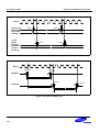
Interrupt-Based Serial I/O Timing Diagram (TX and RX) . . . . . . . . . . . . . . . . . . . . . . . . . . . . .7-17
DMA-Based Serial I/O Timing Diagram (TX only) . . . . . . . . . . . . . . . . . . . . . . . . . . . . . . . . . .7-18
DMA-Based Serial I/O Timing Diagram (RX only) . . . . . . . . . . . . . . . . . . . . . . . . . . . . . . . . . .7-18
Serial I/O Frame Timing Diagram (Normal UART) . . . . . . . . . . . . . . . . . . . . . . . . . . . . . . . . . .7-19
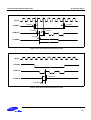
Infra-Red Transmit Mode Frame Timing Diagram . . . . . . . . . . . . . . . . . . . . . . . . . . . . . . . . . .7-19
Infra-Red Receive Mode Frame Timing Diagram . . . . . . . . . . . . . . . . . . . . . . . . . . . . . . . . . . .7-19
8
Parallel Port
Compatibility Hardware Handshaking Timing . . . . . . . . . . . . . . . . . . . . . . . . . . . . . . . . . . . . .8-3
ECP Hardware Handshaking Timing (Forward) . . . . . . . . . . . . . . . . . . . . . . . . . . . . . . . . . . . .8-5
ECP Hardware Handshaking Timing (Reverse) . . . . . . . . . . . . . . . . . . . . . . . . . . . . . . . . . . . .8-5
Parallel Port Data Register (PPDATA) . . . . . . . . . . . . . . . . . . . . . . . . . . . . . . . . . . . . . . . . . . .8-6
Parallel Port Status Register (PPSTAT) . . . . . . . . . . . . . . . . . . . . . . . . . . . . . . . . . . . . . . . . . .8-8
Parallel Port ACK Width Register (PPACKWTH) . . . . . . . . . . . . . . . . . . . . . . . . . . . . . . . . . . .8-10
Parallel Port Control Register (PPCON) . . . . . . . . . . . . . . . . . . . . . . . . . . . . . . . . . . . . . . . . . .8-12
Parallel Port Interrupt Enable Register (PPINTEN) . . . . . . . . . . . . . . . . . . . . . . . . . . . . . . . . .8-17
Parallel Port Interrupt Pending Register (PPINTPND) . . . . . . . . . . . . . . . . . . . . . . . . . . . . . . .8-18
9
Programmable Timers
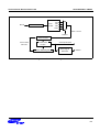
Block Diagram of Timers 0, 2-4 . . . . . . . . . . . . . . . . . . . . . . . . . . . . . . . . . . . . . . . . . . . . . . . .9-2
Timer 1 Block Diagram . . . . . . . . . . . . . . . . . . . . . . . . . . . . . . . . . . . . . . . . . . . . . . . . . . . . . . .9-3
Mode Registers for TMOD0 and TMOD2–4 . . . . . . . . . . . . . . . . . . . . . . . . . . . . . . . . . . . . . . .9-4
Timer 1 Mode Register (TMOD1) . . . . . . . . . . . . . . . . . . . . . . . . . . . . . . . . . . . . . . . . . . . . . . .9-5
Timer Data Registers (TDATA0–TDATA4) . . . . . . . . . . . . . . . . . . . . . . . . . . . . . . . . . . . . . . .9-8
Timer Count Registers (TCNT0–TCNT4) . . . . . . . . . . . . . . . . . . . . . . . . . . . . . . . . . . . . . . . . .9-9
10
Printer Interface Controller
Message Communication Interface . . . . . . . . . . . . . . . . . . . . . . . . . . . . . . . . . . . . . . . . . . . . .10-2
Command Message Transfers from KS32C6100 to Printer Engine . . . . . . . . . . . . . . . . . . . . .10-3
Printer Engine Message Transfers from Engine to KS32C6100 . . . . . . . . . . . . . . . . . . . . . . .10-3
Queued Operation for End-of-Page (EOP) . . . . . . . . . . . . . . . . . . . . . . . . . . . . . . . . . . . . . . .10-5
Queued Operation for Page Underrun (PUR) . . . . . . . . . . . . . . . . . . . . . . . . . . . . . . . . . . . . .10-6
Print Protocol Transfer Signals Between KS32C6100 and Printer Engine . . . . . . . . . . . . . . .10-7
Protocol Diagram (PIFC and Printer Engine) . . . . . . . . . . . . . . . . . . . . . . . . . . . . . . . . . . . . . .10-8
Video Output Block Diagram . . . . . . . . . . . . . . . . . . . . . . . . . . . . . . . . . . . . . . . . . . . . . . . . . .10-8
PIFC Transmit Buffer Register (PITXBUF) . . . . . . . . . . . . . . . . . . . . . . . . . . . . . . . . . . . . . . . .10-9
xviii
List of Figures
PIFC Receive Buffer Register (PIRXBUF) . . . . . . . . . . . . . . . . . . . . . . . . . . . . . . . . . . . . . . . . 10-10
Command Mode Register (PICMOD) . . . . . . . . . . . . . . . . . . . . . . . . . . . . . . . . . . . . . . . . . . . 10-12
PDMA and Engine Interface Status Register (PISTAT) . . . . . . . . . . . . . . . . . . . . . . . . . . . . . . 10-14
Video Control Register (PIVCON) . . . . . . . . . . . . . . . . . . . . . . . . . . . . . . . . . . . . . . . . . . . . . . 10-16
Pattern Control Register (PIPCON) . . . . . . . . . . . . . . . . . . . . . . . . . . . . . . . . . . . . . . . . . . . . . 10-17
Printer DMA Control Register (PDMACON) . . . . . . . . . . . . . . . . . . . . . . . . . . . . . . . . . . . . . . . 10-20
Top Margin Register (PITOPMG) . . . . . . . . . . . . . . . . . . . . . . . . . . . . . . . . . . . . . . . . . . . . . . 10-21
Page Layout . . . . . . . . . . . . . . . . . . . . . . . . . . . . . . . . . . . . . . . . . . . . . . . . . . . . . . . . . . . . . . . 10-21
Left Margin Register (PILFTMG) . . . . . . . . . . . . . . . . . . . . . . . . . . . . . . . . . . . . . . . . . . . . . . . 10-22
Pixel Count Register (PIPXLCNT) . . . . . . . . . . . . . . . . . . . . . . . . . . . . . . . . . . . . . . . . . . . . . . 10-23
Queue 0/1 Start Address Registers (PDMASRC0, PDMASRC1) . . . . . . . . . . . . . . . . . . . . . . 10-24
Queue 0/1 Transfer Count Registers (PDMACNT0, PDMACNT1) . . . . . . . . . . . . . . . . . . . . . 10-25
11
Graphic Engine Unit
Boolean Operations for Graphic Processing . . . . . . . . . . . . . . . . . . . . . . . . . . . . . . . . . . . . . . 11-2
Sample Graphic Operation . . . . . . . . . . . . . . . . . . . . . . . . . . . . . . . . . . . . . . . . . . . . . . . . . . . 11-2
Bit String Specifier Formats . . . . . . . . . . . . . . . . . . . . . . . . . . . . . . . . . . . . . . . . . . . . . . . . . . . 11-4
32-Bit Pattern Specifier Format . . . . . . . . . . . . . . . . . . . . . . . . . . . . . . . . . . . . . . . . . . . . . . . . 11-7
48-Bit Pattern Specifier Format . . . . . . . . . . . . . . . . . . . . . . . . . . . . . . . . . . . . . . . . . . . . . . . . 11-7
Scanline and Pattern Table Example . . . . . . . . . . . . . . . . . . . . . . . . . . . . . . . . . . . . . . . . . . . . 11-8
Pattern Page Width Register (GPATPGWTH) . . . . . . . . . . . . . . . . . . . . . . . . . . . . . . . . . . . . . 11-9
Pattern Start Register (GPATSA) . . . . . . . . . . . . . . . . . . . . . . . . . . . . . . . . . . . . . . . . . . . . . . 11-10
Pattern Width Register (GPATWTH) . . . . . . . . . . . . . . . . . . . . . . . . . . . . . . . . . . . . . . . . . . . . 11-11
Pattern Height Register (GPATHT) . . . . . . . . . . . . . . . . . . . . . . . . . . . . . . . . . . . . . . . . . . . . . 11-12
Immediate Pattern Start Register (GPATISA) . . . . . . . . . . . . . . . . . . . . . . . . . . . . . . . . . . . . . 11-13
Pattern X Remainder Register (GPATXR) . . . . . . . . . . . . . . . . . . . . . . . . . . . . . . . . . . . . . . . . 11-14
Pattern Y Remainder Register (GPATYR) . . . . . . . . . . . . . . . . . . . . . . . . . . . . . . . . . . . . . . . . 11-15
Source Start Register (GSRCSA) . . . . . . . . . . . . . . . . . . . . . . . . . . . . . . . . . . . . . . . . . . . . . . 11-16
Source Page Width Register (GSRCPGWTH) . . . . . . . . . . . . . . . . . . . . . . . . . . . . . . . . . . . . 11-17
Destination Start Register (GDSTSA) . . . . . . . . . . . . . . . . . . . . . . . . . . . . . . . . . . . . . . . . . . . 11-18
Destination Page Width Register (GDSTPGWTH) . . . . . . . . . . . . . . . . . . . . . . . . . . . . . . . . . 11-19
Destination Width Register (GDSTWTH) . . . . . . . . . . . . . . . . . . . . . . . . . . . . . . . . . . . . . . . . .11-20
Destination Height Register (GDSTHT) . . . . . . . . . . . . . . . . . . . . . . . . . . . . . . . . . . . . . . . . . . 11-21
GEU Control Register (GCON) . . . . . . . . . . . . . . . . . . . . . . . . . . . . . . . . . . . . . . . . . . . . . . . . 11-23
Band Register (GBANDPTR) . . . . . . . . . . . . . . . . . . . . . . . . . . . . . . . . . . . . . . . . . . . . . . . . . . 11-25
Scanline Table Start Address Register (GSLTSA) . . . . . . . . . . . . . . . . . . . . . . . . . . . . . . . . . 11-26
Pattern Companion Table Start Address Register (GPCTSA) . . . . . . . . . . . . . . . . . . . . . . . . . 11-27
Pattern Image Definition . . . . . . . . . . . . . . . . . . . . . . . . . . . . . . . . . . . . . . . . . . . . . . . . . . . . . 11-28
Source Image Definition . . . . . . . . . . . . . . . . . . . . . . . . . . . . . . . . . . . . . . . . . . . . . . . . . . . . . .11-28
Destination Image Definition . . . . . . . . . . . . . . . . . . . . . . . . . . . . . . . . . . . . . . . . . . . . . . . . . . 11-29
xix
List of Figures
12
Imaging Function Block
Image Rotation Operation . . . . . . . . . . . . . . . . . . . . . . . . . . . . . . . . . . . . . . . . . . . . . . . . . . . .12-2
An Example of Image Rotation . . . . . . . . . . . . . . . . . . . . . . . . . . . . . . . . . . . . . . . . . . . . . . . .12-3
Image Expansion Operation . . . . . . . . . . . . . . . . . . . . . . . . . . . . . . . . . . . . . . . . . . . . . . . . . . .12-4
VIS Algorithm . . . . . . . . . . . . . . . . . . . . . . . . . . . . . . . . . . . . . . . . . . . . . . . . . . . . . . . . . . . . . .12-6
Example of VIS Internal Operation . . . . . . . . . . . . . . . . . . . . . . . . . . . . . . . . . . . . . . . . . . . . . .12-7
Halftoning Algorithm . . . . . . . . . . . . . . . . . . . . . . . . . . . . . . . . . . . . . . . . . . . . . . . . . . . . . . . . .12-8
Expander/Rotator Control Register (EXPROTCON) . . . . . . . . . . . . . . . . . . . . . . . . . . . . . . . .12-9
Expander Data Registers (EXPDATA0–EXPDATA2) . . . . . . . . . . . . . . . . . . . . . . . . . . . . . . .12-10
Image Rotator Data Registers (ROTDATA0–ROTDATA15) . . . . . . . . . . . . . . . . . . . . . . . . . .12-11
VIS/Halftone Bit Packer Status Register (VISHTSTAT) . . . . . . . . . . . . . . . . . . . . . . . . . . . . . .12-12
VIS/Halftone Bit Packer Control Register (VISHTCON) . . . . . . . . . . . . . . . . . . . . . . . . . . . . . .12-13
VIS Data Size Registers (VISDDSIZE, VISSDSIZE) . . . . . . . . . . . . . . . . . . . . . . . . . . . . . . . .12-14
VIS Data Registers (VISSDATA, VISDDATA) . . . . . . . . . . . . . . . . . . . . . . . . . . . . . . . . . . . . .12-15
Halftone Bit Packer Data Registers (HTRDATA, HTSDATA, and HTDATA) . . . . . . . . . . . . . .12-16
13
I/O Ports
I/O Port Mode Register (IOPMOD) . . . . . . . . . . . . . . . . . . . . . . . . . . . . . . . . . . . . . . . . . . . . .13-3
External Interrupt Mode Register (EXTINTMOD) . . . . . . . . . . . . . . . . . . . . . . . . . . . . . . . . . . .13-4
I/O Port Data Register (IOPDATA) . . . . . . . . . . . . . . . . . . . . . . . . . . . . . . . . . . . . . . . . . . . . . .13-6
External Interrupt Timing When ExtIREQ is Active High . . . . . . . . . . . . . . . . . . . . . . . . . . . . .13-7
External Interrupt Timing When ExtIREQ is Active Low . . . . . . . . . . . . . . . . . . . . . . . . . . . . . .13-7
14
Interrupt Controller
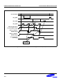
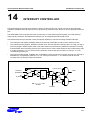
Interrupt Controller Block Diagram . . . . . . . . . . . . . . . . . . . . . . . . . . . . . . . . . . . . . . . . . . . . . .14-1
Interrupt Mode Register (INTMOD) . . . . . . . . . . . . . . . . . . . . . . . . . . . . . . . . . . . . . . . . . . . . .14-4
Interrupt Pending Register (INTPND) . . . . . . . . . . . . . . . . . . . . . . . . . . . . . . . . . . . . . . . . . . .14-5
Interrupt Mask Register (INTMSK) . . . . . . . . . . . . . . . . . . . . . . . . . . . . . . . . . . . . . . . . . . . . . .14-6
15
Electrical Data
Reset Cycles . . . . . . . . . . . . . . . . . . . . . . . . . . . . . . . . . . . . . . . . . . . . . . . . . . . . . . . . . . . . . .15-5
External Interrupt Cycle . . . . . . . . . . . . . . . . . . . . . . . . . . . . . . . . . . . . . . . . . . . . . . . . . . . . . .15-5
Parallel Port Interface Cycle . . . . . . . . . . . . . . . . . . . . . . . . . . . . . . . . . . . . . . . . . . . . . . . . . . .15-6
External DMA Cycle . . . . . . . . . . . . . . . . . . . . . . . . . . . . . . . . . . . . . . . . . . . . . . . . . . . . . . . . .15-6
Print Engine Interface Cycle #1 . . . . . . . . . . . . . . . . . . . . . . . . . . . . . . . . . . . . . . . . . . . . . . . .15-7
Print Engine Interface Cycle #2 . . . . . . . . . . . . . . . . . . . . . . . . . . . . . . . . . . . . . . . . . . . . . . . .15-7
Print Engine Interface Cycle #3 . . . . . . . . . . . . . . . . . . . . . . . . . . . . . . . . . . . . . . . . . . . . . . . .15-8
Print Engine Interface Cycle #4 . . . . . . . . . . . . . . . . . . . . . . . . . . . . . . . . . . . . . . . . . . . . . . . .15-8
ROM Read Timing . . . . . . . . . . . . . . . . . . . . . . . . . . . . . . . . . . . . . . . . . . . . . . . . . . . . . . . . . .15-9
xx
List of Figures
ROM Write Timing . . . . . . . . . . . . . . . . . . . . . . . . . . . . . . . . . . . . . . . . . . . . . . . . . . . . . . . . . . 15-9
ROM Page Read . . . . . . . . . . . . . . . . . . . . . . . . . . . . . . . . . . . . . . . . . . . . . . . . . . . . . . . . . . . 15-10
ROM Page Write . . . . . . . . . . . . . . . . . . . . . . . . . . . . . . . . . . . . . . . . . . . . . . . . . . . . . . . . . . . 15-10
DRAM Read Cycle . . . . . . . . . . . . . . . . . . . . . . . . . . . . . . . . . . . . . . . . . . . . . . . . . . . . . . . . . . 15-11
DRAM Write Cycle . . . . . . . . . . . . . . . . . . . . . . . . . . . . . . . . . . . . . . . . . . . . . . . . . . . . . . . . . . 15-12
SRAM Read Cycle . . . . . . . . . . . . . . . . . . . . . . . . . . . . . . . . . . . . . . . . . . . . . . . . . . . . . . . . . . 15-13
SRAM Write Cycle . . . . . . . . . . . . . . . . . . . . . . . . . . . . . . . . . . . . . . . . . . . . . . . . . . . . . . . . . . 15-13
External Master Timing (Only DRAM Access) . . . . . . . . . . . . . . . . . . . . . . . . . . . . . . . . . . . . . 15-14
ECS Read Cycle . . . . . . . . . . . . . . . . . . . . . . . . . . . . . . . . . . . . . . . . . . . . . . . . . . . . . . . . . . . 15-15
ECS Write Cycle . . . . . . . . . . . . . . . . . . . . . . . . . . . . . . . . . . . . . . . . . . . . . . . . . . . . . . . . . . . 15-16
ECS Read Cycle with EXTNWAIT . . . . . . . . . . . . . . . . . . . . . . . . . . . . . . . . . . . . . . . . . . . . . . 15-17
ECS Write Cycle with EXTNWAIT . . . . . . . . . . . . . . . . . . . . . . . . . . . . . . . . . . . . . . . . . . . . . . 15-18
Special I/O Read Cycle . . . . . . . . . . . . . . . . . . . . . . . . . . . . . . . . . . . . . . . . . . . . . . . . . . . . . . 15-19
Special I/O Write Cycle . . . . . . . . . . . . . . . . . . . . . . . . . . . . . . . . . . . . . . . . . . . . . . . . . . . . . . 15-20
16
Mechanical Data
208-QFP Package Dimensions. . . . . . . . . . . . . . . . . . . . . . . . . . . . . . . . . . . . . . . . . . . . . . . . . 16-1
17
Evaluation Board
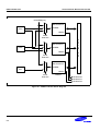
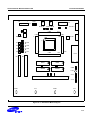
Evaluation Board Layout . . . . . . . . . . . . . . . . . . . . . . . . . . . . . . . . . . . . . . . . . . . . . . . . . . . . . 17-3
Connection to Host PC . . . . . . . . . . . . . . . . . . . . . . . . . . . . . . . . . . . . . . . . . . . . . . . . . . . . . . 17-7
Connection with EmbeddedICE . . . . . . . . . . . . . . . . . . . . . . . . . . . . . . . . . . . . . . . . . . . . . . . . 17-7
Default System Memory Map . . . . . . . . . . . . . . . . . . . . . . . . . . . . . . . . . . . . . . . . . . . . . . . . . . 17-9
Evaluation Board Schematic . . . . . . . . . . . . . . . . . . . . . . . . . . . . . . . . . . . . . . . . . . . . . . . . . . 17-14
xxi
List of Tables
1
Product Overview
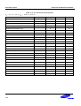
KS32C6100 Signal Descriptions . . . . . . . . . . . . . . . . . . . . . . . . . . . . . . . . . . . . . . . . . . . . . . . . . 1-6
KS32C6100 Pin Type Descriptions . . . . . . . . . . . . . . . . . . . . . . . . . . . . . . . . . . . . . . . . . . . . . . . 1-11
KS32C6100 Special Registers . . . . . . . . . . . . . . . . . . . . . . . . . . . . . . . . . . . . . . . . . . . . . . . . . . . 1-15
2
Programming Model
Big-Endian Addresses of Bytes Within Words . . . . . . . . . . . . . . . . . . . . . . . . . . . . . . . . . . . . . . . 2-2
Little-Endian Addresses of Bytes within Words . . . . . . . . . . . . . . . . . . . . . . . . . . . . . . . . . . . . . . 2-2
ARM State Registers R14–R16 . . . . . . . . . . . . . . . . . . . . . . . . . . . . . . . . . . . . . . . . . . . . . . . . . . 2-4
Program Status Register (PSR) Control Bits . . . . . . . . . . . . . . . . . . . . . . . . . . . . . . . . . . . . . . . . 2-9
PSR Mode Bit Values . . . . . . . . . . . . . . . . . . . . . . . . . . . . . . . . . . . . . . . . . . . . . . . . . . . . . . . . . . 2-10
Exception Entry/Exit Summary . . . . . . . . . . . . . . . . . . . . . . . . . . . . . . . . . . . . . . . . . . . . . . . . . . . 2-12
Exception Vectors . . . . . . . . . . . . . . . . . . . . . . . . . . . . . . . . . . . . . . . . . . . . . . . . . . . . . . . . . . . . 2-14
3
Instruction Set
ARM Instruction Set Formats . . . . . . . . . . . . . . . . . . . . . . . . . . . . . . . . . . . . . . . . . . . . . . . . . . . . 3-1
The ARM Instruction Set . . . . . . . . . . . . . . . . . . . . . . . . . . . . . . . . . . . . . . . . . . . . . . . . . . . . . . . 3-2
Condition Code Summary . . . . . . . . . . . . . . . . . . . . . . . . . . . . . . . . . . . . . . . . . . . . . . . . . . . . . .3-3
ARM Data Processing Instructions . . . . . . . . . . . . . . . . . . . . . . . . . . . . . . . . . . . . . . . . . . . . . . . 3-10
Syntax Descriptions for MULL and MLAL . . . . . . . . . . . . . . . . . . . . . . . . . . . . . . . . . . . . . . . . . . 3-28
Addressing Mode Names . . . . . . . . . . . . . . . . . . . . . . . . . . . . . . . . . . . . . . . . . . . . . . . . . . . . . . . 3-47
THUMB Instruction Set Formats . . . . . . . . . . . . . . . . . . . . . . . . . . . . . . . . . . . . . . . . . . . . . . . . . . 3-68
THUMB Instructions and Opcodes . . . . . . . . . . . . . . . . . . . . . . . . . . . . . . . . . . . . . . . . . . . . . . . . 3-69
Summary of Format 1 Instructions . . . . . . . . . . . . . . . . . . . . . . . . . . . . . . . . . . . . . . . . . . . . . . . . 3-71
Summary of Format 2 Instructions . . . . . . . . . . . . . . . . . . . . . . . . . . . . . . . . . . . . . . . . . . . . . . . . 3-73
Summary of Format 3 Instructions . . . . . . . . . . . . . . . . . . . . . . . . . . . . . . . . . . . . . . . . . . . . . . . . 3-75
Summary of Format 4 Instructions . . . . . . . . . . . . . . . . . . . . . . . . . . . . . . . . . . . . . . . . . . . . . . . . 3-77
Summary of Format 5 Instructions . . . . . . . . . . . . . . . . . . . . . . . . . . . . . . . . . . . . . . . . . . . . . . . . 3-80
Summary of Format 6 Instructions . . . . . . . . . . . . . . . . . . . . . . . . . . . . . . . . . . . . . . . . . . . . . . . . 3-82
Summary of Format 7 Instructions . . . . . . . . . . . . . . . . . . . . . . . . . . . . . . . . . . . . . . . . . . . . . . . . 3-83
Summary of Format 8 Instructions . . . . . . . . . . . . . . . . . . . . . . . . . . . . . . . . . . . . . . . . . . . . . . . . 3-85
Summary of Format 9 Instructions . . . . . . . . . . . . . . . . . . . . . . . . . . . . . . . . . . . . . . . . . . . . . . . . 3-87
Summary of Format 10 Instructions . . . . . . . . . . . . . . . . . . . . . . . . . . . . . . . . . . . . . . . . . . . . . . . 3-89
Summary of Format 11 Instructions . . . . . . . . . . . . . . . . . . . . . . . . . . . . . . . . . . . . . . . . . . . . . . . 3-91
Summary of Format 12 Instructions . . . . . . . . . . . . . . . . . . . . . . . . . . . . . . . . . . . . . . . . . . . . . . . 3-93
Summary of Format 13 Instructions . . . . . . . . . . . . . . . . . . . . . . . . . . . . . . . . . . . . . . . . . . . . . . . 3-95
Summary of Format 14 Instructions . . . . . . . . . . . . . . . . . . . . . . . . . . . . . . . . . . . . . . . . . . . . . . . 3-97
Summary of Format 15 Instructions . . . . . . . . . . . . . . . . . . . . . . . . . . . . . . . . . . . . . . . . . . . . . . . 3-99
Summary of Format 16 Instructions . . . . . . . . . . . . . . . . . . . . . . . . . . . . . . . . . . . . . . . . . . . . . . . 3-101
Summary of Format 17 Instructions . . . . . . . . . . . . . . . . . . . . . . . . . . . . . . . . . . . . . . . . . . . . . . . 3-103
xxiii
List of Tables
Summary of Format 18 Instructions . . . . . . . . . . . . . . . . . . . . . . . . . . . . . . . . . . . . . . . . . . . . . . .3-105
Summary of Format 19 Instructions . . . . . . . . . . . . . . . . . . . . . . . . . . . . . . . . . . . . . . . . . . . . . . .3-106
4
System Manager
SYSCFG . . . . . . . . . . . . . . . . . . . . . . . . . . . . . . . . . . . . . . . . . . . . . . . . . . . . . . . . . . . . . . . . . . . .4-3
ROMTIME . . . . . . . . . . . . . . . . . . . . . . . . . . . . . . . . . . . . . . . . . . . . . . . . . . . . . . . . . . . . . . . . . . .4-4
SRAMTIME . . . . . . . . . . . . . . . . . . . . . . . . . . . . . . . . . . . . . . . . . . . . . . . . . . . . . . . . . . . . . . . . . .4-5
DRAMTIME0–DRAMTIME2 . . . . . . . . . . . . . . . . . . . . . . . . . . . . . . . . . . . . . . . . . . . . . . . . . . . . .4-6
EXTTIME0 and EXTTIME1 . . . . . . . . . . . . . . . . . . . . . . . . . . . . . . . . . . . . . . . . . . . . . . . . . . . . .4-7
DBUSWTH . . . . . . . . . . . . . . . . . . . . . . . . . . . . . . . . . . . . . . . . . . . . . . . . . . . . . . . . . . . . . . . . . .4-8
BANKPTR0–BANKPTR10 . . . . . . . . . . . . . . . . . . . . . . . . . . . . . . . . . . . . . . . . . . . . . . . . . . . . . .4-9
REFEXTCON . . . . . . . . . . . . . . . . . . . . . . . . . . . . . . . . . . . . . . . . . . . . . . . . . . . . . . . . . . . . . . . .4-10
Bus Arbitration Priorities and Maximum Latencies . . . . . . . . . . . . . . . . . . . . . . . . . . . . . . . . . . . .4-23
ExtMAS[1:0] Values . . . . . . . . . . . . . . . . . . . . . . . . . . . . . . . . . . . . . . . . . . . . . . . . . . . . . . . . . . .4-24
ExtMBST Values . . . . . . . . . . . . . . . . . . . . . . . . . . . . . . . . . . . . . . . . . . . . . . . . . . . . . . . . . . . . .4-24
5
Instruction/Data Cache
Cache Special Registers . . . . . . . . . . . . . . . . . . . . . . . . . . . . . . . . . . . . . . . . . . . . . . . . . . . . . . .5-3
6
DMA Controller
Differences between GDMA and CDMA . . . . . . . . . . . . . . . . . . . . . . . . . . . . . . . . . . . . . . . . . . .6-5
CDMACON . . . . . . . . . . . . . . . . . . . . . . . . . . . . . . . . . . . . . . . . . . . . . . . . . . . . . . . . . . . . . . . . . .6-8
CDMACON Register Description . . . . . . . . . . . . . . . . . . . . . . . . . . . . . . . . . . . . . . . . . . . . . . . . .6-8
CDMASRC and CDMADST . . . . . . . . . . . . . . . . . . . . . . . . . . . . . . . . . . . . . . . . . . . . . . . . . . . . .6-12
CDMACNT . . . . . . . . . . . . . . . . . . . . . . . . . . . . . . . . . . . . . . . . . . . . . . . . . . . . . . . . . . . . . . . . . .6-13
GDMACON0 and GDMACON1 . . . . . . . . . . . . . . . . . . . . . . . . . . . . . . . . . . . . . . . . . . . . . . . . . .6-14
GDMACON0/GDMACON1 Register Description . . . . . . . . . . . . . . . . . . . . . . . . . . . . . . . . . . . . .6-14
GDMASRC0/1 and GDMADST0/1 . . . . . . . . . . . . . . . . . . . . . . . . . . . . . . . . . . . . . . . . . . . . . . . .6-17
GDMACNT0 and GDMACNT1 . . . . . . . . . . . . . . . . . . . . . . . . . . . . . . . . . . . . . . . . . . . . . . . . . . .6-18
7
UART/Serial I/O
ULCON0 and ULCON1 . . . . . . . . . . . . . . . . . . . . . . . . . . . . . . . . . . . . . . . . . . . . . . . . . . . . . . . .7-8
ULCON0/ULCON1 Register Description . . . . . . . . . . . . . . . . . . . . . . . . . . . . . . . . . . . . . . . . . . .7-8
UCON0 and UCON1 . . . . . . . . . . . . . . . . . . . . . . . . . . . . . . . . . . . . . . . . . . . . . . . . . . . . . . . . . .7-10
UCON0/UCON1 Register Description . . . . . . . . . . . . . . . . . . . . . . . . . . . . . . . . . . . . . . . . . . . . .7-10
USTAT0 and USTAT1 . . . . . . . . . . . . . . . . . . . . . . . . . . . . . . . . . . . . . . . . . . . . . . . . . . . . . . . . .7-11
USTAT0/USTAT1 Register Description . . . . . . . . . . . . . . . . . . . . . . . . . . . . . . . . . . . . . . . . . . . .7-12
UTXBUF0 and UTXBUF1 . . . . . . . . . . . . . . . . . . . . . . . . . . . . . . . . . . . . . . . . . . . . . . . . . . . . . . .7-14
UTXBUF0/UTXBUF1 Register Description . . . . . . . . . . . . . . . . . . . . . . . . . . . . . . . . . . . . . . . . .7-14
xxiv
List of Tables
URXBUF0 and URXBUF1 . . . . . . . . . . . . . . . . . . . . . . . . . . . . . . . . . . . . . . . . . . . . . . . . . . . . . . 7-15
URXBUF0/URXBUF1 Register Description . . . . . . . . . . . . . . . . . . . . . . . . . . . . . . . . . . . . . . . . .7-15
UBRDIV0 and UBRDIV1 . . . . . . . . . . . . . . . . . . . . . . . . . . . . . . . . . . . . . . . . . . . . . . . . . . . . . . . 7-16
8
Parallel Port
PPDATA . . . . . . . . . . . . . . . . . . . . . . . . . . . . . . . . . . . . . . . . . . . . . . . . . . . . . . . . . . . . . . . . . . . . 8-6
PPSTAT . . . . . . . . . . . . . . . . . . . . . . . . . . . . . . . . . . . . . . . . . . . . . . . . . . . . . . . . . . . . . . . . . . . . 8-7
PPSTAT Register Description . . . . . . . . . . . . . . . . . . . . . . . . . . . . . . . . . . . . . . . . . . . . . . . . . . . 8-9
PPACKWTH . . . . . . . . . . . . . . . . . . . . . . . . . . . . . . . . . . . . . . . . . . . . . . . . . . . . . . . . . . . . . . . . . 8-10
PPCON . . . . . . . . . . . . . . . . . . . . . . . . . . . . . . . . . . . . . . . . . . . . . . . . . . . . . . . . . . . . . . . . . . . . 8-11
PPCON Register Description . . . . . . . . . . . . . . . . . . . . . . . . . . . . . . . . . . . . . . . . . . . . . . . . . . . . 8-13
PPINTEN and PPINTPND . . . . . . . . . . . . . . . . . . . . . . . . . . . . . . . . . . . . . . . . . . . . . . . . . . . . . .8-15
PPINTPND Register Description . . . . . . . . . . . . . . . . . . . . . . . . . . . . . . . . . . . . . . . . . . . . . . . . . 8-16
9
Programmable Timers
TMOD0–TMOD4 . . . . . . . . . . . . . . . . . . . . . . . . . . . . . . . . . . . . . . . . . . . . . . . . . . . . . . . . . . . . .9-4
TMOD0 and TMOD2–4 Register Description . . . . . . . . . . . . . . . . . . . . . . . . . . . . . . . . . . . . . . . . 9-6
TMOD1 Register Description . . . . . . . . . . . . . . . . . . . . . . . . . . . . . . . . . . . . . . . . . . . . . . . . . . . . 9-7
TDATA0–TDATA4 . . . . . . . . . . . . . . . . . . . . . . . . . . . . . . . . . . . . . . . . . . . . . . . . . . . . . . . . . . . . 9-8
TCNT0–TCNT4 . . . . . . . . . . . . . . . . . . . . . . . . . . . . . . . . . . . . . . . . . . . . . . . . . . . . . . . . . . . . . .9-9
10
Printer Interface Controller
PITXBUF . . . . . . . . . . . . . . . . . . . . . . . . . . . . . . . . . . . . . . . . . . . . . . . . . . . . . . . . . . . . . . . . . . . 10-9
PIRXBUF . . . . . . . . . . . . . . . . . . . . . . . . . . . . . . . . . . . . . . . . . . . . . . . . . . . . . . . . . . . . . . . . . . . 10-10
PICMOD . . . . . . . . . . . . . . . . . . . . . . . . . . . . . . . . . . . . . . . . . . . . . . . . . . . . . . . . . . . . . . . . . . . . 10-11
PICMOD Register Description . . . . . . . . . . . . . . . . . . . . . . . . . . . . . . . . . . . . . . . . . . . . . . . . . . . 10-11
PISTAT . . . . . . . . . . . . . . . . . . . . . . . . . . . . . . . . . . . . . . . . . . . . . . . . . . . . . . . . . . . . . . . . . . . . . 10-13
PISTAT Register Description . . . . . . . . . . . . . . . . . . . . . . . . . . . . . . . . . . . . . . . . . . . . . . . . . . . . 10-13
PIVCON . . . . . . . . . . . . . . . . . . . . . . . . . . . . . . . . . . . . . . . . . . . . . . . . . . . . . . . . . . . . . . . . . . . . 10-15
PIVCON Register Description . . . . . . . . . . . . . . . . . . . . . . . . . . . . . . . . . . . . . . . . . . . . . . . . . . . 10-15
PIPCON . . . . . . . . . . . . . . . . . . . . . . . . . . . . . . . . . . . . . . . . . . . . . . . . . . . . . . . . . . . . . . . . . . . . 10-17
PIPCON Register Description . . . . . . . . . . . . . . . . . . . . . . . . . . . . . . . . . . . . . . . . . . . . . . . . . . . 10-18
PDMACON . . . . . . . . . . . . . . . . . . . . . . . . . . . . . . . . . . . . . . . . . . . . . . . . . . . . . . . . . . . . . . . . . . 10-19
PDMACON Register Description . . . . . . . . . . . . . . . . . . . . . . . . . . . . . . . . . . . . . . . . . . . . . . . . . 10-19
PITOPMG . . . . . . . . . . . . . . . . . . . . . . . . . . . . . . . . . . . . . . . . . . . . . . . . . . . . . . . . . . . . . . . . . . . 10-21
PILFTMG . . . . . . . . . . . . . . . . . . . . . . . . . . . . . . . . . . . . . . . . . . . . . . . . . . . . . . . . . . . . . . . . . . . 10-22
PIPXLCNT . . . . . . . . . . . . . . . . . . . . . . . . . . . . . . . . . . . . . . . . . . . . . . . . . . . . . . . . . . . . . . . . . . 10-23
PDMASRC0 and PDMASRC1 . . . . . . . . . . . . . . . . . . . . . . . . . . . . . . . . . . . . . . . . . . . . . . . . . . . 10-24
PDMACNT0 and PDMACNT1 . . . . . . . . . . . . . . . . . . . . . . . . . . . . . . . . . . . . . . . . . . . . . . . . . . . 10-25
xxv
List of Tables
11
Graphic Engine Unit
GPATPGWTH . . . . . . . . . . . . . . . . . . . . . . . . . . . . . . . . . . . . . . . . . . . . . . . . . . . . . . . . . . . . . . .11-9
GPATSA . . . . . . . . . . . . . . . . . . . . . . . . . . . . . . . . . . . . . . . . . . . . . . . . . . . . . . . . . . . . . . . . . . . .11-10
GPATWTH . . . . . . . . . . . . . . . . . . . . . . . . . . . . . . . . . . . . . . . . . . . . . . . . . . . . . . . . . . . . . . . . . .11-11
GPATHT . . . . . . . . . . . . . . . . . . . . . . . . . . . . . . . . . . . . . . . . . . . . . . . . . . . . . . . . . . . . . . . . . . . .11-12
GPATISA . . . . . . . . . . . . . . . . . . . . . . . . . . . . . . . . . . . . . . . . . . . . . . . . . . . . . . . . . . . . . . . . . . .11-13
GPATXR . . . . . . . . . . . . . . . . . . . . . . . . . . . . . . . . . . . . . . . . . . . . . . . . . . . . . . . . . . . . . . . . . . . .11-14
GPATYR . . . . . . . . . . . . . . . . . . . . . . . . . . . . . . . . . . . . . . . . . . . . . . . . . . . . . . . . . . . . . . . . . . . .11-15
GSRCSA . . . . . . . . . . . . . . . . . . . . . . . . . . . . . . . . . . . . . . . . . . . . . . . . . . . . . . . . . . . . . . . . . . .11-16
GSRCPGWTH . . . . . . . . . . . . . . . . . . . . . . . . . . . . . . . . . . . . . . . . . . . . . . . . . . . . . . . . . . . . . . .11-17
GDSTSA . . . . . . . . . . . . . . . . . . . . . . . . . . . . . . . . . . . . . . . . . . . . . . . . . . . . . . . . . . . . . . . . . . . .11-18
GDSTPGWTH . . . . . . . . . . . . . . . . . . . . . . . . . . . . . . . . . . . . . . . . . . . . . . . . . . . . . . . . . . . . . . .11-19
GDSTWTH . . . . . . . . . . . . . . . . . . . . . . . . . . . . . . . . . . . . . . . . . . . . . . . . . . . . . . . . . . . . . . . . . .11-20
GDSTHT . . . . . . . . . . . . . . . . . . . . . . . . . . . . . . . . . . . . . . . . . . . . . . . . . . . . . . . . . . . . . . . . . . . .11-21
GCON . . . . . . . . . . . . . . . . . . . . . . . . . . . . . . . . . . . . . . . . . . . . . . . . . . . . . . . . . . . . . . . . . . . . . .11-22
CMOD Register Description . . . . . . . . . . . . . . . . . . . . . . . . . . . . . . . . . . . . . . . . . . . . . . . . . . . . .11-24
GBANDPTR . . . . . . . . . . . . . . . . . . . . . . . . . . . . . . . . . . . . . . . . . . . . . . . . . . . . . . . . . . . . . . . . .11-25
GSLTSA . . . . . . . . . . . . . . . . . . . . . . . . . . . . . . . . . . . . . . . . . . . . . . . . . . . . . . . . . . . . . . . . . . . .11-26
GPCTSA . . . . . . . . . . . . . . . . . . . . . . . . . . . . . . . . . . . . . . . . . . . . . . . . . . . . . . . . . . . . . . . . . . . .11-27
12
Imaging Function Block
EXPROTCON . . . . . . . . . . . . . . . . . . . . . . . . . . . . . . . . . . . . . . . . . . . . . . . . . . . . . . . . . . . . . . . .12-9
EXPDATA0–EXPDATA2 . . . . . . . . . . . . . . . . . . . . . . . . . . . . . . . . . . . . . . . . . . . . . . . . . . . . . . .12-10
ROTDATA0–ROTDATA15 . . . . . . . . . . . . . . . . . . . . . . . . . . . . . . . . . . . . . . . . . . . . . . . . . . . . . .12-11
VISHTSTAT . . . . . . . . . . . . . . . . . . . . . . . . . . . . . . . . . . . . . . . . . . . . . . . . . . . . . . . . . . . . . . . . .12-12
VISHTSTAT Register Description . . . . . . . . . . . . . . . . . . . . . . . . . . . . . . . . . . . . . . . . . . . . . . . .12-12
VISHTCON . . . . . . . . . . . . . . . . . . . . . . . . . . . . . . . . . . . . . . . . . . . . . . . . . . . . . . . . . . . . . . . . . .12-13
VISSDSIZE and VISDDSIZE . . . . . . . . . . . . . . . . . . . . . . . . . . . . . . . . . . . . . . . . . . . . . . . . . . . .12-14
VISSDATA and VISDDATA . . . . . . . . . . . . . . . . . . . . . . . . . . . . . . . . . . . . . . . . . . . . . . . . . . . . .12-15
HTRDATA, HTSDATA and HTDATA . . . . . . . . . . . . . . . . . . . . . . . . . . . . . . . . . . . . . . . . . . . . . .12-16
13
I/O Ports
I/O Port Mode Configuration Settings . . . . . . . . . . . . . . . . . . . . . . . . . . . . . . . . . . . . . . . . . . . . . .13-2
IOPMOD . . . . . . . . . . . . . . . . . . . . . . . . . . . . . . . . . . . . . . . . . . . . . . . . . . . . . . . . . . . . . . . . . . . .13-3
EXTINTMOD . . . . . . . . . . . . . . . . . . . . . . . . . . . . . . . . . . . . . . . . . . . . . . . . . . . . . . . . . . . . . . . .13-4
EXTINTMOD Register Description . . . . . . . . . . . . . . . . . . . . . . . . . . . . . . . . . . . . . . . . . . . . . . . .13-5
IOPDATA . . . . . . . . . . . . . . . . . . . . . . . . . . . . . . . . . . . . . . . . . . . . . . . . . . . . . . . . . . . . . . . . . . .13-6
xxvi
List of Tables
14
Interrupt Controller
Interrupt Source Description . . . . . . . . . . . . . . . . . . . . . . . . . . . . . . . . . . . . . . . . . . . . . . . . . . . . 14-2
INTMOD . . . . . . . . . . . . . . . . . . . . . . . . . . . . . . . . . . . . . . . . . . . . . . . . . . . . . . . . . . . . . . . . . . . . 14-4
INTPND . . . . . . . . . . . . . . . . . . . . . . . . . . . . . . . . . . . . . . . . . . . . . . . . . . . . . . . . . . . . . . . . . . . . 14-5
INTMSK . . . . . . . . . . . . . . . . . . . . . . . . . . . . . . . . . . . . . . . . . . . . . . . . . . . . . . . . . . . . . . . . . . . . 14-6
15
Electrical Data
Absolute Maximum Ratings . . . . . . . . . . . . . . . . . . . . . . . . . . . . . . . . . . . . . . . . . . . . . . . . . . . . . 15-1
Thermal Characteristics . . . . . . . . . . . . . . . . . . . . . . . . . . . . . . . . . . . . . . . . . . . . . . . . . . . . . . . . 15-1
D.C. Electrical Characteristics . . . . . . . . . . . . . . . . . . . . . . . . . . . . . . . . . . . . . . . . . . . . . . . . . . . 15-2
A.C. Electrical Characteristics . . . . . . . . . . . . . . . . . . . . . . . . . . . . . . . . . . . . . . . . . . . . . . . . . . . 15-3
17
Evaluation Board
Power Input Selection . . . . . . . . . . . . . . . . . . . . . . . . . . . . . . . . . . . . . . . . . . . . . . . . . . . . . . . . . 17-4
Main Clock Frequency Selection . . . . . . . . . . . . . . . . . . . . . . . . . . . . . . . . . . . . . . . . . . . . . . . . . 17-4
EPROM/Flash Memory Selection . . . . . . . . . . . . . . . . . . . . . . . . . . . . . . . . . . . . . . . . . . . . . . . . 17-5
DRAM Bank Configuration . . . . . . . . . . . . . . . . . . . . . . . . . . . . . . . . . . . . . . . . . . . . . . . . . . . . . .17-5
Jumper Description . . . . . . . . . . . . . . . . . . . . . . . . . . . . . . . . . . . . . . . . . . . . . . . . . . . . . . . . . . . 17-12
Switch Description . . . . . . . . . . . . . . . . . . . . . . . . . . . . . . . . . . . . . . . . . . . . . . . . . . . . . . . . . . . . 17-13
xxvii
KS32C6100 RISC MICROCONTROLLER
1
PRODUCT OVERVIEW
PRODUCT OVERVIEW
Samsung’s KS32C6100 16-bit/32-bit RISC microcontroller is a cost-effective and high-performance solution for
laser beam printer (LBP) applications that use PCL/PDL interpreters. To accelerate raster image generation, the
KS32C6100 directly processes scanned image data for the laser printer engine.
An outstanding feature of the KS32C6100 microcontroller is its CPU core: the ARM7TDMI 16-bit/32-bit RISC
processor, designed by Advanced RISC Machines (ARM), Ltd. The ARM core is a low-power, general-purpose,
microprocessor macro-cell that was developed for use in application-specific and customer-specific integrated
circuits. Its simple, elegant, and fully static design is particularly suitable for cost- and power-sensitive applications.
The KS32C6100 microcontroller’s design is based on the ARM7TDMI CPU core, 0.5-µm standard cells. A
sophisticated data path compiler was used for module integration. Most of the on-chip function blocks were
designed using an HDL synthesizer. The KS32C6100 has been fully verified in Samsung Electronics’state-of-theart ASIC test environment.
By providing a complete, integrated set of commonly used system peripherals, the KS32C6100 minimizes overall
system cost and reduces or eliminates the need to configure additional components. The main on-chip function
blocks, which are described in this user’s manual, include:
•
ROM/SRAM/DRAM controller
•
4-Kbyte instruction/data cache
•
3-channel DMA controller
•
UART/SIO units
•
Parallel port interface controller (PPIC)
•
Five 16-bit timers, including a tone generator and watchdog timer
•
Printer interface controller (PIFC)
•
Graphic engine unit (GEU)
•
Image functional unit with an image expander, image rotator, VIS module, and halftone bit packer
•
Programmable I/O ports
•
Interrupt controller
1-1
PRODUCT OVERVIEW
KS32C6100 RISC MICROCONTROLLER
FEATURES
Architecture
DMA Controller
•
Completely integrated solution for embedded
applications, especially laser beam printers
•
Three-channel, general-purpose DMA controller
•
•
Full 32-bit RISC architecture compatible with 16bit system access
Memory-to-memory, serial port to/from memory,
parallel port to/from memory data transfers without
CPU intervention
•
Efficient and powerful ARM7TDMI CPU core
•
•
4-Kbyte instruction/data cache
Run-length compression/decompression support
for memory-to-memory data transfers on a CDMA
channel
•
Support for external bus master mode
•
•
Cost-effective JTAG-based debug solution
DMA can be initiated by software, peripherals, or
by an external DMA request
•
Increment or decrement of source or destination
addresses
•
Support for 8-bit (byte), 16-bit (half-word), and 32bit (word) data transfers
Unified Cache
•
4-Kbyte unified cache
•
Two-way, set-associative configuration
•
Two non-cacheable data regions can be defined
•
Cache can be disabled by software
•
Four-word depth write buffer
System Manager
•
256-Mbyte virtually addressable memory space
•
8-bit, 16-bit, or 32-bit external bus support for
ROM, SRAM, DRAM, and external I/O
•
Separate address/control signals for DRAM
access, and to support CAS-before-RAS refresh,
DRAM self-refresh, fast page, and EDO DRAM
access
•
Programmable memory bank size and location
definition for flexible memory mapping
•
Programmable memory access times (from 2 to 7
wait cycles)
•
1-2
UART/Serial I/O
•
Two-channel serial I/O with DMA-based or
interrupt-based operation
•
Support for 5-bit, 6-bit, 7-bit, or 8-bit serial data
transmit or receive
•
Programmable baud rates
•
Loop-back mode for testing
•
Support for infrared (IR) transmit and receive
Parallel Port Interface Controller
•
DMA-based or interrupt-based operation
•
Support for IEEE Standard 1284 communication
modes (Compatibility mode, Nibble mode, Byte
mode, and ECP mode)
•
Hardware support for RLE data compression/
decompression in ECP mode
•
Automatic hardware handshaking for forward or
reverse data transfers in Compatibility and ECP
modes
Cost-effective memory-to-peripheral interface
KS32C6100 RISC MICROCONTROLLER
•
Five programmable 16-bit timers, including a tone
generator and a watchdog timer
Consecutive zero string (blank data) output for
banded bit maps (no memory access required)
•
Watchdog timer output can be used to trigger a
system reset
Queuing operation to facilitate smooth switching
between data blocks of banded page memory
•
Pixel chopping mode to reduce LBP toner usage
•
Dot shrinking mode for fine-edged image printing
•
Video data/boundary polarity definition
•
Support for 2x to 4x image expansion
Programmable Timers
•
•
•
PRODUCT OVERVIEW
Tone generator can operate in interval timer mode
or toggle mode
Graphic Engine Unit (GEU)
•
Hardware support for up to 256 bit block transfer
(Bitblt) operations
•
X-Y coordinate support for source, pattern, and
destination data
•
Scanline transfer support to reduce image storage
requirements
•
Band fault check support
Imaging Functional Block
I/O Ports
•
16 programmable I/O ports
•
Each port pin can be configured individually to
input or output mode, or used as an I/O port for a
dedicated signal
Interrupts
•
27 interrupt sources, including two external
interrupts
•
Normal or fast interrupt modes (IRQ, FIQ)
•
Support for 2× and 3× image expansion
•
90° or 270° rotation of 16×16 data blocks
•
Variable image scaling
Operating Voltage Range
•
Halftone bit packing for gray-level image
conversions
•
4.75 to 5.25 volts
Operating Frequency
Printer Interface Controller
•
•
Cost-effective, high-performance, DMA-based
printer engine interface
Dedicated DMA for fast data transfers between
page memory and the printer engine
•
Up to 33 MHz
Package Type
•
208-pin QFP
1-3
PRODUCT OVERVIEW
KS32C6100 RISC MICROCONTROLLER
BLOCK DIAGRAM
SC
SD
SA
CPU
(ARM7TDMI)
ADDRESS
DECODER
BUS
ROUTER
DMA
CHANNELS
LBUS
INSTRUCTION/
DATA CACHE
(4-KB)
INTERRUPT
CONTROLLER
PARALLEL
PORT
INTERFACE
IMAGE
FUNCTION
BLOCK
UART/
SERIAL I/O
GRAPHIC
ENGINE
UNIT
TIMERS
PRINTER
INTERFACE
CONTROLLER
I/O PORT
CONTROLLER
SYSTEM MANAGER
SYSTEM BUS CONTROLLER
BUS ARBITRATION
ADDR
DATA
BUS INTERFACE
ROM / SRAM / DRAM
CONTROLLER
Figure 1-1 KS32C6100 Block Diagram
1-4
CNTR
KS32C6100 RISC MICROCONTROLLER
PRODUCT OVERVIEW
156
155
154
153
152
151
150
149
148
147
146
145
144
143
142
141
140
139
138
137
136
135
134
133
132
131
130
129
128
127
126
125
124
123
122
121
120
119
118
117
116
115
114
113
112
111
110
109
108
107
106
105
UCLK
GNDpad
GNDcore
SIO_RxD
SIO_TxD
RxD
TxD
nDTR
nDSR
nSWR1
nSRD1
nSWR0
nSRD0
VDDcore
VDDpad
DA12
DA11
DA10
DA09
DA08
DA07
DA06
GNDpad
DA05
DA04
DA03
DA02
DA01
DA00
nRAS5
nRAS4
nRAS3
nRAS2
nRAS1
nRAS0
nCAS0
GNDcore
GNDpad
nCAS1
nCAS2
nCAS3
nDOE
nDWE
VDDpad
XD31
XD30
XD29
XD28
XD27
XD26
XD25
GNDpad
PIN ASSIGNMENTS
KS32C6100
208-QFP
(Top View)
104
103
102
101
100
99
98
97
96
95
94
93
92
91
90
89
88
87
86
85
84
83
82
81
80
79
78
77
76
75
74
73
72
71
70
69
68
67
66
65
64
63
62
61
60
59
58
57
56
55
54
53
GNDpad
VDDcore
XD24
XD23
XD22
XD21
XD20
XD19
XD18
VDDpad
XD17
XD16
XD15
XD14
XD13
XD12
GNDpad
XD11
XD10
XD09
XD08
XD07
XD06
XD05
VDDcore
XD04
XD03
XD02
XD01
XD00
nRCS3
nRCS2
nRCS1
GNDcore
GNDpad
nRCS0
XA23
XA22
XA21
XA20
XA19
XA18
VDDcore
VDDpad
XA17
XA16
XA15
XA14
XA13
XA12
XA11
GNDpad
1
2
3
4
5
6
7
8
9
10
11
12
13
14
15
16
17
18
19
20
21
22
23
24
25
26
27
28
29
30
31
32
33
34
35
36
37
38
39
40
41
42
43
44
45
46
47
48
49
50
51
52
157
158
159
160
161
162
163
164
165
166
167
168
169
170
171
172
173
174
175
176
177
178
179
180
181
182
183
184
185
186
187
188
189
190
191
192
193
194
195
196
197
198
199
200
201
202
203
204
205
206
207
208
GNDpad
GNDppi
PPD0
PPD1
PPD2
PPD3
PPD4
PPD5
PPD6
PPD7
nSELECTIN
nSTROBE
nAUTOFD
nINITIAL
nACK
BUSY
SELECT
PERROR
nFAULT
VDDppi
VDDpad
VDDcore
ExtMREQ
ExtMACK
ExtMnDL
GNDpad
GNDcore
nSCS
nECS0
nECS1
nECS2
nECS3
nWE0
nWE1
nWE2
nWE3
nOE
GNDpad
GNDcore
XA00
XA01
XA02
XA03
XA04
XA05
VDDpad
XA06
XA07
XA08
XA09
XA10
GNDpad
GND core
COMCLK
GNDpad
CnPBSY
CnPMSG
CnEBSY
CnEMSG
VCLK0
VCLK1
nENGPRQ
VDDpad
VDDcore
nENGHSYNC
nCPUPSYNC
nENGREADY
nCPUPRINT
VIDEO_OUT
GNDpad
GPIO00
GPIO01
GPIO02
GPIO03
GPIO04
GPIO05
GPIO06
GPIO07
VDDpad
VDDpad
GPIO08
GPIO09
GPIO10
GPIO11
GPIO12
GPIO13
GPIO14
GPIO15
GNDcore
nRSTO
nRESET
TnRST
TMODE
nBK0HW
VDDcore
VDDpad
CLKSEL
TDI
TDO
TMS
GNDpad
MCLK
GNDpad
TCK
Figure 1-2 KS32C6100 Pin Assignments
1-5
PRODUCT OVERVIEW
KS32C6100 RISC MICROCONTROLLER
SIGNAL DESCRIPTIONS
Table 1-1 KS32C6100 Signal Descriptions
Signal
Pin No.
IO Type
MCLK
206
I1
External master clock input. MCLK has a 50% duty cycle and an
operating frequency of up to 33 MHz when CLKSEL is “0” or up to 66
MHz when CLKSEL is “1” .
CLKSEL
201
I1
Clock select. When CLKSEL is “0” (Low level), MCLK is used directly
as the internal master clock. When CLKSEL is “1” (High level), the
external MCLK input frequency is divided by two, and the divided-bytwo MCLK frequency is then used as the internal master clock.
nRSTO
194
O1
Reset signal output from the watchdog timer.
nRESET
195
I4
Not reset. nRESET is the global reset input for the KS32C6100. For a
system reset, nRESET must be held to Low level for at least 65
internal machine cycles.
nBK0HW
198
I2
Bank 0 data bus width select. When nBK0HW is “0”, the CPU
recognizes the bank 0 data bus width as 16 bits. When nB0HW is “1”,
the CPU recognizes the bank 0 data bus width as 32 bits.
TMODE
197
I3
Test pin. For normal operation, this pin should be connected to GND.
TCK
208
I1
TAP (Test Access Port) controller clock.
TMS
204
I1
TAP controller mode select. This pin should be held to "1" when you
do not use the TAP.
TDI
202
I1
TAP controller data input.
TDO
203
O1
TAP controller data output.
TnRST
196
I3
TAP controller reset signal. This pin should be pulsed LOW first at the
beginning of normal operation. In system design, the simplest way is
to connect this pin with nRESET pin directly.
40–45
47–51
54–60
63–68
IO1
The 24-bit address bus, XA[23:0], acts as an output when the ARM
core or DMA is accessing the chip-select banks. This bus carries the
full 16-M word (32-bit) address range for each ROM and SRAM bank,
and a 64-Kbyte external I/O address range. In external master mode,
you can alternatively use this bus as an input line. In this case, it
corresponds to ExtMA[23:0], which is the lower 24 bits of the 28-bit
external master address bus, ExtMA[27:0].
75–79
81–87
89–94
96–102
106–112
IO4
External bi-directional, tri-state 32-bit data bus. The KS32C6100 data
bus supports external 8-bit, 16-bit, and 32-bit bus connections.
69
72–74
O1
Not ROM chip select. The KS32C6100 can access up to four external
ROM banks. “nRCS3” corresponds to ROM bank 3, “nRCS2” to bank
2, and so on.
28
O1
Not SRAM chip select. Selection signal for accessing an external
SRAM bank.
XA[23:0]/
ExtMA[23:0]
XD[31:0]
nRCS[3:0]
nSCS
1-6
Description
KS32C6100 RISC MICROCONTROLLER
PRODUCT OVERVIEW
Table 1-1 KS32C6100 Signal Descriptions
Signal
Pin No.
IO Type
29–32
O1
Not external chip select. Four I/O banks are provided for memory
mapped external I/O operations. Each bank contains 16 K bytes. The
four nECS signals are used to select the four I/O banks (0–3),
respectively.
37
O3
Not data output enable for ROM/SRAM or external I/O. When a
memory access for ROM/SRAM or external I/O occurs, the nOE
output controls the output enable port of the specific device.
33–36
O3
Not data write enable for SRAM or external I/O. When a memory
access for SRAM or external I/O occurs, the four nWE outputs indicate
the byte selections and control the write enable port of the specific
devices. In external bus master mode, ExtMnDB[3:0] is asserted to
indicate the byte latch for an external master memory access.
IO2
/
ExtMA[27:24]
ExtMBST
ExtMAS[1:0]
ExtMRnW
128–133,
135–141
/
128–131
138
139–140
141
DA[12:0] is the output for the 13-bit DRAM address bus. In external
master mode, the bus is used as an input. In this case, ExtMA[27:24]
corresponds to the highest 4 bits of the 28-bit external master address
bus, ExtMA[27:0]. ExtMBST is the burst mode selection signal,
ExtMRnW is the R/W control signal, and ExtMAS[1:0] is the memory
access size control signal which informs the KS32C6100 memory
controller that the external master will access memory in byte unit (00),
half-word unit (01), or word unit (10). Note that the state (11) for
ExtMAS[1:0] is not used.
nRAS[5:0]
122–127
O3
Not row address strobes for DRAM banks. The KS32C6100 supports
up to six DRAM banks. One nRAS output is provided for each bank.
nCAS[3:0]
116–118,
121
O3
Not column address strobes for DRAM. The four nCAS outputs
indicate the byte selections whenever a DRAM bank is accessed.
nDOE
115
O1
Not output enable for DRAM. When a DRAM access occurs, the
nDOE output controls the output enable port of the specific DRAM.
nDWE
114
O3
Not write enable for DRAM. When a DRAM access occurs, the nDWE
output controls the write enable port of the specific DRAM.
nSRD[1:0]
144, 146
O1
Not special I/O read strobe with address latch.
nSWR[1:0]
145, 147
O1
Not special I/O write strobe with address latch.
ExtMREQ
23
I1
External master request. The ExtMREQ input signal indicates that an
external master issues a request to hold KS32C6100 system bus.
ExtMACK
24
O1
Acknowledge for external master holding request. This output signal
indicates that the external master’s hold request has been granted.
ExtnWait
/
ExtMnDL
25
IO3
Not wait input for external device access. When accessing slow
external devices through external I/O, this input signal is used to
stretch the access cycle. In external bus master mode, it is used as an
output signal for external master data latch when ExtMACK is "1".
UCLK
156
I2
The external UART clock source input. (Usually, MCLK is used as the
UART clock source.)
RXD
151
I4
Receive data input for the UART. RXD is the UART input signal for
receiving serial data.
nECS[3:0]
nOE
nWE[3:0]/
ExtMnDB[3:0]
DA[12:0]
Description
1-7
PRODUCT OVERVIEW
KS32C6100 RISC MICROCONTROLLER
Table 1-1 KS32C6100 Signal Descriptions
Signal
Pin No.
IO Type
nDTR
149
I4
Not data terminal ready. nDTR input informs the KS32C6100 that the
peripheral (or host) is ready to transmit or receive serial data.
TXD
150
O1
Transmit data output for the UART. TXD is the UART output when
transmitting serial data.
nDSR
148
O1
Not data set ready. nDSR output informs the host (peripheral) that the
KS32C6100 UART is ready to transmit or receive serial data.
SIO_RXD
153
I4
Receive data input for the serial I/O. RXD is the serial I/O module’s
input signal for receiving serial data.
SIO_TXD
152
O1
Transmit data output for the serial I/O. TXD is the serial I/O module’s
output when transmitting serial data.
nSELECTIN
11
I6
Not select information. The parallel port interface uses this input signal
to request “on line” status information.
nSTROBE
12
I6
Not strobe. nSTROBE input indicates when valid data is present on
the parallel port data bus, PPD[7:0].
nAUTOFD
13
I6
Not auto-feed. nAUTOFD input indicates when the data on the parallel
port data bus, PPD[7:0], is an auto-feed command. Otherwise, the bus
signals are interpreted as data only.
nINITIAL
14
I6
Not initialization. nINITIAL initializes the parallel port’s input control.
nACK
15
O3
Not parallel port acknowledge. The nACK output signal is issued when
a transfer on the parallel port data bus is completed.
BUSY
16
O3
Parallel port busy. BUSY output indicates that the KS32C6100 parallel
port is currently busy.
SELECT
17
O3
Parallel port select. SELECT output indicates when the device
connected to the KS32C6100 parallel port is “on line” or “off line.”
PERROR
18
O3
Parallel port paper error. PERROR output indicates that a problem
exists with the paper in the laser printer. It could mean that the printer
has a paper jam or that the printer is out of paper.
nFAULT
19
O3
Not fault. nFAULT output indicates that an error condition exists with
the laser printer. nFAULT can signal that the printer is out of toner, or it
can be used to inform the user that the printer is not turned on.
PPD[7:0]
10–3
IO4
Parallel port data bus. This 8-bit, tri-stated bus is used to exchange
data between the KS32C6100 and an external host (peripheral).
COMCLK
158
O1
Command clock. COMCLK is used to synchronize command data that
the KS32C6100 sends to the printer engine, as well as the status
messages that the KS32C6100 receives from the printer engine.
When the KS32C6100 receives status data, it selects itself (COMCLK)
as the source of the synchronization signal. When the KS32C6100
sends a command, the command data is synchronized with COMCLK.
CnPBSY
160
O1
Not command busy. CnPBSY output indicates that the KS32C6100 is
sending command data to the printer engine. When CnPBSY goes
active, the command data, which is synchronized with COMCLK, is
sent to the printer engine.
1-8
Description
KS32C6100 RISC MICROCONTROLLER
PRODUCT OVERVIEW
Table 1-1 KS32C6100 Signal Descriptions
Signal
Pin No.
IO Type
Description
CnPMSG
161
O1
Not command message. CnPMSG output is used to send an one-byte
command message, synchronized with COMCLK, to the printer
engine. The message from the KS32C6100 is sent MSB-first.
CnEBSY
162
I5
Not engine busy. CnEBSY indicates when the laser printer engine is
ready to send an one-byte status message in response to a command
from the KS32C6100. When CnEBSY is active High, the status data is
sent, synchronized with COMCLK.
CnEMSG
163
I5
Not engine message. CnEMSG is used by the printer engine to send
an one-byte status message in response to a command issued by the
KS32C6100.
When CnEBSY (described above) goes active, the printer engine
sends the status data. The transmission is synchronized with
COMCLK.
VCLK[1:0]
164, 165
I1
Video shift clock. The VCLK input is a free-running signal that is used
to drive transfers of video data. The two VCLK signals can be supplied
by the laser printer engine or by an on-board oscillator.
nENGPRQ
166
I5
Not page synchronize signal request. nENGPRQ input informs the
KS32C6100 that the LBP engine is ready to receive the nCPUPSYNC
signal. When the engine receives the nCPUPRINT command from the
KS32C6100, it enables nENGPRQ within a preset time interval.
nENGPRQ is disabled when the nCPUPSYNC level goes active.
nENGHSYNC
169
I5
Not engine horizontal synchronize. nENGHSYNC input synchronizes
signals with the horizontal scanning line of a printer engine. A new line
starts with each nENGHSYNC pulse. When nENGHSYNC goes
active, the KS32C6100 sends one row of data to the engine, thereby
maintaining synchronization with the video out (VIDEO_OUT) signal.
nCPUPSYNC
170
O1
Not page synchronize. nCPUPSYNC output is used to synchronize
signals for the printing of one page. The printer engine waits until
nCPUPSYNC goes active. When a preset time interval has elapsed,
the KS32C6100 must send the image data for the print page,
synchronized with nENGHSYNC.
nENGREADY
171
I5
Not engine print ready. nENGREADY input indicates that the printer
engine is ready to print. nENGREADY goes active when certain status
conditions in the printer engine are met.
nCPUPRINT
172
O1
Not start print. nCPUPRINT output is a print command issued by the
KS32C6100. When nCPUPRINT goes active, the printer engine starts
printing. The KS32C6100 must then hold nCPUPRINT to its active
state until nCPUPSYNC becomes inactive.
VIDEO_OUT
173
O2
Video data output. The VIDEO_OUT signal carries the actual image
data to be printed by the laser printer. VIDEO_OUT must be
synchronized with nCPUPSYNC for vertical scanning, and with
nENGHSYNC for horizontal scanning.
GPIO [15:0]
175–182
185–192
IO3
Programmable I/O ports. Each of the sixteen I/O ports can be mapped
to a specific signal name (to external interrupts, for example).
1-9
PRODUCT OVERVIEW
KS32C6100 RISC MICROCONTROLLER
Table 1-1 KS32C6100 Signal Descriptions
Signal
Pin No.
IO Type
Description
NOTE: The following I/O port assignments are provided as an example of a default I/O port map for some
dedicated signals. You must modify the port map as necessary to meet the requirements of your specific
application.
GPIO [15]:
TOUT0
192
O*
Timer 0 (tone generator) output.
GPIO [13]:
TECLK
190
I*
External timer clock input.
GPIO [12]:
nENGPWR
189
I*
Engine power ready. nENGPWR is a status signal from the printer
engine. (You can map any I/O port pin to input this signal with no
modification required.)
GPIO [11]:
nCPUPWR
188
O*
KS32C6100 power ready. nCPUPWR is a status signal that is output
to the laser printer engine. (You can map any I/O port pin to output this
signal with no modification required.)
GPIO [10]:
PPDOE
187
O*
Parallel data output enable. When PPDOE is “1”, the parallel port data
bus, PPD[7:0], is in output mode. Otherwise, it is in input mode.
GPIO [9]:
nExtIACK1
186
O*
Not interrupt acknowledge for the external interrupt request,
ExtIREQ1.
GPIO [8]:
nExtIACK0
185
O*
Not interrupt acknowledge for the external interrupt request,
ExtIREQ0.
GPIO [7]:
ExtIREQ1
182
I*
External interrupt request input 1. For a valid request, this signal must
be held active for at least four machine cycles.
GPIO [6]:
ExtIREQ0
181
I*
External interrupt request input 0. For a valid request, this signal must
be held active for at least four machine cycles.
GPIO [5]:
nExtDACK2
180
O*
Not DMA acknowledge for external DMA2 request, nExtDREQ2.
GPIO [4]:
nExtDACK1
179
O*
Not DMA acknowledge for external DMA1 request, nExtDREQ1.
GPIO [3]:
nExtDACK0
178
O*
Not DMA acknowledge for external DMA0 request, nExtDREQ0.
GPIO [2]:
nExtDREQ2
177
I*
Not external DMA2 (GDMA1) request. nExtDREQ2 is asserted by a
peripheral device to request a data transfer using GDMA1. This signal
must be held active for at least four machine cycles.
GPIO [1]:
nExtDREQ1
176
I*
Not external DMA1 (GDMA0) request. nExtDREQ1 is asserted by a
peripheral device to request a data transfer using GDMA0. This signal
must be held active for at least four machine cycles.
GPIO [0]:
nExtDREQ0
175
I*
Not external DMA 0 (CDMA) request. nExtDREQ0 is asserted by a
peripheral device to request a data transfer using CDMA. This signal
must be held active for at least four machine cycles.
1-10
KS32C6100 RISC MICROCONTROLLER
PRODUCT OVERVIEW
Table 1-2 KS32C6100 Pin Type Descriptions
Pin
Type
Pad Type
Description
I1
pit
TTL level input.
I2
pitu
TTL level input with pull-up resistor.
I3
pitd
TTL level input with pull-down resistor.
I4
pis
CMOS Schmitt Trigger level input.
I5
pisu
CMOS Schmitt Trigger level input with pull-up resistor.
I6
pil
TTL Schmitt Trigger level input.
O1
pob4
Normal non-inverting output (4mA drive).
O2
pob4sm
Normal non-inverting output with medium slew-rate control (4mA drive).
O3
pob8
Normal non-inverting ouptut (8mA drive).
IO1
pblt4sm
TTL Schmitt Trigger level input and Tri-state output with medium slew-rate control
(4mA drive).
IO2
pblt8sm
TTL Schmitt Trigger level input and Tri-state output with medium slew-rate control
(8mA drive).
IO3
pblut4sm
TTL Schimtt Trigger level input with pull-up resistor and Tri-state ouptut with medium
slew-rate control (4mA drive).
IO4
pblut8sm
TTL Schimtt Trigger level input with pull-up resistor and Tri-state ouptut with medium
slew-rate control (8mA drive).
I*, O*
Same as IO3.
1-11
PRODUCT OVERVIEW
KS32C6100 RISC MICROCONTROLLER
CPU CORE
The KS32C6100 CPU core is the ARM7TDMI processor, a general purpose, 32-bit microprocessor developed by
Advanced RISC Machines, Ltd. (ARM). The core’s architecture is based on Reduced Instruction Set Computer
(RISC) principles. The RISC architecture makes the instruction set and its related decoding mechanisms simpler
and more efficient than with microprogrammed Complex Instruction Set Computer (CISC) systems. The resulting
benefit is high instruction throughput and impressive real-time interrupt response. Pipelining is also employed so
that all parts of the processor and memory systems can operate continuously. The ARM7TDMI has a 32-bit
address bus.
An important feature of the ARM7TDMI processor, and one which differentiates it from the ARM7 processor, is a
unique architectural strategy called THUMB. The THUMB strategy is an extension of the basic ARM architecture
and consists of 36 instruction formats. These formats are based on the standard 32-bit ARM instruction set, but
have been re-coded using 16-bit wide opcodes.
Because THUMB instructions are one-half the bit width of normal ARM instructions, they produce very high-density
code. When a THUMB instruction is to be executed, its 16-bit opcode is decoded by the processor into its
equivalent instruction in the standard ARM instruction set, which is then run on the ARM core as normal. In other
words, the Thumb architecture gives 16-bit systems a way to access the 32-bit performance of the ARM core
without incurring the full overhead of 32-bit processing.
Because the ARM7TDMI core can execute both standard 32-bit ARM instructions and 16-bit Thumb instructions, it
lets you mix routines of Thumb instructions and ARM code in the same address space. In this way, you can tradeoff code size and performance, routine by routine, to find the best solution for a specific application.
ADDRESS
REGISTER
SCAN CONTROL
ADDRESS
INCREMENTER
REGISTER BANK
INSTRUCTION
DECODER
and
CONTROL LOGIC
MULTIPLIER
BARREL
SHIFTER
INSTRUCTION
PIPELINE
and READ DATA
REGISTER
32-BIT ALU
WRITE DATA
REGISTER
THUMB INSTRUCTION
DECODER
Figure 1-3 ARM7TDMI Core Block Diagram
1-12
KS32C6100 RISC MICROCONTROLLER
PRODUCT OVERVIEW
INSTRUCTION SET
The KS32C6100 instruction set is divided into two subsets: a standard 32-bit ARM instruction set and a 16-bit
THUMB instruction set.
The 32-bit ARM instruction set is comprised of thirteen basic instruction types which can, in turn, be divided into
four broad classes:
•
Four types of branch instructions which control program execution flow, instruction privilege levels, and
switching between ARM code and THUMB code.
•
Three types of data processing instructions which use the on-chip ALU, barrel shifter, and multiplier to perform
high-speed data operations in a bank of 31 registers (all with 32-bit register widths).
•
Three types of load and store instructions which control data transfer between memory locations and the
registers. One type is optimized for flexible addressing, another for rapid context switching, and the third for
swapping data.
•
Three types of co-processor instructions which are dedicated to controlling external co-processors. These
instructions extend the off-chip functionality of the instruction set in an open and uniform way.
NOTE
All 32-bit ARM instructions can be executed conditionally.
The 16-bit THUMB instruction set contains 36 instruction formats drawn from the standard 32-bit ARM instruction
set. The THUMB instructions can be divided into four functional groups:
•
Four branch instructions.
•
Twelve data processing instructions, which are a subset of the standard ARM data processing instructions.
•
Eight load and store register instructions.
•
Four load and store multiple instructions.
NOTE
Each 16-bit THUMB instruction has a corresponding 32-bit ARM instruction with the identical
processing model.
The 32-bit ARM instruction set and the 16-bit THUMB instruction sets are good targets for compilers of many
different high-level languages. When assembly code is required for critical code segments, the ARM programming
technique is straightforward, unlike that of some RISC processors which depend on sophisticated compiler
technology to manage complicated instruction interdependencies.
Pipelining is employed so that all parts of the processor and memory systems can operate continuously. Typically,
while one instruction is being executed, its successor is being decoded, and a third instruction is being fetched from
memory.
1-13
PRODUCT OVERVIEW
KS32C6100 RISC MICROCONTROLLER
MEMORY INTERFACE
The CPU memory interface has been designed to allow the highest performance potential to be realized without
incurring high costs in the memory system. Speed-critical control signals are pipelined so that system control
functions can be implemented in standard low-power logic. These pipelined control signals let you fully exploit the
fast local access modes offered by industry standard dynamic RAMs.
OPERATING STATES
From a programmer’s point of view, the ARM7TDMI core is always in one of two operating states. These states,
which can be switched by software or by exception processing, are:
•
ARM state (when executing 32-bit, word-aligned, ARM instructions), and
•
THUMB state (when executing 16-bit, half-word aligned THUMB instructions).
OPERATING MODES
The ARM7TDMI core supports seven operating modes:
•
User mode: the normal program execution state
•
FIQ (Fast Interrupt Request) mode: for supporting a specific data transfer or channel process
•
IRQ (Interrupt Request) mode: for general purpose interrupt handling
•
Supervisor mode: a protected mode for the operating system
•
Abort mode: entered when a data or instruction pre-fetch is aborted
•
System mode: a privileged user mode for the operating system
•
Undefined mode: entered when an undefined instruction is executed
Operating mode changes can be controlled by software, or they can be caused by external interrupts or exception
processing. Most application programs execute in User mode. Privileged modes (that is, all modes other than User
mode) are entered to service interrupts or exceptions, or to access protected resources.
1-14
KS32C6100 RISC MICROCONTROLLER
PRODUCT OVERVIEW
SPECIAL REGISTERS
Table 1-3 KS32C6100 Special Registers
Group
System
Manager
Cache
Interrupt
Controller
Registers
Offset
R/W
Description
Reset
Value
SYSCFG
0x0000
R/W
System configuration register
0x1001
ROMTIME
0x1000
R/W
ROM timing control register
0x00060
SRAMTIME
0x1004
R/W
SRAM timing control register
0x00
DRAMTIME0
0x1008
R/W
DRAM timing control register 0
0x00000
DRAMTIME1
0x100c
R/W
DRAM timing control register 1
0x00000
DRAMTIME2
0x1010
R/W
DRAM timing control register 2
0x00000
EXTTIME0
0x1014
R/W
External I/O timing control register 0
0x00000
EXTTIME1
0x1018
R/W
External I/O timing control register 1
0x00000
DBUSWTH
0x101c
R/W
Data bus width control register
0x00002/3
BANKPTR0
0x1020
R/W
ROM bank 0 address pointer register
0x1000000
BANKPTR1
0x1024
R/W
ROM bank 1 address pointer register
0x00000
BANKPTR2
0x1028
R/W
ROM bank 2 address pointer register
0x00000
BANKPTR3
0x102c
R/W
ROM bank 3 address pointer register
0x00000
BANKPTR4
0x1030
R/W
SRAM bank address pointer register
0x00000
BANKPTR5
0x1034
R/W
DRAM bank 0 address pointer register
0x00000
BANKPTR6
0x1038
R/W
DRAM bank 1 address pointer register
0x00000
BANKPTR7
0x103c
R/W
DRAM bank 2 address pointer register
0x00000
BANKPTR8
0x1040
R/W
DRAM bank 3 address pointer register
0x00000
BANKPTR9
0x1044
R/W
DRAM bank 4 address pointer register
0x00000
BANKPTR10
0x1048
R/W
DRAM bank 5 address pointer register
0x00000
REFEXTCON
0x104c
R/W
DRAM refresh control and external I/O bank
base address pointer register
0x01d00
CACHNAE0
0x0004
R/W
Non-cacheable area 0 next pointer register
0x00000
CACHNAB0
0x0008
R/W
Non-cacheable area 0 base pointer register
0x00000
CACHNAE1
0x000c
R/W
Non-cacheable area 1 next pointer register
0x00000
CACHNAB1
0x0010
R/W
Non-cacheable area 1 base pointer register
0x00000
INTMOD
0x2000
R/W
Interrupt mode register
0x00000
INTPND
0x2004
R/W
Interrupt pending register
0x00000
INTMSK
0x2008
R/W
Interrupt mask register
0x00000
1-15
PRODUCT OVERVIEW
KS32C6100 RISC MICROCONTROLLER
Table 1-3 KS32C6100 Special Registers
Group
CDMA
GDMA
Parallel Port
Interface
Controller
(PPIC)
UART
1-16
Registers
Offset
R/W
Description
CDMACON
0x3000
R/W
CDMA control register
0x00000
CDMASRC
0x3004
R/W
CDMA source pointer register
0x00000
CDMADST
0x3008
R/W
CDMA destination pointer register
0x00000
CDMACNT
0x300c
R/W
CDMA transfer count register
0x00000
CDMARUN
0x3010
W
CDMA run/stop control register
CDMABUF
0x3020
~
0x302f
R
CDMA data buffer (16 bytes)
GDMACON0
0x4000
R/W
GDMA0 control register
0x0000
GDMASRC0
0x4004
R/W
GDMA0 source pointer register
0x00000
GDMADST0
0x4008
R/W
GDMA0 destination pointer register
0x00000
GDMACNT0
0x400c
R/W
GDMA0 transfer count register
0x00000
GDMARUN0
0x4020
W
GDMACON1
0x5000
R/W
GDMA1 control register
0x0000
GDMASRC1
0x5004
R/W
GDMA1 source pointer register
0x00000
GDMADST1
0x5008
R/W
GDMA1 destination pointer register
0x00000
GDMACNT1
0x500c
R/W
GDMA1 transfer count register
0x00000
GDMARUN1
0x5020
W
PPDATA
0x6000
R/W
Parallel port data register
0x100
PPSTAT
0x6004
R/W
Parallel port status register
0x7e8
PPACKWTH
0x6008
R/W
Parallel port acknowledge width register
xxxxx
PPCON
0x600c
R/W
Parallel port control register
0x0000
PPINTEN
0x6010
R/W
Parallel port interrupt enable register
0x000
PPINTPND
0x6014
R/W
Parallel port interrupt pending register
0x000
ULCON0
0x7000
R/W
UART line control register
0x00
UCON0
0x7004
R/W
UART control register
0x00
USTAT0
0x7008
R
UART status register
0xc0
UTXBUF0
0x700c
W
UART transmit holding register
xxxxx
URXBUF0
0x7010
R
UART receive buffer register
xxxxx
UBRDIV0
0x7014
R/W
GDMA0 run/stop control register
GDMA1 run/stop control register
UART baud-rate divisor register
Reset
Value
0x0
xxxxx
0x0
0x0
0x0000
KS32C6100 RISC MICROCONTROLLER
PRODUCT OVERVIEW
Table 1-3 KS32C6100 Special Registers
Group
SIO
Printer
Interface
Controller
(PIFC)
Graphic
Engine Unit
(GEU)
Registers
Offset
R/W
Description
Reset
Value
ULCON1
0x9000
R/W
SIO line control register
0x00
UCON1
0x9004
R/W
SIO control register
0x00
USTAT1
0x9008
R
SIO status register
0xc0
UTXBUF1
0x900c
W
SIO transmit holding register
xxxxx
URXBUF1
0x9010
R
SIO receive buffer register
xxxxx
UBRDIV1
0x9014
R/W
SIO baud rate divisor register
0x0000
PITXBUF
0x8000
W
PIFC transmit buffer register
xxxxx
PIRXBUF
0x8004
R
PIFC receive buffer register
xxxxx
PICMOD
0x8008
R/W
PIFC command mode register
0x00
PISTAT
0x800c
R
PDMA and engine interface status register
0x00
PIVCON
0x8010
R/W
Video control register
0x00
PIPCON
0x8014
R/W
Pattern control register
PITOPMG
0x801c
R/W
Top margin register
xxxxx
PILFTMG
0x8020
R/W
Left margin register
xxxxx
PIPXLCNT
0x8024
R/W
Pixel count register
xxxxx
PDMACON
0x8018
R/W
PDMA control register
0x00
PDMASRC0
0x8028
R/W
PDMA queue 0 start address register
xxxxx
PDMACNT0
0x802c
R/W
PDMA queue 0 transfer counter register
xxxxx
PDMASRC1
0x8030
R/W
PDMA queue 1 start address register
xxxxx
PDMACNT1
0x8034
R/W
PDMA queue 1 transfer counter register
xxxxx
GPATPGWTH
0xa000
W
Pattern page width register
xxxxx
GPATSA
0xa004
W
Pattern start address register
xxxxx
GPATWTH
0xa008
W
Pattern width register
xxxxx
GPATHT
0xa00c
W
Pattern height register
xxxxx
GPATISA
0xa010
W
Immediate pattern start address register
xxxxx
GPATXR
0xa014
W
Pattern X remainder register
xxxxx
GPATYR
0xa018
W
Pattern Y remainder register
xxxxx
GSRCSA
0xa01c
W
Source start address register
xxxxx
GSRCPGWTH
0xa020
W
Source page width register
xxxxx
GDSTSA
0xa024
W
Destination start address register
xxxxx
GDSTPGWTH
0xa028
W
Destination page width register
xxxxx
GDSTWTH
0xa02c
W
Destination width register
xxxxx
GDSTHT
0xa030
W
Destination height register
xxxxx
0x00000
1-17
PRODUCT OVERVIEW
KS32C6100 RISC MICROCONTROLLER
Table 1-3 KS32C6100 Special Registers
Group
Graphic
Engine Unit
(GEU)
I/O Ports
Timers
Image
Function
Block
1-18
Registers
Offset
R/W
GCON
0xa034
R/W
GBANDPTR
0xa038
W
GSLTSA
0xa03c
GPCTSA
Description
Reset
Value
GEU control register
0x00000
Band start or end pointer register
0x00000
R/W
Scanline table start address register
0x00000
0xa040
R/W
Pattern comparison table start address
register
0x00000
IOPMOD
0xb000
R/W
I/O port mode register
0x00000
EXTINTMOD
0xb004
R/W
External interrupt mode register
IOPDATA
0xb008
R/W
I/O port data buffer register
0x0000
TMOD0
oxc000
R/W
Timer 0 mode register
0x000
TMOD1
0xc004
R/W
Timer 1 mode register
0x8021
TMOD2
0xc008
R/W
Timer 2 mode register
0x000
TMOD3
0xc00c
R/W
Timer 3 mode register
0x000
TMOD4
0xc010
R/W
Timer 4 mode register
0x000
TDATA0
0xc014
R/W
Timer 0 data register
0x0000
TDATA1
0xc018
R/W
Timer 1 data register
0x8000
TDATA2
0xc01c
R/W
Timer 2 data register
0x0000
TDATA3
0xc020
R/W
Timer 3 data register
0x0000
TDATA4
0xc024
R/W
Timer 4 data register
0x0000
TCNT0
0xc028
R
Timer 0 count register
0xffff
TCNT1
0xc02c
R/W
Timer 1 count register
0x8000
TCNT2
0xc030
R
Timer 2 count register
0xffff
TCNT3
0xc034
R
Timer 3 count register
0xffff
TCNT4
0xc038
R
Timer 4 count register
0xffff
EXPROTCON
0xd000
R/W
Expander/rotator control register
0x0
EXPDATA0
0xd004
R/W
Expander data register 0
xxxxx
EXPDATA1
0xd008
R
Expander data register 1
xxxxx
EXPDATA2
0xd00c
R
Expander data register 2
xxxxx
ROTDATA0
0xd010
R/W
Rotator data register 0
xxxxx
ROTDATA1
0xd014
R/W
Rotator data register 1
xxxxx
ROTDATA2
0xd018
R/W
Rotator data register 2
xxxxx
ROTDATA3
0xd01c
R/W
Rotator data register 3
xxxxx
ROTDATA4
0xd020
R/W
Rotator data register 4
xxxxx
ROTDATA5
0xd024
R/W
Rotator data register 5
xxxxx
0x00
KS32C6100 RISC MICROCONTROLLER
PRODUCT OVERVIEW
Table 1-3 KS32C6100 Special Registers
Group
Image
Function
Block
Registers
Offset
R/W
Description
Reset
Value
ROTDATA6
0xd028
R/W
Rotator data register 6
xxxxx
ROTDATA7
0xd02c
R/W
Rotator data register 7
xxxxx
ROTDATA8
0xd030
R/W
Rotator data register 8
xxxxx
ROTDATA9
0xd034
R/W
Rotator data register 9
xxxxx
ROTDATA10
0xd038
R/W
Rotator data register 10
xxxxx
ROTDATA11
0xd03c
R/W
Rotator data register 11
xxxxx
ROTDATA12
0xd040
R/W
Rotator data register 12
xxxxx
ROTDATA13
0xd044
R/W
Rotator data register 13
xxxxx
ROTDATA14
0xd048
R/W
Rotator data register 14
xxxxx
ROTDATA15
0xd04c
R/W
Rotator data register 15
xxxxx
VISHTSTAT
0xe000
R
VIS/halftone bit packer status register
0x0
VISHTCON
0xe004
R/W
VIS/halftone bit packer control register
0x0
VISDDSIZE
0xe008
R/W
VIS destination image data size register
xxxxx
VISSDSIZE
0xe00c
R/W
VIS source image data size register
xxxxx
VISSDATA
0xe010
R/W
VIS source image data register
xxxxx
VISDDATA
0xe014
R
VIS destination image data register
xxxxx
HTRDATA
0xe018
R/W
Halftone bit packer reference data register
xxxxx
HTSDATA
0xe01c
R/W
Halftone bit packer source image pixel data
register
xxxxx
HTDATA
0xe020
R
Halftone image data register
xxxxx
1-19
PRODUCT OVERVIEW
1-20
KS32C6100 RISC MICROCONTROLLER
KS32C6100 RISC MICROCONTROLLER
2
PROGRAMMER’S MODEL
Programmer’s Model
OVERVIEW
KS32C6100 was developed using the advanced ARM7TDMI core designed by Advanced RISC Machines, Ltd.
PROCESSOR OPERATING STATES
From the programmer’s point of view, the ARM7TDMI can be in one of two states:
•
ARM state which executes 32-bit, word-aligned ARM instructions.
•
THUMB state which operates with 16-bit, halfword-aligned THUMB instructions. In this state, the PC uses bit 1
to select between alternate halfwords.
NOTE
Transition between these two states does not affect the processor mode or the contents of the registers.
SWITCHING STATE
Entering THUMB State
Entry into THUMB state can be achieved by executing a BX instruction with the state bit (bit 0) set in the operand
register.
Transition to THUMB state will also occur automatically on return from an exception (IRQ, FIQ, UNDEF, ABORT,
SWI etc.), if the exception was entered with the processor in THUMB state.
Entering ARM State
Entry into ARM state happens:
1. On execution of the BX instruction with the state bit clear in the operand register.
2. On the processor taking an exception (IRQ, FIQ, RESET, UNDEF, ABORT, SWI etc.). In this case, the PC is
placed in the exception mode’s link register, and execution commences at the exception’s vector address.
MEMORY FORMATS
ARM7TDMI views memory as a linear collection of bytes numbered upwards from zero. Bytes 0 to 3 hold the first
stored word, bytes 4 to 7 the second and so on. ARM7TDMI can treat words in memory as being stored either in
Big-Endian or Little-Endian format.
NOTE
The KS32C6100’s CPU is configured for the Big-Endian memory accessing.
2-1
PROGRAMMER’S MODEL
KS32C6100 RISC MICROCONTROLER
BIG-ENDIAN FORMAT
In Big-Endian format, the most significant byte of a word is stored at the lowest numbered byte and the least
significant byte at the highest numbered byte. Byte 0 of the memory system is therefore connected to data lines 31
through 24.
Higher Address
Lower Address
31
24
23
16
15
8
7
0
Word Address
8
9
10
11
8
4
5
6
7
4
0
1
2
3
0
• Most significant byte is at lowest address
• Word is addressed by byte address of most significant byte
Figure 2-1. Big-Endian Addresses of Bytes within Words
NOTE
Although KS32C6100’s CPU is configured for Big-Endian memory accessing, the data connection with
external memory is different with the description above because KS32C6100 employs a byte twist
mechanism internally between system data bus and external data pins. For detailed information, please
refer to the chapter 4, System Manager.
LITTLE-ENDIAN FORMAT
In Little-Endian format, the lowest numbered byte in a word is considered the word’s least significant byte, and the
highest numbered byte the most significant. Byte 0 of the memory system is therefore connected to data lines 7
through 0.
Higher Address
Lower Address
31
24
23
16
15
8
7
0
Word Address
11
10
9
8
8
7
6
5
4
4
3
2
1
0
0
• Least significant byte is at lowest address
• Word is addressed by byte address of least significant byte
Figure 2-2. Little-Endian Addresses of Bytes within Words
INSTRUCTION LENGTH
Instructions are either 32 bits long (in ARM state) or 16 bits long (in THUMB state).
Data Types
ARM7TDMI supports byte (8-bit), halfword (16-bit) and word (32-bit) data types. Words must be aligned to fourbyte boundaries and half words to two-byte boundaries.
2-2
KS32C6100 RISC MICROCONTROLLER
PROGRAMMER’S MODEL
OPERATING MODES
ARM7TDMI supports seven modes of operation:
•
User (usr):
The normal ARM program execution state
•
FIQ (fiq):
Designed to support a data transfer or channel process
•
IRQ (irq):
Used for general-purpose interrupt handling
•
Supervisor (svc):
Protected mode for the operating system
•
Abort mode (abt):
Entered after a data or instruction prefetch abort
•
System (sys):
A privileged user mode for the operating system
•
Undefined (und):
Entered when an undefined instruction is executed
Mode changes may be made under software control, or may be brought about by external interrupts or exception
processing. Most application programs will execute in User mode. The non-user modes— known as privileged
modes— are entered in order to service interrupts or exceptions, or to access protected resources.
REGISTERS
ARM7TDMI has a total of 37 registers - 31 general-purpose 32-bit registers and six status registers - but these
cannot all be seen at once. The processor state and operating mode dictate which registers are available to the
programmer.
The ARM State Register Set
In ARM state, 16 general registers and one or two status registers are visible at any one time. In privileged (nonUser) modes, mode-specific banked registers are switched in. Figure 2-3 shows which registers are available in
each mode: the banked registers are marked with a shaded triangle.
The ARM state register set contains 16 directly accessible registers: R0 to R15. All of these except R15 are
general-purpose, and may be used to hold either data or address values. In addition to these, there is a
seventeenth register used to store status information
Register 14
is used as the subroutine link register. This receives a copy of R15 when a Branch and
Link (BL) instruction is executed. At all other times it may be treated as a generalpurpose register. The corresponding banked registers R14_svc, R14_irq, R14_fiq,
R14_abt and R14_und are similarly used to hold the return values of R15 when
interrupts and exceptions arise, or when Branch and Link instructions are executed
within interrupt or exception routines.
Register 15
holds the Program Counter (PC). In ARM state, bits [1:0] of R15 are zero and bits [31:2]
contain the PC. In THUMB state, bit [0] is zero and bits [31:1] contain the PC.
Register 16
is the CPSR (Current Program Status Register). This contains condition code flags and
the current mode bits.
FIQ mode has seven banked registers mapped to R8-14 (R8_fiq-R14_fiq). In ARM state, many FIQ handlers do not
need to save any registers. User, IRQ, Supervisor, Abort and Undefined each have two banked registers mapped
to R13 and R14, allowing each of these modes to have a private stack pointer and link registers.
2-3
PROGRAMMER’S MODEL
KS32C6100 RISC MICROCONTROLER
ARM State General Registers and Program Counter
System & User
FIQ
Supervisor
Abort
IRQ
Undefined
R0
R0
R0
R0
R0
R0
R1
R1
R1
R1
R1
R1
R2
R2
R2
R2
R2
R2
R3
R3
R3
R3
R3
R3
R4
R4
R4
R4
R4
R4
R5
R5
R5
R5
R5
R5
R6
R6
R6
R6
R6
R6
R7
R7
R7
R7
R7
R7
R8
R8_fiq
R8
R8
R8
R8
R9
R9_fiq
R9
R9
R9
R9
R10
R10_fiq
R10
R10
R10
R10
R11
R11_fiq
R11
R11
R11
R11
R12
R12_fiq
R12
R12
R12
R12
R13
R13_fiq
R13_svc
R13_abt
R13_irq
R13_und
R14
R14_fiq
R14_svc
R14_abt
R14_irq
R14_und
R15 (PC)
R15 (PC)
R15 (PC)
R15 (PC)
R15 (PC)
R15 (PC)
ARM State Program Status Registers
CPSR
CPSR
CPSR
CPSR
CPSR
CPSR
SPSR_fiq
SPSR_svc
SPSR_abt
SPSR_irq
SPSR_und
= banked register
Figure 2-3. Register Organization in ARM State
2-4
KS32C6100 RISC MICROCONTROLLER
PROGRAMMER’S MODEL
The THUMB State Register Set
The THUMB state register set is a subset of the ARM state set. The programmer has direct access to eight general
registers, R0-R7, as well as the Program Counter (PC), a stack pointer register (SP), a link register (LR), and the
CPSR. There are banked Stack Pointers, Link Registers and Saved Process Status Registers (SPSRs) for each
privileged mode. This is shown in Figure 2-4.
THUMB State General Registers and Program Counter
System & User
FIQ
Supervisor
Abort
IRQ
Undefined
R0
R0
R0
R0
R0
R0
R1
R1
R1
R1
R1
R1
R2
R2
R2
R2
R2
R2
R3
R3
R3
R3
R3
R3
R4
R4
R4
R4
R4
R4
R5
R5
R5
R5
R5
R5
R6
R6
R6
R6
R6
R6
R7
R7
R7
R7
R7
R7
SP
SP_fiq
SP_svc
SP_abt
SP_irq
SP_und
LR
LR_fiq
LR_svc
LR_abt
LR_irq
LR_und
PC
PC
PC
PC
PC
PC
THUMB State Program Status Registers
CPSR
CPSR
CPSR
CPSR
CPSR
CPSR
SPSR_fiq
SPSR_svc
SPSR_abt
SPSR_irq
SPSR_und
= banked register
Figure 2-4. Register Organization in THUMB State
2-5
PROGRAMMER’S MODEL
KS32C6100 RISC MICROCONTROLER
The relationship between ARM and THUMB state registers
The THUMB state registers relate to the ARM state registers in the following way:
•
THUMB state R0-R7 and ARM state R0-R7 are identical
•
THUMB state CPSR and SPSRs and ARM state CPSR and SPSRs are identical
•
THUMB state SP maps onto ARM state R13
•
THUMB state LR maps onto ARM state R14
•
The THUMB state Program Counter maps onto the ARM state Program Counter (R15)
This relationship is shown in Figure 2-5.
ARM state
R0
R0
R1
R1
R2
R2
R3
R3
R4
R4
R5
R5
R6
R6
R7
R7
Lo-registers
THUMB state
R8
R9
R11
R12
Stack Pointer (SP)
Stack Pointer (R13)
Link Register (LR)
Link Register (R14)
Program Counter (PC)
Hi-registers
R10
Program Counter (R15)
CPSR
CPSR
SPSR
SPSR
Figure 2-5. Mapping of THUMB State Registers onto ARM State Registers
2-6
KS32C6100 RISC MICROCONTROLLER
PROGRAMMER’S MODEL
Accessing Hi-Registers in THUMB State
In THUMB state, registers R8-R15 (the Hi registers) are not part of the standard register set. However, the assembly
language programmer has limited access to them, and can use them for fast temporary storage.
A value may be transferred from a register in the range R0-R7 (a Lo register) to a Hi register, and from a Hi register
to a Lo register, using special variants of the MOV instruction. Hi register values can also be compared against or
added to Lo register values with the CMP and ADD instructions. For more information, refer to Figure 3-34.
THE PROGRAM STATUS REGISTERS
The ARM7TDMI contains a Current Program Status Register (CPSR), plus five Saved Program Status Registers
(SPSRs) for use by exception handlers. These register’s functions are:
•
Hold information about the most recently performed ALU operation
•
Control the enabling and disabling of interrupts
•
Set the processor operating mode
The arrangement of bits is shown in Figure 2-6.
condition code flags
(reserved)
31
30
29
28
27
26
N
Z
C
V
.
.
25 24
.
.
control bits
23
.
.
8
7
6
5
.
I
F
T
4
3
2
1
0
M4 M3 M2 M1 M0
Overflow
Carry / Borrow
/ Extend
Zero
Negative / Less Than
Mode bits
State bit
FIQ disable
IRQ disable
Figure 2-6 . Program Status Register Format
2-7
PROGRAMMER’S MODEL
KS32C6100 RISC MICROCONTROLER
The Condition Code Flags
The N, Z, C and V bits are the condition code flags. These may be changed as a result of arithmetic and logical
operations, and may be tested to determine whether an instruction should be executed.
In ARM state, all instructions may be executed conditionally: see Table 3-2 for details.
In THUMB state, only the Branch instruction is capable of conditional execution: see Figure 3-46 for details.
The Control Bits
The bottom 8 bits of a PSR (incorporating I, F, T and M[4:0]) are known collectively as the control bits. These will
change when an exception arises. If the processor is operating in a privileged mode, they can also be manipulated
by software.
The T bit
This reflects the operating state. When this bit is set, the processor is executing in
THUMB state, otherwise it is executing in ARM state. This is reflected on the TBIT
external signal.
Note that the software must never change the state of the TBIT in the CPSR. If this
happens, the processor will enter an unpredictable state.
Interrupt disable bits
The I and F bits are the interrupt disable bits. When set, these disable the IRQ and FIQ
interrupts respectively.
The mode bits
The M4, M3, M2, M1 and M0 bits (M[4:0]) are the mode bits. These determine the
processor’s operating mode, as shown in Table 2-1. Not all combinations of the mode
bits define a valid processor mode. Only those explicitly described shall be used. The
user should be aware that if any illegal value is programmed into the mode bits, M[4:0],
then the processor will enter an unrecoverable state. If this occurs, reset should be
applied.
2-8
KS32C6100 RISC MICROCONTROLLER
PROGRAMMER’S MODEL
Table 2-1. PSR Mode Bit Values
M[4:0]
Reserved bits
Mode
Visible THUMB state
registers
Visible ARM state
registers
10000
User
R7..R0,
LR, SP
PC, CPSR
R14..R0,
PC, CPSR
10001
FIQ
R7..R0,
LR_fiq, SP_fiq
PC, CPSR, SPSR_fiq
R7..R0,
R14_fiq..R8_fiq,
PC, CPSR, SPSR_fiq
10010
IRQ
R7..R0,
LR_irq, SP_irq
PC, CPSR, SPSR_irq
R12..R0,
R14_irq..R13_irq,
PC, CPSR, SPSR_irq
10011
Supervisor
R12..R0,
R7..R0,
R14_svc..R13_svc,
LR_svc, SP_svc,
PC, CPSR, SPSR_svc PC, CPSR, SPSR_svc
10111
Abort
R7..R0,
R12..R0,
LR_abt, SP_abt,
R14_abt..R13_abt,
PC, CPSR, SPSR_abt PC, CPSR, SPSR_abt
11011
Undefined
R7..R0
LR_und, SP_und,
PC, CPSR,
SPSR_und
R12..R0,
R14_und..R13_und,
PC, CPSR
11111
System
R7..R0,
LR, SP
PC, CPSR
R14..R0,
PC, CPSR
The remaining bits in the PSRs are reserved. When changing a PSR’s flag or control
bits, you must ensure that these unused bits are not altered. Also, your program should
not rely on them containing specific values, since in future processors they may read as
one or zero.
2-9
PROGRAMMER’S MODEL
KS32C6100 RISC MICROCONTROLER
EXCEPTIONS
Exceptions arise whenever the normal flow of a program has to be halted temporarily, for example to service an
interrupt from a peripheral. Before an exception can be handled, the current processor state must be preserved so
that the original program can resume when the handler routine has finished.
It is possible for several exceptions to arise at the same time. If this happens, they are dealt with in a fixed order.
See Exception Priorities on page 2-14.
Action on Entering an Exception
When handling an exception, the ARM7TDMI:
1.
Preserves the address of the next instruction in the appropriate Link Register. If the
exception has been entered from ARM state, then the address of the next instruction is
copied into the Link Register (that is, current PC + 4 or PC + 8 depending on the
exception. See Table 2-2 on for details). If the exception has been entered from
THUMB state, then the value written into the Link Register is the current PC offset by a
value such that the program resumes from the correct place on return from the
exception. This means that the exception handler need not determine which state the
exception was entered from. For example, in the case of SWI, MOVS PC, R14_svc will
always return to the next instruction regardless of whether the SWI was executed in
ARM or THUMB state.
2.
Copies the CPSR into the appropriate SPSR
3.
Forces the CPSR mode bits to a value which depends on the exception
4.
Forces the PC to fetch the next instruction from the relevant exception vector
It may also set the interrupt disable flags to prevent otherwise unmanageable nestings of exceptions.
If the processor is in THUMB state when an exception occurs, it will automatically switch into ARM state when the
PC is loaded with the exception vector address.
Action on Leaving an Exception
On completion, the exception handler:
1.
Moves the Link Register, minus an offset where appropriate, to the PC. (The offset will
vary depending on the type of exception.)
2.
Copies the SPSR back to the CPSR
3.
Clears the interrupt disable flags, if they were set on entry
NOTE
An explicit switch back to THUMB state is never needed, since restoring the CPSR from the SPSR
automatically sets the T bit to the value it held immediately prior to the exception.
2-10
KS32C6100 RISC MICROCONTROLLER
PROGRAMMER’S MODEL
Exception Entry/Exit Summary
Table 2-2 summarises the PC value preserved in the relevant R14 on exception entry, and the recommended
instruction for exiting the exception handler.
Table 2-2. Exception Entry/Exit
Return Instruction
Previous State
ARM
R14_x
THUMB
R14_x
Notes
BL
MOV PC, R14
PC + 4
PC + 2
1
SWI
MOVS PC, R14_svc
PC + 4
PC + 2
1
UDEF
MOVS PC, R14_und
PC + 4
PC + 2
1
FIQ
SUBS PC, R14_fiq, #4
PC + 4
PC + 4
2
IRQ
SUBS PC, R14_irq, #4
PC + 4
PC + 4
2
PABT
SUBS PC, R14_abt, #4
PC + 4
PC + 4
1
DABT
SUBS PC, R14_abt, #8
PC + 8
PC + 8
3
RESET
NA
–
–
4
NOTES
1. Where PC is the address of the BL/SWI/Undefined Instruction fetch which had the prefetch abort.
2. Where PC is the address of the instruction which did not get executed since the FIQ or IRQ took priority.
3. Where PC is the address of the Load or Store instruction which generated the data abort.
4. The value saved in R14_svc upon reset is unpredictable.
FIQ
The FIQ (Fast Interrupt Request) exception is designed to support a data transfer or channel process, and in ARM
state has sufficient private registers to remove the need for register saving (thus minimising the overhead of context
switching).
FIQ is externally generated by taking the nFIQ input LOW. This input can except either synchronous or
asynchronous transitions, depending on the state of the ISYNC input signal. When ISYNC is LOW, nFIQ and nIRQ
are considered asynchronous, and a cycle delay for synchronization is incurred before the interrupt can affect the
processor flow.
Irrespective of whether the exception was entered from ARM or Thumb state, a FIQ handler should leave the
interrupt by executing
SUBS PC,R14_fiq,#4
FIQ may be disabled by setting the CPSR’s F flag (but note that this is not possible from User mode). If the F flag is
clear, ARM7TDMI checks for a LOW level on the output of the FIQ synchroniser at the end of each instruction.
2-11
PROGRAMMER’S MODEL
KS32C6100 RISC MICROCONTROLER
IRQ
The IRQ (Interrupt Request) exception is a normal interrupt caused by a LOW level on the nIRQ input. IRQ has a
lower priority than FIQ and is masked out when a FIQ sequence is entered. It may be disabled at any time by
setting the I bit in the CPSR, though this can only be done from a privileged (non-User) mode.
Irrespective of whether the exception was entered from ARM or Thumb state, an IRQ handler should return from
the interrupt by executing
SUBS PC,R14_irq,#4
Abort
An abort indicates that the current memory access cannot be completed. It can be signalled by the external
ABORT input. ARM7TDMI checks for the abort exception during memory access cycles.
There are two types of abort:
•
Prefetch abort: occurs during an instruction prefetch.
•
Data abort: occurs during a data access.
If a prefetch abort occurs, the prefetched instruction is marked as invalid, but the exception will not be taken until
the instruction reaches the head of the pipeline. If the instruction is not executed - for example because a branch
occurs while it is in the pipeline - the abort does not take place.
If a data abort occurs, the action taken depends on the instruction type:
•
Single data transfer instructions (LDR, STR) write back modified base registers: the Abort handler must be
aware of this.
•
The swap instruction (SWP) is aborted as though it had not been executed.
•
Block data transfer instructions (LDM, STM) complete. If write-back is set, the base is updated. If the instruction
would have overwritten the base with data (ie it has the base in the transfer list), the overwriting is prevented.
All register overwriting is prevented after an abort is indicated, which means in particular that R15 (always the
last register to be transferred) is preserved in an aborted LDM instruction.
The abort mechanism allows the implementation of a demand paged virtual memory system. In such a system the
processor is allowed to generate arbitrary addresses. When the data at an address is unavailable, the Memory
Management Unit (MMU) signals an abort. The abort handler must then work out the cause of the abort, make the
requested data available, and retry the aborted instruction. The application program needs no knowledge of the
amount of memory available to it, nor is its state in any way affected by the abort.
After fixing the reason for the abort, the handler should execute the following irrespective of the state (ARM or
Thumb):
SUBS PC,R14_abt,#4
SUBS PC,R14_abt,#8
; for a prefetch abort, or
; for a data abort
This restores both the PC and the CPSR, and retries the aborted instruction.
2-12
KS32C6100 RISC MICROCONTROLLER
PROGRAMMER’S MODEL
Software Interrupt
The software interrupt instruction (SWI) is used for entering Supervisor mode, usually to request a particular
supervisor function. A SWI handler should return by executing the following irrespective of the state (ARM or
Thumb):
MOV PC,R14_svc
This restores the PC and CPSR, and returns to the instruction following the SWI.
NOTE
nFIQ, nIRQ, ISYNC, LOCK, BIGEND, and ABORT pins exist only in the internal ARM7TDMI CPU core.
Undefined Instruction
When ARM7TDMI comes across an instruction which it cannot handle, it takes the undefined instruction trap. This
mechanism may be used to extend either the THUMB or ARM instruction set by software emulation.
After emulating the failed instruction, the trap handler should execute the following irrespective of the state (ARM or
Thumb):
MOVS PC,R14_und
This restores the CPSR and returns to the instruction following the undefined instruction.
Exception Vectors
The following table shows the exception vector addresses.
Table 2-3. Exception Vectors
Address
Exception
Mode on entry
0x00000000
Reset
Supervisor
0x00000004
Undefined instruction
Undefined
0x00000008
Software interrupt
Supervisor
0x0000000C
Abort (prefetch)
Abort
0x00000010
Abort (data)
Abort
0x00000014
Reserved
Reserved
0x00000018
IRQ
IRQ
0x0000001C
FIQ
FIQ
2-13
PROGRAMMER’S MODEL
KS32C6100 RISC MICROCONTROLER
Exception Priorities
When multiple exceptions arise at the same time, a fixed priority system determines the order in which they are
handled:
Highest priority:
1. Reset
2. Data abort
3. FIQ
4. IRQ
5. Prefetch abort
Lowest priority:
6. Undefined Instruction, Software interrupt.
Not All Exceptions Can Occur at Once:
Undefined Instruction and Software Interrupt are mutually exclusive, since they each correspond to particular (nonoverlapping) decodings of the current instruction.
If a data abort occurs at the same time as a FIQ, and FIQs are enabled (ie the CPSR’s F flag is clear), ARM7TDMI
enters the data abort handler and then immediately proceeds to the FIQ vector. A normal return from FIQ will cause
the data abort handler to resume execution. Placing data abort at a higher priority than FIQ is necessary to ensure
that the transfer error does not escape detection. The time for this exception entry should be added to worst-case
FIQ latency calculations.
INTERRUPT LATENCIES
The worst case latency for FIQ, assuming that it is enabled, consists of the longest time the request can take to pass
through the synchroniser (Tsyncmax if asynchronous), plus the time for the longest instruction to complete (Tldm,
the longest instruction is an LDM which loads all the registers including the PC), plus the time for the data abort entry
(Texc), plus the time for FIQ entry (Tfiq). At the end of this time ARM7TDMI will be executing the instruction at 0x1C.
Tsyncmax is 3 processor cycles, Tldm is 20 cycles, Texc is 3 cycles, and Tfiq is 2 cycles. The total time is therefore
28 processor cycles. This is just over 1.4 microseconds in a system which uses a continuous 20 MHz processor
clock. The maximum IRQ latency calculation is similar, but must allow for the fact that FIQ has higher priority and
could delay entry into the IRQ handling routine for an arbitrary length of time. The minimum latency for FIQ or IRQ
consists of the shortest time the request can take through the synchroniser (Tsyncmin) plus Tfiq. This is 4
processor cycles.
RESET
When the nRESET signal goes LOW, ARM7TDMI abandons the executing instruction and then continues to fetch
instructions from incrementing word addresses.
When nRESET goes HIGH again, ARM7TDMI:
1. Overwrites R14_svc and SPSR_svc by copying the current values of the PC and CPSR into them. The value of
the saved PC and SPSR is not defined.
2. Forces M[4:0] to 10011 (Supervisor mode), sets the I and F bits in the CPSR, and clears the CPSR’s T bit.
3. Forces the PC to fetch the next instruction from address 0x00.
4. Execution resumes in ARM state.
2-14
KS32C6100 RISC MICROCONTROLLER
3
ARM INSTRUCTION SET
Instruction set
INSTRUCTION SET SUMMAY
This chapter describes the ARM instruction set and the THUMB instruction set in the ARM7TDMI core.
FORMAT SUMMARY
The ARM instruction set formats are shown below.
31 30 29 28 27 26 25 24 23 22 21 20 19 18 17 16 15 14 13 12 11 10 9 8 7 6 5 4 3 2 1 0
Cond
0 0
I
S
Rn
Rd
Cond
0 0 0 0 0 0 A S
Rd
Rn
Rs
1 0 0 1
Rm
Multiply
Cond
0 0 0 0 1 U A S
RdHi
RdLo
Rn
1 0 0 1
Rm
Multiply Long
Cond
0 0 0 1 0 B 0 0
Rn
Rd
0 0 0 0 1 0 0 1
Rm
Single Data Swap
Cond
0 0 0 1 0 0 1 0 1 1 1 1 1 1 1 1 1 1 1 1 0 0 0 1
Rn
Branch and Exchange
Cond
0 0 0 P U 0 W L
Rn
Rd
Rm
Halfword Data Tranfer:
register offset
Cond
0 0 0 P U 1 W L
Rn
Rd
Offset
Halfword Data Transfer:
immediate offset
Cond
0 1
Rn
Rd
Cond
0 1 1
Cond
1 0 0 P U S W L
Cond
1 0 1 L
Cond
1 1 0 P U N W L
Cond
1 1 1 0
Cond
1 1 1 0
Cond
1 1 1 1
I
Opcode
P U B W L
Operand 2
Data Processing /
PSR Transfer
0 0 0 0 1 S H 1
Offset
1 S H 1
Offset
Single Data Transfer
1
Rn
Undefined
Register List
Block Data Transfer
Offset
CP Opc
CP Opc
L
Branch
Rn
CRd
CP#
Offset
Coprocessor Data
Transfer
CRn
CRd
CP#
CP
0
CRm
Coprocessor Data
Operation
CRn
Rd
CP#
CP
1
CRm
Coprocessor Register
Transfer
Ignored by processor
Software Interrupt
31 30 29 28 27 26 25 24 23 22 21 20 19 18 17 16 15 14 13 12 11 10 9 8 7 6 5 4 3 2 1 0
Figure 3-1. ARM Instruction Set Format
NOTE
Some instruction codes are not defined but do not cause the Undefined instruction trap to be taken, for
instance a Multiply instruction with bit 6 changed to a 1. These instructions should not be used, as their
action may change in future ARM implementations.
3-1
ARM INSTRUCTION SET
KS32C6100 RISC MICROCONTROLER
INSTRUCTION SUMMARY
Table 3-1. The ARM Instruction Set
Mnemonic
3-2
Instruction
Action
ADC
Add with carry
Rd: = Rn + Op2 + Carry
ADD
Add
Rd: = Rn + Op2
AND
AND
Rd: = Rn AND Op2
B
Branch
R15: = address
BIC
Bit Clear
Rd: = Rn AND NOT Op2
BL
Branch with Link
R14: = R15, R15: = address
BX
Branch and Exchange
R15: = Rn,
T bit: = Rn[0]
CDP
Coprocesor Data
Processing
(Coprocessor-specific)
CMN
Compare Negative
CPSR flags: = Rn + Op2
CMP
Compare
CPSR flags: = Rn – Op2
EOR
Exclusive OR
Rd: = (Rn AND NOT Op2)
OR (op2 AND NOT Rn)
LDC
Load coprocessor from
memory
Coprocessor load
LDM
Load multiple registers
Stack manipulation (Pop)
LDR
Load register from memory Rd: = (address)
MCR
Move CPU register to
coprocessor register
cRn: = rRn {<op>cRm}
MLA
Multiply Accumulate
Rd: = (Rm * Rs) + Rn
MOV
Move register or constant
Rd: = Op2
MRC
Move from coprocessor
register to CPU register
Rn: = cRn {<op>cRm}
MRS
Move PSR status/flags to
register
Rn: = PSR
MSR
Move register to PSR
status/flags
PSR: = Rm
MUL
Multiply
Rd: = Rm * Rs
MVN
Move negative register
Rd: = 0xFFFFFFFF EOR
Op2
ORR
OR
Rd: = Rn OR Op2
RSB
Reverse Subtract
Rd: = Op2 – Rn
RSC
Reverse Subtract with
Carry
Rd: = Op2 – Rn – 1 + Carry
KS32C6100 RISC MICROCONTROLLER
ARM INSTRUCTION SET
Table 3-1. The ARM Instruction Set (Continued)
Mnemonic
Instruction
Action
SBC
Subtract with Carry
Rd: = Rn – Op2 - 1 + Carry
STC
Store coprocessor register
to memory
address: = CRn
STM
Store Multiple
Stack manipulation (Push)
STR
Store register to memory
<address>: = Rd
SUB
Subtract
Rd: = Rn – Op2
SWI
Software Interrupt
OS call
SWP
Swap register with
memory
Rd: = [Rn], [Rn] := Rm
TEQ
Test bitwise equality
CPSR flags: = Rn EOR Op2
TST
Test bits
CPSR flags: = Rn AND Op2
3-3
ARM INSTRUCTION SET
KS32C6100 RISC MICROCONTROLER
THE CONDITION FIELD
In ARM state, all instructions are conditionally executed according to the state of the CPSR condition codes and the
instruction’s condition field. This field (bits 31:28) determines the circumstances under which an instruction is to be
executed. If the state of the C, N, Z and V flags fulfils the conditions encoded by the field, the instruction is
executed, otherwise it is ignored.
There are sixteen possible conditions, each represented by a two-character suffix that can be appended to the
instruction’s mnemonic. For example, a Branch (B in assembly language) becomes BEQ for "Branch if Equal",
which means the Branch will only be taken if the Z flag is set.
In practice, fifteen different conditions may be used: these are listed in Table 3-2. The sixteenth (1111) is reserved,
and must not be used.
In the absence of a suffix, the condition field of most instructions is set to "Always" (sufix AL). This means the
instruction will always be executed regardless of the CPSR condition codes.
Table 3-2. Condition Code Summary
Code
3-4
Suffix
Flags
Meaning
0000
EQ
Z set
equal
0001
NE
Z clear
not equal
0010
CS
C set
unsigned higher or same
0011
CC
C clear
unsigned lower
0100
MI
N set
negative
0101
PL
N clear
positive or zero
0110
VS
V set
overflow
0111
VC
V clear
no overflow
1000
HI
C set and Z clear
unsigned higher
1001
LS
C clear or Z set
unsigned lower or same
1010
GE
N equals V
greater or equal
1011
LT
N not equal to V
less than
1100
GT
Z clear AND (N equals V)
greater than
1101
LE
Z set OR (N not equal to V)
less than or equal
1110
AL
(ignored)
always
KS32C6100 RISC MICROCONTROLLER
ARM INSTRUCTION SET
BRANCH AND EXCHANGE (BX)
This instruction is only executed if the condition is true. The various conditions are defined in Table 3-2.
This instruction performs a branch by copying the contents of a general register, Rn, into the program counter, PC.
The branch causes a pipeline flush and refill from the address specified by Rn. This instruction also permits the
instruction set to be exchanged. When the instruction is executed, the value of Rn[0] determines whether the
instruction stream will be decoded as ARM or THUMB instructions.
31
28 27
Cond
24 23
20 19
16 15
12 11
8
7
0 0 0 1 0 0 1 0 1 1 1 1 1 1 1 1 1 1 1 1 0 0 0
4
1
3
0
Rn
[3:0] Operand register
If bit 0 of Rn = 1, subsequent instructions decoded as THUMB instructions
If bit 0 of Rn = 0, subsequent instructions decoded as ARM instructions
[31:28] Condition Field
Figure 3-2. Branch and Exchange Instructions
INSTRUCTION CYCLE TIMES
The BX instruction takes 2S + 1N cycles to execute, where S and N are defined as sequential (S-cycle) and nonsequencial (N-cycle), respectively.
ASSEMBLER SYNTAX
BX - branch and exchange.
BX {cond} Rn
{cond}
Two character condition mnemonic. See Table 3-2.
Rn
is an expression evaluating to a valid register number.
USING R15 AS AN OPERAND
If R15 is used as an operand, the behaviour is undefined.
3-5
ARM INSTRUCTION SET
KS32C6100 RISC MICROCONTROLER
Examples
ADR
R0, Into_THUMB + 1
BX
R0
CODE16
Into_THUMB
.
.
.
ADR R5, Back_to_ARM
BX R5
.
.
.
ALIGN
CODE32
Back_to_ARM
3-6
;
;
;
;
;
;
;
Generate branch target address
and set bit 0 high - hence
arrive in THUMB state.
Branch and change to THUMB
state.
Assemble subsequent code as
THUMB instructions
: Generate branch target to word aligned address
; - hence bit 0 is low and so change back to ARM state.
; Branch and change back to ARM state.
; Word align
; Assemble subsequent code as ARM instructions
KS32C6100 RISC MICROCONTROLLER
ARM INSTRUCTION SET
BRANCH AND BRANCH WITH LINK (B, BL)
The instruction is only executed if the condition is true. The various conditions are defined Table 3-2. The instruction
encoding is shown in Figure 3-3, below.
31
28
Cond
27
25 24
101
23
L
0
offset
Figure 3-3. Branch Instructions
Branch instructions contain a signed 2's complement 24 bit offset. This is shifted left two bits, sign extended to 32
bits, and added to the PC. The instruction can therefore specify a branch of +/- 32Mbytes. The branch offset must
take account of the prefetch operation, which causes the PC to be 2 words (8 bytes) ahead of the current
instruction.
Branches beyond +/- 32Mbytes must use an offset or absolute destination which has been previously loaded into a
register. In this case the PC should be manually saved in R14 if a Branch with Link type operation is required.
THE LINK BIT
Branch with Link (BL) writes the old PC into the link register (R14) of the current bank. The PC value written into
R14 is adjusted to allow for the prefetch, and contains the address of the instruction following the branch and link
instruction. Note that the CPSR is not saved with the PC and R14[1:0] are always cleared.
To return from a routine called by Branch with Link use MOV PC,R14 if the link register is still valid or LDM
Rn!,{..PC} if the link register has been saved onto a stack pointed to by Rn.
INSTRUCTION CYCLE TIMES
Branch and Branch with Link instructions take 2S + 1N incremental cycles, where S and N are defined as squential
(S-cycle) and internal (I-cycle).
3-7
ARM INSTRUCTION SET
KS32C6100 RISC MICROCONTROLER
ASSEMBLER SYNTAX
Items in {} are optional. Items in <> must be present.
B{L}{cond} <expression>
{L}
Used to request the Branch with Link form of the instruction. If absent, R14 will not be
affected by the instruction.
{cond}
A two-character mnemonic as shown in Table 3-2. If absent then AL (ALways) will be
used.
<expression>
The destination. The assembler calculates the offset.
EXAMPLES
here
3-8
BAL
B
CMP
here
there
R1,#0
BEQ
fred
BL
ADDS
sub+ROM
R1,#1
BLCC
sub
;
;
;
;
;
Assembles to 0xEAFFFFFE (note effect of PC offset).
Always condition used as default.
Compare R1 with zero and branch to fred
if R1 was zero, otherwise continue.
Continue to next instruction.
;
;
;
;
;
Call subroutine at computed address.
Add 1 to register 1, setting CPSR flags
on the result then call subroutine if
the C flag is clear, which will be the
case unless R1 held 0xFFFFFFFF.
KS32C6100 RISC MICROCONTROLLER
ARM INSTRUCTION SET
DATA PROCESSING
The data processing instruction is only executed if the condition is true. The conditions are defined in Table 3-2. The
instruction encoding is shown in Figure 3-4.
31
28
Cond
27
26
00
25
I
24
21
OpCode
20
19
S
16
15
12
Rn
11
10
Rd
0
Operand 2
[15:12] Destination register
0 = Branch
1 = Branch with Link
[19:16] 1st operand register
0 = Branch
1 = Branch with Link
[20] Set condition codes
0 = Do not after condition codes
1 = Set condition codes
[24:21] Operation code
0000 = AND - Rd: = Op1 AND Op2
0001 = EOR - Rd: = Op1 EOR Op2
0010 = SUB - Rd: = Op1 - Op2
0011 = RSB - Rd: = Op2 - Op1
0100 = ADD - Rd: = Op1 + Op2
0101 = ADC - Rd: = Op1 + Op2 + C
0110 = SBC - Rd: = Op1 - Op2 + C - 1
0111 = RSC - Rd: = Op2 - Op1 + C - 1
1000 = TST - set condition codes on Op 1 AND Op2
1001 = TEO - set condition codes on Op1 EOR Op2
1010 = CMP - set condition codes on Op1 - Op2
1011 = SMN - set condition codes on Op1 + Op2
1100 = ORR - Rd: = Op1 OR Op2
1101 = MOV - Rd: = Op2
1110 = BIC - Rd: = Op1 AND NOT Op2
1111 = MVN - Rd: = NOT Op2
[25] Immediate operand
0 = Operand 2 is a register
1 = Operand 2 is an Immediate Value
[11:0] Operand 2 type selection
11
4
3
Shift
Rm
[3:0] 2nd Operand Register
11
8
0
[11:4] Shift Applied to Rm
7
Rotate
0
Imm
[7:0] Unsigned 8 bit immediate value
[11:8] Shift applied to lmm
[31:28] Condition field
Figure 3-4. Data Processing Instructions
3-9
ARM INSTRUCTION SET
KS32C6100 RISC MICROCONTROLER
The instruction produces a result by performing a specified arithmetic or logical operation on one or two operands.
The first operand is always a register (Rn).
The second operand may be a shifted register (Rm) or a rotated 8 bit immediate value (Imm) according to the value
of the I bit in the instruction. The condition codes in the CPSR may be preserved or updated as a result of this
instruction, according to the value of the S bit in the instruction.
Certain operations (TST, TEQ, CMP, CMN) do not write the result to Rd. They are used only to perform tests and to
set the condition codes on the result and always have the S bit set. The instructions and their effects are listed in
Table 3-3.
3-10
KS32C6100 RISC MICROCONTROLLER
ARM INSTRUCTION SET
CPSR FLAGS
The data processing operations may be classified as logical or arithmetic. The logical operations (AND, EOR, TST,
TEQ, ORR, MOV, BIC, MVN) perform the logical action on all corresponding bits of the operand or operands to
produce the result. If the S bit is set (and Rd is not R15, see below) the V flag in the CPSR will be unaffected, the C
flag will be set to the carry out from the barrel shifter (or preserved when the shift operation is LSL #0), the Z flag will
be set if and only if the result is all zeros, and the N flag will be set to the logical value of bit 31 of the result.
Table 3-3. ARM Data Processing Instructions
Assembler
Mnemonic
Op-Code
Action
AND
0000
Operand1 AND operand2
EOR
0001
Operand1 EOR operand2
SUB
0010
Operand1 – operand2
RSB
0011
Operand2 operand1
ADD
0100
Operand1 + operand2
ADC
0101
Operand1 + operand2 + carry
SBC
0110
Operand1 – operand2 + carry – 1
RSC
0111
Operand2 – operand1 + carry – 1
TST
1000
As AND, but result is not written
TEQ
1001
As EOR, but result is not written
CMP
1010
As SUB, but result is not written
CMN
1011
As ADD, but result is not written
ORR
1100
Operand1 OR operand2
MOV
1101
Operand2 (operand1 is ignored)
BIC
1110
Operand1 AND NOT operand2 (Bit clear)
MVN
1111
NOT operand2 (operand1 is ignored)
The arithmetic operations (SUB, RSB, ADD, ADC, SBC, RSC, CMP, CMN) treat each operand as a 32 bit integer
(either unsigned or 2's complement signed, the two are equivalent). If the S bit is set (and Rd is not R15) the V flag
in the CPSR will be set if an overflow occurs into bit 31 of the result; this may be ignored if the operands were
considered unsigned, but warns of a possible error if the operands were 2's complement signed. The C flag will be
set to the carry out of bit 31 of the ALU, the Z flag will be set if and only if the result was zero, and the N flag will be
set to the value of bit 31 of the result (indicating a negative result if the operands are considered to be 2's
complement signed).
3-11
ARM INSTRUCTION SET
KS32C6100 RISC MICROCONTROLER
SHIFTS
When the second operand is specified to be a shifted register, the operation of the barrel shifter is controlled by the
Shift field in the instruction. This field indicates the type of shift to be performed (logical left or right, arithmetic right
or rotate right). The amount by which the register should be shifted may be contained in an immediate field in the
instruction, or in the bottom byte of another register (other than R15). The encoding for the different shift types is
shown in Figure 3-5.
11
7
6
5
4
11
0
RS
[6:5] Shift type
00 = logical left
10 = arithmetic right
8
7
6
5
0
4
1
[6:5] Shift type
01 = logical right
11 = rotate right
00 = logical left
10 = arithmetic right
[11:7] Shift amount
[11:8] Shift register
5 bit unsigned integer
Shift amount specified in
bottom-byte of Rs
01 = logical right
11 = rotate right
Figure 3-5. ARM Shift Operations
Instruction specified shift amount
When the shift amount is specified in the instruction, it is contained in a 5 bit field which may take any value from 0
to 31. A logical shift left (LSL) takes the contents of Rm and moves each bit by the specified amount to a more
significant position. The least significant bits of the result are filled with zeros, and the high bits of Rm which do not
map into the result are discarded, except that the least significant discarded bit becomes the shifter carry output
which may be latched into the C bit of the CPSR when the ALU operation is in the logical class (see above). For
example, the effect of LSL #5 is shown in Figure 3-6.
31
27 26
0
Contents of Rm
carry out
Value of operand 2
0 0 0 0 0
Figure 3-6. Logical Shift Left
NOTE
LSL #0 is a special case, where the shifter carry out is the old value of the CPSR C flag. The contents of
Rm are used directly as the second operand. A logical shift right (LSR) is similar, but the contents of Rm
are moved to less significant positions in the result. LSR #5 has the effect shown in Figure 3-7.
3-12
KS32C6100 RISC MICROCONTROLLER
ARM INSTRUCTION SET
.
31
5
4
0
Contents of Rm
carry out
0
0 0 0
0
Value of operand 2
Figure 3-7. Logical Shift Right
The form of the shift field which might be expected to correspond to LSR #0 is used to encode LSR #32, which has
a zero result with bit 31 of Rm as the carry output. Logical shift right zero is redundant as it is the same as logical
shift left zero, so the assembler will convert LSR #0 (and ASR #0 and ROR #0) into LSL #0, and allow LSR #32 to
be specified.
An arithmetic shift right (ASR) is similar to logical shift right, except that the high bits are filled with bit 31 of Rm
instead of zeros. This preserves the sign in 2's complement notation. For example, ASR #5 is shown in Figure 3-8.
5
31 30
4
0
Contents of Rm
carry out
Value of operand 2
Figure 3-8. Arithmetic Shift Right
The form of the shift field which might be expected to give ASR #0 is used to encode ASR #32. Bit 31 of Rm is
again used as the carry output, and each bit of operand 2 is also equal to bit 31 of Rm. The result is therefore all
ones or all zeros, according to the value of bit 31 of Rm.
3-13
ARM INSTRUCTION SET
KS32C6100 RISC MICROCONTROLER
Rotate right (ROR) operations reuse the bits which “overshoot” in a logical shift right operation by reintroducing
them at the high end of the result, in place of the zeros used to fill the high end in logical right operations. For
example, ROR #5 is shown in Figure 3-9. The form of the shift field which might be expected to give ROR #0 is
31
5
4
0
Contents of Rm
carry out
Value of operand 2
Figure 3-9. Rotate Right
used to encode a special function of the barrel shifter, rotate right extended (RRX). This is a rotate right by one bit
position of the 33 bit quantity formed by appending the CPSR C flag to the most significant end of the contents of
Rm as shown in Figure 3-10.
31
1
0
Contents of Rm
carry out
C
in
Value of operand 2
Figure 3-10. Rotate Right Extended
3-14
KS32C6100 RISC MICROCONTROLLER
ARM INSTRUCTION SET
Register specified shift amount
Only the least significant byte of the contents of Rs is used to determine the shift amount. Rs can be any general
register other than R15.
If this byte is zero, the unchanged contents of Rm will be used as the second operand, and the old value of the
CPSR C flag will be passed on as the shifter carry output.
If the byte has a value between 1 and 31, the shifted result will exactly match that of an instruction specified shift
with the same value and shift operation.
If the value in the byte is 32 or more, the result will be a logical extension of the shift described above:
1
LSL by 32 has result zero, carry out equal to bit 0 of Rm.
2
LSL by more than 32 has result zero, carry out zero.
3
LSR by 32 has result zero, carry out equal to bit 31 of Rm.
4
LSR by more than 32 has result zero, carry out zero.
5
ASR by 32 or more has result filled with and carry out equal to bit 31 of Rm.
6
ROR by 32 has result equal to Rm, carry out equal to bit 31 of Rm.
7
ROR by n where n is greater than 32 will give the same result and carry out as ROR by n-32; therefore
repeatedly subtract 32 from n until the amount is in the range 1 to 32 and see above.
NOTE
The zero in bit 7 of an instruction with a register controlled shift is compulsory; a one in this bit will cause
the instruction to be a multiply or undefined instruction.
3-15
ARM INSTRUCTION SET
KS32C6100 RISC MICROCONTROLER
IMMEDIATE OPERAND ROTATES
The immediate operand rotate field is a 4 bit unsigned integer which specifies a shift operation on the 8 bit
immediate value. This value is zero extended to 32 bits, and then subject to a rotate right by twice the value in the
rotate field. This enables many common constants to be generated, for example all powers of 2.
WRITING TO R15
When Rd is a register other than R15, the condition code flags in the CPSR may be updated from the ALU flags as
described above.
When Rd is R15 and the S flag in the instruction is not set the result of the operation is placed in R15 and the CPSR
is unaffected.
When Rd is R15 and the S flag is set the result of the operation is placed in R15 and the SPSR corresponding to
the current mode is moved to the CPSR. This allows state changes which atomically restore both PC and CPSR.
This form of instruction should not be used in User mode.
USING R15 AS AN OPERAND
If R15 (the PC) is used as an operand in a data processing instruction the register is used directly.
The PC value will be the address of the instruction, plus 8 or 12 bytes due to instruction prefetching. If the shift
amount is specified in the instruction, the PC will be 8 bytes ahead. If a register is used to specify the shift amount
the PC will be 12 bytes ahead.
TEQ, TST, CMP AND CMN OPCODES
NOTE
TEQ, TST, CMP and CMN do not write the result of their operation but do set flags in the CPSR. An
assembler should always set the S flag for these instructions even if this is not specified in the mnemonic.
The TEQP form of the TEQ instruction used in earlier ARM processors must not be used: the PSR transfer
operations should be used instead.
The action of TEQP in the ARM7TDMI is to move SPSR_<mode> to the CPSR if the processor is in a
privileged mode and to do nothing if in User mode.
INSTRUCTION CYCLE TIMES
Data Processing instructions vary in the number of incremental cycles taken as follows:
Table 3-4. Incremental Cycle Times
Processing Type
Cycles
Normal Data Processing
1S
Data Processing with register specified shift
1S + 1I
Data Processing with PC written
2S + 1N
Data Processing with register specified shift and PC
written
2S + 1N + 1I
NOTE: S, N and I are as defined sequential (S-cycle), non-sequencial (N-cycle), and internal (I-cycle) respectively.
3-16
KS32C6100 RISC MICROCONTROLLER
ARM INSTRUCTION SET
ASSEMBLER SYNTAX
•
MOV,MVN (single operand instructions).
<opcode>{cond}{S} Rd,<Op2>
•
CMP,CMN,TEQ,TST (instructions which do not produce a result).
<opcode>{cond} Rn,<Op2>
•
AND,EOR,SUB,RSB,ADD,ADC,SBC,RSC,ORR,BIC
<opcode>{cond}{S} Rd,Rn,<Op2>
where:
<Op2>
Rm{,<shift>} or,<#expression>
{cond}
A two-character condition mnemonic. See Table 3-2.
{S}
Set condition codes if S present (implied for CMP, CMN, TEQ, TST).
Rd, Rn and Rm
Expressions evaluating to a register number.
<#expression>
If this is used, the assembler will attempt to generate a shifted immediate 8-bit field to
match the expression. If this is impossible, it will give an error.
<shift>
<Shiftname> <register> or <shiftname> #expression, or RRX (rotate right one bit with
extend).
<shiftname>s
ASL, LSL, LSR, ASR, ROR. (ASL is a synonym for LSL, they assemble to the same
code.)
EXAMPLES
ADDEQ
TEQS
R2,R4,R5
R4,#3
SUB
R4,R5,R7,LSR R2
MOV
MOVS
PC,R14
PC,R14
;
;
;
;
;
;
;
;
;
;
If the Z flag is set make R2:=R4+R5
Test R4 for equality with 3.
(The S is in fact redundant as the
assembler inserts it automatically.)
Logical right shift R7 by the number in
the bottom byte of R2, subtract result
from R5, and put the answer into R4.
Return from subroutine.
Return from exception and restore CPSR
from SPSR_mode.
3-17
ARM INSTRUCTION SET
KS32C6100 RISC MICROCONTROLER
PSR TRANSFER (MRS, MSR)
The instruction is only executed if the condition is true. The various conditions are defined in Table 3-2.
The MRS and MSR instructions are formed from a subset of the Data Processing operations and are implemented
using the TEQ, TST, CMN and CMP instructions without the S flag set. The encoding is shown in Figure 3-11.
These instructions allow access to the CPSR and SPSR registers. The MRS instruction allows the contents of the
CPSR or SPSR_<mode> to be moved to a general register. The MSR instruction allows the contents of a general
register to be moved to the CPSR or SPSR_<mode> register.
The MSR instruction also allows an immediate value or register contents to be transferred to the condition code
flags (N,Z,C and V) of CPSR or SPSR_<mode> without affecting the control bits. In this case, the top four bits of
the specified register contents or 32 bit immediate value are written to the top four bits of the relevant PSR.
OPERAND RESTRICTIONS
•
In user mode, the control bits of the CPSR are protected from change, so only the condition code flags of the
CPSR can be changed. In other (privileged) modes the entire CPSR can be changed.
•
Note that the software must never change the state of the T bit in the CPSR. If this happens, the processor will
enter an unpredictable state.
•
The SPSR register which is accessed depends on the mode at the time of execution. For example, only
SPSR_fiq is accessible when the processor is in FIQ mode.
•
You must not specify R15 as the source or destination register.
•
Also, do not attempt to access an SPSR in User mode, since no such register exists.
3-18
KS32C6100 RISC MICROCONTROLLER
ARM INSTRUCTION SET
MRS (transfer PSR contents to a register)
31
28
27
23
Cond
22
21
16
Ps
00010
15
12
11
0
Rd
001111
000000000000
[15:12] Destination register
[22] Source PSR
0 = CPSR
1 = SPSR_<current mode>
[31:28] Condition field
MRS (transfer register contents to PSR)
31
28
27
23
Cond
22
21
12
Pd
00010
11
1010011111
4
3
00000000
0
Rm
[3:0] Source register
[22] Destination PSR
0 = CPSR
1 = SPSR_<current mode>
[31:28] Condition field
MRS (transfer register contents or immdiate value to PSR flag bits only)
31
28
Cond
27
26
00
25
I
24
23
10
22
21
12
Pd
11
0
1010001111
Source operand
[22] Destination PSR
0 = CPSR
1 = SPSR_<current mode>
[25] Immediate Operand
0 = Source operand is a register
1 = SPSR_<current mode>
[11:0] Source operand
11
4
3
00000000
0
Rm
[3:0] Source register
[11:4] Source operand is an immediate value
11
8
7
Rotate
0
Imm
[7:0] Unsigned 8 bit immediate value
[11:8] Shift applied to lmm
[31:28] Condition field
Figure 3-11. PSR Transfer
3-19
ARM INSTRUCTION SET
KS32C6100 RISC MICROCONTROLER
RESERVED BITS
Only twelve bits of the PSR are defined in ARM7TDMI (N,Z,C,V,I,F, T & M[4:0]); the remaining bits are reserved for
use in future versions of the processor. Refer to Figure 2-6 for a full description of the PSR bits.
To ensure the maximum compatibility between ARM7TDMI programs and future processors, the following rules
should be observed:
•
The reserved bits should be preserved when changing the value in a PSR.
•
Programs should not rely on specific values from the reserved bits when checking the PSR status, since they
may read as one or zero in future processors.
A read-modify-write strategy should therefore be used when altering the control bits of any PSR register; this
involves transferring the appropriate PSR register to a general register using the MRS instruction, changing only
the relevant bits and then transferring the modified value back to the PSR register using the MSR instruction.
EXAMPLES
The following sequence performs a mode change:
MRS
BIC
ORR
MSR
R0,CPSR
R0,R0,#0x1F
R0,R0,#new_mode
CPSR,R0
;
;
;
;
Take a copy of the CPSR.
Clear the mode bits.
Select new mode
Write back the modified CPSR.
When the aim is simply to change the condition code flags in a PSR, a value can be written directly to the flag bits
without disturbing the control bits. The following instruction sets the N,Z,C and V flags:
MSR
CPSR_flg,#0xF0000000
; Set all the flags egardless of their previous state
; (does not affect any control bits).
No attempt should be made to write an 8 bit immediate value into the whole PSR since such an operation cannot
preserve the reserved bits.
INSTRUCTION CYCLE TIMES
PSR transfers take 1S incremental cycles, where S is defined as Sequential (S-cycle).
3-20
KS32C6100 RISC MICROCONTROLLER
ARM INSTRUCTION SET
ASSEMBLER SYNTAX
•
MRS - transfer PSR contents to a register
MRS{cond} Rd,<psr>
•
MSR - transfer register contents to PSR
MSR{cond} <psr>,Rm
•
MSR - transfer register contents to PSR flag bits only
MSR{cond} <psrf>,Rm
The most significant four bits of the register contents are written to the N,Z,C & V flags respectively.
•
MSR - transfer immediate value to PSR flag bits only
MSR{cond} <psrf>,<#expression>
The expression should symbolise a 32 bit value of which the most significant four bits are written to the N,Z,C and
V flags respectively.
Key:
{cond}
Two-character condition mnemonic. See Table 3-2..
Rd and Rm
Expressions evaluating to a register number other than R15
<psr>
CPSR, CPSR_all, SPSR or SPSR_all. (CPSR and CPSR_all are synonyms as are
SPSR and SPSR_all)
<psrf>
CPSR_flg or SPSR_flg
<#expression>
Where this is used, the assembler will attempt to generate a shifted immediate 8-bit
field to match the expression. If this is impossible, it will give an error.
EXAMPLES
In User mode the instructions behave as follows:
MSR
MSR
MSR
MRS
CPSR_all,Rm
CPSR_flg,Rm
CPSR_flg,#0xA0000000
Rd,CPSR
;
;
;
;
CPSR[31:28] <- Rm[31:28]
CPSR[31:28] <- Rm[31:28]
CPSR[31:28] <- 0xA (set N,C; clear Z,V)
Rd[31:0] <- CPSR[31:0]
In privileged modes the instructions behave as follows:
MSR
MSR
MSR
MSR
MSR
MSR
MRS
CPSR_all,Rm
CPSR_flg,Rm
CPSR_flg,#0x50000000
SPSR_all,Rm
SPSR_flg,Rm
SPSR_flg,#0xC0000000
Rd,SPSR
;
;
;
;
;
;
;
CPSR[31:0] <- Rm[31:0]
CPSR[31:28] <- Rm[31:28]
CPSR[31:28] <- 0x5 (set Z,V; clear N,C)
SPSR_<mode>[31:0]<- Rm[31:0]
SPSR_<mode>[31:28] <- Rm[31:28]
SPSR_<mode>[31:28] <- 0xC (set N,Z; clear C,V)
Rd[31:0] <- SPSR_<mode>[31:0]
3-21
ARM INSTRUCTION SET
KS32C6100 RISC MICROCONTROLER
MULTIPLY AND MULTIPLY-ACCUMULATE (MUL, MLA)
The instruction is only executed if the condition is true. The various conditions are defined in Table 3-2. The
instruction encoding is shown in Figure 3-12.
The multiply and multiply-accumulate instructions use an 8 bit Booth's algorithm to perform integer multiplication.
31
28 27
Cond
22 21 20 19
0 0 0 0 0 0 A S
16 15
Rd
12 11
Rn
8
Rs
7
4
1 0 0
1
3
0
Rm
[15:12][11:8][3:0] Operand registers
[19:16] Destination register
[21] Set condition set
0 = do not alter condition codes
1 = set condition codes
[21] Accumulate
0 = multiply only
1 = multiply and accumulate
[31:28] Condition Field
Figure 3-12. Multiply Instructions
The multiply form of the instruction gives Rd:=Rm*Rs. Rn is ignored, and should be set to zero for compatibility with
possible future upgrades to the instruction set.The multiply-accumulate form gives Rd:=Rm*Rs+Rn, which can
save an explicit ADD instruction in some circumstances. Both forms of the instruction work on operands which may
be considered as signed (2’s complement) or unsigned integers.
The results of a signed multiply and of an unsigned multiply of 32 bit operands differ only in the upper 32 bits— the
low 32 bits of the signed and unsigned results are identical. As these instructions only produce the low 32 bits of a
multiply, they can be used for both signed and unsigned multiplies.
For example consider the multiplication of the operands:
Operand A
Operand B
Result
0xFFFFFFF6
0x0000001
0xFFFFFF38
If the Operands Are Interpreted as Signed
Operand A has the value -10, operand B has the value 20, and the result is -200 which is correctly represented as
0xFFFFFF38.
If the Operands Are Interpreted as Unsigned
Operand A has the value 4294967286, operand B has the value 20 and the result is 85899345720, which is
represented as 0x13FFFFFF38, so the least significant 32 bits are 0xFFFFFF38.
Operand Restrictions
The destination register Rd must not be the same as the operand register Rm. R15 must not be used as an operand
or as the destination register.
All other register combinations will give correct results, and Rd, Rn and Rs may use the same register when required.
3-22
KS32C6100 RISC MICROCONTROLLER
ARM INSTRUCTION SET
CPSR FLAGS
Setting the CPSR flags is optional, and is controlled by the S bit in the instruction. The N (Negative) and Z (Zero)
flags are set correctly on the result (N is made equal to bit 31 of the result, and Z is set if and only if the result is
zero). The C (Carry) flag is set to a meaningless value and the V (oVerflow) flag is unaffected.
INSTRUCTION CYCLE TIMES
MUL takes 1S + mI and MLA 1S + (m+1)I cycles to execute, where S and I are defined as sequential (S-cycle) and
internal (I-cycle), respectively.
m
The number of 8 bit multiplier array cycles is required to complete the multiply, which is
controlled by the value of the multiplier operand specified by Rs. Its possible values are
as follows
1
If bits [32:8] of the multiplier operand are all zero or all one.
2
If bits [32:16] of the multiplier operand are all zero or all one.
3
If bits [32:24] of the multiplier operand are all zero or all one.
4
In all other cases.
ASSEMBLER SYNTAX
MUL{cond}{S} Rd,Rm,Rs
MLA{cond}{S} Rd,Rm,Rs,Rn
{cond}
Two-character condition mnemonic. See Table 3-2..
{S}
Set condition codes if S present
Rd, Rm, Rs and Rn
Expressions evaluating to a register number other than R15.
EXAMPLES
MUL
MLAEQS
R1,R2,R3
R1,R2,R3,R4
; R1:=R2*R3
; Conditionally R1:=R2*R3+R4, Setting condition codes.
3-23
ARM INSTRUCTION SET
KS32C6100 RISC MICROCONTROLER
MULTIPLY LONG AND MULTIPLY-ACCUMULATE LONG (MULL,MLAL)
The instruction is only executed if the condition is true. The various conditions are defined in Table 3-2. The
instruction encoding is shown in Figure 3-13.
The multiply long instructions perform integer multiplication on two 32 bit operands and produce 64 bit results.
Signed and unsigned multiplication each with optional accumulate give rise to four variations.
31
28 27
Cond
23 22 21 20 19
0 0 0 0 1 U A S
16 15
RdHi
12 11
RdLo
8
Rs
7
4
1 0 0
1
3
0
Rm
[11:8][3:0] Operand registers
[19:16][15:12] Source destination registers
[20] Set condition code
0 = do not alter condition codes
1 = set condition codes
[21] Accumulate
0 = multiply only
1 = multiply and accumulate
[22] Unsigned
0 = unsigned
1 = signed
[31:28] Condition Field
Figure 3-13. Multiply Long Instructions
The multiply forms (UMULL and SMULL) take two 32 bit numbers and multiply them to produce a 64 bit result of the
form RdHi,RdLo := Rm * Rs. The lower 32 bits of the 64 bit result are written to RdLo, the upper 32 bits of the result
are written to RdHi.
The multiply-accumulate forms (UMLAL and SMLAL) take two 32 bit numbers, multiply them and add a 64 bit
number to produce a 64 bit result of the form RdHi,RdLo := Rm * Rs + RdHi,RdLo. The lower 32 bits of the 64 bit
number to add is read from RdLo. The upper 32 bits of the 64 bit number to add is read from RdHi. The lower 32
bits of the 64 bit result are written to RdLo. The upper 32 bits of the 64 bit result are written to RdHi.
The UMULL and UMLAL instructions treat all of their operands as unsigned binary numbers and write an unsigned
64 bit result. The SMULL and SMLAL instructions treat all of their operands as two's-complement signed numbers
and write a two's-complement signed 64 bit result.
OPERAND RESTRICTIONS
•
R15 must not be used as an operand or as a destination register.
•
RdHi, RdLo, and Rm must all specify different registers.
CPSR FLAGS
Setting the CPSR flags is optional, and is controlled by the S bit in the instruction. The N and Z flags are set
correctly on the result (N is equal to bit 63 of the result, Z is set if and only if all 64 bits of the result are zero). Both
the C and V flags are set to meaningless values.
3-24
KS32C6100 RISC MICROCONTROLLER
ARM INSTRUCTION SET
INSTRUCTION CYCLE TIMES
MULL takes 1S + (m+1)I and MLAL 1S + (m+2)I cycles to execute, where m is the number of 8 bit multiplier array
cycles required to complete the multiply, which is controlled by the value of the multiplier operand specified by Rs.
Its possible values are as follows:
For Signed Instructions SMULL, SMLAL:
•
If bits [31:8] of the multiplier operand are all zero or all one.
•
If bits [31:16] of the multiplier operand are all zero or all one.
•
If bits [31:24] of the multiplier operand are all zero or all one.
•
In all other cases.
For Unsigned Instructions UMULL, UMLAL:
•
If bits [31:8] of the multiplier operand are all zero.
•
If bits [31:16] of the multiplier operand are all zero.
•
If bits [31:24] of the multiplier operand are all zero.
•
In all other cases.
S and I are defined as sequential (S-cycle) and internal (I-cycle), respectively.
ASSEMBLER SYNTAX
Table 3-5. Assembler Syntax Descriptions
Mnemonic
Description
Purpose
UMULL{cond}{S} RdLo,RdHi,Rm,Rs Unsigned Multiply Long
32 x 32 = 64
UMLAL{cond}{S} RdLo,RdHi,Rm,Rs Unsigned Multiply & Accumulate Long
32 x 32 + 64 = 64
SMULL{cond}{S} RdLo,RdHi,Rm,Rs
Signed Multiply Long
32 x 32 = 64
SMLAL{cond}{S} RdLo,RdHi,Rm,Rs
Signed Multiply & Accumulate Long
32 x 32 + 64 = 64
where:
{cond}
Two-character condition mnemonic. See Table 3-2.
{S}
Set condition codes if S present
RdLo, RdHi, Rm, Rs
Expressions evaluating to a register number other than R15.
EXAMPLES
UMULL
UMLALS
R1,R4,R2,R3
R1,R5,R2,R3
; R4,R1:=R2*R3
; R5,R1:=R2*R3+R5,R1 also setting condition codes
3-25
ARM INSTRUCTION SET
KS32C6100 RISC MICROCONTROLER
SINGLE DATA TRANSFER (LDR, STR)
The instruction is only executed if the condition is true. The various conditions are defined in Table 3-2. The
instruction encoding is shown in Figure 3-14.
The single data transfer instructions are used to load or store single bytes or words of data. The memory address
used in the transfer is calculated by adding an offset to or subtracting an offset from a base register.
The result of this calculation may be written back into the base register if auto-indexing is required.
31
28
Cond
27
26
01
25
24
23
22
21
20
I
P U B W L
19
16
15
12
Rn
11
10
Rd
Offset
11
0
Immediate offset
11
4
Shift
3
0
Rm
[31:28] Condition field
Figure 3-14. Single Data Transfer Instructions
3-26
0
KS32C6100 RISC MICROCONTROLLER
ARM INSTRUCTION SET
OFFSETS AND AUTO-INDEXING
The offset from the base may be either a 12 bit unsigned binary immediate value in the instruction, or a second
register (possibly shifted in some way). The offset may be added to (U=1) or subtracted from (U=0) the base
register Rn. The offset modification may be performed either before (pre-indexed, P=1) or after (post-indexed, P=0)
the base is used as the transfer address.
The W bit gives optional auto increment and decrement addressing modes. The modified base value may be
written back into the base (W=1), or the old base value may be kept (W=0). In the case of post-indexed addressing,
the write back bit is redundant and is always set to zero, since the old base value can be retained by setting the
offset to zero. Therefore post-indexed data transfers always write back the modified base. The only use of the W bit
in a post-indexed data transfer is in privileged mode code, where setting the W bit forces non-privileged mode for
the transfer, allowing the operating system to generate a user address in a system where the memory management
hardware makes suitable use of this hardware.
SHIFTED REGISTER OFFSET
The 8 shift control bits are described in the data processing instructions section. However, the register specified
shift amounts are not available in this instruction class. See Figure 3-5.
BYTES AND WORDS
This instruction class may be used to transfer a byte (B=1) or a word (B=0) between an ARM7TDMI register and
memory.
The action of LDR(B) and STR(B) instructions is influenced by the BIGEND control signal of ARM7TDMI core. The
two possible configurations are described below.
Little-Endian Configuration
A byte load (LDRB) expects the data on data bus inputs 7 through 0 if the supplied address is on a word boundary,
on data bus inputs 15 through 8 if it is a word address plus one byte, and so on. The selected byte is placed in the
bottom 8 bits of the destination register, and the remaining bits of the register are filled with zeros. Please see
Figure 2-2.
A byte store (STRB) repeats the bottom 8 bits of the source register four times across data bus outputs 31 through
0. The external memory system should activate the appropriate byte subsystem to store the data.
A word load (LDR) will normally use a word aligned address. However, an address offset from a word boundary will
cause the data to be rotated into the register so that the addressed byte occupies bits 0 to 7. This means that halfwords accessed at offsets 0 and 2 from the word boundary will be correctly loaded into bits 0 through 15 of the
register. Two shift operations are then required to clear or to sign extend the upper 16 bits.
A word store (STR) should generate a word aligned address. The word presented to the data bus is not affected if
the address is not word aligned. That is, bit 31 of the register being stored always appears on data bus output 31.
3-27
ARM INSTRUCTION SET
KS32C6100 RISC MICROCONTROLER
memory
register
A
A
A+3
24
B
A+2
24
B
16
C
A+1
16
C
8
D
A
8
D
0
0
LDR from word aligned address
A
A+3
A
24
B
A+2
16
C
A+1
16
C
8
D
A
24
B
8
D
0
0
LDR from address offset by 2
Figure 3-15. Little-Endian Offset Addressing
Big-Endian Configuration
A byte load (LDRB) expects the data on data bus inputs 31 through 24 if the supplied address is on a word boundary,
on data bus inputs 23 through 16 if it is a word address plus one byte, and so on. The selected byte is placed in the
bottom 8 bits of the destination register and the remaining bits of the register are filled with zeros. Please see Figure
2-1.
A byte store (STRB) repeats the bottom 8 bits of the source register four times across data bus outputs 31 through
0. The external memory system should activate the appropriate byte subsystem to store the data.
A word load (LDR) should generate a word aligned address. An address offset of 0 or 2 from a word boundary will
cause the data to be rotated into the register so that the addressed byte occupies bits 31 through 24. This means
that half-words accessed at these offsets will be correctly loaded into bits 16 through 31 of the register. A shift
operation is then required to move (and optionally sign extend) the data into the bottom 16 bits. An address offset
of 1 or 3 from a word boundary will cause the data to be rotated into the register so that the addressed byte
occupies bits 15 through 8.
A word store (STR) should generate a word aligned address. The word presented to the data bus is not affected if
the address is not word aligned. That is, bit 31 of the register being stored always appears on data bus output 31.
3-28
KS32C6100 RISC MICROCONTROLLER
ARM INSTRUCTION SET
USE OF R15
Write-back must not be specified if R15 is specified as the base register (Rn). When using R15 as the base register
you must remember it contains an address 8 bytes on from the address of the current instruction.
R15 must not be specified as the register offset (Rm).
When R15 is the source register (Rd) of a register store (STR) instruction, the stored value will be address of the
instruction plus 12.
RESTRICTION ON THE USE OF BASE REGISTER
When configured for late aborts, the following example code is difficult to unwind as the base register, Rn, gets
updated before the abort handler starts. Sometimes it may be impossible to calculate the initial value.
After an abort, the following example code is difficult to unwind as the base register, Rn, gets updated before the
abort handler starts. Sometimes it may be impossible to calculate the initial value.
Example:
LDR
R0,[R1],R1
Therefore a post-indexed LDR or STR where Rm is the same register as Rn should not be used.
DATA ABORTS
A transfer to or from a legal address may cause problems for a memory management system. For instance, in a
system which uses virtual memory the required data may be absent from main memory. The memory manager can
signal a problem by taking the processor ABORT input HIGH whereupon the Data Abort trap will be taken. It is up
to the system software to resolve the cause of the problem, then the instruction can be restarted and the original
program continued.
INSTRUCTION CYCLE TIMES
Normal LDR instructions take 1S + 1N + 1I and LDR PC take 2S + 2N +1I incremental cycles, where S,N and I are
defined as squential (S-cycle), non-sequential (N-cycle), and internal (I-cycle), respectively. STR instructions take
2N incremental cycles to execute.
3-29
ARM INSTRUCTION SET
KS32C6100 RISC MICROCONTROLER
ASSEMBLER SYNTAX
<LDR|STR>{cond}{B}{T} Rd,<Address>
where:
LDR
Load from memory into a register
STR
Store from a register into memory
{cond}
Two-character condition mnemonic. See Table 3-2.
{B}
If B is present then byte transfer, otherwise word transfer
{T}
If T is present the W bit will be set in a post-indexed instruction, forcing non-privileged
mode for the transfer cycle. T is not allowed when a pre-indexed addressing mode is
specified or implied.
Rd
An expression evaluating to a valid register number.
Rn and Rm
Expressions evaluating to a register number. If Rn is R15 then the assembler will
subtract 8 from the offset value to allow for ARM7TDMI pipelining. In this case base
write-back should not be specified.
<Address>can be:
1
An expression which generates an address:
The assembler will attempt to generate an instruction using the PC as a base and a
corrected immediate offset to address the location given by evaluating the expression.
This will be a PC relative, pre-indexed address. If the address is out of range, an error
will be generated.
2
A pre-indexed addressing specification:
[Rn]
offset of zero
[Rn,<#expression>]{!}
offset of <expression> bytes
[Rn,{+/-}Rm{,<shift>}]{!}
offset of +/- contents of index register, shifted
by <shift>
3
A post-indexed addressing specification:
[Rn],<#expression>
offset of <expression> bytes
[Rn],{+/-}Rm{,<shift>}
offset of +/- contents of index register,
shifted as by <shift>.
<shift>
General shift operation (see data processing instructions) but you cannot specify the
shift amount by a register.
{!}
Writes back the base register (set the W bit) if! is present.
3-30
KS32C6100 RISC MICROCONTROLLER
ARM INSTRUCTION SET
EXAMPLES
STR
R1,[R2,R4]!
STR
LDR
LDR
LDREQB
R1,[R2],R4
R1,[R2,#16]
R1,[R2,R3,LSL#2]
R1,[R6,#5]
STR
PLACE
R1,PLACE
;
;
;
;
;
;
;
;
Store R1 at R2+R4 (both of which are registers)
and write back address to R2.
Store R1 at R2 and write back R2+R4 to R2.
Load R1 from contents of R2+16, but don't write back.
Load R1 from contents of R2+R3*4.
Conditionally load byte at R6+5 into
R1 bits 0 to 7, filling bits 8 to 31 with zeros.
Generate PC relative offset to address PLACE.
3-31
ARM INSTRUCTION SET
KS32C6100 RISC MICROCONTROLER
HALFWORD AND SIGNED DATA TRANSFER (LDRH/STRH/LDRSB/LDRSH)
The instruction is only executed if the condition is true. The various conditions are defined in Table 3-2. The
instruction encoding is shown in Figure 3-16.
These instructions are used to load or store half-words of data and also load sign-extended bytes or half-words of
data. The memory address used in the transfer is calculated by adding an offset to or subtracting an offset from a
base register. The result of this calculation may be written back into the base register if auto-indexing is required.
31
28
Cond
27
25
000
24
23
22
P U 0
21
20
W L
19
16
15
Rn
12
11
Rd
8
0000
7
6
5
4
1 S H 1
[3:0] Offset register
[6] [5] S H
0
0
1
1
0 = SWP instruction
1 = Unsigned halfwords
0 = Signed byte
1 = Signed halfwords
[15:12] Source/Destination register
[19:16] Base register
[20] Load/Store
0 = Store to memory
1 = Load from memory
[21] Write-back
0 = No write-back
1 = Write address into base
[23] Up/Down
0 = Down: subtract offset from base
1 = Up: add offset to base
[24] Pre/Post indexing
0 = Post: add/subtract offset after transfer
1 = Pre: add/subtract offset before transfer
[31:28] Condition field
Figure 3-16. Halfword and Signed Data Transfer with Register Offset
3-32
3
0
Rm
KS32C6100 RISC MICROCONTROLLER
31
28
Cond
27
25
000
24
23
22
21
ARM INSTRUCTION SET
20 19
P U 1 W L
16
15
Rn
12
11
Rd
8
Offset
7
6
5
4
1 S H 1
3
0
Offset
[3:0] Immediate Offset (Low nibble)
[6] [5] S H
0
0
1
1
0 = SWP instruction
1 = Unsigned halfwords
0 = Signed byte
1 = Signed halfwords
[11:8] Immediate Offset (High nibble)
[15:12] Source/Destination register
[19:16] Base register
[20] Load/Store
0 = Store to memory
1 = Load from memory
[21] Write-back
0 = No write-back
1 = Write address into base
[23] Up/Down
0 = Down: subtract offset from base
1 = Up: add offset to base
[24] Pre/Post indexing
0 = Post: add/subtract offset after transfer
1 = Pre: add/subtract offset before transfer
[31:28] Condition field
Figure 3-17. Halfword and Signed Data Transfer with Immediate Offset and Auto-Indexing
OFFSETS AND AUTO-INDEXING
The offset from the base may be either a 8-bit unsigned binary immediate value in the instruction, or a second
register. The 8-bit offset is formed by concatenating bits 11 to 8 and bits 3 to 0 of the instruction word, such that bit
11 becomes the MSB and bit 0 becomes the LSB. The offset may be added to (U=1) or subtracted from (U=0) the
base register Rn. The offset modification may be performed either before (pre-indexed, P=1) or after (post-indexed,
P=0) the base register is used as the transfer address.
The W bit gives optional auto-increment and decrement addressing modes. The modified base value may be
written back into the base (W=1), or the old base may be kept (W=0). In the case of post-indexed addressing, the
write back bit is redundant and is always set to zero, since the old base value can be retained if necessary by
setting the offset to zero. Therefore post-indexed data transfers always write back the modified base.
The Write-back bit should not be set high (W=1) when post-indexed addressing is selected.
3-33
ARM INSTRUCTION SET
KS32C6100 RISC MICROCONTROLER
HALFWORD LOAD AND STORES
Setting S=0 and H=1 may be used to transfer unsigned Half-words between an ARM7TDMI register and memory.
The action of LDRH and STRH instructions is influenced by the BIGEND control signal. The two possible
configurations are described in the section below.
SIGNED BYTE AND HALFWORD LOADS
The S bit controls the loading of sign-extended data. When S=1 the H bit selects between Bytes (H=0) and Halfwords (H=1). The L bit should not be set low (Store) when Signed (S=1) operations have been selected.
The LDRSB instruction loads the selected Byte into bits 7 to 0 of the destination register and bits 31 to 8 of the
destination register are set to the value of bit 7, the sign bit.
The LDRSH instruction loads the selected Half-word into bits 15 to 0 of the destination register and bits 31 to 16 of
the destination register are set to the value of bit 15, the sign bit.
The action of the LDRSB and LDRSH instructions is influenced by the BIGEND control signal. The two possible
configurations are described in the following section.
ENDIANNESS AND BYTE/HALFWORD SELECTION
Little-Endian Configuration
A signed byte load (LDRSB) expects data on data bus inputs 7 through to 0 if the supplied address is on a word
boundary, on data bus inputs 15 through to 8 if it is a word address plus one byte, and so on. The selected byte is
placed in the bottom 8 bit of the destination register, and the remaining bits of the register are filled with the sign bit,
bit 7 of the byte. Please see Figure 2-2.
A halfword load (LDRSH or LDRH) expects data on data bus inputs 15 through to 0 if the supplied address is on a
word boundary and on data bus inputs 31 through to 16 if it is a halfword boundary, (A[1]=1).The supplied address
should always be on a halfword boundary. If bit 0 of the supplied address is HIGH then the ARM7TDMI will load an
unpredictable value. The selected halfword is placed in the bottom 16 bits of the destination register. For unsigned
half-words (LDRH), the top 16 bits of the register are filled with zeros and for signed half-words (LDRSH) the top 16
bits are filled with the sign bit, bit 15 of the halfword.
A halfword store (STRH) repeats the bottom 16 bits of the source register twice across the data bus outputs 31
through to 0. The external memory system should activate the appropriate halfword subsystem to store the data.
Note that the address must be halfword aligned, if bit 0 of the address is HIGH this will cause unpredictable
behaviour.
3-34
KS32C6100 RISC MICROCONTROLLER
ARM INSTRUCTION SET
Big-Endian Configuration
A signed byte load (LDRSB) expects data on data bus inputs 31 through to 24 if the supplied address is on a word
boundary, on data bus inputs 23 through to 16 if it is a word address plus one byte, and so on. The selected byte is
placed in the bottom 8 bit of the destination register, and the remaining bits of the register are filled with the sign bit,
bit 7 of the byte. Please see Figure 2-1.
A halfword load (LDRSH or LDRH) expects data on data bus inputs 31 through to 16 if the supplied address is on a
word boundary and on data bus inputs 15 through to 0 if it is a halfword boundary, (A[1]=1). The supplied address
should always be on a halfword boundary. If bit 0 of the supplied address is HIGH then the ARM7TDMI will load an
unpredictable value. The selected halfword is placed in the bottom 16 bits of the destination register. For unsigned
half-words (LDRH), the top 16 bits of the register are filled with zeros and for signed half-words (LDRSH) the top 16
bits are filled with the sign bit, bit 15 of the halfword.
A halfword store (STRH) repeats the bottom 16 bits of the source register twice across the data bus outputs 31
through to 0. The external memory system should activate the appropriate halfword subsystem to store the data.
Note that the address must be halfword aligned, if bit 0 of the address is HIGH this will cause unpredictable
behaviour.
USE OF R15
Write-back should not be specified if R15 is specified as the base register (Rn). When using R15 as the base
register you must remember it contains an address 8 bytes on from the address of the current instruction.
R15 should not be specified as the register offset (Rm).
When R15 is the source register (Rd) of a Half-word store (STRH) instruction, the stored address will be address of
the instruction plus 12.
DATA ABORTS
A transfer to or from a legal address may cause problems for a memory management system. For instance, in a
system which uses virtual memory the required data may be absent from the main memory. The memory manager
can signal a problem by taking the processor ABORT input HIGH whereupon the Data Abort trap will be taken. It is
up to the system software to resolve the cause of the problem, then the instruction can be restarted and the original
program continued.
INSTRUCTION CYCLE TIMES
Normal LDR(H,SH,SB) instructions take 1S + 1N + 1I. LDR(H,SH,SB) PC take 2S + 2N + 1I incremental cycles.
S,N and I are defined as squential (S-cycle), non-squential (N-cycle), and internal (I-cycle), respectively. STRH
instructions take 2N incremental cycles to execute.
3-35
ARM INSTRUCTION SET
KS32C6100 RISC MICROCONTROLER
ASSEMBLER SYNTAX
<LDR|STR>{cond}<H|SH|SB> Rd,<address>
LDR
Load from memory into a register
STR
Store from a register into memory
{cond}
Two-character condition mnemonic. See Table 3-2..
H
Transfer halfword quantity
SB
Load sign extended byte (Only valid for LDR)
SH
Load sign extended halfword (Only valid for LDR)
Rd
An expression evaluating to a valid register number.
<address> can be:
1
An expression which generates an address:
The assembler will attempt to generate an instruction using the PC as a base and a
corrected immediate offset to address the location given by evaluating the expression.
This will be a PC relative, pre-indexed address. If the address is out of range, an error
will be generated.
2
A pre-indexed addressing specification:
[Rn]
offset of zero
[Rn,<#expression>]{!}
offset of <expression> bytes
[Rn,{+/-}Rm]{!}
offset of +/- contents of index register
3
A post-indexed addressing specification:
[Rn],<#expression>
offset of <expression> bytes
[Rn],{+/-}Rm
offset of +/- contents of index register.
4
Rn and Rm are expressions evaluating to a register number. If Rn is R15 then the
assembler will subtract 8 from the offset value to allow for ARM7TDMI pipelining. In this
case base write-back should not be specified.
{!}
Writes back the base register (set the W bit) if ! is present.
3-36
KS32C6100 RISC MICROCONTROLLER
ARM INSTRUCTION SET
EXAMPLES
LDRH
STRH
LDRSB
LDRNESH
HERE
STRH
FRED
R1,[R2,-R3]!
;
;
;
R3,[R4,#14]
;
R8,[R2],#-223
;
;
R11,[R0]
;
;
;
R5, [PC,#(FRED-HERE-8)];
Load R1 from the contents of the halfword address
contained in R2-R3 (both of which are registers)
and write back address to R2
Store the halfword in R3 at R14+14 but don't write back.
Load R8 with the sign extended contents of the byte
address contained in R2 and write back R2-223 to R2.
Conditionally load R11 with the sign extended contents of
the halfword address contained in R0.
Generate PC relative offset to address FRED.
Store the halfword in R5 at address FRED
3-37
ARM INSTRUCTION SET
KS32C6100 RISC MICROCONTROLER
BLOCK DATA TRANSFER (LDM, STM)
The instruction is only executed if the condition is true. The various conditions are defined in Table 3-2. The
instruction encoding is shown in Figure 3-18.
Block data transfer instructions are used to load (LDM) or store (STM) any subset of the currently visible registers.
They support all possible stacking modes, maintaining full or empty stacks which can grow up or down memory,
and are very efficient instructions for saving or restoring context, or for moving large blocks of data around main
memory.
THE REGISTER LIST
The instruction can cause the transfer of any registers in the current bank (and non-user mode programs can also
transfer to and from the user bank, see below). The register list is a 16 bit field in the instruction, with each bit
corresponding to a register. A 1 in bit 0 of the register field will cause R0 to be transferred, a 0 will cause it not to be
transferred; similarly bit 1 controls the transfer of R1, and so on.
Any subset of the registers, or all the registers, may be specified. The only restriction is that the register list should
not be empty.
Whenever R15 is stored to memory the stored value is the address of the STM instruction plus 12.
31
28
Cond
27
25
100
24
23 22
21
20 19
P U S W L
16
15
Rn
0
Register list
[19:16] Base register
[20] Load/Store bit
0 = Store to memory
1 = Load from memory
[21] Write-back bit
0 = No write-back
1 = Write address into base
[[22] PSR & force user bit
0 = Do not load PSR or force user mode
1 = Load PSR or force user mode
[23] Up/Down bit
0 = Down; subtrack offset from base
1 = Up; add offset to base
[24] Pre/Post indexing bit
0 = Post; add offset after transfer
1 = Pre; add offset before transfer
[31:28] Condition field
Figure 3-18. Block Data Transfer Instructions
3-38
KS32C6100 RISC MICROCONTROLLER
ARM INSTRUCTION SET
ADDRESSING MODES
The transfer addresses are determined by the contents of the base register (Rn), the pre/post bit (P) and the up/
down bit (U). The registers are transferred in the order lowest to highest, so R15 (if in the list) will always be
transferred last. The lowest register also gets transferred to/from the lowest memory address. By way of illustration,
consider the transfer of R1, R5 and R7 in the case where Rn=0x1000 and write back of the modified base is
required (W=1). Figure 3.19–22 show the sequence of register transfers, the addresses used, and the value of Rn
after the instruction has completed.
In all cases, had write back of the modified base not been required (W=0), Rn would have retained its initial value of
0x1000 unless it was also in the transfer list of a load multiple register instruction, when it would have been
overwritten with the loaded value.
ADDRESS ALIGNMENT
The address should normally be a word aligned quantity and non-word aligned addresses do not affect the
instruction. However, the bottom 2 bits of the address will appear on A[1:0] and might be interpreted by the
memory system.
0x100C
Rn
0x100C
R1
0x1000
0x0FF4
0x0FF4
2
1
0x100C
R5
R1
0x1000
Rn
0x100C
R7
R5
R1
0x0FF4
3
0x1000
0x1000
0x0FF4
4
Figure 3-19. Post-Increment Addressing
3-39
ARM INSTRUCTION SET
KS32C6100 RISC MICROCONTROLER
0x100C
0x100C
R1
Rn
0x1000
0x1000
0x0FF4
0x0FF4
1
2
0x100C
Rn
R5
R1
R7
R5
R1
0x100C
0x1000
0x1000
0x0FF4
0x0FF4
3
4
Figure 3-20. Pre-Increment Addressing
Rn
0x100C
0x100C
0x1000
0x1000
R1
0x0FF4
0x0FF4
1
2
0x100C
0x100C
0x1000
R7
R5
R1
R5
R1
0x0FF4
3
0x0FF4
Rn
4
Figure 3-21. Post-Decrement Addressing
3-40
0x1000
KS32C6100 RISC MICROCONTROLLER
Rn
ARM INSTRUCTION SET
0x100C
0x100C
0x1000
0x1000
0x0FF4
R1
1
0x0FF4
2
R5
R1
0x100C
0x100C
0x1000
0x1000
0x0FF4
Rn
3
R7
R5
R1
0x0FF4
4
Figure 3-22. Pre-Decrement Addressing
USE OF THE S BIT
When the S bit is set in a LDM/STM instruction its meaning depends on whether or not R15 is in the transfer list and
on the type of instruction. The S bit should only be set if the instruction is to execute in a privileged mode.
LDM with R15 in Transfer List and S Bit Set (Mode Changes)
If the instruction is a LDM then SPSR_<mode> is transferred to CPSR at the same time as R15 is loaded.
STM with R15 in Transfer List and S Bit Set (User Bank Transfer)
The registers transferred are taken from the User bank rather than the bank corresponding to the current mode.
This is useful for saving the user state on process switches. Base write-back should not be used when this
mechanism is employed.
R15 not in List and S Bit Set (User Bank Transfer)
For both LDM and STM instructions, the User bank registers are transferred rather than the register bank
corresponding to the current mode. This is useful for saving the user state on process switches. Base write-back
should not be used when this mechanism is employed.
When the instruction is LDM, care must be taken not to read from a banked register during the following cycle
(inserting a dummy instruction such as MOV R0, R0 after the LDM will ensure safety).
USE OF R15 AS THE BASE
R15 should not be used as the base register in any LDM or STM instruction.
3-41
ARM INSTRUCTION SET
KS32C6100 RISC MICROCONTROLER
INCLUSION OF THE BASE IN THE REGISTER LIST
When write-back is specified, the base is written back at the end of the second cycle of the instruction. During a
STM, the first register is written out at the start of the second cycle. A STM which includes storing the base, with the
base as the first register to be stored, will therefore store the unchanged value, whereas with the base second or
later in the transfer order, will store the modified value. A LDM will always overwrite the updated base if the base is
in the list.
DATA ABORTS
Some legal addresses may be unacceptable to a memory management system, and the memory manager can
indicate a problem with an address by taking the ABORT signal HIGH. This can happen on any transfer during a
multiple register load or store, and must be recoverable if ARM7TDMI is to be used in a virtual memory system.
Aborts during STM Instructions
If the abort occurs during a store multiple instruction, ARM7TDMI takes little action until the instruction completes,
whereupon it enters the data abort trap. The memory manager is responsible for preventing erroneous writes to the
memory. The only change to the internal state of the processor will be the modification of the base register if writeback was specified, and this must be reversed by software (and the cause of the abort resolved) before the
instruction may be retried.
Aborts during LDM Instructions
When ARM7TDMI detects a data abort during a load multiple instruction, it modifies the operation of the instruction
to ensure that recovery is possible.
•
Overwriting of registers stops when the abort happens. The aborting load will not take place but earlier ones
may have overwritten registers. The PC is always the last register to be written and so will always be
preserved.
•
The base register is restored, to its modified value if write-back was requested. This ensures recoverability in
the case where the base register is also in the transfer list, and may have been overwritten before the abort
occurred.
The data abort trap is taken when the load multiple has completed, and the system software must undo any base
modification (and resolve the cause of the abort) before restarting the instruction.
INSTRUCTION CYCLE TIMES
Normal LDM instructions take nS + 1N + 1I and LDM PC takes (n+1)S + 2N + 1I incremental cycles, where S,N and
I are defined as squential (S-cycle), non-sequential (N-cycle), and internal (I-cycle), respectively. STM instructions
take (n-1)S + 2N incremental cycles to execute, where n is the number of words transferred.
3-42
KS32C6100 RISC MICROCONTROLLER
ARM INSTRUCTION SET
ASSEMBLER SYNTAX
<LDM|STM>{cond}<FD|ED|FA|EA|IA|IB|DA|DB> Rn{!},<Rlist>{^}
where:
{cond}
Two character condition mnemonic. See Table 3-2.
Rn
An expression evaluating to a valid register number
<Rlist>
A list of registers and register ranges enclosed in {} (e.g. {R0,R2-R7,R10}).
{!}
If present requests write-back (W=1), otherwise W=0.
{^}
If present set S bit to load the CPSR along with the PC, or force transfer of user bank
when in privileged mode.
Addressing Mode Names
There are different assembler mnemonics for each of the addressing modes, depending on whether the instruction
is being used to support stacks or for other purposes. The equivalence between the names and the values of the
bits in the instruction are shown in the following table 3-6.
Table 3-6. Addressing Mode Names
Name
Stack
Other
L bit
P bit
U bit
Pre-Increment Load
LDMED
LDMIB
1
1
1
Post-Increment Load
LDMFD
LDMIA
1
0
1
Pre-Dcrement Load
LDMEA
LDMDB
1
1
0
Post-Decrement Load
LDMFA
LDMDA
1
0
0
Pre-Increment Store
STMFA
STMIB
0
1
1
Post-Increment Store
STMEA
STMIA
0
0
1
Pre-Decrement Store
STMFD
STMDB
0
1
0
Post-Decrement Store
STMED
STMDA
0
0
0
FD, ED, FA, EA define pre/post indexing and the up/down bit by reference to the form of stack required. The F and
E refer to a “full” or “empty” stack, i.e. whether a pre-index has to be done (full) before storing to the stack. The A
and D refer to whether the stack is ascending or descending. If ascending, a STM will go up and LDM down, if
descending, vice-versa.
IA, IB, DA, DB allow control when LDM/STM are not being used for stacks and simply mean Increment After,
Increment Before, Decrement After, Decrement Before.
3-43
ARM INSTRUCTION SET
KS32C6100 RISC MICROCONTROLER
EXAMPLES
LDMFD
STMIA
LDMFD
LDMFD
SP!,{R0,R1,R2}
R0,{R0-R15}
SP!,{R15}
SP!,{R15}^
STMFD
R13,{R0-R14}^
;
;
;
;
;
;
;
Unstack 3 registers.
Save all registers.
R15 <- (SP), CPSR unchanged.
R15 <- (SP), CPSR <- SPSR_mode
(allowed only in privileged modes).
Save user mode regs on stack
(allowed only in privileged modes).
These instructions may be used to save state on subroutine entry, and restore it efficiently on return to the calling
routine:
3-44
STMED
SP!,{R0-R3,R14}
BL
LDMED
somewhere
SP!,{R0-R3,R15}
;
;
;
;
Save R0 to R3 to use as workspace
and R14 for returning.
This nested call will overwrite R14
Restore workspace and return.
KS32C6100 RISC MICROCONTROLLER
ARM INSTRUCTION SET
SINGLE DATA SWAP (SWP)
31
28
Cond
27
23
00010
22
B
21
20 19
00
16
Rn
15
12
11
Rd
8
0000
7
4
1001
3
0
Rm
Figure 3-23. Swap Instruction
The instruction is only executed if the condition is true. The various conditions are defined in Table 3-2. The
instruction encoding is shown in Figure 3-23.
The data swap instruction is used to swap a byte or word quantity between a register and external memory. This
instruction is implemented as a memory read followed by a memory write which are “locked” together (the
processor cannot be interrupted until both operations have completed, and the memory manager is warned to treat
them as inseparable). This class of instruction is particularly useful for implementing software semaphores.
The swap address is determined by the contents of the base register (Rn). The processor first reads the contents of
the swap address. Then it writes the contents of the source register (Rm) to the swap address, and stores the old
memory contents in the destination register (Rd). The same register may be specified as both the source and
destination.
The LOCK output goes HIGH for the duration of the read and write operations to signal to the external memory
manager that they are locked together, and should be allowed to complete without interruption. This is important in
multi-processor systems where the swap instruction is the only indivisible instruction which may be used to
implement semaphores; control of the memory must not be removed from a processor while it is performing a
locked operation.
BYTES AND WORDS
This instruction class may be used to swap a byte (B=1) or a word (B=0) between an ARM7TDMI register and
memory. The SWP instruction is implemented as a LDR followed by a STR and the action of these is as described
in the section on single data transfers. In particular, the description of Big and Little Endian configuration applies to
the SWP instruction.
USE OF R15
Do not use R15 as an operand (Rd, Rn or Rs) in a SWP instruction.
3-45
ARM INSTRUCTION SET
KS32C6100 RISC MICROCONTROLER
DATA ABORTS
If the address used for the swap is unacceptable to a memory management system, the memory manager can flag
the problem by driving ABORT HIGH. This can happen on either the read or the write cycle (or both), and in either
case, the Data Abort trap will be taken. It is up to the system software to resolve the cause of the problem, then the
instruction can be restarted and the original program continued.
INSTRUCTION CYCLE TIMES
Swap instructions take 1S + 2N +1I incremental cycles to execute, where S,N and I are defined as squential (Scycle), non-squential, and internal (I-cycle), respectively.
ASSEMBLER SYNTAX
<SWP>{cond}{B} Rd,Rm,[Rn]
{cond}
Two-character condition mnemonic. See Table 3-2.
{B}
If B is present then byte transfer, otherwise word transfer
Rd,Rm,Rn
Expressions evaluating to valid register numbers
EXAMPLES
3-46
SWP
R0,R1,[R2]
SWPB
R2,R3,[R4]
SWPEQ
R0,R0,[R1]
;
;
;
;
;
;
Load R0 with the word addressed by R2, and
store R1 at R2.
Load R2 with the byte addressed by R4, and
store bits 0 to 7 of R3 at R4.
Conditionally swap the contents of the
word addressed by R1 with R0.
KS32C6100 RISC MICROCONTROLLER
ARM INSTRUCTION SET
SOFTWARE INTERRUPT (SWI)
The instruction is only executed if the condition is true. The various conditions are defined in Table 3-2. The
instruction encoding is shown in Figure 3-24, below.
31
28
Cond
27
24
23
0
1111
Comment field (ignored by Processor)
Figure 3-24. Software Interrupt Instruction
The software interrupt instruction is used to enter Supervisor mode in a controlled manner. The instruction causes
the software interrupt trap to be taken, which effects the mode change. The PC is then forced to a fixed value
(0x08) and the CPSR is saved in SPSR_svc. If the SWI vector address is suitably protected (by external memory
management hardware) from modification by the user, a fully protected operating system may be constructed.
RETURN FROM THE SUPERVISOR
The PC is saved in R14_svc upon entering the software interrupt trap, with the PC adjusted to point to the word
after the SWI instruction. MOVS PC,R14_svc will return to the calling program and restore the CPSR.
Note that the link mechanism is not re-entrant, so if the supervisor code wishes to use software interrupts within
itself it must first save a copy of the return address and SPSR.
COMMENT FIELD
The bottom 24 bits of the instruction are ignored by the processor, and may be used to communicate information to
the supervisor code. For instance, the supervisor may look at this field and use it to index into an array of entry
points for routines which perform the various supervisor functions.
INSTRUCTION CYCLE TIMES
Software interrupt instructions take 2S + 1N incremental cycles to execute, where S and N are defined as squential
(S-cycle) and non-squential (N-cycle).
3-47
ARM INSTRUCTION SET
KS32C6100 RISC MICROCONTROLER
ASSEMBLER SYNTAX
SWI{cond} <expression>
{cond}
Two character condition mnemonic, Table 3-2.
<expression>
Evaluated and placed in the comment field (which is ignored by ARM7TDMI).
EXAMPLES
SWI
SWI
SWINE
ReadC
WriteI+”k”
0
; Get next character from read stream.
; Output a “k” to the write stream.
; Conditionally call supervisor with 0 in comment field.
Supervisor code
The previous examples assume that suitable supervisor code exists, for instance:
Zero
ReadC
WriteI
0x08 B Supervisor
EntryTable
DCD ZeroRtn
DCD ReadCRtn
DCD WriteIRtn
...
EQU 0
EQU 256
EQU 512
; SWI entry point
; Addresses of supervisor routines
Supervisor
;
;
;
;
;
;
;
;
;
STMFD
LDR
BIC
MOV
ADR
LDR
WriteIRtn
. . . . . .
LDMFD
3-48
R13,{R0-R2,R14}
R0,[R14,#-4]
R0,R0,#0xFF000000
R1,R0,LSR#8
R2,EntryTable
R15,[R2,R1,LSL#2]
R13,{R0-R2,R15}^
SWI has routine required in bits 8-23 and data (if any) in
bits 0–7. Assumes R13_svc points to a suitable stack
Save work registers and return address.
Get SWI instruction.
Clear top 8 bits.
Get routine offset.
Get start address of entry table.
Branch to appropriate routine.
Enter with character in R0 bits 0–7.
; Restore workspace and return,
; restoring processor mode and flags.
KS32C6100 RISC MICROCONTROLLER
ARM INSTRUCTION SET
COPROCESSOR DATA OPERATIONS (CDP)
The instruction is only executed if the condition is true. The various conditions are defined in Table 3-2. The
instruction encoding is shown in Figure 3-25.
This class of instruction is used to tell a coprocessor to perform some internal operation. No result is communicated
back to ARM7TDMI, and it will not wait for the operation to complete. The coprocessor could contain a queue of
such instructions awaiting execution, and their execution can overlap other activity, allowing the coprocessor and
ARM7TDMI to perform independent tasks in parallel.
COPROCESSOR INSTRUCTIONS
The KS32C6200, unlike some other ARM-based processors, does not have an external coprocessor interface. It
does not have a on-chip coprocessor also.
So then all coprocessor instructions will cause the undefinded instruction trap to be taken on the KS32C6200.
These coprocessor instructions can be emulated by the undefined trap handler. Even though external coprocessor
can not be connected to the KS32C6200, the coprocessor instructions are still described here in full for
completeness. (Remember that any external coprocessor described in this section is a software emulation.)
31
28
Cond
27
24
1110
23
20
CP Opc
19
16
CRn
15
12
CRd
11
8
7
CP#
5
CP
4
0
3
0
CRm
Figure 3-25. Coprocessor Data Operation Instruction
THE COPROCESSOR FIELDS
Only bit 4 and bits 24 to 31 are significant to ARM7TDMI. The remaining bits are used by coprocessors. The above
field names are used by convention, and particular coprocessors may redefine the use of all fields except CP# as
appropriate. The CP# field is used to contain an identifying number (in the range 0 to 15) for each coprocessor, and
a coprocessor will ignore any instruction which does not contain its number in the CP# field.
The conventional interpretation of the instruction is that the coprocessor should perform an operation specified in
the CP Opc field (and possibly in the CP field) on the contents of CRn and CRm, and place the result in CRd.
3-49
ARM INSTRUCTION SET
KS32C6100 RISC MICROCONTROLER
INSTRUCTION CYCLE TIMES
Coprocessor data operations take 1S + bI incremental cycles to execute, where b is the number of cycles spent in
the coprocessor busy-wait loop.
S and I are defined as squential (S-cycle) and internal (I-cycle).
ASSEMBLER SYNTAX
CDP{cond} p#,<expression1>,cd,cn,cm{,<expression2>}
{cond}
Two character condition mnemonic. See Table 3-2.
p#
The unique number of the required coprocessor
<expression1>
Evaluated to a constant and placed in the CP Opc field
cd, cn and cm
Evaluate to the valid coprocessor register numbers CRd, CRn and CRm respectively
<expression2>
Where present is evaluated to a constant and placed in the CP field
EXAMPLES
3-50
CDP
p1,10,c1,c2,c3
CDPEQ
p2,5,c1,c2,c3,2
; Request coproc 1 to do operation 10
; on CR2 and CR3, and put the result in CR1.
; If Z flag is set request coproc 2 to do operation 5 (type 2)
; on CR2 and CR3, and put the result in CR1.
KS32C6100 RISC MICROCONTROLLER
ARM INSTRUCTION SET
COPROCESSOR DATA TRANSFERS (LDC, STC)
The instruction is only executed if the condition is true. The various conditions are defined in Table 3-2. The
instruction encoding is shown in Figure 3-26.
This class of instruction is used to load (LDC) or store (STC) a subset of a coprocessors’s registers directly to
memory. ARM7TDMI is responsible for supplying the memory address, and the coprocessor supplies or accepts
the data and controls the number of words transferred.
31
28
Cond
27
25
110
24
23
22
21
20 19
P U N W L
16
Rn
15
12
CRd
11
8
7
CP#
0
Offset
Figure 3-26. Coprocessor Data Transfer Instructions
THE COPROCESSOR FIELDS
The CP# field is used to identify the coprocessor which is required to supply or accept the data, and a coprocessor
will only respond if its number matches the contents of this field.
The CRd field and the N bit contain information for the coprocessor which may be interpreted in different ways by
different coprocessors, but by convention CRd is the register to be transferred (or the first register where more than
one is to be transferred), and the N bit is used to choose one of two transfer length options. For instance N=0 could
select the transfer of a single register, and N=1 could select the transfer of all the registers for context switching.
3-51
ARM INSTRUCTION SET
KS32C6100 RISC MICROCONTROLER
ADDRESSING MODES
ARM7TDMI is responsible for providing the address used by the memory system for the transfer, and the
addressing modes available are a subset of those used in single data transfer instructions. Note, however, that the
immediate offsets are 8 bits wide and specify word offsets for coprocessor data transfers, whereas they are 12 bits
wide and specify byte offsets for single data transfers.
The 8 bit unsigned immediate offset is shifted left 2 bits and either added to (U=1) or subtracted from (U=0) the
base register (Rn); this calculation may be performed either before (P=1) or after (P=0) the base is used as the
transfer address. The modified base value may be overwritten back into the base register (if W=1), or the old value
of the base may be preserved (W=0). Note that post-indexed addressing modes require explicit setting of the W bit,
unlike LDR and STR which always write-back when post-indexed.
The value of the base register, modified by the offset in a pre-indexed instruction, is used as the address for the
transfer of the first word. The second word (if more than one is transferred) will go to or come from an address one
word (4 bytes) higher than the first transfer, and the address will be incremented by one word for each subsequent
transfer.
ADDRESS ALIGNMENT
The base address should normally be a word aligned quantity. The bottom 2 bits of the address will appear on A[1:0]
and might be interpreted by the memory system.
USE OF R15
If Rn is R15, the value used will be the address of the instruction plus 8 bytes. Base write-back to R15 must not be
specified.
DATA ABORTS
If the address is legal but the memory manager generates an abort, the data trap will be taken. The write-back of
the modified base will take place, but all other processor state will be preserved. The coprocessor is partly
responsible for ensuring that the data transfer can be restarted after the cause of the abort has been resolved, and
must ensure that any subsequent actions it undertakes can be repeated when the instruction is retried.
INSTRUCTION CYCLE TIMES
Coprocessor data transfer instructions take (n-1)S + 2N + bI incremental cycles to execute, where:
n
The number of words transferred.
b
The number of cycles spent in the coprocessor busy-wait loop.
S, N and I are defined as squential (S-cycle), non-squential (N-cycle), and internal (I-cycle), respectively.
3-52
KS32C6100 RISC MICROCONTROLLER
ARM INSTRUCTION SET
ASSEMBLER SYNTAX
<LDC|STC>{cond}{L} p#,cd,<Address>
LDC
Load from memory to coprocessor
STC
Store from coprocessor to memory
{L}
When present perform long transfer (N=1), otherwise perform short transfer (N=0)
{cond}
Two character condition mnemonic. See Table 3-2..
p#
The unique number of the required coprocessor
cd
An expression evaluating to a valid coprocessor register number that is placed in the
CRd field
<Address> can be:
1
An expression which generates an address:
The assembler will attempt to generate an instruction using the PC as a base and a
corrected immediate offset to address the location given by evaluating the expression.
This will be a PC relative, pre-indexed address. If the address is out of range, an error
will be generated
2
A pre-indexed addressing specification:
[Rn]
offset of zero
[Rn,<#expression>]{!}
offset of <expression> bytes
3
A post-indexed addressing specification:
Rn],<#expression
offset of <expression> bytes
{!}
write back the base register (set the W bit)
if! is present
Rn
is an expression evaluating to a valid
ARM7TDMI register number.
NOTE
If Rn is R15, the assembler will subtract 8 from the offset value to allow for ARM7TDMI pipelining.
EXAMPLES
LDC
p1,c2,table
STCEQL
p2,c3,[R5,#24]!
;
;
;
;
;
;
Load c2 of coproc 1 from address
table, using a PC relative address.
Conditionally store c3 of coproc 2
into an address 24 bytes up from R5,
write this address back to R5, and use
long transfer option (probably to store multiple words).
NOTE
Although the address offset is expressed in bytes, the instruction offset field is in words. The assembler will
adjust the offset appropriately.
3-53
ARM INSTRUCTION SET
KS32C6100 RISC MICROCONTROLER
COPROCESSOR REGISTER TRANSFERS (MRC, MCR)
The instruction is only executed if the condition is true. The various conditions are defined in Table 3-2.. The
instruction encoding is shown in Figure 3-27.
This class of instruction is used to communicate information directly between ARM7TDMI and a coprocessor. An
example of a coprocessor to ARM7TDMI register transfer (MRC) instruction would be a FIX of a floating point value
held in a coprocessor, where the floating point number is converted into a 32 bit integer within the coprocessor, and
the result is then transferred to ARM7TDMI register. A FLOAT of a 32 bit value in ARM7TDMI register into a
floating point value within the coprocessor illustrates the use of ARM7TDMI register to coprocessor transfer (MCR).
An important use of this instruction is to communicate control information directly from the coprocessor into the
ARM7TDMI CPSR flags. As an example, the result of a comparison of two floating point values within a
coprocessor can be moved to the CPSR to control the subsequent flow of execution.
31
28
Cond
27
24
1110
23
21
20
CP Opc L
19
16
CRn
15
12
Rd
11
8
CP#
7
5
CP
4
1
3
0
CRm
Figure 3-27. Coprocesspr Register Transfer Instructions
THE COPROCESSOR FIELDS
The CP# field is used, as for all coprocessor instructions, to specify which coprocessor is being called upon.
The CP Opc, CRn, CP and CRm fields are used only by the coprocessor, and the interpretation presented here is
derived from convention only. Other interpretations are allowed where the coprocessor functionality is incompatible
with this one. The conventional interpretation is that the CP Opc and CP fields specify the operation the
coprocessor is required to perform, CRn is the coprocessor register which is the source or destination of the
transferred information, and CRm is a second coprocessor register which may be involved in some way which
depends on the particular operation specified.
3-54
KS32C6100 RISC MICROCONTROLLER
ARM INSTRUCTION SET
TRANSFERS TO R15
When a coprocessor register transfer to ARM7TDMI has R15 as the destination, bits 31, 30, 29 and 28 of the
transferred word are copied into the N, Z, C and V flags respectively. The other bits of the transferred word are
ignored, and the PC and other CPSR bits are unaffected by the transfer.
TRANSFERS FROM R15
A coprocessor register transfer from ARM7TDMI with R15 as the source register will store the PC+12.
INSTRUCTION CYCLE TIMES
MRC instructions take 1S + (b+1)I +1C incremental cycles to execute, where S, I and C are defined as squential (Scycle), internal (I-cycle), and coprocessor register transfer (C-cycle), respectively. MCR instructions take 1S + bI
+1C incremental cycles to execute, where b is the number of cycles spent in the coprocessor busy-wait loop.
ASSEMBLER SYNTAX
<MCR|MRC>{cond} p#,<expression1>,Rd,cn,cm{,<expression2>}
MRC
Move from coprocessor to ARM7TDMI register (L=1)
MCR
Move from ARM7TDMI register to coprocessor (L=0)
{cond}
Two character condition mnemonic. See Table 3-2
p#
The unique number of the required coprocessor
<expression1>
Evaluated to a constant and placed in the CP Opc field
Rd
An expression evaluating to a valid ARM7TDMI register number
cn and cm
Expressions evaluating to the valid coprocessor register numbers CRn and CRm
respectively
<expression2>
Where present is evaluated to a constant and placed in the CP field
EXAMPLES
MRC
p2,5,R3,c5,c6
MCR
p6,0,R4,c5,c6
MRCEQ
p3,9,R3,c5,c6,2
;
;
;
;
;
;
;
;
Request coproc 2 to perform operation 5
on c5 and c6, and transfer the (single
32-bit word) result back to R3.
Request coproc 6 to perform operation 0
on R4 and place the result in c6.
Conditionally request coproc 3 to
perform operation 9 (type 2) on c5 and
c6, and transfer the result back to R3.
3-55
ARM INSTRUCTION SET
KS32C6100 RISC MICROCONTROLER
UNDEFINED INSTRUCTION
The instruction is only executed if the condition is true. The various conditions are defined in Table 3-2. The
instruction format is shown in Figure 3-28.
31
28
Cond
27
25
24
011
5
xxxxxxxxxxxxxxxxxxxx
4
1
3
0
xxxx
Figure 3-28. Undefined Instruction
If the condition is true, the undefined instruction trap will be taken.
Note that the undefined instruction mechanism involves offering this instruction to any coprocessors which may be
present, and all coprocessors must refuse to accept it by driving CPA and CPB HIGH.
INSTRUCTION CYCLE TIMES
This instruction takes 2S + 1I + 1N cycles, where S, N and I are defined as squential (S-cycle), non-sequential (Ncycle), and internal (I-cycle).
ASSEMBLER SYNTAX
The assembler has no mnemonics for generating this instruction. If it is adopted in the future for some specified
use, suitable mnemonics will be added to the assembler. Until such time, this instruction must not be used.
3-56
KS32C6100 RISC MICROCONTROLLER
ARM INSTRUCTION SET
INSTRUCTION SET EXAMPLES
The following examples show ways in which the basic ARM7TDMI instructions can combine to give efficient code.
None of these methods saves a great deal of execution time (although they may save some), mostly they just save
code.
USING THE CONDITIONAL INSTRUCTIONS
Using Conditionals for Logical OR
CMP
BEQ
CMP
BEQ
Rn,#p
Label
Rm,#q
Label
; If Rn=p OR Rm=q THEN GOTO Label.
This can be replaced by
CMP
CMPNE
BEQ
Rn,#p
Rm,#q
Label
; If condition not satisfied try other test.
Rn,#0
Rn,Rn,#0
; Test sign
; and 2's complement if necessary.
Absolute Value
TEQ
RSBMI
Multiplication by 4, 5 or 6 (Run Time)
MOV
CMP
ADDCS
ADDHI
Rc,Ra,LSL#2
Rb,#5
Rc,Rc,Ra
Rc,Rc,Ra
;
;
;
;
Multiply by 4,
Test value,
Complete multiply by 5,
Complete multiply by 6.
;
;
;
;
Discrete test,
Range test
IF Rc<=” ” OR Rc=ASCII(127)
THEN Rc:=”.”
Combining Discrete and Range Tests
TEQ
CMPNE
MOVLS
Rc,#127
Rc,#” ”-1
Rc,#”.”
3-57
ARM INSTRUCTION SET
KS32C6100 RISC MICROCONTROLER
Division and Remainder
A number of divide routines for specific applications are provided in source form as part of the ANSI C library
provided with the ARM Cross Development Toolkit, available from your supplier. A short general purpose divide
routine follows.
Div1
Div2
MOV
CMP
CMPCC
MOVCC
MOVCC
BCC
MOV
CMP
SUBCS
ADDCS
MOVS
MOVNE
BNE
Rcnt,#1
Rb,#0x80000000
Rb,Ra
Rb,Rb,ASL#1
Rcnt,Rcnt,ASL#1
Div1
Rc,#0
Ra,Rb
Ra,Ra,Rb
Rc,Rc,Rcnt
Rcnt,Rcnt,LSR#1
Rb,Rb,LSR#1
Div2
; Enter with numbers in Ra and Rb.
; Bit to control the division.
; Move Rb until greater than Ra.
;
;
;
;
;
;
Test for possible subtraction.
Subtract if ok,
Put relevant bit into result
Shift control bit
Halve unless finished.
Divide result in Rc, remainder in Ra.
Overflow Eetection in the ARM7TDMI
1. Overflow in unsigned multiply with a 32-bit result
UMULL
Rd,Rt,Rm,Rn
; 3 to 6 cycles
TEQ
Rt,#0
; +1 cycle and a register
BNE
overflow
2. Overflow in signed multiply with a 32-bit result
SMULL
TEQ
BNE
Rd,Rt,Rm,Rn
Rt,Rd ASR#31
overflow
; 3 to 6 cycles
; +1 cycle and a register
3. Overflow in unsigned multiply accumulate with a 32 bit result
UMLAL
TEQ
BNE
Rd,Rt,Rm,Rn
Rt,#0
overflow
; 4 to 7 cycles
; +1 cycle and a register
4. Overflow in signed multiply accumulate with a 32 bit result
SMLAL
TEQ
BNE
3-58
Rd,Rt,Rm,Rn
Rt,Rd, ASR#31
overflow
; 4 to 7 cycles
; +1 cycle and a register
KS32C6100 RISC MICROCONTROLLER
ARM INSTRUCTION SET
5. Overflow in unsigned multiply accumulate with a 64 bit result
UMULL
ADDS
ADC
BCS
Rl,Rh,Rm,Rn
Rl,Rl,Ra1
Rh,Rh,Ra2
overflow
;
;
;
;
3 to 6 cycles
Lower accumulate
Upper accumulate
1 cycle and 2 registers
6. Overflow in signed multiply accumulate with a 64 bit result
SMULL
ADDS
ADC
BVS
Rl,Rh,Rm,Rn
Rl,Rl,Ra1
Rh,Rh,Ra2
overflow
;
;
;
;
3 to 6 cycles
Lower accumulate
Upper accumulate
1 cycle and 2 registers
NOTE
Overflow checking is not applicable to unsigned and signed multiplies with a 64-bit result, since overflow
does not occur in such calculations.
PSEUDO-RANDOM BINARY SEQUENCE GENERATOR
It is often necessary to generate (pseudo-) random numbers and the most efficient algorithms are based on shift
generators with exclusive-OR feedback rather like a cyclic redundancy check generator. Unfortunately the
sequence of a 32 bit generator needs more than one feedback tap to be maximal length (i.e. 2^32-1 cycles before
repetition), so this example uses a 33 bit register with taps at bits 33 and 20. The basic algorithm is newbit:=bit 33
eor bit 20, shift left the 33 bit number and put in newbit at the bottom; this operation is performed for all the newbits
needed (i.e. 32 bits). The entire operation can be done in 5 S cycles:
TST
MOVS
ADC
EOR
EOR
Rb,Rb,LSR#1
Rc,Ra,RRX
Rb,Rb,Rb
Rc,Rc,Ra,LSL#12
Ra,Rc,Rc,LSR#20
;
;
;
;
;
;
;
Enter with seed in Ra (32 bits),
Rb (1 bit in Rb lsb), uses Rc.
Top bit into carry
33 bit rotate right
Carry into lsb of Rb
(involved!)
(similarly involved!) new seed in Ra, Rb as before
MULTIPLICATION BY CONSTANT USING THE BARREL SHIFTER
Multiplication by 2^n (1,2,4,8,16,32..)
MOV
Ra, Rb, LSL #n
Multiplication by 2^n+1 (3,5,9,17..)
ADD
Ra,Ra,Ra,LSL #n
Multiplication by 2^n-1 (3,7,15..)
RSB
Ra,Ra,Ra,LSL #n
3-59
ARM INSTRUCTION SET
Multiplication by 6
ADD
MOV
KS32C6100 RISC MICROCONTROLER
Ra,Ra,Ra,LSL #1
Ra,Ra,LSL#1
Multiply by 10 and add in extra number
ADD
Ra,Ra,Ra,LSL#2
ADD
Ra,Rc,Ra,LSL#1
; Multiply by 3
; and then by 2
; Multiply by 5
; Multiply by 2 and add in next digit
General recursive method for Rb := Ra*C, C a constant:
1. If C even, say C = 2^n*D, D odd:
D=1:
D<>1:
MOV
MOV Rb,Ra,LSL #n
{Rb := Ra*D}
Rb,Rb,LSL #n
2. If C MOD 4 = 1, say C = 2^n*D+1, D odd, n>1:
D=1:
D<>1:
ADD
ADD Rb,Ra,Ra,LSL #n
{Rb := Ra*D}
Rb,Ra,Rb,LSL #n
3. If C MOD 4 = 3, say C = 2^n*D-1, D odd, n>1:
D=1:
D<>1:
RSB
RSB Rb,Ra,Ra,LSL #n
{Rb := Ra*D}
Rb,Ra,Rb,LSL #n
This is not quite optimal, but close. An example of its non-optimality is multiply by 45 which is done by:
RSB
RSB
ADD
Rb,Ra,Ra,LSL#2
Rb,Ra,Rb,LSL#2
Rb,Ra,Rb,LSL# 2
; Multiply by 3
; Multiply by 4*3-1 = 11
; Multiply by 4*11+1 = 45
Rb,Ra,Ra,LSL#3
Rb,Rb,Rb,LSL#2
; Multiply by 9
; Multiply by 5*9 = 45
rather than by:
ADD
ADD
3-60
KS32C6100 RISC MICROCONTROLLER
ARM INSTRUCTION SET
LOADING A WORD FROM AN UNKNOWN ALIGNMENT
BIC
LDMIA
AND
MOVS
MOVNE
RSBNE
ORRNE
Rb,Ra,#3
Rb,{Rd,Rc}
Rb,Ra,#3
Rb,Rb,LSL#3
Rd,Rd,LSR Rb
Rb,Rb,#32
Rd,Rd,Rc,LSL Rb
;
;
;
;
;
;
;
;
;
Enter with address in Ra (32 bits) uses
Rb, Rc result in Rd. Note d must be less than c e.g. 0,1
Get word aligned address
Get 64 bits containing answer
Correction factor in bytes
...now in bits and test if aligned
Produce bottom of result word (if not aligned)
Get other shift amount
Combine two halves to get result
3-61
ARM INSTRUCTION SET
3-62
KS32C6100 RISC MICROCONTROLER
KS32C6100 RISC MICROCONTROLLER
THUMB INSTRUCTION SET
THUMB INSTRUCTION SET FORMAT
The thumb instruction sets are 16-bit versions of ARM instruction sets (32-bit format). The ARM instructions are
reduced to 16-bit versions, Thumb instructions, at the cost of versatile functions of the ARM instruction sets. The
thumb instructions are decompressed to the ARM instructions by the Thumb decompressor inside the ARM7TDMI
core.
As the Thumb instructions are compressed ARM instructions, the Thumb instructions have the 16-bit format
instructions and have some restrictions. The restrictions by 16-bit format is fully notified for using the Thumb
instructions.
FORMAT SUMMARY
The THUMB instruction set formats are shown in the following figure.
15
14
13
12
11
10
9
1
0
0
0
2
0
0
0
3
0
0
1
4
0
1
0
0
0
0
5
0
1
0
0
0
1
6
0
1
0
0
1
7
0
1
0
1
L
B
0
Ro
Rb
Rd
Load/store with register
offset
8
0
1
0
1
H
S
1
Ro
Rb
Rd
Load/store sign-extended
byte/halfword
9
0
1
1
B
L
Offset5
Rb
Rd
Load/store with immediate
offset
10
1
0
0
0
L
Offset5
Rb
Rd
Load/store halfword
11
1
0
0
1
L
Rd
Word8
SP-relative load/store
12
1
0
1
0
SP
Rd
Word8
Load address
13
1
0
1
1
0
0
0
0
14
1
0
1
1
L
1
0
R
15
1
1
0
0
L
16
1
1
0
1
17
1
1
0
1
1
18
1
1
1
0
0
Offset11
Unconditional branch
19
1
1
1
1
H
Offset
Long branch with link
15
14
13
12
11
Op
1
8
7
6
5
4
Offset5
1
I
Op
1
0
Rd
Move shifted register
Op Rn/offset3
Rs
Rd
Add/subtract
Rd
Offset8
Op
Op
H1 H2
Rd
Rs/Hs
Rd/Hd
9
ALU operations
Hi register operations
/branch exchange
Word8
S
Cond
1
Move/compare/add
/subtract immediate
Rs
Add offset to stack pointer
Rlist
Push/pop registers
Rlist
Multiple load/store
Soffset8
Conditional branch
Value8
Software Interrupt
1
8
7
6
5
PC-relative load
SWord7
Rb
10
2
Rs
Rd
1
3
4
3
2
1
0
Figure 3-29. THUMB Instruction Set Formats
3-63
THUMB INSTRUCTION SET
KS32C6100 RISC MICROCONTROLER
OPCODE SUMMARY
The following table summarizes the THUMB instruction set. For further information about a particular instruction
please refer to the sections listed in the right-most column.
Table 3-7. THUMB Instruction Set Opcodes
Mnemonic
3-64
Instruction
Lo-Register Hi-Register Condition
Operand
Operand Codes Set
ADC
Add with Carry
V
–
V
ADD
Add
V
V
V(1)
AND
AND
V
–
V
ASR
Arithmetic Shift
Right
V
–
V
B
Unconditional
branch
V
–
–
Bxx
Conditional branch
V
–
–
BIC
Bit Clear
V
–
V
BL
Branch and Link
–
–
–
BX
Branch and
Exchange
V
V
–
CMN
Compare Negative
V
–
V
CMP
Compare
V
V
V
EOR
EOR
V
–
V
LDMIA
Load multiple
V
–
–
LDR
Load word
V
–
–
LDRB
Load byte
V
–
–
LDRH
Load halfword
V
–
–
LSL
Logical Shift Left
V
–
V
LDSB
Load sign-extended
byte
V
–
–
LDSH
Load sign-extended
halfword
V
–
–
LSR
Logical Shift Right
V
–
V
MOV
Move register
V
V
V(2)
MUL
Multiply
V
–
V
MVN
Move Negative
register
V
–
V
NEG
Negate
V
–
V
ORR
OR
V
–
V
KS32C6100 RISC MICROCONTROLLER
THUMB INSTRUCTION SET
Table 3-7. THUMB Instruction Set Opcodes (Continued)
Mnemonic
Instruction
Lo-Register Hi-Register Condition
Operand
Operand Codes Set
POP
Pop registers
V
–
–
PUSH
Push registers
V
–
–
ROR
Rotate Right
V
–
V
SBC
Subtract with Carry
V
–
V
STMIA
Store Multiple
V
–
–
STR
Store word
V
–
–
STRB
Store byte
V
–
–
STRH
Store halfword
V
–
–
SWI
Software Interrupt
–
–
–
SUB
Subtract
V
–
V
TST
Test bits
V
–
V
NOTES
1. The condition codes are unaffected by the format 5, 12 and 13 versions of this instruction.
2. The condition codes are unaffected by the format 5 version of this instruction.
3-65
THUMB INSTRUCTION SET
KS32C6100 RISC MICROCONTROLER
FORMAT 1: MOVE SHIFTED REGISTER
15
14
13
0
0
0
12
11
Op
10
6
5
Offset5
3
Rs
2
0
Rd
Figure 3-30. Format 1
OPERATION
These instructions move a shifted value between Lo registers. The THUMB assembler syntax is shown in
Table 3-8.
NOTE
All instructions in this group set the CPSR condition codes.
Table 3-8. Summary of Format 1 Instructions
3-66
OP
THUMB assembler
ARM equivalent
00
LSL Rd, Rs, #Offset5
01
LSR Rd, Rs, #Offset5 MOVS Rd, Rs, LSR
#Offset5
Perform logical shift right on Rs by a
5-bit immediate value and store the
result in Rd.
10
ASR Rd, Rs, #Offset5 MOVS Rd, Rs, ASR
#Offset5
Perform arithmetic shift right on Rs
by a 5-bit immediate value and store
the result in Rd.
MOVS Rd, Rs, LSL
#Offset5
Action
Shift Rs left by a 5-bit immediate
value and store the result in Rd.
KS32C6100 RISC MICROCONTROLLER
THUMB INSTRUCTION SET
INSTRUCTION CYCLE TIMES
All instructions in this format have an equivalent ARM instruction as shown in Table 3-8. The instruction cycle times
for the THUMB instruction are identical to that of the equivalent ARM instruction.
EXAMPLES
LSR
R2, R5, #27
; Logical shift right the contents
; of R5 by 27 and store the result in R2.
; Set condition codes on the result.
3-67
THUMB INSTRUCTION SET
KS32C6100 RISC MICROCONTROLER
FORMAT 2: ADD/SUBTRACT
15
14
13
12
11
10
9
8
0
0
0
1
1
I
Op
6
5
Rn/Offset3
3
Rs
2
0
Rd
Figure 3-31. Format 2
OPERATION
These instructions allow the contents of a Lo register or a 3-bit immediate value to be added to or subtracted from
a Lo register. The THUMB assembler syntax is shown in Table 3-9.
NOTE
All instructions in this group set the CPSR condition codes.
Table 3-9. Summary of Format 2 Instructions
3-68
Op
I
THUMB assembler
ARM equivalent
0
0
ADD Rd, Rs, Rn
0
1
ADD Rd, Rs, #Offset3 ADDS Rd, Rs,
#Offset3
Add 3-bit immediate value to contents of
Rs. Place result in Rd.
1
0
SUB Rd, Rs, Rn
Subtract contents of Rn from contents of
Rs. Place result in Rd.
1
1
SUB Rd, Rs, #Offset3 SUBS Rd, Rs,
#Offset3
ADDS Rd, Rs, Rn
SUBS Rd, Rs, Rn
Action
Add contents of Rn to contents of Rs.
Place result in Rd.
Subtract 3-bit immediate value from
contents of Rs. Place result in Rd.
KS32C6100 RISC MICROCONTROLLER
THUMB INSTRUCTION SET
INSTRUCTION CYCLE TIMES
All instructions in this format have an equivalent ARM instruction as shown in Table 3-9. The instruction cycle times
for the THUMB instruction are identical to that of the equivalent ARM instruction.
EXAMPLES
ADD
SUB
R0, R3, R4
R6, R2, #6
; R0 := R3 + R4 and set condition codes on the result.
; R6 := R2 – 6 and set condition codes.
3-69
THUMB INSTRUCTION SET
KS32C6100 RISC MICROCONTROLER
FORMAT 3: MOVE/COMPARE/ADD/SUBTRACT IMMEDIATE
15
14
13
0
0
1
12
11
Op
10
8
7
0
Rd
Offset8
Figure 3-32. Format 3
OPERATIONS
The instructions in this group perform operations between a Lo register and an 8-bit immediate value. The THUMB
assembler syntax is shown in Table 3-10.
NOTE
All instructions in this group set the CPSR condition codes.
Table 3-10. Summary of Format 3 Instructions
Op
3-70
THUMB assembler
ARM equivalent
Action
00
MOV Rd, #Offset8
MOVS Rd, #Offset8
Move 8-bit immediate value into Rd.
01
CMP Rd, #Offset8
CMP Rd, #Offset8
Compare contents of Rd with 8-bit
immediate value.
10
ADD Rd, #Offset8
ADDS Rd, Rd,
#Offset8
Add 8-bit immediate value to contents of
Rd and place the result in Rd.
11
SUB Rd, #Offset8
SUBS Rd, Rd,
#Offset8
Subtract 8-bit immediate value from
contents of Rd and place the result in
Rd.
KS32C6100 RISC MICROCONTROLLER
THUMB INSTRUCTION SET
INSTRUCTION CYCLE TIMES
All instructions in this format have an equivalent ARM instruction as shown in Table 3-10. The instruction cycle
times for the THUMB instruction are identical to that of the equivalent ARM instruction.
EXAMPLES
MOV
CMP
ADD
SUB
R0, #128
R2, #62
R1, #255
R6, #145
;
;
;
;
R0 := 128 and set condition codes
Set condition codes on R2 – 62
R1 := R1 + 255 and set condition codes
R6 := R6 – 145 and set condition codes
3-71
THUMB INSTRUCTION SET
KS32C6100 RISC MICROCONTROLER
FORMAT 4: ALU OPERATIONS
15
14
13
12
11
10
0
1
0
0
0
0
9
6
5
Op
3
2
Rs
0
Rd
Figure 3-33. Format 4
OPERATION
The following instructions perform ALU operations on a Lo register pair.
NOTE
All instructions in this group set the CPSR condition codes.
Table 3-11. Summary of Format 4 Instructions
OP
3-72
THUMB assembler
ARM equivalent
Action
0000
AND Rd, Rs
ANDS Rd, Rd, Rs
Rd:= Rd AND Rs
0001
EOR Rd, Rs
EORS Rd, Rd, Rs
Rd:= Rd EOR Rs
0010
LSL Rd, Rs
MOVS Rd, Rd, LSL Rs
Rd := Rd << Rs
0011
LSR Rd, Rs
MOVS Rd, Rd, LSR Rs
Rd := Rd >> Rs
0100
ASR Rd, Rs
MOVS Rd, Rd, ASR Rs
Rd := Rd ASR Rs
0101
ADC Rd, Rs
ADCS Rd, Rd, Rs
Rd := Rd + Rs + C-bit
0110
SBC Rd, Rs
SBCS Rd, Rd, Rs
Rd := Rd – Rs – NOT C-bit
0111
ROR Rd, Rs
MOVS Rd, Rd, ROR Rs
Rd := Rd ROR Rs
1000
TST Rd, Rs
TST Rd, Rs
Set condition codes on Rd AND Rs
1001
NEG Rd, Rs
RSBS Rd, Rs, #0
Rd = – Rs
1010
CMP Rd, Rs
CMP Rd, Rs
Set condition codes on Rd – Rs
1011
CMN Rd, Rs
CMN Rd, Rs
Set condition codes on Rd + Rs
1100
ORR Rd, Rs
ORRS Rd, Rd, Rs
Rd := Rd OR Rs
1101
MUL Rd, Rs
MULS Rd, Rs, Rd
Rd := Rs * Rd
1110
BIC Rd, Rs
BICS Rd, Rd, Rs
Rd := Rd AND NOT Rs
1111
MVN Rd, Rs
MVNS Rd, Rs
Rd := NOT Rs
KS32C6100 RISC MICROCONTROLLER
THUMB INSTRUCTION SET
INSTRUCTION CYCLE TIMES
All instructions in this format have an equivalent ARM instruction as shown in Table 3-11. The instruction cycle
times for the THUMB instruction are identical to that of the equivalent ARM instruction.
EXAMPLES
EOR
ROR
R3, R4
R1, R0
NEG
R5, R3
CMP
MUL
R2, R6
R0, R7
; R3 := R3 EOR R4 and set condition codes
; Rotate Right R1 by the value in R0, store
; the result in R1 and set condition codes
; Subtract the contents of R3 from zero,
; store the result in R5. Set condition codes ie R5 = – R3
; Set the condition codes on the result of R2 – R6
; R0 := R7 * R0 and set condition codes
3-73
THUMB INSTRUCTION SET
KS32C6100 RISC MICROCONTROLER
FORMAT 5: HI-REGISTER OPERATIONS/BRANCH EXCHANGE
15
14
13
12
11
10
0
1
0
0
0
1
9
8
Op
7
6
H1
H2
5
3
Rs/Hs
2
0
Rd/Hd
Figure 3-34. Format 5
OPERATION
There are four sets of instructions in this group. The first three allow ADD, CMP and MOV operations to be
performed between Lo and Hi registers, or a pair of Hi registers. The fourth, BX, allows a Branch to be performed
which may also be used to switch processor state. The THUMB assembler syntax is shown in Table 3-12.
NOTE
In this group only CMP (Op = 01) sets the CPSR condition codes.
The action of H1= 0, H2 = 0 for Op = 00 (ADD), Op =01 (CMP) and Op = 10 (MOV) is undefined, and should not be
used.
Table 3-12. Summary of Format 5 Instructions
3-74
Op
H1
H2
THUMB assembler
ARM equivalent
Action
00
0
1
ADD Rd, Hs
ADD Rd, Rd, Hs
Add a register in the range 8-15 to a
register in the range 0-7.
00
1
0
ADD Hd, Rs
ADD Hd, Hd, Rs
Add a register in the range 0-7 to a
register in the range 8-15.
00
1
1
ADD Hd, Hs
ADD Hd, Hd, Hs
Add two registers in the range 8-15
01
0
1
CMP Rd, Hs
CMP Rd, Hs
Compare a register in the range 0-7
with a register in the range 8-15. Set
the condition code flags on the
result.
01
1
0
CMP Hd, Rs
CMP Hd, Rs
Compare a register in the range 815 with a register in the range 0-7.
Set the condition code flags on the
result.
KS32C6100 RISC MICROCONTROLLER
THUMB INSTRUCTION SET
Table 3-12. Summary of Format 5 Instructions (Continued)
Op
H1
H2
THUMB assembler
ARM equivalent
Action
01
1
1
CMP Hd, Hs
CMP Hd, Hs
Compare two registers in the range
8-15. Set the condition code flags on
the result.
10
0
1
MOV Rd, Hs
MOV Rd, Hs
Move a value from a register in the
range 8-15 to a register in the range
0-7.
10
1
0
MOV Hd, Rs
MOV Hd, Rs
Move a value from a register in the
range 0-7 to a register in the range
8-15.
10
1
1
MOV Hd, Hs
MOV Hd, Hs
Move a value between two registers
in the range 8-15.
11
0
0
BX Rs
BX Rs
Perform branch (plus optional state
change) to address in a register in
the range 0-7.
11
0
1
BX Hs
BX Hs
Perform branch (plus optional state
change) to address in a register in
the range 8-15.
INSTRUCTION CYCLE TIMES
All instructions in this format have an equivalent ARM instruction as shown in Table 3-12. The instruction cycle
times for the THUMB instruction are identical to that of the equivalent ARM instruction.
THE BX INSTRUCTION
BX performs a Branch to a routine whose start address is specified in a Lo or Hi register.
Bit 0 of the address determines the processor state on entry to the routine:
Bit 0 = 0
Bit 0 = 1
Causes the processor to enter ARM state.
Causes the processor to enter THUMB state.
NOTE
The action of H1 = 1 for this instruction is undefined, and should not be used.
3-75
THUMB INSTRUCTION SET
KS32C6100 RISC MICROCONTROLER
EXAMPLES
Hi-Register Operations
ADD
CMP
MOV
PC, R5
R4, R12
R15, R14
;
;
;
;
;
PC := PC + R5 but don't set the condition codes.
Set the condition codes on the result of R4 - R12.
Move R14 (LR) into R15 (PC)
but don't set the condition codes,
eg. return from subroutine.
Branch and Exchange
ADR
MOV
BX
R1,outofTHUMB
R11,R1
R11
; Switch from THUMB to ARM state.
; Load address of outofTHUMB into R1.
; Transfer the contents of R11 into the PC.
; Bit 0 of R11 determines whether
; ARM or THUMB state is entered, ie. ARM state here.
...
ALIGN
CODE32
outofTHUMB
; Now processing ARM instructions...
USING R15 AS AN OPERAND
If R15 is used as an operand, the value will be the address of the instruction + 4 with bit 0 cleared. Executing a BX
PC in THUMB state from a non-word aligned address will result in unpredictable execution.
3-76
KS32C6100 RISC MICROCONTROLLER
THUMB INSTRUCTION SET
FORMAT 6: PC-RELATIVE LOAD
15
14
13
12
11
0
1
0
0
1
10
8
7
0
Rd
Word8
Figure 3-35. Format 6
OPERATION
This instruction loads a word from an address specified as a 10-bit immediate offset from the PC. The THUMB
assembler syntax is shown below.
Table 3-13. Summary of PC-Relative Load Instruction
THUMB assembler
LDR Rd, [PC, #Imm]
ARM equivalent
LDR Rd, [R15, #Imm]
Action
Add unsigned offset (255
words, 1020 bytes) in Imm to
the current value of the PC.
Load the word from the resulting
address into Rd.
NOTE: The value specified by #Imm is a full 10-bit address, but must always be word-aligned (ie with bits 1:0 set to 0),
since the assembler places #Imm >> 2 in field Word 8. The value of the PC will be 4 bytes greater than
the address of this instruction, but bit 1 of the PC is forced to 0 to ensure it is word aligned.
3-77
THUMB INSTRUCTION SET
KS32C6100 RISC MICROCONTROLER
INSTRUCTION CYCLE TIMES
All instructions in this format have an equivalent ARM instruction. The instruction cycle times for the THUMB
instruction are identical to that of the equivalent ARM instruction.
EXAMPLES
LDR R3,[PC,#844]
3-78
;
;
;
;
;
Load into R3 the word found at the
address formed by adding 844 to PC.
bit[1] of PC is forced to zero.
Note that the THUMB opcode will contain
211 as the Word8 value.
KS32C6100 RISC MICROCONTROLLER
THUMB INSTRUCTION SET
FORMAT 7: LOAD/STORE WITH REGISTER OFFSET
15
14
13
12
11
10
9
0
1
0
1
L
B
0
8
6
Ro
5
3
Rb
2
0
Rd
Figure 3-36. Format 7
OPERATION
These instructions transfer byte or word values between registers and memory. Memory addresses are preindexed using an offset register in the range 0-7. The THUMB assembler syntax is shown in Table 3-14.
Table 3-14. Summary of Format 7 Instructions
L
B
THUMB assembler
ARM equivalent
Action
0
0
STR Rd, [Rb, Ro]
STR Rd, [Rb, Ro]
Pre-indexed word store:
Calculate the target address by
adding together the value in Rb
and the value in Ro. Store the
contents of Rd at the address.
0
1
STRB Rd, [Rb, Ro]
STRB Rd, [Rb, Ro]
Pre-indexed byte store:
Calculate the target address by
adding together the value in Rb
and the value in Ro. Store the
byte value in Rd at the resulting
address.
1
0
LDR Rd, [Rb, Ro]
LDR Rd, [Rb, Ro]
Pre-indexed word load:
Calculate the source address by
adding together the value in Rb
and the value in Ro. Load the
contents of the address into Rd.
3-79
THUMB INSTRUCTION SET
KS32C6100 RISC MICROCONTROLER
Table 3-14. Summary of Format 7 Instructions (Continued)
L
B
1
1
THUMB assembler
LDRB Rd, [Rb, Ro]
ARM equivalent
LDRB Rd, [Rb, Ro]
Action
Pre-indexed byte load:
Calculate the source address by
adding together the value in Rb
and the value in Ro. Load the
byte value at the resulting
address.
INSTRUCTION CYCLE TIMES
All instructions in this format have an equivalent ARM instruction as shown in Table 3-14. The instruction cycle
times for the THUMB instruction are identical to that of the equivalent ARM instruction.
EXAMPLES
3-80
STR
R3, [R2,R6]
LDRB
R2, [R0,R7]
;
;
;
;
Store word in R3 at the address
formed by adding R6 to R2.
Load into R2 the byte found at
the address formed by adding R7 to R0.
KS32C6100 RISC MICROCONTROLLER
THUMB INSTRUCTION SET
FORMAT 8: LOAD/STORE SIGN-EXTENDED BYTE/HALFWORD
15
14
13
12
11
10
9
8
0
1
0
1
H
S
1
6
5
Ro
3
Rb
2
0
Rd
Figure 3-37. Format 8
OPERATION
These instructions load optionally sign-extended bytes or halfwords, and store halfwords. The THUMB assembler
syntax is shown below.
Table 3-15. Summary of format 8 instructions
S
H
THUMB assembler
ARM equivalent
Action
0
0
STRH Rd, [Rb, Ro]
STRH Rd, [Rb, Ro]
Store halfword:
Add Ro to base address in Rb. Store
bits 0-15 of Rd at the resulting address.
0
1
LDRH Rd, [Rb, Ro]
LDRH Rd, [Rb, Ro]
Load halfword:
Add Ro to base address in Rb. Load bits
0-15 of Rd from the resulting address,
and set bits 16-31 of Rd to 0.
1
0
LDSB Rd, [Rb, Ro]
LDRSB Rd, [Rb, Ro]
Load sign-extended byte:
Add Ro to base address in Rb. Load bits
0-7 of Rd from the resulting address,
and set bits 8-31 of Rd to bit 7.
1
1
LDSH Rd, [Rb, Ro]
LDRSH Rd, [Rb, Ro]
Load sign-extended halfword:
Add Ro to base address in Rb. Load bits
0-15 of Rd from the resulting address,
and set bits 16-31 of Rd to bit 15.
3-81
THUMB INSTRUCTION SET
KS32C6100 RISC MICROCONTROLER
INSTRUCTION CYCLE TIMES
All instructions in this format have an equivalent ARM instruction as shown in Table 3-15. The instruction cycle
times for the THUMB instruction are identical to that of the equivalent ARM instruction.
EXAMPLES
3-82
STRH
R4, [R3, R0]
LDSB
R2, [R7, R1]
LDSH
R3, [R4, R2]
;
;
;
;
;
;
Store the lower 16 bits of R4 at the
address formed by adding R0 to R3.
Load into R2 the sign extended byte
found at the address formed by adding R1 to R7.
Load into R3 the sign extended halfword
found at the address formed by adding R2 to R4.
KS32C6100 RISC MICROCONTROLLER
THUMB INSTRUCTION SET
FORMAT 9: LOAD/STORE WITH IMMEDIATE OFFSET
15
14
13
12
11
0
1
1
B
L
10
6
Offset5
5
3
Rb
2
0
Rd
Figure 3-38. Format 9
3-83
THUMB INSTRUCTION SET
KS32C6100 RISC MICROCONTROLER
OPERATION
These instructions transfer byte or word values between registers and memory using an immediate 5 or 7-bit offset. The THUMB
assembler syntax is shown in Table 3-16.
Table 3-16. Summary of Format 9 Instructions
L
B
THUMB assembler
ARM equivalent
Action
0
0
STR Rd, [Rb, #Imm]
STR Rd, [Rb, #Imm]
Calculate the target address by
adding together the value in Rb
and Imm. Store the contents of
Rd at the address.
1
0
LDR Rd, [Rb, #Imm]
LDR Rd, [Rb, #Imm]
Calculate the source address by
adding together the value in Rb
and Imm. Load Rd from the
address.
0
1
STRB Rd, [Rb, #Imm] STRB Rd, [Rb, #Imm]
Calculate the target address by
adding together the value in Rb
and Imm. Store the byte value
in Rd at the address.
1
1
LDRB Rd, [Rb, #Imm] LDRB Rd, [Rb, #Imm]
Calculate source address by
adding together the value in Rb
and Imm. Load the byte value at
the address into Rd.
NOTE: For word accesses (B = 0), the value specified by #Imm is a full 7-bit address, but must be word-aligned
(ie with bits 1:0 set to 0), since the assembler places #Imm >> 2 in the Offset5 field.
INSTRUCTION CYCLE TIMES
All instructions in this format have an equivalent ARM instruction as shown in Table 3-16. The instruction cycle
times for the THUMB instruction are identical to that of the equivalent ARM instruction.
EXAMPLES
3-84
LDR
R2, [R5,#116]
STRB
R1, [R0,#13]
;
;
;
;
;
;
;
;
Load into R2 the word found at the
address formed by adding 116 to R5.
Note that the THUMB opcode will
contain 29 as the Offset5 value.
Store the lower 8 bits of R1 at the
address formed by adding 13 to R0.
Note that the THUMB opcode will
contain 13 as the Offset5 value.
KS32C6100 RISC MICROCONTROLLER
THUMB INSTRUCTION SET
FORMAT 10: LOAD/STORE HALFWORD
15
14
13
12
11
1
0
0
0
L
10
6
5
Offset5
3
Rb
2
0
Rd
Figure 3-39. Format 10
OPERATION
These instructions transfer halfword values between a Lo register and memory. Addresses are pre-indexed, using
a 6-bit immediate value. The THUMB assembler syntax is shown in Table 3-17.
Table 3-17. Halfword Data Transfer Instructions
L
THUMB assembler
ARM equivalent
Action
0
STRH Rd, [Rb, #Imm] STRH Rd, [Rb, #Imm] Add #Imm to base address in Rb and
store bits 0–15 of Rd at the resulting
address.
1
LDRH Rd, [Rb, #Imm] LDRH Rd, [Rb, #Imm] Add #Imm to base address in Rb. Load
bits 0-15 from the resulting address into
Rd and set bits 16-31 to zero.
NOTE: #Imm is a full 6-bit address but must be halfword-aligned (ie with bit 0 set to 0)
since the assembler places #Imm >> 1 in the Offset5 field.
3-85
THUMB INSTRUCTION SET
KS32C6100 RISC MICROCONTROLER
INSTRUCTION CYCLE TIMES
All instructions in this format have an equivalent ARM instruction as shown in Table 3-17. The instruction cycle
times for the THUMB instruction are identical to that of the equivalent ARM instruction.
EXAMPLES
3-86
STRH
R6, [R1, #56]
LDRH
R4, [R7, #4]
;
;
;
;
;
;
Store the lower 16 bits of R4 at the address formed by
adding 56 R1. Note that the THUMB opcode will contain
28 as the Offset5 value.
Load into R4 the halfword found at the address formed by
adding 4 to R7. Note that the THUMB opcode will contain
2 as the Offset5 value.
KS32C6100 RISC MICROCONTROLLER
THUMB INSTRUCTION SET
FORMAT 11: SP-RELATIVE LOAD/STORE
15
14
13
12
11
1
0
0
1
L
10
8
7
0
Rd
Word8
Figure 3-40. Format 11
OPERATION
The instructions in this group perform an SP-relative load or store.The THUMB assembler syntax is shown in the
following table.
Table 3-18. SP-Relative Load/Store Instructions
L
THUMB assembler
ARM equivalent
Action
0
STR Rd, [SP, #Imm]
STR Rd, [R13 #Imm]
Add unsigned offset (255 words, 1020
bytes) in Imm to the current value of the
SP (R7). Store the contents of Rd at the
resulting address.
1
LDR Rd, [SP, #Imm]
LDR Rd, [R13 #Imm]
Add unsigned offset (255 words, 1020
bytes) in Imm to the current value of the
SP (R7). Load the word from the
resulting address into Rd.
NOTE: The offset supplied in #Imm is a full 10-bit address, but must always be word-aligned (ie bits 1:0 set to 0),
since the assembler places #Imm >> 2 in the Word8 field.
3-87
THUMB INSTRUCTION SET
KS32C6100 RISC MICROCONTROLER
INSTRUCTION CYCLE TIMES
All instructions in this format have an equivalent ARM instruction as shown in Table 3-18. The instruction cycle
times for the THUMB instruction are identical to that of the equivalent ARM instruction.
EXAMPLES
STR
3-88
R4, [SP,#492]
;
;
;
;
Store the contents of R4 at the address
formed by adding 492 to SP (R13).
Note that the THUMB opcode will contain
123 as the Word8 value.
KS32C6100 RISC MICROCONTROLLER
THUMB INSTRUCTION SET
FORMAT 12: LOAD ADDRESS
15
14
13
12
11
1
0
1
0
SP
10
8
7
0
Rd
Word8
Figure 3-41. Format 12
OPERATION
These instructions calculate an address by adding an 10-bit constant to either the PC or the SP, and load the
resulting address into a register. The THUMB assembler syntax is shown in the following table.
Table 3-19. Load Address
SP
THUMB assembler
ARM equivalent
Action
0
ADD Rd, PC, #Imm
ADD Rd, R15, #Imm
Add #Imm to the current value
of the program counter (PC)
and load the result into Rd.
1
ADD Rd, SP, #Imm
ADD Rd, R13, #Imm
Add #Imm to the current value
of the stack pointer (SP) and
load the result into Rd.
NOTE: The value specified by #Imm is a full 10-bit value, but this must be word-aligned (ie with bits 1:0 set to 0)
since the assembler places #Imm >> 2 in field Word 8.
Where the PC is used as the source register (SP = 0), bit 1 of the PC is always read as 0. The value of the PC will
be 4 bytes greater than the address of the instruction before bit 1 is forced to 0.
The CPSR condition codes are unaffected by these instructions.
3-89
THUMB INSTRUCTION SET
KS32C6100 RISC MICROCONTROLER
INSTRUCTION CYCLE TIMES
All instructions in this format have an equivalent ARM instruction as shown in Table 3-19. The instruction cycle
times for the THUMB instruction are identical to that of the equivalent ARM instruction.
EXAMPLES
3-90
ADD
R2, PC, #572
ADD
R6, SP, #212
;
;
;
;
;
;
;
;
R2 := PC + 572, but don't set the
condition codes. bit[1] of PC is forced to zero.
Note that the THUMB opcode will
contain 143 as the Word8 value.
R6 := SP (R13) + 212, but don't
set the condition codes.
Note that the THUMB opcode will
contain 53 as the Word 8 value.
KS32C6100 RISC MICROCONTROLLER
THUMB INSTRUCTION SET
FORMAT 13: ADD OFFSET TO STACK POINTER
15
14
13
12
11
10
9
8
7
1
0
1
1
0
0
0
0
S
6
0
SWord7
Figure 3-42. Format 13
OPERATION
This instruction adds a 9-bit signed constant to the stack pointer. The following table shows the THUMB assembler
syntax.
Table 3-20. The ADD SP Instruction
S
THUMB assembler
ARM equivalent
Action
0
ADD SP, #Imm
ADD R13, R13, #Imm Add #Imm to the stack pointer (SP).
1
ADD SP, #-Imm
SUB R13, R13, #Imm Add #-Imm to the stack pointer (SP).
NOTE: The offset specified by #Imm can be up to -/+ 508, but must be word-aligned (ie with bits 1:0 set to 0)
since the assembler converts #Imm to an 8-bit sign + magnitude number before placing it in field SWord7.
The condition codes are not set by this instruction.
3-91
THUMB INSTRUCTION SET
KS32C6100 RISC MICROCONTROLER
INSTRUCTION CYCLE TIMES
All instructions in this format have an equivalent ARM instruction as shown in Table 3-20. The instruction cycle
times for the THUMB instruction are identical to that of the equivalent ARM instruction.
EXAMPLES
3-92
ADD
SP, #268
ADD
SP, #-104
;
;
;
;
;
;
SP (R13) := SP + 268, but don't set the condition codes.
Note that the THUMB opcode will
contain 67 as the Word7 value and S=0.
SP (R13) := SP - 104, but don't set the condition codes.
Note that the THUMB opcode will contain
26 as the Word7 value and S=1.
KS32C6100 RISC MICROCONTROLLER
THUMB INSTRUCTION SET
FORMAT 14: PUSH/POP REGISTERS
15
14
13
12
11
10
9
8
1
0
1
1
L
1
0
R
7
0
Rlist
Figure 3-43. Format 14
OPERATION
The instructions in this group allow registers 0-7 and optionally LR to be pushed onto the stack, and registers 0-7
and optionally PC to be popped off the stack. The THUMB assembler syntax is shown in Table 3-21.
NOTE
The stack is always assumed to be Full Descending.
Table 3-21. PUSH and POP Instructions
L
R
THUMB assembler
ARM equivalent
Action
0
0
PUSH { Rlist }
STMDB R13!, { Rlist }
Push the registers specified by
Rlist onto the stack. Update the
stack pointer.
0
1
PUSH { Rlist, LR }
STMDB R13!, { Rlist, R14 }
Push the Link Register and the
registers specified by Rlist (if
any) onto the stack. Update the
stack pointer.
1
0
POP { Rlist }
LDMIA R13!, { Rlist }
Pop values off the stack into the
registers specified by Rlist.
Update the stack pointer.
1
1
POP { Rlist, PC }
LDMIA R13!, {Rlist, R15}
Pop values off the stack and
load into the registers specified
by Rlist. Pop the PC off the
stack. Update the stack pointer.
3-93
THUMB INSTRUCTION SET
KS32C6100 RISC MICROCONTROLER
INSTRUCTION CYCLE TIMES
All instructions in this format have an equivalent ARM instruction as shown in Table 3-21. The instruction cycle
times for the THUMB instruction are identical to that of the equivalent ARM instruction.
EXAMPLES
3-94
PUSH
{R0-R4,LR}
POP
{R2,R6,PC}
;
;
;
;
;
;
;
Store R0,R1,R2,R3,R4 and R14 (LR) at
the stack pointed to by R13 (SP) and update R13.
Useful at start of a sub-routine to
save workspace and return address.
Load R2,R6 and R15 (PC) from the stack
pointed to by R13 (SP) and update R13.
Useful to restore workspace and return from sub-routine.
KS32C6100 RISC MICROCONTROLLER
THUMB INSTRUCTION SET
FORMAT 15: MULTIPLE LOAD/STORE
15
14
13
12
11
1
1
0
0
L
10
8
7
0
Rb
Rlist
Figure 3-44. Format 15
OPERATION
These instructions allow multiple loading and storing of Lo registers. The THUMB assembler syntax is shown in the
following table.
Table 3-22. The Multiple Load/Store Instructions
L
THUMB assembler
ARM equivalent
Action
0
STMIA Rb!, { Rlist }
STMIA Rb!, { Rlist }
Store the registers specified by
Rlist, starting at the base
address in Rb. Write back the
new base address.
1
LDMIA Rb!, { Rlist }
LDMIA Rb!, { Rlist }
Load the registers specified by
Rlist, starting at the base
address in Rb. Write back the
new base address.
INSTRUCTION CYCLE TIMES
All instructions in this format have an equivalent ARM instruction as shown in Table 3-22. The instruction cycle
times for the THUMB instruction are identical to that of the equivalent ARM instruction.
EXAMPLES
STMIA
R0!, {R3-R7}
;
;
;
;
Store the contents of registers R3-R7
starting at the address specified in
R0, incrementing the addresses for each word.
Write back the updated value of R0.
3-95
THUMB INSTRUCTION SET
KS32C6100 RISC MICROCONTROLER
FORMAT 16: CONDITIONAL BRANCH
15
14
13
12
1
1
0
1
11
8
7
Cond
0
SOffset8
Figure 3-45. Format 16
OPERATION
The instructions in this group all perform a conditional Branch depending on the state of the CPSR condition codes.
The branch offset must take account of the prefetch operation, which causes the PC to be 1 word (4 bytes) ahead
of the current instruction.
The THUMB assembler syntax is shown in the following table.
Table 3-23. The Conditional Branch Instructions
Cond
3-96
THUMB assembler
ARM equivalent
Action
0000
BEQ label
BEQ label
Branch if Z set (equal)
0001
BNE label
BNE label
Branch if Z clear (not equal)
0010
BCS label
BCS label
Branch if C set (unsigned higher
or same)
0011
BCC label
BCC label
Branch if C clear (unsigned
lower)
0100
BMI label
BMI label
Branch if N set (negative)
0101
BPL label
BPL label
Branch if N clear (positive or
zero)
0110
BVS label
BVS label
Branch if V set (overflow)
0111
BVC label
BVC label
Branch if V clear (no overflow)
1000
BHI label
BHI label
Branch if C set and Z clear
(unsigned higher)
1001
BLS label
BLS label
Branch if C clear or Z set
(unsigned lower or same)
1010
BGE label
BGE label
Branch if N set and V set, or N
clear and V clear (greater or
equal)
KS32C6100 RISC MICROCONTROLLER
THUMB INSTRUCTION SET
Table 3-23. The Conditional Branch Instructions (Continued)
Cond
THUMB assembler
ARM equivalent
Action
1011
BLT label
BLT label
Branch if N set and V clear, or N
clear and V set (less than)
1100
BGT label
BGT label
Branch if Z clear, and either N
set and V set or N clear and V
clear (greater than)
1101
BLE label
BLE label
Branch if Z set, or N set and V
clear, or N clear and V set (less
than or equal)
NOTES
1. While label specifies a full 9-bit two’s complement address, this must always be halfword-aligned (ie with bit 0 set to 0)
since the assembler actually places label >> 1 in field SOffset8.
2. Cond = 1110 is undefined, and should not be used.
Cond = 1111 creates the SWI instruction: see .
INSTRUCTION CYCLE TIMES
All instructions in this format have an equivalent ARM instruction as shown in Table 3-23. The instruction cycle
times for the THUMB instruction are identical to that of the equivalent ARM instruction.
EXAMPLES
over
CMP R0, #45
BGT over
...
...
...
...
; Branch to ’over’if R0 > 45.
; Note that the THUMB opcode will contain
; the number of halfwords to offset.
; Must be halfword aligned.
3-97
THUMB INSTRUCTION SET
KS32C6100 RISC MICROCONTROLER
FORMAT 17: SOFTWARE INTERRUPT
15
14
13
12
11
10
9
8
1
1
0
1
1
1
1
1
7
0
Value8
Figure 3-46. Format 17
OPERATION
The SWI instruction performs a software interrupt. On taking the SWI, the processor switches into ARM state and
enters Supervisor (SVC) mode.
The THUMB assembler syntax for this instruction is shown below.
Table 3-24. The SWI Instruction
THUMB Assembler
SWI Value 8
ARM Equivalent
SWI Value 8
Action
Perform Software Interrupt:
Move the address of the next instruction
into LR, move CPSR to SPSR, load the
SWI vector address (0x8) into the PC.
Switch to ARM state and enter SVC
mode.
NOTE: Value8 is used solely by the SWI handler; it is ignored by the processor.
INSTRUCTION CYCLE TIMES
All instructions in this format have an equivalent ARM instruction as shown in Table 3-24. The instruction cycle
times for the THUMB instruction are identical to that of the equivalent ARM instruction.
EXAMPLES
SWI 18
3-98
; Take the software interrupt exception.
; Enter Supervisor mode with 18 as the
; requested SWI number.
KS32C6100 RISC MICROCONTROLLER
THUMB INSTRUCTION SET
FORMAT 18: UNCONDITIONAL BRANCH
15
14
13
12
11
1
1
1
0
0
10
0
Offset11
Figure 3-47. Format 18
OPERATION
This instruction performs a PC-relative Branch. The THUMB assembler syntax is shown below. The branch offset
must take account of the prefetch operation, which causes the PC to be 1 word (4 bytes) ahead of the current
instruction.
Table 3-25. Summary of Branch Instruction
THUMB Assembler
B label
ARM Equivalent
BAL label (halfword
offset)
Action
Branch PC relative +/- Offset11 << 1,
where label is PC +/- 2048 bytes.
NOTE: The address specified by label is a full 12-bit two’s complement address,
but must always be halfword aligned (ie bit 0 set to 0), since the assembler places label >> 1 in the Offset11 field.
EXAMPLES
here
B here
B jimmy
...
jimmy
...
;
;
;
;
;
;
Branch onto itself. Assembles to 0xE7FE.
(Note effect of PC offset).
Branch to 'jimmy'.
Note that the THUMB opcode will contain the number of
halfwords to offset.
Must be halfword aligned.
3-99
THUMB INSTRUCTION SET
KS32C6100 RISC MICROCONTROLER
FORMAT 19: LONG BRANCH WITH LINK
15
14
13
12
11
1
1
1
1
H
10
0
Offset
Figure 3-48. Format 19
OPERATION
This format specifies a long branch with link.
The assembler splits the 23-bit two’s complement half-word offset specifed by the label into two 11-bit halves,
ignoring bit 0 (which must be 0), and creates two THUMB instructions.
Instruction 1 (H = 0)
In the first instruction the Offset field contains the upper 11 bits of the target address. This is shifted left by 12 bits
and added to the current PC address. The resulting address is placed in LR.
Instruction 2 (H =1)
In the second instruction the Offset field contains an 11-bit representation lower half of the target address. This is
shifted left by 1 bit and added to LR. LR, which now contains the full 23-bit address, is placed in PC, the address of
the instruction following the BL is placed in LR and bit 0 of LR is set.
The branch offset must take account of the prefetch operation, which causes the PC to be 1 word (4 bytes) ahead
of the current instruction
3-100
KS32C6100 RISC MICROCONTROLLER
THUMB INSTRUCTION SET
INSTRUCTION CYCLE TIMES
This instruction format does not have an equivalent ARM instruction.
Table 3-26. The BL Instruction
H
THUMB assembler
ARM equivalent
0
BL label
none
1
Action
LR := PC + OffsetHigh << 12
temp := next instruction address
PC := LR + OffsetLow << 1
LR := temp | 1
EXAMPLES
next
BL faraway
...
faraway
...
;
;
;
;
;
;
;
Unconditionally Branch to 'faraway'
and place following instruction
address, ie ’next’, in R14,the Link
register and set bit 0 of LR high.
Note that the THUMB opcodes will
contain the number of halfwords to offset.
Must be Half-word aligned.
3-101
THUMB INSTRUCTION SET
KS32C6100 RISC MICROCONTROLER
INSTRUCTION SET EXAMPLES
The following examples show ways in which the THUMB instructions may be used to generate small and efficient
code. Each example also shows the ARM equivalent so these may be compared.
MULTIPLICATION BY A CONSTANT USING SHIFTS AND ADDS
The following shows code to multiply by various constants using 1, 2 or 3 Thumb instructions alongside the ARM
equivalents. For other constants it is generally better to use the built-in MUL instruction rather than using a
sequence of 4 or more instructions.
Thumb
ARM
1. Multiplication by 2^n (1,2,4,8,...)
LSL
Ra, Rb, LSL #n
;MOV Ra, Rb, LSL #n
2. Multiplication by 2^n+1 (3,5,9,17,...)
LSL
ADD
Rt, Rb, #n
Ra, Rt, Rb
; ADD Ra, Rb, Rb, LSL #n
3. Multiplication by 2^n-1 (3,7,15,...)
LSL
SUB
Rt, Rb, #n
Ra, Rt, Rb
; RSB Ra, Rb, Rb, LSL #n
4. Multiplication by -2^n (-2, -4, -8, ...)
LSL
MVN
Ra, Rb, #n
Ra, Ra
; MOV Ra, Rb, LSL #n
; RSB Ra, Ra, #0
5. Multiplication by -2^n-1 (-3, -7, -15, ...)
LSL
SUB
Rt, Rb, #n
Ra, Rb, Rt
; SUB Ra, Rb, Rb, LSL #n
Multiplication by any C = {2^n+1, 2^n-1, -2^n or -2^n-1} * 2^n
Effectively this is any of the multiplications in 2 to 5 followed by a final shift. This allows the following additional
constants to be multiplied. 6, 10, 12, 14, 18, 20, 24, 28, 30, 34, 36, 40, 48, 56, 60, 62 .....
(2..5)
LSL
3-102
Ra, Ra, #n
; (2..5)
; MOV Ra, Ra, LSL #n
KS32C6100 RISC MICROCONTROLLER
THUMB INSTRUCTION SET
GENERAL PURPOSE SIGNED DIVIDE
This example shows a general purpose signed divide and remainder routine in both Thumb and ARM code.
Thumb code
;signed_divide
; Signed divide of R1 by R0: returns quotient in R0,
; remainder in R1
;Get abs value of R0 into R3
ASR
R2, R0, #31
EOR
R0, R2
SUB
R3, R0, R2
; Get 0 or -1 in R2 depending on sign of R0
; EOR with -1 (0xFFFFFFFF) if negative
; and ADD 1 (SUB -1) to get abs value
;SUB always sets flag so go & report division by 0 if necessary
BEQ
divide_by_zero
;Get abs value of R1 by xoring with 0xFFFFFFFF and adding 1 if negative
ASR
R0, R1, #31
; Get 0 or -1 in R3 depending on sign of R1
EOR
R1, R0
; EOR with -1 (0xFFFFFFFF) if negative
SUB
R1, R0
; and ADD 1 (SUB -1) to get abs value
;Save signs (0 or -1 in R0 & R2) for later use in determining ; sign of quotient & remainder.
PUSH
{R0, R2}
;Justification, shift 1 bit at a time until divisor (R0 value) ; is just <= than dividend (R1 value). To do this shift
dividend ; right by 1 and stop as soon as shifted value becomes >.
LSR
R0, R1, #1
MOV
R2, R3
B
%FT0
just_l
LSL
R2, #1
0
CMP
R2, R0
BLS
just_l
div_l
0
0
MOV
B
R0, #0
%FT0
LSR
CMP
BCC
SUB
ADC
R2, #1
R1, R2
%FT0
R1, R2
R0, R0
CMP
BNE
R2, R3
div_l
; Set accumulator to 0
; Branch into division loop
; Test subtract
; If successful do a real subtract
; Shift result and add 1 if subtract succeeded
; Terminate when R2 == R3 (ie we have just
; tested subtracting the 'ones' value).
3-103
THUMB INSTRUCTION SET
KS32C6100 RISC MICROCONTROLER
;Now fixup the signs of the quotient (R0) and remainder (R1)
POP
{R2, R3}
; Get dividend/divisor signs back
EOR
R3, R2
; Result sign
EOR
R0, R3
; Negate if result sign = – 1
SUB
R0, R3
EOR
R1, R2
; Negate remainder if dividend sign = – 1
SUB
R1, R2
MOV
pc, lr
ARM Code
signed_divide
ANDS
RSBMI
EORS
;ip bit 31 = sign of result
;ip bit 30 = sign of a2
RSBCS
; Effectively zero a4 as top bit will be shifted out later
a4, a1, #&80000000
a1, a1, #0
ip, a4, a2, ASR #32
a2, a2, #0
;Central part is identical code to udiv (without MOV a4, #0 which comes for free as part of signed entry sequence)
MOVS
a3, a1
BEQ
divide_by_zero
just_l
; Justification stage shifts 1 bit at a time
CMP
MOVLS
BLO
a3, a2, LSR #1
a3, a3, LSL #1
s_loop
CMP
ADC
SUBCS
TEQ
MOVNE
BNE
MOV
MOVS
RSBCS
RSBMI
MOV
a2, a3
a4, a4, a4
a2, a2, a3
a3, a1
a3, a3, LSR #1
s_loop2
a1, a4
ip, ip, ASL #1
a1, a1, #0
a2, a2, #0
pc, lr
div_l
3-104
; NB: LSL #1 is always OK if LS succeeds
KS32C6100 RISC MICROCONTROLLER
THUMB INSTRUCTION SET
DIVISION BY A CONSTANT
Division by a constant can often be performed by a short fixed sequence of shifts, adds and subtracts.
Here is an example of a divide by 10 routine based on the algorithm in the ARM Cookbook in both Thumb and ARM
code.
Thumb Code
udiv10
; Take argument in a1 returns quotient in a1,
; remainder in a2
MOV
LSR
SUB
LSR
ADD
LSR
ADD
LSR
ADD
LSR
ASL
ADD
ASL
SUB
CMP
BLT
ADD
SUB
a2, a1
a3, a1, #2
a1, a3
a3, a1, #4
a1, a3
a3, a1, #8
a1, a3
a3, a1, #16
a1, a3
a1, #3
a3, a1, #2
a3, a1
a3, #1
a2, a3
a2, #10
%FT0
a1, #1
a2, #10
MOV
pc, lr
0
ARM Code
udiv10
; Take argument in a1 returns quotient in a1,
; remainder in a2
SUB
SUB
ADD
ADD
ADD
MOV
ADD
SUBS
ADDPL
ADDMI
MOV
a2, a1, #10
a1, a1, a1, lsr #2
a1, a1, a1, lsr #4
a1, a1, a1, lsr #8
a1, a1, a1, lsr #16
a1, a1, lsr #3
a3, a1, a1, asl #2
a2, a2, a3, asl #1
a1, a1, #1
a2, a2, #10
pc, lr
3-105
ARM INSTRUCTION SET
3-106
KS32C6100 RISC MICROCONTROLER
KS32C6100 RISC MICROCONTROLLER
4
SYSTEM MANAGER
SYSTEM MANAGER
The KS32C6100 System Manager has the following functions:
•
Arbitrating bus access requests from several master blocks, based on a fixed priority
•
Providing the required memory control signals for external memory accesses. For example, if a master block or
the CPU generates an address that corresponds to a DRAM bank, the System Manager’s DRAM controller
generates the required DRAM access signals (nRAS, nCAS, and so on).
•
Compensating for differences in bus width for data flowing between the external memory bus and the internal
data bus.
To control external memory operations, the System Manager uses programmed settings in a dedicated set of
special registers. These settings may include the following:
•
Specification of memory bank type
•
External data bus width for each bank
•
Number of access cycles for each memory bank
•
Bank location and bank size for address spacing assignments
The System Manager interprets current values in its special registers to provide (or accept) the control signals,
addresses, and data required by external devices during normal system operation. Using these registers, you can
configure up to four ROM banks, one SRAM bank, six DRAM banks, and four external I/O banks in the maximum
256-Mbyte address space, in any order.
4-1
SYSTEM MANAGER
KS32C6100 RISC MICROCONTROLLER
Special I/O 1
Special Register
16 K Bytes
4 K bytes
EXT I/O 3
External I/O 0, 1, 2, 3
16 K Bytes
EXT I/O 2
64 K Bytes
DRAM 5
Special I/O 0
DRAM 4
16 K Bytes
4 K bytes
EXT I/O 1
DRAM 3
DRAM 2
256 M Bytes
SA[27:0]
16 K Bytes
EXT I/O 0
DRAM 1
DRAM 0
Bank sizes for various external memory types:
SRAM
Valid Addr.
Max. Size
Min. Size
ROM 3
ROM Bank
XA0-XA23
16 M x 32 bit
64 K x 16 bit
ROM 2
SRAM Bank
XA0-XA23
16 M x 32 bit
64 K x 8 bit
DRAM Bank
DA0-DA12
32 M x 32 bit
256 K x 8 bit
External I/O
Bank
XA0-XA23
16 K Bytes (fixed)
ROM 1
ROM 0
NOTE: Based on its 28-bit system address bus, SA[27:0], the KS32C6100 has a total addressable system
space of 256 M bytes.
Figure 4-1 KS32C6100 Address Space
4-2
KS32C6100 RISC MICROCONTROLLER
SYSTEM MANAGER
SYSTEM MANAGER REGISTERS
SYSTEM CONFIGURATION REGISTER
The System Manager uses the system configuration register, SYSCFG, to specify the base address pointer for the
64-Kbyte special function register area. After you specify a base address, the memory mapped address of a special
function register is equal to the sum of the base address and the register’s offset address.
The initial base address setting is 0x100, which corresponds to the actual base address, 0x1000000. Therefore,
the memory mapped address of the SYSCFG register is 0x1000000 after a system reset (because its address
offset is 0x0000). To specify a new base address setting, you can write the new value to the address, 0x1000000.
Table 4-1 SYSCFG
Register
SYSCFG
Offset Address
R/W
0x0000
R/W
31
Description
Reset Value
System configuration register
16 15
0x1001
4
Base address setting for special registers
3
2
1
0
0 WE CE SE
SE; [0]; Stall enable:
0 = Stall operation disable
(Use this setting for faster memory access times.)
1 = Stall operation enable
(Inserts an internal wait cycle inside the core logic
when a non-sequential memory access occurs.)
CE; [1]; Cache enable:
0 = Cache operation disable
1 = Cache operation enable
WE; [2]; Write buffer enable:
0 = Disable write buffer operation
1 = Enable write buffer operation
NOTE: Write buffer operations can improve the speed of memory write
operations. When this bit is enabled, the CPU writes to external
memory by first performing a fast write of the data into the write
buffer. This operation can be executed even if the system bus is
currently held by another bus master.
[3]
This bit should be set to zero for noraml operation.
[15:4]; Base address setting for special registers:
NOTE: The base address setting is based on 64-Kbyte units and
corresponds to the upper 12 bits of the 28-bit system address,
SA[27:0]. The setting value is calculated as follows:
Base address setting = (Base_address / 64 K)
Figure 4-2 System Configuration Register (SYSCFG)
4-3
SYSTEM MANAGER
KS32C6100 RISC MICROCONTROLLER
ROM TIMING CONTROL REGISTER
The System Manager uses the ROM timing control register, ROMTIME, to specify the ROM access mode and to
control access timing for the four ROM banks (banks 0–3).
Table 4-2 ROMTIME
Register
Offset Address
R/W
0x1000
R/W
ROMTIME
31
30
28
tACC3
27 26
25
24
tACP3 PGS3
23
22
20
tACC2
19
Description
Reset Value
ROM timing control register
18 17
16
tACP2 PGS2
15 14
12
tACC1
11
10
0x00060
9
8
7
6
tACP1 PGS1
PGS0-3; [1:0], [9:8], [17:16], [25:24]; Page (burst) mode selection:
00 = Normal ROM access mode
01 = 4 data page mode
10 = 8 data page mode
11 = 16 data page mode
tACP0-3; [3:2], [11:10], [19:18], [27:26]; Page mode access cycles:
00 = 5 cycles
01 = 2 cycles
10 = 3 cycles
11 = 4 cycles
tACC0-3; [6:4], [14:12], [22:20], [30:28]; ROM bank access cycles:
000 = Not used
001 = 2 cycle
010 = 3 cycles
011 = 4 cycles
100 = 5 cycles
101 = 6 cycles
110 = 7 cycles
111 = Not used
Figure 4-3 ROM Timing Control Register (ROMTIME)
4-4
4
tACC0
3
2
1
0
tACP0 PGS0
KS32C6100 RISC MICROCONTROLLER
SYSTEM MANAGER
SRAM TIMING CONTROL REGISTER
The System Manager uses the SRAM timing control register, SRAMTIME, to control the timing of SRAM bank
accesses.
Table 4-3 SRAMTIME
Register
SRAMTIME
Offset Address
R/W
0x1004
R/W
Description
Reset Value
SRAM timing control register
31
0x00000
7
6
4
3
0
tACC
tACC; [6:4];SRAM bank access cycles:
000 = Not used
001 = 2 cycle
010 = 3 cycles
011 = 4 cycles
100 = 5 cycles
101 = 6 cycles
110 = 7 cycles
111 = Not used
Figure 4-4 SRAM Timing Control Register (SRAMTIME)
4-5
SYSTEM MANAGER
KS32C6100 RISC MICROCONTROLLER
DRAM TIMING CONTROL REGISTERS
The System Manager uses the current values stored in three DRAM timing control registers, DRAMTIME0–
DRAMTIME2, to specify the DRAM access mode (either fast page mode or EDO mode), and to control access
timing for the six DRAM banks (banks 0–5).
Table 4-4 DRAMTIME0–DRAMTIME2
Registers
Offset Address
R/W
DRAMTIME0
0x1008
R/W
DRAM timing control register0
0x00000
DRAMTIME1
0x100c
R/W
DRAM timing control register1
0x00000
DRAMTIME2
0x1010
R/W
DRAM timing control register2
0x00000
31
28
t RP1
DRAMTIME0
31
28
27 26
t RP3
DRAMTIME1
31
DRAMTIME2
27 26
28
27 26
tRP5
25 24
tRC
25 24
tRC
25 24
5
tCP
1
22 21
t CS3
3
tRC
22 21
t CS1
1
Description
tCP
3
22 21
t CS5
tCP
5
20 19
tPGM1
20 19
tPGM3
20 19
tPGM5
18 17
EDO
1
3
5
16 15
16 15
11 10
t RP0
12
CAN3
18 17
EDO
12
CAN1
18 17
EDO
16 15
CAN5
9
9
8
tRC
9
4
t CS4
EDO0-5; [2], [18]; EDO mode selection:
0 = Normal DRAM 1 = EDO DRAM
tPGM0-5; [4:3], [20:19]; Page mode CAS strobe time:
00 = 1 cycle
01 = 2 cycles
10 = 3 cycles
11 = 4 cycles
tCP0-5; [5], [21]; CAS pre-charge time:
0 = 1 cycle
1 = 2 cycles
tCS0-5; [8:6], [24:22]; Single mode CAS strobe time:
000 = 1 cycle
001 = 2 cycles
010 = 3 cycles
011 = 4 cycles
100 = 5 cycles
101 = Not used
110 = Not used
111 = Not used
tRP0-5; [11:10], [27:26]; RAS pre-charge time:
00 = 1 cycle
01 = 2 cycles
10 = 3 cycles
11 = 4 cycles
Figure 4-5 DRAM Timing Control Registers
4-6
5
tCP
2
6
CAN0-5; [1:0], [17:16]; Column address number:
00 = 9 bits
01 = 10 bits
10 = 11bits
11 = 12 bits
tRC0-5; [9], [25]; RAS-to-CAS delay:
0 = 1 cycle
1 = 2 cycles
0
6
8
5
tCP
t CS2
2
tRC
6
t CS0
0
11 10
t RP4
8
tRC
11 10
t RP2
12
Reset Value
5
tCP
4
4
3
tPGM0
4
3
tPGM2
4
3
tPGM4
2
EDO
1
0
0
CAN0
2
1
EDO
0
2
CAN2
2
1
EDO
4
0
CAN4
KS32C6100 RISC MICROCONTROLLER
SYSTEM MANAGER
EXTERNAL I/O ACCESS TIMING CONTROL REGISTERS
The System Manager interprets the values stored in two external I/O access timing control registers, EXTTIME0
and EXTTIME1, to control access timing for the four external I/O banks (banks 0–3).
Table 4-5 EXTTIME0 and EXTTIME1
Registers
Offset Address
R/W
EXTTIME0
0x1014
R/W
External I/O timing control register 0
0x00000
EXTTIME1
0x1018
R/W
External I/O timing control register 1
0x00000
31
28
25 24
tACC1
EXTTIME0
31
EXTTIME1
27
28
27
tCOH1
25 24
tACC3
22 21
19 18
tACS1
22 21
tCOH3
Description
15
12 11
tCOS1
19 18
tACS3
16
16
Reset Value
9
8
tACC0
15
12 11
tCOS3
9
6
5
tCOH0
8
tACC2
6
tCOH2
3
tACS0
5
3
tACS2
2
0
tCOS0
2
0
tCOS2
tCOS0-3; [2:0], [18:16]; ECS-to-OE setup time:
000 = 0 cycle
001 = 1 cycles
010 = 2 cycles
011 = 3 cycles
100 = 4 cycles
101 = 5 cycles
110 = 6 cycles
111 = 7 cycles
tACS0-3; [5:3], [21:19]; Address setup time:
000 = 0 cycle
001 = 1 cycles
010 = 2 cycles
011 = 3 cycles
100 = 4 cycles
101 = 5 cycles
110 = 6 cycles
111 = 7 cycles
tCOH0-3; [8:6], [24:22]; OE-to-ECS hold time:
000 = 0 cycle
001 = 1 cycles
010 = 2 cycles
011 = 3 cycles
100 = 4 cycles
101 = 5 cycles
110 = 6 cycles
111 = 7 cycles
tACC0-3; [11:9], [27:25]; Access cycles:
000 = Not used 001 = Not used
010 = 3 cycles
011 = 4 cycles
100 = 5 cycles
101 = 6 cycles
110 = 7 cycles
111 = Not used
Figure 4-6 External I/O Timing Control Registers
4-7
SYSTEM MANAGER
KS32C6100 RISC MICROCONTROLLER
DATA BUS WIDTH CONTROL REGISTERS
The System Manager uses the current value of the data bus width control register, DBUSWTH, to specify the
external data bus width for all memory banks and external I/O banks.
Table 4-6 DBUSWTH
Registers
DBUSWTH
Offset Address
R/W
Description
Reset Value
0x101c
R/W
Data bus width control register
0x00000002/3
NOTE: For ROM bank 0, the external data bus width is determined by the signal at the nBK0HW pin, not by a setting in the
DBUSWTH control register. When nBK0HW is “1”, the external bus width for ROM bank 0 is 32 bits; when nBK0HW is
“0”, the CPU interprets the bus between the KS32C6100 and ROM bank 0 as being 16 bits wide.
31
30 29 28
27 26
25
24
23 22 21
20 19
18
PWx3 PWx2 PWx1 PWx0 PW10 PW9
17
16 15 14
PW8
PW7
13 12
PW6
11
10
PW5
9
8
PW4
7
6
PW3
PW0-PW10; Data bus width for memory banks:
00 = Not used
01 = 8 bits (byte)
10 = 16 bits (half-word)
11 = 32 bits (word)
(PWx0-PWx3); Data bus width for external I/O banks:
00 = Not used
01 = 8 bits (byte)
10 = 16 bits (half-word)
11 = 32 bits (word)
NOTE: PW0-PW3 correspond to ROM banks 0-3, PW4 to the SRAM
bank, and PW5-PW10 to DRAM banks 0-5. The PW0 value is
a read-only data bus width because the bus width for ROM
bank 0 is determined by the signal at the nBK0HW pin. The
PWx0-PWx3 bits correspond to the four external I/O banks, 0-3.
Figure 4-7 Data Bus Width Control Register (DBUSWTH)
4-8
5
4
PW2
3
2
PW1
1
0
PW0
KS32C6100 RISC MICROCONTROLLER
SYSTEM MANAGER
MEMORY BANK ADDRESS POINTER REGISTERS
The System Manager uses eleven memory bank address pointer registers, BANKPTR0–BANKPTR10, to specify
the location and size of all memory banks, including ROM banks 0–3, one SRAM bank, and DRAM banks 0–5.
Table 4-7 BANKPTR0–BANKPTR10
Registers
Offset Address
R/W
BANKPTR0
0x1020
R/W
ROM bank 0 address pointer register
0x1000000
BANKPTR1
0x1024
R/W
ROM bank 1 address pointer register
0x0000000
BANKPTR2
0x1028
R/W
ROM bank 2 address pointer register
0x0000000
BANKPTR3
0x102c
R/W
ROM bank 3 address pointer register
0x0000000
BANKPTR4
0x1030
R/W
SRAM bank address pointer register
0x0000000
BANKPTR5
0x1034
R/W
DRAM bank 0 address pointer register
0x0000000
BANKPTR6
0x1038
R/W
DRAM bank 1 address pointer register
0x0000000
BANKPTR7
0x103c
R/W
DRAM bank 2 address pointer register
0x0000000
BANKPTR8
0x1040
R/W
DRAM bank 3 address pointer register
0x0000000
BANKPTR9
0x1044
R/W
DRAM bank 4 address pointer register
0x0000000
BANKPTR10
0x1048
R/W
DRAM bank 5 address pointer register
0x0000000
31
28
27
Description
16 15
12
Reset Value
11
Next Pointer
0
Base Pointer
[11:0]; Memory bank base address pointer:
NOTE: This 12-bit value corresponds to the upper 12 bits of the
28-bit system address bus. It indicates the start address of the
associated memory bank, based on 64-Kbyte units. The base
address pointer value is calculated as follows:
Base_pointer = Start_address / 64 K
[27:16]; Memory bank next address pointer:
NOTE: This 12-bit value corresponds to the upper 12 bits of the
28-bit system address bus. It indicates the address immediately
following the end of the associated memory bank. The next
pointer value is based on 64-Kbyte units, and is calculated as:
Next_pointer = (End_address + 1) / 64 K
Figure 4-8 Memory Bank Address Pointer Registers
4-9
SYSTEM MANAGER
KS32C6100 RISC MICROCONTROLLER
DRAM REFRESH CONTROL REGISTER
The System Manager uses the current value in the DRAM refresh control register, REFEXTCON, to control DRAM
refresh timing and to specify the base address pointer for external I/O banks.
Table 4-8 REFEXTCON
Registers
Offset Address
R/W
0x104c
R/W
REFEXTCON
31 30 29 28 27 26 25 24 23 22 21 20
tCS
tCSR
EN
Description
Reset Value
DRAM refresh control and external I/O bank
base address pointer register
19 18 17 16 15 14 13 12 11 10
RefCNT
FV
9
8
7
6
5
NOTE: This 12-bit value corresponds to the upper 12 bits of the system address
bus. It indicates the start address of all four external I/O banks. The total
size of these four banks is 64 K bytes, and is calculated as follows:
Base_pointer = Start_address / 64K
FV; [12]; Validity flag for address pointer registers:
0 = Invalid
1 = Valid
RefCNT;[26:16]; Refresh period count:
NOTE: This value defines the refresh period for the DRAM bank in CPU clock
cycles (MCLKs). To derive the refresh period, use this formula:
Refresh_period = (211 - RefCNT_value + 1) / MCLK
EN; [27]; Refresh controller enable:
0 = Disable DRAM refresh and enter the self-refresh mode. (In
this case, the DRAM cannot be accessed.)
1 = Enable DRAM refresh (In this case, the DRAM is refreshed
periodically and can be accessed.)
time:
001 = 2 cycles
011 = 4 cycles
101 = Not used
111 = Not used
tCSR; [31]; CAS setup time:
0 = 1 cycle
1 = 2 cycles
Figure 4-9 DRAM Refresh Control Register (REFEXTCON)
4-10
4
3
2
1
0
External I/O bank base pointer
[11:0]; External I/O bank’s base address pointer:
tCS; [30:28]; CAS hold
000 = 1 cycle
010 = 3 cycles
100 = 5 cycles
110 = Not used
0x00001d00
KS32C6100 RISC MICROCONTROLLER
SYSTEM MANAGER
External I/O Bank Addressing
Four external I/O banks can be defined in the system address space. All external I/O banks have a fixed size of
16 K bytes. Because all four banks are contiguous, only one base address pointer, REFEXTCON[11:0], is provided
to specify the location of the 64-Kbyte external I/O banks in system address space.
Two special I/O banks are also provided in the external I/O area for special applications. Each of these banks has a
fixed location and a 4-Kbyte size. These special I/O banks are located in the upper address ranges of external I/O
banks 1 and 3. Dedicated read/write control signals (nSWRn and nSRDn) are provided to simplify external device
accesses.
nIWE
nIOE
nSWR1
Special I/O bank 1 (4 K Bytes)
External I/O bank 3
(16 K Bytes)
nSRD1
External I/O bank 2
(16 K Bytes)
nSWR0
Special I/O bank 0 (4 K Bytes)
nSRD0
External I/O bank 1
(16 K Bytes)
Special I/O bank selection signal
External I/O bank 0
(16 K Bytes)
External I/O bank base address
Figure 4-10 Special I/O Address Map
Memory Bank Address Pointer Updating
When you modify one of the memory bank address pointer values, the FV bit in the REFEXTCON register is
cleared automatically to disable memory access. This avoids possible overlapping of memory banks while the
address pointers are being updated. When the update has been completed, the FV bit must then be set to “1” to reenable memory access.
4-11
SYSTEM MANAGER
KS32C6100 RISC MICROCONTROLLER
DRAM Refresh Timing
A DRAM refresh is accomplished using CAS-before-RAS refresh cycles (CBR) with a programmable refresh
interval. The KS32C6100 uses an internal refresh counter to control the DRAM refresh time interval. The count
value is defined by writing a value to the REFEXTCON[26:16] field. When the internal refresh counter value
overflows, the refresh count value stored in REFEXTCON[26:16] is automatically loaded into the refresh counter
and a refresh operation is initiated.
You can program the refresh cycle timing by setting tCSR and tCS to values that will meet the timing requirements of
various DRAM devices and system clock speeds. In a CBR refresh cycle, the DRAM provides its own refresh
address (the KS32C6100 does not need to generate an external refresh address). The nDWE signal is always
driven High level to prevent the test mode, in some DRAM, from being enabled. Figure 4-11 shows the timing for a
CBR DRAM refresh operation.
NOTE
The KS32C6100 also supports DRAM self-refresh operations, as described in the next section.
MCLK
nRAS
t CSR
t CS
nCAS
nDWE
Addr (DA)
Data
Figure 4-11 DRAM Refresh Timing
4-12
KS32C6100 RISC MICROCONTROLLER
SYSTEM MANAGER
DRAM SELF-REFRESH MODE
Periodic refresh operations are required to maintain the integrity of DRAM data. Two kinds of refresh modes have
been specified by JEDEC, one of which is called self-refresh mode. In self-refresh mode, the DRAM refreshes its
memory cells internally, without the aid of periodic external refresh control signals. Exceptions are when another
type of refresh mode is initiated, or in the event of a power failure.
A self-refresh operation is similar to a CBR (CAS before RAS) operation. The DRAM recognizes the current refresh
mode as a self-refresh (instead of a CBR refresh operation) when the CPU issues CBR signals and maintains the
CBR mode state for more than 100 µs.
SELF-REFRESH MODE INITIATED BY HARDWARE
When KS32C6100’s internal reset signal is active, which happens in the case of system power-on, power-down or
valid external reset signal input, the System Manager block can generate self-refresh mode signals. In other words,
self-refresh mode is activated whenever the KS32C6100 is initialized. This feature can be used to prevent DRAM
data loss if the system’s main power fails, assuming that a backup power supply is available to power the DRAM.
When the system’s main power is down, the KS32C6100 can not provide the periodical refresh signals for the
DRAM, even if the DRAM has power back-up circuitry. In this case, if DRAM self-refresh mode is not enabled, the
data stored in DRAM will be lost. For this reason, when the main power supply is disconnected or when nRESET
goes Low, the KS32C6100 System Manager generates self-refresh signals to enable the DRAM self-refresh
operation (see Figure 4-12 and Figure 4-13).
NOTE
The System Manager’s self-refresh generation feature makes it easy to implement a memory
backup system if you are only using DRAM for system memory.
Main Power
nRESET
InternalRST
Reset Filter:
65 Cycles
Internal Reset: 256 Cycles
nRAS
DRAM enters self-refresh mode
after 100 microseconds.
nCAS
nDOE
DATA
Figure 4-12 Self-Refresh Mode Initiated by Hardware (Power-On/nRESET)
4-13
SYSTEM MANAGER
KS32C6100 RISC MICROCONTROLLER
Main Power
nRESET
reset filter
65 Cycles
InternalRST
nRAS
DRAM will enter self refresh mode ater 100us
nCAS
nDOE
DATA
Figure 4-13 Self-Refresh Mode Initiated by Hardware (Power-Off/nRESET)
4-14
KS32C6100 RISC MICROCONTROLLER
SYSTEM MANAGER
SELF-REFRESH MODE INITIATED BY SOFTWARE
After a system reset, the KS32C6100 activates DRAM self-refresh mode. By setting the EN bit of the DRAM refresh
control register to “1”, the System Manager can enter normal DRAM access mode.
To enable the self-refresh mode during normal system operation, you must clear the EN bit to “0”. The System
Manager initiates the self-refresh when it detects that the EN bit value has changed from “1” to “0”. Then, to switch
from self-refresh mode to normal DRAM access mode, you again set the EN bit. The timing for this procedure is
shown in Figure 4-14.
NOTE
During a self-refresh operation, you cannot read or write a DRAM (because the nRAS and nCAS
signals are inactive). Attempting to access DRAM during a self-refresh may cause data read/write
errors.
CPU writes
EN bit
CPU writes
EN bit
EN
DRAM enters CBR-refresh.
nRAS
nCAS
nDOE
DATA
DRAM access available
DRAM self-refresh mode
DRAM access available
Figure 4-14 Self-Refresh Mode Initiated by Software
4-15
SYSTEM MANAGER
KS32C6100 RISC MICROCONTROLLER
MEMORY BANKS ALLOCATION
Using the memory bank address pointer registers, BANKPTR0–BANKPTR10 and REFEXTCON, you can allocate
memory or external I/O banks in the system memory map. These registers also determine how CPU addresses are
mapped to physical address spaces for accessing external memory or I/O banks. Using these address pointers,
you can allocate up to fifteen system memory areas to external ROM, SRAM, DRAM, and I/O banks.
BASE POINTER AND NEXT POINTER VALUES
The 12-bit address pointers, which include a base pointer and a next pointer, correspond to the upper 12 bits of the
28-bit system address bus (SA[27:16]). All addresses defined in pointers are based on 64-Kbyte units. The base
pointer indicates the start address of the associated memory bank; the next pointer indicates the address next to
the end address of the associated memory bank. In this way, the pair of pointers can determine the location and
size of each memory bank. Because of the fixed size of external I/O banks (64 K bytes total), only one pointer (the
base pointer) is needed to specify their location.
The base pointer and next pointer values are defined as follows:
Base_pointer = Bank_start_address / 64 K
Next_pointer = (Bank_end_address + 1) / 64 K
AN EXCEPTION FOR NEXT POINTER DEFINITION
Please note the following exception for next pointer definition: If you are using the entire 256-Mbyte system
memory space, and if the last bank that is mapped in the top-most of system memory is not an external I/O bank,
the next pointer of the last bank must be defined as 0xfff. This value differs from the result of the standard
calculation of the next pointer value (0x1000) because the pointer length is limited to 12 bits. In this case, the
available memory space is 256 M bytes – 64 K bytes, not 256 M bytes.
AVOIDING MEMORY BANK OVERLAP DURING BANK POINTER UPDATES
To avoid memory bank overlap when bank pointers are updated, you must set all of the bank pointer registers
(including REFEXTCON) simultaneously using a single CPU instruction. We strongly recommend that you use
STM, a multiple data store instruction, for this operation. Before you execute the STM instruction, you must set the
FV bit in the setting value of REFEXTCON register to “1”.
4-16
KS32C6100 RISC MICROCONTROLLER
SYSTEM MANAGER
MEMORY MAP DEFINITION AT SYSTEM START-UP
After a power-on or a system reset, all bank address pointer registers are initialized to their default (initial) values.
All bank pointers, except for the next pointer of ROM bank 0 and the base pointer of external I/O banks, are set to
zero. This means that all banks, except for ROM bank 0 and external I/O banks, are undefined at system start-up.
The reset values of the next pointer and base pointer for ROM bank 0 are 0x100 and 0x000, respectively. These
values specify a 16-Mbyte ROM bank 0 area with a start address of 0. This initial definition of ROM bank 0 allows a
system power-on or reset to pass control to user-supplied boot code held in an external ROM that is located at
address 0 in the system memory map. The boot code (that is, the user-supplied ROM program) can then perform
various system initialization tasks and can reconfigure the system memory map according to the actual external
memory/device configuration.
The system memory map, as it is defined during a system start-up, is shown in Figure 4-15.
0xfff_ffff
0xd00_0000
Undefined Area
External I/O Banks
64 K bytes
Undefined Area
256 M bytes
0x100_0000
Special Registers
64 K bytes
ROM bank 0
16 M bytes
0x000_0000
Figure 4-15 Initial System Memory Map at System Start-up
4-17
SYSTEM MANAGER
KS32C6100 RISC MICROCONTROLLER
EXAMPLE OF MAPPING EXTERNAL MEMORY BANKS
Figure 4-16 shows a program example of how to map the external memories into a sample configuration. The
resulting memory map is illustrated in Figure 4-17.
The parameters of the sample configuration are as follows:
•
A 512-Kbyte external ROM is specified as ROM bank 0 and occupies the system address range 0x000_0000
to 0x007_ffff.
•
A 4-Mbyte external DRAM is specified as DRAM bank 2 and occupies the system address range 0x020_0000
to 0x05f_ffff.
•
External I/O banks start at the base address 0x400_0000.
•
The base address of the special register area is defined as 0x200_0000.
Based on the memory configuration assumptions above, the setting values for the associated pointers, upon which
the code shown in Figure 4-16 is based, are calculated as follows:
Special register base pointer, SYSCFG[15:4]:
0x200_0000 / 64 K = 0x200
ROM bank 0 base pointer, BANKPTR0[11:0]:
ROM bank 0 next pointer, BANKPTR0[27:16]:
0x000_0000 / 64 K = 0x000
(0x007_ffff + 1) / 64 K = 0x008
DRAM bank 2 base pointer, BANKPTR7[11:0]:
DRAM bank 2 next pointer, BANKPTR7[27:16]:
0x020_0000 / 64 K = 0x020
(0x05f_ffff + 1) / 64 K = 0x060
External I/O base pointer, REFEXTCON[11:0]:
0x400_0000 / 64 K = 0x400
To indicate that the other memory banks are unused, the remaining bank pointers are set to 0x000.
4-18
KS32C6100 RISC MICROCONTROLLER
SYSTEM MANAGER
; *****************************************************************
; System Space Reconfiguration Code for KS32C6100
; *****************************************************************
AREA Initialization, CODE, READONLY
ENTRY
CODE32
...
; Special registers base address definition:
mov
r0,#0x1000000
mov
str
r1,#0x2000
r1,[r0]
;
;
;
;
Initial special register base address = 0x1000000
(that is, the SYSCFG address)
New setting value for the SYSCFG register
New base address = 0x2000000
; Reconfiguration of memory bank timing:
...
; Reconfiguration of memory bank allocation:
adrl
r0,MBAllocation
ldmia
r0,{r1−r12}
ldr
r0,=0x2000000 + 0x1020 ; R0 points to the BANKPTR0 register address
; (Offset = 0x1020)
stmia
r0,{r1−r12}
; Set memory bank address pointers
...
MBAllocation:
DCD
0x0080000
DCD
DCD
DCD
DCD
DCD
DCD
DCD
0x0000000
0x0000000
0x0000000
0x0000000
0x0000000
0x0000000
0x0600020
DCD
DCD
DCD
DCD
0x0000000
0x0000000
0x0000000
0x0dfd1400
;
;
;
;
;
;
;
;
;
;
;
;
;
;
;
Setting for BANKPTR0, ROM bank 0,
(from 0x0000000 to 0x007ffff)
Setting for BANKPTR1, ROM bank 1 (undefined)
Setting for BANKPTR2, ROM bank 2 (undefined)
Setting for BANKPTR3, ROM bank 3 (undefined)
Setting for BANKPTR4, SRAM bank (undefined)
Setting for BANKPTR5, DRAM bank 0 (undefined)
Setting for BANKPTR6, DRAM bank 1 (undefined)
Setting for BANKPTR7, DRAM bank 2,
(from 0x0200000 to 0x05ffff)
Setting for BANKPTR8, DRAM bank 3 (undefined)
Setting for BANKPTR9, DRAM bank 4 (undefined)
Setting for BANKPTR10, DRAM bank 5 (undefined)
Setting for REFEXTCON, external I/O banks,
(starting at 0x4000000); 15.6 µs refresh period
Figure 4-16 Program Example for System Space Reconfiguration
4-19
SYSTEM MANAGER
KS32C6100 RISC MICROCONTROLLER
256-Mbyte
System Space
0xfff_ffff
External I/O
Base Pointer: 0x400
DRAM Bank 5
Next Pointer: 0x000
Base Pointer: 0x000
DRAM Bank 4
Next Pointer: 0x000
Base Pointer: 0x000
DRAM Bank 3
Next Pointer: 0x000
Base Pointer: 0x000
DRAM Bank 2
Next Pointer: 0x060
Base Pointer: 0x020
DRAM Bank 1
Next Pointer: 0x000
Base Pointer: 0x000
DRAM Bank 0
Next Pointer: 0x000
Base Pointer: 0x000
SRAM Bank
Next Pointer: 0x000
Base Pointer: 0x000
ROM Bank 3
Next Pointer: 0x000
Base Pointer: 0x000
ROM Bank 2
Next Pointer: 0x000
Base Pointer: 0x000
ROM Bank 1
Next Pointer: 0x000
Base Pointer: 0x000
ROM Bank 0
Next Pointer: 0x008
Base Pointer: 0x000
~
Undefined Area
~
External l/O Banks 0-3
(64K bytes)
0x400_0000
~
~
Undefined Area
~
~
Special Registers (64 K)
0x200_0000
~
~
Undefined Area
~
~
0x060_0000
0x05f_ffff
Special Register Base Pointer:
0x200
DRAM
(4 M bytes)
0x020_0000
~
~
Undefined Area
~
~
0x008_0000
ROM
(512 K bytes)
0x007_ffff
0x000_0000
Figure 4-17 Example of Mapping External Memory Banks
4-20
KS32C6100 RISC MICROCONTROLLER
SYSTEM MANAGER
MAPPING SYSTEM ADDRESS SPACE TO EXTERNAL MEMORY
As another example, let us see how the KS32C6100 maps CPU address spaces to physical addresses in external
memory:
When the CPU issues an arbitrary address to access an external memory device, the KS32C6100 compares the
upper 12 bits of the issued address with the address pointers of all memory banks. It does this by consecutively
subtracting each address pointer value from the CPU address. There are two reasons why this subtraction method
is used:
•
To check the polarities of the subtraction result so as to identify which bank corresponds to the address issued
by the CPU.
•
To derive the offset address for the corresponding bank.
When the bank is identified and the offset has been derived, the corresponding bank selection signal (nRCS[3:0],
nSCS, or nECS[3:0]) is generated, and the derived offset is driven to address external memory through
KS32C6100 physical address bus.
DATA BUS CONNECTION WITH EXTERNAL MEMORY
KS32C6100’s CPU is configured for the big-endian memory accessing. However, to connect with the external
memory, KS32C6100 is different with the other normal big-endian microcontrollers because of its internal byte-twist
mechanism.
In a big-endian system, the most significant byte of a word is stored at the lowest numbered byte and the least
significant byte at the highest numbered byte in external memory, as described in chapter 2. For a normal bigendian microcontroller, the byte 0 of the external memory (that is, the most significant byte of a word) is connected
to the controller’s data pin [31:24], byte 1 to data pin [23:16], byte 2 to data pin [15:8], and byte 3 to data pin [7:0],
as shown in Figure 4-18.
Normal Big-Endian Microcontroller
CPU
External Memory
System Bus
Data Pins
SD[31:24]
D[31:24]
SD[23:16]
D[23:16]
SD[15:8]
D[15:8]
SD[7:0]
D[7:0]
11
Byte 3
10
Byte 2
01
Byte 1
00
Byte 0
Byte Address
Figure 4-18 Normal Big-Endian System Configuration
4-21
SYSTEM MANAGER
KS32C6100 RISC MICROCONTROLLER
For KS32C6100, because the byte-twist is implemented internally between system data bus and external data pins,
the data connection with external memory should be done as the "little-endian" way. That is, the byte 0 of the
external memory (that is, the most significant byte of a word) should be connected to the controller’s data pin [7:0],
byte 1 to data pin [15:8], byte 2 to data pin [23:16], and byte 3 to data pin [31:24], as shown in Figure 4-19.
KS32C6100 Microcontroller
System Bus
CPU
External Memory
Data Pins
SD[31:24]
D[31:24]
SD[23:16]
D[23:16]
SD[15:8]
D[15:8]
SD[7:0]
D[7:0]
11
Byte 3
10
Byte 2
01
Byte 1
00
Byte 0
Byte Address
Figure 4-19 KS32C6100 System Configuration
4-22
KS32C6100 RISC MICROCONTROLLER
SYSTEM MANAGER
SYSTEM BUS ARBITRATION
The KS32C6100 system bus is comprised of the separate parallel address and data buses inside the chip. Internal
KS32C6100 function modules, as well as external devices, can issue requests to become the bus master and to
hold the system bus to perform data transfers. Because the KS32C6100 bus design allows only one bus master at
a time, the bus controller must perform bus arbitration whenever two or more internal function modules or external
devices simultaneously attempt to become the bus master.
Once bus mastership is granted to an internal function module or an external device, requests from other sources
will not be acknowledged until the previous bus master releases the bus. The time interval during which a bus
master holds the bus continuously to perform a data transfer is referred to as its latency.
The KS32C6100 assigns a fixed priority to each source, and it arbitrates requests for bus mastership according to
these priorities. In this way, the source with the highest priority is always granted bus mastership in the event of
arbitration. The priorities and maximum latencies for various internal function modules are listed in Table 4-9.
External devices can also become the bus master and hold the KS32C6100 system bus. However, the CPU
assigns all external devices the identical priority. Therefore, in systems with several external devices that can
become the bus master, external circuitry is required to assign different priorities to the external devices.
Table 4-9 Bus Arbitration Priorities and Maximum Latencies
Unit Name
Maximum Latency
Priority
PIFC (printer interface controller)
tMAC
1 (Highest)
DRAM refresh controller
DRAM refresh cycle
2
External devices
t(REQ&ACK) + 4tMAC + 2tMCLK (for burst mode)
3
GEU (graphic engine unit)
tMAC
4
CDMA
4 x 2tMAC (for burst mode)
5
GDMA0
2tMAC
6
GDMA1
2tMAC
7
Write buffer
tMAC
8
Bus router (CPU)
4tMAC
9 (Lowest)
NOTE: In Table 4-9, Continuous mode operation is not taken into account for DMA latency estimation because its latency
depends on the amount of data to be transferred, which is user-defined. The latency symbols are defined as follows:
tMCLK: One MCLK cycle.
tMAC: One memory access cycle with the requested data width.
t(REQ&ACK) : The period of time during which the ExtMREQ and ExtMACK signals are both active.
4-23
SYSTEM MANAGER
KS32C6100 RISC MICROCONTROLLER
EXTERNAL BUS MASTERSHIP
The KS32C6100 lets an external device assume control of the system bus, and to hold the bus, so that it can use
the internal memory controller to access memory banks. In this way, an external master can perform memory
accesses in byte, half-word, or word units. In addition, the external device can use burst mode to perform up to four
successive memory access operations of the same access size.
NOTE
KS32C6100 only supports external masters to access its DRAM banks.
The KS32C6100 grants bus mastership to an external device through a handshaking procedure (see Figure 4-20).
HANDSHAKING PROTOCOL DESCRIPTION
The handshaking protocol between the KS32C6100 and an external device consists of the following steps:
1. The external device asserts the bus holding request signal, ExtMREQ, to indicate to the KS32C6100 that it
wants to control the bus.
2. When the bus becomes available, the KS32C6100 stops driving XA0–XA23 and DA0–DA12, tri-states its data
ports (XD0–XD31), and asserts the acknowledge signal (ExtMACK) to indicate that it has accepted the external
devices hold request and is ready to receive control signals. At this point, the external device is recognized as
the bus master.
3. The external master then starts driving XA0–XA23 and DA0–DA12 in order to issue the required control signals
to KS32C6100. These signals include the address signals (ExtMA0–ExtMA27), the burst mode selection signal
(ExtMBST), memory access size request signals (ExtMAS0–ExtMAS1), and the read/write request signal
(ExtMRnW). The access size request signal ExtMAS[1:0] indicates the data size with which the external master
is requesting to access the memory banks. Bit values for ExtMAS[1:0] and ExtMBST are given in Table 4-10
and Table 4-11 below.
Table 4-10 ExtMAS[1:0] Values
ExtMAS[1:0]
Requested Data Size for Memory Access
0
0
Byte (8 bits)
0
1
Half-word (16 bits)
1
0
Word (32 bits)
1
1
Not used
Table 4-11 ExtMBST Values
ExtMBST
4-24
Memory Access Mode
0
Non-burst mode
1
Burst mode
KS32C6100 RISC MICROCONTROLLER
SYSTEM MANAGER
4. The external master de-asserts the ExtMREQ signal and stops driving XA0–XA23 and DA0–DA12. Then, the
KS32C6100’s internal memory controller starts driving the memory control signals and the memory address
bus (DA0–DA12).
NOTE
When the external master accesses the memory in burst mode, the ExtMREQ signal should be deasserted within five MCLK cycles after the acknowledge signal (ExtMACK) is active.
The KS32C6100 also generates the data byte latch signals (ExtMnDB[3:0]) to control the external master read/
write operations to and from the memory data bus D[31:0]. ExtMnDB0–ExtMnDB3 correspond to the
operations on D[7:0], D[15:8], D[23:16] and D[31:24], respectively. When it enters a memory read cycle, the
external master can fetch data from the memory data bus on the rising edge of ExtMnDBn. To execute a
memory write cycle, the external master must continuously supply valid data to the memory data bus during the
time that ExtMnDBn is valid (Low level).
How the KS32C6100 generates the ExtMnDB[3:0] signals depends on two factors: 1) the size of the memory
access request (ExtMAS[1:0]), and 2) the physical width of the memory data bus as defined in the data bus
width control register (DBUSWTH) of the KS32C6100 System Manager.
For example, if we assume that the physical width of the memory data bus is fixed at 8 bits (one byte), only
D[7:0] is available. If the external master requests to access memory in one-word units, the word-size access
operation would actually consist of four byte-size memory bus access operations. In this case, for each wordsize memory access operation that is requested, the KS32C6100 drives the ExtMnDB0 signal four times to the
external master (once for each one-byte data read/write transfer on D[7:0]). Similarly, if the external master
requests a half-word operation, the KS32C6100 drives ExtMnDB0 two times; for a byte-size operation, it drives
ExtMnDB0 one time only.
If the physical width of the memory data bus is fixed at 16 bits (half-word size), D[15:0] is available. In this case,
the bus master would have to drive ExtMnDB[1:0] twice for word-size operations and once for half-word
operations. One-byte operations would require that ExtMnDB0 be driven only once. If a 32-bit physical memory
data bus, D[31:0], is available, word, half-word and one-byte operations would require that ExtMnDB[3:0],
ExtMnDB[1:0], and ExtMnDB0 be driven once, respectively.
5. The KS32C6100 asserts the data latch signal (ExtMnDL) to indicate when one memory access operation of the
requested access size has been completed. The ExtMnDL signal is asserted, however, only when the entire
operation of requested access size has been completed. As mentioned above, one complete operation may
consist of two or four memory bus read/write operations.
6. KS32C6100 de-asserts the ExtMACK signal when ExtMnDL is asserted. It then de-asserts ExtMnDL to
conclude the external master access memory cycle. In burst mode (which supports four successive memory
access operations of the requested access size), the CPU de-asserts ExtMACK after the fourth assertion of
ExtMnDL. It then de-asserts the last ExtMnDL to complete the memory access cycle.
4-25
SYSTEM MANAGER
KS32C6100 RISC MICROCONTROLLER
ExtMREQ
ExtMACK
ExtMnDL
KS32C6100
DA [12:0]
ExtMnDB [3:0]
ExtMRnW
ExtMAS [1:0]
External
Master
ExtMBST
ExtMA [27:24]
ExtMA [23:0]
XD [31:0]
XA [23:0]
D [31:0]
Memory Bank
Figure 4-20 Handshaking Signals Between KS32C6100 and an External Master
4-26
KS32C6100 RISC MICROCONTROLLER
SYSTEM MANAGER
NON-BURST MODE
In non-burst mode, the external master is allowed one memory access operation with the requested access size
(byte, half-word or word) for each bus request.
Figure 4-21 shows the timing of an external master memory access in non-burst mode. In the example illustrated,
the physical memory data bus width is 16 bits (half-word size) and the external master requests a one-word
memory access size.
The timing sequence of the memory access in non-burst mode proceeds as follows:
1. The external master asserts ExtMREQ to request that the bus be held.
2. When the bus becomes available, the KS32C6100 stops driving XA0–XA23 and DA0–DA12, tri-states its data
ports (XD0–XD31), and asserts the acknowledge signal (ExtMACK) to grant bus mastership to the external
device.
3. The external master starts driving XA0–XA23 and DA0–DA12 to issue the required control signals to the
KS32C6100. These signals include ExtMA[27:0], ExtMBST (0), ExtMAS[1:0] (10), and ExtMRnW. (In a write
cycle, the external master also starts driving the memory data bus at this time.)
4. The external master then de-asserts the ExtMREQ signal and stops driving XA0–XA23 and DA0–DA12.
5. The KS32C6100 memory controller starts driving the memory control signals and DA0–DA12 for the low halfword data read/write operation, and asserts the first ExtMnDB[1:0].
6. The KS32C6100 de-asserts the first ExtMnDB[1:0] and then halts the low half-word data read/write control
signals. In a read cycle, the low half-word data fetch from D[15:0] is valid on the first set of ExtMnDB[1:0] rising
edges.
7. The KS32C6100 drives the memory control signals and DA0–DA12 for the high half-word data read/write
operation, and asserts the second ExtMnDB[1:0].
8. The KS32C6100 asserts the data latch signal (ExtMnDL) to indicate that the requested one-word operation to
be completed. It then de-asserts the second ExtMnDB[1:0] to halt the high half-word data read/write operation.
In a read cycle, the fetch of the high half-word from D[15:0] is valid on the second set of ExtMnDB[1:0] rising
edges.
9. After it de-asserts ExtMACK, the KS32C6100 de-asserts ExtMnDL to complete the entire external master
access memory cycle.
4-27
SYSTEM MANAGER
KS32C6100 RISC MICROCONTROLLER
MCLK
ExtMREQ
ExtMACK
ExtMnDL
ExtMnDB3
ExtMnDB2
ExtMnDB1
ExtMnDB0
ExtMRnW, ExtMAS[1:0],
ExtMBST, ExtMA[27:24]
DA[12:0]
Control Signals
Memory Addr1
Memory Addr2
XA[23:0]
ExtMA[23:0]
Memory Addr1
Memory Addr2
Low Half-Word
High Half-Word
D[15:0]
(In Write Cycle)
External master
drives address/
control signals to
KS32C6100
KS32C6100 drives address/
control signals to memory banks
for word-sized operations
requested by an external master
Next Cycle
Previous Cycle
1
2 3
4
5
6
7
8
Figure 4-21 External Master Access DRAM Timing in Non-Burst Mode
4-28
9
KS32C6100 RISC MICROCONTROLLER
SYSTEM MANAGER
BURST MODE
Burst mode allows continuous four memory access operations with requested access size (byte, half-word or word)
for external master after once bus request. Figure 4-22 shows the timing of external master access memory in
burst mode, in which the physical memory data bus is specified as 32-bit (word size), and external master requests
accessing memory with word size.
The timing sequence is described as follows:
1. External master requests holding bus by asserting ExtMREQ.
2. After the bus is available, KS32C6100 stops driving XA0–XA23 and DA0–DA12, tri-states its data port (XD0XD31), and asserts the acknowledge signal (ExtMACK) to grant the bus.
3. The external master starts driving XA0–XA23 and DA0–DA12 to issue the control signals to KS32C6100,
which include ExtMA[27:0], ExtMBST (1), ExtMAS[1:0] (10) and ExtMRnW. In external master write cycle, the
external master also drives memory data bus at this time.
4. The external master de-asserts the ExtMREQ within five MCLK cycles after ExtMACK is active, and stops
driving XA0–XA23 and DA0–DA12.
5. The KS32C6100′s memory controller starts driving the memory control signals and DA0–DA12 for first word
data R/W, and asserts the first ExtMnDB[3:0].
6. The KS32C6100 asserts first ExtMnDL to indicate the end of first word-sized operation. Then it de-asserts the
first ExtMnDB[3:0] and stops the first word data R/W controls. The first word data fetching from D[31:0] is valid
at the first set of ExtMnDB[3:0] rising edges in read cycle.
7. The KS32C6100 drives the memory control signals and DA0–DA12 for second word data R/W, and asserts the
second ExtMnDB[3:0].
8. The KS32C6100 asserts second ExtMnDL to indicate the end of second word-sized operation.
9. The KS32C6100 drives the memory control signals and DA0–DA12 for third word data R/W, and asserts the
third ExtMnDB[3:0].
10. The KS32C6100 asserts third ExtMnDL to indicate the end of third word-sized operation.
11. The KS32C6100 drives the memory control signals and DA0–DA12 for forth word data R/W, and asserts the
forth ExtMnDB[3:0].
12. The KS32C6100 asserts forth ExtMnDL to indicate the end of forth word-sized operation.
13. After de-asserting ExtMACK, KS32C6100 de-asserts the last ExtMnDL to conclude the whole external master
access memory cycle.
4-29
SYSTEM MANAGER
KS32C6100 RISC MICROCONTROLLER
MCLK
ExtMREQ
ExtMACK
ExtMnDL
ExtMnDB3
ExtMnDB2
ExtMnDB1
ExtMnDB0
ExtMRnW, ExtMAS[1:0],
ExtMBST, ExtMA[27:24]
DA[12:0]
Control Signals
Memory Addr1
Memory Addr2
Memory Addr3
Memory Addr4
XA[23:0]
Control Signals
Memory Addr1
Memory Addr2
Memory Addr3
Memory Addr4
Word 1
Word 2
Word 3
Word 4
D[31:0]
(In Write Cycle)
External master
drives address/
control signals to
KS32C6100
KS32C6100 drives address/
control signals to memory banks
for word-sized operations
requested by an external master
Next
Cycle
Previous Cycle
1
2 3
4
5
6
7
8
9
10 11
Figure 4-22 External Master Access DRAM Timing in Burst Mode
4-30
12 13
KS32C6100 RISC MICROCONTROLLER
SYSTEM MANAGER
MEMORY ACCESS AND I/O TIMING DIAGRAMS
MCLK
Address
nRCS
nOE
t ACC
Data (R)
Fetch Time
Figure 4-23 Simple ROM Read Timing ACC
(t = 6 Cycles)
MCLK
Address
nRCS
nWE
t ACC - 1 MCLK
Data (W)
Figure 4-24 Simple ROM Write Timing ACC
(t = 6 Cycles)
4-31
SYSTEM MANAGER
KS32C6100 RISC MICROCONTROLLER
MCLK
Address
nRCS
t ACC
t ACP
t ACP
t ACP
nOE
Data (R)
Fetch Time
Figure 4-25 Page Mode ROM Read Timing ACC
(t = 3, tACP = 2 Cycles)
MCLK
Address
nRCS
t ACC
t ACP
t ACP
t ACP
nWE
Data (W)
Figure 4-26 Page Mode ROM Write Timing ACC
(t = 3, tACP = 2 Cycles)
4-32
KS32C6100 RISC MICROCONTROLLER
SYSTEM MANAGER
MCLK
Address
nRCS
nOE
t ACC
Data (R)
Data Fetch
Figure 4-27 SRAM Read Timing (t
ACC = 6 Cycles)
MCLK
Address
nRCS
nWE
t ACC - 1 MCLK
Data (W)
Figure 4-28 SRAM Write Timing (t
ACC = 6 Cycles)
4-33
SYSTEM MANAGER
KS32C6100 RISC MICROCONTROLLER
MCLK
t RP + 0.5 MCLK
nRAS
nCAS
Address
t RC
Row Addr
t CS
t CP
Column Addr
t PGM
Column Addr
nDOE
Data (R)
EDO
Fetch Time
(Normal DRAM)
Fetch Time
(EDO DRAM)
Figure 4-29 DRAM Read Timing (Page Mode) RP
(t = 1, tRC = 2, tCS = 2, tCP = 1, tPGM = 2 Cycles)
MCLK
t RP + 0.5 MCLK
nRAS
nCAS
Address
t RC
Row Addr
t CS
Column Addr
t CP
t PGM
Column Addr
nDWE
Data (W)
Figure 4-30 DRAM Write Timing (Page Mode) RP
(t = 1, tRC = 2, tCS = 2, tCP = 1, tPGM = 2 Cycles)
4-34
KS32C6100 RISC MICROCONTROLLER
SYSTEM MANAGER
MCLK
Address
t ACS
t COS
nECS
t COH
nOE
t ACC
Data (R)
Data Fetch
Figure 4-31 External I/O Read Timing ACS
(t = 2, tCOS = 1, tACC = 4, tCOH = 1 Cycle)
MCLK
Address
t ACS
nECS
nWE
t COS + 0.5 MCLK
t COH + 0.5 MCLK
t ACC - 1 MCLK
Data (W)
Figure 4-32 External I/O Write Timing ACS
(t = 2, tCOS = 1, tACC = 4, tCOH = 1 Cycle)
4-35
SYSTEM MANAGER
KS32C6100 RISC MICROCONTROLLER
MCLK
Address
t COH
t ACS + t COS
nOE
t ACC
nSRD
Data (R)
Data Fetch
Figure 4-33 Special I/O Read Timing ACS
(t = 2, tACC = 4, tCOH = 1 Cycle)
MCLK
Address
nWE
t COH + 0.5 MCLK
t ACS + t COS + 0.5 MCLK
t ACC - 1MCLK
nSWR
Data (W)
Figure 4-34 Special I/O Write Timing ACS
(t = 2, tACC = 4, tCOH = 1 Cycle)
4-36
KS32C6100 RISC MICROCONTROLLER
SYSTEM MANAGER
4-37
KS32C6100 RISC MICROCONTROLLER
5
INSTRUCTION/DATA CACHE
INSTRUCTION/DATA CACHE
The KS32C6100 CPU has a unified internal 4-Kbyte instruction/data cache. The unified cache uses a two-way setassociative architecture with a four-word (16-byte) line size and a pseudo LRU (Least Recently Used) replacement
algorithm to increase the cache hit ratio. The cache’s write-through policy ensures that four words are fetched
sequentially from external memory whenever a cache miss occurs.
Typically, RISC microprocessors use instruction/data caches to achieve optimal CPU performance. Without a
cache, performance bottlenecks that occur during instruction or data fetches from external memory may seriously
degrade performance. A unified cache handles instruction and data fetches in the same way.
5-1
INSTRUCTION/DATA CACHE
KS32C6100 RISC MICROCONTROLLER
CACHE ENABLE/DISABLE OPERATIONS
The KS32C6100 cache can be enabled or disabled by software. This option is controlled by the cache-enable (CE)
bit in the SYSCFG register. To enable the entire cache, you set SYSCFG[1] to “1” and to disable the cache, you
clear this bit. When the cache is disabled, instructions and data are always fetched from external memory.
NOTE
Although you can choose to disable the internal cache for specific applications, we strongly
recommend that you use the cache to achieve optimal system performance for normal
applications.
When the cache is enabled, the KS32C6100 lets you define two non-cacheable memory areas. This feature is
useful for some particular memory access operations, such as DMA. You define the two non-cacheable areas by
writing values to the four special registers that are used by the cache controller.
5-2
KS32C6100 RISC MICROCONTROLLER
INSTRUCTION/DATA CACHE
CACHE SPECIAL REGISTERS
Four special registers are available for specifying two non-cacheable memory areas. The location of each noncacheable area in the system memory map is defined by a pair of pointer registers, CACHNAB0/1 and
CACHNAE0/1, as shown in Table 5-1.
Table 5-1 Cache Special Registers
Registers
Address Offset
R/W
CACHNAE0
0x0004
R/W
Non-cacheable area 0 next pointer register
0x0000000
CACHNAB0
0x0008
R/W
Non-cacheable area 0 base pointer register
0x0000000
CACHNAE1
0x000c
R/W
Non-cacheable area 1 next pointer register
0x0000000
CACHNAB1
0x0010
R/W
Non-cacheable area 1 base pointer register
0x0000000
31
28
27
Reset Value
9
8
0
9
8
0
Base Pointer
CACHNAB
31
CACHNAE
Description
28
27
Next Pointer
[27:9] Non-cacheable area base pointer (CACHNAB0/1):
This value corresponds to the upper 19 bits of the 28-bit system
address bus. It indicates the start address of the associated noncacheable memory area based on 512-byte units, and is calculated as
follows:
Base_pointer = Start_address / 512
[27:9] Non-cacheable area base pointer (CACHNAE0/1):
This value corresponds to the upper 19 bits of the 28-bit system
address bus. It indicates the address next to the end of the
associated non-cacheable memory area based on 512-byte units, and
is calculated as follows:
Next_pointer = (End_address + 1) / 512
Figure 5-1 Non-Cacheable Memory Area Pointer Registers
5-3
INSTRUCTION/DATA CACHE
5-4
KS32C6100 RISC MICROCONTROLLER
KS32C6100 RISC MICROCONTROLLER
6
DMA CONTROLLER
DMA CONTROLLER
The KS32C6100 has two general-purpose direct memory access channels, GDMA0 and GDMA1, and one specialpurpose DMA channel for data compression and decompression, called CDMA. These three DMA channels are
used to perform data transfers between the following system modules without CPU intervention:
•
Memory and memory
•
Parallel port and memory
•
Serial port and memory
The on-chip DMA controller can be started by software or by an externally generated DMA request. A DMA
operation can also be stopped during data transfer and resumed by software. The CPU recognize when a DMA
operation is completed by software polling or by receiving an internally generated DMA interrupt request.
The KS32C6100 DMA controller can increase or decrease the source or destination address and initiate 8-bit
(byte), 16-bit (half-word), or 32-bit (word) data transfers. The CDMA channel’s compression/decompression feature
can reduce the timing overhead for mass data transfers.
Detailed information about the DMA block is provided below in the descriptions of the special DMA registers.
6-1
DMA CONTROLLER
KS32C6100 RISC MICROCONTROLLER
nExtDREQ[2:0]
DMA Channel 0
nDREQ
PPIC
nDACK
Mode
Selection
CDMA
DMA Channel 1
nDREQ
UART
nDACK
Mode
Selection
GDMA0
S
Y
S
T
E
M
B
U
S
DMA Channel 2
nDREQ
SIO
nDACK
Mode
Selection
GDMA1
Figure 6-1 DMA Controller Block Diagram
6-2
nExtDACK0
nExtDACK1
nExtDACK2
KS32C6100 RISC MICROCONTROLLER
DMA CONTROLLER
DMA OPERATIONS
DMA TRANSFERS
The DMA controller supports direct data transfers between a source and destination module. The source and
destination can be memory, the UART/SIO block, or the parallel port (PPIC).
To program a DMA channel, you write values to DMA special registers to specify the source address, destination
address, the amount of data to be transferred, and other control parameters.
The UART/SIO block, parallel port, external device, or software (for memory) can request DMA service. An external
device requests DMA service by activating the nExtDREQ signal. UART/SIO and parallel port request signals are
internally connected to the DMA channel, as shown in Figure 6-1.
NOTE
While the UART and PPIC blocks can request both CDMA and GDMA0 operations, the SIO block
can only request GDMA1.
BUS CONTROL ARBITRATION
Because the GDMA, CDMA and DRAM controller, as well as the other KS326100 function modules, can each
request bus control, bus access priorities must be arbitrated. The KS32C6100 assigns a fixed priority to each
possible bus master, as described in Table 4-9.
The DRAM controller is assigned a higher priority than DMA controller. This is to ensure that a DRAM refresh
request will be granted first if it requests the bus simultaneously with the DMA controller.
However, in some DMA operations (in Continuous mode, for example), if the DMA controller is currently holding the
bus, the DRAM controller cannot gain control of the bus until that the DMA controller releases it. To avoid DRAM
data loss, you must therefore carefully use this type of DMA operation.
STARTING AND ENDING DMA TRANSFERS
The DMA block starts to transfer data after it receives a service request from the nExtDREQ pin, the UART/SIO
block, the parallel port, or software. When the entire contents of the data buffer have been transferred, the DMA
enters an idle state. To perform another buffer data transfer, the DMA channel must be reprogrammed by software.
The same applies if you want to repeat the same buffer transfer operation.
You can also stop a DMA operation by software during DMA data transfer. That is, you can clear the run bit in the
DMA control register. When the run bit is cleared, the data transfer operation is interrupted. To resume the data
transfer, you must set the run bit to “1” again.
INTERRUPT GENERATION
The DMA controller can generate two types of interrupts: 1) to signal the completion of one data block transfer (that
is, when the data transfer count value reaches zero), and 2) to signal a software stop operation (when the run bit in
the control register is cleared).
The stop interrupt enable bit in the DMA control register determines whether or not the software stop interrupt is
generated. As shown in Figure 6-2 and Figure 6-3, the software stop interrupt is generated if the stop interrupt
enable bit is “1”. Otherwise, the stop interrupt is not generated, even if the run bit is cleared during a data transfer.
6-3
DMA CONTROLLER
KS32C6100 RISC MICROCONTROLLER
~
S/W stop
DMA_busy
f
DMA_CNT
e
d
c
b
~
~
DMA_run
0
INT_DMA
Transfer end interrupt
Figure 6-2 Interrupt Generation for DMA Operation (Stop Interrupt Enable Bit is Cleared)
~
S/W stop
DMA_busy
DMA_CNT
f
e
d
c
b
~
~
DMA_run
0
INT_DMA
Software stop interrupt
Transfer end interrupt
Figure 6-3 Interrupt Generation for DMA Operation (Stop Interrupt Enable Bit is Set)
6-4
KS32C6100 RISC MICROCONTROLLER
DMA CONTROLLER
DIFFERENCES BETWEEN GDMA AND CDMA
The differences in available operation modes between GDMA and CDMA are shown in Table 6-1.
Table 6-1 Differences Between GDMA and CDMA
Operating Mode
GDMA
CDMA
Single mode (for external DMA request)
Yes
Yes
Block mode ((for external DMA request)
Yes
Yes
Demand mode (for external DMA request)
Yes
No
Continuous mode
Yes
Yes
Codec mode (for memory-to-memory transfers only)
No
Yes
Burst mode
No
Yes
EXTERNAL DMA REQUEST MODES
SINGLE MODE
In Single mode, each valid external DMA request signal that is detected at the nExtDREQ pin, initiates a byte, halfword, or word data transfer. Single mode requires one DMA request for each data transfer. The external device
may deassert the nExtDREQ when the nExtDACK is detected, as shown in Figure 6-4.
nExtDREQ
nExtDACK
Read/Write
Cycle
Figure 6-4 Single Mode Timing Diagram
6-5
DMA CONTROLLER
KS32C6100 RISC MICROCONTROLLER
BLOCK MODE
In Block mode, an entire data block, as defined by the transfer counter register value, is transferred with the
assertion of each external DMA request. The DMA transfer operation is completed when the transfer counter
reaches zero. The external device may deassert the nExtDREQ when the first nExtDACK is detected. The timing
diagram for a DMA operation in Block mode is shown in Figure 6-5.
nExtDREQ
nExtDACK
Read/Write
Cycle
Figure 6-5 Block Mode Timing Diagram
DEMAND MODE
Demand mode is used only for GDMA data transfers. You control the amount of data to be transferred by holding
the DMA request input (nExtDREQ) active. The GDMA operation continues to transfer data as long as the external
DMA request input (nExtDREQ) is held active. The timing diagram for a DMA operation in Demand mode is shown
in Figure 6-6.
nExtDREQ
nExtDACK
Read/Write
Cycle
Figure 6-6 Demand Mode Timing Diagram
6-6
KS32C6100 RISC MICROCONTROLLER
DMA CONTROLLER
CODEC DMA TRANSTER MODE
Codec mode is supported only by CDMA and supports only byte-data transfers. In Codec mode, a data
compression/decompression operation is used for the data transfer. The data format, which is based on MRLE
(modified run-length encoding), is shown in Figure 6-7.
Format: run, data, run, data, run, data, run, data, ...
where, run is
n:
+n:
-n:
,
Two s complement (-15 to +15)
The following data is composed of n+1 different data units
Iterate the following data n+1 times
Example:
Original data stream:
1A,1A,1A,1A,3C,3C,3C,2D,45,5F,2A,1C,2C,2C,2C,2C, ...
Compressed data:
-3,1A,-2,3C,4,2D,45,5F,2A,1C,-3, 2C, ...
Figure 6-7 Data Compression in Codec Mode
6-7
DMA CONTROLLER
KS32C6100 RISC MICROCONTROLLER
CDMA SPECIAL REGISTERS
CDMA CONTROL REGISTER
The CDMA control register, CDMACON, is described below.
Table 6-2 CDMACON
Register
CDMACON
Offset Address
R/W
0x3000
R/W
Description
CDMA control register
Reset Value
0x0000000
Table 6-3 CDMACON Register Description
Bit Number
Description
[0]
Run enable/disable
When this bit is set to “1”, CDMA operation starts. To stop CDMA
operation during data transfer, this bit must be cleared. To control
this bit only, you can use CDMACON’s substitute, CDMARUN, with
offset address 0x3010. That is, writing CDMARUN only changes the
bit 0 of CDMACON, but the other values in the CDMACON register
are not affected.
[1]
BUSY status
When CDMA starts, this read-only status bit is automatically set to
“1”. When it is “0”, CDMA is in an idle state.
CDMA mode selection
Four sources can request and initiate a CDMA operation: 1)
software, 2) an external CDMA request (nExtDREQ0), 3) the
parallel port, and 4) the UART block. This bit-pair determines which
source is selected to initiate a CDMA operation (see Figure 6-8).
[4]
Destination address
direction
This bit determines whether the destination address will be
increased or decreased during a CDMA operation.
[5]
Source address direction
This bit determines whether the source address will be increased or
decreased during a CDMA operation.
[6]
Destination address fix
This bit determines whether or not the destination address will be
changed during a CDMA operation.
[7]
Source address fix
This bit determines whether or not the source address will be
changed during a CDMA operation.
[8]
Stop interrupt enable
If this bit is set to “1” when a DMA operation starts, the “software
stop interrupt” can be generated when the CDMA operation is
stopped by a software command (that is, you clear the
CDMACON[0] bit during the CDMA operation). Otherwise, the
software stop interrupt cannot be generated.
[9]
Reserved bit
This bit should be reserved as "0".
[3:2]
6-8
Bit Name
KS32C6100 RISC MICROCONTROLLER
DMA CONTROLLER
Table 6-3 CDMACON Register Description
Bit Number
Bit Name
Description
[10]
Transfer direction
When the mode bit-pair [3:2] is set to “10” (parallel port from/to
memory) or to “11” (UART from/to memory), this direction bit
specifies the direction of the CDMA operation. If the peripheral
direction bit is set to “1”, CDMA operates from memory to peripheral
(parallel port or UART). If this bit is cleared, CDMA operates in the
peripheral-to-memory direction.
[11]
Single/Block mode
This bit determines whether Single mode or Block mode is selected
for an external DMA request operation. In Single mode (when this
bit is “0”), the KS32C6100 requires an external DMA request for
each data transfer. In Block mode (when this bit is “1”), the
KS32C6100 requires only one external DMA request for an entire
CDMA operation. An entire CDMA operation is defined as the
duration of CDMA operation until the counter value reaches zero.
Transfer width
This bit-pair determines the width of the data to be transferred.
Three data widths can be selected: byte, half-word, or word. If a
byte operation is selected, the source or destination address will be
increased or decreased by one for each data transfer. If it is a halfword, the address is changed by two. If it is a word, the address is
changed by four.
[14]
Continuous mode
This bit determines whether or not the continuous mode is selected
for a CDMA operation. In the continuous mode, the CDMA
operation will hold the system bus until the count value reaches
zero. To avoid the data loss in DRAM, you must, therefore, take
care to define the data transfer amount with taking the DRAM
refresh period into account.
[15]
Burst mode
If this bit is set to “1”, CDMA operates in 4-word burst mode:
–
Memory to memory: 4-word read, 4-word write
–
Memory to peripheral: 4-word read, 16-byte write
–
Peripheral to memory: 16-byte read, 4-word write
In memory-to-memory operation, the CDMA count register value is
decreased by one when each 4-word read or write operation is
completed; while in memory-to/from-peripheral operations, the
CDMA count register value is decreased by one when each onebyte read or write operation is completed.
Compress/decompress
mode
This bit-pair determines whether a compression/ decompression
operation will be carried out during a data transfer.
Please note that you cannot use compression/ decompression
mode with the burst mode together. Normally, the compression/
decompression operation can only be carried out in a CDMA
operation requested by software (that is, the mode bit-pair [3:2] is
set to "00"), and is used only for memory-to-memory transfers in
byte units.
[13:12]
[20:19]
6-9
DMA CONTROLLER
KS32C6100 RISC MICROCONTROLLER
Table 6-3 CDMACON Register Description
Bit Number
[21]
[26:22]
[27]
6-10
Bit Name
Description
Compress flush
In compression mode, you set this bit to flush the compressed data
remaining in the CDMA internal buffer to memory when the CDMA
count register value reaches zero. When the flush operation is
finished, the CDMACON[27] bit (the Idle flag) is set automatically.
Please note that the compression operation must be completed
before you set this bit. To initialize the next CDMA operation, you
should clear this bit.
Buffer count
When CDMA is operating in burst mode, this read-only count value
indicates the number of data bytes remaining in CDMA buffer when
the burst data transfer is completed. In other words, it indicates the
number of MOD16(n), where “n” is the total number of bytes of data
to be transferred that you defined before the burst DMA operation
starts.
The internal 16-byte CDMA buffer, CDMABUF, corresponds the
address offset range, 0x3020 to 0x302f. Therefore, to obtain the
remaining data bytes when the burst data transfer is completed, you
must access these memory addresses.
For example, if the buffer count is 3, the remaining data in 0x3020,
0x3021, and 0x3022 should be transferred by software in the last
step of the burst mode transfer.
Idle flag
This read-only bit indicates whether or not CDMA is in an idle state.
If you issue a compress flush operation, you must check the value
of this bit until it turns to be “1” before you start to execute the next
instruction, because the next instruction can be normally executed
only when the CDMA is in an idle state.
KS32C6100 RISC MICROCONTROLLER
31
28 27
X
26
DMA CONTROLLER
22 21 20
BUF CNT
X
19 18
16 15
CDM
14 13
X X
12 11
TW
10
9
8
7
6
5
X X
0
X
X X X
4
3
2
1
X MODE X
0
X
[0]; Run enable:
0 = Disable CDMA operation 1 = Enable CDMA operation
[1]; Busy status:
0 = CDMA idle
1 = CDMA active
[3:2]; Mode selection; MODE:
00 = Software
10 = Parallel port
01 = nExtDREQ0
11 = UART port
[4]; Destination address direction:
0 = Increase address
1 = Decrease address
[5]; Source address direction:
0 = Increase address
1 = Decrease address
[6]; Destination address fix:
0 = Change address
1 = Do not change address (fixed)
[7]; Source address fix; SF:
0 = Change address
1 = Do not change address (fixed)
[8]; Stop interrupt enable:
0 = Do not generate S/W stop interrupt when CDMA stops
1 = Generate S/W stop interrupt when CDMA stops
[9]; Reserved bit
NOTE: This bit must be set to zero for normal operation.
[10]; Transfer direction (for parallel/UART only):
0 = Parallel/UART to memory
1 = Memory to parallel/UART
[11]; Single/Block mode:
0 = Single mode
1 = Block mode
[13:12]; Transfer width; TW:
00 = One byte (8-bit)
10 = One word (32-bit)
01 = Half-word (16-bit)
11 = Not used
[14]; Continuous mode:
0 = Normal operation
1 = Continuous mode operation
[15]; Burst mode:
0 = Normal operation
1 = Burst mode operation
[20:19] Compress/decompress mode; CDM:
00 = Normal
01 = Decompress
10 = Compress
11 = Not used
[21]; Compress flush:
0 = No operation
1 = Flush remaining compressed data to memory
[26:22]; Buffer count; BUF CNT:
This value indicates the number of remaining data units in burst mode.
[27]; Idle flag:
0 = DMA is active
1 = DMA is idle
Figure 6-8 CDMA Control Register (CDMACON)
6-11
DMA CONTROLLER
KS32C6100 RISC MICROCONTROLLER
CDMA SOURCE/DESTINATION ADDRESS REGISTERS
Two 28-bit address pointer registers, CDMASRC and CDMADST, contain the source address and destination
address for the CDMA channel, respectively.
Depending on the settings in the CDMA control register, CDMACON, the source address that is stored in the
CDMASRC register, or the destination address that is stored in the CDMADST register, will be increased or
decreased in byte, half-word, or word units during a CDMA operation.
Table 6-4 CDMASRC and CDMADST
Register
Offset Address
R/W
Description
CDMASRC
0x3004
R/W
CDMA source address register
0x0000000
CDMADST
0x3008
R/W
CDMA destination address register
0x0000000
31
28
Reset Value
27
0
Source/Destination Address
[27:0]; Source/destination address
NOTE: This field defines the position of the CDMA source or
destination. If the source/destination address is not
fixed, the address will be increased or decreased
in byte, half-word or word units, according to the
transfer width setting in the CDMACON register.
Figure 6-9 CDMA Source/Destination Address Registers (CDMASRC, CDMADST)
6-12
KS32C6100 RISC MICROCONTROLLER
DMA CONTROLLER
CDMA TRANSFER COUNT REGISTER
The CDMA transfer count register, CDMACNT, contains the current count value of the number of data units to be
transferred over the CDMA channel.
If you initialize the transfer count register value to 0xffffffh, the maximum transfer count in bytes, half-words, or
words can be calculated as (16M bytes – 1), (16M half-words – 1), or (16M words – 1). In this case, each CDMA
operation decreases the transfer count register value by one.
NOTE
A special feature of the KS32C6100′s CDMA controller is that you can also write the value
0x000000h to the CDMA count register field. With this value, the number of DMA transfers is
counted as 16 M.
Table 6-5 CDMACNT
Register
CDMACNT
31
Offset Address
R/W
0x300c
R/W
24
Description
CDMA transfer count register
23
Reset Value
0x000000
0
Transfer Count
[23:0]; CDMA transfer count
NOTE: This field contains the current number of data
units to be transferred. During a CDMA
operation, the transfer count value is decreased
by one for each data transfer that is completed.
When CDMA is initialized, you should set this
register to the number of the data units to be
transferred.
Figure 6-10 CDMA Transfer Count Register (CDMACNT)
6-13
DMA CONTROLLER
KS32C6100 RISC MICROCONTROLLER
GDMA SPECIAL REGISTERS
GDMA CONTROL REGISTERS
The control registers for GDMA channels 0 and 1, GDMACON0 and GDMACON1, are described below.
Table 6-6 GDMACON0 and GDMACON1
Register
Offset Address
R/W
Description
Reset Value
GDMACON0
0x4000
R/W
GDMA0 control register
0x0000
GDMACON1
0x5000
R/W
GDMA1 control register
0x0000
Table 6-7 GDMACON0/GDMACON1 Register Description
Bit Number
Description
[0]
Run enable/disable
When you set this bit to “1”, GDMA operation starts. To stop GDMA,
you must clear this bit to “0”. To control this bit only, you can use
GDMACONn’s substitute, GDMARUN0 (for GDMA0, with offset
address 0x4020) or GDMARUN1 (for GDMA1, with offset address
0x5020). By using GDMARUNn, the other values in the respective
control registers are not affected.
[1]
BUSY status
When GDMA starts, this read-only status bit is automatically set to
“1”. When it is “0”, GDMA is in an idle state.
GDMA mode selection
For GDMA0, four sources can request and initiate a DMA operation:
software, an external DMA request (nExtDREQ1), the parallel port,
and the UART block. For GDMA1, three sources can request and
initiate a DMA operation: software, an external DMA request
(nExtDREQ2), and the SIO block. These two bits determine which
source is selected to initiate a GDMA0 or GDMA1 operation.
[4]
Destination address
direction
This bit determines whether the destination address will be
decreased or increased during a GDMA operation.
[5]
Source address direction
This bit determines whether the source address will be decreased
or increased during a GDMA operation.
[6]
Destination address fix
This bit determines whether or not the destination address will be
changed during a GDMA operation.
[7]
Source address fix
This bit determines whether or not the source address will be
changed during a GDMA operation.
[8]
Stop interrupt enable
If you set this bit to “1” when a DMA operation starts, a “software
stop interrupt” can be generated when the GDMA operation is
stopped by software (that is, you clear the GDMACONn[0] bit during
the GDMA operation). Otherwise, the software stop interrupt cannot
be generated.
[9]
Reserved bit
This bit should be reserved as "0".
[3:2]
6-14
Bit Name
KS32C6100 RISC MICROCONTROLLER
DMA CONTROLLER
Table 6-7 GDMACON0/GDMACON1 Register Description
Bit Number
Bit Name
Description
[10]
Transfer direction
When the mode bit-pair [3:2] is set to enable DMA transfers
between peripherals and memory, this direction bit specifies the
direction of the GDMA operation. When this bit is “1”, GDMA
operates in the memory-to- peripheral direction (parallel port,
UART, or SIO). When this bit is “0”, GDMA operates in the
peripheral-to-memory direction.
[11]
Single/block mode
This bit selects single mode or block mode for an external DMA
request operation. In single mode (when this bit is “0”), the
KS32C6100 requires one external DMA request for each data
transfer. In block mode (when this bit is “1”), the KS32C6100
requires only one external DMA request for the entire GDMA
operation. An entire GDMA operation is defined as the duration of
the operation until the counter value reaches zero.
Transfer width
The [13:12] bit-pair determines the width of the data to be
transferred. You can select from three data widths: byte, half-word,
or word.
In a byte operation, then source or destination address will be
increased or decreased by one for each data transfer. If it is a halfword operation, the address is changed by two. For word
operations, the address is changed by four.
[14]
Continuous mode
This bit determines whether or not the continuous mode is selected
for a GDMA operation. In the continuous mode, the GDMA
operation will hold the system bus until the count value is zero. To
avoid the data loss in DRAM, you must, therefore, take care to
define the data transfer amount with taking the DRAM refresh
period into account.
[15]
Demand mode
Setting this bit enables demand mode. In the demand mode, the
amount of data to be transferred depends on the active input period
of external DMA request signal, nExtDREQ1 or nExtDREQ2.
[13:12]
6-15
DMA CONTROLLER
KS32C6100 RISC MICROCONTROLLER
31
16
15
14
X
X
13
12
TW
11
10
9
8
7
6
5
4
X
X
0
X
X
X
X
X MODE X
[0]; Run enable:
0 = Disable GDMA operation
1 = Enable GDMA operation
[1]; Busy status (read only):
0 = GDMA idle
1 = GDMA active
[3:2]; Mode selection; MODE:
For GDMACON0:
00 = Software
10 = Parallel port
For GDMACON1:
00 = Software
10 = Unused
01 = External nExtDREQ1
11 = UART port
01 = External nExtDREQ2
11 = SIO port
[4]; Destination address direction:
0 = Increase address
1 = Decrease address
[5]; Source address direction:
0 = Increase address
1 = Decrease address
[6]; Destination address fix:
0 = Change address
1 = Do not change address (fixed)
[7]; Source address fix:
0 = Change address
1 = Do not change address (fixed)
[8]; Stop interrupt enable:
0 = Do not generate S/W stop interrupt when GDMA stops
1 = Generate S/W stop interrupt when GDMA stops
[9]; Reserved bit
NOTE: This bit must be set to zero for normal operation.
[10]; Transfer direction (for parallel/UART/SIO only):
0 = Peripheral to memory
1 = Memory to peripheral
[11]; Single/Block mode:
0 = Single mode
1 = Block mode
[13:12]; Transfer width; TW:
00 = One byte (8-bit)
10 = One word (32-bit)
01 = Half-word (16-bit)
11 = Not used
[14]; Continuous mode:
0 = Normal operation
1 = Continuous mode operation
[15]; Demand mode:
0 = Normal operation
1 = Demand mode operation
Figure 6-11 GDMA Control Registers (GDMACON0, GDMACON1)
6-16
3
2
1
0
X
KS32C6100 RISC MICROCONTROLLER
DMA CONTROLLER
GDMA SOURCE/DESTINATION ADDRESS REGISTERS
Four 28-bit address pointer registers, GDMASRC0/GDMASRC1 and GDMADST0/GDMADST1, contain the source
and destination addresses for GDMA channels 0 and 1, respectively.
Depending on the settings in the channel 0 or channel 1 control register, GDMACON0 or GDMACON1, the source
address that is stored in the GDMASRCn, or the destination address that is stored in the GDMADSTn register, will
be increased or decreased in byte, half-word, or word units during a GDMA operation.
Table 6-8 GDMASRC0/1 and GDMADST0/1
Register
Offset Address
R/W
GDMASRC0
0x4004
R/W
GDMA0 source address register
0x0000000
GDMADST0
0x4008
R/W
GDMA0 destination address register
0x0000000
GDMASRC1
0x5004
R/W
GDMA1 source address register
0x0000000
GDMADST1
0x5008
R/W
GDMA1 destination address register
0x0000000
31
28
Description
Reset Value
27
0
Source/Destination Address
[27:0]; Source/destination address
NOTE: This field defines the position of the GDMA
source or destination. If the source or
destination address is not fixed, the address will
be increased or decreased in byte, halfword, or word units, according to the
transfer width setting in the corresponding
GDMACONn register.
Figure 6-12 GDMA Source/Destination Address Registers (GDMASRC0/1, GDMADST0/1)
6-17
DMA CONTROLLER
KS32C6100 RISC MICROCONTROLLER
GDMA TRANSFER COUNT REGISTERS
The GDMA transfer count registers, GDMACNT0 and GDMACNT1, contain the current count values of the number
of data to be transferred for GDMA channels 0 and 1, respectively.
If you initialize the transfer count register value to 0xffffffh, the maximum transfer count in bytes, half-words, or
words can be calculated as (16 M bytes – 1), (16 M half-words – 1), or (16 M words – 1). In this case, each GDMA
operation decreases its transfer count register value by one.
NOTE
A special feature of the KS32C6100′s GDMA controller is that you can also write the value
0x000000h to the GDMA count register field. With this value, the number of DMA transfers is
counted as 16 M.
Table 6-9 GDMACNT0 and GDMACNT1
Register
Offset Address
R/W
GDMACNT0
0x400c
R/W
GDMA transfer count register
0x000000
GDMACNT1
0x500c
R/W
GDMA transfer count register
0x000000
31
24
Description
23
0
Transfer Count
[23:0]; GDMA transfer count
NOTE: This field contains the current number of data
units to be transferred during a GDMA operation.
The count value is always decreased by one for
each data transfer that is completed. When
GDMA is initialized, this register should be set to
the number of data units to be transferred.
Figure 6-13 GDMA Transfer Count Registers (GDMACNT0, GDMACNT1)
6-18
Reset Value
KS32C6100 RISC MICROCONTROLLER
7
UART/SERIAL I/O
UART/SERIAL I/O
The KS32C6100 has two independent asynchronous serial I/O ports: the UART (Universal Asynchronous Receiver
and Transmitter) unit and the serial I/O (SIO) unit. In this documentation, these units are sometimes referred to
together (as the UART/SIO function block) or individually.
Both units can operate in interrupt-based or DMA-based mode (that is, they can both generate an interrupt or a
DMA request for data transfers). Actually, the UART and SIO units have the same architecture and perform the
same type of operation. The only difference between them is that the UART unit has two auxiliary signals, nDTR
(Data Terminal Ready) and nDSR (Data Set Ready), which can be used optionally in serial data communication.
Main features of the KS32C6100 UART/SIO block include:
•
Programmable baud rates
•
Infra-red (IR) transmit/receive
•
One or two stop bit insertion
•
5-bit, 6-bit, 7-bit, or 8-bit data transfer
•
Parity checking
The UART and SIO units both have a baud rate generator, transmitter, receiver, and a control block, as shown in
Figure 7-1. The clock for the baud rate generator can be either the internal system clock (MCLK) or the external
clock (UCLK) input from the UCLK pin. The transmitter and receiver contain data buffer registers and data shifters.
Data to be transmitted is first written to the transmit holding register (UTXBUFn) and then copied to the transmit
shifter where it is shifted out by the transmit data pin (TXD/SIO_TXD). Received data is shifted in by the receive
data pin (RXD/SIO_RXD), and is copied from the shifter to the receive buffer register (URXBUFn) when one
complete data byte has been received. Controls are provided for mode selection, status monitoring, and for
interrupt generation.
7-1
UART/SERIAL I/O
KS32C6100 RISC MICROCONTROLLER
Transmitter
Transmit Holding Register
SYSTEM BUS
Transmit Shifter
TXD
Baud Rate Clock
Control Unit
Baud Rate
Generator
Clock Source
(MCLK or UCLK)
Baud Rate Clock
Receive Shifter
Receive Buffer Register
Receiver
Figure 7-1 Serial I/O Block Diagram
7-2
RXD
KS32C6100 RISC MICROCONTROLLER
UART/SERIAL I/O
UART/SIO OPERATIONS
The following sections describe the various UART/SIO operations, which include
•
Infra-red mode
•
Loop-back mode
•
Interrupt/DMA request generation
•
Baud-rate generation
•
Data transmission
•
Data reception
INFRA-RED MODE
The KS32C6100 UART/SIO unit supports infra-red (IR) transmit and receive. You can select this function by setting
the infra-red mode bit in the UART or SIO line control register (ULCON0, ULCON1). Figure 7-2 shows an example
of an IR mode implementation.
In IR transmit mode, the transmit period is pulsed at a rate 3/16 that of the normal serial transmit rate (when the
transmit data value in the UTXBUFn register is zero). In IR receive mode, the receiver must detect the 3/16 pulsed
period in order to recognize a zero value in the receive buffer register (URXBUFn) as the IR receive data. (For IR
transmit/receive timing data, please refer to Figure 7-15 and Figure 7-16.)
TxD
0
TxD
1
UART/
SIO
Block
IRS
RE
RxD
0
RxD
1
Infra-Red
Transmit
Encoder
Infra-Red
Receive
Encoder
Figure 7-2 IR Operation Block Diagram
7-3
UART/SERIAL I/O
KS32C6100 RISC MICROCONTROLLER
LOOP-BACK MODE
The KS32C6100 UART/SIO block provides a test mode, called loop-back mode, to help isolate faults in the
communications link. In loop-back mode, data that is transmitted is received immediately. This lets the processor
verify the internal transmit and receive data paths of each serial I/O channel.
To select loop-back mode, you set the loop-back control bit in the UART or SIO control register (UCON0, UCON1).
INTERRUPT/DMA REQUEST GENERATION
KS32C6100 UART/SIO has seven status signals, all of which are indicated by settings in the corresponding UART/
SIO status register (USTAT0, USTAT1).
•
Overrun error
•
Parity error
•
Frame error
•
Break
•
Receive buffer full
•
Transmit holding register empty
•
Transmitter empty
The overrun error, parity error, frame error, and break condition indicate receive status. Each of these signals can
trigger the receive status interrupt request (that is, the UART/SIO error interrupt to be mentioned in Chapter 14) if
the receive status interrupt enable bit is set in corresponding UCONn control register. When a receive status
interrupt request is detected, you can determine which signal caused the request by reading the status register,
USTATn.
When the receiver transfers data from its shifter to its buffer, it activates the receive buffer full status signal. This
signal triggers the receive interrupt if you select the interrupt mode as the receive mode in the corresponding
control register.
When the transmitter transfers data from its transmit holding register to its shifter, it activates the transmit holding
register empty status signal. This signal triggers the transmit interrupt, if you select the interrupt mode as the
transmit mode in the corresponding control register.
You can also use the receive buffer full and transmit holding register empty status signals to generate DMA
requests. To do this, you must select DMA mode as the receive/transmit mode in the corresponding control register.
As mentioned above, the KS32C6100 has three DMA channels: GDMA0, GDMA1, and CDMA. Not all DMA
channels are available to the both the UART and SIO unit: While the UART can generate a CDMA and GDMA0
request, the SIO can only generate a GDMA1 request.
7-4
KS32C6100 RISC MICROCONTROLLER
UART/SERIAL I/O
BAUD RATE GENERATION
The baud rate generator for the UART/SIO block provides the serial clock for the transmitter and receiver. Two
clock sources are available for the baud rate generator: 1) the KS32C6100 internal system clock (MCLK), or 2)
external clock input at the UCLK pin. To select the clock source, you set the serial clock selection bit in the
corresponding UART/SIO line control register, ULCON0/ULCON1.
The baud rate clock is determined by dividing the source clock by 16, and by a 16-bit divisor that you specify in the
UART/SIO baud rate divisor register, UBRDIV0/UBRDIV1. Use the following formula to calculate the baud rate
generator output clock frequency:
Baud_rate_clock = Source_clock / [16 × (Divisor_value + 1)]
where the Divisor_value is a number from 0 to (216 – 1).
DATA TRANSMISSION
The data frame that is used for data transmission is programmable. A data frame consists of 1 start bit, 5 to 8 data
bits, an optional parity bit, and 1 or 2 stop bits. You can specify the data frame by making the appropriate setting in
the line control register, ULCONn.
The transmitter can also generate break conditions. A break condition forces the serial output to its logic zero state
for a duration longer than that required to transmit one data frame. On the receiving end, a break condition sets an
error flag, as mentioned above.
The data transmission procedure is illustrated in Figure 7-3. The transmitter transfers data along the following path:
1) data source to 2) transmit holding register to 3) transmit shift register to 4) TXD/SIO_TXD pin. It also performs
parallel-to-serial data conversions. Two status flags (one for transmit holding register empty and one for transmitter
empty), are used to indicate the status of the transmit holding register and the transmitter (which includes both the
transmit holding register and the transmit shifter).
DATA RECEPTION
The data frame that is recognized for reception is also programmable. It consists of a start bit, 5 to 8 data bits, an
optional parity bit and 1 or 2 stop bits. You define the frame by making the appropriate settings in the line control
register, ULCONn.
The receiver can detect overrun errors, parity errors, frame errors, and break conditions. Each of these events,
when detected, sets an error flag:
•
An overrun error indicates that old data is overwritten by new data before the old data has been read.
•
A parity error indicates that the receiver has detected a parity condition other than what it is programmed for.
•
A frame error indicates that the received data frame does not have a valid stop bit.
•
A break condition indicates that the received data input has been held in the logic zero state for a duration
longer than that normally required to transmit one data frame.
The data reception procedure is illustrated in Figure 7-4. The receiver transfers data along the following path: 1)
RXD/SIO_RXD pin to 2) receive shift register to 3) receive buffer register to 4) destination. It also performs serialto-parallel data conversions. A receive buffer full flag is also available so that you can check the status of the
receive buffer register.
7-5
UART/SERIAL I/O
KS32C6100 RISC MICROCONTROLLER
Select the source clock
and baud rate divisor
Select the data frame
(word length, number for
stop bits and type of parity)
Transmit holding
register empty?
No
Yes
Write data to transmit
holding register
Transfer data to shifter and
set the transmit holding
register empty flag
Shift out data from TxDn
pin and set the transmitter
empty flag after the last
stop bit is shifted out
End
Figure 7-3 UART/SIO Data Transmit Operation
7-6
KS32C6100 RISC MICROCONTROLLER
UART/SERIAL I/O
Select the source clock
and baud rate divisor
Select the data frame (word
length, number for stop bits
and type of parity)
Shift data into shifter
from the RXDn pin
Parity error, overrun
error, frame error, or
break detected?
Yes
Set the corresponding
error flag
No
Transfer data to receive
buffer and set the receive
buffer register full flag
End
Figure 7-4 UART/SIO Data Receive Operation
7-7
UART/SERIAL I/O
KS32C6100 RISC MICROCONTROLLER
UART/SIO SPECIAL REGISTERS
UART/SIO LINE CONTROL REGISTERS
Two identical line control registers, ULCON0 and ULCON1, are used to control the serial I/O channel for the UART
unit and the SIO unit, respectively.
Table 7-1 ULCON0 and ULCON1
Register
Offset Address
R/W
Description
Reset Value
ULCON0
0x7000
R/W
UART line control register
0x00
ULCON1
0x9000
R/W
SIO line control register
0x00
Table 7-2 ULCON0/ULCON1 Register Description
Bit Number
Bit Name
Description
Word length (WL)
The two-bit word length value indicates the number of data bits to be
transmitted or received per frame. The word length options are 5-bit,
6-bit, 7-bit, and 8-bit.
[2]
Number of stop bits
ULCONn[2] specifies how many stop bits are used to signal end-offrame (EOF). When it is “0”, one bit signals the EOF; when it is “1”,
two bits signal EOF.
[5:3]
Parity mode (PMD)
The 3-bit parity mode value specifies how parity generation and
checking are to be performed during UART/SIO transmit and
receive operations. There are five options (see Figure 7-5).
[6]
Serial clock selection
When ULCONn[6] is “0”, the internal system clock (MCLK) is
selected as the UART/SIO clock source. When it is “1”, the external
clock (at the UCLK pin) is selected as the UART/SIO clock source.
[7]
Infra-red mode
This bit is used to enable and disable infra-red mode. To enable IR
mode operation, set ULCONn[7] to “1”. Otherwise, the UART/SIO
operates in normal mode.
[1:0]
NOTE: You cannot write a new value to the line control register while a transmit or receive operation is in progress.
7-8
KS32C6100 RISC MICROCONTROLLER
31
UART/SERIAL I/O
8
7
6
X
X
5
3
PMD
2
X
1
0
WL
[1:0]; Word length per frame; WL:
00 = 5 bits
01 = 6 bits
10 = 7 bits
11 = 8 bits
[2]; Number of stop bits at end of frame:
0 = One stop bit per frame
1 = Two stop bits per frame
[5:3]; Parity mode; PMD:
0xx = No parity
100 = Odd parity
101 = Even parity
110 = Parity forced/checked as zero
111 = Parity forced/checked as one
[6] Serial clock selection
0 = Internal clock (MCLK)
1 = External clock (UCLK)
[7] Infra-red (IR) Mode Selection
0 = Normal (non-IR) mode operation
1 = Infra-red Tx/Rx mode
Figure 7-5 UART/SIO Line Control Registers (ULCON0, ULCON1)
7-9
UART/SERIAL I/O
KS32C6100 RISC MICROCONTROLLER
UART/SIO CONTROL REGISTERS
The control registers, UCON0 and UCON1, are used to control UART and SIO operations, respectively.
Table 7-3 UCON0 and UCON1
Register
Offset Address
R/W
Description
Reset Value
UCON0
0x7004
R/W
UART control register
0x00
UCON1
0x9004
R/W
SIO control register
0x00
Table 7-4 UCON0/UCON1 Register Description
Bit Number
Bit Name
Description
Receive mode (RXM)
This two-bit value determines which function is currently able to read
data from the UART/SIO receive buffer register, URXBUFn. Please
note the following important difference between UCON0 and
UCON1: the UART can generate a CDMA request or a GDMA0
request, but the SIO unit can only generate a GDMA1 request.
RX status interrupt enable
This bit lets the UART/SIO generate an interrupt if an exception
(break, frame error, parity error, or overrun error) occurs during a
receive operation. When UCONn[2] is set to “1”, a receive status
interrupt is generated each time a RX exception occurs. When
UCONn[2] is “0”, no receive status interrupt is generated.
Transmit mode (TXM)
This two-bit value determines which function is currently able to
write TX data to the UART/SIO transmit holding register, UTXBUFn.
Please note the following important difference between UCON0 and
UCON1: the UART can generate a CDMA request or a GDMA0
request; the SIO unit can only generate a GDMA1 request.
[5]
Data set ready
NOTE: The data set ready bit is only used in the UCON0 register.
Setting UCON0[5] causes the UART unit to assert its data set ready
(nDSR) signal output. Clearing this bit to “0” causes the nDSR
output to be de-asserted.
[6]
Send break
Setting UCONn[6] causes the UART/SIO to send a break. A break
is defined as a continuous low level signal on the transmit data
output which has a duration longer than that normally required to
transmit one data frame. By setting this bit when the transmitter is
empty (transmitter empty bit, USTATn[7] = “1”), you can use the
transmitter to time the frame. To do this, follow these steps: When
USTATn[7] is “1”, write the transmit holding register, UTXBUFn,
with the data to be transmitted. Then poll the USTATn[7] value.
When it returns to “1”, clear (reset) the send break bit, UCONn[6].
[7]
Loop-back bit
Setting UCONn[7] causes the UART/SIO to enter loop-back mode.
In loop-back mode, the transmit data output is sent High level and
the transmit holding register (UTXBUFn) is internally connected to
the receive buffer register (URXBUFn). This mode is provided for
test purposes only.
[1:0]
[2]
[4:3]
NOTE:You cannot write a new value to the control register while a transmit/receive operation is in progress.
7-10
KS32C6100 RISC MICROCONTROLLER
UART/SERIAL I/O
31
8
UCON0
31
8
7
6
4
3
2
1
0
X X X
TxM
X RxM
7
4
2
6
X X
UCON1
5
5
3
TxM
1
0
X RxM
[1:0]; Serial I/O receive mode selection; RxM:
For UCON0:
For UCON1:
00 = Disable
00 = Disable
01 = Interrupt request
01 = Interrupt request
10 = CDMA request
10 = GDMA1 request
11 = GDMA0 request
11 = Undefined
[2]; Receive status interrupt enable:
0 = Do not generate receive status interrupt
1 = Generate receive status interrupt
[4:3]; Serial I/O transmit mode selection; TxM:
For UCON0:
For UCON1:
00 = Disable
00 = Disable
01 = Interrupt request
01 = Interrupt request
10 = CDMA request
10 = GDMA1 request
11 = GDMA0 request
11 = Undefined
[5]; Data set ready (for UCON0 only):
0 = De-assert KS32C6100 data set ready (nDSR) output
1 = Assert KS32C6100 data set ready (nDSR) output
[6]; Send break:
0 = Do not send break
1 = Send break
[7]; Loopback enable:
0 = Normal operating mode
1 = Enable loopback mode (for testing only)
Figure 7-6 UART/SIO Control Registers (UCON0, UCON1)
UART STATUS REGISTERS
The UART/SIO status registers, USTAT0 and USTAT1, are read-only registers that are used to monitor the status
of serial I/O operations in the UART and SIO units, respectively.
Table 7-5 USTAT0 and USTAT1
Register
Offset Address
R/W
Description
Reset Value
USTAT0
0x7008
R
UART status register
0xc0
USTAT1
0x9008
R
SIO status register
0xc0
7-11
UART/SERIAL I/O
KS32C6100 RISC MICROCONTROLLER
Table 7-6 USTAT0/USTAT1 Register Description
Bit Number
7-12
Bit Name
Description
[0]
Overrun error
USTATn[0] is automatically set to “1” whenever an overrun error
occurs during a serial data receive operation. If the receive status
interrupt enable bit, UCONn[2] is “1”, a receive status interrupt is
generated if an overrun error occurs. This bit is automatically cleared
to “0” whenever the status register (USTATn) is read.
[1]
Parity error
USTATn[1] is automatically set to “1” whenever a parity error occurs
during a serial data receive operation. If the receive status interrupt
enable bit, UCONn[2] is “1”, a receive status interrupt is generated if
a parity error occurs. This bit is automatically cleared to “0”
whenever the UART/SIO status register (USTATn) is read.
[2]
Frame error
USTATn[2] is automatically set to “1” whenever a frame error
occurs during a serial data receive operation. If the receive status
interrupt enable bit, UCONn[2] is “1”, a receive status interrupt is
generated if a frame error occurs. The frame error bit is
automatically cleared to “0” whenever status register is read.
[3]
Break interrupt
USTATn[3] is automatically set to “1” to indicate that a break signal
has been received. If the receive status interrupt enable bit,
UCONn[2], is “1”, a receive status interrupt is generated if a break
occurs. The break interrupt bit is automatically cleared to “0” when
you read the UART/SIO status register.
[4]
Data terminal ready
NOTE: This bit is only used in the USTAT0 register. USTAT0[4]
indicates the current signal level at the data terminal ready (nDTR)
pin of KS32C6100. When this bit is “1”, the level at the nDTR pin is
Low; when it is “0”, the nDTR pin is High level.
[5]
Receive data ready
USTATn[5] is automatically set to “1” whenever the receive data
buffer register (URXBUFn) contains valid data received over the
serial port. The receive data can then be read from the URXBUFn.
When this bit is “0”, the URXBUFn does not contain valid data.
Depending on the current setting of the UART/SIO receive mode
bits, UCONn[1:0], an interrupt or a DMA request is generated when
USTATn[5] is “1”. This bit is automatically cleared to “0” whenever
URXBUFn is read.
[6]
Tx holding register empty
USTATn[6] is automatically set to “1” when the transmit holding
register (UTXBUFn) does not contain valid data. In this case, the
UTXBUFn register can then be written with the data to be
transmitted. When this bit is “0”, the UTXBUFn register contains
valid Tx data that has not yet been copied to the transmit shift
register. In this case, you cannot write the new Tx data value to
UTXBUFn. Depending on the current setting of the serial I/O
transmit mode bits, UCONn[4:3], an interrupt or a DMA request is
generated whenever USTATn[6] is set to “1”. This bit is
automatically cleared to “0” when UTXBUFn is written.
KS32C6100 RISC MICROCONTROLLER
UART/SERIAL I/O
Table 7-6 USTAT0/USTAT1 Register Description
Bit Number
Bit Name
[7]
Transmitter empty (T)
Description
USTATn[7] is automatically set when the transmit holding register
has no valid data to transmit and the Tx shift register is also empty.
When the transmitter empty bit is “1”, it indicates that software can
now disable the transmitter function block. This bit is automatically
cleared whenever the UTXBUFn register is written.
31
8
USTAT0
31
8
USTAT1
7
6
5
4
3
2
1
0
X X X X X X X
X
7
0
6
5
4
X X X
3
2
1
X X X
X
[0]; Overrun error:
0 = No overrun error during receive
1 = Overrun error occurred during receive
(Generate receive status interrupt if UCONn[2] is“1”.)
[1]; Parity error:
0 = No parity error during receive
1 = Parity error occurred during receive
(Generate receive status interrupt if UCONn[2] is“1”.)
[2]; Frame error:
0 = No frame error during receive
1 = Frame error occurred during receive
(Generate receive status interrupt if UCONn[2] is“1”.)
[3]; Break interrupt:
0 = No break was received
1 = Break was received
(Generate receive status interrupt if UCONn[2] is“1”.)
[4]; Data terminal ready (for USTAT0 only):
0 = nDTR signal inactive (nDTR pin state is High)
1 = nDTR signal active (nDTR pin state is Low)
[5]; Receive data ready:
0 = No valid data in the receive buffer register
1 = Valid data present in the receive buffer register
(Issue interrupt or DMA request according to UCONn[1:0] setting.)
[6]; Transmit holding register empty:
0 = Valid data in transmit holding register
1 = No data in transmit holding register
(Issue interrupt or DMA request according to UCONn[4:3] setting.)
[7]; Transmitter empty:
0 = Trnasmitter is not empty (Tx is in progress)
1 = Transmitter is empty (No data available for Tx)
Figure 7-7 UART/SIO Status Registers (USTAT0, USTAT1)
7-13
UART/SERIAL I/O
KS32C6100 RISC MICROCONTROLLER
UART/SIO TRANSMIT HOLDING REGISTERS
The UART/SIO transmit holding registers, UTXBUF0 and UTXBUF1, contain the 8-bit data value to be transmitted
over the serial I/O channel of the UART or SIO unit.
Table 7-7 UTXBUF0 and UTXBUF1
Register
Offset Address
R/W
Description
Reset Value
UTXBUF0
0x700c
W
UART transmit holding register
0xXX
UTXBUF1
0x900c
W
SIO transmit holding register
0xXX
Table 7-8 UTXBUF0/UTXBUF1 Register Description
Bit Number
[7:0]
Bit Name
Transmit data
Description
This 8-bit field contains the data to be transmitted over the serial I/O
channel of the UART or SIO unit. Before you can write a new
transmit data value to this register, the transmit holding register
empty bit in the status register, USTATn[6], must be “1”. This
prevents overwriting transmit data that may be present in the
UTXBUFn. When you write a new value to the UTXBUFn register,
the transmit register empty bit, USTATn[6], is automatically cleared
to “0”.
31
8
7
0
Transmit Data
[7:0]; Transmit data for UART/SIO
NOTE: This field contains the data to be transmitted over
the serial I/O interface. To avoid overwriting data,
this register should be written only when the transmit
holding register empty bit, USTATn[6], is “1”. Writing a
value to this register automatically clears USTATn[6]
to “0”.
Figure 7-8 UART/SIO Transmit Holding Registers (UTXBUF0, UTXBUF1)
7-14
KS32C6100 RISC MICROCONTROLLER
UART/SERIAL I/O
UART/SIO RECEIVE BUFFER REGISTERS
The receive buffer registers, URXBUF0 and URXBUF1, contain an 8-bit field for received serial data.
Table 7-9 URXBUF0 and URXBUF1
Register
Offset Address
R/W
Description
Reset Value
URXBUF0
0x7010
R
UART receive buffer register
0xXX
URXBUF1
0x9010
R
SIO receive buffer register
0xXX
Table 7-10 URXBUF0/URXBUF1 Register Description
Bit Number
[7:0]
Bit Name
Receive data
Description
This field contains the data received over the serial I/O channel of
the UART or SIO unit. In order to read this register, the receive data
ready bit in the status register, USTATn[5], must be “1”. This
prevents reading invalid receive data from the URXBUFn register.
When the receive data in URXBUFn is read, the receive data ready
bit, USTATn[5], is automatically cleared to “0”.
31
8
7
0
Receive Data
[7:0]; Receive data for UART/SIO
NOTE: This field contains the data to be received over
the serial I/O interface. To avoid reading invalid
data, this register should be read only when the
receive data ready bit, USTATn[5], is “1”
Reading this register automatically clears USTATn[5]
to “0”.
Figure 7-9 UART/SIO Receive Buffer Registers (URXBUF0, URXBUF1)
7-15
UART/SERIAL I/O
KS32C6100 RISC MICROCONTROLLER
UART/SIO BAUD RATE DIVISOR REGISTERS
The values stored in the baud rate divisor registers, UBRDIV0 and UBRDIV1, are used to determine the serial Tx/
Rx clock rate (baud rate) of the UART and SIO units, respectively. Use the following formula to calculate the baud
rate for each unit:
Baud_rate = Source_clock / [(Divisor_value + 1) × 16]
where, the Source_clock is either MCLK (the internal master clock) or UCLK (the external clock), as determined by
the setting of the serial clock selection bit in the line control register, ULCONn[6].
NOTE
The baud rate divisor must be a value from 0 to (216 – 1).
Table 7-11 UBRDIV0 and UBRDIV1
Register
Offset Address
R/W
Description
UBRDIV0
0x7014
R/W
UART baud rate divisor register
0x0000
UBRDIV1
0x9014
R/W
SIO baud rate divisor register
0x0000
31
16
15
0
Baud Rate Divisor
[15:0]; Baud rate divisor
NOTE: This field contains the baud rate divisor value for the
UART or SIO block. Use the following formula to
calculate baud rate:
Baud rate = source_clock / [(divisor_value + 1) x 16]
where source_clock is either MCLK or UCLK, depending
on the setting of the serial clock selection bit in the line
control register, ULCONn[6].
Figure 7-10 UART/SIO Baud Rate Divisor Registers (UBRDIV0, UBRDIV1)
7-16
Reset Value
KS32C6100 RISC MICROCONTROLLER
UART/SERIAL I/O
UART/SIO TIMING DIAGRAMS
<TRANSMITTER>
TxD
Start
Data Bits (5-8)
Parity
Stop
(1-2)
Start
Stop
(1-2)
Start
Data Bits
THRE
WR_THR
INT_TxD
<RECEIVER>
RxD
Start
Data Bits (5-8)
Parity
RDR
INT_RxD
URxBUFn
Previous Receive Data
Valid Receive Data
Figure 7-11 Interrupt-Based Serial I/O Timing Diagram (TX and RX)
7-17
UART/SERIAL I/O
KS32C6100 RISC MICROCONTROLLER
<TRANSMITTER>
TxE
Select DMA Mode
TxD
Start
Data Bits (5-8)
Parity
THRE
WR_THR
nDMA_REQ
nDMA_ACK
Figure 7-12 DMA-Based Serial I/O Timing Diagram (TX only)
<RECEIVER>
RxE
RxD
URxBUFn
Select DMA Mode
Start
Data Bits (5-8)
Previous Receive Data
Parity
Stop
(1-2)
Valid Receive Data
RDR
nDMA_REQ
nDMA_ACK
RD_RBR
Figure 7-13 DMA-Based Serial I/O Timing Diagram (RX only)
7-18
Stop
KS32C6100 RISC MICROCONTROLLER
UART/SERIAL I/O
SIO Frame
Start
Bit
Stop
Bit
Data Bits
0
1
0
1
0
0
1
1
0
1
Figure 7-14 Serial I/O Frame Timing Diagram (Normal UART)
IR Transmit Frame
Start
Bit
Stop
Bit
Data Bits
0
1
0
1
0
0
Bit
Time
1
1
0
1
Pulse Width = 3/16 Bit Frame
Figure 7-15 Infra-Red Transmit Mode Frame Timing Diagram
IR Receive Frame
Start
Bit
0
Stop
Bit
Data Bits
1
0
1
0
0
1
1
0
1
Figure 7-16 Infra-Red Receive Mode Frame Timing Diagram
7-19
UART/SERIAL I/O
7-20
KS32C6100 RISC MICROCONTROLLER
KS32C6100 RISC MICROCONTROLLER
8
PARALLEL PORT
PARALLEL PORT
The KS32C6100's parallel port interface controller (PPIC) supports four IEEE Standard 1284 communication
modes:
•
Compatibility mode (Centronics)
•
Nibble mode
•
Byte mode
•
Enhanced Capabilities Port (ECP) mode
The PPIC also supports all variants of these communication modes, including device ID requests and run-length
encoded (RLE) data compression. The PPIC contains specific hardware to support the following operations:
•
Automatic hardware handshaking between host and peripheral in Compatibility and ECP modes, and
•
Run-length detection and compression/decompression of host-to-peripheral or peripheral-to-host data during
ECP mode transfers.
These features can substantially improve data rates when operating the parallel port in Compatibility or ECP mode.
You can also enable or disable hardware handshaking over the parallel port by software. This gives programmers
direct control of PPIC signals, as well as the eventual use of future protocols. Other operations defined in IEEE
Standard 1284, such as negotiation, Nibble mode and Byte mode data transfers, and termination cycles, must be
performed by software. The IEEE 1284 EPP communication mode is not supported.
NOTE
To better understand the information in this chapter, we recommend that you read the section on
parallel port communication protocols in the “IEEE 1284 Parallel Port Standard.” A good technical
introduction to this standard can be found at the website, http://www.fapo.com/ieee.1284.htm.
8-1
PARALLEL PORT
KS32C6100 RISC MICROCONTROLLER
PARALLEL PORT OPERATING MODES
The KS32C6100 PPIC supports four kinds of handshaking modes for data transfers:
•
Software handshaking mode for forward and reverse data transfers
•
Compatibility hardware handshaking mode for forward data transfers
•
ECP hardware handshaking without RLE support (ECP-without-RLE) for forward and reverse data transfers
•
ECP hardware handshaking with RLE support (ECP-with-RLE) for forward and reverse data transfers
Mode selection is specified by settings in the PPIC control register, PPCON. By setting the PPCON[3:2] bit-pair,
you can enable one of these four handshaking modes.
SOFTWARE HANDSHAKING MODE
To enable software handshaking mode, you set PPCON[3:2] to “00”.
Using the PPIC interrupt event registers, PPINTEN and PPINTPND, and by reading and writing PPIC status
register, PPSTAT, you can detect and control the logic levels on all parallel port signal pins. All parallel port
operations can be controlled by software, including all four kinds of parallel port communication protocols that are
supported by the KS32C6100. This gives you the flexibility to adapt to new and revised protocols.
NOTE
Please refer to the IEEE 1284 standard documentation for a detailed description of how various
parallel port operations are controlled.
8-2
KS32C6100 RISC MICROCONTROLLER
PARALLEL PORT
COMPATIBILITY HARDWARE HANDSHAKING MODE
Compatibility hardware handshaking mode is enabled by setting the PPCON register’s mode selection bits,
PPCON[3:2], to “01”. In this mode, hardware generates all of the handshaking signals required to implement the
IEEE Compatibility mode parallel port communication protocol.
When you enable this handshaking mode, the PPIC automatically generates a BUSY signal while receiving the
leading edge of nSTROBE from the host. It then latches the logic levels of the PPD7–PPD0 pins into the PPDATA
register. The PPIC then waits for nSTROBE to go inactive and the data field in the PPDATA register to be read.
After the PPDATA value is read, the PPIC asserts nACK for the duration specified in the ACK Width Register
(PPACKWTH). Finally, it drives the nACK and BUSY signals into an inactive state to conclude the data transfer. For
timing information about this procedure, see Figure 8-1.
NOTE
After a system reset, the initial value of the BUSY signal control bit in the PPSTAT register,
PPSTAT[3], is “1”. This causes a High logic level on BUSY output and disables handshaking. To
enable hardware handshaking in this mode, you must clear the BUSY control bit, PPSTAT[3],
beforehand.
Data
PPD[7:0]
nSTROBE
BUSY
nACK
Latch data from PPD0-PPD7
pins to PPDATA register
Read PPDATA and
assert nACK
Figure 8-1 Compatibility Hardware Handshaking Timing
8-3
PARALLEL PORT
KS32C6100 RISC MICROCONTROLLER
ECP-WITHOUT-RLE MODE
ECP-without-RLE hardware handshaking mode is enabled by setting the PPCON mode-selection bits,
PPCON[3:2], to “10”. In this mode, hardware generates the handshaking signals required to implement the ECP
mode parallel port communication protocol.
When receiving data from the host, the PPIC automatically responds to the High-to-Low transitions of nSTROBE by
latching the logic levels of PPD7–PPD0 and nAUTOFD into the PPDATA register.
In this case, the nAUTOFD logic level is latched into PPDATA[8], which indicates whether the data currently held on
PPD[7:0] is a data byte or a command byte. When the PPDATA register is read, the PPIC drives the BUSY signal
High and waits for nSTROBE to go High level. Finally, to conclude one forward data transfer operation, the PPIC
drives the BUSY signal Low (see Figure 8-2.)
Reception of a command byte, as indicated when PPDATA[8] is “0”, causes the command received bit in the PPIC
interrupt pending register, PPINTPND[9], to be set. By polling the PPDATA[7] bit, software can recognize the
command byte as a channel address(PPDATA[7] = “1”) and carry out corresponding operation. Or, software can
recognize the command byte as a run-length count (PPDATA[7] = “0”) and perform data decompression.
For reverse data transfers, software is responsible for data compression and for writing data or command bytes to
the PPDATA register in order to define the logic levels of the PPD7–PPD0 and BUSY pins. (The PPDATA[8] bit is
output to the BUSY pin to indicate whether the current data in PPDATA[7:0] is a data byte or a command byte.)
Whenever you write a new value to the PPDATA register, the PPIC automatically drives nACK Low level, waits for
nAUTOFD to go High level, and then drives nACK High to conclude one reverse data transfer operation. (See
Figure 8-3 for timing information.)
ECP-WITH-RLE MODE
To enable the ECP-with-RLE hardware handshaking mode, you set the PPCON mode selection bits, PPCON[3:2],
to “11”. In this mode, the PPIC performs the same ECP mode handshaking as in ECP-without-RLE mode, except
that run-length compression/decompression is also carried out by hardware.
During forward data transfers, the PPIC automatically detects and intercepts run-length counts and performs data
decompression. Only the reception of a channel address will cause the command received bit in the PPINTPND
register, PPINTPND[9], to be set. Software then responds by performing only the operation associated with the
channel address command.
During reverse data transfers, the PPIC automatically carries out the data compression.
DIGITAL FILTERING
KS32C6100 provides a digital filtering function on the host control signal inputs, nSELECTIN, nSTROBE,
nAUTOFD, and nINITIAL. This filtering improves noise immunity and makes the PPIC more resistant to inductive
switching noise. You can enable the digital filtering function, regardless of whether hardware handshaking or
software handshaking is enabled. If you enable digital filtering, the host control signal can be detected only when its
input level remains stable during three sampling periods.
NOTE
Digital filtering can be disabled to avoid signal miss in some specialized applications with high
band-width requirements. Otherwise, we recommend that digital filtering always remain enabled.
8-4
KS32C6100 RISC MICROCONTROLLER
PARALLEL PORT
PPD[7:0]
Byte 0
Byte 1
nAUTOFD
Command byte
Data byte
nSTROBE
BUSY
Latch CMD
to PPDATA
Read
PPDATA
Latch Data
to PPDATA
Read
PPDATA
Figure 8-2 ECP Hardware Handshaking Timing (Forward)
PPD[7:0]
BUSY
Byte 0
Byte 1
Command byte
Data byte
nACK
nAUTOFD
Write CMD CMD valid
to PPDATA on PPD[7:0]
Write Data
to PPDATA
Data valid
on PPD[7:0]
Figure 8-3 ECP Hardware Handshaking Timing (Reverse)
8-5
PARALLEL PORT
KS32C6100 RISC MICROCONTROLLER
PARALLEL PORT SPECIAL REGISTERS
PARALLEL PORT DATA REGISTER
The parallel port data register, PPDATA, contains an 8-bit data field, PPDATA[7:0], that reflects or defines the logic
level on the parallel port data pins, PPD[7:0].
The PPDATA register also contains a status bit, PPDATA[8], which can be polled or set by software to determine
whether the data on PPD[7:0] is a data byte or command byte during forward/reverse data transfers in ECP mode.
Table 8-1 PPDATA
Register
PPDATA
Offset Address
R/W
0x6000
R/W
Description
Reset Value
Parallel port data register
31
0x100
9
8
7
X
[7:0]; Data for parallel port bus, PPD[7:0]:
NOTE: This is an 8-bit read/write field.
When read, this field provides the latched logic levels on
the parallel port data bus, PPD[7:0], when the strobe input
from the host (nSTROBE) transitions from High to Low with
the PPCON[6] bit clear. (The PPCON[6] bit determines the
forward or reverse dataflow direction of the parallel port.)
When written, the value in this field determines the logic
level on the parallel port bus PPD[7:0] when the PPCON[6]
is set.
[8]; ECP mode command byte indicator:
0 = Command byte on PPD[7:0]
1 = Data byte on PPD[7:0]
NOTE: During ECP forward data transfers, reading this bit gives
the logic level of nAUTOFD (which indicates whether the
data on PPD[7:0] is a data byte or a command byte)
when the following two conditions are met: 1) nSTROBE
has transitioned from High level to Low level, and 2) the
data bus output enable bit in the parallel port control
register, PPCON[6], is ‘0’.
During ECP reverse data transfers, writing this bit
defines the logic level of BUSY pin. The BUSY pin’s level
indicates whether the data sent to PPD[7:0] is a data
byte or a command byte, when the data bus output enable
bit in the parallel port control register, PPCON[6], is ‘1’.
Figure 8-4 Parallel Port Data Register (PPDATA)
8-6
0
Data Field
KS32C6100 RISC MICROCONTROLLER
PARALLEL PORT
PARALLEL PORT STATUS REGISTER
The parallel port status register, PPSTAT, contains eleven bits that control the parallel port interface signals. These
eleven bits consist of the following function groups:
•
Four read-only bits that are used to read the logic level of the host input pins,
•
Two read-only bits to read the logic level on the BUSY and nACK output pins, and
•
Five read/write bits to control the logic levels on the PPIC output pins, and which can be used by software for
handshaking control.
Table 8-2 PPSTAT
Register
PPSTAT
Offset Address
R/W
0x6004
R/W
Description
Parallel port status register
Reset Value
0x7e8
8-7
PARALLEL PORT
KS32C6100 RISC MICROCONTROLLER
31
11
10
9
8
7
6
5
4
3
2
1
0
X X X X X X X X X X X
[0]; External nFAULT output control bit:
0 = nFAULT output High; no printer fault
1 = nFAULT output Low; printer fault occurred
[1]; SELECT output control bit:
0 = SELECT output Low; no response from printer
1 = SELECT output High; response received from printer
[2]; PERROR output control bit:
0 = PERROR output Low; no paper error
1 = PERROR output High; paper error has occurred
[3]; BUSY output control bit:
0 = BUSY output Low; not busy
1 = BUSY output High; busy
[4]; nACK output control bit:
0 = nACK output High; acknowledge handshake
1 = nACK output Low; do not acknowledge handshake
[5]; BUSY output level:
NOTE: This read-only bit reflects the logic level on the external
BUSY output. A system reset sets it to‘1’.
[6]; nACK output level:
NOTE: This read-only bit reflects the logic level on the external
nACK output. A system reset sets it to‘1’.
[7]; nSELECTIN input level:
[8]; nSTROBE input level:
[9]; nAUTOFD input level:
[10]; nINITAL input level:
NOTE: The read-only bits [7], [8], [9], and [10] reflect logic levels on
the nSELECTIN, nSTROBE, nAUTOFD, and nINITIAL inputs
after synchronization (and after optional digital filtering when
the digital filtering enable bit, PPCON[1], is set to‘1’).
Figure 8-5 Parallel Port Status Register (PPSTAT)
8-8
KS32C6100 RISC MICROCONTROLLER
PARALLEL PORT
Table 8-3 PPSTAT Register Description
Bit Number
Bit Name
Description
[0]
nFAULT control
Setting this bit drives the nFAULT output to Low level; clearing it
drives the signal High on the external nFAULT pin. nFAULT indicates
to the host that there is a fault condition in the laser printer engine.
[1]
SELECT control
Setting this bit drives SELECT output to High level; clearing it drives
the signal Low on the external SELECT pin. SELECT indicates to
the host that there has been a response from the printer engine.
[2]
PERROR control
Setting this bit drives PERROR output to High level; clearing it
drives the signal Low on the external PERROR pin. PERROR
indicates that a paper error has occurred in the printer engine.
[3]
BUSY control
Setting this bit drives the external BUSY output to High level. This is
generally done to disable hardware handshaking.
[4]
nACK control
Setting this bit to “1” forces the external nACK output to be driven
Low. This is generally done to disable hardware handshaking.
[5]
BUSY status
This read-only bit reflects the logic level on the external BUSY
output pin. After a system reset, PPSTAT[5] is “1”.
[6]
nACK status
This read-only bit reflects the inverted logic level on the external
nACK output pin. After a system reset, PPSTAT[6] is “1”.
[7]
nSELECTIN status
This read-only bit reflects the level read on the nSELECTIN input
pin after synchronization (and optional digital filtering when the
digital filtering enable bit, PPCON[1], is set).
[8]
nSTROBE status
This read-only bit reflects the level read on the nSTROBE input pin
after synchronization (and optional digital filtering when the digital
filtering enable bit, PPCON[1], is set).
[9]
nAUTOFD status
This read-only bit reflects the level read on the nAUTOFD input pin
after synchronization (and optional digital filtering when the digital
filtering enable bit, PPCON[1], is set).
[10]
nINITIAL status
This read-only bit reflects the level read on the nINITIAL input pin
after synchronization (and optional digital filtering when the digital
filtering enable bit, PPCON[1], is set).
8-9
PARALLEL PORT
KS32C6100 RISC MICROCONTROLLER
PARALLEL PORT ACK WIDTH REGISTER
This register contains the 9-bit nACK pulse width field. This value defines the nACK pulse width whenever the
parallel port interface controller enters Compatibility mode. (That is, when the value of the parallel port control
register mode bits, PPCON[3:2], is “01”.) The width of the nACK pulse is selectable in the range of 0 to 511 MCLK
periods.
You can modify the nACK pulse width at any time and for any selected PPIC operating mode. The modification can,
however, only be performed during a Compatibility handshaking cycle. If you change the nACK width near the end
of a data transfer operation (when nACK is already Low), the new pulse width value does not affect the current
cycle. In this case, the new pulse width value is used at the start of the next cycle,
Table 8-4 PPACKWTH
Register
PPACKWTH
Offset Address
R/W
0x6008
R/W
Description
Reset Value
Parallel port nACK pulse width register
31
9
0xXXX
8
0
nACK Pulse Width
[8:0]; nACK pulse width:
NOTE: The value in the 9-bit field defines the nACK pulse
width when Compatibility mode is enabled
(PPCON[3:2] = 01). The period of the nACK pulse
can range from 0 to 511 MCLKs. If you write a new
value to the nACK width field near the end of a
data transfer operation, the new pulse width value
does not take effect until the next cycle takes place.
Figure 8-6 Parallel Port ACK Width Register (PPACKWTH)
8-10
KS32C6100 RISC MICROCONTROLLER
PARALLEL PORT
PARALLEL PORT CONTROL REGISTER
The parallel port control register, PPCON, controls parallel port interface controller functions such as handshaking,
digital filtering, operating mode, data bus output, abort operations, and DMA. PPCON[15:13] are read-only.
Table 8-5 PPCON
Register
PPCON
Offset Address
R/W
0x600c
R/W
Description
Parallel port control register
Reset Value
0x0000
8-11
PARALLEL PORT
KS32C6100 RISC MICROCONTROLLER
31
16
15 14
13 12 11
X X X X
10
9
8
7
6
0 = No effect
1 = Terminate current PPIC operation and enter idle status
[1]; Digital filter enable
1 = Enable
[3:2]; Operating mode
00 = Software mode
10 = ECP mode without RLE
01 = Compatibility mode
11 = ECP mode with RLE
[4]; ECP direction
0 = Forward
1 = Reverse
[5]; Error cycle control (Compatibility mode only)
0 = End error cycle
1 = Execute an error cycle (drive BUSY high level)
[6]; PPD[7:0] output enable
0 = Disable PPD[7:0] output
1 = Enable PPD[7:0] output
[7]; Abort bit
0 = Normal operation
1 = Disable data bus output and tri-state PPD[7:0] drivers
[8]; DMA selection
0 = GDMA0
1 = CDMA
[9]; INT/DMA request mode
0 = Generate interrupt request for data transfer
1 = Send a DMA request to the DMA controller for data transfers
[10]; Flush data
0 = No operation
1 = Flush the remaining data
[12]; Zero insert (reverse ECP with RLE)
0 = When run-length is 0, only data is transmitted
1 = When run-length is 0, RLE count and data are transmitted
[13]; Decompress status
0 = Finished
1 = Decompression is operating
[14]; Data latch status
0 = No data is latched to PPDATA
1 = Data is latched (it is automatically cleared when PPDATA is read)
[15]; Data Empty (reverse ECP mode)
0 = PPDATA is not empty
1 = PPDATA is empty (it is automatically cleared when PPDATA is written)
Figure 8-7 Parallel Port Control Register (PPCON)
8-12
4
3
2
1
0
X X X X X X X Mode X X
[0]; Software reset control
0 = Disable
5
KS32C6100 RISC MICROCONTROLLER
PARALLEL PORT
Table 8-6 PPCON Register Description
Bit Number
Bit Name
Description
[0]
Software reset
Setting this bit causes the PPIC handshaking control and
compression/decompression logic to immediately terminate the
current operation and return to a software idle state.
When PPCON[0] is set to “1”, the run-length decompression status
bit, PPCON[13], and the data latch status bit, PPCON[14], are
automatically cleared to “0”.
[1]
Digital filter enable
Setting this bit enables digital filtering on all four host control signal
inputs: nSELECTIN, nSTROBE, nAUTOFD, and nINITIAL.
[3:2]
Mode selection bits
The two-bit mode selection value selects the current operating
mode of the parallel port interface:
Software mode: disables all hardware handshaking so that
handshaking can be performed by software.
Compatibility mode: Compatibility mode hardware handshaking can
be enabled during a forward data transfer. You can change the
mode selection at any time, but if a compatibility mode operation is
currently in-progress, it will be completed as normal. Note: Mode
should be changed from Compatibility mode to another mode only
when BUSY is High level. This will ensure that there is no parallel
port activity while the parallel port is being re-configured.
ECP-without-RLE mode: ECP mode hardware handshaking without
RLE support can be enabled during forward or reverse data
transfers. Changing the mode selection does not affect current data
transfer operation until the transfer is completed.
ECP-with-RLE mode: ECP mode hardware handshaking with RLE
support can be enabled during forward or reverse data transfers.
Changing the mode selection does not affect the current data
transfer operation, including compression/decompression, until it is
completed. To immediately abort an operation, you set the
software-reset bit, PPCON[0], to “1”.
[4]
ECP direction
This bit determines the direction of ECP is forward or reverse. If this
bit is set to '1', then reverse direction is operated.
[5]
Error cycle
The error cycle bit is used to execute an error cycle in Compatibility
mode. When PPCON[5] is set to “1”, the BUSY status bit in the
parallel port status register, PPSTAT[5], is set to “1”. This
immediately causes the KS32C6100 to drive the BUSY level High.
If you set the error cycle bit when a Compatibility mode
handshaking sequence is in progress, PPSTAT[5] will remain set to
“1” beyond the end of the current cycle.
The error cycle bit does not affect the nACK pulse if it is already
active, but it will delay an nACK pulse if it is about to be generated.
When PPCON[5] is “1”, software can change the parallel port status
register control bits: PPSTAT[0] (nFAULT control), PPSTAT[1]
(SELECT control), and PPSTAT[2] (PERROR control). When
PPCON[5] is cleared to “0”, the parallel port interface controller
generates a delayed nACK pulse and drives BUSY Low to conclude
the error cycle.
8-13
PARALLEL PORT
KS32C6100 RISC MICROCONTROLLER
Table 8-6 PPCON Register Description
Bit Number
8-14
Bit Name
Description
[6]
Data bus output enable
The parallel port data bus output enable bit performs two functions:
1) It controls the state of the tri-stated output drivers, and 2) It
qualifies the data latching from the output drivers into the parallel
port data register′s data field, PPDATA[7:0].
When PPCON[6] is “0”, parallel port data bus lines PPD[7:0] are
disabled for output. This allows data to be latched into the PPDATA
data field. When PPCON[6] is “1”, PPD[7:0] outputs are enabled
and data is prevented from being latched into the PPDATA data
field. In this frozen state, the data field is unaffected by level
transitions of nSTROBE.
The setting of the abort bit, PPCON[7], affects the operation of the
data bus output enable bit, PPCON[6]. If PPCON[7] is “1”,
nSELECTIN must remain High to allow PPCON[6] to be set or to
remain set. If PPCON[6] is “1” and nSELECTIN goes Low,
PPCON[6] is cleared; then, setting this bit has no effect. The
external PPD[7:0] outputs reflect the current state of PPCON[6].
[7]
Abort
The abort bit causes the parallel port interface controller to use
nSELECTIN to detect when the host suddenly aborts a reverse
transfer and returns to Compatibility mode.
If PPCON[7] is “1”, a Low level on nSELECTIN causes the parallel
port data bus output enable bit, PPCON[6], to be cleared and the
output drivers for the data bus lines PPD[7:0] to be tri-stated.
[8]
DMA selection
The PPIC can issue a DMA request in Compatibility mode, ECPwithout-RLE mode, or ECP-with-RLE mode, if the DMA request
enable bit, PPCON[9], is set.
The DMA selection bit determines which DMA channel is used for
data transfer. When PPCON[8] is “0”, GDMA0 channel is used;
when it is “1”, CDMA channel is used.
[9]
DMA request enable
When this bit is set to “1”, the PPIC issues a DMA request to CDMA
or GDMA0 during a data transfer. Otherwise, an interrupt is
requested for the data transfer.
[10]
Flush request
When this bit is set to “1”, the PPIC issues a flush request to send
the data remained in buffer to parallel port. The remained data
means run-length code and data in the PPIC buffer while the
reverse ECP-with-RLE mode is operating.
[12]
Zero insert
When the run-length count is zero, this bit specifies whether or not
to output the RLE count during ECP-with-RLE reverse data
transfers. If this bit is set to “1”, a zero is sent as the count value.
Otherwise, the zero value is not sent.
[13]
RLE status
This bit indicates the run-length decompression is taking place
during forward data transfers in ECP-with-RLE mode. It is set when
a run-length count is received and loaded into the internal counter;
it is cleared when the final PPDATA data field read operation
occurs.
[14]
Data latch status
If a data is latched to PPDATA, then this bit is set to “1”. It is
automatically cleared whenever PPDATA is read.
KS32C6100 RISC MICROCONTROLLER
PARALLEL PORT
Table 8-6 PPCON Register Description
Bit Number
[15]
Bit Name
Description
Data empty
In reverse ECP mode, this bit indicates the PPDATA is empty. It is
automatically cleared whenever PPDATA is written with new data.
PARALLEL PORT INTERRUPT EVENT REGISTERS (PPINTEN, PPINTPND)
The two parallel port interrupt event registers, PPINTEN and PPINTPND, control the following interrupt-related
events for parallel port operations:
•
Input signal originating from the host
•
Data reception
•
Command reception
•
Invalid events
The interrupt enable register, PPINTEN, contains interrupt enable bits for each type of interrupt event. The parallel
port interrupt pending register, PPINTPND, contains the status bits that correspond to these events. If the
PPINTEN enable bit for a specific event is set, the event causes the PPIC to generate an interrupt request.
Otherwise, no interrupt request is issued.
NOTE
After an interrupt event has been detected by polling the PPINTPND register, and after its interrupt
has been serviced (if enabled in the PPINTEN register), the corresponding PPINTPND bit must be
cleared by software. Otherwise, the next interrupt event will not be serviced by the CPU. To clear a
pending bit in PPINTPND, you should write “1“ to this bit.
Table 8-7 PPINTEN and PPINTPND
Register
Offset Address
R/W
Description
Reset Value
PPINTEN
0x6010
R/W
Parallel port interrupt enable register
0x000
PPINTPND
0x6014
R/W
Parallel port interrupt pending register
0x000
8-15
PARALLEL PORT
KS32C6100 RISC MICROCONTROLLER
Table 8-8 PPINTPND Register Description
Bit Number
8-16
Bit Name
Description
[0]
nSELECTIN Low-to-High
This bit is set when a Low-to-High transition on nSELECTIN is
detected. If the corresponding enable bit is set in the PPINTEN
register, an interrupt request is generated.
[1]
nSELECTIN High-to-Low
This bit is set when a High-to-Low transition on nSELECTIN is
detected. If the corresponding enable bit is set in the PPINTEN
register, an interrupt request is generated.
[2]
nSTROBE Low-to-High
This bit is set when a Low-to-High transition on nSTROBE is
detected. If the corresponding enable bit is set in the PPINTEN
register, an interrupt request is generated.
[3]
nSTROBE High-to-Low
This bit is set when a High-to-Low transition on nSTROBE is
detected. If the corresponding enable bit is set in the PPINTEN
register, an interrupt request is generated.
[4]
nAUTOFD Low-to-High
This bit is set when a Low-to-High transition on nAUTOFD is
detected. If the corresponding enable bit is set in the PPINTEN
register, an interrupt request is generated.
[5]
nAUTOFD High-to-Low
This bit is set when a High-to-Low transition on nAUTOFD is
detected. If the corresponding enable bit is set in the PPINTEN
register, an interrupt request is generated.
[6]
nINITIAL Low-to-High
This bit is set when a Low-to-High transition on nINITIAL is
detected. If the corresponding enable bit is set in the PPINTEN
register, an interrupt request is generated.
[7]
nINITIAL High-to-Low
This bit is set when a High-to-Low transition on nINITIAL is
detected. If the corresponding enable bit is set in the PPINTEN
register, an interrupt request is generated.
[8]
Data received
This bit is set when data is latched into the PPDATA register′s data
field. This occurs on every High-to-Low transition of nSTROBE
when the parallel port data bus enable bit, PPCON[6], is “0”. An
interrupt is also generated if ECP-with-RLE mode is enabled, and if
a data decompression is in progress.
[9]
Command received
This bit is set when a command byte is latched into the PPDATA
register′s data field. If ECP-without-RLE mode is enabled, a
command received interrupt is issued whenever a run-length or
channel address is received. If ECP-with-RLE mode is enabled, a
command received interrupt is issued only when a channel address
is received. This event can be posted only when ECP mode is
enabled. The corresponding enable bit in the PPINTEN register
determines whether an interrupt request will be generated when a
command byte is received.
[10]
Invalid transition
The invalid transition bit is set when nSELECTIN transitions Highto-Low in the middle of an ECP data transfer handshaking
sequence. This interrupt is issued if nSELECTIN is Low when
nSTROBE is Low or when BUSY is High. This event can only be
detected when ECP mode is enabled.
KS32C6100 RISC MICROCONTROLLER
PARALLEL PORT
Table 8-8 PPINTPND Register Description
Bit Number
[11]
31
Bit Name
Transmit data empty
Description
This bit is set when the transmit data register(PPDATA) can be
written during ECP reverse data transfers.
12
11 10
9
8
7
6
5
4
3
2
1
0
X X X X X X X X X X X X
[0]; nSELECTIN Low-to-High transition:
0 = Disable interrupt
1 = Enable interrupt
[1]; nSELECTIN High-to-Low transition:
0 = Disable interrupt
1 = Enable interrupt
[2]; nSTROBE Low-to-High transition:
0 = Disable interrupt
1 = Enable interrupt
[3]; nSTROBE High-to-Low transition:
0 = Disable interrupt
1 = Enable interrupt
[4]; nAUTOFD Low-to-High transition:
0 = Disable interrupt
1 = Enable interrupt
[5]; nAUTOFD High-to-Low transition:
0 = Disable interrupt
1 = Enable interrupt
[6]; nINITIAL Low-to-High transition:
0 = Disable interrupt
1 = Enable interrupt
[7]; nINITIAL High-to-Low transition:
0 = Disable interrupt
1 = Enable interrupt
[8]; Data received (latched to PPDATA data field):
0 = Disable interrupt
1 = Enable interrupt
[9]; Command byte received (in PPDATA data field):
0 = Disable interrupt
1 = Enable interrupt
[10]; Invalid nSELECTIN transition during ECP:
0 = Disable interrupt
1 = Enable interrupt
[11]; Transmit data (PPDATA) empty:
0 = Disable interrupt
1 = Enable interrupt
Figure 8-8 Parallel Port Interrupt Enable Register (PPINTEN)
8-17
PARALLEL PORT
31
KS32C6100 RISC MICROCONTROLLER
12
11 10
9
8
7
6
5
4
3
2
1
0
X X X X X X X X X X X X
[0]; nSELECTIN Low-to-High transition:
0 = Normal operation
1 = Transition occurred; generate interrupt if enabled in PPINTEN
[1]; nSELECTIN High-to-Low transition:
0 = Normal operation
1 = Transition occurred; generate interrupt if enabled in PPINTEN
[2]; nSTROBE Low-to-High transition:
0 = Normal operation
1 = Transition occurred; generate interrupt if enabled in PPINTEN
[3]; nSTROBE High-to-Low transition:
0 = Normal operation
1 = Transition occurred; generate interrupt if enabled in PPINTEN
[4]; nAUTOFD Low-to-High transition:
0 = Normal operation
1 = Transition occurred; generate interrupt if enabled in PPINTEN
[5]; nAUTOFD High-to-Low transition:
0 = Normal operation
1 = Transition occurred; generate interrupt if enabled in PPINTEN
[6]; nINITIAL Low-to-High transition:
0 = Normal operation
1 = Transition occurred; generate interrupt if enabled in PPINTEN
[7]; nINITIAL High-to-Low transition:
0 = Normal operation
1 = Transition occurred; generate interrupt if enabled in PPINTEN
[8]; Data received (latched to PPDATA data field):
0 = Normal operation
1 = Data received; generate interrupt if enabled in PPINTEN
[9]; Command byte received (in PPDATA data field):
0 = Normal operation
1 = Command byte received; generate interrupt if enabled in PPINTEN
[10]; Invalid nSELECTIN transition during ECP:
0 = Normal operation
1 = Transition occurred; generate interrupt if enabled in PPINTEN
[11]; Transmit data (PPDATA) empty:
0 = Normal operation
1 = PPDATA empty; generate interrupt if enabled in PPINTEN
Figure 8-9 Parallel Port Interrupt Pending Register (PPINTPND)
8-18
KS32C6100 RISC MICROCONTROLLER
9
PROGRAMMABLE TIMERS
PROGRAMMABLE TIMERS
The KS32C6100 has five 16-bit programmable timers, called timers 0–4, among which timer 0 and timer 1 are
multiple-purpose timers. Timer 0 can be used as a tone generator and timer 1 can be used as a watchdog timer.
Timer 0 can operate in interval mode or in toggle mode. You can use timer 0 to count or time external events, or it
can be used as a tone generator to generate the toggled pulse and output to an I/O port. Timer 1 can be used as a
watchdog timer to generate the system reset signal with the duration of 128 MCLK cycles, that is output through the
nRSTO pin. The other three timers, timers 2–4, are available for general-purpose use.
TIMER (0, 2-4) OPERATION
For timer 0 and timer 2-4 (see Figure 9-1), each timer contains a down counter, which driven by the timer clock. The
timer data registers, TDATAn(where “n“ is equal to 0, 2, 3 or 4), are used to store the initial count value for the down
counter which is loaded into the counter when the timer is enabled. When a time-out occurs (that is, when the
counter reaches zero), an interrupt request is generated to inform the CPU that one timer operation has been
completed. The counter then fetches the initial count value from TDATAn, and continues the next operation.
Additionally, timer 0 generates and outputs its pulse to an I/O pin (TOUT0) whenever a time-out occurs. You can
obtain the current timer count at any time by reading the timer count register (TCNTn).
The timer clock is generated by prescaling the source clock. The prescaler value is specified in the timer mode
register, TMODn, and can have a value of 2n (where n = 0–6).
The timer data register, TDATAn, is used to define the time-out duration, and contains the number of timer clock
cycles needed for one operation duration (that is, the count value).
The timer duration can be calculated using the following formulas:
Timer_clock = Source_clock / Prescaler_value (in Hz)
Timer_duration = (Count_value + 1) × Timer_clock_period = (Count_value + 1) / Timer_clock (in second)
where Source_clock can be either MCLK or ECLK, depending on the setting of clock source selection bit in the
timer’s TMODn register.
TIMER 0 OUTPUT MODE
Timer 0 Interval Output Mode
In interval mode, timer 0 generates an one-shot pulse when a time-out occurs. Depending on the setting in timer 0
mode register (that is, TMOD0[4:3]), the pulse width can be equal to the preset timer clock period or a MCLK
period. The timer 0 pulse signal is output directly to the configured output pin, TOUT0.
Timer 0 Toggle Output Mode
In toggle mode, the level of the timer 0 output is toggled whenever a time-out occurs. An interrupt request is
generated whenever the level of the timer output signal is inverted (that is, when it is toggled). The toggled pulse is
output directly at the configured output pin, TOUT0.
9-1
PROGRAMMABLE TIMERS
KS32C6100 RISC MICROCONTROLLER
MCLK
7-Bit Prescaler
ECLK
Timer Clock
TMODn[1]
Timer Counter
Count Value
Re-Load
Count Down
to Zero
Timer Data Register
Interrupt Request
Tone Signal
Generator
(Timer 0 only)
TOUT0
Figure 9-1 Block Diagram of Timers 0, 2-4
TIMER 1 OPERATION
A functional block diagram of timer 1 is shown in Figure 9-2. Please note that the timer clock generation for timer 1
is different than the other timers. Timer 1 uses MCLK as its only source clock. To generate the corresponding timer
clock, the MCLK frequency is prescaled first, and the result frequency is divided again.
The prescaler value and the frequency division factor are specified in the timer mode register, TMOD1. Valid
prescaler values range from 0 to (28 – 1). The frequency division factor can be selected as 16, 32, 64, or 128.
Use the following formulas to calculate timer 1 clock frequency and the duration of each timer 1 clock cycle:
Timer1_clock = MCLK / (Prescaler_value + 1) / Division_factor (in Hz)
Timer1_duration = (Count_value + 1) × Timer1_clock_period = (Count_value + 1) / Timer1_clock (in second)
Unlike the other timers, the value in timer data register can not be automatically loaded into the timer counter when
timer 1 is enabled. For this reason, you must write an initial value to the timer count register before timer 1 starts
operating. However, if timer 1 is operating normally, the value in timer data register will be automatically loaded into
timer counter when a time-out occurs. In this case, timer 1 functions in exactly the same way as the other
KS32C6100 timers.
9-2
KS32C6100 RISC MICROCONTROLLER
MCLK
PROGRAMMABLE TIMERS
8-Bit Prescaler
Clock
Divider
1/16
1/32
1/64
1/128
Timer 1 Clock
TMOD1
Timer Counter
Count Value
Re-Load
Count Down
to Zero
Timer Data Register
Interrupt Request
Reset Signal
Generator
nRSTO
Figure 9-2 Timer 1 Block Diagram
9-3
PROGRAMMABLE TIMERS
KS32C6100 RISC MICROCONTROLLER
TIMER SPECIAL REGISTERS
TIMER MODE REGISTERS
The timer mode registers, TMOD0–TMOD4, are used to control the operation of the five 16-bit timers.
Table 9-1 TMOD0–TMOD4
Register
Offset Address
R/W
Description
Reset Value
TMOD0
0xc000
R/W
Timer 0 mode register
0x000
TMOD1
0xc004
R/W
Timer 1 mode register
0x8021
TMOD2
0xc008
R/W
Timer 2 mode register
0x000
TMOD3
0xc00c
R/W
Timer 3 mode register
0x000
TMOD4
0xc010
R/W
Timer 4 mode register
0x000
NOTE: Control settings for TMOD0 and TMOD2–4, and for TMOD1, are described separately below.
31
12
11
10
9
8
7
6
Prescaler value
TMOD0
31
12
11
10
9
8
7
6
Prescaler value
TMOD2-4
“1”
“0”
NOTE: The valid prescaler value is 2 n, where n = 0-6. That is, you can set
only one bit of the prescaler value when you write this field.
Figure 9-3 Mode Registers for TMOD0 and TMOD2–4
9-4
5
4
3
2
1
0
X X X X X
5
4
3
2
1
0
X X X
KS32C6100 RISC MICROCONTROLLER
31
PROGRAMMABLE TIMERS
16 15
14 13 12 11
10
9
Prescaler value
TMOD1
8
7
6
5
X
4
3
X
2
X
1
0
X
[0]; Reset signal output enable:
0 = Disable reset signal output on nRSTO pin
1 = Enable reset signal output on nRSTO pin
[1]; Reserved:
NOTE: This bit must be “0” in normal operation.
[2]; Interrupt enable:
0 = Disable interrupt generation
1 = Enable interrupt generation
[4:3]; Clock division factor selection:
00 = 16
01 = 32
10 = 64
11 = 128
[5]; Timer enable:
0 = Disable watchdog timer
1 = Enable watchdog timer
[7:6]; Reserved for test:
NOTE: This bit-pair must be “00” in normal operation.
[15:8]; Prescaler value:
NOTE: The valid range of this prescaler value is from 0
to (28−1).
Figure 9-4 Timer 1 Mode Register (TMOD1)
9-5
PROGRAMMABLE TIMERS
KS32C6100 RISC MICROCONTROLLER
Table 9-2 TMOD0 and TMOD2–4 Register Description
Bit Number
9-6
Bit Name
Description
[0]
Timer enable/disable
You enable or disable the timer by setting or clearing this bit. When
TMODn[0] is “1”, the corresponding timer is enabled.
[1]
Clock source selection
When this bit is “0”, the corresponding timer uses the internal
system clock (MCLK) as its clock source. When TMODn[1] is “1”, an
external clock (ECLK) is selected.
[2]
Timer clock edge selection
This bit setting selects the triggering edge of the timer clock. When
it is “1”, the negative (falling) edge of the clock is selected. When
TMODn[2] is “0”, the positive (rising) timer clock edge is selected.
[4:3]
Output mode selection
(for timer 0 only)
NOTE: The two output mode selection bits are used for timer 0 only.
When you set TMOD0[3] to “1”, the corresponding timer operates in
toggle mode. In toggle mode, the output level at external TOUT0 pin
is toggled whenever the time-out occurs. Additionally, if the
TMOD0[4] is “1” the initial level of TOUT0 output is “0” and if the
TMOD0[4] is “0” the initial level of TOUT0 output is “1”.
When TMOD0[3] is “0”, the timer operates in interval mode: When a
time-out occurs, a pulse, with the width of one MCLK period if
TMOD0[4] is “1” or the width of one timer clock period if TMOD0[4]
is “0”, outputs at the external TOUT0 pin.
[11:5]
Prescaler value
This field contains the 7-bit timer prescaler value. The prescaler
value is calculated as 2n (where “n” = 0–6). This means that you
can only set one bit of the prescaler field at a time when you define
the prescaler value.
KS32C6100 RISC MICROCONTROLLER
PROGRAMMABLE TIMERS
Table 9-3 TMOD1 Register Description
Bit Number
Bit Name
Description
[0]
Reset signal output enable Setting this bit enables the active system reset signal output, with a
period of 128 MCLK cycles, on the nRSTO pin whenever a time-out
occurs. Otherwise, the reset signal output is disabled.
[1]
Reserved bit
This bit must be set to “0” for normal operation.
[2]
Interrupt enable
Setting this bit enables interrupt request generation for timer 1
whenever a time-out occurs. Otherwise, the timer 1 interrupt
request generation function is disabled.
[4:3]
Clock division factor
selection bits
This bit-pair is used to select the frequency division factor of 16, 32,
64 or 128 (see Figure 9-2). The factor you select by setting these
two bits is used to divide the prescaled clock and to generate the
final timer 1 clock.
[5]
Timer enable/disable
Setting this bit to “1” starts timer 1 operation and clearing this bit
stops timer 1. Because the reset value of this bit is “1”, the
watchdog timer is enabled automatically after a system reset. For
normal system operations, this bit should be cleared in system
initialization.
[7:6]
Reserved bits
These two bits are reserved for testing, and should always be “00”
during normal operation.
[15:8]
Prescaler value
This field contains an 8-bit timer prescaler value within the valid
range of 0 to (28 – 1).
9-7
PROGRAMMABLE TIMERS
KS32C6100 RISC MICROCONTROLLER
TIMER DATA REGISTERS
The timer data registers, TDATA0–TDATA4, are used to specify the time-out duration for the associated timer. After
a time-out, the data value in TDATA0–TDATA4 is automatically reloaded into the timer’s counter as the initial count
value for the next timer operation.
If you modify the content of the timer data register while the timer is running, the new value is retained in the
TDATAn register until the current timer operation is completed (that is, until a time-out occurs). When the current
timer operation ends, the new value is loaded into the timer’s counter as the new initial value for subsequent timer
operations.
For timer 1, the timer data register's content can not be automatically loaded into the timer counter when timer 1
operation is enabled. In this way, timer 1 functions differently than the other four timers, in which the value from the
data register is automatically loaded into the count register when timer operation is enabled. However, after the
timer operation is enabled, timer 1 functions the same way as the other timers. That is, the data register's content
will be automatically reloaded into the timer counter when a time-out occurs.
Table 9-4 TDATA0–TDATA4
Register
Offset Address
R/W
TDATA0
0xc014
R/W
Timer 0 data register
0x0000
TDATA1
0xc018
R/W
Timer 1 data register
0x8000
TDATA2
0xc01c
R/W
Timer 2 data register
0x0000
TDATA3
0xc020
R/W
Timer 3 data register
0x0000
TDATA4
0xc024
R/W
Timer 4 data register
0x0000
31
Description
16
15
0
Data Value
[15:0]; Timer data value
NOTE: This field contains the count value used to specify
the time-out period of corresponding timer. That is,
the number of timer clock periods required to
complete one operation.
Figure 9-5 Timer Data Registers (TDATA0–TDATA4)
9-8
Reset Value
KS32C6100 RISC MICROCONTROLLER
PROGRAMMABLE TIMERS
TIMER COUNT REGISTERS
The timer count registers, TCNT0–TCNT4, contain the current count values for timers 0–4, respectively, during
normal operation (see Figure 9-6).
NOTE
Because the content of the timer 1 data register can not be automatically loaded into the timer 1
count register when timer 1 (the watchdog timer) is enabled, you must set the timer 1 count
register to an initial value before you enable it.
Table 9-5 TCNT0–TCNT4
Register
Offset Address
R/W
TCNT0
0xc028
R
Timer 0 count register
0xffff
TCNT1
0xc02C
R/W
Timer 1 count register
0x8000
TCNT2
0xc030
R
Timer 2 count register
0xffff
TCNT3
0xc034
R
Timer 3 count register
0xffff
TCNT4
0xc038
R
Timer 4 count register
0xffff
31
Description
16
15
Reset Value
0
Count Value
[15:0]; Current counter value:
NOTE: This field contains the current counter value
during normal timer operation.
Figure 9-6 Timer Count Registers (TCNT0–TCNT4)
9-9
PROGRAMMABLE TIMERS
9-10
KS32C6100 RISC MICROCONTROLLER
KS32C6100 RISC MICROCONTROLLER
10
PRINTER INTERFACE CONTROLLER
PRINTER INTERFACE CONTROLLER
The KS32C6100 has a sophisticated laser beam printer (LBP) interface controller that provides a direct connection
to the printer engine. The printer interface controller (PIFC) contains an integrated video data controller (VDC) and
a message communication unit.
The message communication unit of the PIFC sends information to and receives information from the printer
engine. For these communications, it uses an 8-bit, half-duplex, synchronous serial protocol.
The VDC performs direct memory accesses to fetch print data. After it processes print data (pattern control), the
VDC then serializes the data and handshakes with the printer to transmit the print data. The VDC has the following
important features:
•
It uses dedicated DMA to accelerate data transfers between page memory and the laser printer engine. The
dedicated DMA supports queued operations to facilitate the smooth switching between blocks of banded page
memory.
•
The PIFC′s DMA controller can transfer strings of consecutive zeros (the 0’s in a given banded bit map, or
Blank data) without accessing external memory. The length of a zeros string is determined by the value in the
transfer count register of the PIFC′s queue 0 or queue 1.
•
The KS32C6100 PIFC employs pixel chopping to save printer toner.
•
It provides a fine edge to print images by shrinking the first pixel dot whenever there is a string of consecutive
1’s (that is, at the position where the left edge of the image starts).
•
It supports 2× to 4× image expansion for printing.
•
It can control top margin, left margin, and image width for page layout.
10-1
PRINTER INTERFACE CONTROLLER
KS32C6100 RISC MICROCONTROLLER
PIFC MESSAGE COMMUNICATION
The PIFC employs simple control logic to implement 8-bit, half-duplex, synchronous serial communication between
the KS32C6100 and the printer engine. The data transmission protocol differs from the asynchronous serial I/O
(UART). In PIFC data transmission, no start bit, stop bit, or parity bit is inserted into the data frames. The PIFC
message communication interface is shown in Figure 10-1.
The printer interface uses the CnPMSG and CnEMSG signals to transmit and receive 8-bit message data.
CnPBSY and CnEBSY are used to indicate the direction of data transfer, and COMCLK is used to pace data
transmissions. The interface does not employ handshaking, but asserts CnPBSY and CnEBSY before the actual
data transmission to provide sufficient time for logic to prepare for incoming data. COMCLK remains inactive until
either CnPBSY or CnEBSY is asserted and then goes through eight cycles to support a complete 8-bit data
transmission or reception.
Three registers, PITXBUF (transmit buffer register), PIRXBUF (receive buffer register), and PICMOD (command
mode register), are used to control message communication. The PITXBUF contains the 8-bit command to be
transmitted to the printer engine through the CnPMSG pin, and the PIRXBUF contains the 8-bit engine message
received from the printer engine through the CnEMSG pin.
The PICMOD register contains a transmit enable bit (TX) to activate the CnPBSY signal, a read-only status bit (RX)
to indicate CnEBSY status, and a 5-bit prescaler value for generating the COMCLK clock. To receive a message,
the RX bit is cleared when a Low-to-High transition occurs on CnEBSY. An interrupt signal, INT_BUSY, is then
asserted to indicate that the PIFC has received a one-byte message from the printer engine.
COMCLK
CnPBSY
Printer
Interface
Controller
CnPMSG
CnEBSY
Laser
Printer
Engine
CnEMSG
Figure 10-1 Message Communication Interface
10-2
KS32C6100 RISC MICROCONTROLLER
PRINTER INTERFACE CONTROLLER
COMCLK
CnPMSG
bit0 bit1 bit2 bit3 bit4 bit5 bit6 bit7
CnPBSY
PICMOD[0] (TX)
Set TX bit to transmit data
Auto-clear
Figure 10-2 Command Message Transfers from KS32C6100 to Printer Engine
COMCLK
CnEMSG
bit0 bit1 bit2 bit3 bit4 bit5 bit6 bit7
CnEBSY
PICMOD[1] (RX)
INT_BUSY
Read data
Figure 10-3 Printer Engine Message Transfers from Engine to KS32C6100
10-3
PRINTER INTERFACE CONTROLLER
KS32C6100 RISC MICROCONTROLLER
VIDEO DATA CONTROLLER (VDC)
The video data controller is divided into two units: 1) a data fetch unit that employs PDMA to obtain page image
data from memory and load the data into a double word-buffer (a two-word FIFO), and 2) a video interface unit that
serializes the data and handshakes with the printer to transmit the video data.
PAGE IMAGE DATA FETCH OPERATION
Page images are generally rendered by the KS32C6100’s graphic engine unit (GEU) and stored in an area of
memory known as a band buffer. After a page image is rendered, the VDC can be programmed to fetch the
contents of the band buffer to fill its FIFO.
The PDMA performs data fetch operations. For print jobs that contain large amounts of video data, queued PDMA
operations are also supported by the VDC.
The principle of queued operation is as follows: To divide the entire video data page into several data blocks, the
first block of data is transferred by DMA queue 0 and the second block is transferred by DMA queue 1. While one
queue operation is being completed, another DMA queue can be prepared for the next block transfer. In this way,
the next block transfer operation can start as soon as the previous block transfer operation is completed. The
switching between DMA queue 0 and 1 is implemented automatically by the data fetch controller, to ensure the
continuity of successive data transfer operations.
To stop the data transmission in queued operation, you can disable the queued PDMA operation by clearing the bit
of PDMACON[4] before the last queue operation starts. The data transimission will then be stopped after the last
queue operation is completed.
Normally, an EOP (End-of-Page) interrupt is issued when a whole page video data transmission is completed and
the VDC returns to an idle state. However, an abnormal interrupt, PUR (Page Underrun), may be generated if one
of the DMA queues is not ready to transmit when the previous DMA queue operation is completed.
10-4
KS32C6100 RISC MICROCONTROLLER
PRINTER INTERFACE CONTROLLER
Printing
Current State
Queue 0 is
enabled here
INT_EOP
Idle
Next queue is
enabled here
INT_SOD
Queued Operation
Control(PDMACON[4])
Queue 0 Enable
(PDMACON[2])
Queue 1 Enable
(PDMACON[3])
Enabled
Enabled
Enabled
Enabled
Current Queue
(PISTAT[5])
Auto-reset
Figure 10-4 Queued Operation for End-of-Page (EOP)
10-5
PRINTER INTERFACE CONTROLLER
KS32C6100 RISC MICROCONTROLLER
Printing
Current State
Queue 0 is
enabled here
INT_EOP
Next queue is
enabled here
INT_PUR
INT_SOD
Queued Operation
Control(PDMACON[4])
Queue 0 Enable
(PDMACON[2])
Queue 1 Enable
(PDMACON[3])
Enabled
Enabled
Enabled
Not enabled
Current Queue
(PISTAT[5])
Auto-reset
Figure 10-5 Queued Operation for Page Underrun (PUR)
10-6
Idle
KS32C6100 RISC MICROCONTROLLER
PRINTER INTERFACE CONTROLLER
PRINTER ENGINE INTERFACE OPERATION
A total of seven interface signals support VDC handshaking with the printer engine for print protocol control (see
Figure 10-6).
A print job starts when the VDC issues an active print command signal, nCPUPRINT, by setting PIVCON[1] to “1”.
This action signals the printer engine that the PIFC is ready to start a print job. The VDC starts waiting for the
printer engine to assert nENGPRQ, to indicate that it is ready to receive the page synchronization signal,
nCPUPSYNC, from the KS32C6100.
When nENGPRQ is detected, the VDC asserts nCPUPSYNC to engine by setting PIVCON[2] to “1”. At the same
time, the top margin counting operation begins. The top margin counter value is decreased until the count reaches
zero, and the VDC then begins to transmit video data.
The nCPUPRINT signal must be held active until nCPUPSYNC goes inactive. You can using interrupt to control the
nCPUPSYNC time interval. As shown in Figure 10-7, transitions in the nENGPRQ signal level generate SYNCn
interrupts. Therefore, nCPUPSYNC can be activated as part of the interrupt service routine for INT_SYNC1, and
deactivated in the service routine for INT_SYNC2.
An event interrupt, INT_EVENT, is also provided by the VDC when a nENGREADY signal is received from printer
engine (this signal is not shown in Figure 10-7). The nENGREADY input signal indicates that the printer engine is
ready to print. The VDC generates the INT_EVENT when the Low-to-High transition of the nENGREADY signal is
detected.
As mentioned above, the VDC starts a print job by issuing a nCPUPRINT signal. The nCPUPRINT signal is
normally asserted by the interrupt service routine for INT_EVENT
KS32C6100 also employs a pattern control process for video data output, as shown in Figure 10-8, to implement
some functions (such as, the pixel chopping, image edge shrinking, data polarity control, and so on). The detailed
information is provided in the description of the PIFC pattern control register, PIPCON.
nCPUPWR
nENGPWR
nENGREADY
Printer
Interface
Controller
nCPUPRINT
nENGPRQ
Laser
Printer
Engine
nCPUPSYNC
nENGHSYNC
Figure 10-6 Print Protocol Transfer Signals Between KS32C6100 and Printer Engine
10-7
PRINTER INTERFACE CONTROLLER
Current State
Idle
KS32C6100 RISC MICROCONTROLLER
Pick-up
Counting Top Margin
Printing
Idle
nCPUPRINT
nENGPRQ
nCPUPSYNC
INT_SYNC1
INT_SYNC2
INT_EOP
Figure 10-7 Protocol Diagram (PIFC and Printer Engine)
Video Data
32-bit
D
MCLK
32-bit
Shifter
VCLK[0]
DIV
Chop
DIV
CKD[2:0]
CKS[1:0]
Figure 10-8 Video Output Block Diagram
10-8
1
Shrink
VCLK[1]
IER[1:0]
0
Polarity
VDO
KS32C6100 RISC MICROCONTROLLER
PRINTER INTERFACE CONTROLLER
PIFC SPECIAL REGISTERS
PIFC TRANSMIT BUFFER REGISTER
The PIFC transmit buffer register, PITXBUF, contains an 8-bit command message to be transmitted to the printer
engine through the external CnPMSG pin. The command message transfer is synchronized with the command
clock, COMCLK. When the command busy signal (CnPBSY) is “0”, the command message that was written to the
PITXBUF is transferred serially to the print engine through the external CnPMSG pin.
Table 10-1 PITXBUF
Register
PITXBUF
Offset Address
R/W
0x8000
W
Description
Reset Value
PIFC transmit buffer register
31
0xXX
8
7
0
Command Message
[7:0]; Command message to laser engine
NOTE: This 8-bit field contains a command message to
be transferred from the KS32C6100 to the laser
engine in synchronization with the command clock,
COMCLK. When the CnPBSY (command busy)
signal is Low, the command message is transferred
serially through the external CnPMSG pin.
Figure 10-9 PIFC Transmit Buffer Register (PITXBUF)
10-9
PRINTER INTERFACE CONTROLLER
KS32C6100 RISC MICROCONTROLLER
PIFC RECEIVE BUFFER REGISTER
The PIFC receive buffer register, PIRXBUF, contains an 8-bit engine message that is received from the printer
engine through the external CnEMSG pin. The engine message transfer is synchronized with the command clock,
COMCLK. When the engine busy signal (CnEBSY) is “0”, the engine message is received serially through the
external CnEMSG pin. The engine message is read-only.
Table 10-2 PIRXBUF
Register
PIRXBUF
Offset Address
R/W
0x8004
R
Description
Reset Value
PIFC receive buffer register
31
0xXX
8
7
0
Engine Message
[7:0]; Engine message from laser engine
NOTE: This 8-bit field contained a message received from the
laser printer engine in synchronization with the
COMCLK. When the engine busy (CnEBSY) signal is
Low level, the engine message is received serially
through the external CnEMSG pin.
Figure 10-10 PIFC Receive Buffer Register (PIRXBUF)
10-10
KS32C6100 RISC MICROCONTROLLER
PRINTER INTERFACE CONTROLLER
COMMAND MODE REGISTER
The PIFC command mode register, PICMOD, contains a transmit enable bit for command message transmission, a
read-only status bit for message receive from the printer engine, and a 5-bit prescaler value for converting the
internal system clock (MCLK) to the PIFC command clock, COMCLK. Transfers of all command and engine
messages between the KS32C6100 and the print engine are synchronized to COMCLK.
The PICMOD status and control functions are described below.
Table 10-3 PICMOD
Register
PICMOD
Offset Address
R/W
0x8008
R/W
Description
PIFC command mode register
Reset Value
0x00
Table 10-4 PICMOD Register Description
Bit Number
Bit Name
Description
[0]
CMSG transmit enable
(TX)
When PICMOD[0] is set, the KS32C6100 can transmit a command
message (CMSG) to the laser printer engine. When PICMOD[0] is
“1”, CnPBSY is enabled and a CMSG can be sent to the printer
engine. When PICMOD[0] is “0”, CnPBSY is disabled and CMSG
transmission from the KS32C6100 to the printer engine is disabled.
[1]
CnEBSY input level (RX)
PICMOD[1] (read-only) indicates the status of the CnEBSY input
when the KS32C6100 is receiving an engine message (EMSG)
from the laser printer engine. When PICMOD[1] is “1”, CnEBSY is
active and an EMSG is being received from the printer engine.
When PICMOD[1] is “0”, no EMSG is currently being received.
Prescaler value for
COMCLK
PICMOD[6:2] is a 5-bit prescaler value that is used to produce the
command clock (COMCLK) from the internal system clock (MCLK)
according to the following formula:
COMCLK = MCLK / [(Prescaler + 1) × 4] (in Hz)
[6:2]
10-11
PRINTER INTERFACE CONTROLLER
KS32C6100 RISC MICROCONTROLLER
31
7
6
2
Prescaler
[0]; CMSG transmit enable (TX):
0 = Disable CMSG transmission
1 = Enable CMSG transmission
[1]; CnEBSY level indicator for EMSG receive (RX):
0 = CnEBSY is inactive (High level)
1 = CnEBSY is active (Low level)
[6:2]; Prescaler value for COMCLK:
NOTE: This field contains the 5-bit prescaler value that is used
to generate the COMCLK clock. COMCLK is calculated
as follows:
COMCLK = MCLK / [(Prescaler + 1) x 4] (Hz)
Figure 10-11 Command Mode Register (PICMOD)
10-12
1
0
X X
KS32C6100 RISC MICROCONTROLLER
PRINTER INTERFACE CONTROLLER
PDMA AND ENGINE INTERFACE STATUS REGISTER
The PISTAT register is the printer interface controller’s PDMA and engine interface status register. This register
contains read-only status bits that you can use to monitor the progress of print operations, including power ready,
ready to print, print synchronization, PIFC status, and currently active DMA queue.
Table 10-5 PISTAT
Register
PISTAT
Offset Address
R/W
0x800c
R
Description
PDMA and engine interface status register
Reset Value
0x00
Table 10-6 PISTAT Register Description
Bit Number
Bit Name
Description
[0]
Engine power ready
The level of PISTAT[0] indicates when the external engine power
ready (nENGPWR) input is being received from the laser printer
engine. This input signals the KS32C6100 that the laser engine
power is turned on. When PISTAT[0] is “1”, engine power is ready.
Otherwise, it is not ready.
[1]
Engine print ready
The level of bit 1 indicates when the external engine ready
(nENGREADY) input is being received from the laser printer
engine. When the PISTAT[1] status bit is “1”, the laser engine is
ready to print. Otherwise, the laser engine is not ready to print.
[2]
Print synchronization
request
When PISTAT[2] is “1”, a print synchronization request (nENGPRQ)
is being received from the laser printer engine. When the engine
issues this request, it is ready to receive the synchronization pulse,
nCPUPSYNC, from the KS32C6100.
[4:3]
Current PIFC status
The value of this bit-pair indicates the current operating status of
the printer interface controller. There are four states: idle, pick-up,
counting top margin, and active printing.
[5]
Current DMA queue
The KS32C6100 uses two DMA queues for dedicated printer DMA,
PDMA 0 and PDMA 1. The PISTAT[5] status bit indicates which
queue is currently active during a PDMA operation. When
PISTAT[5] is “0”, PDMA queue 0 is active; when it is “1”, PDMA
queue 1 is active.
10-13
PRINTER INTERFACE CONTROLLER
KS32C6100 RISC MICROCONTROLLER
31
6
5
4
3
2
1
0
X State X X X
[0]; Engine power ready:
0 = Not ready (nENGPWR is High)
1 = Ready (nENGPWR is Low)
[1]; Engine print ready:
0 = Not ready (nENGREADY is High)
1 = Ready (nENGREADY is Low)
[2]; Print synchronization request:
0 = Active nENGPRQ not received (nENGPRQ is High)
1 = Active nENGPRQ received (nENGPRQ is Low)
[4:3]; Current PIFC status:
00 = Idle
01 = Pick-up
10 = Counting top margin
11 = Printing active
[5]; Currently selected PDMA queue:
0 = PDMA queue 0 is selected
1 = PDMA queue 1 is selected
Figure 10-12 PDMA and Engine Interface Status Register (PISTAT)
10-14
KS32C6100 RISC MICROCONTROLLER
PRINTER INTERFACE CONTROLLER
VIDEO CONTROL REGISTER
Settings in the PIFC video control register, PIVCON, control activities of the KS32C6100 printer interface controller
during a printing operation. These activities include selecting the video clock and determining the shift direction of
video data.
Table 10-7 PIVCON
Register
PIVCON
Offset Address
R/W
0x8010
R/W
Description
Video control register
Reset Value
0x00
Table 10-8 PIVCON Register Description
Bit Number
Bit Name
Description
[0]
Controller power ready
When this status bit is “1”, the KS32C6100 printer interface
controller is ready to start printing. If a programmable I/O port is
mapped to the nCPUPWR pin, the current level of PIVCON[0] is
inverted and output to the nCPUPWR pin.
[1]
nCPUPRINT output
The level of this bit is inverted and output to the external
nCPUPRINT pin. When PIVCON[1] is “1”, it signals the printer
engine that the KS32C6100 PIFC is ready to start a print job.
[2]
nCPUPSYNC output
The level of this bit is inverted and output to the external
nCPUPSYNC pin.
Please note that the nCPUPSYNC signal must be output to the
laser engine in pre-defined time intervals after the KS32C6100
receives a request (nENGPRQ) from the printer engine.
See Figure 10-7 for detailed information about how to define the
nCPUPSYNC time interval using the SYNC interrupts.
[3]
Video clock inversion
When using the external video clock (VCLK0 or VCLK1), if
PIVCON[3] is “1”, the PIFC uses a non-inverted external video clock
(VCLKn) as its clock. Otherwise, it uses the inverted external clock,
VCLKn. The VCLKn selection (VCLK0 or VCLK1) depends on the
current setting of PIPCON[3:2].
[4]
Video data shift direction
In video data transmission, if PIVCON[4] is “1”, the shift direction of
video data in the shift register is LSB-first. Otherwise, the shift
direction is MSB-first.
[5]
Stop printing
When PIVCON[5] is set to “1” along with PIVCON[2:1] being
cleared to “00“, PIFC stops printing and generates an End-of-Page
interrupt (INT_EOP). PIVCON[5] is then automatically cleared to “0”
and the PIFC is reset.
That is, to stop the printing operation, you should write PIVCON
register with a value “1xx00x“.
10-15
PRINTER INTERFACE CONTROLLER
KS32C6100 RISC MICROCONTROLLER
31
6
5
4
3
2
1
0
X X X X X X
[0]; CPU power ready:
0 = Not ready (output nCPUPWR signal at High level)
1 = Ready (output nCPUPWR signal at Low level)
[1]; nCPUPRINT signal output to laser engine:
0 = Output nCPUPRINT signal at High level
1 = Output nCPUPRINT signal at Low level
[2]; nCPUPSYNC signal output:
0 = Output nCPUPSYNC signal at High level
1 = Output nCPUPSYNC signal at Low level
[3]; Video clock inversion:
0 = Invert video clock (nVCLK)
1 = Do not invert video clock (normal mode)
[4]; Shift direction of video data transmission:
0 = MSB first
1 = LSB first
[5]; Stop printing:
0 = Normal operation
1 = Stop printing and generate EOP interrupt
Figure 10-13 Video Control Register (PIVCON)
10-16
KS32C6100 RISC MICROCONTROLLER
PRINTER INTERFACE CONTROLLER
PATTERN CONTROL REGISTER
Settings in the PIFC pattern control register, PIPCON, are used to control various video data functions. These
functions include video data polarity, border data polarity, video clock selection, clock divisor, shrink pattern, data
chopping selection for toner saving and image expansion. The pattern control process is shown in Figure 10-8.
Table 10-9 PIPCON
Register
PIPCON
31
Offset Address
R/W
0x8014
R/W
Description
Reset Value
Pattern control register
20 19 18 17
IER
10
0x00000
9
Chop
7
6
SRK
4
CKD
3
2
1
0
CKS X X
[0]; Video data polarity:
0 = Invert the video data to be sent to the print engine
1 = Do not invert video data
[1]; Border data polarity:
0 = Invert border data
1 = Do not invert border data
[3:2]; Video clock selection:
00 = MCLK
01 = External VCLK0
10 = External VCLK1
11 = MCLK
[6:4]; Video clock divisor selection:
000 = 1
001 = 2
010 = 3
011 = 4
100 = 5
101 = 6
110 = 7
111 = 8
[9:7]; Shrink pattern for video data:
000 = No shrinking
001 = 1/n dot shrunk at left edge of image
010 = 2/n dot shrunk
011 = 3/n dot shrunk
100 = 4/n dot shrunk
101 = 5/n dot shrunk
110 = 6/n dot shrunk
111 = 7/n dot shrunk
[17:10]; Video data chopping pattern:
xxxxxxx0 = Chop 1stsub-pixel of each dot
xxxxxx0x = Chop 2ndsub-pixel of each dot
xxxxx0xx = Chop 3rd sub-pixel of each dot
xxxx0xxx = Chop 4thsub-pixel of each dot
xxx0xxxx = Chop 5thsub-pixel of each dot
xx0xxxxx = Chop 6thsub-pixel of each dot
x0xxxxxx = Chop 7thsub-pixel of each dot
0xxxxxxx = Chop 8thsub-pixel of each dot
[19:18]; Image expansion ratio:
00 = Normal
01 = 2x expansion
10 = 3x expansion
11 = 4x expansion
Figure 10-14 Pattern Control Register (PIPCON)
10-17
PRINTER INTERFACE CONTROLLER
KS32C6100 RISC MICROCONTROLLER
Table 10-10 PIPCON Register Description
Bit Number
Bit Name
Description
[0]
Video data polarity
When PIPCON[0] is “0”, the video data that the KS32C6100 sends
to the printer engine is inverted. Otherwise, the video data is sent in
a non-inverted stream.
[1]
Border data polarity
When PIPCON[1] is “0”, the border data, which corresponds to the
blank area on paper around the image to be printed, and which
includes the top, left, right and bottom margins, is inverted.
Otherwise, the border data is not inverted.
[3:2]
Video clock selection
When PIPCON[3:2] is “01”, the PIFC selects the external video
clock 0 (VCLK0) as its video clock; when PIPCON[3:2] is “10”, the
PIFC selects the external video clock 1 (VCLK1) as its video clock
Otherwise, it selects the internal system clock, MCLK.
[6:4]
Video clock divisor
selection
This 3-bit value determines the divisor for the selected video clock.
[9:7]
Video data shrink pattern
Using this 3-bit value, you can create special effects in the printed
image. Depending on the video clock divisor “n”, you can achieve a
fine print edge by shrinking the size of the first pixel dot that is
detected at the left edge of the image by 1/n of the normal pixel
size, by 2/n, 3/n, and so on.
The left edge of an image is defined as the pixel from which a string
of consecutive 1’s is first detected on a scan line.
In other words, the size of the first pixel in the string of consecutive
1’s is reduced in order to achieve a sharper “left edge” of the
printing area.
[17:10]
Video data chopping
Each bit of video data corresponds to a pixel dot in printing, and the
pixel dot consists of “n” sub-pixels (where “n” is the video clock
divisor as defined by the PIPCON[6:4] setting). To save printer
toner, you can chop one or more sub-pixels for each bit pixel during
printing. The position of the sub-pixel to be chopped is specified by
PIPCON[17:10]. In the 8-bit PIPCON[17:10] value, zeros determine
the positions of the sub-pixels to be chopped.
For example, if PIPCON[6:4] is set to “111” and “n” is 8, then each
bit of video data (one pixel dot) prints as 8 sub-pixels. If
PIPCON[17:10] is “10110010”, the first, third, fourth, and seventh
sub-pixel of each bit pixel is chopped.
[19:18]
Image expansion ratio
This 2-bit value determines the image expansion ratio. When
PIPCON[19:18] is not “00”, the image to be sent to printer engine is
expanded first according to the defined expansion ratio and is then
sent to the engine.
10-18
KS32C6100 RISC MICROCONTROLLER
PRINTER INTERFACE CONTROLLER
PRINTER DMA CONTROL REGISTER
The printer DMA control register, PDMACON, is used to control the operation of the printer DMA queues.
Table 10-11 PDMACON
Register
PDMACON
Offset Address
R/W
0x8018
R/W
Description
PDMA control register
Reset Value
0x00
Table 10-12 PDMACON Register Description
Bit Number
Bit Name
Description
[0]
Blank mode:
PDMA queue 0
When PDMACON[0] is “1”, the shift register of printer DMA queue 0
sends a stream of zeros to the laser printer engine as video data.
No external memory access is required during this PDMA
operation. Blank mode is useful for sending a “blank image” if the bit
map of a certain banded image consists of all zeros (Blank). When
this bit is “0”, all PDMA accesses are in normal mode. That is,
external page memory must be accessed to fetch the page bit map.
[1]
Blank mode:
PDMA queue 1
When PDMACON[1] is “1”, the shift register of printer DMA queue 1
sends a stream of zeros to the laser printer engine as video data.
(This control bit has the same effect for PDMA queue1 as
PDMACON[0] does for PDMA queue 0.)
[2]
PDMA queue 0 enable
When PDMACON[2] is set to “1”, queue 0 is enabled and a printer
DMA 0 operation can start. When the queue 0 operation is
completed, this bit is automatically cleared to “0”.
[3]
PDMA queue 1 enable
When PDMACON[3] is set to “1”, queue 1 is enabled and a printer
DMA 1 operation can start. When the queue 1 operation is
completed, this bit is automatically cleared to “0”.
[4]
Queued operation enable
The value of this bit determines whether PDMA uses queued
operation to transfer banded bit-mapped data to the laser engine. If
PDMACON[4] is “0”, PDMA queue 0 or queue 1 transfers data over
one queue or the other, without alternating between the two. If
PDMACON[4] is “1”, banded bit-mapped data is transferred in an
alternating queue operation using both queues.
[5]
PDMA direction
The PDMACON[5] control bit determines whether the PDMA
fetches memory data from low address to high address, or from
high address to low address. That is, the source address of PDMA
will be increased or decreased during a PDMA operation.
10-19
PRINTER INTERFACE CONTROLLER
31
KS32C6100 RISC MICROCONTROLLER
6
5
4
X X
[0]; Blank mode for DMA queue 0:
0 = Normal PDMA access to external page memory
1 = Blank mode (send zeros as video data without memory access)
[1]; Blank mode for DMA queue 1:
0 = Normal PDMA access to external page memory
1 = Blank mode (send zeros as video data without memory access)
[2]; DMA queue 0 enable:
0 = Disable PDMA queue 0 (cleared automatically when queue 0
operation is completed)
1 = Enable PDMA queue 0 (start PDMA queue 0 operation)
[3]; DMA queue 1 enable:
0 = Disable PDMA queue 1 (cleared automatically when queue 1
operation is completed)
1 = Enable PDMA queue 1 (start PDMA queue 1 operation)
[4]; Queued PDMA operation enable:
0 = Disable queued operation
1 = Enable queued operation
[5]; Direction of PDMA operation:
0 = Increase the source address
1 = Decrease the source address
Figure 10-15 Printer DMA Control Register (PDMACON)
10-20
3
2
X X
1
0
X X
KS32C6100 RISC MICROCONTROLLER
PRINTER INTERFACE CONTROLLER
TOP MARGIN REGISTER
The value written to the top margin register, PITOPMG, controls the number of scan lines to be skipped when
printing starts (see Figure 10-17). An internal counter records the number of nENGHSYNC pulses in order to
determine the starting position of the effective printing area.
Table 10-13 PITOPMG
Register
PITOPMG
Offset Address
R/W
0x801c
R/W
31
Description
Top margin register
16
Reset Value
0xXXXX
15
0
Top Margin Count
[15:0]; Top margin count value
NOTE: This 16-bit field contains the top margin count
value. The count value specifies how many scan
lines are to be skipped in the top margin area
of a page in order to reach the start of the
effective print area.
Figure 10-16 Top Margin Register (PITOPMG)
PILFTMG PIPXLCNT
PITOPMG
Paper
Image
Border
Figure 10-17 Page Layout
10-21
PRINTER INTERFACE CONTROLLER
KS32C6100 RISC MICROCONTROLLER
LEFT MARGIN REGISTER
The PIFC left margin register, PILFTMG, controls the number of pixels that are skipped when a scan-line operation
starts in synchronization with nENGHSYNC. An internal counter records the number of pixels skipped in order to
determine the starting pixel of the scan-line operation (see Figure 10-17).
NOTE
For correct printing, we recommend that you set the PILFTMG with a value greater than four.
Table 10-14 PILFTMG
Register
PILFTMG
31
Offset Address
R/W
0x8020
R/W
Description
Left margin register
16
0xXXXX
15
0
Left Margin Count
[15:0]; Left margin count value
NOTE: This 16-bit field contains the left margin count value.
This value specifies how many pixels are to be
skipped in the left margin area of a page in order to
determine the starting pixel on which the scan line
begins.
Figure 10-18 Left Margin Register (PILFTMG)
10-22
Reset Value
KS32C6100 RISC MICROCONTROLLER
PRINTER INTERFACE CONTROLLER
PIXEL COUNT REGISTER
The value stored in the pixel count register, PIPXLCNT, determines the total number of pixels per scan line. Please
refer to Figure 10-17 for an illustration of this operation.
NOTE
For image expansion operations, the pixel count value that you write to PIPXLCNT should be the
number of pixels per scan line of the original image, not of the expanded image.
Table 10-15 PIPXLCNT
Register
PIPXLCNT
31
Offset Address
R/W
0x8024
R/W
Description
Pixel count register
16
Reset Value
0xXXXX
15
0
Pixel Count
[15:0]; Pixel count value
NOTE: This 16-bit field contains the count value for
the number of pixels per scan line.
Figure 10-19 Pixel Count Register (PIPXLCNT)
10-23
PRINTER INTERFACE CONTROLLER
KS32C6100 RISC MICROCONTROLLER
QUEUE 0/1 START ADDRESS REGISTERS
The values written to the two queue start address registers, PDMASRC0 and PDMASRC1, define the starting byte
address for PDMA queues 0 and 1, respectively.
NOTE
Because PDMA performs 32-bit (word) data transfers, you must align the queue start addresses to
one-word (4-byte) boundaries.
Table 10-16 PDMASRC0 and PDMASRC1
Register
Offset Address
R/W
PDMASRC0
0x8028
R/W
PDMA queue 0 start address register
0xXXXXXXX
PDMASRC1
0x8030
R/W
PDMA queue 1 start address register
0xXXXXXXX
31
Description
Reset Value
28 27
0
Queue Start Address
[27:0]; Queue start address for PDMA operation
NOTE: This 28-bit field contains the start byte address for
the respective PDMA queue (PDMA queue 0 or PDMA
queue1).
Figure 10-20 Queue 0/1 Start Address Registers (PDMASRC0, PDMASRC1)
10-24
KS32C6100 RISC MICROCONTROLLER
PRINTER INTERFACE CONTROLLER
QUEUE 0/1 TRANSFER COUNT REGISTERS
The values written to the two queue transfer count registers, PDMACNT0 and PDMACNT1, define the transfer
count in one-word (32-bit) units when a PDMA operation starts for the corresponding queue.
NOTE
For image expansion operations, the queue transfer count value that you write to PDMACNTn
should be the number of data of the original image, not of the expanded image. A restriction is also
imposed on the queue transfer count value setting: The count value setting must ensure that the
queue boundary is aligned both to the image line boundary and to the one-word (32-bit) boundary.
In other words, if we assume that PXL_Q is the least common multiple of the PIPXLCNT value and
32, you should specify the queue transfer count in multiples of the (PXL_Q/32).
Table 10-17 PDMACNT0 and PDMACNT1
Register
Offset Address
R/W
PDMACNT0
0x802c
R/W
PDMA queue 0 transfer count register
0xXXXXXX
PDMACNT1
0x8034
R/W
PDMA queue 1 transfer count register
0xXXXXXX
31
Description
Reset Value
24 23
0
Queue Transfer Count
[23:0]; Queue transfer count value
NOTE: This 24-bit field contains the number of DMA transfers
that have been completed in a given PDMA operation
for the respective queue. The transfer count value is
represented in word (32-bit) units.
Figure 10-21 Queue 0/1 Transfer Count Registers (PDMACNT0, PDMACNT1)
10-25
PRINTER INTERFACE CONTROLLER
10-26
KS32C6100 RISC MICROCONTROLLER
KS32C6100 RISC MICROCONTROLLER
11
GRAPHIC ENGINE UNIT
GRAPHIC ENGINE UNIT
One of the most important features of the KS32C6100 is its graphic engine unit (GEU). The GEU provides an
efficient, single-chip, hardware solution for bit block transfers (called “Bitblt”) and scanline transfer operations.
Normally, Bitblt-related tasks are assigned to an external controller which must handle these tasks independently of
the CPU or CPU-driven software. The KS32C6100 GEU offers an internal, cost-effective, and high-performance
alternative to this conventional two-chip design solution. On-chip support for bit block transfer operations also
means less programming time for porting applications.
Image compression is achieved by using scanline tables. The memory required for storing bit-mapped images is
significantly reduced by these tables.
During a bit block transfer, hardware must check continuously for band faults because the bit map generation
method uses a banded memory technique to save memory.
11-1
GRAPHIC ENGINE UNIT
KS32C6100 RISC MICROCONTROLLER
GRAPHICS OPERATIONS
Graphics operations are performed on operands to generate the desired print image. Up to three operands are
used when composing the print image: source, destination, and pattern. To get the desired result, you specify the
graphic operation using one-byte Boolean code. You load this value into the GEU control register (GCON) before
graphic operand transfer starts. Using 8-bit Boolean code, the GEU can support up to 256 operations, as shown in
Figure 11-1 below.
An example is also provided, in Figure 11-2, to illustrate how graphic data is processed, assuming an 8-bit Boolean
code of “11100010”.
D(new) = b[0]P*S*D* + b[1]P*S*D + b[2]P*SD* + b[3]P*SD + b[4]PS*D* + b[5]PS*D + b[6]PSD* + b[7]PSD
where,
D =
P =
S =
D* =
P* =
S* =
b[7:0]
D(new)
Destination image
Pattern image
Source image
Inverted destination image
Inverted pattern image
Inverted source image
= 8-bit Boolean code
= Updated destination image
Figure 11-1 Boolean Operations for Graphic Processing
Boolean Code “11100010”
D = Destination
Operation “D(new) = PS + S*D”
S = Source
P = Pattern
8
8
D(new) = Updated Destination
Figure 11-2 Sample Graphic Operation
11-2
KS32C6100 RISC MICROCONTROLLER
GRAPHIC ENGINE UNIT
BIT BLOCK TRANSFERS
A bit block transfer operation, or Bitblt, combines up to three rectangular bit maps (source, pattern and destination)
with a Boolean operation. It then replaces the destination bit map with the operation result. Of the combined bit
maps, the source and destination map must have the same dimensions. The pattern bit map can be smaller or
larger than the other bit maps. If the pattern bit map is larger, only the part of it that is needed is used. If it is smaller,
the pattern bit map is replicated in the required dimensions until it is large enough.
SCANLINE TRANSFERS
Scanline transfers are used to perform operations on non-rectangular regions of bit maps. In their simplest form,
they are used to fill arbitrary polygons and to draw vectors. A scanline transfer is implemented by executing a set of
scanline runs on one or more bit maps. The scanline run set is defined by a scanline table which contains a series
of bit string specifiers. Each bit string specifier contains the compressed run-length code of a scanline run. By using
this kind of structure, the memory required for storage of bit mapped images is significantly reduced. System
performance is also improved because fewer memory fetches must be performed.
Scanline operations are usually used for two purposes: to outline fonts and to draw vector images. For font
outlines, the scanline operation describes the outline of a set of characters using splines or lines and arcs. The
outlines are scaled to the desired points size by software algorithms. The result is a set of scanline endpoints which
must be filled to create a solid character. Vector images, such as wire-frame diagrams, contain a large percentage
of white space. For this reason, they can efficiently be described as a series of scanline operations and also require
less storage space.
Scanline transfers normally operate on a destination bit map, and can specify a pattern bit map to render the grayscale or patterned images. No source bit map is used in a scanline transfer. Therefore, for scanline transfer, the
graphics operation is only performed on the destination and pattern bit maps. That is, you can assume the source
operand being always “1“ (S = 1) when you define the graphics operation code in GCON[7:0].
SCANLINE TABLE AND BIT STRING SPECIFIER
The scanline table consists of a series of bit string specifiers and a 16-bit null termination bit string (0x0000) which
is inserted as a separator at the end of the scanline table. The null terminators separate the scanline tables that are
placed in adjacent memory locations. Each specifier describes the displacement, and run-length code, which the
KS32C6100 GEU is to perform on a single scanline.
Each bit string specifier consists of an ID field, an unsigned run-length field (RL), and a signed displacement field
(DX, DY, or DZ). The ID field identifies the type of bit string specifier, and the RL field indicates the number of pixels
to be drawn horizontally during the scanline run. The displacement fields (DX, DY, and DZ) indicate the number of
horizontal and vertical pixels to skip before drawing a scanline.
The KS32C6100 GEU supports three types of bit string specifier formats:
•
16-bit: Conditionally moves to the next scanline, moves a short distance left or right from there, and then draws
a line up to 63 bits in length.
•
32-bit: Moves vertically up to three scanlines, moves a large distance left or right from there, and then draws a
line up to 4095 bits in length.
•
48-bit: Moves a long distance in both X or Y dimensions and then draws a line up to 16,383 bits in length.
Using smaller bit string formats helps reduce memory requirements when short displacements or scanline runs are
required. Larger formats let you reach any pixel in a bit map using a single specifier. The three bit string specifier
formats are shown in Figure 11-3.
11-3
GRAPHIC ENGINE UNIT
KS32C6100 RISC MICROCONTROLLER
16-bit Specifier:
15
14
ID
(0)
DY
15
14
13
8
7
0
RL
13
12
DX
11
0
DX
ID=10
32-bit Specifier:
ID=10
15
14
ID=11
DY
RL
13
0
MSB
DZ
48-bit Specifier:
LSB
RL
ID=11
RL:
DX:
DY:
DZ:
Run length (unsigned)
X dimension displacement - horizotal (signed)
Y dimension dispalcement - vertical (unsigned)
X and Y dimension displacement - horizotal and vertical (signed)
DZ = (±DY x DPW) + DX
where,
DPW is the destination page width specified in GDSTPGWTH register, and
the sign of DY (in DZ calculation) depends on the vertical scan direction.
NOTE: The definitions for each field of three bit string specifier types are listed
below:
Bit String Type
16-bit
32-bit
48-bit
Field
Field Description
ID
0
DY
Zero to one scanline
RL
0 to 63 pixels
DX
+ 127 to − 128 pixels
ID
102
DY
Zero to three scanlines
RL
0 to 4095 pixels
DX
+ 8191 to − 8192 pixels
ID
112
RL
0 to 16,383 pixels
DZ
+ 536,870,991 to − 536,870,992 pixels
Figure 11-3 Bit String Specifier Formats
11-4
KS32C6100 RISC MICROCONTROLLER
GRAPHIC ENGINE UNIT
PATTERN COMPANION TABLES AND PATTERN SPECIFIERS
In a scanline transfer, the scanline run describes an individual area of operation. Calculating the corresponding
location in a pattern bit map after the displacement is set by the bit string specifier can be a very time-consuming
task. For a 16-bit size bit string specifier, the calculation is relatively straightforward, but for 32-bit or 48-bit
specifiers, it is rather complex. To reduce the time and calculation overhead for 32-bit and 48-bit specifiers, you use
a pattern companion table.
A pattern companion table contains a list of pattern specifiers that correspond to each 32-bit and 48-bit size bit
string specifier in the scanline table. The composition of these pattern specifiers is similar to that of the bit string
specifiers. (There is no pattern specifier for 16-bit specifiers because these can be patterned without assistance.)
A minimal amount of modulo arithmetic is required after the corresponding bit string specifier′s displacement is
applied to the current pattern position to ensure that new position remains inside the boundary of the pattern bit
map. For 16-bit size bit string specifiers, the displacement and run length are added to the current pattern position,
and the result is passed through modulo logic. However, for the 32-bit and 48-bit size bit string specifiers, the
modulo arithmetic should be carried out by software.
The KS32C6100 GEU provides two types of pattern specifier formats: the 32-bit pattern specifier and the 48-bit
pattern specifier. Please note that these pattern specifier names do not indicate the actual size of the pattern
specifier. They are only named as such to indicate their correspondence to the 32-bit and 48-bit size bit string
specifiers, respectively. The pattern specifier formats are shown in Figure 11-4 and Figure 11-5.
Each pattern specifier consists of the necessary parameters which are required to determine the current operation
start point in pattern bit map. The current operation start point means the new pattern position from which the
current operation will start. Its parameters (PRX, PRY or PSA) are calculated by applying the corresponding bit
string specifier’s displacements (DX and DY) to previous operation start point in pattern bit map, and by wrapping
based on the pattern image size (that is, the modulo arithmetic) to ensure that the new position remains inside the
pattern image boundary, as follows:
PRXMn = ( PRXn-1 − DXn ) mod PW;
PRYMn = ( PRYn-1 − DYn ) mod PH
PRXn = PRXMn (if PRXMn>0) or PRXMn + PW (if PRXMn<=0)
PDXn = PRXn-1 − PRXn
PRYn = PRYMn (if PRYMn>=0) or PRYMn + PH (if PRYMn<0)
PSAn = ( PH − PRYn − 1 ) x PPW + ( PW − PRXn ) + GPATSA_VALUE
where, PRXMn and PRYMn are intermediate variables.
PRXn indicates the number of pixels remaining from the start point of n’th scanline operation to the
pattern image right boundary, along the X-axis.
PDXn indicates the X dimension displacement of n’th operation start point, compared with the (n-1)’th
operation start point.
PRYn indicates the number of scanlines remaining from the start point of n’th scanline operation to the
pattern image boundary, along the Y-axis.
PSAn indicates the bit address of the start point of n’th scanline operation in pattern image.
DXn and DYn correspond to the DX and DY fields of n’th bit string specifier.
PW and PH indicate the width and height of pattern image. PW is defined in GPATWTH register and PH
is equal to one plus the value of GPATHT register.
PPW indicates the pattern page width, and is defined in GPATPGWTH register.
GPATSA_VALUE indicates the start bit address of pattern image, which is defined in GPATSA register.
11-5
GRAPHIC ENGINE UNIT
KS32C6100 RISC MICROCONTROLLER
The initial values, PRX0, PRY0 and PSA0, are defined in the GPATXR, GPATYR and GPATISA registers,
respectively, when you initialize the scanline transfer operation.
The horizontal displacement of any 32-bit or 48-bit size bit string specifier, with its corresponding pattern specifier,
must not extend beyond either side of the destination bit map. This is because the pattern operation does not track
the Y axis displacement that is caused by wrapping the sides of a bit map. Similarly, no horizontal clipping is
performed for run lengths at the left or right edges of the destination bit map.
Unlike a scanline table, a pattern companion table requires no null terminators. The parsing operation for the
pattern table tracks that of the scanline table, with both tables being read in parallel. For 32-bit and 48-bit specifiers,
the GEU reads a specifier from each table; for 16-bit specifiers, only the scanline table is read.
11-6
KS32C6100 RISC MICROCONTROLLER
GRAPHIC ENGINE UNIT
15
0
PDX
PRX
PRX: Pattern X remainder − horizontal (unsigned):
The number of pixels remaining from the start point of the current operation to the
pattem image right boundary, along the X-axis.
PDX: X dimension displacement − horizontal (signed):
The X dimension displacement of current operation start point, compared with the
previous operation start point, along the X-axis.
Figure 11-4 32-Bit Pattern Specifier Format
15
0
PRX
PRY
MSB
PSA
LSB
PRX: Pattern X remainder − horizontal (unsigned):
The number of remaining pixels from the start point of the current operation to the
pattem image right boundary, along the X-axis.
PRY: Pattern Y remainder − vertical (unsigned):
A count value, one less than the number of scanlines remaining from the current
operation start point to the pattem image boundary along the Y-axis.
PSA: Operation start point address (unsigned):
The bit address of the current operation start point.
Figure 11-5 48-Bit Pattern Specifier Format
11-7
GRAPHIC ENGINE UNIT
KS32C6100 RISC MICROCONTROLLER
AN EXAMPLE OF SCANLINE TRANSFER
Figure 11-6 shows an example of a scanline table, its corresponding pattern companion table, and the resulting
image. Note that the pattern table contains only two specifiers which correspond to the 32-bit and 48-bit size bit
string specifiers in the scanline table. In this example, we assume the register settings as:
GPATXR = 16, GPATYR = 7, GPATPGWTH = GPATWTH = 32, GPATHT = 7, GDSTPGWTH = 448.
Pattern Companion Table
Scanline Table
BSS #1
BSS #2
0
0
2
RL1= 40
DX1= 0
DX2 = − 5
RL2 = 200
2
BSS #3
0
1
RL3 = 40
DX3 = 60
BSS #4
0
0
RL4 = 35
BSS #5
0
1
RL5 = 60
DX4 = 64
DX5= 0
3
NULL
PTS #6
DZ 6 = 3040
PRY 6 = 4
PSA6 = 32 x 3 + 7
+ GPATSA_Value
Pattern Bitmap
(448 x 7 − 96)
BSS #6
PDX2 = − 5
PRX2 = 21
PRX6= 25
2
3
PTS #2
Start point defined
by GPATISA
RL6 = 200
0
GPATWTH = 32 (pixels)
Destination Bitmap
Start point defined by GDSTSA
#1
(−5,2)
#2
#3
#4
#5
(−96,7)
#6
GDSTPGWTH = 448 (pixels)
Figure 11-6 Scanline and Pattern Table Example
11-8
GPATHT = 7
(8 scanlines)
KS32C6100 RISC MICROCONTROLLER
GRAPHIC ENGINE UNIT
GEU SPECIAL REGISTERS
PATTERN PAGE WIDTH REGISTER
The 21-bit value in the pattern page width register, GPATPGWTH, specifies the number of pixels per scan line in
the pattern page. For purposes of 32-bit alignment, the pattern page width must be multiples of 32. In other words,
the least significant 5 bits of the setting value must be all zeros.
Table 11-1 GPATPGWTH
Register
GPATPGWTH
31
Offset Address
R/W
0xa000
W
21
Description
Pattern page width register
20
Reset Value
0xXXXXXX
0
Pattern Page Width
[20:0]; Pattern page width
NOTE: This field contains the number of pixels per
scanline in a pattern page. The width value must
be a number which is a multiple of 32.
Figure 11-7 Pattern Page Width Register (GPATPGWTH)
11-9
GRAPHIC ENGINE UNIT
KS32C6100 RISC MICROCONTROLLER
PATTERN START REGISTER
The pattern start register, GPATSA, contains the start bit address of a pattern image that will actually be used for
the graphics operation. The pattern image can either be part of a rectangular region in pattern page, or it can be the
whole pattern page. The pattern start address is a physical address, and it should be aligned to the word (32-bit)
boundary. Because it is a bit address, the least significant five bits must all be set to zero.
Table 11-2 GPATSA
Register
GPATSA
31
Offset Address
R/W
0xa004
W
Description
Pattern start address register
30
0xXXXXXXXX
0
Pattern Start Address
[30:0]; Pattern start address
NOTE: This field contains the start bit address of the
pattern image to be actually used in graphic
operation, which should be aligned to the word
(32-bit) boundary.
Figure 11-8 Pattern Start Register (GPATSA)
11-10
Reset Value
KS32C6100 RISC MICROCONTROLLER
GRAPHIC ENGINE UNIT
PATTERN WIDTH REGISTER
The value held in the pattern width register, GPATWTH, specifies the number of pixels per row in the rectangular
pattern bit map (pattern image) that will actually be used in the graphics operation. The pattern image can either be
part of a rectangular region of the pattern page, or it can be the whole pattern page.
Like pattern page width settings, the pattern width value must be in multiples of 32 for the purpose of word (32-bit)
alignment. That is, the least significant 5 bits of the setting value must be all zeros.
Table 11-3 GPATWTH
Register
GPATWTH
31
Offset Address
R/W
0xa008
W
21
Description
Pattern width register
20
Reset Value
0xXXXXXX
0
Pattern Width
[20:0]; Pattern page width
NOTE: This field contains the number of pixels per row of a
pattern image that are actually to be used for graphic
operation. The width value must be a numeric multiple
of 32.
Figure 11-9 Pattern Width Register (GPATWTH)
11-11
GRAPHIC ENGINE UNIT
KS32C6100 RISC MICROCONTROLLER
PATTERN HEIGHT REGISTER
The value in the pattern height register, GPATHT, counts how many scan lines are required to define the height of
the pattern image that will actually be used for the graphics operation. It is calculated as (the number of scanlines −
1).
Table 11-4 GPATHT
Register
GPATHT
Offset Address
R/W
0xa00c
W
Description
Pattern height register
31
16
0xXXXX
15
0
Pattern Height
[15:0]; Pattern height
NOTE: This field contains a count, one less than the
number of scanlines included in the pattern
image to actually be used for the graphic
operation (that is, the height of the pattern
image).
Figure 11-10 Pattern Height Register (GPATHT)
11-12
Reset Value
KS32C6100 RISC MICROCONTROLLER
GRAPHIC ENGINE UNIT
IMMEDIATE PATTERN START REGISTER
The immediate pattern start register, GPATISA, defines the bit address of the pixel from which the pattern data
transfer begins. Actually, you can start fetching pattern image data from any arbitrary pixel within the pattern image.
The value in the GPATISA register is used to address the start pixel for actual pattern data fetching.
Table 11-5 GPATISA
Register
GPATISA
Offset Address
R/W
0xa010
W
Description
Immediate pattern start address register
31 30
Reset Value
0xXXXXXXXX
0
Immediate Pattern Start Address
[30:0]; Immediate pattern address
NOTE: This field contains the bit address of the pixel at
which the pattern data transfer operation starts.
Figure 11-11 Immediate Pattern Start Register (GPATISA)
11-13
GRAPHIC ENGINE UNIT
KS32C6100 RISC MICROCONTROLLER
PATTERN X REMAINDER REGISTER
The value held in the pattern X remainder register, GPATXR, contains the number of pixels remaining from the start
pixel, as specified for the immediate pattern data fetch, to the right boundary of the pattern image along the X axis.
For an example, see Figure 11-24.
Table 11-6 GPATXR
Register
GPATXR
31
Offset Address
R/W
0xa014
W
21
Description
Pattern X remainder register
20
0xXXXXXX
0
Pattern X Remainder
[20:0]; Pattern X remainder
NOTE: This field contains the number of remaining
pixels, from the specified start pixel of the
pattern data fetch operation to the pattern
image right boundary along the X axis.
Figure 11-12 Pattern X Remainder Register (GPATXR)
11-14
Reset Value
KS32C6100 RISC MICROCONTROLLER
GRAPHIC ENGINE UNIT
PATTERN Y REMAINDER REGISTER
The value in the pattern Y remainder register, GPATYR, indicates how many scanlines remains from the start pixel,
as specified for immediate pattern data fetch, to the pattern image boundary along the Y axis. It is calculated as
(the number of remaining scanlines − 1). For an example of pattern image definition, see Figure 11-24.
Table 11-7 GPATYR
Register
GPATYR
31
Offset Address
R/W
0xa018
W
Description
Pattern Y remainder register
16
15
Reset Value
0xXXXX
0
Pattern Y Remainder
[15:0]; Pattern Y remainder
NOTE: This field contains a value, one less than
number of remaining scanlines, from the
specified start pixel of the immediate pattern
data fetch operation to the pattern image
boundary along the Y axis.
Figure 11-13 Pattern Y Remainder Register (GPATYR)
11-15
GRAPHIC ENGINE UNIT
KS32C6100 RISC MICROCONTROLLER
SOURCE START REGISTER
The source start register, GSRCSA, defines the start bit address of a source image. For an example of source
image definition, see Figure 11-25.
Table 11-8 GSRCSA
Register
GSRCSA
Offset Address
R/W
0xa01c
W
Description
Source start address register
31 30
0xXXXXXXXX
0
Source Start Address
[30:0]; Source start address
NOTE: This field contains the start address (bit
address) of a source image.
Figure 11-14 Source Start Register (GSRCSA)
11-16
Reset Value
KS32C6100 RISC MICROCONTROLLER
GRAPHIC ENGINE UNIT
SOURCE PAGE WIDTH REGISTER
The 21-bit value in the source page width register, GSRCPGWTH, specifies the number of pixels per scan line in
source page. In other words, it specifies the width of the source page (see Figure 11-25 for an example of source
image definition).
Table 11-9 GSRCPGWTH
Register
Offset Address
R/W
GSRCPGWTH
0xa020
W
31
21
Description
Source page width register
20
Reset Value
0xXXXXXX
0
Source Page Width
[20:0]; Source page width
NOTE: This field contains the number of pixels per
scanline in the source page.
Figure 11-15 Source Page Width Register (GSRCPGWTH)
11-17
GRAPHIC ENGINE UNIT
KS32C6100 RISC MICROCONTROLLER
DESTINATION START REGISTER
The destination start register, GDSTSA, contains the start bit address of a destination image.
Table 11-10 GDSTSA
Register
GDSTSA
Offset Address
R/W
0xa024
W
Description
Destination start address register
31 30
0xXXXXXXXX
0
Destination Start Address
[30:0]; Destination start address
NOTE: This field contains the start address (bit
address) of a destination image.
Figure 11-16 Destination Start Register (GDSTSA)
11-18
Reset Value
KS32C6100 RISC MICROCONTROLLER
GRAPHIC ENGINE UNIT
DESTINATION PAGE WIDTH REGISTER
The 21-bit value in the destination page width register, GDSTPGWTH, specifies the number of pixels per scan line
in destination page. In other words, it specifies the width of the destination page.
Table 11-11 GDSTPGWTH
Register
GDSTPGWTH
31
Offset Address
R/W
0xa028
W
21
Description
Destination page width register
20
Reset Value
0xXXXXXX
0
Destination Page Width
[20:0]; Destination page width
NOTE: This field contains the number of pixels per
scanline in the destination page.
Figure 11-17 Destination Page Width Register (GDSTPGWTH)
11-19
GRAPHIC ENGINE UNIT
KS32C6100 RISC MICROCONTROLLER
DESTINATION WIDTH REGISTER
The value held in the destination width register, GDSTWTH, specifies the number of pixels per row in a rectangular
destination bitmap image.
Table 11-12 GDSTWTH
Register
GDSTWTH
31
Offset Address
R/W
0xa02c
W
21
Description
Destination width register
20
0xXXXXXX
0
Destination Width
[20:0]; Destination width
NOTE: This field contains the number of pixels per
row in the destination image.
Figure 11-18 Destination Width Register (GDSTWTH)
11-20
Reset Value
KS32C6100 RISC MICROCONTROLLER
GRAPHIC ENGINE UNIT
DESTINATION HEIGHT REGISTER
The value in the destination height register, GDSTHT, counts how many scan lines are required to define the height
of a rectangular destination bitmap image. It is calculated as (the number of scanlines − 1). This count value
decreases automatically during a GEU operation.
Table 11-13 GDSTHT
Register
GDSTHT
31
Offset Address
R/W
0xa030
R/W
Description
Destination height register
16
15
Reset Value
0xXXXX
0
Destination Height
[15:0]; Destination height
NOTE: This field contains a count, one less than the
number of scanlines in a destination image.
Figure 11-19 Destination Height Register (GDSTHT)
11-21
GRAPHIC ENGINE UNIT
KS32C6100 RISC MICROCONTROLLER
GEU CONTROL REGISTER
The GEU control register, GCON, contains a series of control bits that determine how the KS32C6100 GEU
performs bit block transfers or scanline transfers.
An 8-bit value, GCON[7:0], is used to specify the Boolean code for a graphic operation. Bits [18:8] are set or
cleared to start Bitblt operations and scanline transfers, to detect band faults, to flip source data, and to select scan
direction for destination, pattern, and source images.
Table 11-14 GCON
Register
GCON
Offset Address
R/W
0xa034
R/W
Description
GEU control register
NOTE
The GCON[17] is a read-only flag bit, and its reset value is undefined.
11-22
Reset Value
0x00000
KS32C6100 RISC MICROCONTROLLER
31
GRAPHIC ENGINE UNIT
19
18 17 16
15 14 13
12
11 10
9
8
X X X X X X X X X X X
7
0
Function Code
[7:0]; Boolean code for graphic operation:
NOTE: For a detailed description, see Figure 11-1.
[8]; Band Fault interrupt enable:
0 = Disable band fault interrupt
1 = Enable band fault interrupt
[9]; Done interrupt enable:
0 = Disable done interrupt
1 = Enable done interrupt
[10]; Y direction of destination:
0 = Top-to-bottom
1 = Bottom-to-top
[11]; Y direction of source:
0 = Top-to-bottom
1 = Bottom-to-top
[12]; X direction of source:
0 = Left-to-right
1 = Right-to-left
[13]; Y direction of pattern:
0 = Top-to-bottom
1 = Bottom-to-top
[14]; Source flip:
0 = Disable
1 = Enable
[15]; Fault disable:
0 = Check for page fault
1 = Disable page fault check
[16]; Bitbit start:
0 = (Cleared after Bitblt is completed)
1 = Start Bitblt operation
[17]; Band fault:
0 = Band fault occurs
1 = No band fault occurs
[18]; Scanline transfer start:
0 = (Cleared after scanline transfer is completed)
1 = Start scanline transfer operation
Figure 11-20 GEU Control Register (GCON)
11-23
GRAPHIC ENGINE UNIT
KS32C6100 RISC MICROCONTROLLER
Table 11-15 CMOD Register Description
Bit Number
[7:0]
11-24
Bit Name
Description
Bitblt function code
This 8-bit field defines how the GEU performs graphic operations
for image data transfers. For details, see Figure 11-1.
[8]
Fault interrupt enable
This bit is used to enable an interrupt to indicate when a band fault
occurs. Setting this bit to “1” enables the fault interrupt. Clearing the
bit disables the fault interrupt.
[9]
Done interrupt enable
This bit is used to enable an interrupt to indicate when one bit block
transfer (Bltblt) has been completed. Setting this bit enables the
done interrupt. Clearing the bit disables the done interrupt.
[10]
Y direction of destination
When this bit is “1”, the destination image is scanned from bottom to
top along its vertical axis. Otherwise, the destination image is
scanned from top to bottom.
[11]
Y direction of source
When this bit is “1”, the source image is scanned from bottom to top
along its vertical axis. Otherwise, it is scanned from top to bottom.
[12]
X direction of source
When this bit is “1”, the source image is scanned from right to left
along its horizontal axis. Otherwise, it is scanned from left to right.
[13]
Y direction of pattern
When this bit is “1”, the pattern image is scanned from bottom to top
along its vertical axis. Otherwise, it is scanned from top to bottom.
[14]
Source flip
When this bit is “1”, source image data that is being fetched from
page memory during a Bitblt operation will be flipped for the final
source operand. Otherwise, normal data is used as the source
operand.
[15]
Fault disable
When this bit is “1”, the GEU does not check for page faults. When
it is cleared, the GEU checks for page faults during image data
transfers.
[16]
Bitblt start
This bit is set by software to start a Bitblt operation. Before it is set,
all special register values that are required for the operation must
be written to the appropriate registers. When the bit block transfer
has been completed, this bit is automatically cleared to “0”. If a
band fault occurs during the transfer, this bit remains “1”.
[17]
Band fault (read-only)
This bit is a read-only bit, and used as a flag to indicate the
immediate result of band fault checking which is always performed
during a Bitblt operation. If this bit is zero, it indicates that a band
fault occurs; otherwise, no band fault occurs. By setting the
corresponding interrupt enable bit in GCON[8], an interrupt request
can be generated whenever a band fault occurs.
[18]
Scanline transfer start
This bit must be set by software to start a scanline transfer
operation. Before it is set, all special register values that are
required for the operation must be written to the appropriate
registers. Whenever you set this bit, the Bitblt start bit, GCON[16],
is reset automatically.
KS32C6100 RISC MICROCONTROLLER
GRAPHIC ENGINE UNIT
BAND REGISTER
The value in the band register, GBANDPTR, defines a bit address next to the last bit address of the destination
band image. This value provides a reference to hardware for band fault check during a bit block transfer.
Table 11-16 GBANDPTR
Register
GBANDPTR
Offset Address
R/W
0xa038
W
Description
Band register
31 30
Reset Value
0x00000000
0
Band Start/End Address
[30:0]; Band start/end address
NOTE: This field contains the next address of the last bit address of
destination band image.
Figure 11-21 Band Register (GBANDPTR)
11-25
GRAPHIC ENGINE UNIT
KS32C6100 RISC MICROCONTROLLER
SCANLINE TABLE START ADDRESS REGISTER
The value in the scanline table start address register, GSLTSA, defines the start address pointer for the scanline
table. Please note that the address set in this register is a half-word pointer which is obtained by right shifting one
bit for the real memory address (byte address), as follows:
Table_start_address_setting = Actual_table_start_address >> 1
Table 11-17 GSLTSA
Register
GSLTSA
31
Offset Address
R/W
0xa03c
R/W
26
Description
Scanline table start address register
25
0x0000000
0
Scanline Table Start Address
[25:0]; Scanline table start address
NOTE: This field contains the start address pointer of
the scanline table (half-word address pointer).
Figure 11-22 Scanline Table Start Address Register (GSLTSA)
11-26
Reset Value
KS32C6100 RISC MICROCONTROLLER
GRAPHIC ENGINE UNIT
PATTERN COMPANION TABLE START ADDRESS REGISTER
The value in the pattern companion table start address register, GPCTSA, defines the start address pointer for the
pattern companion table. Please note that the address set in this register is a half-word pointer which is obtained by
right shifting one bit for the real memory address (byte address), as follows:
Table_start_address_setting = Actual_table_start_address >> 1
Table 11-18 GPCTSA
Register
Offset Address
R/W
0xa040
R/W
GPCTSA
31
26
Description
Pattern companion table start address register
25
Reset Value
0x0000000
0
Pattern Companion Table Start Address
[25:0]; Pattern companion table start address
NOTE: This field contains the start address pointer of
the pattern companion table (that is, the
half-word address pointer).
Figure 11-23 Pattern Companion Table Start Address Register (GPCTSA)
11-27
GRAPHIC ENGINE UNIT
KS32C6100 RISC MICROCONTROLLER
IMAGE DEFINITION GUIDELINES
Figure 11-24 shows how to define the pattern image using the GEU special registers, Figure 11-25 shows how to
define a source image using the GEU special registers, and Figure 11-26 shows how to define a destination image
using the GEU special registers.
GPATPGWTH
GPATSA
GPATISA
GPATHT
GPATYR
GPATXR
GPATWTH
Figure 11-24 Pattern Image Definition
GSRCPGWTH
GSRCSA
Figure 11-25 Source Image Definition
11-28
KS32C6100 RISC MICROCONTROLLER
GRAPHIC ENGINE UNIT
GDSTPGWTH
GDSTSA
GDSTHT
GDSTWTH
GBANDPTR
BAND
Figure 11-26 Destination Image Definition
11-29
GRAPHIC ENGINE UNIT
11-30
KS32C6100 RISC MICROCONTROLLER
KS32C6100 RISC MICROCONTROLLER
12
IMAGING FUNCTION BLOCK
IMAGING FUNCTION BLOCK
The imaging function block serves as auxiliary processor to perform several basic imaging operations. These
operations include the rotation of 16×16 bit-blocks, 2× and 3× image expansion, variable image scaling, and
halftone bit packing. This block consists of four function units:
•
Image rotator, which performs 90° or 270° image (16×16) rotation
•
Image expander, which performs 2× or 3× image expansion operations
•
Variable image scaling (VIS) unit, which supports integral or fractional image scaling operations
•
Halftone bit packer, which supports image halftoning operations
Degree of rotation, expansion factor, VIS and halftoning modes are controlled by two control registers,
EXPROTCON and VISHTCON.
12-1
IMAGING FUNCTION BLOCK
KS32C6100 RISC MICROCONTROLLER
IMAGE ROTATOR
The image rotator contains 16 data registers, called ROTDATA0–ROTDATA15. Each register contains 16 valid
bits, thereby forming a 16×16-bit array. A rotation operation is implemented internally by writing data into this array
in a horizontal format, and by reading data in a vertical format (see Figure 12-1).
However, from an external point of view, the same set of registers (ROTDATA0–ROTDATA15) is used both for
data input and data output. The degree of rotation is specified by the EXPROTCON[1] setting. Figure 12-2 shows
an example of image rotation.
Written data register:
ROTDATA 0 = [b0.0 b0.1 b0.2 ....... b0.15]
ROTDATA 1 = [b1.0 b1.1 b1.2 ....... b1.15]
.
.
.
ROTDATA15 = [b15.0 b15.1 b15.2 ....... b15.15]
v0
v1 v2 v3
h0 b0.0 b0.1 b0.2 b0.3
h1 b1.0 b1.1 b1.2
h2 b2.0 b2.1
h3 b3.0
h4
h5
h6
h7
h8
h9
h10
h11
h12
h13
h14
h15 b15.0
.
.
.
.
.
.
.
.
.
.
.
v4
v5
v6
v7
v8
v9
. . . . . .
v10 v11 v12 v13 v14 v15
b0.15
. . . . .
16x16-bit array
Read data register (after 90-degree rotation):
ROTDATA 0 = [b15.0 b14.0 b13.0 ....... b0.0]
ROTDATA 1 = [b15.1 b14.1 b13.1 ....... b0.1]
.
.
.
ROTDATA15 = [b15.15 b14.15 b13.15 ....... b0.15]
b15.15
Read data register (after 270-degree rotation):
ROTDATA15 = [b0.15 b1.15 b2.15 ....... b15.15]
ROTDATA14 = [b0.14 b1.14 b2.14 ....... b15.14]
.
.
.
ROTDATA 0 = [b0.0 b1.0 b2.0 ....... b15.0]
Figure 12-1 Image Rotation Operation
12-2
KS32C6100 RISC MICROCONTROLLER
IMAGING FUNCTION BLOCK
90-Degree Rotation
EXPROTCON[1] = ‘0’
Original Image
ROTDATA0
ROTDATA1
ROTDATA2
ROTDATA3
ROTDATA4
ROTDATA5
ROTDATA6
ROTDATA7
ROTDATA8
ROTDATA9
ROTDATA10
ROTDATA11
ROTDATA12
ROTDATA13
ROTDATA14
ROTDATA15
270-Degree Rotation
EXPROTCON[1] = ‘1’
ROTDATA15
ROTDATA14
ROTDATA13
ROTDATA12
ROTDATA11
ROTDATA10
ROTDATA9
ROTDATA8
ROTDATA7
ROTDATA6
ROTDATA5
ROTDATA4
ROTDATA3
ROTDATA2
ROTDATA1
ROTDATA0
Figure 12-2 An Example of Image Rotation
12-3
IMAGING FUNCTION BLOCK
KS32C6100 RISC MICROCONTROLLER
IMAGE EXPANDER
The image expander unit has three data registers, EXPDATA0–EXPDATA2. Original data is always written to
EXPDATA0. Using internal data path control, each bit of the original data is then duplicated or triplicated,
depending on the expansion factor setting of EXPROTCON[0]. To obtain 2× expanded data, you read the two data
registers, EXPDATA0 and EXPDATA1. To obtain 3× expanded data, you read the three data registers,
EXPDATA0–EXPDATA2 (see Figure 12-3).
2x Expansion:
EXPDATA0
.......
Original Data
.......
Expanded Data
.......
EXPDATA0
3x Expansion:
EXPDATA1
EXPDATA0
Original Data
.......
Expanded Data
EXPDATA0
.......
.......
EXPDATA1
Figure 12-3 Image Expansion Operation
12-4
.......
EXPDATA2
KS32C6100 RISC MICROCONTROLLER
IMAGING FUNCTION BLOCK
VARIABLE IMAGE SCALING (VIS)
The variable image scaling (VIS) unit supports image scaling operations with variable expansion ratios. The image
expansion ratio can be an integer or a fraction. For example, the VIS unit supports image scaling operations with
the ratios 3/2, 5/4, 2, 13/5, and so on.
Five registers are used to implement these types of scaling operations:
•
Two size registers, VISSDSIZE and VISDDSIZE, specify the scanline sizes of the source image and
destination image, respectively.
•
Two data registers, VISSDATA and VISDDATA, contain the scanline data for the input source image and the
scaled scanline data of the output destination image, respectively.
•
The status register, VISHTSTAT, indicates operating status while the VIS is running.
To determine the image scaling ratio, you write the scanline sizes to the two size registers for the source and
destination data. For example, if the source size register is set to 4 and the destination size register is set to 5, the
image scaling ratio is 5/4.
For integral ratio image scaling, hardware replicates each pixel of the input source image scanline, based on the
specified scaling ratio, to generate the destination image scanline output. This VIS operation is identical to the
image expander, except that the VIS expansion factor can be an arbitrary integer.
For fractional ratio image scaling, hardware performs the pixel replication by following a specific algorithm. That is,
you specify a fractional scaling ratio, hardware determines which pixel in the input source image scanline should be
replicated, and how many times each pixel should be replicated.
12-5
IMAGING FUNCTION BLOCK
KS32C6100 RISC MICROCONTROLLER
VIS ALGORITHM
The VIS algorithm is distributed as a C program (see Figure 12-4).
/*
/* Variable Descriptions:
/*
Dst_Pixel_IDx
Pixel position in destination data register
/*
(Position 0 corresponds to the MSB of register.)
/*
Src_Pixel_IDx
Pixel position in source data register
/*
(Position 0 corresponds to the MSB of register.)
/*
Dst_Size Destination size register setting value
/*
Src_Size Source size register setting value
/*
DstReg
Destination data register
/*
SrcReg
Source data register
/*
VIS_Operation( )
{
Frac = 0;
Dst_Pixel_IDx = 0;
Src_Pixel_IDx = 0;
for (i = 0; i< Src_Size; i++)
{
Frac = Frac + Dst_Size;
while (Frac >= Src_Size)
{
Frac = Frac - Src_Size;
DstReg[Dst_Pixel_IDx] = SrcReg[Src_Pixel_IDx];
Dst_Pixel_IDx ++;
}
Src_Pixel_IDx ++;
}
}
Figure 12-4 VIS Algorithm
12-6
*/
*/
*/
*/
*/
*/
*/
*/
*/
*/
*/
KS32C6100 RISC MICROCONTROLLER
IMAGING FUNCTION BLOCK
EXAMPLE OF VIS OPERATION
To carry out a VIS operation, software must perform the following steps:
1. Clear the control register, VISHTCON, to zero, and select the VIS operation
2. Set the size registers, VISSDSIZE and VISDDSIZE, to specify the scaling ratio
3. Write source image data to source data register, VISSDATA
4. Check the read request bit in the VISHTSTAT status register, VISHTSTAT[0]. Then, when the read request bit
is “1”, read the scaled image data from the destination data register, VISDDATA. Repeat this step until all
scaled data are read out.
5. If more data is to be processed, check the write request bit in the VISHTSTAT status register, VISHTSTAT[1],
and repeat steps 3–4 when the write request bit is “1”.
Inside the VIS unit, hardware automatically replicates the image data after it obtains source image data from
VISSDATA. It performs the replication in the MSB-first order according to the algorithm described above, and then
outputs the scaled image data to VISDDATA.
MSB
LSB
8-bit VISSDATA
Example 1:
VISSDSIZE = 4
VISDDSIZE = 5
Scaling ratio = 5/4
16-bit VISDDATA
LSB
MSB
MSB
LSB
8-bit VISSDATA
Example 2:
VISSDSIZE = 4
VISDDSIZE = 6
Scaling ratio = 6/4
16-bit VISDDATA
MSB
MSB
LSB
LSB
8-bit VISSDATA
Example 3:
VISSDSIZE = 4
VISDDSIZE = 8
Scaling ratio = 8/4 = 2
16-bit VISDDATA
MSB
LSB
Figure 12-5 Example of VIS Internal Operation
12-7
IMAGING FUNCTION BLOCK
KS32C6100 RISC MICROCONTROLLER
HALFTONE BIT PACKER
The halftone bit packer unit supports the halftoning operation which converts gray level images to dual-value
halftone images. It is used to support the PCL6.0 protocol. In gray-level image input, the pixel′s gray level is scaled
by 8 bits and each pixel corresponds to an 8-bit scaling value. To be printed, the grey-level image input must be
converted to a halftone image.
In a halftone image, the gray level is represented by the density of the black pixels. That is, each pixel in a halftone
image corresponds to one bit only. This bit is then be represented as white (logic zero) or black (logic one).
Hardware in the KS32C6100 halftone bit packer uses a comparison algorithm to convert the gray level image pixel
to halftone image pixel. To generate a halftone image, each pixel (8 bits) of the gray level image is compared with
an 8-bit reference data (the threshold value). The result of the comparison is output as a one-bit halftone image
pixel value.
Four special registers support halftoning operations: Three 16-bit data registers (HTSDATA, HTRDATA, and
HTDATA) contain the source image’s (the gray-level image’s) pixel data, reference data (the threshold values), and
halftone pixel data. Settings in the control register, VISHTCON, are used to initialize or enable the halftoning
operation and to select the ″dot mode″, as described below.
Because a 16-bit data register is used to store 8-bit image pixel data input, two pixels are input at a time and
processed by halftone bit packer. The results are packed into HTDATA register in MSB-first order. To perform a
conversion operation, the following steps must be performed by software:
1. Set VISHTCON[0] to “1” to enable the VIS unit, and set VISHTCON[1] to select dot mode.
2. Write two pixel thresholds to the HTRDATA register′s upper 8 bits and lower 8 bits, respectively, to provide two
pixel references.
3. Write two pixel data of source image to the HTSDATA, the first one to the HTSDATA register′s upper 8 bits and
the second one to the lower 8 bits, to compare with the reference value.
4. Repeat steps 2 and 3 seven times. Then, check the read request bit in the VISHTSTAT status register,
VISHTSTAT[0]. When the read request bit is “1”, read the HTDATA register to obtain the 16-bit output (that is,
the 16 pixels of the halftone image).
5. Repeat steps 2–4 until all of the pixels in the source image have been processed.
The halftoning algorithm, which includes two dot modes, is described in Figure 12-6. The dot mode selection is
controlled by the VISHTCON[1] setting.
Dot mode 0:
If (source_pixel_data > reference_data)
halftone_pixel_data = 0;
else
halfone_pixel_data = 1;
Dot mode 1:
If (source_pixel_data > reference_data)
halftone_pixel_data = 1;
else
halfone_pixel_data = 0;
Figure 12-6 Halftoning Algorithm
12-8
KS32C6100 RISC MICROCONTROLLER
IMAGING FUNCTION BLOCK
IMAGING FUNCTION BLOCK SPECIAL REGISTERS
EXPANDER/ROTATOR CONTROL REGISTER
The Expander/Rotator control register, EXPROTCON, is used to control the image expander and image rotator
units. Two bits in this register specify expansion factor and degree of rotation.
Table 12-1 EXPROTCON
Register
EXPROTCON
Offset Address
R/W
0xd000
R/W
Description
Reset Value
Expander/Rotator control register
31
0x0
2
1
0
X X
[0]; Expansion factor selection:
0 = 2x (two times)
1 = 3x (three times)
[1]; Degree of rotation selection:
0 = 90-degree
1 = 270-degree
Figure 12-7 Expander/Rotator Control Register (EXPROTCON)
12-9
IMAGING FUNCTION BLOCK
KS32C6100 RISC MICROCONTROLLER
IMAGE EXPANDER DATA REGISTERS
Three data registers, EXPDATA0–EXPDATA2, are used for image expansion operations. The original data is
always written into EXPDATA0. The expanded data is obtained by reading EXPDATA0 and EXPDATA1 (for 2×
expansion), or by reading EXPDATA0, EXPDATA1, and EXPDATA2 (for 3× expansion). Which expansion factor is
used (2× or 3×) depends on the EXPROTCON[0] bit setting.
Table 12-2 EXPDATA0–EXPDATA2
Register
Offset Address
R/W
Description
EXPDATA0
0xd004
R/W
Expander data register 0
0xXXXXXXXX
EXPDATA1
0xd008
R
Expander data register 1
0xXXXXXXXX
EXPDATA2
0xd00c
R
Expander data register 2
0xXXXXXXXX
31
0
Original/Expanded Data
[31:0]; Original/expanded data
NOTE: For EXPDATA0, the 32-bit data field contains the
original data to be expanded. This field is then
read to obtain the upper 32 bits of expanded
data.
For EXPDATA1, this is a read-only field which
contains the middle 32 bits of expanded data in
a 3x expansion operation. In a 2x expansion
operation, it contains the lower 32 bits of the
expanded data.
EXPDATA2 is only used for 3x expansion.
For EXPDATA2, this read-only field contains the
lower 32 bits of the expanded data.
Figure 12-8 Expander Data Registers (EXPDATA0–EXPDATA2)
12-10
Reset Value
KS32C6100 RISC MICROCONTROLLER
IMAGING FUNCTION BLOCK
IMAGE ROTATOR DATA REGISTERS
Sixteen data registers, ROTDATA0–ROTDATA15, are used for image rotation operations. Each register contains
16 valid bits, thereby forming a 16×16-bit array. The original block (16×16 bits) of rotator data is input using these
registers. The rotated bit block data is also output from these registers (see Figure 12-1).
Table 12-3 ROTDATA0–ROTDATA15
Register
Offset Address
R/W
Description
Reset Value
ROTDATA0
0xd010
R/W
Rotator data register 0
0xXXXX
ROTDATA1
0xd014
R/W
Rotator data register 1
0xXXXX
•••
ROTDATA15
0xd04c
R/W
Rotator data register 15
31
16
0xXXXX
15
0
Bit Block Data
[15:0]; Bit block data
NOTE: This 16-bit field contains one row of 16x16 bit block data.
You can input original data by writing this field in each
data register, and then obtain the rotated data by reading
this field in each data register.
Figure 12-9 Image Rotator Data Registers (ROTDATA0–ROTDATA15)
12-11
IMAGING FUNCTION BLOCK
KS32C6100 RISC MICROCONTROLLER
VIS/HALFTONE BIT PACKER STATUS REGISTER
The VIS/Halftone bit packer status register, VISHTSTAT, is a read-only register that is used to monitor the status of
VIS and Halftone bit packer operations.
Table 12-4 VISHTSTAT
Register
VISHTSTAT
Offset Address
R/W
0xe000
R
Description
Reset Value
VIS/Halftone bit packer status register
0x0
Table 12-5 VISHTSTAT Register Description
Bit Number
Bit Name
Description
[0]
Read request
In VIS operation, VISHTSTAT[0] is automatically set to “1”
whenever the scaled image data has been prepared in VISDDATA.
When bit 0 is “1”, you can read the scaled results from VISDDATA.
In Halftoning operation, VISHTSTAT[0] is automatically set to “1”
whenever the 16-bit halftone data has been prepared in HTDATA.
When bit 0 is “1”, you can read the halftone data from HTDATA.
[1]
Write request
VISHTSTAT[1] is automatically set to “1” whenever the VIS
operation for all the data in VISSDATA has been completed. When
bit 1 is “1”, you can write the next source data to VISSDATA.
[2]
Busy flag
VISHTSTAT[2] is automatically set to “1” whenever VIS operation
starts; and when bit 2 is “0”, VIS is in an idle state.
NOTE: During a VIS operation, if a read request and a write request occur simultaneously (that is, if the VISHTSTAT value is
“1112”, software should read the VISDDATA value first, and then write the next source data value to VISSDATA.
31
3
2
1
0
X X X
[0]; Read request:
0 = No request to read VISDDATA/HTDATA
1 = Request to read VISDDATA/HTDATA
[1]; Write request:
0 = No request to write VISSDATA
1 = Request to write VISSDATA
[2]; Busy flag:
0 = VIS is idle
1 = VIS operation in progress
Figure 12-10 VIS/Halftone Bit Packer Status Register (VISHTSTAT)
12-12
KS32C6100 RISC MICROCONTROLLER
IMAGING FUNCTION BLOCK
VIS/HALFTONE BIT PACKER CONTROL REGISTER
The VIS/Halftone bit packer control register, VISHTCON, controls the VIS and halftoning operations. Two bits in
this register are used to enable the VIS or halftoning operation and to select the algorithm to be used for a
halftoning operation.
Table 12-6 VISHTCON
Register
VISHTCON
Offset Address
R/W
0xe004
R/W
Description
Reset Value
VIS/Halftone bit packer control register
31
0x0
1
0
X X
[0]; Enable VIS/halftoning:
0 = Enable VIS operation
1 = Enable Halftoning operation
[1]; Dot mode selection for halftoning operation:
0 = Dot mode 0
1 = Dot mode 1
NOTE: For information on dot mode selection, please refer
to the halftoning algorithm description in Figure 12-6.
Figure 12-11 VIS/Halftone Bit Packer Control Register (VISHTCON)
12-13
IMAGING FUNCTION BLOCK
KS32C6100 RISC MICROCONTROLLER
VIS DATA SIZE REGISTERS
The two VIS data size registers, VISDDSIZE and VISSDSIZE, are used to define the length of image data before
and after VIS processing. In other words, you use these registers to define the length of source image data input
(VISSDSIZE) and the length of destination image data output (VISDDSIZE). The image scaling ratio is determined
by the values stored in these two registers, as follows:
Image_scaling_ratio = VISDDSIZE_value / VISSDSIZE_value
Table 12-7 VISSDSIZE and VISDDSIZE
Register
Offset Address
R/W
VISDDSIZE
0xe008
R/W
VIS destination image data size register
0xXXXX
VISSDSIZE
0xe00c
R/W
VIS source image data size register
0xXXXX
31
Description
16 15
0
Data Size
[15:0]; Data size
NOTE: This 16-bit field contains the length value of the
source image data to be written to VISSDATA or of the
destination image data to be read from VISDDATA.
Figure 12-12 VIS Data Size Registers (VISDDSIZE, VISSDSIZE)
12-14
Reset Value
KS32C6100 RISC MICROCONTROLLER
IMAGING FUNCTION BLOCK
VIS DATA REGISTERS
The two VIS data registers, VISSDATA and VISDDATA, contain the input source image data before VIS
processing, and the output destination image data after VIS processing, respectively. VISSDATA is an 8-bit register
and VISDDATA is a 16-bit register.
Table 12-8 VISSDATA and VISDDATA
Register
Offset Address
R/W
Description
VISSDATA
0xe010
R/W
VIS source image data register
VISDDATA
0xe014
R
0xXX
VIS destination image data register
31
0xXXXX
8
VISSDATA
7
0
Source Image Data
31
VISDDATA
Reset Value
16
15
0
Destination Image Data
VISSDATA; [7:0]; Source image data
NOTE: This 8-bit field contains the input source image
data to be processed by VIS.
VISDDATA; [15:0]; Destination image data
NOTE: This 16-bit field contains the output destination
image data after VIS processing.
Figure 12-13 VIS Data Registers (VISSDATA, VISDDATA)
12-15
IMAGING FUNCTION BLOCK
KS32C6100 RISC MICROCONTROLLER
HALFTONE BIT PACKER DATA REGISTERS
The halftone bit packer data registers, HTRDATA and HTSDATA, contain the input reference value (HTRDATA)
and the source pixel data (HTSDATA) prior to halftone processing. The HTDATA register contains the output
halftone pixel data (MSB-first) after halftone processing has been completed.
Table 12-9 HTRDATA, HTSDATA and HTDATA
Register
Offset Address
R/W
HTRDATA
0xe018
R/W
Halftone bit packer reference data register
0xXXXX
HTSDATA
0xe01c
R/W
Halftone bit packer source image pixel data register
0xXXXX
HTDATA
0xe020
R
Halftone image pixel data register
0xXXXX
31
Description
16 15
Reset Value
8
HTRDATA:
7
Reference Data n
31
16 15
HTSDATA:
31
16
Reference Data n+1
8
Source Pixel Data n
0
7
0
Source Pixel Data n+1
15
HTDATA:
0
Halftone Image Data
HTRDATA; [15:0]; Reference data
NOTE: This 16-bit field contains two 8-bit reference
values that are to be compared with
corresponding source pixel data.
HTSDATA; [15:0]; Source image pixel data
NOTE: This 16-bit field contains two 8-bit source image
pixel values for the data to be processed.
HTDATA; [15:0]; Halftone image data
NOTE: This 16-bit field contains 16 halftone image
pixel data values (MSB-first) that are generated
by a halftoning operation.
Figure 12-14 Halftone Bit Packer Data Registers (HTRDATA, HTSDATA, and HTDATA)
12-16
KS32C6100 RISC MICROCONTROLLER
13
I/O PORTS
I/O PORTS
The KS32C6100 has 16 programmable I/O ports. You can configure each port to input mode or output mode, or as
an external I/O pin for a dedicated signal. Mode settings are specified in the port mode register, IOPMOD. You read
or write each port, according to its mode setting, by accessing the port data register, IOPDATA. The IOPDATA
register contains 16 bits, each of which corresponds to one I/O port. Each IOPDATA bit reflects the signal level at
the respective port pin.
Table 13-1 shows the possible mode configuration settings for all KS32C6100 I/O ports.
NOTE
Because 3-tap digital filters act on the input request signals to improve noise immunity, the external
interrupt request signals (ExtIREQ0 and ExtIREQ1) and external DMA request signals
(nExtDREQ0, nExtDREQ1 and nExtDREQ2) must be held to active level for at least four machine
cycles in order to be detected.
13-1
I/O PORTS
KS32C6100 RISC MICROCONTROLLER
Table 13-1 I/O Port Mode Configuration Settings
I/O Mode Register Setting
Port Pin Configuration
0, 0
Input
0, 1
Output
1, 0
Output
Specific pin configurations and I/O modes:
Port[15]: TOUT0: Output
Port[14]: Undefined
Port[13]: TECLK: Input
Port[12]: nENGPWR: Input
Port[11]: nCPUPWR: Output
1, 1
Port[10]: PPDOE: Output
Port[9]: nExtIACK1: Output
Port[8]: nExtIACK0: Output
Port[7]: ExtIREQ1: Input
Port[6]: ExtIREQ0: Input
Port [5]: nExtDACK2: Output
Port [4]: nExtDACK1: Output
Port [3]: nExtDACK0: Output
Port [2]: nExtDREQ2: Input
Port [1]: nExtDREQ1: Input
Port [0]: nExtDREQ0: Input
13-2
KS32C6100 RISC MICROCONTROLLER
I/O PORTS
I/O PORT SPECIAL REGISTERS
I/O PORT MODE REGISTER
The I/O port mode register, IOPMOD, is used to configure all 16 port pins. Because there are three possible mode
settings, a two-bit value is required to define the mode for each I/O port. Bit-pair [1:0] corresponds to port 0, bit-pair
[3:2] to port 1, and so on. A system reset clears all I/O port mode register values to zero (that is, it sets them all to
input mode).
Table 13-2 IOPMOD
Register
IOPMOD
Offset Address
R/W
0xb000
R/W
31 30
29 28
27 26
P15
P14
P13
25
24 23
P12
22 21
P11
Description
I/O port mode register
20 19
P10
Reset Value
18
P9
17 16
P8
15 14 13
P7
12
P6
0x00000000
11
10
P5
9
8
P4
7
6
P3
5
4
P2
3
2
P1
1
0
P0
[31:0]; I/O port mode bits for ports 15 through 0
NOTE: The 16 bit-pairs in this register correspond to the
I/O ports 15 through 0, respectively. For example,
bit-pair[1:0] corresponds to port 0, [3:2] to port 1,
and so on to port 15. Please refer to Table 13-1
for information about individual port mode settings.
Figure 13-1 I/O Port Mode Register (IOPMOD)
13-3
I/O PORTS
KS32C6100 RISC MICROCONTROLLER
EXTERNAL INTERRUPT MODE REGISTER
You use the external interrupt mode register, EXTINTMOD, to control the generation of interrupts that are
requested by an external device. That is, EXTINTMOD settings are used to define the interrupt generation mode
when you configure port 6 and port 7 as input pins for external interrupt requests. (For example, the special function
mode is selected for port 6 and port 7).
Table 13-3 EXTINTMOD
Register
EXTINTMOD
Offset Address
R/W
0xb004
R/W
Description
Reset Value
External interrupt mode register
31
8
0x00
7
6
5
4
X X IM1
[1:0]; External interrupt 0 mode; IM0:
00 = Level-sensitive mode
01 = Rising edge trigger
10 = Falling edge trigger
11 = Both edge trigger
[2]; Active level of external interrupt 0 request signal:
0 = Low-level active
1 = High-level active
[3]; External interrupt 0 generation enable bit:
0 = Disable interrupt generation
1 = Enable interrupt generation
[5:4]; External interrupt 1 mode; IM1:
00 = Level-sensitive mode
01 = Rising edge trigger
10 = Falling edge trigger
11 = Both edge trigger
[6]; Active level of external interrupt 1 request signal:
0 = Low-level active
1 = High-level active
[7]; External interrupt 1 generation enable bit:
0 = Disable interrupt generation
1 = Enable interrupt generation
Figure 13-2 External Interrupt Mode Register (EXTINTMOD)
13-4
3
2
X X
1
0
IM0
KS32C6100 RISC MICROCONTROLLER
I/O PORTS
Table 13-4 EXTINTMOD Register Description
Bit Number
[1:0]
Bit Name
Description
External interrupt 0 mode
(IM0)
This bit-pair defines the external interrupt 0 (INT_EXT0) generation
mode when the port 6 is defined as the external interrupt 0 request
input pin (that is, when IOPMOD[13:12]=11). INT_EXT0 is triggered
by the internal interrupt request signal, InIREQ0, which is obtained
after ExtIREQ0 is synchronized and filtered. Four kinds of
INT_EXT0 generation modes are supported:
Level-sensitive mode: In this mode, a High level signal is generated
for INT_EXT0 during the active level of InIREQ0.
Rising-edge triggered mode: An one-cycle triggered pulse is
generated for INT_EXT0 whenever a rising edge of InIREQ0 is
detected.
Falling-edge triggered mode: An one-cycle triggered pulse is
generated for INT_EXT0 whenever a falling edge of InIREQ0 is
detected.
Both-edge triggered mode: An one-cycle triggered pulse is
generated for INT_EXT0 whenever a rising edge or a falling edge of
InIREQ0 is detected.
[2]
ExtIREQ0 active level
This bit specifies the active level for ExtIREQ0 when the port 6 is
defined as the external interrupt 0 request input pin (that is, when
IOPMOD[13:12]=11). Setting this bit defines ExtIREQ0 as active
High; clearing this bit defines ExtIREQ0 as active Low.
[3]
External interrupt 0 enable
Setting this bit enables the INT_EXT0 interrupt. When bit 3 is “0”,
the interrupt is disabled. This applies when port 6 is defined as the
external interrupt 0 request input pin (when IOPMOD[13:12]=11).
[5:4]
External interrupt 1 mode
(IM1)
This bit-pair is used to define the external interrupt 1 (INT_EXT1)
generation mode, when the port 7 is defined as the external
interrupt 1 request input pin (when IOPMOD[15:14]=11). The
INT_EXT1 interrupt is triggered by the internal interrupt request
signal, InIREQ1, which is obtained after synchronizing and filtering
ExtIREQ1. Like INT_EXT0, four interrupt generation modes are
supported for INT_EXT1.
[6]
ExtIREQ1 active level
This bit specifies the active level of ExtIREQ1 when you define port
7 as the external interrupt 1 request input pin (IOPMOD[15:14]=11).
Setting this bit defines the ExtIREQ1 signal as active High; clearing
this bit defines ExtIREQ1 as active Low.
[7]
External interrupt 1 enable
Setting this bit enables the INT_EXT1 generation. When bit 7 is “0”,
INT_EXT1 generation is disabled. This applies when port 7 is
defined as the external interrupt 1 request input pin
(IOPMOD[15:14]=11.)
13-5
I/O PORTS
KS32C6100 RISC MICROCONTROLLER
I/O PORT DATA REGISTER
The I/O port data register, IOPDATA, contains one-bit read/write values for I/O ports that are configured to input
mode or output mode. The 16 bits of the I/O port data register correspond directly to the 16 port pins, bit 15
(GPIO15) through bit 0 (GPIO0). The level of each IOPDATA bit reflects the level of its corresponding I/O port pin.
Table 13-5 IOPDATA
Register
IOPDATA
31
Offset Address
R/W
0xb008
R/W
Description
Reset Value
I/O port data register
16
15 14 13
12 11
0x0000
10
9
8
7
6
5
4
3
2
1
0
X X X X X X X X X X X X X X X X
[15:0]; I/O port read/write values bits for ports 15 through 0
NOTE: The value of each bit in the IOPDATA register reflects the
signal level on the corresponding I/O port pin. When a port
is configured to output mode, the corresponding bit defines
the port output value; when the port is configured to input
mode, it reflects the port input value.
Figure 13-3 I/O Port Data Register (IOPDATA)
13-6
KS32C6100 RISC MICROCONTROLLER
I/O PORTS
EXTERNAL INTERRUPT TIMING DIAGRAMS
MCLK
ExtlREQ
InIREQ
INT_EXT (IM=00)
INT_EXT (IM=01)
INT_EXT(IM=10)
INT_EXT(IM=11)
Figure 13-4 External Interrupt Timing When ExtIREQ is Active High
13-7
I/O PORTS
KS32C6100 RISC MICROCONTROLLER
MCLK
ExtlREQ
InIREQ
INT_EXT(IM=00)
INT_EXT(IM=01)
INT_EXT(IM=10)
INT_EXT (IM=11)
Figure 13-5 External Interrupt Timing When ExtIREQ is Active Low
13-8
KS32C6100 RISC MICROCONTROLLER
14
INTERRUPT CONTROLLER
INTERRUPT CONTROLLER
The KS32C6100 interrupt structure supports a total of 27 interrupt sources. These sources can be individually
enabled or disabled. Interrupt requests can be generated by internal function blocks or can be detected at external
pins.
The ARM7TDMI core recognizes two kinds of interrupts: a normal interrupt request (IRQ), and a fast interrupt
request (FIQ). Therefore, all KS32C6100 interrupts can be categorized as either IRQ or FIQ.
The KS32C6100 interrupt controller uses three special registers to control and manage multiple interrupts:
•
The interrupt mode register, INTMOD, defines the interrupt mode (IRQ or FIQ) for each interrupt source.
•
The interrupt pending register, INTPND, indicates which interrupt request is pending when an I-flag or F-flag is
set in the program status register, PSR. This status mechanism prevents any additional interrupts from being
acknowledged. When a pending bit is set, the interrupt service routine starts whenever the corresponding I-flag
or F-flag is cleared to “0”. The service routine must then clear the pending condition by writing a “1” to the
corresponding pending bit.
•
The interrupt mask register, INTMSK, lets you disable the service routine for a specific interrupt. An interrupt is
disabled if its corresponding mask bit is “0”. If an interrupt’s mask bit is “1”, the interrupt will be serviced
normally when an interrupt request is detected.
Total 26 lines
SOURCE_
INTERRUPT
SD
W_PEND
D
Q
CK
MCLK
nIRQ
RN
INTMSK
nRESET
nFIQ
Total 26 lines
INTPND
INTMOD
Figure 14-1 Interrupt Controller Block Diagram
14-1
INTERRUPT CONTROLLER
KS32C6100 RISC MICROCONTROLLER
INTERRUPT SOURCES
The 27 interrupt sources in the KS32C6100 interrupt structure are described in brief in Table 14-1.
Table 14-1 Interrupt Source Description
Source No.
14-2
Source Name
Description
0
INT_EXT0
External interrupt 0 (at I/O port 6)
1
INT_EXT1
External interrupt 1 (at I/O port 7)
2
INT_TIMER0
Timer 0 (tone generator) interrupt
3
INT_TIMER1
Timer 1 (watchdog timer) interrupt
4
INT_TIMER2
Timer 2 interrupt
5
INT_TIMER3
Timer 3 interrupt
6
INT_TIMER4
Timer 4 interrupt
7
INT_TXD0
UART serial data transmit interrupt
8
INT_RXD0
UART serial data receive interrupt
9
INT_USR0
UART error interrupt
10
INT_TXD1
SIO serial data transmit interrupt
11
INT_RXD1
SIO serial data receive interrupt
12
INT_USR1
SIO error interrupt
13
INT_PPIC
Parallel port interface controller interrupt
14
INT_DMA0
DMA channel 0 (CDMA) interrupt
15
INT_DMA1
DMA channel 1 (GDMA0) interrupt
16
INT_DMA2
DMA channel 2 (GDMA1) interrupt
17
INT_BBF
Band fault interrupt. This interrupt is generated if a band fault occurs
during a GEU Bitblt operation.
18
INT_BDN
Bitblt done interrupt. This interrupt is generated when a GEU Bitblt
operation is completed.
19
INT_SDN
Scanline transfer done interrupt. This interrupt is generated when a
GEU scanline transfer operation is completed.
20
INT_BUSY
Printer engine busy interrupt. This interrupt is generated when a onebyte engine message is received by the PIFC.
21
INT_EVENT
Printer interface event interrupt. This interrupt is generated when a
rising edge of nENGREADY is detected by the PIFC.
22
INT_EOP
PIFC End-of-Page (EOP) interrupt. An EOP interrupt is generated
when the whole page of image data has been sent to the printer
engine.
23
INT_SOD
The PIFC Start-of-DMA interrupt is used in queued operations to
transfer image data from page memory to the printer engine.
KS32C6100 RISC MICROCONTROLLER
INTERRUPT CONTROLLER
Table 14-1 Interrupt Source Description
Source No.
Source Name
Description
24
INT_PUR
The PIFC page underrun interrupt (PUR) is generated when a banded
image has been sent, but the next banded image is not yet ready to
be sent in the queued PDMA operation.
25
INT_SYNC1
Printer interface event interrupt. This interrupt is generated when a
falling edge of nENGPRQ is detected.
26
INT_SYNC2
Printer interface event interrupt. This interrupt is generated when a
rising edge of nENGPRQ is detected.
14-3
INTERRUPT CONTROLLER
KS32C6100 RISC MICROCONTROLLER
INTERRUPT CONTROLLER SPECIAL REGISTERS
INTERRUPT MODE REGISTER
Bits in the interrupt mode register, INTMOD, specify whether an interrupt is to be serviced as a fast interrupt or as a
normal interrupt.
Table 14-2 INTMOD
Register
INTMOD
31
Offset Address
R/W
0x2000
R/W
27 26 25
24 23
22 21
Description
Reset Value
Interrupt mode register
20 19 18
17 16
15 14 13
12 11
0x0000000
10
9
8
7
6
5
4
3
2
1
0
X X X X X X X X X X X X X X X X X X X X X X X X X X X
[26:0]; Interrupt mode bits:
NOTE: Each of the 27 bits in this register corresponds to an
interrupt source. When a source’s interrupt mode bit is set
to “1”, the interrupt is processed by the KS32C6100 CPU
in FIQ mode. Otherwise, it is processed in IRQ mode.
0 = IRQ mode
1 = FIQ mode
The 27 interrupt sources are summarized as follows:
[0] INT_EXT0
[1] INT_EXT1
[2] INT_TIMER0
[3] INT_TIMER1
[4] INT_TIMER2
[5] INT_TIMER3
[6] INT_TIMER4
[7] INT_TXD0
[8] INT_RXD0
[9] INT_USR0
[10] INT_TXD1
[11] INT_RXD1
[12] INT_USR1
[13] INT_PPIC
[14] INT_DMA0
[15] INT_DMA1
[16] INT_DMA2
[17] INT_BBF
[18] INT_BDN
[19] INT_SDN
[20] INT_BUSY
[21] INT_EVENT
[22] INT_EOP
[23] INT_SOD
[24] INT_PUR
[25] INT_SYNC1
[26] INT_SYNC2
Figure 14-2 Interrupt Mode Register (INTMOD)
14-4
KS32C6100 RISC MICROCONTROLLER
INTERRUPT CONTROLLER
INTERRUPT PENDING REGISTER
The interrupt pending register, INTPND, contains an interrupt pending bit for each interrupt source.
Table 14-3 INTPND
Register
INTPND
Offset Address
R/W
0x2004
R/W
Description
Reset Value
Interrupt pending register
0x0000000
NOTE: To clear a pending bit in this register, you must write a “1” to the appropriate bit location.
31
27 26 25
24 23
22 21
20 19 18
17 16
15 14 13
12 11
10
9
8
7
6
5
4
3
2
1
0
X X X X X X X X X X X X X X X X X X X X X X X X X X X
[26:0]; Interrupt pending bits:
NOTE: Each of the 27 bits in this register corresponds to an
interrupt source. When an interrupt request is generated,
it is masked by the CPU if the I-flag or F-flag in the
process status register (PSR) is set. In this case, the
source’s interrupt pending bit is set to “1”. When the I-flag
or F-flag is cleared in the PSR, the interrupt routine is
initiated. The service routine must then clear the
appropriate pending bit.
0 = No interrupt request generated
1 = Corresponding interrupt request generated
The 27 interrupt sources are summarized as follows:
[0] INT_EXT0
[1] INT_EXT1
[2] INT_TIMER0
[3] INT_TIMER1
[4] INT_TIMER2
[5] INT_TIMER3
[6] INT_TIMER4
[7] INT_TXD0
[8] INT_RXD0
[9] INT_USR0
[10] INT_TXD1
[11] INT_RXD1
[12] INT_USR1
[13] INT_PPIC
[14] INT_DMA0
[15] INT_DMA1
[16] INT_DMA2
[17] INT_BBF
[18] INT_BDN
[19] INT_SDN
[20] INT_BUSY
[21] INT_EVENT
[22] INT_EOP
[23] INT_SOD
[24] INT_PUR
[25] INT_SYNC1
[26] INT_SYNC2
Figure 14-3 Interrupt Pending Register (INTPND)
14-5
INTERRUPT CONTROLLER
KS32C6100 RISC MICROCONTROLLER
INTERRUPT MASK REGISTER
The interrupt mask register, INTMSK, contains an interrupt mask bit for each interrupt source.
Table 14-4 INTMSK
Register
Offset Address
R/W
0x2008
R/W
INTMSK
31
27
26
25
24 23
22
21
20 19
Description
Reset Value
Interrupt mask register
18
17 16
15 14
13
12 11
0x0000000
10
9
8
7
6
5
4
3
2
1
0
X X X X X X X X X X X X X X X X X X X X X X X X X X X
[26:0]; Interrupt mask bits:
NOTE: Each of the 27 bits in this register corresponds to an
interrupt source. When a source’s interrupt mask bit is
“0”, the interrupt is not serviced by the CPU when the
corresponding interrupt request is generated. If the
mask bit is “1”, the interrupt is serviced upon request.
0 = Masked
1 = Non-masked
The 27 interrupt sources are summarized as follows:
[0] INT_EXT0
[1] INT_EXT1
[2] INT_TIMER0
[3] INT_TIMER1
[4] INT_TIMER2
[5] INT_TIMER3
[6] INT_TIMER4
[7] INT_TXD0
[8] INT_RXD0
[9] INT_USR0
[10] INT_TXD1
[11] INT_RXD1
[12] INT_USR1
[13] INT_PPIC
[14] INT_DMA0
[15] INT_DMA1
[16] INT_DMA2
[17] INT_BBF
[18] INT_BDN
[19] INT_SDN
[20] INT_BUSY
[21] INT_EVENT
[22] INT_EOP
[23] INT_SOD
[24] INT_PUR
[25] INT_SYNC1
[26] INT_SYNC2
Figure 14-4 Interrupt Mask Register (INTMSK)
14-6
KS32C6100 RISC MICROCONTROLLER
15
ELECTRICAL DATA
ELECTRICAL DATA
ABSOLUTE MAXIMUM RATINGS
Table 15-1. Absolute Maximum Ratings
(TA = 25
°C)
Parameter
Symbol
Rating
Unit
Supply Voltage
VDD
– 0.3 to + 7.0
V
Input Voltage
VIN
– 0.3 to VDD + 0.3
V
Operating Temperature
TA
0 to + 70
°C
– 40 to + 125
°C
Storage Temperature
TSTG
THERMAL CHARACTERISTICS
Table 15-2. Thermal Characteristics
(TA = 25
°C)
Parameter
Thermal Impedance— Junction to
Ambient Plastic 160-pin TQFP
Symbol
Value
Unit
θJA
40
°C/W
15-1
ELECTRICAL DATA
KS32C6100 RISC MICROCONTROLER
D.C. ELECTRICAL CHARACTRERISTICS
Table 15-3. D.C. Electrical Characteristics
(TA = 0 °C to + 70 °C, VDD = 4.75 V to 5.25 V)
Parameter
Symbol
Input High Voltage
VIH1
Input Low Voltage
Input High Current
Input Low
Current
Output High
Voltage
Output Low
Voltage
Quiescent Supply
Current
15-2
Conditions
Min
Max
Unit
TTL interface (I1, I2, I3)
2
–
V
VIH2
TTL schmitt trigger (I6, I/O1,
I/O2, I/O3, I/O4)
–
2.1
VIH3
CMOS schmitt trigger (I4, I5)
–
4
VIL1
TTL interface (I1,I2, I3)
–
0.8
VIL2
TTL schmitt trigger (I6, I/O1,
I/O2, I/O3, I/O4)
0.8
–
VIL3
CMOS schmitt trigger (I4, I5)
1
–
IIH1
VIN = VDD, input buffer
(I1, I3, I4, I6, I/O1, I/O2)
– 10
10
IIH2
VIN = VDD, input buffer with
pull-up (I2, I5, I/O3, I/O4)
10
200
IIL1
Input buffer, VIN = VSS
(I1, I2, I4, I5, I6, I/O1, I/O2,
I/O3, I/O4)
– 10
10
ILL2
Input buffer with pull-down,
VIN = VSS (I3)
– 200
– 10
2.4
–
V
–
0.4
V
–
15
mA
VOH1
IOH = – 4 mA
(O1, O2, I/O1, I/O3)
VOH2
IOH = – 8 mA
(O3, I/O2, I/O4)
VOL1
IOL = 4 mA
(O1, O2, I/O1, I/O3)
VOL2
IOH = 8 mA
(O3, I/O2, I/O4)
IDD
VIN = VSS or VDD
V
µA
µA
KS32C6100 RISC MICROCONTROLLER
ELECTRICAL DATA
Table 15-4. A.C. Electrical Characteristics
(TA = 0 °C to + 70 °C, VDD = 4.75 V to 5.25 V)
Parameter
Symbol
Min
Max
Unit
tRST
65
–
MCLK
tADDR
8
20
ns
Read Data Setup Time
tDS
19
–
ns
Read Data Hold Time
tDH
4
–
ns
ROM Bank Chip Select Delay Time
tnRCS
6
15
ns
SRAM Bank Chip Select Delay Time
tnSCS
4
14
ns
ROM/SRAM/Extra I/O Output Enable Delay
Time
tnOE
5
8
ns
ROM/SRAM/Extra I/O Bank Write Enable
Delay Time
tnWE
3
10
ns
Write Data Setup Time
tWDS
7
18
ns
Write Data Hold Time
tWDH
7
18
ns
DRAM Row Address Strobe Delay Time
tnRAS
4
15
ns
DRAM Column Address Strobe Delay Time
tnCAS
5
9
ns
tDADDR
7
17
ns
DRAM Output Enable Delay Time
tnDOE
8
16
ns
DRAM Write Enable Delay Time
tnDWE
8
10
ns
Extra I/O Bank Chip Select Delay Time
tnECS
4
15
ns
Special I/O Bank Write Enable Delay Time
tnSWR
5
15
ns
Special I/O Bank Output Enable Delay Time
tnSRD
5
16
ns
External Wait Setup Time
tXWAIT
4
–
ns
External Master Request Setup Time
tXREQ
1
–
ns
External Master ACK Delay Time
tXACK
4
12
ns
tXMnDL
8
15
ns
nSELECTION Setup Time
5.51
–
ns
nSTROBE Setup Time
5.3
–
ns
nAUTOFD Setup Time
5.51
–
ns
nINITIAL Setup Time
5.3
–
ns
RESET Pulse Width
ROM/SRAM/Extra I/O Address Delay Time
DRAM Address Delay Time
External Master Data Latch Delay Time
Parallel Port Input Setup Time
tPINS
15-3
ELECTRICAL DATA
KS32C6100 RISC MICROCONTROLER
Table 15-4. A.C. Electrical Characteristics
°
°
(TA = 0 C to + 70 C, VDD = 4.75 V to 5.25 V)
Parameter
Min
Max
Unit
nACK Output Delay Time
7.85
–
ns
BUSY Output Delay Time
8.25
–
ns
SELECT Output Delay Time
8.25
–
ns
PERROR Output Delay Time
8
–
ns
nFAULT Output Delay Time
7.79
–
ns
PPD[7:0] Output Delay Time
9.7
–
ns
Parallel Port Output Hold Time
Symbol
tPOH
External DMA Request Setup Time
tXDREQ
10.88
–
ns
External DMA Request Pulse Width
tXDREQW
4
–
MCLK
External DMA ACK Delay Time
tXDACK
4.66
–
ns
External DMA ACK Wait Time
tXDACKW
4
–
MCLK
CnPBSY Delay Time
tCnPBSY
5
20
ns
COMCLK Delay Time
tCOMCLK
5
19
ns
CnPMSG Delay Time
tCnPMSG
1
5
ns
Engine Message Setup Time
tCnEMSGS
10
–
ns
Engine Message Hold Time
tCnEMSGH
5
–
ns
Engine Horizontal SYNC Pulse Width
tnENGHSYNCW
2
–
dots
KS32C6100 Power Ready Delay Time
tnCPUPWR
8
–
ns
Print Start Delay Time
tnCPUPRINT
5
22
ns
Page SYNC Delay Time
tnCPUSYNC
5
20
ns
Video Clock Pulse Width
tVCLKW
12.5
–
ns
External Interrupt Request Pulse Width
tXINTW
4
–
MCLK
tXIACKW
1
1
MCLK
External Interrupt Setup Time
tXINTS
0
–
ns
External Interrupt Hold Time
tXINTH
5
–
ns
External Interrupt ACK Pulse Width
15-4
KS32C6100 RISC MICROCONTROLLER
ELECTRICAL DATA
TIMING DIAGRAM
t RST
nRESET
Internal reset
65 MCLK
256 MCLK
Figure 15-1 Reset Cycles
MCLK
t XINTS
t XINTH
ExtIREQ
t XINTW
t XIACKW
ExtIACK
pending clear
Figure 15-2 External Interrupt Cycle
15-5
KS32C6100 RISC MICROCONTROLER
~
~
ELECTRICAL DATA
t PINS
t PINS
~
~ ~
~
nSELECTIN
nSTROBE
nAUTOFD
nINITIAL
~
~
MCLK
nACK
BUSY
SELECT
PERROR
nFAULT
PPD[7:0]
t POH
~
~ ~
~
t POH
~
~
Figure 15-3 Parallel Port Interface Cycle
~
~
MCLK
t XDREQ
t XDREQ
nXDREQ
t XDREQW
t XDACK
t XDACK
nXDACK
~
~
t XDACKW
Memory Access Cycles
Figure 15-4 External DMA Cycle
15-6
ELECTRICAL DATA
~
~
KS32C6100 RISC MICROCONTROLLER
t CnPBSY
t CnPBSY
~
~
CnPBSY
~
~
MCLK
t COMCLK
t COMCLK
~
~
COMCLK
CnPMSG
~
~ ~
~
t
CnPMSG
~
~
Figure 15-5 Print Engine Interface Cycle #1
~
~
MCLK
~
~
CnEBSY
~
~
COMCLK
t CnEMSGH
CnEMSG
t
CnEMSGS
Figure 15-6 Print Engine Interface Cycle #2
15-7
KS32C6100 RISC MICROCONTROLER
~
~
ELECTRICAL DATA
t nCPUPWR
t nCPUPWR
~
~
nCPUPWR
~
~
MCLK
t nCPUPRINT
t nCPUPRINT
~
~
nCPUPRINT
t nCPUPSYNC
t nCPUPSYNC
~
~
nCPUSYNC
Figure 15-7 Print Engine Interface Cycle #3
t VCLKW
VCLK
nENGHSYNC
t nENGHSYNCW
Figure 15-8 Print Engine Interface Cycle #4
15-8
KS32C6100 RISC MICROCONTROLLER
ELECTRICAL DATA
MCLK
t ADDR
t ADDR
t nRCS
t nRCS
Address
nRCS
t nOE
t nOE
nOE
t DH
Data (R)
t DS
Fetch Time
Figure 15-9 ROM Read Timing
MCLK
t ADDR
t ADDR
Address
t nRCS
t nRCS
nRCS
t nWE
t nWE
nWE
t WDS
t WDH
Data
Figure 15-10 ROM Write Timing
15-9
ELECTRICAL DATA
KS32C6100 RISC MICROCONTROLER
MCLK
t ADDR
t ADDR
t nRCS
t nRCS
t nOE
t nOE
Address
nRCS
nOE
t DH
Data
t DS
Fetch Time
Figure 15-11 ROM Page Read
MCLK
t ADDR
t ADDR
t nRCS
t nRCS
Address
nRCS
t nWE
t nWE
nWE
t WDS
t WDH
Data
Figure 15-12 ROM Page Write
15-10
KS32C6100 RISC MICROCONTROLLER
ELECTRICAL DATA
MCLK
t nRAS
t nRAS
t nRAS
nRAS
t nCAS
nCAS
t DADDR
t DADDR
t nCAS
DADDR
t nDOE
t nDOE
nDOE
t DS
Data (R)
t DH
Fetch Time
(Normal DRAM)
Fetch Time
(EDO DRAM)
Figure 15-13 DRAM Read Cycle
15-11
ELECTRICAL DATA
KS32C6100 RISC MICROCONTROLER
MCLK
t nRAS
t nRAS
t nRAS
nRAS
t nCAS
nCAS
t DADDR
t nCAS
t DADDR
DADDR
t nDWE
t nDWE
nDWE
t WDS
Data (W)
Figure 15-14 DRAM Write Cycle
15-12
t WDS
KS32C6100 RISC MICROCONTROLLER
ELECTRICAL DATA
MCLK
t ADDR
t ADDR
t nSCS
t nSCS
t nOE
t nOE
Address
nSCS
nOE
t DH
Data (R)
t DS
Fetch Time
Figure 15-15 SRAM Read Cycle
MCLK
t ADDR
t ADDR
t nSCS
t nSCS
Address
nSCS
t nWE
t nWE
nWE
t WDH
Data
(W)
t WDS
Figure 15-16 SRAM Write Cycle
15-13
ELECTRICAL DATA
KS32C6100 RISC MICROCONTROLER
MCLK
t xREQ
~
~
t xREQ
ExtMREQ
t xACK
t xACK
~
~
ExtMACK
t xMnDL
t xMnDL
ExtMnDL
t nWE
t nWE
ExtMnDB
t ADDR
t ADDR
DADDR/
ADDR
RAS
Input
CAS
Memory Access Cycle
nRCS
nCAS
Figure 15-17 External Master Timing (Only DRAM Access)
15-14
KS32C6100 RISC MICROCONTROLLER
ELECTRICAL DATA
MCLK
t ADDR
t ADDR
Address
t nECS
t nECS
nECS
t nOE
nOE
t nOE
t DH
Data (R)
t DS
Fetch time
Figure 15-18 ECS Read Cycle
15-15
ELECTRICAL DATA
KS32C6100 RISC MICROCONTROLER
MCLK
t ADDR
t ADDR
t nECS
t nECS
Address
nECS
t nWE
t nWE
nWE
t WDH
Data (W)
t WDS
Figure 15-19 ECS Write Cycle
15-16
KS32C6100 RISC MICROCONTROLLER
ELECTRICAL DATA
MCLK
t ADDR
t ADDR
Address
t nECS
t nECS
nECS
t nOE
t nOE
nOE
EXTNWAIT
t XWAIT
t XWAIT
t DH
Data (R)
t DS
Fetch time
Figure 15-20 ECS Read Cycle with EXTNWAIT
15-17
ELECTRICAL DATA
KS32C6100 RISC MICROCONTROLER
MCLK
t ADDR
t ADDR
Address
t nECS
t nECS
nECS
t nWE
t nWE
nWE
EXTNWAIT
t XWAIT
t XWAIT
t WDS
Data (W)
Figure 15-21 ECS Write Cycle with EXTNWAIT
15-18
t WDS
KS32C6100 RISC MICROCONTROLLER
ELECTRICAL DATA
MCLK
t ADDR
t ADDR
Address
nECS
t nOE
t nOE
t nSRD
t nSRD
nOE
nSRD
t DH
Data (R)
t DS
Fetch time
Figure 15-22 Special I/O Read Cycle
15-19
ELECTRICAL DATA
KS32C6100 RISC MICROCONTROLER
MCLK
t ADDR
t ADDR
Address
nECS
t nWE
t nWE
nWE
t nSWR
t nSWR
nSWR
t WDH
Data (W)
t WDS
Figure 15-23 Special I/O Write Cycle
15-20
KS32C6100 RISC MICROCONTROLLER
ELECTRICAL DATA
15-21
KS32C6100 RISC MICROCONTROLLER
16
MECHANICAL DATA
MECHANICAL DATA
This section describes the mechanical data for the KS32C6100’s 208-pin QFP package.
30.60BSC
0-7°
28.80BSC
30.60BSC
28.80BSC
0.15
208 -QFP-2828B
+0.05
-0.06
0.08 MAX
0.45-0.75
#1
0.20
0.50BSC
+0.07
-0.03
(1.25)
0.25 MIN
3.40 ±0.20
±
0.08 MAX
4.10 MAX
NOTE: Dimensions are in millimeters.
Figure 16-1 208-QFP-2828B Package Dimensions
16-1
MECHANICAL DATA
16-2
KS32C6100 RISC MICROCONTROLLER
KS32C6100 RISC MICROCONTROLLER
17
EVALUATION BOARD
EVALUATION BOARD
INTRODUCTION
KS32C6100 evaluation board is a platform that is suitable for code development and exploration of KS32C6100. It
supports various memory devices such as DRAM (Normal/EDO), SRAM, EPROM, and Flash. Using the
embeddedICE interface, you can debug the KS32C6100 directly.
SYSTEM REQUIREMENTS
•
Host computer: IBM compatible PC
•
Evaluation board of KS32C6100
•
DC power supply with the following outputs: +5V at 0.5 A
•
Parallel Cable (25-pin)
•
Serial cable (9-pin)
BOARD COMPONENTS
The arrangement of major components on the board is shown in Figure 17-1. The major components include:
EPROM /Flash Memory
There are two sockets, U6 and U7, which will accept 8-bit FLASH or EPROM with
64 K size for lower byte (U6) and upper byte (U7) data access, respectively. The
two sockets finally form 64 K x 16-bit ROM bank. You can control the memory type
by setting the jumper J19 and J20.
SRAM
Two sockets, U9 and U10, are supplied for SRAM memory bank with 128 K x 16bit size. The U9 and the U10 will accept the 128 K 8-bit SRAM for lower byte data
and upper byte data, respectively.
DRAM (SIMM)
There is one 72-pin DRAM SIMM socket (U2). You can use many different types
of DRAM modules with this socket up to 32 M x 32-bit size. You can configure it by
the on-board jumpers (J12, J13 and J14) to emulate 1 or 2 banks of memory with
32-bit data access, which allows you to model different types of DRAM modules to
suit to an application.
Parallel Port
One parallel port (PRINT) is supplied to support parallel data communication
between the host PC and the evaluation board.
Two Serial Ports
Two 9-pin serial ports (SERIAL-1 and SERIAL-2) are supplied for serial data
communication between the host PC and the evaluation board.
JTAG Port
One 14-pin JTAG port (CN1/E_ICE) is supplied to connect with the EmbeddedICE
Unit.
Printer Engine Ports
Two ports (CN4/ENG_PORT and CN3/ENG_A) are supplied specially to connect
with the Samsung ML laser printer engine.
17-1
EVALUATION BOARD
KS32C6100 RISC MICROCONTROLLER
Expansion Connectors
Two 50-pin connectors (CN9 and CN10) are supplied for system expansion. They
contain board data bus, address bus, external memory bank/device control, and
external master control signals.
Buttons
Five buttons are supplied on the board. One button (SW_RST1) is for system
reset and the others (S1–S4) are reserved for external intervention during system
running. Depending on the setting of jumpers (J8–J11), the S1–S4 are optionally
connected to four KS32C6100′s general purpose I/O pins (GPIO4–GPIO7) and
the external intervention can be detected and handled by S/W.
LED Indicators
Five LEDs are supplied on the KS32C6100 board. One LED (LD5/POWER,
adjacent to the power connector) is for board power indication and the rest (LD1–
LD4) is reserved for other status indication. LD1–LD4 are optionally connected
with four KS32C6100′s general purpose I/O pins (GPIO0–GPIO3). Depending on
the setting of jumpers (J4–J7), their on/off status can be controlled by S/W.
17-2
KS32C6100 RISC MICROCONTROLLER
EVALUATION BOARD
•
E_ICE Port
X1
CN1
2
14
24
SW1
1
13
X2
J17
SW-RST1
J3
CN7
156
208
Serial 1
1
S1
J8
J6
LD4
S2
J8
J5
LD3
S3
J10
J4
LD2
J11
50
Serial 2
157
208
J7
1
CN3
J18
CN8
J21
CN5
CN4
30.075 MHz
J16
S4
ENG Port
23
66 MHZ
1
2
1
LD1
52
50
104
CN6
19
105
Print
53
18
ROM
ROM
U7
J20
36
U6
J19
GND
SRAM
J12
1
CN10
SRAM
U10
J14
U9
LD5
J13
1
Vcc1
CN9
U2
SIMM
J1
Vcc2
GND
Vcc
GND
Vcc
Figure17-1 Evaluation Board Layout
17-3
EVALUATION BOARD
KS32C6100 RISC MICROCONTROLLER
CHANGING THE BOARD CONFIGURATION
The KS32C6100 Evaluation Board is set with its default configuration. You can use the board with its default
settings directly. However, you can also change the default board setup according to the your needs.
POWER INPUT SELECTION
KS32C6100 evaluation board is designed with two separate power input connectors, VCC1 and VCC2 on the right
side as shown in Figure 17-1. The VCC1 is used to supply power especially for the KS32C6100 chip and the VCC2
for other peripherals on the board.
The separate power input design is used for electrical characteristic test in the KS32C6100. In normal application,
the two power inputs can be connected together with setting jumper J1. Only one power is supplied when the two
power inputs are connected together. .
Table 17-1 Power Input Selection
Status
Description
J1
VCC1 and VCC2 are separated.
J1
VCC1 and VCC2 are connected.
KS32C6100 MAIN CLOCK FREQUENCY SELECTION
By using the number 1 key of the switch labeled SW1, you can select the main clock frequency.
Table 17-2 Main Clock Frequency Selection
Status
Number 1
key of SW1
17-4
Description
on
In this case, the CLKSEL pin is set to "0", and the external system
clock is used as the chip internal main clock directly. The external
system clock is supplied by the oscillator labeled X1.
off
In this case, the CLKSEL pin is set to "1", and the external system
clock is divided by two and then used as the chip internal main
clock. The external system clock is supplied by the oscillator labeled
X1.
KS32C6100 RISC MICROCONTROLLER
EVALUATION BOARD
EPROM/FLASH MEMORY SELECTION
Either EPROM or Flash memory can be selected for system ROM memory bank, which is installed on sockets
labeled U6 and U7. The type selection is controlled by jumpers J19 and J20 as follows:
Table 17-3 EPROM/Flash Memory Selection
Status
J19
Description
64 K x 8-bit EPROM (27512) is selected for U6 and U7 sockets.
J20
J19
64 K x 8 bit Flash Memory (29EE512) is selected for U6 and U7
sockets.
J20
DRAM BANKS CONFIGURATION
Up to 32-M 32-bit or 36-bit DRAM module (SIMM) with 72 pins is available in the evaluation board. In the board, the
DRAM data bus is fixed as 32 bits. Depending on the particular SIMM type, you can configure one or two 32-bit
DRAM banks by jumpers J12, J13, and J14.
Table 17-4 DRAM Bank Configuration
Status
J12
Description
Configure into one 32-bit DRAM bank.
J13
J14
J12
Configure into two 32-bit DRAM banks.
J13
J14
NOTE: We strongly recommend that you refer to the DRAM module Data Book when you change the default DRAM bank
configuration for particular SIMM selection.
OTHER CONFIGURATIONS
Please refer to Switch and Jumpers Description in Table 17-5 and 17-6.
17-5
EVALUATION BOARD
KS32C6100 RISC MICROCONTROLLER
KS32C6100 EVALUATION BOARD INSTALLATION
Typically, power-on or reset passes the control of the Boot Code which has been burned into the EPROM/Flash
memory we supplied. The Boot Code performs any necessary system initialization and sets up the required
configuration environment for the application software.
By defaults, our Boot Code configures the system to use the Serial Port 1 (SERIAL 1) to communicate with the host
PC for various message delivery, such as some prompt message, program running status message and so on. Use
the Parallel Port (PRINT) for application program download. Serial Port 2 is not configured in the Boot code. You
can configure the serial port 2 in your application code if necessary.
Based on the default system configuration, the board should then be connected as shown in Figure 17-2.
CONNECTING TO HOST PC
Connect the serial cable between the 9-pin serial port 1 (SERIAL 1) on the board and the COM port of the host PC,
and a parallel port cable between the 25-pin parallel port connector(PRINT) on the board and the printer port on the
host PC.
To use this board, the serial cable should be wired as follows:
Cable Connector
to Host PC
Cable Connector
to Board
Serial 1
Connector on
Board
TxD (3)
RxD (3)
RxD (3)
RxD (2)
TxD (4)
TxD (2)
GND (5)
GND (1)
GND (5)
POWERING UP
Power can be supplied to the board via the VCC2 and GND connectors on the board. Turn off the power supply first
and check the polarity of the power supply. Then, lead the power line to connect with VCC2 and lead the ground line
to connect with the GND connector. When you turn on the power supply, the board is powered up.
Once the board is powered up, the power LED (LD5) should light on to show that the system is active. If not, turn off
the power and check both the board and the power supply carefully.
17-6
KS32C6100 RISC MICROCONTROLLER
EVALUATION BOARD
BOOTING SYSTEMT
After power is turned on, the Boot Code is activated automatically. The Boot Code then performs system
initialization and configuration. Once this procedure is completed, the four LEDs (LD1–LD4) on the bottom of the
board should light on together. At the same time, a message appears on the PC, which shows that the system is
waiting for program downloading.
If four LEDs fail to light on, the board is either faulty or incorrectly powered. If the LEDs light on but no message or
some strange symbols appear on the communication window activated on the host PC, you should check if the
parameter setting for the communication window (such as, the Hyper Terminal) is matched to the relative setting for
board, such as baudrate, parity, stop bit setting and so on.
Power Supply
KS32C6100 Board
KS32C6100
ROM
(DEMON/ANGEL)
Parallel Cable
Peripheral1
Peripheral2
RAM
Peripheral3
ICEBreaker
Debug Host
ARM
Core
Serial Cable
TAP
Device
Figure17-2 Connection to Host PC
Power Supply
KS32C6100 Board
KS32C6100
ROM(Boot/App.)
Parallel Cable
Peripheral1
Peripheral2
Peripheral3
RAM
EmbeddedICE
Serial Cable
Debug Host
ICEBreaker
ARM
Core
JTAG Cable
TAP
Device
Figure17-3 Connection with EmbeddedICE
17-7
EVALUATION BOARD
KS32C6100 RISC MICROCONTROLLER
EMBEDDEDICE UNIT INSTALLATION
EMBEDDEDICE UNIT
The EmbeddedICE Unit can also be connected with the KS32C6100 evaluation board as a debugging system for
software applications development. EmbeddedICE is a JTAG-based, non-intrusive, debugging system for ARMbased controllers or processors. EmbeddedICE provides the interface between a debugger and the ARM-based
controller development board.
To use the EmbededICE, the following additional equipments are required:
•
EmbeddedICE Interface Unit
•
14-way ribbon cable
•
9-pin RS232 cable
•
25-pin parallel cable (optional)
•
7–9 V at 500 mA DC power supply
CONNECTING KS32C6100 EVALUATION BOARD AND PC
The EmbeddedICE Unit should be connected to the KS32C6100 evaluation board ′s JTAG Port (CN1) via a 14-way
cable, and to the host PC via a 9-pin RS232 serial cable. A parallel cable can optionally be connected between the
25-pin parallel port connector on the EmbeddedICE interface and the printer port on the host PC. Using the parallel
cable can speed up the code download.
NOTE
When using the EmbeddedICE, the application code is downloaded to KS32C6100 evaluation
board via its JTAG port rather than the board parallel port as mentioned in page 17-6. In this case,
the parallel cable for connection between board and PC is not necessary. The parallel cable can
be used to connect EmbeddedICE and PC.
To power on the EmbeddedICE interface, 7–9 V DC power supply is required. The system connection with
EmbeddedICE is shown in Figure 17-3.
POWERING UP THE BOARD AND EMBEDDEDICE
We recommend that you power on the evaluation board before the EmbeddedICE is powered on. In this way, the
system initialization and memory configuration for KS32C6100 evaluation board performed by the Boot Code can
be completed first. Otherwise, it may cause the failure of code download via EmbeddedICE.
17-8
KS32C6100 RISC MICROCONTROLLER
EVALUATION BOARD
SYSTEM MEMORY MAP
After the boot code in the EPROM/Flash Memory is executed, the system memory is configured as Figure 17-4.
SRAM Bank
0x204_0000
Data Area
(256 K Bytes)
Not Used
0x200_0000
0x801_0000
Special Registers
(64 K Bytes)
0x800_0000
DRAM Bank 0
Not Used
0x140_0000
0x401_0000
External I/O Bank
0x400_0000
0x204_0000
Not Used
SRAM Bank
(256 K Bytes)
0x200_0000
(64 K Bytes)
Data Area
(3 M Bytes)
0x110_0000
Application Code
(1 M - 64 K) Bytes
Not Used
0x101_0000
Stacks for Each
Operation Mode
0x140_0000
DRAM Bank 0
(4 M Bytes)
0x100_0000
0x100_0100
Code Download
Status
Not Used
Interrupt Vector
Table
ROM Bank 0
(128 K Bytes)
Exception Handler
Vector Table
0x002_0000
0x000_0000
0x100_0090
0x100_0020
0x100_0000
Figure17-4 Default System Memory Map
17-9
EVALUATION BOARD
KS32C6100 RISC MICROCONTROLLER
GETTING STARTED WITH THE EXAMPLE CODE
As a example, this section will show you how to download and run a example application on the KS32C6100
evaluation board and how to debug the application code with EmbeddedICE. The example code includes:
•
example/source/hello.c
(an example program to show the hello message)
•
example/source/uart.c
(serial port driver)
•
example/include/ks326100.h
(header file for this application)
•
example/source/init.s
(memory initialization routine for C variables)
•
example/include/memory.a
(include file for init.s)
•
example/Makefile
(makefile to generate the application download code for board)
DOWNLOAD AND RUN APPLICATION ON BOARD WITHOUT EMBEDDEDICE
1
Activate a MS-DOS window and run the ″Hyper Terminal″ in host PC.
2
Configure the serial port settings of the ″Hyper Terminal″ as 38400bps, 8-bit data, no-parity and 1 stop bit.
3
Install the evaluation board as in Figure 17-2.
4
Press the reset button on the board to reset the system.
5
Run ″armmake″ in the application directory in the MS-DOS window to generate the download code available to
the evaluation board.
6
In the same DOS window, type in the command: ″down hello.run ″ to download the code and run it on the
board.
7
After one second, the following message will appear on the ″Hyper Terminal″ window:
″Hello, welcome to use the KS32C6100 Evaluation Board″ !
17-10
KS32C6100 RISC MICROCONTROLLER
EVALUATION BOARD
DEBUG APPLICATION WITH EMBEDDEDICE
1
Install ARM Toolkit for Windows.
2
Run the ″Hyper Terminal″ in host PC.
3
Configure the serial port settings of the ″Hyper Terminal″ as 38400bps, 8-bit data, no parity and 1 stop bit.
4
Install the evaluation board and EmbeddedICE interface as Figure 17-3.
5
Power on the board and EmbeddedICE.
Configuring the ARM Windows Debugger
1
Run the ARM Windows Debugger.
2
Select "Options/configure Debugger/Debugger" menu to set "Big" for "Endian" item.
3
Select "Options/configure Debugger/Target" menu to set "Remote_A" for "Target Environment" item.
4
Click "Configure" button in "Options/configure Debugger/Target" menu to open the "Angel Remote
Configuration" window. In this configuration window, you select "serial" or "serial/parallel" for "Remote
Connection" item, select an appropriate COM port, select an appropriate baud rate for serial line speed, and
then click the "OK" button to end the configuration.
5
Click the "OK" button in "Options/configure Debugger" to conclude the debuggger configuration.
6
Select "File/Exit" menu to quit the ARM Windows Debugger.
Debugging the application with EmbeddedICE
1
Run the ARM Project Manager.
2
Open "Hello.apj" in directory "example/ICEdbg/."
3
Click the "force build" button to build the application.
4
Click the "Debug" button to start the ARM Windows Debugger.
5
Click the "YES" button when you see the message box "Are you sure that you want to start in remote
debugging?"
6
After code downloading is completed, type in the following command in the command window :
″ob a:\example\ICEdbg\armsd.ini
″
7
Then, you can run and debug the application using any functions provided by the Debugger.
17-11
EVALUATION BOARD
KS32C6100 RISC MICROCONTROLLER
SWITCH AND JUMPERS DESCRIPTION
Table 17-5 Jumper Description
Jumper
Status
J1
Description
VCC1 and VCC2 are separated.
VCC1 and VCC2 are connected.
J3
Do not use GPIO9 to receive nEXITPAP signal from printer
engine.
Use GPIO9 to receive nEXITPAP signal from printer engine.
J4–J7
Do not connect the GPIO0–GPIO3 outputs to LED LD1–LD4.
Connect the GPIO0–GPIO3 outputs to LED LD1–LD4,
respectively.
J8–J11
Do not connect the push button S1–S4 outputs to GPIO4–
GPIO7.
Connect the push button S1–S4 outputs to GPIO4–GPIO7,
respectively.
J12–J14
J12
Configure DRAM into one 32-bit bank.
J13
J14
J12
Configure DRAM into two 32-bit banks.
J13
J14
J16
External clock is supplied for VCLK0.
External clock is supplied for VCLK1.
J17
Use oscillator X2 output as the external clock to be supplied for
VCLK and UCLK.
Use KS32C6100 timer 0 output as the external clock to be
supplied for VCLK and UCLK.
17-12
KS32C6100 RISC MICROCONTROLLER
EVALUATION BOARD
Table 17-5 Jumper Description
J18
External Clock is not supplied for KS32C6100 ECLK pin.
External Clock is supplied for KS32C6100 ECLK pin.
J19, J20
Select EPROM (27512) on ROM sockets (U6 & U7).
Select Flash memory (29EE512) on ROM sockets (U6 & U7).
J121
Do not use the watchdog timer for system.
Use the watchdog timer for system.
NOTE: The grayed rows are the default settings of the evaluation board.
Table 17-6 Switch Description
Switch Key
1
2
3
4
Status
Description
on
In this case, the CLKSEL pin is set to "0", and the external system clock will be
used as the chip internal main clock directly. The external system clock is supplied
by the oscillator labeled X1.
off
In this case, the CLKSEL pin is set to "1", and the external system clock will be
divided by two and then used as the chip internal main clock. The external system
clock is supplied by the oscillator labeled X1.
on
Set ROM bank 0 data width as 16-bit.
off
Set ROM bank 0 data width as 32-bit.
on
Set KS32C6100 in normal operation mode.
off
Set KS32C6100 in test mode.
on
Do not use the External Master.
off
Use the External Master for this system.
NOTE: The grayed rows are the default settings of the evaluation board.
17-13
EVALUATION BOARD
KS32C6100 RISC MICROCONTROLLER
KS32C6100 EVALUATION BOARD SCHEMATIC
DA[12:0]
XD[31:0]
CAS*[3:0]
RAS*[5:0]
DWE*
DOE*
CAS3*
CAS2*
CAS1*
CAS0*
RAS0*
RAS1*
RAS2*
RAS3*
RAS4*
RAS5*
DA00
DA01
DA02
DA03
DA04
DA05
DA06
DA07
DA08
DA09
DA10
DA11
DA12
SRD0*
SWR0*
SRD1*
SWR1*
DSR*
DTR*
TXD
RXD
S_TXD
S_RXD
UCLK
XD31
XD30
XD29
XD28
XD27
XD26
XD25
GND
Vcc
GND
GND
GND
Vcc
Vcc
GND
GND
105
106
107
108
109
110
111
112
113
114
115
116
117
118
119
120
121
122
123
124
125
126
127
128
129
130
131
132
133
134
135
136
137
138
139
140
141
142
143
144
145
146
147
148
149
150
151
152
153
154
155
156
GND
CBSY*
CMSG*
EBSY*
EMSG*
VCLK0
VCLK1
PSRQ*
Vcc
Vcc
HSYNC*
PSYNC*
RDY*
PRINT*
VDO
GND
PORT0
PORT1
PORT2
PORT3
PORT4
PORT5
PORT6
PORT7
Vcc
Vcc
PORT8
PORT9
PORT10
PORT11
PORT12
PORT13
PORT14
PORT15
GND
RSTO*
RESET*
TRST*
TMODE
BK0HW*
Vcc
Vcc
CLKSEL
TDI
TDO
TMS
GND
MCLK
GND
TCK
157
158
159
160
161
162
163
164
165
166
167
168
169
170
171
172
173
174
175
176
177
178
179
180
181
182
183
184
185
186
187
188
189
190
191
192
193
194
195
196
197
198
199
200
201
202
203
204
205
206
207
208
GNDpad
XD25
XD26
XD27
XD28
XD29
XD30
XD31
VDDpad
nDWE
nDOE
nCAS3
nCAS2
nCAS1
GNDpad
GNDcore
nCAS0
nRAS0
nRAS1
nRAS2
nRAS3
nRAS4
nRAS5
DA00
DA01
DA02
DA03
DA04
DA05
GNDpad
DA06
DA07
DA08
DA09
DA10
DA11
DA12
VDDpad
VDDcore
nSRD0
nSWR0
nSRD1
nSWR1
nDSR
nDTR
TXD
RXD
SIO_TXD
SIO_RXD
GNDcore
GNDpad
UCLK
GND
CCLK
U4
GNDcore
COMCLK
GNDpad
CnPBSY
CnPMSG
CnEBSY
CnEMSG
VCLK0
VCLK1
nENGPRQ
VDDpad
VDDcore
nENGHSYNC
nCPUPSYNC
nENGREADY
nCPUPRINT
VIDEO_OUT
GNDpad
GPIO00
GPIO01
GPIO02
GPIO03
GPIO04
GPIO05
GPIO06
GPIO07
VDDpad
VDDpad
GPIO08
GPIO09
GPIO10
GPIO11
GPIO12
GPIO13
GPIO14
GPIO15
GNDcore
nRSTO
nRESET
TnRST
TMODE
nBK0HW
VDDcore
VDDpad
CLKSEL
TDI
TDO
TMS
GNDpad
MCLK
GNDpad
TCK
GNDpad
VDDcore
XD24
XD23
XD22
XD21
XD20
XD19
XD18
VDDpad
XD17
XD16
XD15
XD14
XD13
XD12
GNDpad
XD11
XD10
XD09
XD08
XD07
XD06
XD05
VDDcore
XD04
XD03
XD02
XD01
XD00
nRCS3
nRCS2
nRCS1
GNDcore
GNDpad
nRCS0
XA23
XA22
XA21
XA20
XA19
XA18
VDDcore
VDDpad
XA17
XA16
XA15
XA14
XA13
XA12
XA11
GNDpad
KS32C6100
104
103
102
101
100
099
098
097
096
095
094
093
092
091
090
089
088
087
086
085
084
083
082
081
080
079
078
077
076
075
074
073
072
071
070
069
068
067
066
065
064
063
062
061
060
059
058
057
056
055
054
053
GND
Vcc
XD24
XD23
XD22
XD21
XD20
XD19
XD18
Vcc
XD17
XD16
XD15
XD14
XD13
XD12
GND
XD11
XD10
XD09
XD08
XD07
XD06
XD05
Vcc
XD04
XD03
XD02
XD01
XD00
RCS3*
RCS2*
RCS1*
GND
GND
RCS*[3:0]
XA[23:0]
RCS0*
XA23
XA22
XA21
XA20
XA19
XA18
Vcc
Vcc
XA17
XA16
XA15
XA14
XA13
XA12
XA11
GND
GNDpad
XA10
XA09
XA08
XA07
XA06
VDDpad
XA05
XA04
XA03
XA02
XA01
XA00
GNDcore
GNDpad
nOE
nWE3
nWE2
nWE1
nWE0
nECS3
nECS2
nECS1
nECS0
nSCS
GNDcore
GNDpad
ExtMnDL
ExtMACK
ExtMREQ
VDDcore
VDDpad
VDDppi
nFAULT
PERROR
SELECT
BUSY
nACK
nINITIAL
nAUTOFD
nSTROBE
nSELECTIN
PPD7
PPD6
PPD5
PPD4
PPD3
PPD2
PPD1
PPD0
GNDppi
GNDpad
52
51
50
49
48
47
46
45
44
43
42
41
40
39
38
37
36
35
34
33
GND
Vcc
GND
GND
32
ECS3*
31
ECS2*
30
ECS1*
29
ECS0*
28
SCS*
27
GND
26
GND
25
ExMnDL
24
ExMACK
23
ExMREQ
22 Vcc
21 Vcc
20
Vcc
19
FAULT*
18
PERROR
17
SELECT
16
BUSY
15
ACK*
14
INITIAL*
13
AUTOFD*
12
STROBE*
11
SLCTIN*
10 PPD7
9 PPD6
8 PPD5
7 PPD4
6 PPD3
5 PPD2
4 PPD1
3 PPD0
2 GND
1 GND
OE*
WE3*
WE2*
WE1*
WE0*
XA10
XA09
XA08
XA07
XA06
XA05
XA04
XA03
XA02
XA01
XA00
WE*[3:0]
ECS*[3:0]
CN5
GND
PPD0
PPD2
PPD4
PPD6
SLCTIN*
AUTOFD*
ACK*
SELECT
FAULT*
Vcc
ExMREQ
ExMnDL
GND
ECS0*
ECS2*
WE0*
WE2*
OE*
GND
XA01
XA03
XA05
XA06
XA08
XA10
1
3
5
7
9
11
13
15
17
19
21
23
25
27
29
31
33
35
37
39
41
43
45
47
49
51
CN6
2
4
6
8
10
12
14
16
18
20
22
24
26
28
30
32
34
36
38
40
42
44
46
48
50
52
CON26x2
GND
PPD1
PPD3
PPD5
PPD7
STROBE*
INITIAL*
BUSY
PERROR
GND
XA12
XA14
XA16
Vcc
XA18
XA20
XA22
RCS0*
Vcc
Vcc
GND
RCS2*
XD00
XD02
XD04
XD05
XD07
XD09
XD11
XD12
XD14
XD16
ExMACK
GND
SCS*
ECS1*
ECS3*
WE1*
WE3*
GND
XA00
XA02
XA04
Vcc
Vcc
XD19
XD21
XD23
XA07
XA09
GND
GND
1
3
5
7
9
11
13
15
17
19
21
23
25
27
29
31
33
35
37
39
41
43
45
47
49
51
CN7
2
4
6
8
10
12
14
16
18
20
22
24
26
28
30
32
34
36
38
40
42
44
46
48
50
52
CON26x2
XA11
XA13
XA15
XA17
GND
XD26
XD28
XD30
Vcc
XA19
XA21
XA23
Vcc
DOE*
CAS2*
GND
GND
CAS0*
RAS1*
RAS3*
RAS5*
DA01
DA03
DA05
DA06
DA08
DA10
DA12
RCS1*
RCS3*
XD01
XD03
Vcc
XD06
XD08
XD10
GND
XD13
XD15
XD17
XD18
XD20
XD22
XD24
Vcc
SWR0*
SWR1*
DTR
RXD
S_RXD
GND
GND
1
3
5
7
9
11
13
15
17
19
21
23
25
27
29
31
33
35
37
39
41
43
45
47
49
51
CN8
2
4
6
8
10
12
14
16
18
20
22
24
26
28
30
32
34
36
38
40
42
44
46
48
50
52
XD25
XD27
XD29
XD31
DWE*
CAS3*
CAS1*
GND
GND
CMSG*
EMSG*
VCLK1
Vcc
HSYNC*
RDY*
VDO
PORT0
PORT2
PORT4
PORT6
GND
RAS0*
RAS2*
RAS4*
DA00
DA02
DA04
Vcc
GND
PORT8
PORT10
PORT12
PORT14
DA07
DA09
DA11
Vcc
GND
SRD0*
SRD1*
DSR
TXD
S_TXD
RESET*
TMODE
Vcc
CLKSEL
TDO
GND
GND
GND
UCLK
CON26x2
1
3
5
7
9
11
13
15
17
19
21
23
25
27
29
31
33
35
37
39
41
43
45
47
49
51
2
4
6
8
10
12
14
16
18
20
22
24
26
28
30
32
34
36
38
40
42
44
46
48
50
52
CCLK
CBSY*
EBSY*
VCLK0
PSRQ*
Vcc
PSYNC*
PRINT*
GND
PORT1
PORT3
PORT5
PORT7
Vcc
PORT9
PORT11
PORT13
PORT15
RSTO*
TRST*
BK0HW*
Vcc
TDI
TMS
MCLK
TCK
CON26x2
Title
KS32C6100 Microcontroller and Test Connectors
Size
Date:
Document Number
Wednesday, April 22, 1998
Figure17-5 Evaluation Board Schematic
17-14
Rev
1.0
Sheet
1
of
4
KS32C6100 RISC MICROCONTROLLER
EVALUATION BOARD
EPROM/Flash Memory
DRAM SIMM
U2
U6
XA15
3
J19
1
+5V
2 Vcc/XA15
1
XA00
XA01
XA02
XA03
XA04
XA05
XA06
XA07
XA08
XA09
XA10
XA11
XA12
XA13
XA14
XA16
J20
2 Vcc/XA17
XA18
12
11
10
9
8
7
6
5
27
26
23
25
4
28
29
3
2
30
1
U7
A0
A1
A2
A3
A4
A5
A6
A7
A8
A9
A10
A11
A12
A13
A14
A15
A16
A17
A18
DQ0
DQ1
DQ2
DQ3
DQ4
DQ5
DQ6
DQ7
13
14
15
17
18
19
20
21
XA00
XA01
XA02
XA03
XA04
XA05
XA06
XA07
XA08
XA09
XA10
XA11
XA12
XA13
XA14
XD00
XD01
XD02
XD03
XD04
XD05
XD06
XD07
+5V
Vcc
nWE
nOE
nCE
Vss
32
31
24
22
16
WE0*
OE*
RCS0*
XA16
XA18
12
11
10
9
8
7
6
5
27
26
23
25
4
28
29
3
2
30
1
3
29EE512 - L
XA17
A0
A1
A2
A3
A4
A5
A6
A7
A8
A9
A10
A11
A12
A13
A14
A15
A16
A17
A18
DQ0
DQ1
DQ2
DQ3
DQ4
DQ5
DQ6
DQ7
13
14
15
17
18
19
20
21
XD08
XD09
XD10
XD11
XD12
XD13
XD14
XD15
+5v
+5V
Vcc
nWE
nOE
nCE
Vss
32
31
24
22
16
WE1*
OE*
RCS0*
DA00
R57 22
DA01
R58 22
DA02
R59 22
29EE512 - H
+5v
XD00
XD16
XD01
XD17
XD02
XD18
XD03
XD19
DA03
DA04
DA05
DA06
DA10
XD04
XD20
XD05
XD21
XD06
XD22
XD07
XD23
DA07
DA11
DA08
DA09
SRAS3*
SRAS2*
CAS*[3:0]
SRAM
U9
12
11
10
9
8
7
6
5
27
26
23
25
4
28
3
31
2
A0
A1
A2
A3
A4
A5
A6
A7
A8
A9
A10
A11
A12
A13
A14
A15
A16
D1
D2
D3
D4
D5
D6
D7
D8
13
14
15
17
18
19
20
21
XD00
XD01
XD02
XD03
XD04
XD05
XD06
XD07
+5V
Vcc
CS2
CS1
WE
OE
Vss
SCS*
WE0*
OE*
12
11
10
9
8
7
6
5
27
26
23
25
4
28
3
31
2
A0
A1
A2
A3
A4
A5
A6
A7
A8
A9
A10
A11
A12
A13
A14
A15
A16
D1
D2
D3
D4
D5
D6
D7
D8
13
14
15
17
18
19
20
21
22
CAS3* R42
22
CAS1* R43
22
SRAS0*
SRAS1*
XD8
XD9
XD10
XD11
XD12
XD13
XD14
XD15
DWE*
+5V
+5V
Vcc
CS2
CS1
WE
OE
Vss
32
30
22
29
24
16
RAS2*
R52 22
SCS*
WE1*
OE*
J13
2 SRAS2*
KM681000BL - H
RAS0*
1
KM681000BL - L
32
30
22
29
24
16
XA00
XA01
XA02
XA03
XA04
XA05
XA06
XA07
XA08
XA09
XA10
XA11
XA12
XA13
XA14
XA15
XA16
22
CAS2* R41
3
XA00
XA01
XA02
XA03
XA04
XA05
XA06
XA07
XA08
XA09
XA10
XA11
XA12
XA13
XA14
XA15
XA16
U10
CAS0* R40
R53 22
SRAS0*
1
J12
2
XD08
XD24
XD09
XD25
XD10
XD26
XD11
XD27
XD12
XD28
XD29
XD13
XD30
XD14
XD31
XD15
1
2
3
4
5
6
7
8
9
10
11
12
13
14
15
16
17
18
19
20
21
22
23
24
25
26
27
28
29
30
31
32
33
34
35
36
37
38
39
40
41
42
43
44
45
46
47
48
49
50
51
52
53
54
55
56
57
58
59
60
61
62
63
64
65
66
67
68
69
70
71
72
SRAS1*
SIMM
1
R54 22
3
RAS1*
Vss
D0
D16
D1
D17
D2
D18
D3
D19
Vcc
NC
A0
A1
A2
A3
A4
A5
A6
A10
D4
D20
D5
D21
D6
D22
D7
D23
A7
A11
Vcc
A8
A9
nRAS3
nRAS2
NC
NC
NC
NC
Vss
nCAS0
nCAS2
nCAS3
nCAS1
nRAS0
nRAS1
NC
nWE
NC
D8
D24
D9
D25
D10
D26
D11
D27
D12
D28
Vcc
D29
D13
D30
D14
D31
D15
NC
PD1
PD2
PD3
PD4
NC
Vss
2 SRAS3*
J14
3
RAS3*
R55 22
Title
Memory Sockets
Size
Date:
Document Number
Wednesday, April 22, 1998
Rev
1.0
Sheet
2
of
4
Figure 17-5. Evaluation Board Schematic
17-15
EVALUATION BOARD
KS32C6100 RISC MICROCONTROLLER
JTAG Port
Parallel Port
+5V
+5V
R1
R2
PRINT
R4
R5
R6
R7
R8
R9
19
20
21
22
23
24
25
26
27
28
29
30
31
32
33
34
35
36
1
2
3
4
5
6
7
8
9
10
11
12
13
14
15
16
17
18
STROBE*
PPD0
PPD1
PPD2
PPD3
PPD4
PPD5
PPD6
PPD7
ACK*
BUSY
PERROR
SELECT
AUTOFD*
R3
R10
R11
R15
4.7K
R16
100K
R17
100K
R18
100K
R19
33
CN1
+5V
SPU
R13 4.7K
PRT-35
SLCTIN*
1
3
5
7
9
11
SPU 13
TRST*
TDI
TMS
TCK
TDO
R12 4.7K
INITIAL*
FAULT*
R14 4.7K
2
4
6
8
10
12
14
4.7K
FG
E_ICE PORT
P-PORT
Serial Ports
Printer Engine Port
R25
+5V
10K
CN2_1
+
1
2
3
4
5
6
7
8
9
C2
3.3UF
+5v
CN3
C3
3.3UF
1
+
C1C2+
V+
V-
3.3UF
CN2_2
5
C2-
14
13
7
8
1
2
3
4
5
6
7
8
9
VCC
C7
C8
C9
C10
330P
330P
330P
330P
GND
T1out
R1in
T2out
R2in
T1in
R1out
T2in
R2out
16
+5v
C4
3.3UF
2
6
C5
CN4
23
21
19
17
15
13
11
09
07
05
03
01
3.3UF
+
C6
C1+
+
+
3
4
SERIAL1
1
2
3
4
U3
15
R27 4.7k
TXD
RXD
S_TXD
S_RXD
11
12
10
9
RDY*
R29 4.7k
PORT9
(EXITPAP)
max232
CMSG*
1
2
J3
PRINT*
ENG-3
CBSY*
24
22
20
18
16
14
12
10
08
06
04
02
ENG-A
+5V
R26 4.7K
HSYNC*
PSRQ*
VDO
CCLK
EMSG*
EBSY*
R28 4.7K
R30 4.7K
R31 4.7K
ENG PORT
SERIAL2
+5V
LD1
J4
R44
1
2
PORT0
2
PORT1
2
PORT2
2
PORT3
330
LD2
J5
R45
1
330
LD3
J6
R46
1
330
LD4
J7
R47
1
330
R48
4.7K
R49
4.7K
R50
4.7K
R51
4.7K
J8
1
2
PORT4
J9
1
2
PORT5
J10
1
2
PORT6
J11
1
S1
1
2
3
4
S2
5
6
7
8
1
2
3
4
S3
5
6
7
8
1
2
3
4
2
PORT7
S4
5
6
7
8
1
2
3
4
5
6
7
8
Title
Parallel, Serial, JTAG and Printer Engine Port
Size
Date:
Document Number
Wednesday, April 22, 1998
Figure 17-5. Evaluation Board Schematic
17-16
Rev
1.0
Sheet
3
of
4
KS32C6100 RISC MICROCONTROLLER
EVALUATION BOARD
Reset Signal Generator
Power Connector
+5V
+5V
D1
10K
U1B
14
+5V
U1A
J21
+5V
1N414B
3
4
1
2
2 RESET*
14
1
7414
1
2
3
SW_RST1
2
7
10UF 16V
1
2
3
4
CON2
1
2
+5V
5
6
7
8
1
2
CON2
GND
3
7414
+ C1
2
VCC2
U8A
7
Vcc
J1
1
VCC1
1
R20
7408
CON2
R60
4.7K
RSTO*
Power Indicator
Clock Generators
+5V
+5V
R63
10K
+5V
R62
10K
R24
330
+5V
VCLK1
PWLED
R56
10K
3
1
X1
X2
11
14
UCLK
4
7
MCLK
OSC
11
J17
1
OSC
8
2
4
7
VCLK0
2
J16
14
3
PORT15
(TIMEOUT0)
8
66MHz
30.075MHz
( * socket)
( * socket)
J18
1
2
PORT13
(ECLK)
Expansion Connectors
CN9
XD00
XD02
XD04
XD06
GND
XD08
XD10
XD12
XD14
GND
XD16
XD18
XD20
XD22
GND
XD24
XD26
XD28
XD30
GND
DA00
DA02
DA09
DA11
Vcc
1
3
5
7
9
11
13
15
17
19
21
23
25
27
29
31
33
35
37
39
41
43
45
47
49
CN10
XD01
XD03
XD05
XD07
GND
XD09
XD11
XD13
XD15
GND
XD17
XD19
XD21
XD23
GND
XD25
XD27
XD29
XD31
GND
DA01
DA03
DA10
DA12
Vcc
2
4
6
8
10
12
14
16
18
20
22
24
26
28
30
32
34
36
38
40
42
44
46
48
50
XA00
XA02
XA04
XA06
XA08
XA10
GND
XA12
XA14
XA16
XA18
XA20
XA22
GND
ECS1*
ECS3*
WE1*
WE3*
SRD0*
GND
ExMACK
PORT0
PORT6
Vcc
Vcc
1
3
5
7
9
11
13
15
17
19
21
23
25
27
29
31
33
35
37
39
41
43
45
47
49
HEADER 25X2
XA01
XA03
XA05
XA07
XA09
XA11
GND
XA13
XA15
XA17
XA19
XA21
XA23
ECS0*
ECS2*
WE0*
WE2*
OE*
SWR0*
ExMREQ
ExMnDL
PORT3
PORT8
Vcc
Vcc
2
4
6
8
10
12
14
16
18
20
22
24
26
28
30
32
34
36
38
40
42
44
46
48
50
Operation Switch
+5V
SW1
1
2
3
4
8
7
6
5
SW DIP-4
CLKSEL
R21 4.7K
BK0HW*
R22 4.7K
TMODE
R23 4.7K
ExMREQ
R61 4.7K
HEADER 25X2
+5V
Vcc
GND
C12
C13
C14
C15
C16
C17
C18
C19
C20
C21
C22
C23
C24
C25
C26
C27
C28
0.1U
0.1U
0.1U
0.1U
0.1U
0.1U
0.1U
0.1U
0.1U
0.1U
0.1U
0.1U
0.1U
0.1U
0.1U
0.1U
0.1U
+5V
+5V
+
C29
10UF
16V
+
C30
10UF
16V
+
C31
10UF
16V
+
C32
10UF
16V
+
C33
10UF
16V
+
C34
10UF
16V
+
C35
10UF
16V
+
C36
10UF
16V
C37
0.1U
C38
0.1U
C39
0.1U
C40
0.1U
C41
0.1U
C42
0.1U
C43
0.1U
C44
0.1U
C45
0.1U
Title
Power and Clock Generators
Size
Date:
Document Number
Wednesday, April 22, 1998
Rev
1.0
Sheet
4
of
4
Figure 17-5. Evaluation Board Schematic
17-17
EVALUATION BOARD
17-18
KS32C6100 RISC MICROCONTROLLER
ERRATA SHEET
for
KS32C6100 USER S MANUAL
(Revision 1.0)
KS32C6100 RISC MICROPROCESSOR
ERRATA SHEET FOR USER S MANUAL (VER. 0.1)
ERRATA SHEET
SECTION 4. SYSTEM MANAGER
Page 4-35:
MCLK
Address
t ACS
nECS
tCOS
nOE
tCOH
t ACC
Data (R)
Data Fetch
Figure 4-31
External I/O Read Timing ( t ACS = 2,
t COS = 1,
t ACC = 4,
t COH = 1Cycle)
SECTION 11. GRAPHIC ENGINE UNIT
Page 11-24:
Table 11-15 GCON Register Description
1
KS32C6100 RISC MICROPROCESSOR
ERRATA SHEET FOR USER S MANUAL (VER. 0.1)
SECTION 15. ELECTRICAL DATA
Page 15-2:
Table 15-3. D.C. Electrical Characteristics
Parameter
Quiescent Supply
Current
Symbol
Conditions
Min
Max
Unit
IDD
VIN = VSS or VDD
−
250
mA
2