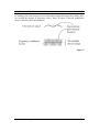
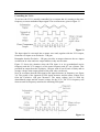
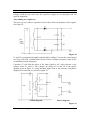
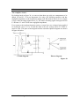
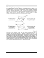
1
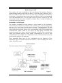
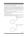
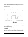
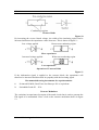
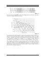
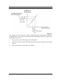
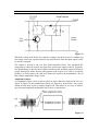
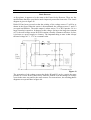
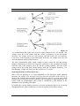
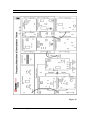
Frequency Modulation and
Demodulation Trainer
ST2203
Operating Manual
Ver 1.1
An ISO 9001 : 2000 company
94-101, Electronic Complex Pardesipura,
Indore- 452010, India
Tel : 91-731- 2570301/02, 4211100
Fax: 91- 731- 2555643
e mail : [email protected]
Website : www.scientech.bz
Toll free : 1800-103-5050
ST2203
Scientech Technologies Pvt. Ltd.
2
ST2203
Frequency Modulation and Demodulation Trainer
ST2203
Table of Contents
1.
2.
3.
4.
5.
6.
7.
8.
9.
Features
Technical Specifications
Frequency Components of Human Voice
A Simple Communication System
Advantage of FM
Disadvantage of FM
FM Transmitter
Varactor Modulator
• Experiment 1
Study of Frequency Modulation using Varactor modulator
Reactance Modulator
4
5
6
7
9
10
10
13
17
•
22
20
10.
Experiment 2
Study of Frequency Modulation Using Reactance Modulator
Demodulation of FM signal
25
11.
Detuned Resonant Circuit Detector
27
•
29
12.
13.
14.
15.
Experiment 3
Study of Operation of Detuned Resonant Circuit
Quadrature Detector
35
•
37
Experiment 4
Study of Operation of Quadrature Detector
Phase Locked Loop Detector
42
•
44
Experiment 5
Study of Operation of Phase-Locked Loop Detector
Foster Seeley Detector
47
•
51
Experiment 6
Study of Operation of Foster - Seeley Detector
Ratio Detector
54
•
56
Experiment 7
Study of Operation of Ratio Detector
16.
Coil Adjustment
59
17.
Switched Faults
62
18.
Warranty
63
19.
List of Accessories
63
Scientech Technologies Pvt. Ltd.
3
ST2203
Features
•
A self contained trainer.
•
Functional blocks indicated on board mimic.
•
Input - Output and Test points provided onboard.
•
Built-in DC power supply.
•
Fully documented student operating manual & work book.
•
8 switched faults.
•
On board audio, modulators, detectors, amplitude limiter & filter circuits.
•
Effect of noise on the detection of FM signal may be investigated.
•
Compact size.
Scientech Technologies Pvt. Ltd.
4
ST2203
Technical Specifications
Audio Oscillator
:
With adjustable amplitude & frequency
(300 Hz - 3.4 KHz)
Two Types of FM Modulator
:
1. Reactance Modulator
(with carrier frequency adjustment)
2. Varactor Modulator
(with carrier frequency adjustment)
Mixer / Amplifier
:
Allows FM input signal to be amplitude
modulated by a noise input prior to
demodulation, with gain adjustment.
Transmitter Output Frequency.
:
455 KHz
Five Types of FM Demodulator
:
1.
2.
3.
4.
5.
Low Pass Filter Amplifier
:
3.4 KHz cut off frequency.
(with adjustable gain)
Amplitude Limiter
:
1 No.
Switched Faults
:
8 Nos.
Power Supply
:
230 V ± 10%, 50Hz
Test Points
:
74 Nos.
Power Consumption
:
3VA (approximately)
Interconnections
:
4 mm Banana sockets
Dimensions (mm)
:
W420 x H100 x D255
Weight
:
3 Kgs. (approximately)
Scientech Technologies Pvt. Ltd.
Detuned Resonant Detector
Quadrature Detector
Foster - Seeley Detector
Ratio - Detector
Phase Locked Loop Detector
5
ST2203
Frequency Components of the Human Voice
When we speak, we generate a sound that is very complex and changes continuously
so that at a particular instant of time the waveform may appear as shown in figure 1
below.
Figure 1
However complicated the waveform looks, we can show that it is made of many
different sinusoidal signals added together. To record this information we have a
choice of three methods. The first is to show the original waveform as we did in
figure 1.
The second method is to make a list of all the separate sinusoidal waveforms that were
contained within the complex waveform (these are called 'components' or frequency
components). This can be seen in figure 2.
Figure 2
The third way is to display all the information on a diagram. Such a figure shows the
frequency spectrum. It is graph with amplitude plotted against frequency. A single
vertical line, the length of which, represents each separate frequency.
Represents the amplitude of the sine wave. Such a diagram is shown in figure 3. Note
that nearly all speech information is contained within the frequency range of 300Hz to
304 KHz.
Scientech Technologies Pvt. Ltd.
6
ST2203
Figure 3
Although an Oscilloscope will only show the original complex waveform, it is
important for us to remember that we are really dealing with a group of sine waves of
differing frequencies, amplitudes and phases.
A Simple Communication System
Once we are out of shouting range from another person, we must rely on some
communication system to enable us to pass information. The only essential parts of
any communication system are a transmitter, a communication link and a receiver,
and in the case of speech, this can be achieved by a length of cable with a microphone
and an amplifier at one end and a loudspeaker and an amplifier at the other.
Simple Communication System
Figure 4
For long distances, or when it is required to send signals to many destinations at the
same time, it is convenient to use a radio communication system. One of the
alternative systems is frequency modulation in which the information signal is used to
control the frequency of the carrier wave. This works equally well, and in some
respects, better than the amplitude modulation.
The frequency of the carrier is made to increase as the voltage in the information
signal increases and to decrease in frequency as it reduces. The larger the amplitude
of the information signal, the further the frequency of the carrier signal is shifted from
Scientech Technologies Pvt. Ltd.
7
ST2203
its starting point. The frequency of the information signal determines how many times
in a second this change in frequency occurs. Notice in figure 5 that the modulation
process does not affect the amplitude.
Figure 5
Scientech Technologies Pvt. Ltd.
8
ST2203
Advantages of FM
There are three advantages of frequency modulation for a communication system.
Electrical noise alters the amplitude but not the signal frequency
Figure 6
1.
In the last section, we saw that the information signal controlled the frequency
of the carrier but had no effect on its amplitude. Now, when any transmission is
affected by electrical noise, the noise signal is superimposed on the transmitted
signal as shown in figure 6 below.
In an AM System, the demodulator is designed to respond to changes in
amplitude of the received signal but in a FM receiver the demodulator is only
watching for changes in frequency and therefore ignores any changes in
amplitude. Electrical noise thus has little or no effect on a FM communication
system.
2.
The bandwidth of the FM signal is very wide compared with an AM
transmission. Typical broadcast bandwidths are in the order of 250 KHz. This
allows a much better sound quality, so signals like music sound significantly
better if frequency modulation is being used.
3.
When an FM demodulator is receiving an FM signal, it follows the variations in
frequency of the incoming signal and is said to lock on to the received at the
same time. The receiver 'lock on' to the stronger of the two signals and ignores
the other. This is called the 'capture effect' and it means that we can listen to an
FM station on a radio without interference from other stations.
Scientech Technologies Pvt. Ltd.
9
ST2203
Disadvantages of FM
This requires the wide bandwidth of the transmission. The medium frequency
broadcast band extends from about 550 KHz to 1,600 KHz, and is therefore only a
little over 1MHz in width. If we tried to use FM using a bandwidth of 250 KHz for
each station, it would mean that no more than four stations could be accommodated.
This wide bandwidth forces us to use higher carrier frequencies, usually in the VHF
band, which extends from about 85 MHz to 110MHz. This is a width of 25MHz and
would hold many more stations.
Bandwidth of an FM Signal :
The frequency modulation process generates a large number of side frequencies.
Theoretically the sidebands are infinitely wide with the power levels becoming lower
and lower as we move away from the carrier frequency. The bandwidth of 250 KHz
was chosen as a convenient value to ensure a low value of distortion in the received
signal whilst allowing many stations to be accommodated in the VHF broadcast band
Communication signals, which do not require the high quality associated with
broadcast stations can, adopt a narrower bandwidth to enable more transmissions
within their allotted frequency band. Marine communications for ship to ship
communications, for example, use a bandwidth of only 25 KHz but this is only for
speech and the quality is not important.
These bandwidth figure bear no easy relationship with the frequency of the
information signal or with the frequency deviation or, it seems anything else. FM is
unlike AM in this respect.
FM Transmitter
The block diagram is shown in figure 7 below.
FM Transmitter
Scientech Technologies Pvt. Ltd.
Figure 7
10
ST2203
The audio oscillator supplies the information signal and could, if we wish, can be
replaced by a microphone and AF amplifier to provide speech and music instead of
the sine wave signals that we are using with ST2203.
The FM modulator is used to combine the carrier wave and the information signal
much in the same way as in the AM transmitter. The only difference in this case is
that the generation of the carrier wave and the modulation process is carried out in the
same block. It is not necessary to have the two processes in same block, but in our
case, it is. The output amplifier increases the power in the signal before it is applied to
the antenna for transmission just as it did in the corresponding block in the FM
transmitter.
The only real difference between the AM and FM transmitters are the modulations, so
we are only going to consider this part of the transmitter.
We are going to investigate two types of modulator; they are called the varactor
modulator and the reactance modulator.
How do this modulators work?
The basic idea is quite simple and both modulations function in the same way. They
both include a RF oscillator to generate the carrier and these oscillators employ a
parallel tuned circuit to determine the frequency of operation.
The frequency of resonance
depends on the value of the
inductance and capacitance
This extra capacitance will
reduce
the
frequency
of
resonance
Figure 8
Scientech Technologies Pvt. Ltd.
11
ST2203
Adding an additional capacitor in parallel will cause the total capacitance to increase
and this will result in a decrease in the resonance frequency.
If you feel that a reminder of the formula may be helpful, the approximate frequency
of resonance is given by :
1
f=
Hz
2π LC
Where L is the inductance in Henrys and C is the capacitance in Farads
The tuned circuit is part of the oscillator used to generate the carrier frequency so, the
capacitance changes then so will the carrier frequency. This is demonstrated in figure
9.
Figure 9
To produce a frequency modulated carrier, all we have to do is to find a way of
making the information signal increase and decrease the size of the capacitance and
hence control the carrier frequency.
In the following sections we will look to see two ways of achieving this. First by
using a device called a varactor diode and then by using a transistor.
Varactor Diode :
The varactor diode is a semiconductor diode that is designed to behave as a voltage
controlled capacitor. When a semiconductor diode is reverse biased, no current flows
and it consists of two conducting regions separated by non-conducting region. This is
very similar to the construction of a capacitor.
Scientech Technologies Pvt. Ltd.
12
ST2203
Varactor Diode
Figure 10
By increasing the reverse biased voltage, the width of the insulating region can be
increased and hence the capacitance value decreases. This is shown in figure 11.
Low voltage applied
Narrow non-conducting region
More capacitance
Increased voltage applied
Wider non-conducting region
Less capacitance
Operation of Varactor Diode
Figure 11
If the information signal is applied to the varactor diode, the capacitance will
therefore be increased and decreased in sympathy with the incoming signal.
Recommended testing instruments for experimentation
1.
Scientech 20 MHz, Dual Trace Oscilloscope 201 or equivalent.
2.
Switchable Probe X1 – X10.
Varactor Modulator
The variations in capacitance form part of the tuned circuit that is used to generate the
FM signal to be transmitted. Have a look at the varactor modulator shown in figure
12.
Scientech Technologies Pvt. Ltd.
13
ST2203
Figure 12
We can see the tuned circuit which sets the operating frequency of the oscillator and
the varactor which is effectively in parallel with the tuned circuit. Two other
components which may not be immediately obvious are C1 and L1. C1 is a DC
blocking capacitor to provide DC isolation between the oscillator and the collector of
the transmitter. L1 is an RF choke which allows the information signal to pass
through the varactor but blocks the RF signals.
The operation of the varactor modulator :
1.
The information signal is applied to the base of the input transistor and appears
amplified and inverted at the collector.
2.
This low frequency signal passes through the RF choke and is applied across the
varactor diode.
3.
The varactor diode changes its capacitance in according to the information
signal and therefore changes the total value of the capacitance in the tuned
circuit.
4.
The changing value of capacitance causes the oscillator frequency to increase
and decrease under the control of the information signal. The output is therefore
a FM signal.
Before we start the study of varactor/ reactance modulation techniques we shall study
a simple VCO circuit.
Simply connect the audio output to the socket labeled VCO modulation in and
observe the FM modulated waveform on the Oscilloscope at the VCO modulation out
terminal. Keep the amplitude of audio output to approximately 4 V pp and frequency
2 KHz approximately Observe a stable FM modulated waveform on CRO.
This should look like as under. Similar waveforms are shown in Kennedy’s book.
Scientech Technologies Pvt. Ltd.
14
ST2203
Figure 13
Now turn the time base speed of CRO little higher and you will observe the same
waveforms as under (like Bessel function).
Figure 14
Now disconnect the audio amplifier's output from modulation In and connect it to
audio In, keep the reactance/varactor switch in varactor position. Observe the output
of mixer / amplifier circuit. Keep the Oscilloscope in X10 position now observe the
full waveform by shifting the X position. It is as shown in figure Mark the
resemblance between the output of VCO and the Varactor modulator. They are same.
The Frequency modulation in VCO was more because the Frequency difference
between the carrier and the modulating signal was very less. But in real life
applications reactance and varactor modulation techniques are used which utilizes
high frequency carrier and you will not observe signal as shown in figure 14 above,
but you will see as shown in figure 16.
Scientech Technologies Pvt. Ltd.
15
ST2203
Figure 15
Mind you both are frequency modulation and there should be no ambiguity about this.
The above is purposely included to make the students clearer in mind that the
varactor and reactance modulators used in this trainer are frequency modulators
only.
We shall now start experiment with varactor modulator.
Scientech Technologies Pvt. Ltd.
16
ST2203
Experiment 1
Objective :
Study of Frequency Modulation using Varactor modulator
Procedure :
This experiment investigates how ST2203's varactor modulator circuit performs
frequency modulation. This circuit modulates the frequency of a carrier sine wave,
according to the audio signal applied to its modulating input.
1.
Ensure that the following initial conditions exist on the ST2202 board.
a. All Switched Faults in ‘Off’ condition.
b. Amplitude potentiometer (in mixer amplifier block) in fully clockwise
position.
c. VCO switch (in phase locked loop detector block) in ‘Off’ position.
2.
Make the connections as shown in figure 13.
3.
Switch On the power.
4.
Turn the audio oscillator block's amplitude potentiometer to its fully clockwise
position, and examine the block's output TP1 on an Oscilloscope. This is the
audio frequency sine wave, which will be used as our modulating signal. Note
that the sine wave's frequency can be adjusted from about 300Hz to
approximately 3.4 KHz, by adjusting the audio oscillator's frequency
potentiometer.
Note also that the amplitude of this modulating signal is adjusted by audio
oscillator amplitude potentiometer Leave the amplitude potentiometer in
minimum position.
5.
Connect the output socket of the audio oscillator block to the audio input socket
of the modulator circuit’s block.
6.
Set the reactance / varactor switch to the varactor position. This switch selects
the varactor modulator and also disables the reactance modulator to prevent any
interference between the two circuits.
7.
The output signal from the varactor modulator block appears at TP24 before
being buffered and amplified by the mixer/amplifier block, any capacitive
loading (e.g. due to Oscilloscope probe) may slightly affect the modulators
output frequency. In order to avoid this problem we monitor the buffered FM
output signal the mixer / amplifier block at TP34.
8.
Put the varactor modulator's carrier frequency potentiometer in its midway
position, and then examine TP34. Note that it is a sine wave of approximately
1.2 Vpp, centered on 0V. This is our FM carrier, and it is un-modulated since
the varactor modulators audio input signal has zero amplitude.
Scientech Technologies Pvt. Ltd.
17
ST2203
9.
The amplitude of the FM carrier (at TP34) is adjustable by means of the
mixer/amplifier block's amplitude potentiometer, from zero to its potentiometer
level. Try turning this potentiometer slowly anticlockwise, and note that the
amplitude of the FM signal can be reduced to zero. Return the amplitude
potentiometer to its fully clockwise position.
10.
Try varying the carrier frequency potentiometer and observe the effects.
11.
Also, see the effects of varying the amplitude and frequency potentiometer in
the audio oscillator block.
12.
Turn the carrier frequency potentiometer in the varactor modulator block slowly
clockwise and note that in addition to the carrier frequency increasing there is a
decrease in the amount of frequency deviation that is present.
13.
Return the carrier frequency potentiometer to its midway position, and monitor
the audio input (at TP6) and the FM output (at TP34) triggering the
Oscilloscope on the audio input signal. Turn the audio oscillator's amplitude
potentiometer throughout its range of adjustment, and note that the amplitude of
the FM output signal does not change. This is because the audio information is
contained entirely in the signals frequency and not in its amplitude.
14.
By using the optional audio input module ST2108 the human voice can be used
as the audio modulating signal, instead of using ST2203's audio oscillator
block. If you have an audio input module, connect the module's output to the
audio input socket in the modulator circuit’s block. The input signal to the audio
input module may be taken from an external microphone be (supplied with the
module) or from a cassette recorder, by choosing the appropriate switch setting
on the module. Consult the user manual for the audio input module, for further
details.
Scientech Technologies Pvt. Ltd.
18
ST2203
Figure 16
Scientech Technologies Pvt. Ltd.
19
ST2203
Reactance Modulator
Figure 17 shows a complete reactance modulator.
Figure 17
In figure 17, the left hand half is the previous varactor modulator simply an oscillator
and a tuned circuit, which generates the un-modulated carrier. The capacitor C and the
resistor R are the two components used for the phase shifting, and together with the
transistor, form the voltage controlled capacitor. This voltage-controlled capacitor is
actually in parallel with the tuned circuit. This is not easy to see but figure 18 may be
helpful.
In the first part of the figure the capacitor and associated components have been
replaced by the variable capacitor, shown dotted.
In the next part, the two supply lines are connected together. We can justify this by
saying that the output of the DC power supply always includes a large smoothing
capacitor to keep the DC voltages at a steady value.
Scientech Technologies Pvt. Ltd.
20
ST2203
Figure 18
This large capacitor will have a very low reactance at the frequencies being used in
the circuit less than a milliohm. We can safely ignore this and so the two supply lines
can be assumed to be joined together. Remember that this does not affect the DC
potentials, which remain at the normal supply voltages.
If the two supply voltages are at the same AC potential, the actual points of
connection do not matter and so we can redraw the circuit as shown in the third part.
Operation of the Reactance Modulator :
If required, reference can be made to figure 17.
1.
The oscillator and tuned circuit provide the un-modulated carrier frequency and
this frequency is present on the collector of the transistor.
2.
The capacitor and the resistor provide the 90° phase shift between the collector
voltage and current. This makes the circuit appear as a capacitor.
3.
The changing information signal being applied to the base has the same effect
as changing the bias voltage applied to the transistor and, this would have the
effect of increasing and decreasing the value of this capacitance.
4.
As the capacitance is effectively in parallel with the tuned circuit the variations
in value will cause the frequency of resonance to change and hence the carrier
frequency will be varied in sympathy with the information signal input.
Scientech Technologies Pvt. Ltd.
21
ST2203
Experiment 2
Objective :
Study of Frequency Modulation Using Reactance Modulator
Procedure :
This experiment investigates how ST2203's reactance modulator circuit performs
frequency modulation. This circuit modulates the frequency of a carrier sine wave,
according to the audio signal applied to its modulating output. To avoid unnecessary
loading of monitored signals, X10 Oscilloscope probes should be used throughout this
experiment.
1.
Ensure that the following initial conditions exist on the ST2203 Module.
a. All Switch Faults in ‘Off’ condition.
b. Amplitude potentiometer (in the mixer/amplifier block) in fully clockwise.
c. VCO switch (in phase-locked loop detector block) in ‘Off’ position.
2.
Make the connections as shown in figure 19.
3.
Turn on power to the ST2203 module
4.
Turn the audio oscillator block's amplitude potentiometer to its fully clockwise
(Maximum) positions, and examines the block's output (TP1) on an
Oscilloscope.
This is the audio frequency sine wave, which will be used as our modulating
signal. Note that the sine wave's frequency can be adjusted from about 300 Hz
to approximately 3.4 KHz by adjusting the audio oscillator's frequency
potentiometer Note also that the amplitude of this audio modulating signal can
be reduced to zero, by turning the audio oscillator's amplitude potentiometer to
its fully counter clockwise position.
5.
Connect the output socket of the audio oscillator block to the audio input socket
of the modulator circuit’s block, as shown in figure 19.
6.
Put the reactance /varactor switch in the reactance position. This switches the
output of the reactance modulator through to the input of the mixer/amplifier
block~ and also switches off the varactor modulator block to avoid interference
between the two modulators.
7.
The output signal from the reactance modulator block appears at TP13, before
being buffered and amplified by the mixer/amplifier block. Although the output
from the reactance modulator block can be monitored directly at TP13, any
capacitive loading affect this point (e.g. due to an Oscilloscope probe) may
slightly affect the modulator's output frequency.
In order to avoid this problem we will monitor the buffered FM output signal
from the mixer/amplifier block at TP34.
8.
Put the reactance modulator's potentiometer in its midway position (arrow
pointing towards top of PCB) then examine TP34.
Scientech Technologies Pvt. Ltd.
22
ST2203
Note : that the monitored signal is a sine wave of approximately 1.2Vpp
centered on 0 volts DC This is our FM carrier, and it is presently un-modulated
since the reactance modulator's audio input signal has, zero amplitude.
9.
The amplitude of the FM carrier (at TP34) is adjustable by means of the
mixer/amplifier block's amplitude potentiometer, from zero to its present level.
Try turning this potentiometer slowly anticlockwise, and note that the amplitude
of the FM signal can be reduced to zero.
Return the amplitude potentiometer to its fully clockwise position.
10.
The frequency of the FM carrier signal (at TP34) should be approximately 455
KHz at the moment This carrier frequency can be varied from 453 KHz to 460
KHz (approximately) by adjusting the carrier frequency potentiometer in the
reactance modulator block.
Turn this potentiometer over its range of adjustment and note that the frequency
of the monitored signal can be seen to vary slightly. Note also that the carrier
frequency is maximum when the potentiometer is in fully clockwise position.
11.
Try varying the amplitude & frequency potentiometer in audio oscillators block,
and also sees the effect of varying the carrier frequency potentiometer in the
mixer/amplifiers block.
12.
Monitor the audio input (at TP6) and the FM output (at TP34) triggering the
Oscilloscope on the audio input signal. Turn the audio oscillator's amplitude
potentiometer throughout its range of adjustment and note that the amplitude of
the FM output signal does not change. This is because the audio information is
contained entirely in the signal's frequency, and not in its amplitude.
13.
The complete circuit diagram for the reactance modulator is given at the end of
operating manual. If you wish, follow this circuit diagram and examine the test
points in the reactance modulator block, to make sure that you fully understand
how the circuit is working.
14.
By using the optional audio input module, the human voice can be used as the
audio modulating signal, instead of using ST2203’s audio oscillator block.
If you have an audio input module, connect the module's output to the audio
input socket in the modulator circuit’s block
The input signal to the audio input module may be taken from an external
microphone (supplied with the module), or from a cassette recorder, by
choosing the appropriate switch setting on the modules.
Scientech Technologies Pvt. Ltd.
23
ST2203
Figure 19
Scientech Technologies Pvt. Ltd.
24
ST2203
Demodulation on FM Signals
A FM receiver is very similar to an AM receiver. The most significant change is that
the demodulator must now extract the information signal from a frequency rather than
amplitude modulated wave.
FM Receiver
Figure 20
The basic requirement of any FM demodulator is therefore to convert frequency
change into change in voltage, with the minimum amount of distortion. To achieve
this, it should ideally have a linear voltage/frequency characteristic, similar to that
shown in figure 21. A demodulator can also be called a 'discriminator' or a 'detector'.
Scientech Technologies Pvt. Ltd.
25
ST2203
Figure 21
Any design of circuit that has a linear voltage/frequency characteristic would be
acceptable and we are point to consider the five most popular types. In each case the
main points to look are :
•
How do they convert FM signals into AM signals?
•
How linear is their response-this determines the amount of distortion in the final
output.
•
How good are they at rejecting noise signals?
Scientech Technologies Pvt. Ltd.
26
ST2203
Detuned Resonant Circuit Detector
This is the simplest form of demodulator. It works-but it does have a few drawbacks.
A parallel tuned circuit is deliberately detuned so that the incoming carrier occurs
approximately halfway up the left-hand slope of the response.
Figure 22
In figure 22 above, we can see that the amplitude of the output signal will increase
and decrease as the input frequency changes. For example, if the frequency of the
incoming signal were to increase, the operating point would move towards the right
on the diagram. This would cause an increase in the amplitude of the output signal.
A FM signal will therefore result in an amplitude-modulated signal at the output it is
really that simple! Figure 23 below shows the circuit diagram of the detuned resonant
circuit detector.
If we break it down, the operation becomes very clear. The FM input is applied to the
base of the transistor and in the collector there is the detuned resonant circuit that we
have met earlier. In reality, it also includes the loading effect caused by the other
winding which acts as a transmitter secondly; the signal at the collector of the
transistor includes an amplitude modulated component, which is passed to the diode
detector. In the figure 23 the diode conducts every time the input signal applied to its
anode is more positive than the voltage on the top plate of the capacitor.
Scientech Technologies Pvt. Ltd.
27
ST2203
Figure 23
When the voltage falls below the capacitor voltage, the diode ceases to conduct and
the voltage across the capacitor leaks away until the next time the input signal is able
to switch it on again.
The output is passed to the low Pass Filter/Amplifier block. The unwanted DC
component is removed and the low-pass filter removes the ripple at the IF frequency.
One disadvantage is that any noise spikes included in the incoming signal will also be
passed through the diode detector and appears at the output if we want to avoid this
problem, we must remove the AM noise before the input to the demodulator. We do
this with an Amplitude Limiter circuit.
Amplitude Limiter :
An Amplitude limiter circuit is able to place an upper and lower limit on the size of a
signal. In figure 24 the potentiometer limits are shown by dotted lines. Any signal,
which exceeds these levels, is simply chopped off. This makes it very easy to remove
any unwanted amplitude modulation due to noise or interference.
Figure 24
Scientech Technologies Pvt. Ltd.
28
ST2203
Experiment 3
Objective :
Study of Operation of Detuned Resonant Circuit
Procedure :
This experiment investigates how the detuned resonant circuit detector block on the
ST2203 module performs frequency demodulation. The operation of this detector
circuit will be described in detail, and its sensitivity to noise on the incoming FM
signal will be investigated.
The on-board amplitude limiter will then be used to remove any amplitude variations
due to noise, before they reach the detector. This allows the student to draw
conclusions as to whether it is necessary to precede this type of detector with an
amplitude limiter stage, in a practical FM receiver.
To avoid unnecessary loading of monitored signals, X10 Oscilloscope probes should
be used throughout this experiment.
1.
Ensure that the following initial conditions exist on the ST2203 module.
a.
All Switched Faults in ‘Off’ condition.
b.
Audio amplifier block's amplitude potentiometer in fully clockwise
(maximum) position.
c.
Audio amplifier block's frequency potentiometer in fully counterclockwise position.
d.
Amplitude potentiometer (in the mixer/amplifier block) in fully clockwise
position.
e.
VCO switch (in phase - locked loop detector block) in ‘Off’ position.
2.
Make the connections as shown in figure 25.
3.
Switch on the power to the ST2203 module.
4.
Initially, we will use the varactor modulator to generate our FM signal, since
this is the more linear of the two frequency modulators.
5.
To select the varactor modulator, put the reactance/varactor switch in the
varactor position.
Ensure that the varactor modulator's carrier frequency potentiometer is in the
midway position (arrowhead pointing towards top of PCB).
6.
The audio oscillator's output signal (which appears at TP1) is now being used
by the varactor modulator, to frequency'- modulate a 455 KHz carrier sine
wave. As we saw earlier, this FM waveform appears at the FM output socket
from the mixer/amplifier block.
You may like to examine this FM waveform at TP34. However, with the
varactor modulator's carrier frequency potentiometer in its present (midway)
position, the frequency deviation is quite small. To be able to notice such a
Scientech Technologies Pvt. Ltd.
29
ST2203
small frequency deviation, you will probably need to have a control on your
Oscilloscope.
If you have such a control, display 20-25 cycles of the waveform on the
Oscilloscope, and then use the X-expansion control to 'expand up' the right most
cycles of the display. There should be a slight ambiguity in the positions of
these cycles, indicating that the sine wave at TP34 is being frequencymodulated.
7.
Now monitor the audio input signal to the varactor modulator block (at TP14),
together with the output from the detuned resonant circuit block (at TP40)
triggering the Oscilloscope on TP14). The signal at TP40 should contain three
components :
•
A positive DC offset voltage;
•
A sine wave at the same frequency as the audio signal all TP14.
•
A high-frequency ripple component of small amplitude.
Check that the audio-frequency component is a reasonable sine wave. If it is
not, it is likely that the centre frequency of the varactor modulator's FM output
needs adjusting slightly. To do this, trim transformer T2 in the varactor
modulator block, in accordance with the instructions given in chapter.
(Adjustment of ST2203's tuned circuits).
8.
The low-pass filter/amplifier block strongly attenuates the high frequency ripple
component at the detector's output, and also blocks the DC offset voltage.
Consequently, the signal at the output of the low-pass filter/amplifier block (at
TP73) should very closely resemble the original audio modulating signal.
Monitor the input (TP69) and output (TP73) of the low pass filter/amplifier
block (triggering on TP 73) and note how the quality of the detector's output
signal has been improved by low pass filtering. Note also that the DC offset has
been removed.
9.
Monitor the audio input to the varactor modulator (at TP14) and the output of
the low-pass filter/amplifier block (at TP73) and adjust the gain potentiometer
in the low pass filter/amplifier block, until the amplitudes of the two monitored
audio waveforms are the same.
10.
Adjust the audio oscillator block's amplitude and frequency potentiometer, and
compare the original audio signal with the final demodulated signal. You may
notice that the demodulated output suffers attenuation as the audio modulating
frequency is increased. This is caused by low-pass filtering, which takes place
in the detuned resonant circuit's envelope detector, and in the low pass
filter/amplifier block.
In spite of this high-frequency limitation to the range of audio frequencies,
which can be received, the bandwidth of the system is perfectly adequate for
normal speech communication.
Scientech Technologies Pvt. Ltd.
30
ST2203
In the audio oscillator block, put the amplitude potentiometer in its maximum
position, and the frequency potentiometer in its Minimum position.
11.
We will now investigate the effect of noise on the system. Adjust the external
signal generator for a sinusoidal output of amplitude 100m Vpp, and frequency
2 KHz; this will be our 'noise' input. Connect the output of the signal generator
to the noise input socket in ST2203's modulator circuit’s block. Then, monitor
the noise input (at TP5) and the FM output (at TP34) triggering the
Oscilloscope on TP5. Note that the FM signal is now being amplitudemodulated by the 'noise' input, in addition to being frequency-modulated by the
audio input from the audio oscillator block. The amplitude modulations
simulate the effect that transmission path noise would have on the amplitude of
the FM waveform reaching the receiver. This allows us to investigate the effect
of transmission path noise would have on the final demodulated audio signal.
12.
Monitor the audio modulating signal (at TP14) and the output of the low pass
filter/amplifier block (at TP73), triggering the Oscilloscope from TP14.
Note that there is now an additional component at TP73a sine wave at the
frequency of the 'noise' input. To see this clearly, it may be necessary to slightly
adjust the frequency of the signal generator's output, until the superimposed
'noise' sine wave can be clearly seen.
13.
Remove the Oscilloscope probe form TP73, and place it on TP40, the output
form the detuned resonant circuit detector. Note that the 'noise' component is
still present, illustrating that this type of detector is very susceptive to amplitude
variations in the incoming FM signal.
Put the Oscilloscope probe on TP39 (the collector of the detuned resonant
circuit's transistor) to ensure that you fully understand why this type of detector
is so sensitive to amplitude variations.
14.
Turn the audio oscillator block's amplitude potentiometer to its minimum
position, so that no frequency modulation takes place. Then monitor the 'noise'
input (at TP5) and the output from the low pass filter/amplifier block (at TP73),
triggering the Oscilloscope from TP5.
The signal at TP73 in now purely composed of the 'noise' output resulting from
amplitude variations occurring at the input to the detuned resonant circuit.
Measure and record the peak-to-peak amplitude of the 'noise' output at TP73;
this measurement will be valuable in allowing us to compare the detuned
resonant circuit with other types of FM detector, as far as susceptibility to
amplitude modulation is concerned.
15.
To overcome the problem of the detuned resonant circuit detector's
susceptibility to noise, we can connect an amplitude limiter block between the
FM output and the input to the detuned resonant circuit. The amplitude limiter
removes amplitude variations from the FM output signal, so that the input signal
to the detuned resonant circuit detector has constant amplitude. Reconnect the
Scientech Technologies Pvt. Ltd.
31
ST2203
amplitude limiter block between the mixer/amplifier block and the detuned
resonant circuit block as shown in figure 26 at the end.
16.
Monitor the amplitude limiter's output at TP68, triggering the Oscilloscope from
TP5, the noise input form the signal generator. Note that the amplitude
modulations due to the noise input have been removed.
Remove the Oscilloscope probe from TP68, and put it on TP73, the output form
the low pass filter/amplifier block. Note that the amplitude of any remaining
'noise' component at TP73 is now minimal.
17.
Return the audio oscillator blocks amplitude potentiometer to its maximum
position, and monitor TP73, triggering the Oscilloscope on the audio
modulating input at TP14.
Note that amplitudes now have no effect on the final audio output.
This shows how an amplitude limiter can be used in a practical FM receiver, to
remove amplitude variations caused by noise, before they reach the detector.
18.
19.
By using the optional audio input module and audio output module the human
voice can be used as the audio modulating signal, instead of using ST2203's
audio oscillator block. If you have these modules, make the following
connections :
•
Output of audio input module to audio input socket in ST2203's
modulator circuits block;
•
Output of ST2203's low pass filter/amplifier block to input socket of
audio output module.
•
Refer the user manuals for the audio input module ST2108 and audio
output module ST2109 for further details of how to use them.
Throughout this experiment, frequency modulation has been performed by
ST2203's varactor modulator block.
Equally, using the reactance modulator block may perform frequency
modulation. If you wish to repeat any of the above experimentation with the
reactance modulator, simply put the reactance/varactor switch in the reactance
position.
Note : However, that the linearity of the reactance modulator is not as good as
that of the varactor modulator. This means that, when the reactance modulator is
used, some distortion of the demodulated audio signal may be noticeable at the
detector's output, if the amplitude of the audio-modulating signal is too large.
20.
Finally, make sure that you fully understand the working of the detuned
resonant circuit detector by examining the circuit diagram for the detector at the
end of this manual, and monitoring Test Points within the circuit.
Scientech Technologies Pvt. Ltd.
32
ST2203
Figure 25
Scientech Technologies Pvt. Ltd.
33
ST2203
Figure 26
Scientech Technologies Pvt. Ltd.
34
ST2203
Quadrature Detector
This is another demodulator, again fairly simple but is an improvement over the
previous design. It causes less distortion and is also better, though not perfect, when it
comes to removing any superimposed noise. The incoming signal is passed through a
phase - shifting circuit. The degree of phase shift that occurs is determined by the
exact frequency of the signal at any particular instant. The rules for the degree of
phase shift are :
1.
If the carrier is un-modulated, the phase shift is 90°.
2.
If the carrier increases in frequency the phase shift is less than 90°.
3.
If the carrier decreases in frequency, the phase shift is greater than 90°.
We now only require a circuit which is capable detect the changes in the phase of the
signal.
A phase comparator circuit as shown in figure 27
Quadrature Detector
Figure 27
This circuit compares the phase of original input signal with the output of the phase
the comparison according to the following, rules;
1.
It provides no change in output voltage if the signal phase has been shifted to
90°.
2.
Phase over 90° result in an decreased DC voltage level.
3.
Phases less than 90° result in an increased DC voltage level.
As the phase changes, the DC voltage level moves up and down and re-creates the
audio signal.
A low pass filter is included to reduce the amplitude of any high-frequency ripple and
blocks the DC offset. Consequently, the signal at the output closely resembles the
original input signal.
The characteristic as shown in figure 28 is straight to cause very little distortion to the
final audio output.
Scientech Technologies Pvt. Ltd.
35
ST2203
Figure 28
Scientech Technologies Pvt. Ltd.
36
ST2203
Experiment 4
Objective :
Study of Operation of Quadrature Detector
Procedure :
This experiment investigates how the quadrature detector block on the ST2203
module performs frequency demodulation. The operation of this detector circuit will
be described in detail, and its sensitivity to noise on the incoming FM signal will be
investigated.
The on-board amplitude limiter will then be used to remove any amplitude
modulations due to noise, before they reach the detector. This allows the student to
draw conclusions as to whether it is necessary to precede this type of detector with an
amplitude limiter state, in a practical FM receiver. To avoid unnecessary loading of
monitored signals, X10 Oscilloscope probes should be used throughout this
experiment.
1.
Ensure that the following initial conditions exist on the ST2203 module.
a. All Switch Faults in ‘Off’ condition.
b. Audio amplifier block's amplitude potentiometer in fully clockwise
(maximum) position;
c. Audio oscillator block's frequency potentiometer in fully counter clockwise
(minimum) position.
d. Amplitude present (in the mixer/amplifier block) in fully clockwise position.
e. VCO switch (in phase-locked loop detector block) in ‘Off’ position.
2.
Make the connections shown in figure 29.
3.
Turn on power to the ST2203 module.
4.
Initially, we will use the varactor modulator to generate our FM signal, since
this is the more linear of the two frequency modulators as far as its
frequency/voltage characteristic is concerned.
To select the varactor modulator, put the reactance/varactor switch in the
varactor position.
Ensure that the varactor modulator's carrier frequency potentiometer is in the
midway position.
The varactor modulator, to frequency-modulate a 455 KHz-carrier sine wave is
now using the audio oscillator's output signal (which appears at TP1). As we
saw earlier, this FM waveform appears at the FM output socket from the mixer/
amplifier block. You will probably need to have an X-expansion control on
your Oscilloscope.
Now monitor audio input signal to the varactor modulator block (at TP14)
together with the output form the quadrature detector block (at TP46), triggering
the Oscilloscope. The signal at TP46 should contain three components.
5.
6.
Scientech Technologies Pvt. Ltd.
37
ST2203
a. A positive DC offset voltage.
b. A sine wave at the same frequency as the audio signal at TP14.
c. A high-frequency ripple component of small amplitude.
Check that the audio frequency component is a reasonable sine wave. It is likely
that the entire frequency of the varactor modulator's FM output needs right
adjustment. To do this, trim transformer T2 in the varactor modulator block, in
accordance with the instructions given in chapter coil adjustments.
7.
The low-pass filter/amplifier block strongly attenuates the high frequency ripple
component at the detector's output, and also blocks the DC offset voltage.
Consequently, the signal at the output of the low-pass filter/amplifier block (at
TP73) should very closely resemble the original audio modulating signal.
8.
Monitor the audio input to the varactor modulator (at TP14) and the output of
the low-pass filter/amplifier block (at TP73) and adjust the gain potentiometer
(in the low pass filter/amplifier block) until the amplitudes of the monitored
audio waveforms are the same.
9.
Adjust the audio oscillator block's amplitude and frequency potentiometer and
compare the original audio signal with the final demodulated signal.
10.
We will now investigate the effect of noise on the system.
Adjust the signal generator for a sinusoidal output of amplitude 100m Vpp, and
frequency 2 KHz, this will be our 'noise' input.
Connect the output of the signal generator to the noise input socket in ST2203's
modulator circuit’s block. Monitor the noise input (at TP5) and the FM output
(at TP34) triggering the Oscilloscope on TP5.
Note that the FM signal is now being amplitude-modulated by the 'noise' input,
in addition to being frequency-modulated by the audio input from the audio
oscillator block.
The amplitude modulations simulate the effect that transmission path noise
would have on the amplitude of the FM waveform reaching the receiver. This
allows us to demodulated audio signal.
11.
Monitor the audio modulating signal (at TP14) and the output of the low pass
filter/amplifier block (at TP73), triggering the Oscilloscope from TP14.
12.
Remove the Oscilloscope probe form TP73 and place it on TP46 the output
form the quadrature detector block. Note that the small 'noise' component is still
visible.
13.
Turn the audio oscillator block's amplitude potentiometer to its MIN position,
so that no frequency modulation takes place. Then monitor the 'noise' input (at
TP5) and the output from the low pass filter/amplifier block (at TP73, triggering
the Oscilloscope from TP5.
Scientech Technologies Pvt. Ltd.
38
ST2203
14.
To reduce the effect of amplitude variations even further, we can connect an
amplitude limiter block between the FM output and the input to the quadrature
detector.
The amplitude limiter removes amplitude variations from the FM output signal,
so that the input signal to the quadrature detector has constant amplitude.
Reconnect the amplitude limiter block between the mixer/amplifier block and
the quadrature detector block, as shown in figure 30.
15.
Monitor the amplitude limiter's output at TP68, triggering the Oscilloscope from
TP5, the 'noise' input from the signal generator. Note that the amplitude
modulations due to the 'noise' input have been removed.
Remove the Oscilloscope probe from TP68, and put it on TP73, the output form
the low pass filter/amplifier block. Note that the amplitude of any remaining
'noise' component at TP73 is now minimal.
16.
By using the optional audio input module and audio output module, the human
voice can be used as the audio modulating signal, instead of using ST2203's
audio oscillator block.
17.
Throughout this experiment, frequency modulation has been performed by
ST2203's varactor modulator block. Using the reactance modulator block we
may perform frequency modulation.
Scientech Technologies Pvt. Ltd.
39
ST2203
Figure 29
Scientech Technologies Pvt. Ltd.
40
ST2203
Figure 30
Scientech Technologies Pvt. Ltd.
41
ST2203
Phase Locked Loop Detector
This is another demodulator that employs a phase comparator circuit. It is a very good
demodulator and has the advantage that it is available, as a self-contained integrated
circuit so there is no set up required. You plug it in and in works. For these reasons, it
is often used in commercial broadcast receivers. It has very low levels of distortion
and is almost immune from external noise signals and provides very low levels of
distortion. Altogether a very nice circuit.
Phase Lock Loop Detector
Figure 31
The overall action of the circuit may, at first, seem rather pointless. As we can see in
Figure 31, there is a Voltage-Controlled Oscillator (VCO). The DC output voltage
from the output of the low pass filters controls the frequency of this oscillator. Now
this DC voltage keeps the oscillator running at the same frequency as the original
input signal and 90° out of phase. And if we did, then why not just add a phase
shifting circuit at the input to give the 90° phase shift? The answer can be seen by
imagining what happens when the input frequency changes - as it would with a FM
signal. If the input frequency increases and decreases, the VCO frequency is made to
follow it. To do this, the input control voltage must increase and decrease. These
change of DC voltage level that forms the demodulated signal. The AM signal then
passes through a signal buffer to prevent any loading effects from disturbing the VCO
and then through an audio amplifier if necessary. The frequency response is highly
linear as shown in figure 32.
Figure 32
Scientech Technologies Pvt. Ltd.
42
ST2203
Controlling the VCO :
To see how the VCO is actually controlled, let us assume that it is running at the same
frequency as an un-modulated input signal. The waveforms are given in figure 33.
Figure 33
The input signal is converted into a square wave and, together with the VCO output,
forms the two inputs to an Exclusive - OR gate.
Remember that the Exclusive - OR gate provides an output whenever the two inputs
are different in value and zero output whenever they are the same.
Figure 33 shows the situation when the FM input is at its un-modulated carrier
frequency and the VCO output is of the same frequency and 900 out of phase. This
provided an output from the Exclusive -OR gate with an on-off ratio of unity and an
average voltage at the output of half of the peak value (as shown).
Now let us assume that the FM signal at the input decreases in frequency (see figure
34). The period of the 'squared up' FM signal increases and the mean voltage level
from the Exclusive -OR gate decreases. The mean voltage level is both the
demodulated output and the control voltage for the VCO. The VCO frequency will
decrease until its frequency matches the incoming FM signal.
Figure 34
Scientech Technologies Pvt. Ltd.
43
ST2203
Experiment 5
Objective :
Study of Operation of Phase-Locked Loop Detector
Procedure :
This experiment investigates how the phase-locked loop detector block on the
ST2203 module performs frequency demodulation. The operation of this detector
circuit will be described in detail and its sensitivity to noise on the incoming FM
signal will be investigated. On-board amplitude limiter will then used to remove any
amplitude modulations due to noise, before they reach the detector. This allows the
student to draw conclusions as to whether it is necessary to precede this type of
detector with an amplitude limiter stage, in a practical FM receiver.
To avoid unnecessary loading of monitored signals, X10 Oscilloscope probes should
be used throughout this experiment.
1.
Ensure that the following initial conditions exist on the ST2203 module:
a. All Switched Faults in ‘Off’ condition.
b. Audio amplifier block's amplitude potentiometer in fully clockwise
(maximum) position.
c. Audio amplifier block's frequency potentiometer in fully counter clockwise.
Ensure that the following initial conditions exist on the ST2203 clockwise
(minimum) position.
d. Amplitude potentiometer (in the mixer/amplifier block) in fully clockwise
position;
e. VCO switch (in phase-locked loop detector block) in ‘On’ position.
2.
Make the connections shown in figure 35.
3.
Turn on power to the ST2203 module.
4.
Now monitor the audio input signal to the varactor modulator block (at TP14)
together with the output from the phase-locked loop detector block (at TP60),
triggering the Oscilloscope in TP14. The signal at TP68 should contain three
components.
5.
•
A positive DC offset voltage.
•
A sine wave at the same frequency as the audio signal at TP14.
•
A high - frequency ripple component.
The low pass filter/amplifier block strongly attenuates the high-frequency ripple
component at the detector's output and also blocks the DC offset voltage.
Consequently the signal at the output of the low- pass filter/amplifier block (at
TP73) should be very closely resemble the original audio making signal, if not
then slowly adjust the frequency adjust potentiometer of PLL block.
Scientech Technologies Pvt. Ltd.
44
ST2203
6.
Adjust the audio oscillator block's amplitude and frequency potentiometer and
compare the original audio signal with the final demodulated signal.
7.
We can investigate the effect of noise on the system by following the procedure
given in earlier experiments. The only change will be that we will use phase
locked loop detector instead of quadrature or detuned resonant circuit.
Scientech Technologies Pvt. Ltd.
45
ST2203
Figure 35
Scientech Technologies Pvt. Ltd.
46
ST2203
Foster Seeley Detector
The last two demodulators to be considered employ the phase shift that often
accompanies a change in frequency in an AC circuit. The Foster Seeley circuit is
shown in figure 36. At first glance, it looks rather complicated but it becomes simpler
if we consider it a bit at a time.
Figure 36
When the input signal is un-modulated :
We will start by building up the circuit a little at a time. To do this, we can ignore
many of the companies. Figure 37 shows only the parts, which are in use when the
FM input signal is un-modulated.
Figure 37
We may recognize immediately that it consist of two envelope detectors like half
wave rectifiers being fed from the center-tapped coil L2. With reference to the centertap, the two voltages V1 and V2 are in anti-phase as shown by the arrows. The output
Scientech Technologies Pvt. Ltd.
47
ST2203
voltage would be zero volts since the capacitor voltages are in anti-phase and are
equal in magnitude.
After adding two capacitors :
The next step is to add two capacitors and see their effect on the phase of the signals.
See figure 38.
Figure 38
L1 and L2 are magnetically tightly coupled and by adding C3 across the centre-tapped
coil, they will form a parallel tuned circuit with a resonance frequency equal to the
un-modulated carrier frequency.
Capacitor C5 will shift the phase of the input signal by 90° with reference to the
voltage across L1 and L2. The voltages are shown as Va and Vb in the phasor
diagram given in figure 39. Using the input signal Vfm as the reference, the phasor
diagrams now look the way shown in figure 39.
Circuit diagram
Phasor diagram
Figure 39
Scientech Technologies Pvt. Ltd.
48
ST2203
The complete circuit :
By looking back at figure 36, we can see that there are only two components to be
added, C4 and L3. C4 is not important. It is only a DC blocking capacitor and has
negligible impedance at the frequencies being used. But what it has to do is to supply
a copy of the incoming signal across L3. The entire incoming signal is dropped across
L3 because C1 and C2 also have negligible impedance.
If we return to the envelope detector section, we now have two voltages being applied
to each diode. One is V1 or V2 and the other is the new voltage across L3, which is
equal to Vfm. This part of the diagram and the associated phasor diagram are shown
in figure 40 below.
Circuit diagram
Phasor diagram
Figure 40
Scientech Technologies Pvt. Ltd.
49
ST2203
When the input Frequency changes :
If the input frequency increased above its un-modulated value, the phasor of Va
would fall below 90° due to the parallel tuned circuit becoming increasingly
capacitive. The phasor representing V1 and V2 would move clockwise as shown in
figure 41. This would result in a larger total voltage being applied across D1 and a
reduced voltage across D2. Since the capacitor C1 would now charge to a higher
voltage, the final output from the circuit would be a positive voltage.
Figure 41
Conversely, if the frequency of the FM input signal decreased below the unmodulated value, the phase shift due to capacitor C5 increases above 90° as the
parallel tuned circuit becomes slightly inductive. This causes the voltage across diode
D2 to increase and the final output from the demodulator becomes negative. The
effect of noise is to change the amplitude of the incoming FM signal resulting in a
proportional increase and decrease in the amplitude of diode voltages VD1 and VD2
and the difference in voltage is the demodulated output, the circuit is susceptible to
noise interference and should be preceded by a noise limiter circuit.
Scientech Technologies Pvt. Ltd.
50
ST2203
Experiment 6
Objective :
Study of Operation of Foster - Seeley Detector
Procedure :
This experiment investigates how the Foster-Seeley detector on the ST2203 module
performs frequency demodulation. The operation of this detector circuit will be
described in detail and its sensitivity to noise on the incoming FM signal will be
investigated. The onboard amplitude limiter will then be used to remove any
amplitude modulations due to noise, before they reach the detector. This allows the
student to draw conclusions as to whether it is necessary to precede this type of
detector with an amplitude limiter state. In a practical FM receiver.
1.
Ensure that the following initial conditions exist on the ST2203 module:
a. All Switched Faults in ‘Off’ condition.
b. Audio amplifier block's amplitude potentiometer in fully clockwise
(maximum) position.
c. Audio amplifier block's frequency potentiometer in fully counter-clockwise
(minimum) position.
d. Amplitude potentiometer (in the mixer/amplifier block) in fully clockwise
position.
e. VCO switch (in phase-locked loop detector block) in ‘Off’ position.
2.
Make connection as shown in figure 42
3.
Turn on power to the ST2203 module.
4.
We will now investigate the operation of the Foster-Seeley detector on the
ST2203 module.
In the Foster-Seeley/ratio detector block, select the Foster-Seeley detector by
putting the switch in the Foster-Seeley position.
5.
Initially, we will use the varactor modulator to generate our FM signal, since
this is the more linear of the two modulators, as fast as its frequency/voltage
characteristic is concerned. To select the varactor modulator, put the reactance/
varactor switch in the varactor position.
Ensure that the varactor modulator's carrier frequency potentiometer is in the
midway position.
6.
The audio oscillator's output signal (which appears at TP1) is now being used
by the varactor modulator, to frequency-modulate a 455 KHz carrier sine wave.
As we saw earlier, this FM waveform appears at the FM output socket from the
mixer/amplifier block. You will probably need to have an X-expansion control
on your Oscilloscope.
Scientech Technologies Pvt. Ltd.
51
ST2203
7.
Now monitor the audio input signal to the varactor modulator block (at TP14)
together with the Foster-Seeley output from the Foster-Seeley/ratio detector
block (at TP52), triggering the Oscilloscope on TP14.
The signal at TP52 should contain two components :
•
A sine wave at the same frequency as the audio signal at TP14.
•
A High frequency ripple component of small amplitude.
8.
The Low-Pass Filter/amplifier strongly attenuates this high-frequency
component, and blocks any small DC offset voltage that might exist
detector's output. Consequently, the signal at the output of the Low-Pass
amplifier block (at TP73) should very closely resemble the original
modulating signal.
9.
Monitor the audio input to the varactor modulator (at TP14) and the output of
the Low Pass Filter/amplifier block (at TP73) and adjust the gain potentiometer
(in the Low Pass Filter/amplifier block) until the amplitudes of the monitored
audio waveforms are the same.
10.
Adjust the audio oscillator block's amplitude and frequency potentiometer, and
compare the original audio signal with the final demodulated signal.
11.
We can investigate the effect of noise on the system by following the procedure
given in earlier chapters by merely substituting quadrate detector by FosterSeeley Detector.
Scientech Technologies Pvt. Ltd.
ripple
at the
Filter/
audio
52
ST2203
Figure 42
Scientech Technologies Pvt. Ltd.
53
ST2203
Ratio Detector
At first glance, it appears to be the same as the Foster-Seeley Detector. There are few
modifications that have provided a much-improved protection from noise. The circuit
diagram is given in figure 43.
Diode D2 has been reversed so that the polarity of the voltage across C2 will be as
shown in the figure When the carrier is un-modulated; the voltages across C1 and C2
are equal and additive. The audio output is taken across C2 or R2 Capacitor C6 is a
large electrolytic capacitor. It charges to this voltage. Owing to the long time constant
of C6, the total voltage across R1 & R2 remains virtually constant at all times. In fact,
it just acts as a power supply or a battery. The important thing to note is that it keeps
the total voltage of C 1 +C 2 at a constant value.
Figure 43
The generation of the voltage across the diodes Dl and D2 are by exactly the same
process as we met in the Foster-Seeley Detector. Indeed even the changes in voltage
occur in the same way and for the same reasons. For convenience, the resulting phasor
diagrams are repeated here in figure 44.
Scientech Technologies Pvt. Ltd.
54
ST2203
Figure 44
An un-modulated FM signal will result in equal voltages across R1 and R2. The
voltage across R2 is the output from the circuit. If frequency of the FM signals
increases, the voltage across R1 will increase and that across R2 will decrease.
Conversely, if the frequency of the FM signals decreases, the voltage across R1 will
decrease and that across R2 will increase.
The final demodulated audio output voltage is taken across R2 and this voltage
changes continuously to follow the frequency variations of the incoming FM signal.
Since the sum of the voltages across R1 and R2 remains constant. The ratio of the
voltage across R2 to this total voltage changes with the FM signal's frequency. It is
this changing voltage ratio that gives the ratio detector its name.
Reducing the Effect of Electrical Noise :
This is the real purpose of C6. If the amplitude of the FM input signal suddenly
increases, the voltage VD1 and VD2 will try to increase and these in turn will try to
increase the voltages across both R1 and R2. However, since C6 is large, the overall
voltage across R1 and R2 will not respond to the fast change in input amplitude. The
result is that the demodulated audio output is unaffected by fast changes in the
amplitude of the incoming FM signal.
R3 and R4 are current limiting resistors to prevent momentary high levels of current
through the diodes, which would cause a brief fluctuation in the output voltage.
Scientech Technologies Pvt. Ltd.
55
ST2203
Experiment 7
Objective :
Study of Operation of Ratio Detector
Procedure :
This experiment investigates how the ratio detector on the ST2203 module performs
frequency demodulation. The operation of this detector circuit will be described in
detail and its sensitivity to noise on the incoming FM signal will be investigated. The
on-board amplitude limiter will then be used to remove any amplitude modulations
due to noise, before they reach the detector. This allows the student to draw
conclusions as the whether is necessary to precede this type of detector with and
amplitude limiter stage, in a practical FM receiver.
1.
Ensure that the following initial conditions exist on the ST2203 module.
a. All Switched Faults in ‘Off’ condition.
b. Audio amplifier block's amplitude potentiometer in fully clockwise
(maximum) position.
c. Audio amplifier block's frequency potentiometer in fully counter clockwise
(minimum) position;
d. Amplitude potentiometer (in the mixer/amplifier block) in fully clockwise
position.
e. VCO switch (in phase-locked loop detector block) in ‘Off’ position.
2.
Make connections as in figure 45
3.
Turn on power to the module.
4.
Now monitor the audio input signal to the varactor modulator block (at TP14)
together with the ratio output from the Foster-Seeley/ratio detector block (at
TP53) triggering the Oscilloscope on TP14.
The signal at TP53 should be contain two main components :
•
A positive DC offset voltage :
•
A sine wave at the same frequency as the audio signal at TP14, but shifted
in phase by 180°
Note that the amount of high-frequency ripple present on the signal is very
small this is due to the smoothing effect of the large output capacitor.
5.
The Low-Pass Filter/amplifier block removes the DC offset voltage at the
detector's output, and strongly attenuates any residual high-frequency ripple that
may be present.
Consequently, the signal at the output of the low-pass filter/amplifier block (at
TP73) should very closely resemble the original audio-modulating signal.
Monitor the input (TP73) and output (TP73) of the low pass filter/amplifier
block (triggering on TP73) and note how the two signals differ.
Scientech Technologies Pvt. Ltd.
56
ST2203
Figure 45
Scientech Technologies Pvt. Ltd.
57
ST2203
6.
Monitor the audio input to the varactor modulator (at TP14) and the output of
the low-pass filter / amplifier block (at TP73) and adjust the gain potentiometer
(in the low pass filter/amplifier block) until the amplitudes of the monitored
audio waveforms are the same.
7.
Adjust the audio oscillator block's amplitude and frequency potentiometer, and
compare the original audio signal with the final demodulated signal.
8.
We can investigate the effect of noise on the system by following the
procedures given in earlier chapters by substituting the quardrature detector by
ratio detector.
Scientech Technologies Pvt. Ltd.
58
ST2203
Coil Adjustment
This chapter describes how to adjust ST2203 tuned circuits for correct operation.
Where signals are to be monitored with an Oscilloscope, the 'scope's input channels
should be AC coupled, unless otherwise indicated Ensure that X10 Oscilloscope
probes are used throughout a frequency counter should be used for all frequency
measurements. Use the trimming tool, supplied with the ST2203 module, for
trimming inductors.
Never use a screwdriver, as this may damage the inductor's core. Also take care not to
turn any inductor's core past its end stop, as this may also result in damage.
Reactance modulator tuned circuit (transformer T1) :
Put the reactance/varactor Switch in the reactance position and then turn the
mixer/amplifier block's amplitude potentiometer to its fully clockwise position.
Turn the reactance modulator block's carrier frequency potentiometer to its midway
position (arrowhead pointing towards top of PCB).
Monitor TP34 in the modulator circuit’s block. And adjust transformer T1 until the
frequency of the monitored sine wave is 455 KHz ± 0.5 KHz. Varactor modulator
tuned circuit (Transformer T2). The procedure is same as that of reactance modulator
Mixer / amplifier tuned circuit (transformer T3) :
Turn the mixer / amplifier block's amplitude potentiometer to its fully clockwise
position and monitor the FM output signal at TP34.
Note The position of the reactance/varactor switch, and adjust the selected
modulator's carrier frequency potentiometer until the monitored frequency is 455 KHz
± 0.5 KHz. Finally, adjust transformer T3 until the amplitude of the monitored sine
wave is a maximum.
Amplitude limiter tuned circuit (transformer T7) :
Turn the mixer/amplifier block's amplitude potentiometer to its fully clockwise
position, and monitor the FM output signal at TP34.
Note The position of the reactance/varactor switch, and adjust the selected
modulator's carrier frequency potentiometer until the monitored sine wave's frequency
is 455 KHz ± 0.5 KHz.
Link the FM output from the mixer/amplifier block to the input socket of the
amplitude limiter block.
Monitor the output from the amplitude limiter block at TP68, and adjust transformer
T7 until the monitored sine wave has maximum amplitude.
Finally, remove the mixer/amplifier - to - amplitude limiter connection.
Scientech Technologies Pvt. Ltd.
59
ST2203
Detuned resonant circuit tuned circuit (transformer T4) :
Turn the audio oscillator block's amplitude potentiometer to its fully clockwise
position.
Note The position of the reactance/varactor switch, and adjust the selected
modulator's carrier frequency potentiometer until the monitored sine wave's frequency
is 455 KHz ± 0.5 KHz.
Make the following connections :
1.
Output of audio oscillator block to audio input of modulator circuits block.
2.
FM output of mixer / amplifier block to input of de tuned resonant circuit block.
Monitor the output of the detuned resonant circuit block at TP40, together with the
audio signal at TP1, triggering the 'scope' from TP 1.
Trim transformer T4 until the DC level at TP40 is at its most position, and the
amplitude of the audio-frequency component is minimized.
Then turn transformers T4 slowly counter-clockwise from its present core position,
until a position is found where the AC signal at TP40 is an audio-frequency sine
wave, and has maximum amplitude.
Finally, remove both connections.
Quadrature detector tuned circuit (transformer T5) :
Turn the audio oscillator block's amplitude potentiometer to its fully clockwise
position.
Turn the mixer / amplifier block's amplitude potentiometer to its fully clockwise
position, and monitor the FM output signal at TP34.
Note the position of the reactance/varactor switch, and adjust the selected modulator's
carrier frequency potentiometer until the monitored sine wave's frequency is 455 KHz
± 0.5 KHz.
Scientech Technologies Pvt. Ltd.
60
ST2203
Make the following connections :
1.
2.
Output of audio oscillator block to audio input of modulator circuits block.
FM output of mixer / amplifier block to input of de tuned resonant circuit block.
Monitor the output of the quadrature detector block (at TP46) together with the signal
at TP1, triggering on TP1. Trim transformer T5 so that the audio-frequency sine wave
at TP46 has maximum amplitude. Finally, remove both connections.
Foster - Seeley / ratio detector tuned circuit (transformer T6) :
Turn the audio oscillator block's amplitude potentiometer to its fully clockwise
position.
Turn the mixer/amplifier block's amplitude potentiometer to its fully clockwise
position, and monitor the FM output signal at TP34.
Note The position of the reactance/varactor switch, and adjust the selected
modulator's carrier frequency potentiometer until the monitored sine wave's frequency
is 455 KHz ± 0.5 KHz.
Make the following connections :
1.
2.
Output of audio oscillator block to audio input of modulator circuits block.
FM output of mixer/amplifier block to input of foster - Seeley/ratio detector
block.
Put the Foster - Seeley / ratio switch in the Foster - Seeley position. Monitor the foster
- Seeley output at TP52 together with the signal at TP1, triggering the Oscilloscope on
TP1. Trim transformer T6 so that average level of the signal at TP52 is 0 volts.
Finally, remove both connections.
Scientech Technologies Pvt. Ltd.
61
ST2203
Switched Faults
This chapter lists the switched faults on the ST2203 module. There are eight fault
switches on the module. The component references given below refer to the circuit
diagrams at the end of this manual.
Open circuit faults :
1.
Open circuits the 68mH choke from TP19 (transistor TR4's collector) in the
varactor modulator block, preventing any reverse bias from being applied across
the BB329 varactor diode. This causes the varactor modulator's output (at
TP24) to be an un-modulated sine wave, whose output frequency is fixed at
approximately 450 KHz, irrespective of the position of the block's carrier
frequency potentiometer
2.
Fault disables the output from the detuned resonant circuit (at TP39), by
disconnection the grounded end of T4's secondary winding from 0 Volts.
3.
Fault disconnects the quadrature detector's input socket (and TP41) from the
10nf Capacitor (C44) which drives the 'carrier +' input (pin 10) of IC A (1496).
This prevents the non phase - shifted FM signal from reaching the 1496, so that
phase comparison with the phase - shifted signal (at TP43) cannot take place.
The result is a vast reduction in the amplitude of the output signal at TP46.
4.
Fault removes the base bias voltage of all three transistors (TR9, 10 & 11) in the
amplitude limiter block, by open circuiting the non-supply end of 56 K bias
resistor R38. Causes the block's output amplitude (at TP68) to drop to 0 volts
peak to peak.
5.
Fault shorts out the 1 K feedback resistor between the output (pin 1) and the
inverting input (pin 2) of the reactance modulator block's driver op-amp
(34084/a IC 1). This prevents the reactance modulator's output (at TP13) from
being frequency-modulated by the signal applied to the audio input socket.
6.
Fault shorts the base of the mixer/amplifier's modulating transistor (Tr7) to 0 V.
This causes the output amplitude from the mixer/amplifier block (at TP34) to
drop to 0 Vpp, irrespective of the position of the block's amplitude
potentiometer
7.
Fault shorts TP48 in the Foster-Seeley / ratio detector block to 0 volts. This
prevents any signal from appearing across T6's resonant circuit (between TP49
& 51), and disables the outputs from the block for both foster – Seeley and ratio
modes of operation.
8.
Fault shorts out the phase - locked loop detector block's frequency adjust
potentiometer (VR 7) This increases the free - running frequency of the Voltage
Controlled Oscillator (VCO) to approximately 500 KHz, preventing the phase –
locked loop from locking into the incoming 455 KHz FM carrier, irrespective of
the setting of the frequency adjust potentiometer Consequently, the block's
output (TP60) no longer contains a component at the original audio modulating
signal frequency.
Scientech Technologies Pvt. Ltd.
62
ST2203
Warranty
1.
We guarantee the product against all manufacturing defects for 24 months from
the date of sale by us or through our dealers. Consumables like dry cell etc. are
not covered under warranty.
2.
The guarantee will become void, if
a)
The product is not operated as per the instruction given in the operating
manual.
b)
The agreed payment terms and other conditions of sale are not followed.
c)
The customer resells the instrument to another party.
d)
Any attempt is made to service and modify the instrument.
3.
The non-working of the product is to be communicated to us immediately giving
full details of the complaints and defects noticed specifically mentioning the
type, serial number of the product and date of purchase etc.
4.
The repair work will be carried out, provided the product is dispatched securely
packed and insured. The transportation charges shall be borne by the customer.
List of Accessories
1.
4mm Patch Cord 8".................................................................................. 2 Nos.
2.
4mm Patch Cord 16"................................................................................ 2 Nos.
3.
Mains Cord.............................................................................................. 1 No.
4.
e-Manual ................................................................................................. 1 No.
Updated 09-02-2009
Scientech Technologies Pvt. Ltd.
63