1
FP23 Series
Programmable Controller
Instruction Manual
Communication Interface (RS-232C/RS-485)
Thank you for purchasing the Shimaden FP23 Series Digital
Controller.
Check that the delivered product is the correct item you ordered.
Do not begin operating this product until you have read and
thoroughly understood the contents of this Instruction Manual.
MFP23-E04-A
August 2005
i
Request
Make sure that this instruction manual is given to the final user of the device.
Keep this manual at the work site during operation of the FP23 Series.
Preface
This Instruction Manual describes the basic functions and method of use of the
“Communications Interface (RS-232C/RS-485)” for the FP23 Series Programmable
Controller.
For an outline description of this controller and details of its incorporated functions, and
details on wiring, installation, operation and routine maintenance of the FP23 Series,
refer to the separate document “FP23 Series Programmable Controller, Instruction
Manual” (simply called the "Instruction Manual" from here on.)
Safety Precautions
Warning
The FP23 Series Programmable Controller is designed for controlling
temperature, humidity and other physical quantities in general industrial
facilities.
It must not be used in any way that may adversely affect the safety,
health or working conditions of those who come into contact with the
effects of its use.
When used, adequate and effective safety countermeasures must be
provided at all times by the user. No warranty, express or implied, is valid
when this device is used without the proper safety countermeasures.
Warning
● Before you start to use this device, install it in a control panel or the
like and avoid touching the terminals.
● Do not open this device’s case, and touch the boards or inside of the
case with your hands or a conductor.
The user should never repair or modify this device.
Doing so might cause an accident that may result in death or serious
bodily injury from electric shock.
ii
Caution
To avoid damage to connected peripheral devices, facilities or the
product itself due to malfunction of this device, safety countermeasures
such as proper installation of the fuse or installation of overheating
protection must be taken before use. No warranty, express or implied, is
valid in the case of use resulting in an accident without having taken the
proper safety countermeasures.
iii
Contents
Contents .................................................................................................. iii
1
2
3
4
OUTLINE.............................................................................................1
1-1
Communication Interface ...............................................................................1
1-2
Communication Protocol and Specifications..................................................1
CONNECTING THE CONTROLLER TO A HOST COMPUTER ........3
2-1
When the RS-232C Interface Is Used............................................................3
2-2
When the RS-485 Interface Is Used ..............................................................3
COMMUNICATION SETUP PARAMETERS ......................................5
3-1
Setting the Communication Mode (No.1-1)....................................................5
3-2
Setting the Communication Protocol (No.5-8)................................................6
3-3
Setting the Device Address (No.5-8) .............................................................6
3-4
Setting the Communication Speed (No.5-8) ..................................................7
3-5
Setting the Communication Memory Mode (No.5-8)......................................7
3-6
Setting the Communication Data Length (No.5-9) .........................................7
3-7
Setting the Communication Parity (No.5-9)....................................................8
3-8
Setting the Communication Stop Bit (No.5-9) ................................................8
3-9
Setting the Communication Delay Time (No.5-9)...........................................8
3-10
Setting the Communication Control Code (No.5-10)......................................8
3-11
Setting the Communication BCC Data Operation Method (No.5-10) .............9
EXPLANATION OF SHIMADEN PROTOCOL ..................................11
4-1
Communication Procedure ..........................................................................11
(1) Master and slave..................................................................................................... 11
(2) Communication procedure...................................................................................... 11
(3) Timeout ................................................................................................................... 11
4-2
(1)
(2)
(3)
(4)
Communication Format ...............................................................................11
Outline of communication format ............................................................................ 12
Details of basic format section I .............................................................................. 13
Details of basic format section II ............................................................................. 13
Outline of text section ............................................................................................. 15
iv
4-3
Details of Read Command (R)..................................................................... 17
(1) Format of Read command (R)................................................................................. 17
(2) Format of normal response to Read command (R)................................................. 18
(3) Format of error response to Read command (R) .................................................... 19
4-4
Details of Write Command (W) .................................................................... 20
(1) Format of Write command (W) ................................................................................ 20
(2) Format of normal response to Write command (W) ................................................ 22
(3) Format of error response to Write command (W).................................................... 22
4-5
Details of Broadcast Command (B) ............................................................. 23
(1) Format of broadcast command ............................................................................... 23
4-6
Details of Response Codes ......................................................................... 24
(1) Type of response codes .......................................................................................... 24
(2) Order of priority of response codes ......................................................................... 24
5
EXPLANATION OF MODBUS COMMUNICATION PROTOCOL .....25
5-1
Outline of Transfer Mode ............................................................................. 25
(1) ASCII mode ............................................................................................................. 25
(2) RTU mode ............................................................................................................... 25
5-2
Configuration of Messages .......................................................................... 25
(1) ASCII mode ............................................................................................................. 25
(2) RTU mode ............................................................................................................... 26
5-3
Slave Address ............................................................................................. 26
5-4
Function Codes ........................................................................................... 26
5-5
Data ............................................................................................................. 27
5-6
Error Check ................................................................................................. 27
(1) ASCII mode ............................................................................................................. 27
(2) RTU mode ............................................................................................................... 27
5-7
Examples of Messages................................................................................ 28
(1) ASCII mode ............................................................................................................. 28
(2) RTU mode ............................................................................................................... 30
6
LIST OF COMMUNICATION DATA ADDRESSES...........................33
6-1
(1)
(2)
(3)
(4)
(5)
(6)
(7)
(8)
Outline of Communication Data Address..................................................... 33
Data address and reading/writing the data address................................................ 33
Reading/writing parameters in a 2-loop specification.............................................. 33
Reading/writing “reserved” in the parameter section............................................... 33
Reading/writing option-related parameters ............................................................. 33
Parameters not displayed on the front panel........................................................... 33
Handling data .......................................................................................................... 34
Execution of broadcast............................................................................................ 34
Annotation of time data ........................................................................................... 34
v
6-2
7
Communication Data Address .....................................................................35
APPENDIX ........................................................................................59
7-1
Setting Range Code Table...........................................................................59
7-2
ASCII Code Table........................................................................................61
vi
This page left intentionally blank
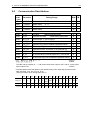
1 OUTLINE
1
1 OUTLINE
1-1
Communication Interface
As an option, the FP23 Series supports two communication interfaces: RS-2323C and
RS-485. Using these communication interfaces, you can set up or read various data
from a personal computer.
The RS-2323C and RS-485 communication interface are data communication standards
determined by the EIA (Electronic Industries Alliance) of the United States. These
standards stipulate electrical and mechanical so-called “hardware” information, and do
not define the software aspects of data transfer procedures. For this reason,
communication is not possible unconditionally even between devices that support the
same interface.
For this reason, the user must be fully familiar with and understand data transfer
specifications and transfer procedures.
The RS-485 interface allows multiple FP23s to be connected in parallel.
Though there are currently few personal computers that support the RS-485 interface,
the RS-485 interface can be used by connecting a third-party RS-232C/RS-485
converter.
1-2
Communication Protocol and Specifications
The FP23 Series supports the SHIMADEN standard protocol and MODBUS
communication protocol.
Common to each protocol
Signal level
EIA RS-232, RS-485 compliant
Communication system
RS-232C 3-line half-duplex system
RS-485 2-line half-duplex multidrop (bus) system
Synchronization system
Start-stop synchronization
Communication distance
RS-232C max. 15m
RS-485 max. 500 m (depending on connection conditions)
Communication speed
2400/4800/9600/19200 bps
Transmission procedure
Non-procedural
Communication delay time
1 to 50 ms
Communication code
ASCII code
Number of connectable
device
RS-232C 1
RS-485
max. 31 (depending on connection conditions)
2
1 OUTLINE
SHIMADEN standard protocol
This is a SHIMADEN proprietary communication protocol.
The table below shows the specifications of this protocol.
Data length
7/8 bits
Parity
EVEN, ODD , NONE
Stop bit
1/2 bits
Communication address
01 to 98
Communication memory mode
EEP/RAM/R_E
Communication BBC
Add/Add two’s cmp/XOR/NONE
MODBUS communication protocol
This is a communication protocol developed for PLCs by Modicon Inc.
Though the specifications of this protocol are open, only the communication protocol is
defined in this protocol, and physical layers such as communication medium are not
stipulated.
The table below shows the specifications of this protocol.
• ASCII mode
Data length
Fixed to 7 bits
Parity
EVEN, ODD , NONE
Stop bit
1 bit, 2 bits
Control code
_CRLF
Error check
LRC
• RTU mode
Data length
Fixed to 8 bits
Parity
EVEN, ODD , NONE
Stop bit
1 bit, 2 bits
Control code
None
Error check
CRC
Function code
03H) Read data
06H) Write data
2 CONNECTING THE CONTROLLER TO A HOST COMPUTER
2
3
CONNECTING THE CONTROLLER
TO A HOST COMPUTER
The FP23 Series controller is connected to the host computer by three lines, send data,
receive data and signal ground.
The following shows connection examples.
For details, refer to the User’s Manual for the host computer.
2-1
When the RS-232C Interface Is Used
Host (9-pin)
PC/AT compatible
machine
SD(3)
RD(2)
SG(5)
RS(7)
CS(8)
DR(6)
ER(4)
FP23
Controller
RD(14)
SD(13)
SG(12)
...Receive data
...Send data
...Signal ground
Numbers in parentheses () are connector pin Nos.
2-2
When the RS-485 Interface Is Used
The I/O logic level of the F23 basically is as follows:
Mark state: - terminal < + terminal Space state: - terminal > + terminal
Note, however, that the + terminal, and – terminal of the controller are high-impedance
before transmission is started, and the above levels are output during transmission.
If necessary, attach a terminator of about 1/2W 120Ω to the endmost terminal (between
+ and – terminals). Operation when a terminator attached to two or more units is not
guaranteed.
4
2 CONNECTING THE CONTROLLER TO A HOST COMPUTER
Host
FG
+
SG
FP23
Controller
1
+(13)
-(14)
SG(12)
Controller
2
+(13)
-(14)
SG(12)
.
.
Controller
N
+(13)
-(14)
SG(12)
Terminator
(120 Ω)
About tri-state output control
When the RS-485 interface is used, the connection becomes a multidrop connection.
For this reason, to avoid conflict between send signals, the transmission output is held at
high-impedance at all times during reception or when communication is not performed.
In tri-state control, a delay of about 1 msec (max.) after end of transmission of the end bit
of the end character up to the return from high impedance is generated.
To absorb this delay time, be sure to set a delay time of several seconds or more when
performing transmission immediately after the host computer ends reception.
END CHARACTER
Send signal
END CHARACTER
1
High-impedance
0
end bit
High-impedance
start bit
end bit
3 COMMUNICATION SETUP PARAMETERS
3
5
COMMUNICATION SETUP PARAMETERS
The FP23 Series has 11 communication setup parameters, of which two are exclusively
for the SHIMADEN standard protocol.
• Setting the communication mode (No.1-1)
• Setting the communication protocol (No.5-8)
• Setting the device address (No.5-8)
• Setting the communication speed (No.5-8)
• Setting the communication memory mode (No.5-8)
• Setting the communication data length (No.5-9)
• Setting the communication parity (No.5-9)
• Setting the communication stop bit (No.5-9)
• Setting the communication delay time (No.5-9)
• Setting the communication control code (No.5-10): SHIMADEN standard protocol only
• Setting the BCC data operation method (No.5-10): SHIMADEN standard protocol only
These parameters can be set or changed only by using the keys on the front panel and
not by communication.
When setting these parameters, refer to the “LCD Flow Chart” in the Instruction Manual
and follow the instructions in this section.
3-1
Setting the Communication Mode (No.1-1)
1-1
AT :
MAN:
COM:
OFF
OFF
COM
CH
1
Setting range
Default
: LOC, COM
: LOC
Set the communication mode.
Note, however, that COM can be only changed to LOC using the front panel keys.
LOC
COM
Note
Only read command enabled by communication (COM LED on front panel
out)
Read and write commands enabled by communication (COM LED on front
panel lit)
When the communication mode is set to COM, changing of all communication
setup parameters is prevented by the key lock.
To prevent uncontrollable situations such as host program runaway,
communication between the FP23 and the host can be forcibly terminated by
holding down the ENT and STEP keys simultaneously for at least three seconds.
6
3 COMMUNICATION SETUP PARAMETERS
3-2
Setting the Communication Protocol (No.5-8)
5-8
COM PROT: SHIMADEN
ADDR:
1
BPS : 9600
MEM : EEP
Setting range : SHIMADEN, MOD_ASC, MOD_RTU
Default
: SHIMADEN
Set the communication protocol.
SHIMADEN
MOD_ASC
MOD_RTU
SHIMADEN standard protocol
MODBUS communication protocol (ASCII mode)
MODBUS communication protocol (RTU mode)
There are two MODBUS communication protocol modes, ASCII mode and RTU mode.
Either of these modes can be selected. Note, however, that all devices on the same
network must be set to the same MODBUS communication protocol mode.
In the ASCII mode, 1-byte (8-bit) data is converted to two ASCII code characters before
it is transferred.
In the RTU mode, 1-byte (8-bit) data is transferred as it is.
For this reason, it can be said that the transfer efficiency of the RTU mode is better than
that of the ASCII mode.
3-3
Setting the Device Address (No.5-8)
5-8
COM PROT: SHIMADEN
ADDR:
1
BPS : 9600
MEM : EEP
Setting range
Default
: 1 to 98
:1
In the case of the RS-232C interface, the connection between the FP23 and the host
computer is a 1:1 connection. However, in the case of the RS-485 interface, the
connection becomes a multidrop connection, which means that a maximum of 31 FP23
units can be connected.
However, actual communication must be performed by a 1:1 connection. For this reason,
unique addresses (machine Nos.) are provided for each of the devices.
Addresses are set within the range 01 to 98, and addresses can be set to a maximum of
31 machines.
The preset address is used as the address for infrared communication with the front
panel of the device.
For details, refer to the Instruction Manual for the Parameter Setup Tool (sold separately).
3 COMMUNICATION SETUP PARAMETERS
3-4
7
Setting the Communication Speed (No.5-8)
5-8
COM PROT: SHIMADEN
ADDR:
1
BPS : 9600
MEM : EEP
Setting range
Default
: 2400/4800/9600/19200 bps
: 9600 bps
Select from 2400, 4800, 9600, 19200 bps as the communication speed, and set.
3-5
Setting the Communication Memory Mode (No.5-8)
5-8
COM PROT: SHIMADEN
ADDR:
1
BPS : 9600
MEM : EEP
Setting range
Default
: EEP/RAM/R_E
: EEP
This device uses non-volatile memory (EEPROM) for storing parameter setups.
As the write cycle or number of times that the EEPROM can be written is already
determined, periodically rewriting SV data, for example, in EEPROM by communication
will shorten the EEPROM’s life.
To prevent this when data is frequently rewritten by communication, the EEPROM can
also be set so that it is not rewritten and only RAM data is overwritten. This will prolong
the life of the EEPROM.
EEP
RAM
R_E
3-6
In this mode, the EEPROM is rewritten each time that data is changed by
communication. For this reason, data is held on the device even if the device
is turned OFF.
In this mode, only RAM data is rewritten and data in EEPROM is not rewritten
even if data is changed by communication. For this reason, data in RAM is
cleared when the device is turned OFF, and the device starts up with the data
in EEPROM when it is turned ON again.
In this mode, SV1 to SV10, OUT, and COM mode data is written only to RAM.
Other data is written to EEPROM.
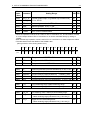
Setting the Communication Data Length (No.5-9)
5-9
COM DATA:
PARI:
STOP:
DELY:
7
EVEN
1
10 ms
7 or 8 bits can be set only in the SHIMADEN standard protocol. The default data length
is 7 bits.
The data length in the MODBUS communication protocol is fixed to 7 bits in the ASCII
mode and 8 bits in the RTU mode.
8
3 COMMUNICATION SETUP PARAMETERS
3-7
Setting the Communication Parity (No.5-9)
5-9
COM DATA:
PARI:
STOP:
DELY:
7
EVEN
1
10 ms
Setting range
Default
: EVEN, ODD, NONE
: EVEN
Set the parity check method for detecting errors in data in data communication.
3-8
Setting the Communication Stop Bit (No.5-9)
5-9
COM DATA:
PARI:
STOP:
DELY:
3-9
7
EVEN
1
10 ms
Setting range
Default
: 1, 2
:1
Setting the Communication Delay Time (No.5-9)
5-9
COM DATA:
PARI:
STOP:
DELY:
7
EVEN
1
10 ms
Setting range
Default
: 1 to 50 ms
: 10 ms
Set the minimum delay time from reception of the communication command up to
transmission.
Note
3-10
• In the case of the RS-485 interface, it sometimes takes time to perform tri-state
control due to the line converter, which may cause signals to collide. This can be
avoided at this time by lengthening the delay time. Particular care must be taken
when communication is set to a low speed (2400 bps).
• The actual delay time from reception of the communication command up to
transmission is the total time required to process commands by the software
added to the above delay time. In particular, it sometimes takes about 400 ms to
process commands in the case of the write command.
Setting the Communication Control Code (No.5-10)
This setting item is available only in the SHIMADEN standard protocol. Set the
communication control code.
5-10
COM
CTRL
STX_EXX_CR
BCC : ADD
Setting range
Default
: STX_ETX_CR, STX_ETX_CRLF,
@_: _CR
: STX_ETX_CR
3 COMMUNICATION SETUP PARAMETERS
3-11
9
Setting the Communication BCC Data Operation Method
(No.5-10)
This setting item is available only in the SHIMADEN standard protocol.
5-10
COM
CTRL : STX_ETX_CR
BCC : ADD
Setting range
Default
: ADD, ADD_two's cmp, XOR, None
: ADD
There are four operation methods for the BCC (Block Check Character) data:
ADD
Addition operation
ADD_two's cmp The two’s complement of the lower 1 byte of the addition operation
result is taken.
XOR
XOR (exclusive OR) operation is performed.
None
BCC operation is not performed.
For details, see “4-2 (3) Details of basic format section II.”
10
3 COMMUNICATION SETUP PARAMETERS
This page left intentionally blank
4 EXPLANATION OF SHIMADEN PROTOCOL
4
11
EXPLANATION OF SHIMADEN PROTOCOL
4-1
(1)
Communication Procedure
Master and slave
The host (personal computer or PLC) is the master.
The FP23 is the slave.
Communication starts by the communication command from the master, and ends by
the communication response from the slave.
Note, however, that a communication response is not performed when an error (e.g.
communication format error or BCC error) occurs, or when a broadcast command is
issued.
(2)
Communication procedure
Communication is performed by a response being returned by the slave to the master.
During communication, the transmission right shifts between the master and the slave.
(3)
Timeout
The FP23 regards instances where reception of the end character does not end within
one second of receiving the start character as a timeout, disables that command, and
stands by for the next command (new start character).
4-2
Communication Format
The FP23 Series supports various protocols, and so various selections can be made by
the communication format (control codes, BCC operation method) or communication
data format (data bit length, parity, stop bit length).
However, for ease of use and to avoid confusion when setting up communications, we
recommend using the following format:
Recommended Format
Control code
STX_ETX_CR
BCC operation method
Data bit length
Parity
Stop bit length
ADD
7
8
EVEN
NONE
1
1
12
(1)
4 EXPLANATION OF SHIMADEN PROTOCOL
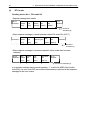
Outline of communication format
The formats of the communications commands sent from the master and the
communication response formats sent from the slave comprise three blocks: basic
format section I, text section and basic format section II.
Basic format sections I and II are common to the Read command (R), Write command
(W) and during communication responses. Note, however, that the operation result data
at that time is inserted as the BCC data of i ((13) and (14)). The text section differs
according to factors such as the command type, data address and communication
response.
Communication command format
Start
character
Text end
character
Command type
Device Subaddress
address
a
b
Number
of data
Start
data address
c
d
e
f
(1)
(2)
(3)
(4)
(5)
(6)
(7)
(8)
STX
STX
0
0
1
2
1
1
R
W
0
0
1
1
0
8
Basic format section I
Data
g
(9) (10)
0
C
End
character
(delimiter)
i
j
h
(11)
0
0
BCC
data
(12) (13) (14) (15) (16)
---,* * * *
ETX
ETX
D
0
A
B
Command type
b
a
Text end
character
Response code
Device Subaddress
address
d
e
g
(1)
(2)
(3)
(4)
(5)
(6)
(7)
(11)
STX
STX
0
0
1
2
1
1
R
W
0
0
0
0
,****
----
Basic format section I
Text section
End character
(delimiter)
BCC
data
Data
c
---
Basic format section II
Text section
Communication response format
Start
character
CR
CR
h
i
j
(12) (13) (14) (15) (16)
ETX
ETX
3
4
E
F
CR
CR
---
Basic format section II
4 EXPLANATION OF SHIMADEN PROTOCOL
(2)
13
Details of basic format section I
a: Start character [(1): 1 digit/STX (02H) or "@" (40H)]
•
•
The start character indicates the start of the communication message.
When the start character is received, it is judged to be the 1st character of a new
communication message.
・ Select the start character and text end character as a pair.
STX (02H) - - - Select by ETX (03H)
"@" (40H) - - - - Select by ": "(3AH)
b: Device address [(2), (3): 2 digits]
•
•
•
•
Specify the device to communicate with.
Specify the address within the range 1 to 98 (decimal).
Binary 8-bit data (1: 0000 0001 to 98: 0110 0010) is divided into upper 4 bits and
lower 4 bits, and converted to ASCII data.
(2): Data obtained by converting the upper 4 bits to ASCII
(3): Data obtained by converting the lower 4 bits to ASCII
Device address=0 (30H, 30H) cannot be used as the device address as it is used
when the broadcast instruction is issued.
c: Subaddress [(4): 1 digit]
•
(3)
In a 1-loop specification, the subaddress is fixed to 1 (31H).
In a 2-loop specification, channel 1 can be accessed by 1 (31H) and channel 2 can
be accessed by 2 (32H).
Details of basic format section II
h: Text end character [(12): 1 digit/ETX (03H) ] or ": " (3AH) ]
•
Indicates the end of the text.
i: BCC data [(13), (14): 2 digits]
•
•
•
The BCC (Block Check Character) data is for checking if there is an error in the
communication data.
When BCC operation results in a BCC error, a no-response state is entered.
There are four types of BCC operation as shown below. These can be set on the
front panel screen.
(1) ADD
Addition operation is performed from start character (1) through to text end
character (12) in ASCII data single characters (1-byte).
(2) ADD_two's cmp
14
4 EXPLANATION OF SHIMADEN PROTOCOL
Addition operation is performed from start character (1) through to text end
character (12) in ASCII data 1-character (1-byte) units, and the two’s
complement of the lower 1 byte of the operation result is taken.
(3) XOR
Exclusive OR is performed from after (device address ((2)) the start character
through to text end character (12) in ASCII data 1-character (1-byte) units.
(4) None
BCC operation is not performed. ((13), (14) is omitted.)
•
•
BCC data is operated in 1-byte (8-bit) units regardless of the data bit length (7 or 8).
The lower 1-byte data of the result of the above operation is divided into upper 4 bits
and lower 4 bits, and converted to ASCII data.
(13): Data obtained by converting the upper 4 bits to ASCII
(14): Data obtained by converting the lower 4 bits to ASCII
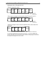
Example 1: iRead command (R) at BCC i Add setting
(1) (2)
STX 0
(3) (4) (5) (6)
1
1
R 0
(7) (8) (9) (10) (12) (13) (14) (15) (16)
1
0
0
9 ETX E
3 CR LF
02H +30H +31H +31H +52H +30H +31H +30H +30H +39H +03H =1E3H
Lower 1 byte of add result (1E3H)
(13): "E" = 45H, (14): "3" = 33H
Example 2: iRead command (R) at BCC i Add_two's cmp setting
(1) (2)
STX 0
(3) (4) (5) (6)
1
1
R 0
(7) (8) (9) (10) (12) (13) (14) (15) (16)
1
0
0
9 ETX 1
D CR LF
02H +30H +31H +31H +52H +30H +31H +30H +30H +39H +03H =1E3H
Lower 1 byte of add result (1E3H)
Two's complement of lower 1 byte (E3H)
(13): "1" = 31H, (14): "D" = 44H
Example 3: iRead command (R) at BCC i XOR setting
(1) (2)
STX 0
(3) (4) (5) (6)
1
1
R 0
(7) (8) (9) (10) (12) (13) (14) (15) (16)
1
0
0
9 ETX 5
9 CR LF
02H 30H A31H A31H A52H A30H A31H 30H 30H 39H 03H =59H
Note that A=XOR
Lower 1 byte of operation result (59H)
(13): "5" = 35H, (14): "9" = 39H
4 EXPLANATION OF SHIMADEN PROTOCOL
15
j: End character (delimiter) [(15), (16): 1 digit or 2 digits/CR or CR LF]
•
•
Indicates the end of the communication message.
The following two types can be selected as the end character:
(15), (16): CR (0DH) (LF is not appended by CR alone.)
(15), (16): CR (0DH) and LF (0AH)
Note
A response is not performed when an error such as follows is recognized in the
basic format section:
• A hardware error occurred.
• The device address and subaddress differ from the address of the specified
device.
• The character specified by the previous communication format is not at the
specified position.
• The BCC operation result differs from the BCC data.
Data conversion converts binary data to ASCII data in 4-bit blocks.
Hex <A> to <F> are expressed in uppercase characters and are converted to
ASCII data.
(4)
Outline of text section
The text section differs according to the command type and communication response.
For details, see “4-3 Details of Read Command (R)” and “4-4 Details of Write Command
(W).”
d: Command type [(5): 1 digit]
•
No response is made when a character other than “R”, “W” and “B” is recognized.
"R" (52H/uppercase character):
Indicates a Read command or a Read command response.
This is used to read (load) various FP23 data from a master personal
computer or PLC.
"W" (57H/uppercase character):
Indicates a Write command or a Write command response.
This is used to write (change) various FP23 data from a master personal
computer or PLC.
"B" (42H/uppercase character):
Indicates a broadcast command.
This is used to batch write (change) data to all devices that support the
broadcast command from a master personal computer or PLC.
16
4 EXPLANATION OF SHIMADEN PROTOCOL
e: Start data address [(6), (7), (8), (9): 4 digits]
•
•
Specifies the read start data address of the Read command (R) or the write start
data of the Write (W) command.
The start data address is specified by binary 16-bit (1 word/0 to 65535) data.
The 16-bit data is divided into 4-bit blocks and then converted to ASCII data.
Binary
(16 bits)
D15,D14,D13,D12
0
0 0 0
D11,D10,D9,D8
0
0 1 1
Hex
0H
"0"
30H
(6)
3H
"3"
33H
(7)
ASCII data
•
D7, D6, D5, D4
0 0 0 0
D3, D2, D1, D0
1 0 1 0
0H
"0"
30H
(8)
AH
"A"
41H
(9)
For details on data addresses, see “6-2 Communication Data Addresses.”
f: Number of data [(10): 1 digit]
•
•
•
Specifies the number of read data in the Read command (R) and the number of
write data in the Write command (W).
The number of data is specified by converting binary 4-bit data to ASCII data.
With the Read command (R), the number of data can be specified within the range
1: "0" (30H) to 10: "9" (39H).
With the Write command (W), the number of data is fixed at 1: "0" (30H).
The actual number of data is “number of data=specified data numerical value + 1”.
g: Data [(11): Number of digits determined by number of data]
g(11)
Lower 4th digit
3rd digit
2nd digit
Upper 1st digit
nth data
Lower 4th digit
3rd digit
2nd digit
Upper 1st digit
2nd data
Lower 4th digit
","
2CH
3rd digit
1st data
2nd digit
•
Specifies the number of write data (change data) of the Write command (W) or read
data during a Read command (R) response.
The following shows the data format:
Upper 1st digit
•
4 EXPLANATION OF SHIMADEN PROTOCOL
•
•
•
•
•
17
The data is always prefixed by a comma (“, “2CH) to indicate that what follows the
comma is the data.
The number of data follows the number of data (f: (10)) in the communication
command format.
One item of data is expressed in binary 16-bit (1 word) units without a decimal point.
The position of the decimal point is determined by each data.
16-bit data is divided into 4-bit blocks, and each block is converted to ASCII data.
For details of data, see “4-3 Details of Read Command (R)” and “4-4 Details of
Write Command (W).”
e: Response code [(6), (7): 2 digits]
•
Specifies the response code for the Read command (R) and Write command.
Binary 8-bit data (0 to 255) is divided into upper 4 bits and lower 4 bits, and each is
converted to ASCII data.
(6): Data obtained by converting upper 4 bits to ASCII
(7): Data obtained by converting lower 4 bits to ASCII
•
In the case of a normal response, "0" (30H) and "0" (30H) are specified.
In the case of an error response, the error code No. is specified after conversion to
ASCII data.
For details on response codes, see “4-6 Details of Response Codes.”
4-3
Details of Read Command (R)
The Read command (R) is used to read (load) various FP23 data from a master
personal computer or PLC.
(1)
Format of Read command (R)
•
The following shows the format of the text section of the Read command (R).
Basic format section I and basic format section II are common to all commands and
command responses.
Text section
d
(5)
e
(6)
(7)
f
(8)
(9)
(10)
R
0
4
0
0
9
52H 30H 34H 30H 30H 39H
•
•
•
D ((5)) indicates the Read command.
It is fixed to “R” (52H).
E ((6) to (9)) specifies the start data address of the data to read.
F ((10)) specifies the number of data (words) to read.
18
4 EXPLANATION OF SHIMADEN PROTOCOL
•
The above command is as follows:
Read start data address =0400H
=0000 0100 0000 0000
Number of read data
=9H
=1001
=9
(actual number of data) =10 (9+1)
(Hex)
(binary)
(Hex)
(binary)
(decimal)
In other words, in this example, reading of 10 continuous items of data from data
address 0400H is specified.
(2)
Format of normal response to Read command (R)
•
The following shows the format (text section) of a normal response to the Read
command (R).
Basic format section I and basic format section II are common to all commands and
command responses.
Text section
d
(5)
e
(6)
g
(11)
(7)
1st data
R
0
0
,
52H 30H 30H 2CH
•
•
•
2nd data
0
0
1
E
0
0
7
8
30H 30H 31H 45H 30H 30H 37H 38H
10th data
0
0
7
8
30H 30H 37H 38H
<R(52H)> indicating a response to the Read command (R) is inserted at d ((5)).
<00(30H and 30H)> indicating a normal response to the Read command (R) is
inserted at e ((6) and (7)).
The response data to the Read command (R) is inserted at g ((11)).
<","(2CH)> indicating the data of the data description is inserted at the beginning of
the text section.
Data in inserted following the beginning of the text section in order from <data of the
read start data address> for the number of <read data number>.
Nothing is inserted between data items.
One item of data is expressed in binary 16-bit (1 word) units without a decimal point,
and is converted to ASCII data in 4-bit blocks before it is inserted.
The position of the decimal point is determined by each data.
The number of characters of the response data is “number of characters=1+4 x
number of read data”.
4 EXPLANATION OF SHIMADEN PROTOCOL
•
In actual terms, the following data is returned in order as the response data to the
Read command (R).
Data address
16 bits (1 word)
Read start
data address
(0400H)
Number of read data
(9H: 10 data)
(3)
19
Data
16 bits (1 word)
Hex
Hex
0
0400
001E
30
1
0401
0078
120
2
0402
001E
30
3
0403
0000
0
4
0404
0000
0
5
0405
0000
0
6
0406
03E8
1000
7
0407
0028
40
8
0408
001E
30
9
0409
0078
120
040A
001E
30
040B
0000
0
040C
0000
0
Decimal
Format of error response to Read command (R)
•
The following shows the format (text section) of an error response to the Read
command (R).
Basic format section I and basic format section II are common to all commands and
command responses.
Text section
d
(5)
e
(6)
(7)
R
0
7
52H 30H 37H
•
•
<R(52H)> indicating a response to the Read command (R) is inserted at d ((5)).
A response code indicating an error response to the Read command (R) is inserted
at e ((6) and (7)).
Response data is not inserted in the case of an error response.
For details on error codes, see “4-6 Details of Response Codes.”
20
4 EXPLANATION OF SHIMADEN PROTOCOL
4-4
Details of Write Command (W)
The Write command (W) is used to write (change) various data on FP23 from a master
personal computer or a PLC.
Caution
To use the Write command, the communication mode must be changed from
LOC to COM.
The communication mode cannot be changed using the keys on the front panel.
To change the communication mode, send the following command from the
master.
Command format
When ADDR=1, CTRL=STX_ETX_CR, BCC=ADD
STX
0
1
1
W
0
1
8
C
0
,
0
0
0
1 ETX E
7
CR
02H 30H 31H 31H 57H 30H 31H 38H 43H 30H 2CH 30H 30H 30H 31H 03H 45H 37H 0DH
If a normal response is returned to the above command, the COM LED on the
front panel lights and the communication mode switches to COM.
(1)
Format of Write command (W)
•
The following shows the format of the text section in the case of the Write command
(W).
Basic format section I and basic format section II are common to all commands and
command responses.
Text section
d
(5)
g
(11)
Write data
W
0
4
0
1
0
,
0
0
7
D
57H 30H 34H 30H 31H 30H 2CH 30H 30H 37H 44H
•
•
•
e
(6)
(7)
(8)
(9)
f
(10)
D ((5)) indicates the Write command.
It is fixed to “W” (57H).
E ((6) to ((9)) specifies the start data address of the write (change) data.
F ((10)) specifies the number of write (change) data.
The number of write data is fixed to 1: "0" ( 30H )
4 EXPLANATION OF SHIMADEN PROTOCOL
•
21
g ((11)) specifies the write (change) data.
<","(2CH)> indicating the data of the data description is inserted at the
beginning of the write.
Next, the write data is inserted.
One item of data is expressed in binary 16-bit (1 word) data without a decimal
point, and is converted to ASCII data in 4-bit blocks before it is inserted.
The position of the decimal point is determined by each data.
•
The above command is as follows:
Write leading start address =0401H
=0000 0100 0000 0001
Number of write data
=0H
=0000
=0
(actual number of data) =1 (0+1)
Write data
=007DH
=0000 0000 0111 1110
=125
(Hex)
(binary)
(Hex)
(binary)
(decimal)
(Hex)
(binary)
(decimal)
In other words, in this example, writing (change) of one item of data (125 decimal) to
data address 0401H is specified.
Data address
16 bits (1 word)
Write start data address
(300H)
Number of writer data
1 (0H)
0
Data
16 bits (1 word)
Hex
Decimal
Hex
Decimal
0400
1024
00C8
200
0401
1025
007D
125
0402
1026
0078
120
22
4 EXPLANATION OF SHIMADEN PROTOCOL
(2)
Format of normal response to Write command (W)
•
The following shows the format (text section) of a normal response to the Write
command (W).
Basic format section I and basic format section II are common to all commands and
command responses.
Text section
d
(5)
e
(6)
(7)
W
0
0
57H 30H 30H
•
•
(3)
<W(57H)> indicating a response to the Write command (W) is inserted at d ((5)).
Response codes <00(30H and 30H)> indicating a normal response to the Write
command (W) are inserted at e ((6) and (7)).
Format of error response to Write command (W)
•
The following shows the format (text section) of an error response to the Write
command (W).
Basic format section I and basic format section II are common to all commands and
command responses.
Text section
d
(5)
e
(6)
(7)
W
0
9
57H 30H 39H
•
•
<W(57H)> indicating a response to the Write command (W) is inserted at d ((5)).
A response code indicating an error response to the Read command (R) is inserted
at e ((6) and (7)).
For details on error codes, see “4-6 Details of Response Codes.”
4 EXPLANATION OF SHIMADEN PROTOCOL
4-5
23
Details of Broadcast Command (B)
The Broadcast command (B) is used to batch write (change) data to all devices that
support the broadcast command from a master personal computer or PLC.
The broadcast command does not have a communication response.
(1)
Format of broadcast command
For details of parameters that can be broadcasted, see B on the right side of “Chapter 6
List of Communication Data Addresses.”
Ex: AT (auto tuning) execution
Device address: 00, sub-address: 1 or 2
STX
0
0
1
B
0
1
8
4
,
0
0
0
1 ETX 9
2
CR
02H 30H 30H 31H 42H 30H 31H 38H 34H 2CH 30H 30H 30H 31H 03H 39H 32H 0DH
24
4 EXPLANATION OF SHIMADEN PROTOCOL
4-6
(1)
Details of Response Codes
Type of response codes
Communication responses to the Read command (R) and Write command (W) must
contain a response code.
There are two types of response codes: normal response code and error response code.
Response codes are expressed as binary 8-bit data (0 to 255). The table below shows
the details of response codes.
Response Code List
Response Code
Code Type
(2)
Description
Binary
ASCII
0000 0000
"0","0":30H,30H
Normal response
0000 0001
"0","1":30H,31H
A hardware error such as framing overrun
Hardware error in text
or parity has been detected in the data of
section
the text section.
0000 0111
"0","7":30H,37H
Format error in text
section
The format of the text section differs
from the predetermined format.
0000 1000
"0","8":30H,38H
Data format data
address, number of
data error in text
section
The format of the text section differs
from the predetermined format, or the
data address and number of data are other
than specified.
0000 1001
"0","9":30H,39H
Data error
The write data exceeds the settable range
of that data.
0000 1010
"0","A":30H,41H
Execution command
error
An execution command (e.g. MAN) was
received when it could not be accepted.
Normal response code for Read command
(R) or Write command (W)
0000 1011
"0","B":30H,42H
Write mode error
When data that must not be rewritten
depending on the data type, a write
command containing that data was
received.
0000 1100
"0","C":30H,43H
Specification, option
error
A write command containing data of an
unmounted specification or option was
received.
Order of priority of response codes
The smaller the value of the response code becomes, the higher the priority of the
response code.
When multiple response codes have been issued, the response code having the higher
or highest priority is returned.
5 EXPLANATION OF MODBUS COMMUNICATION PROTOCOL
5
25
EXPLANATION OF MODBUS COMMUNICATION
PROTOCOL
The MODBUS communication protocol has two transfer modes: ASCII mode and RTU
mode.
5-1
(1)
Outline of Transfer Mode
ASCII mode
The 8-bit binary data in commands is divided into upper 4 bits (Hex) and lower 4 bits
(Hex), each of which is sent as ASCII characters.
Data configuration
Start bit
Data bit
Parity bit
Stop bit
Error check
Data communication interval
(2)
1 bit
7 bits/fixed
EVEN, ODD, NONE selectable
1 bit, 2 bits selectable
LRC (Longitudinal Redundancy Check)
1 sec or less
RTU mode
The 8-bit binary data in commands is sent as it is.
Data configuration
Start bit
Data bit
Parity bit
Stop bit
Error check
Data communication interval
5-2
(1)
1 bit
8 bits/fixed
EVEN, ODD, NONE selectable
1 bit, 2 bits selectable
CRC-16 (Cyclic Redundancy Check)
3.5 character transmission time or less
Configuration of Messages
ASCII mode
In this mode, messages are configured to begin with a start character [: (colon) (3AH) ],
and end with an end character [CR (carriage return) (ODH) ] followed by a LF (line
feed) (0AH) ].
Header
(:)
Slave
address
Function code Data
Error check LRC
Delimiter
(CR)
Delimiter
(LF)
26
5 EXPLANATION OF MODBUS COMMUNICATION PROTOCOL
(2)
RTU mode
In this mode, messages begin after an idle time of 3.5 characters transfer time or more,
and end after an idle time of 3.5 characters transfer time or more has elapsed.
Idle 3.5
Slave
characters address
5-3
Function
code
Data
Error check CRC
Idle 3.5
characters
Slave Address
The slave address is the device No. of the slave, and is set within the range 0 to 99.
The master recognizes each of the slaves by specifying the slave address in request
messages.
The slave notifies the master of which slave is responding by setting and returning its
own slave address to the response message.
Slave address 0 is the broadcast address and can specify all slaves.
In the case of a broadcast, slaves do not return a response.
In the 1-loop specification, the slave address is the same as the device address.
In the 2-loop specification, the slave address of channel 1 is the same as the device
address, and the slave address of channel 2 is the device address+1.
5-4
Function Codes
A function code is a code for instructing the type of operation to the slave.
Function Code
Details
03 (03H)
Reads setting values and information from slaves.
06 (06H)
Writes to slave.
These function codes are also used for indicating whether the response message
returned to the master by the slave is a normal response (positive response) or that
some error has occurred (negative response).
In a positive response, the original function code is set and returned.
In a negative response, the MSB of the original function code is set to “1” and returned.
For example, when “10H” has been mistakenly set as the function code, and the request
message has been sent to the slave, “1” is set to the MSB and returned as “90H” as this
function code is non-existent.
Also, in the case of a negative response, an error code is set to the response message
and returned to notify the master of which type of error has occurred.
5 EXPLANATION OF MODBUS COMMUNICATION PROTOCOL
5-5
Error Code
Details
1 (01H)
illegal Function (non-existent function)
2 (02H)
illegal data address (non-existent data address)
3 (03H)
illegal data value (value out of setting range)
27
Data
The structure of data differs according to the function code.
With request messages from the master, data is configured by data item, number of data
and setting data.
With response messages from a slave, data is configured by number of bytes or data in
response to the request, and in the case of a negative response, an error code.
The valid data range is -32768 to 32767 (8000H to 7FFFH).
5-6
Error Check
The error check method differs according to the transfer mode.
(1)
ASCII mode
As the error check for the ASCII mode, calculate the LRC up to the end of the data from
the slave address, convert the resulting 8-bit data to two ASCII characters and append it
to the data.
LRC calculation method
1.
2.
3.
4.
5.
6.
(2)
Create a message in the RTU mode.
Add up to the end of the data from the slave address, and substitute with x.
Take the 2’s complement (invert bits) of x, and substitute with x.
Add “1” to x, and substitute with x.
Append to the data taking x to be the LRC.
Convert the message to ASCII characters.
RTU mode
As the error check for the RTU mode, calculate the CRC-16 up to the end of the data
from the slave address, and append the resulting 16-bit data to the data in order lower
bits then upper bits.
28
5 EXPLANATION OF MODBUS COMMUNICATION PROTOCOL
CRC-16 calculation method
By the CRC method, the information to be sent is divided by a generating function, and
the information is appended with the remainder and then sent.
Generating function: X16+X15+X2+1
Initialize the data of CRC (taken to be x) to (FFFFH).
Exclusive-OR the 1st data with x, and substitute with x.
Shift x to the right by one bit, and substitute with x.
If the shift results in a carry, exclusive-OR the result of (3) with a fixed value
(A001H), and substitute with x. If the shift does not result in a carry, go to step 5.
Repeat steps 3 and 4 until x is shifted eight times.
Exclusive-OR the next data with x, and substitute with x.
Repeat steps 3 to 5.
Repeat steps 3 to 5 until the last data.
Append the data to the message in order lower bits then upper bits taking x to
be CRC-16.
1.
2.
3.
4.
5.
6.
7.
8.
9.
5-7
Examples of Messages
(1)
ASCII mode
Reading device No.1 FIX mode SV
• Request message from master
Header
Slave
address
Function Data
code
address
Number of
data
Error check
Delimiter
LRC
(: )
(01H)
(03H)
(0300H)
(0001H)
(F8H)
(CR• LF)
1
2
2
4
4
2
2
Number of
characters (17)
• Slave response message in normal operation (when FIX mode SV=10.0°C)
Header
Slave
address
Function Function
code
code
Data
Error check
Delimiter
LRC
(: )
(01H)
(03H)
(02H)
(0064H)
(96H)
(CR• LF)
1
2
2
2
4
2
2
Number of
characters (15)
5 EXPLANATION OF MODBUS COMMUNICATION PROTOCOL
29
• Slave response message in erroneous operation (when a data item has been
mistaken)
Heade Slave
r゙
address
unction
code
Error code
Error check
Delimiter
LRC
(: )
(01H)
(83H)
(02H)
(7AH)
(CR• LF)
1
2
2
2
2
2
Number of characters (11)
In a response message during normal operation, “1” is set to the MSB of the function
code (83H). An error code 02H (non-existent data address) is returned as the response
message for the error content.
Writing device No.1, FIX mode SV=10.0°C
• Request message from master
Header
Slave
address
Function
code
Data
address
Data
Error check
Delimiter
LRC
(: )
(01H)
(06H)
(0300H)
(0064H)
(92H)
(CR• LF)
2
2
4
4
2
2
1
Number of
characters (17)
• Slave response message in normal operation (when FIX mode SV=10.0°C)
Header
Slave
address
Function
code
Data
address
Data
Error check
Delimiter
LRC
(: )
(01H)
(06H)
(0300H)
(0064H)
(92H)
(CR•
LF)
1
2
2
4
4
2
2
Number of
characters (17)
• Response message on slave in erroneous operation (when a value outside of the
range is set)
Header
Slave
address
Function
Error code
code
Error check
Delimiter
LRC
(: )
(01H)
(86H)
(03H)
(76H)
(CR• LF)
1
2
2
2
4
2
Number of characters (13)
In a response message during occurrence of an error, “1” is set to the MSB of the
function code (86H). An error code 03H (value outside of setting range) is returned as
the response message for the error content.
30
(2)
5 EXPLANATION OF MODBUS COMMUNICATION PROTOCOL
RTU mode
Reading device No.1, FIX mode SV
• Request message from master
Idle 3.5
Slave
characters address
Function Data
code
address
Number of Error check
data
CRC
(01H)
(03H)
(0300H)
(0001H)
(844EH)
1
1
2
2
2
Idle 3.5
characters
Number of
characters (8)
• Slave response message in normal operation (when FIX mode SV=10.0°C)
Idle 3.5
Slave
characters address
Function Number of
Data
code
response bytes
Error check Idle 3.5
CRC
characters
(01H)
(03H)
(02H)
(0064H) (B9AFH)
1
1
1
2
2
Number of
characters (7)
• Slave response message in erroneous operation (when a data item has been
mistaken)
Idle 3.5
Slave
Function
characters address code
Error
code ゙
Error check
LRC
(01H)
(83H)
(02H)
(C0F1H)
1
1
1
2
Idle 3.5
characters
Number of characters (5)
In a response message during normal operation, “1” is set to the MSB of the function
code (83H). An error code 02H (non-existent data address) is returned as the response
message for the error content.
5 EXPLANATION OF MODBUS COMMUNICATION PROTOCOL
31
Setting device No.1, FIX mode SV=10.0°C
• Request message from master
Idle 3.5
Slave Function
characters address code
Data
address
Data
Error
check
CRC
(01H)
(06H)
(0300H)
(0064H)
(8865H)
1
1
2
2
2
Idle 3.5
characters
Number of
characters (8)
• Slave response message in normal operation (when FIX mode SV=10.0°C)
Idle 3.5
Slave Function
characters address code
Data
address
Data
Error check Idle 3.5
CRC
characters
(01H)
(06H)
(0300H)
(0064H)
(8865H)
1
1
2
2
2
Number of
characters (8)
• Response message on slave in erroneous operation (when a value outside of the
range is set)
Idle 3.5
Slave
Function
characters address code
Error
code ゙
Error
check
CRC
(01H)
(86H)
(03H)
(0261H)
1
1
1
2
Idle 3.5
characters
Number of characters (5)
In a response message during occurrence of an error, “1” is set to the MSB of the
function code (86H). An error code 03H (value outside of setting range) is returned as
the response message for the error content.
32
5 EXPLANATION OF MODBUS COMMUNICATION PROTOCOL
This page left intentionally blank
6 LIST OF COMMUNICATION DATA ADDRESSES
6
LIST OF COMMUNICATION DATA ADDRESSES
6-1
(1)
33
Outline of Communication Data Address
Data address and reading/writing the data address
The data address expresses binary in (16-bit data) 4-bit blocks.
• R/W:
• R:
• W:
Data that can be read and written
Read-only data
Write-only data
When a read-only data address is specified in the Write command (W), a data address
error occurs, and the “data format, data address and data number error of the text
section” of error response codes “0 (30H)” and “8 (38H)” are returned.
(2)
Reading/writing parameters in a 2-loop specification
In a 2-loop specification, the value of the parameter corresponding to each loop can be
read by sub-address=1/2 in the case of the SHIMADEN standard protocol, and by slave
address=device address/device address+1 in the case4 of the MODBUS
communication protocol.
Details of parameters having values for each of these loops are indicated by “T” (support
of sub-address) at the right edge of the communication addresses shown below.
(3)
Reading/writing “reserved” in the parameter section
When an address not in the list or address indicated as “<reserved>” are read by the
Read command (R), "0000H" is returned.
When a part indicated as “<reserved>” is written by the write (W) command, the normal
response codes "0 (30H)" and "0 (30H)" are returned. Data, however, is not rewritten.
(4)
Reading/writing option-related parameters
When the data address of parameters for unmounted options are specified, the
“specification, option error” of error response codes "0 (30H)" and "C (43H)" are returned
for both the Read command (R) and Write command (W).
(5)
Parameters not displayed on the front panel
Even parameters that are not indicated (used) on the front panel display can be
read/written by communication depending on the operation and setup specifications.
34
6 LIST OF COMMUNICATION DATA ADDRESSES
(6)
Handling data
As each data is binary (16-bit data) without a decimal point, the data type and presence
of a decimal point must be checked.
For details of this, refer to the Instruction Manual for this device.
Ex: How to express data with a decimal point
20.0%
100.00°C
-40.00°C
200 →
10000 →
-4000 →
Hex data
00C8
2710
F060
For the data of unit UNIT, the decimal point position is determined by the measuring
range.
Otherwise, data is handled as signed binary (16-bit data: -32768 to 32767).
Logic/logic operation cause parameters
With the logic/logic operation cause, binary 16-bit data is expressed by two data items for
a single address, divided into the upper 8 bits and the lower 8 bits.
Ex:
EV1 logic 1:
Logic operation cause 1:
01H (INV)
08H (TS8)
Address
Upper 8 bits
Upper 8 bits
Data
0380
01H
TS8
08H
Likewise, the channel information/operation mode of EV1 to 3 and DO1 to 13 are
expressed as two data items for a single address.
(7)
Execution of broadcast
In the SHIMADEN standard protocol, use the “B” command.
In the MODBUS communication protocol, set “0” to the slave address.
Parameters that can be broadcast are indicated by “B” (broadcast) at the right edge of
the communication addresses show below.
(8)
Annotation of time data
For details of how time data (hours/mins/secs) is annotated, refer to the following
example:
Ex:
1 sec 00: 01 → 0x0001
1 hour 01: 00 → 0x0100
60 secs (0x0060) will result in a write error.
59 secs 00: 59 → 0x0059
99 hours 59 mins 99:59 → 0x9959
6 LIST OF COMMUNICATION DATA ADDRESSES
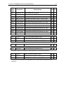
6-2
35
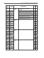
Communication Data Address
Data
Addr.
(Hex)
Parameter
Setting Range
R/W T/B
0040
S_CODE1
Series code 1
“F”, “P”
R
-
0041
S_CODE2
Series code 2
“2”, “3”
R
-
0042
S_CODE3
Series code 3
R
-
0043
S_CODE4
Series code 4
R
-
0100
PV_W
PV value
R
T
0101
SV_W
Execution SV value
R
T
0102
OUT1_W
Control output 1 : -5.0 to 105.0%
R
-
0103
OUT2_W
Control output 2 : -5.0 to 105.0%
R
-
0104
EXE_FLG
Operation flag (See the detailed explanation below.)
R
T
0105
EV_FLG
Event output flag (See the detailed explanation below.)
R
-
0107
EXE_PID
Execution PID No.: 0 (PID No..1) to 9 (PID No.10)
R
T
0109
HB_W
HB current value (current at output ON) 0.0 to 55.0A
R
-
010A
HL_W
HL current value (current at output OFF) 0.0 to 55.0A
R
-
010B
DI_FLG
DI input state flag (See the detailed explanation below.)
R
-
: Within measuring range
: Within setting value limiter
• , ,
,
=7FFFH
=8000H
The HBL and HLA display is -----. HB current value when output is OFF, and HL current value
when output is ON
=7FFEH
• The table below shows the details of the operation flag, Even output flag and the DI input
state flag (EXE_FLG, EV_FLG, DI_FLG).
(during no action: bit=0, during action: bit=1)
EXE_FLG
EV_FLG
DI_FLG
D15
D14
D13
D12
D11
D10
0
0
0
0
Z/S
0
DO13 DO12 DO11 DO10 DO9 DO8
0
0
0
0
0
0
D9
AT
WAIT
D8
D7
D6
D5
D4
D3
D2
D1
D0
COM
0
0
0
0
0
0
MAN
AT
DO7
DO6 DO5 DO4 DO3 DO2 DO1 EV3 EV2 EV1
DI10
DI9
DI8
DI7
DI6
DI5
DI4
DI3
DI2
DI1
36
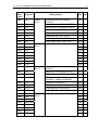
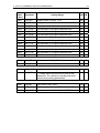
6 LIST OF COMMUNICATION DATA ADDRESSES
Data
Addr.
(Hex)
Parameter
0110
UNIT
0111
RANGE
0112
0113
0114
0115
Setting Range
R/W T/B
Measurement unit 0:°C 1:°F 2: % 3: K 4:
NONE
R
T
Measuring range 0 to 19: Thermocouple 31 to 58:
Resistor
71 to 77: Voltage mV 81 to 87: Voltage V
(See “7-1 Setting Range Code Table.”.)
R
T
CJ
Cold junction compensation 0: Internal 1: External
R
T
DP
PV decimal point position 0: XXXXX 1: XXXX.X
2: XXX.XX 3: XX.XXX 4: X.XXXX
R
T
PV scaling lower/upper limit
At linear input: -19999 to 30000Unit
At resistor, thermocouple input: Measuring range is
displayed.
R
T
R
T
T
SC_L
SC_H
0116
DPFLG
Number of digits past decimal point 0: Normal 1: Short
R
0120
E_PRG
Program action flag (See the detailed explanation below.)
R
T
• The table below shows the details of the program operation flag.
(during no action: bit=0, during action: bit=1)
PRG EXE
_FLG
0121
0122
0123
0124
0125
0126
0129
D15
D14
D13
D12
D11
D10
PRG
0
0
0
0
UP
E_PTN
E_LNK
E_RPT
E_STP
E_TIM
E_PID
E_STPRPT
D9
LVL
D8
DW
D7
RUN
WAIT
D6
0
D5
SO
HLD
D4
0
D3
D2
D1
D0
ADV GUA HLD RUN
Program execution pattern No. : 1 to 20
Program execution link count
: 0 to 9999
Program execution pattern count : 1 to 9999
Program execution step No.
: 0 to 400
Program execution remaining step time : 00: 01 to 99:59
Program execution PID No.
: 0 to 10
Program execution step count : 1 to 9999
R
R
R
R
R
R
R
T
T
T
T
T
T
T
• The above seven parameters return 7FFE excluding when E_PRG is in the program mode
and in a RUN state.
0141
DES
Servo target opening value (enabled when feedback is
ON)
0142
POSI
Servo opening value (enabled when feedback is ON) :
0 to 100
R
-
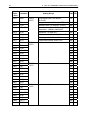
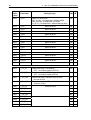
6 LIST OF COMMUNICATION DATA ADDRESSES
37
Data
Addr.
(Hex)
Parameter
Setting Range
0182
OUT1_W
W
-
0183
OUT2_W
Control system output 1/2 (possible only in MAN mode) :
0.0 to 100.0%
W
-
0184
AT
Auto tuning execution 0: OFF 1: ON
W
T/B
0185
MAN
Manual operation 0: OFF 1: ON
W
T/B
018C
COM
Communication mode 0: LOC 1: COM
W
B
018D
COMDI
EV1-3, DO1-13 direct control
W
B
R/W T/B
• When the operation mode is set to LOGIC for EV1 to 3 and DO1 to 3, and to DIRECT for DO6
to 15, the output values of EV1 to 3 and DO1 to 15 can be controlled directly by writing to
COMDI.
When another logic operation cause is set for EV1 to 3 and DO1 to 3, these outputs are ORed.
• The table below shows the details of the COMD1 data.
(during no action: bit=0, during action: bit=1)
D15
COMDI
_FLG
D14
D13
D12
DO13 DO12 DO11 DO10
D11
D10
D9
D8
D7
D6
D5
D4
D3
DO9 DO8 DO7 DO6 DO5 DO4 DO3 DO2 DO1
D2
D1
D0
EV3
EV2
EV1
0190
RUN/RST
Program reset 0: RESET 1: RUN
W
T/B
0191
HLD
Program hold 0: OFF 1: ON
W
T/B
0192
ADV
Program Advance 0: OFF 1: ON
W
T/B
0244
AT
Auto tuning execution (CH1/CH2 simultaneous) 0: OFF 1: ON
W
B
0245
MAN
Manual operation (CH1/CH2 simultaneous)
W
B
0250
RUN/RST
Program reset (CH1/CH2 simultaneous)
W
B
0251
HLD
Program hold (CH1/CH2 simultaneous)
0: OFF 1: ON
W
B
0252
ADV
Program Advance (CH1/CH2 simultaneous) 0: OFF 1: ON
W
B
0280
PV1
CH1 measuring range: Within measuring range
R
-
0281
PV2
CH2 measuring range: Within measuring range
R
-
0300
FIX_SV
FIX mode SV value : Within SV limiter setting range
R/W
T
030A
SV_L
Lower limit SV value setting limiter
R/W
T
R/W
T
0: OFF 1: ON
0: RESET 1: RUN
: Within measuring range (note that SV Limit_L<SV Limit_H)
030B
SV_H
Upper limit SV value setting limiter
: Within measuring range (note that SV Limit_L<SV Limit_H)
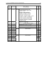
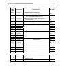
38
6 LIST OF COMMUNICATION DATA ADDRESSES
Data
Addr.
(Hex)
Parameter
Setting Range
R/W T/B
0380
EV1_LSRC/LOG1 EV1 logic 1/logic operation cause1
Logic 1 (upper 8 bits)
0: BUF 1: INV 2: FF
Logic operation cause1 (lower 8 bits)
0: None 1: TS1 2: TS2 3: TS3 4: TS4
5: TS5 6: TS6 7: TS7 8: TS8 9: TS1-C2
10: TS2-C2 11: TS3-C2 12: TS4-C2
13: TS5-C2 14: TS6-C2 15: TS7-C2
16: TS8-C2 17: DI1
18: DI2
19: DI3 20: DI4 21: DI5 22: DI6
23: DI7 24: DI8 25: DI9 26: DI10
0381
EV1_LSRC/LOG2 EV1 logic 2/logic operation cause2 (same as above) R/W -
0382
EV1_LMD
0384
EV2_LSRC/LOG1 EV2 logic 1/logic operation cause1 (same as above) R/W -
0385
EV2_LSRC/LOG2 EV2 logic 2/logic operation cause2 (same as above) R/W -
0386
EV2_LMD
0388
EV3_LSRC/LOG1 EV3logic 1/logic operation cause1 (same as above) R/W -
0389
EV3_LSRC/LOG2 EV3logic 2/logic operation cause2 (same as above) R/W -
038A
EV3_LMD
EV3 logic operation mode 0: AND 1: OR 2: XOR
038C
DO1_LSRC/LOG1
DO1logic 1/logic operation cause1 (same as above) R/W -
038D
DO1_LSRC/LOG2
DO1logic 2/logic operation cause2 (same as above) R/W -
038E
DO1_LMD
DO1 logic operation mode 0: AND 1: OR 2: XOR
0390
DO2_LSRC/LOG1
DO2logic 1/logic operation cause1 (same as above) R/W -
0391
DO2_LSRC/LOG2
DO2logic 2/logic operation cause2 (same as above) R/W -
0392
DO2_LMD
DO2 logic operation mode 0: AND 1: OR 2: XOR
0394
DO3_LSRC/LOG1
DO3logic 1/logic operation cause1 (same as above) R/W -
0395
DO3_LSRC/LOG2
DO3logic 2/logic operation cause2 (same as above) R/W -
0396
DO3_LMD
DO3 logic operation mode 0: AND 1: OR 2: XOR
R/W -
0398
DO4_SRC1
DO4 logic operation cause
R/W -
039A
DO4_LMD
DO4 logic operation mode 0: Timer 1: Counter
R/W -
039B
DO4_LTM
DO4 logic operation counter OFF, 1 to 5000s
R/W -
039C
DO5_SRC1
DO5 logic operation cause
R/W -
039E
DO5_LMD
DO5 logic operation mode 0: Timer 1: Counter
R/W -
039F
DO5_LTM
DO5 logic operation counter OFF, 1 to 5000s
R/W -
EV1 logic operation mode 0: AND 1: OR 2: XOR
EV2 logic operation mode 0: AND 1: OR 2: XOR
R/W -
R/W -
R/W -
R/W -
R/W -
R/W -
6 LIST OF COMMUNICATION DATA ADDRESSES
Data
Addr. Parameter
(Hex)
0400
PB1
0401
39
Setting Range
PID01OUT1
R/W T/B
Proportional band: 0.0 to 999.9%
(0.0=OFF)
R/W
-
IT1
Integral time: 0 to 6000Sec (0=OFF)
R/W
-
0402
DT1
Derivative time: 0 to 3600Sec (0=OFF)
R/W
-
0403
MR1
Manual reset: -50.0 to 50.0%
R/W
-
0404
DF1
Hysteresis: 1 to 9999 Unit
R/W
-
0405
O11_L
Output lower limit: 0.0 to 100.0%
R/W
-
0406
O11_H
Output upper limit: 0.0 to 100.0%
R/W
-
0407
SF1
Target value function: 0.00 to 1.00
R/W
-
0408
PB2
R/W
-
0409
IT2
R/W
-
040A
DT2
R/W
-
040B
MR2
R/W
-
040C
DF2
R/W
-
040D
O12_L
R/W
-
040E
O12_H
R/W
-
040F
SF2
R/W
-
0410
PB3
R/W
-
0411
IT3
R/W
-
0412
DT3
R/W
-
0413
MR3
R/W
-
0414
DF3
R/W
-
0415
O13_L
R/W
-
0416
O13_H
R/W
-
0417
SF3
R/W
-
0418
PB4
R/W
-
0419
IT4
R/W
-
041A
DT4
R/W
-
041B
MR4
R/W
-
041C
DF4
R/W
-
041D
O14_L
R/W
-
041E
O14_H
R/W
-
041F
SF4
R/W
-
PID02OUT1
PID03OUT1
PID04OUT1
Same as above
Same as above
Same as above
40
6 LIST OF COMMUNICATION DATA ADDRESSES
Data
Addr.
(Hex)
Parameter
0420
PB5
0421
Setting Range
PID05OUT1
R/W T/B
Proportional band: 0.0 to 999.9%
(0.0=OFF)
R/W
-
IT5
Integral time: 0 to 6000Sec (0=OFF)
R/W
-
0422
DT5
Derivative time: 0 to 3600Sec (0=OFF)
R/W
-
0423
MR5
Manual reset: -50.0 to 50.0%
R/W
-
0424
DF5
Hysteresis: 1 to 9999 Unit
R/W
-
0425
O15_L
Output lower limit: 0.0 to 100.0%
R/W
-
0426
O15_H
Output upper limit: 0.0 to 100.0%
R/W
-
0427
SF5
Target value function: 0.00 to 1.00
R/W
-
0428
PB6
R/W
-
0429
IT6
R/W
-
042A
DT6
R/W
-
042B
MR6
R/W
-
042C
DF6
R/W
-
042D
O16_L
R/W
-
042E
O16_H
R/W
-
042F
SF6
R/W
-
0430
PB7
R/W
-
0431
IT7
R/W
-
0432
DT7
R/W
-
0433
MR7
R/W
-
0434
DF7
R/W
-
0435
O17_L
R/W
-
0436
O17_H
R/W
-
0437
SF7
R/W
-
0438
PB8
R/W
-
0439
IT8
R/W
-
043A
DT8
R/W
-
043B
MR8
R/W
-
043C
DF8
R/W
-
043D
O18_L
R/W
-
043E
O18_H
R/W
-
043F
SF8
R/W
-
PID06OUT1
PID07OUT1
PID08OUT1
Same as above
Same as above
Same as above
6 LIST OF COMMUNICATION DATA ADDRESSES
Data
Addr. Parameter
(Hex)
0440
PB9
0441
41
Setting Range
PID09OUT1
R/W T/B
Proportional band: 0.0 to 999.9%
(0.0=OFF)
R/W
-
IT9
Integral time: 0 to 6000Sec (0=OFF)
R/W
-
0442
DT9
Derivative time: 0 to 3600Sec (0=OFF)
R/W
-
0443
MR9
Manual reset: -50.0 to 50.0%
R/W
-
0444
DF9
Hysteresis: 1 to 9999 Unit
R/W
-
0445
O19_L
Output lower limit: 0.0 to 100.0%
R/W
-
0446
O19_H
Output upper limit: 0.0 to 100.0%
R/W
-
0447
SF9
Target value function: 0.00 to 1.00
R/W
-
0448
PB10
R/W
-
0449
IT10
R/W
-
044A
DT10
R/W
-
044B
MR10
R/W
-
044C
DF10
R/W
-
044D
O10_L
R/W
-
044E
O10_H
R/W
-
044F
SF10
R/W
-
0460
PB21
Proportional band: 0.0 to 999.9%
(0.0=OFF)
R/W
-
0461
IT21
Integral time: 0 to 6000Sec (0=OFF)
R/W
-
0462
DT21
Derivative time: 0 to 3600Sec (0=OFF)
R/W
-
0463
MR21/DB21
Manual reset : -50.0 to 50.0%
Dead band: -199999 to 20000UNIT
R/W
-
0464
DF21
Hysteresis: 1 to 9999 Unit
R/W
-
0465
O21_L
Output lower limit: 0.0 to 100.0%
R/W
-
0466
O21_H
Output upper limit: 0.0 to 100.0%
R/W
-
0467
SF21
Target value function: 0.00 to 1.00
R/W
-
0468
PB22
R/W
-
0469
IT22
R/W
-
046A
DT22
R/W
-
046B
MR22/DB22
R/W
-
046C
DF22
R/W
-
046D
O22_L
R/W
-
046E
O22_H
R/W
-
046F
SF22
R/W
-
PID10OUT1
PID02OUT1
PID02OUT2
Same as above
Same as above
42
6 LIST OF COMMUNICATION DATA ADDRESSES
Data
Addr.
(Hex)
Parameter
0470
PB23
0471
Setting Range
PID03OUT2
R/W T/B
Proportional band: 0.0 to 999.9%
(0.0=OFF)
R/W
-
IT23
Integral time: 0 to 6000Sec (0=OFF)
R/W
-
0472
DT23
Derivative time: 0 to 3600Sec (0=OFF)
R/W
-
0473
MR23/DB23
Manual reset : -50.0 to 50.0%
Dead band: -199999 to 20000UNIT
R/W
-
0474
DF23
Hysteresis: 1 to 9999 Unit
R/W
-
0475
O23_L
Output lower limit: 0.0 to 100.0%
R/W
-
0476
O23_H
Output upper limit: 0.0 to 100.0%
R/W
-
0477
SF23
Target value function: 0.00 to 1.00
R/W
-
0478
PB24
R/W
-
0479
IT24
R/W
-
047A
DT24
R/W
-
047B
MR24/DB24
R/W
-
047C
DF24
R/W
-
047D
O24_L
R/W
-
047E
O24_H
R/W
-
047F
SF24
R/W
-
0480
PB25
R/W
-
0481
IT25
R/W
-
0482
DT25
R/W
-
0483
MR25/DB25
R/W
-
0484
DF25
R/W
-
0485
O25_L
R/W
-
0486
O25_H
R/W
-
0487
SF25
R/W
-
0488
PB26
R/W
-
0489
IT26
R/W
-
048A
DT26
R/W
-
048B
MR26/DB26
R/W
-
048C
DF26
R/W
-
048D
O26_L
R/W
-
048E
O26_H
R/W
-
048F
SF26
R/W
-
PID04OUT2
PID05OUT2
PID06OUT2
Same as above
Same as above
Same as above
6 LIST OF COMMUNICATION DATA ADDRESSES
Data
Addr.
(Hex)
Parameter
0490
PB27
0491
43
Setting Range
PID07OUT2
R/W T/B
Proportional band: 0.0 to 999.9%
(0.0=OFF)
R/W
-
IT27
Integral time: 0 to 6000Sec (0=OFF)
R/W
-
0492
DT27
Derivative time: 0 to 3600Sec (0=OFF)
R/W
-
0493
MR27/DB27
Manual reset : -50.0 to 50.0%
Dead band: -199999 to 20000UNIT
R/W
-
0494
DF27
Hysteresis: 1 to 9999 Unit
R/W
-
0495
O27_L
Output lower limit: 0.0 to 100.0%
R/W
-
0496
O27_H
Output upper limit: 0.0 to 100.0%
R/W
-
0497
SF27
Target value function: 0.00 to 1.00
R/W
-
0498
PB28
R/W
-
0499
IT28
R/W
-
049A
DT28
R/W
-
049B
MR28/DB28
R/W
-
049C
DF28
R/W
-
049D
O28_L
R/W
-
049E
O28_H
R/W
-
049F
SF28
R/W
-
04A0
PB29
R/W
-
04A1
IT29
R/W
-
04A2
DT29
R/W
-
04A3
MR29/DB29
R/W
-
04A4
DF29
R/W
-
04A5
O29_L
R/W
-
04A6
O29_H
R/W
-
04A7
SF29
R/W
-
04A8
PB210
R/W
-
04A9
IT210
R/W
-
04AA
DT210
R/W
-
04AB
MR210/DB21
0
R/W
-
04AC
DF210
R/W
-
04AD
O210_L
R/W
-
04AE
O210_H
R/W
-
04AF
SF210
R/W
-
PID08OUT2
PID09OUT2
PID10OUT2
Same as above
Same as above
Same as above
44
6 LIST OF COMMUNICATION DATA ADDRESSES
Data
Addr.
(Hex)
Parameter
Setting Range
R/W T/B
04C0
ZSP1
CH1 side No.1 PID zone: Within measuring range R/W
-
04C1
ZSP2
CH1 side No.2 PID zone: Within measuring range R/W
-
04C2
ZSP3
CH1 side No.3 PID zone: Within measuring range R/W
-
04C3
ZSP4
CH1 side No.4 PID zone: Within measuring range R/W
-
04C4
ZSP5
CH1 side No.5 PID zone: Within measuring range R/W
-
04C5
ZSP6
CH1 side No.6 PID zone: Within measuring range R/W
-
04C6
ZSP7
CH1 side No.7 PID zone: Within measuring range R/W
-
04C7
ZSP8
CH1 side No.8 PID zone: Within measuring range R/W
-
04C8
ZSP9
CH1 side No.9 PID zone: Within measuring range R/W
-
04C9
ZSP10
CH1 side No.10 PID zone: Within measuring range
R/W
-
04CA
ZHYS
CH1 zone hysteresis: 0 to 10000 Unit
R/W
-
04CB
ZPID
CH1 zone PID mode 0: OFF 1: SV 2: PV
R/W
-
04CC
ZSP21
CH2 side No.1 PID zone: Within measuring range R/W
-
04CD
ZSP22
CH2 side No.2 PID zone: Within measuring range R/W
-
04CE
ZSP23
CH2 side No.3 PID zone: Within measuring range R/W
-
04CF
ZSP24
CH2 side No.4 PID zone: Within measuring range R/W
-
04D0
ZSP25
CH2 side No.5 PID zone: Within measuring range R/W
-
04D1
ZSP26
CH2 side No.6 PID zone: Within measuring range R/W
-
04D2
ZSP27
CH2 side No.7 PID zone: Within measuring range R/W
-
04D3
ZSP28
CH2 side No.8 PID zone: Within measuring range R/W
-
04D4
ZSP29
CH2 side No.9 PID zone: Within measuring range R/W
-
04D5
ZSP210
CH2 side No.10 PID zone: Within measuring range R/W
-
04D6
ZHYS2
CH2 zone hysteresis: 0 to 10000 Unit
R/W
-
04D7
ZPID2
zone PID mode 0: OFF 1: SV 2: PV
R/W
-
6 LIST OF COMMUNICATION DATA ADDRESSES
Data
Addr. Parameter
(Hex)
0500
EV1_MD
0502
EV1_DF
0503
45
Setting Range
Event1 CH information/operation mode
Channel information (upper 8 bits)
0: CH1 1: CH2
Operation mode (lower 8 bits)
0: None 1: DEV Hi 2: DEV Low
3: DEV Out 4: DEV In 5: PV Hi
6: PV Low 7: S0 8: FIX 9: AT
10: MAN 11: LOGIC 12: RUN 13: HLD
14: GUA 15: STEP 16: PRG.END
17: TS1 18: TS2 19: TS3 20: TS4
21: TS5 22: TS6 23: TS7 24: TS8
25: Posi.H 26: Posi.L 27: LP.ERR
28: HBA 29: HBL
R/W T/B
R/W
-
Hysteresis 1 to 9999 Unit
1 to 50% (26 and 27 above)
R/W
-
EV1_STB
Standby action 0: OFF 1: 1 2: 2 3: 3
R/W
-
0504
EV1_TM
Delay time 0 to 9999Sec (0=OFF)
R/W
-
0505
EV1_CHR
Output characteristics 0: N.O. 1: N.C.
R/W
-
0508
EV2_MD
R/W
-
050A
EV2_DF
R/W
-
050B
EV2_STB
R/W
-
050C
EV2_TM
R/W
-
050D
EV2_CHR
R/W
-
0510
EV3_MD
R/W
-
0512
EV3_DF
R/W
-
0513
EV3_STB
R/W
-
0514
EV3_TM
R/W
-
0515
EV3_CHR
R/W
-
Event2
Event3
Same as above
Same as above
46
6 LIST OF COMMUNICATION DATA ADDRESSES
Data
Addr.
(Hex)
Parameter
0518
DO1_MD
051A
Setting Range
R/W T/B
CH information/operation mode
Channel information (upper 8 bits)
0: CH1 1: CH2
Operation mode (lower 8 bits)
0: None 1: DEV Hi 2: DEV Low
3: DEV Out 4: DEV In 5: PV Hi
6: PV Low 7: S0 8: FIX 9: AT
10: MAN 11: LOGIC 12: RUN 13: HLD
14: GUA 15: STEP 16: PRG.END
17: TS1 18: TS2 19: TS3 20: TS4
21: TS5 22: TS6 23: TS7 24: TS8
25: Posi.H 26: Posi.L 27: LP.ERR
28: HBA 29: HBL
R/W
-
DO1_DF
Hysteresis 1 to 9999 Unit
1 to 50% (26 and 27 above)
R/W
-
051B
DO1_STB
Standby operation 0: OFF 1: 1 2: 2 3: 3
R/W
-
051C
DO1_TM
Delay time 0 to 9999Sec (0=OFF)
R/W
-
051D
DO1_CHR
Output characteristics 0: N.O. 1: N.C.
R/W
-
0520
DO2_MD
R/W
-
0522
DO2_DF
R/W
-
0523
DO2_STB
R/W
-
0524
DO2_TM
R/W
-
0525
DO2_CHR
R/W
-
0528
DO3_MD
R/W
-
052A
DO3_DF
R/W
-
052B
DO3_STB
R/W
-
052C
DO3_TM
R/W
-
052D
DO3_CHR
R/W
-
0530
DO4_MD
R/W
-
0532
DO4_DF
R/W
-
0533
DO4_STB
R/W
-
0534
DO4_TM
R/W
-
0535
DO4_CHR
R/W
-
DO1
DO2
DO3
DO4
Same as above
Same as above
Same as above
6 LIST OF COMMUNICATION DATA ADDRESSES
Data
Addr.
(Hex)
Parameter
0538
DO5_MD
053A
47
Setting Range
R/W T/B
CH information/operation mode
Channel information (upper 8 bits)
0: CH1 1: CH2
Operation mode (lower 8 bits)
0: None 1: DEV Hi 2: DEV Low
3: DEV Out 4: DEV In 5: PV Hi
6: PV Low 7: S0 8: FIX 9: AT
10: MAN 11: LOGIC 12: RUN 13: HLD
14: GUA 15: STEP 16: PRG.END
17: TS1 18: TS2 19: TS3 20: TS4
21: TS5 22: TS6 23: TS7 24: TS8
25: Posi.H 26: Posi.L 27: LP.ERR
28: HBA 29: HBL
R/W
-
DO5_DF
Hysteresis 1 to 9999 Unit
1 to 50% (26 and 27 above)
R/W
-
053B
DO5_STB
Standby action
R/W
-
053C
DO5_TM
Delay time 0 to 9999Sec (0=OFF)
R/W
-
053D
DO5_CHR
Output characteristics
R/W
-
0540
DO6_MD
R/W
-
0542
DO6_DF
R/W
-
0543
DO6_STB
R/W
-
0544
DO6_TM
R/W
-
0545
DO6_CHR
R/W
-
0548
DO7_MD
R/W
-
054A
DO7_DF
R/W
-
054B
DO7_STB
R/W
-
054C
DO7_TM
R/W
-
054D
DO7_CHR
R/W
-
0550
DO8_MD
R/W
-
0552
DO8_DF
R/W
-
0553
DO8_STB
R/W
-
0554
DO8_TM
R/W
-
0555
DO8_CHR
R/W
-
0558
DO9_MD
R/W
-
055A
DO9_DF
R/W
-
055B
DO9_STB
R/W
-
055C
DO9_TM
R/W
-
055D
DO9_CHR
R/W
-
DO5
DO6
DO7
DO8
DO9
0: OFF 1: 1 2: 2 3: 3
0: N.O. 1: N.C.
Same as above
Same as above
Same as above
Same as above
48
6 LIST OF COMMUNICATION DATA ADDRESSES
Data
Addr.
(Hex)
Parameter
0560
DO10_MD
0562
Setting Range
R/W T/B
CH information/operation mode
Channel information (upper 8 bits)
0: CH1 1: CH2
Operation mode (lower 8 bits)
0: None 1: DEV Hi 2: DEV Low
3: DEV Out 4: DEV In 5: PV Hi
6: PV Low 7: S0 8: FIX 9: AT
10: MAN 11: LOGIC 12: RUN 13: HLD
14: GUA 15: STEP 16: PRG.END
17: TS1 18: TS2 19: TS3 20: TS4
21: TS5 22: TS6 23: TS7 24: TS8
25: Posi.H 26: Posi.L 27: LP.ERR
28: HBA 29: HBL
R/W
-
DO10_DF
Hysteresis 1 to 9999 Unit
1 to 50% (26 and 27 above)
R/W
-
0563
DO10_STB
Standby action
R/W
-
0564
DO10_TM
Delay time 0 to 9999Sec (0=OFF)
R/W
-
0565
DO10_CHR
Output characteristics
R/W
-
0568
DO11_MD
R/W
-
056A
DO11_DF
R/W
-
056B
DO11_STB
R/W
-
056C
DO11_TM
R/W
-
056D
DO11_CHR
R/W
-
0570
DO12_MD
R/W
-
0572
DO12_DF
R/W
-
0573
DO12_STB
R/W
-
0574
DO12_TM
R/W
-
0575
DO12_CHR
R/W
-
0578
DO13_MD
R/W
-
057A
DO13_DF
R/W
-
057B
DO13_STB
R/W
-
057C
DO13_TM
R/W
-
057D
DO13_CHR
R/W
-
DO10
DO11
DO12
DO13
0: OFF 1: 1 2: 2 3: 3
0: N.O. 1: N.C.
Same as above
Same as above
Same as above
6 LIST OF COMMUNICATION DATA ADDRESSES
Data
Addr. Parameter
(Hex)
49
Setting Range
R/W T/B
0580
DI1
Channel information (upper 8 bits)
0: CH1 1: CH2 2: CH1+2
Operation mode (lower 8 bits)
1: RUN/RST (fixed)
R/W
-
0581
DI2
Channel information (upper 8 bits)
0: CH1 1: CH2 2: CH1+2
Operation mode (lower 8 bits)
0: None 1: RUN/RST 2: RST
3: HLD
4: ADV
5: FIX
6: MAN
7: LOGIC 12: Preset1
13: Preset2 14: Preset3
R/W
-
0582
DI3
Same as above
R/W
-
0583
DI4
Same as above
R/W
-
0584
DI5
Channel information (upper 8 bits)
0: CH1 1: CH2 2: CH1+2
Operation mode (lower 8 bits)
0: None 1: RUN/RST 2: RST 3: HLD 4: ADV
5: FIX 6: MAN 7: LOGIC 8: PTN2bit 9: PTN3bit
10: PTN4bit
11: PTN5bit
R/W
-
0585
DI6
Channel information (upper 8 bits)
0: CH1 1: CH2 2: CH1+2
Operation mode (lower 8 bits)
0: None 1: RUN/RST 2: RST
5: FIX 6: MAN 7: LOGIC
R/W
-
3: HLD
4: ADV
0586
DI7
Same as above
R/W
-
0587
DI8
Channel information (upper 8 bits)
0: CH1 1: CH2 2: CH1+2
Operation mode (lower 8 bits)
0: None 1: RUN/RST 2: RST 3: HLD
5: FIX 6: MAN 7: LOGIC 8: PTN2bit
R/W
-
R/W
-
R/W
-
0588
0589
DI9
DI10
Channel information (upper 8 bits)
0: CH1 1: CH2 2: CH1+2
Operation mode (lower 8 bits)
0: None 1: RUN/RST 2: RST 3: HLD
5: FIX 6: MAN 7: LOGIC
Same as above
4: ADV
9: PTN3bit
4: ADV
50
6 LIST OF COMMUNICATION DATA ADDRESSES
Data
Addr. Parameter
(Hex)
Setting Range
R/W T/B
0590
HBS
Heater burnout alarm 0.0 to 50.0A (0.0=OFF)
R/W
-
0591
HBL
Heater loop alarm 0.0 to 50.0A (0.0=OFF)
R/W
-
0592
HB_MD
Heater burnout mode 0: Lock 1: Real
R/W
-
0597
HB_SEL
HB selection 0: OUT1 1: OUT2
R/W
-
05A0
AO1_MD
Analog output mode 1
R/W
-
R/W
-
R/W
-
R/W
-
0: PV
1: SV 2: DEV 3: OUT1 4: CH2_PV
5: CH2_SV
05A1
AO1_L
05A2
AO1_H
6: CH2_DEV
7: OUT2 8: Posi
Analog output 1 scaling
PV, CH2_PV
→ Within measuring range
SV, CH2_SV
→ Within SV limiter setting range
DEV, CH2_DEV → -100.0 to 100.0%
OUT1, OUT2
→ 0.0 to 100.0%
Note that Ao1 Sc_L ≠ Ao1 Sc_H Posi 0 to 100%
05A4
AO_MD
05A5
AO2_L
R/W
-
05A6
AO2_H
R/W
-
05B0
COM MEM Communication memory mode 0: EEP 1: RAM 2: R_E
R/W
-
0600
ACTMD
Output characteristics (1-output side) 0: Reverse 1: Direct
R/W
-
0601
01_CYC
Output 1 proportional cycle: 1 to 120 Sec
R/W
-
0604
02_CYC
Output 2 proportional cycle: 1 to 120 Sec
R/W
-
0607
ACTMD2
Output characteristics (2-output side) 0: Reverse 1: Direct
R/W
-
0608
OUT1_LMT Output 1 rate-of-change limiter OFF to 100.0 %/s (OFF: 0.0)
R/W
-
0609
OUT2_LMT Output 2 rate-of-change limiter OFF to 100.0 %/s (OFF: 0.0)
R/W
-
0610
ATP
Auto tuning points: 0 to 10000 Unit
R/W
T
0611
KLOCK
Key lock 0: OFF 1: LOCK1 2: LOCK2 3: LOCK3
R/W
-
0614
OUT_MD
Output mode selection 0: Single 1: Dual
R/W
-
0619
O1ST_PR
Output 1STBY preset value and error output
R/W
-
061A
ERROUT1
Without servo option mounted
Same as above
-
-5.0 to 100.0
With servo option mounted (FB OFF)
0: Stop
1: Preset1
2: Preset2
3: Preset3
4: Preset4 5: Preset5
6: Preset6
7: Preset7
R/W
With servo option mounted (FB OFF)
0: Stop
061D
O2ST_PR
061E
ERROUT2
1: Close
2: Open
Same as above
R/W
-
R/W
-
6 LIST OF COMMUNICATION DATA ADDRESSES
51
Data
Addr.
(Hex)
Parameter
064F
MORTOR_TM
Motor stroke time: 5 to 300 s
R/W
-
0651
SER_FB
Servo feedback 0: OFF 1: ON
R/W
-
0652
SER_DB
Servo dead band: 0.2 to 10.0 %
R/W
-
0654
MAN_ST_DRC
Set position at restart 0: None 1: Close 2: Open
R/W
-
0655
ZS_MD
Zero span adjustment mode 0: Auto 1: Manual
R/W
-
066A
DI_SRv_PRE1
External input opening value preset 1: 0 to 100%
R/W
-
066B
DI_SRv_PRE2
External input opening value preset 2: 0 to 100%
R/W
-
066C
DI_SRv_PRE3
External input opening value preset 3: 0 to 100%
R/W
-
066D
DI_SRv_PRE4
External input opening value preset 4: 0 to 100%
R/W
-
066E
DI_SRv_PRE5
External input opening value preset 5: 0 to 100%
R/W
-
066F
DI_SRv_PRE6
External input opening value preset 6: 0 to 100%
R/W
-
0670
DI_SRv_PRE7
External input opening value preset 7: 0 to 100%
R/W
-
0700
PV_BS1
INPUT 1/2 PV slope: 0.500 to 1.500
R/W
T
0701
PV_B1
INPUT 1/2 PV bias: -10000 to 10000Unit
R/W
T
0702
PV_F1
INPUT 1/2 PV filter: OFF, 1 to 100 (OFF=0)
R/W
T
0706
CJ
Cold junction compensation 0: Internal 1: External
R/W T
070F
SCO_MD
Action at occurrence of scale over: 0/1
R/W
-
Setting Range
R/W T/B
• For details, refer to “8-1 Setting by 2-input Operations” in the Instruction Manual.
0714
PV_BS3
INPUT 2 PV slope: 0.500 to 1.500
R/W
-
0715
PV_B3
INPUT 2 PV bias: -10000 to 10000Unit
R/W
-
0716
PV_F3
INPUT 2 PV filter: OFF, 1 to 100 (OFF=0)
R/W
-
• The above three parameters are setting items on the 2-input side in the case of 2-input
operations.
52
6 LIST OF COMMUNICATION DATA ADDRESSES
Data
Addr.
(Hex)
Parameter
Setting Range
R/W T/B
0720
A1
Ten-segment linearizer input 1: -5.00 to 105.00%
R/W
T
0721
B1
Ten-segment linearizer output 1: -5.00 to 105.00%
R/W
T
0722
A2
Ten-segment linearizer input 2: -5.00 to 105.00%
R/W
T
0723
B2
Ten-segment linearizer output 2: -5.00 to 105.00%
R/W
T
0724
A3
Ten-segment linearizer input 3: -5.00 to 105.00%
R/W
T
0725
B3
Ten-segment linearizer output 3: -5.00 to 105.00%
R/W
T
0726
A4
Ten-segment linearizer input 4: -5.00 to 105.00%
R/W
T
0727
B4
Ten-segment linearizer output 4: -5.00 to 105.00%
R/W
T
0728
A5
Ten-segment linearizer input 5: -5.00 to 105.00%
R/W
T
0729
B5
Ten-segment linearizer output 5: -5.00 to 105.00%
R/W
T
072A
A6
Ten-segment linearizer input 6: -5.00 to 105.00%
R/W
T
072B
B6
Ten-segment linearizer output 6: -5.00 to 105.00%
R/W
T
072C
A7
Ten-segment linearizer input 7: -5.00 to 105.00%
R/W
T
072D
B7
Ten-segment linearizer output 7: -5.00 to 105.00%
R/W
T
072E
A8
Ten-segment linearizer input 8: -5.00 to 105.00%
R/W
T
072F
B8
Ten-segment linearizer output 8: -5.00 to 105.00%
R/W
T
0730
A9
Ten-segment linearizer input 9: -5.00 to 105.00%
R/W
T
0731
B9
Ten-segment linearizer output 9: -5.00 to 105.00%
R/W
T
0732
A10
Ten-segment linearizer input 10: -5.00 to 105.00%
R/W
T
0733
B10
Ten-segment linearizer output 10: -5.00 to 105.00%
R/W
T
0734
A11
Ten-segment linearizer input 11: -5.00 to 105.00%
R/W
T
0735
B11
Ten-segment linearizer output 11: -5.00 to 105.00%
R/W
T
0736
APPR
Ten-segment linearizer 0: OFF 1: ON
R/W
T
0737
LCUT
Low cut at linear input: 1.0 to 5.0%
R/W
T
0738
SQRT
Square root operation at low cut 0: OFF 1: ON
R/W
T
6 LIST OF COMMUNICATION DATA ADDRESSES
53
Data
Addr.
(Hex)
Parameter
0800
PRG_MD
Program mode 0: PROG 1: FIX
R/W
T
0802
ST_PTN
Start pattern No.: 1 to 20
R/W
T
0805
LNK_PTN
Link repeat count: 0 to 9999
R/W
T
0806
Link_01/02
Link information 01-02 upper 8 bits/lower 8 bits
R/W
T
0807
Link_03/04
Link information 03-04 upper 8 bits/lower 8 bits
R/W
T
0808
Link_05/06
Link information 05-06 upper 8 bits/lower 8 bits
R/W
T
0809
Link_07/08
Link information 07-08 upper 8 bits/lower 8 bits
R/W
T
080A
Link_09/10
Link information 09-10 upper 8 bits/lower 8 bits
R/W
T
080B
Link_11/12
Link information 11-12 upper 8 bits/lower 8 bits
R/W
T
080C
Link_13/14
Link information 13-14 upper 8 bits/lower 8 bits
R/W
T
080D
Link_15/16
Link information 15-16 upper 8 bits/lower 8 bits
R/W
T
080E
Link_17/18
Link information 17-18 upper 8 bits/lower 8 bits
R/W
T
080F
Link_19/20
Link information 19-20 upper 8 bits/lower 8 bits
R/W
T
0810
ADV_MD
Advance mode 0: Step 1: Time
R/W
T
0811
ADV_TM
Advance time: 00:00 to 99:59 sec/min
R/W
T
0812
PRG_WAIT
R/W
T
0813
CH1_PTN
Program execution standby time: 00:00 to 99:59
CH1 number of program patterns: 0 to 20
R/W
-
0819
TIM_MD
Time mode 0: H/M 1: M/S
R/W
T
081A
SHT_MD
Momentary stop mode 0: RESET 1: CONTINUE
R/W
T
081B
SCO_PMD
Input error mode 0: HLD 1: RUN 2: RESET
R/W
T
Setting Range
* It takes about one second to rewrite this
parameter. So, attention must be paid when
continuously writing parameters.
R/W T/B
54
6 LIST OF COMMUNICATION DATA ADDRESSES
Data
Addr.
(Hex)
Parameter
Setting Range
R/W T/B
0820
FIX_PID
FIX MODE PID No.: 0 to 10
R/W
T
0821
FIX_MOVE
FIX MOVE 0: EXE 1: EXE/STBY 2: EXE/TRCK
R/W
T
0830
FIX_EV1
FIX MODE EV1 action point
R/W
DEV_Hi, DEV_Low assignment: -25000 to 25000
DEV_Out, DEV_In assignment: 0 to 25000
v_Hi,PV_Low assignment: : Within measuring range
-
0831
FIX_EV2
Same as above
R/W
-
0832
FIX_EV3
Same as above
R/W
-
0833
FIX_D01
Same as above
R/W
-
0834
FIX_DO2
Same as above
R/W
-
0835
FIX_DO3
Same as above
R/W
-
0836
FIX_DO4
Same as above
R/W
-
0837
FIX_DO5
Same as above
R/W
-
0838
FIX_DO6
Same as above
R/W
-
0839
FIX_DO7
Same as above
R/W
-
083A
FIX_DO8
Same as above
R/W
-
083B
FIX_DO9
Same as above
R/W
-
083C
FIX_DO10
Same as above
R/W
-
083D
FIX_DO11
Same as above
R/W
-
083E
FIX_DO12
Same as above
R/W
-
083F
FIX_DO13
Same as above
R/W
-
6 LIST OF COMMUNICATION DATA ADDRESSES
55
About data of address “0902” onwards
The pattern No. and step No. must be specified to address “0902” onwards for reading
and writing/
Before reading/writing data of address “0902” onwards write the pattern No. at address
“0900”
Data
Addr.
(Hex)
Parameter
0900
PTN_NO
Pattern No. Note
R/W
-
0901
STP_NO
Step No. Note
R/W
-
R/W
-
Setting Range
R/W T/B
Note: Becomes a write to RAM regardless of the memory mode.
0902
P_ST_PTN
Pattern start step No.: Within number of steps range
0903
P_ED_STP
Number of pattern steps
* It takes about one second to rewrite this
parameter. So, attention must be paid when
continuously writing parameters.
R/W
0904
Reserved
Reserved
-
0905
P_RTP
Pattern repeat execution count: 1 to 9999
R/W
-
0906
P_ST_SV
Pattern start SV value: Within SV limiter setting range
R/W
-
0907
P_GUA_Z
Pattern guarantee soak zone OFF, 1 to 9999 (OFF=0)
R/W
-
0908
P_GUA_T
Pattern guarantee soak zone time: 00:00 to 99:59
(unit: sec or min)
R/W
0909
P_PV_ST
Pattern PV start 0: OFF 1: ON
R/W
-
090A
P_RPT_ST
Pattern repeat start step No.: 1 to number of steps
R/W
-
090B
P_RTP_ED
Pattern repeat end step No.: 1 to number of steps
R/W
-
090C
P_STP_RPT
Pattern loop execution count: 1 to 9999
R/W
-
090D
Reserved
Reserved
-
090E
Reserved
Reserved
-
090F
Reserved
Reserved
-
0910
Reserved
Reserved
-
0911
Reserved
Reserved
-
-
56
6 LIST OF COMMUNICATION DATA ADDRESSES
Data
Addr.
(Hex)
Parameter
0912
P_EV1
0913
P_EV2
0914
Setting Range
R/W T/B
R/W
-
Same as above
R/W
-
P_EV3
Same as above
R/W
-
0915
P_DO1
Same as above
R/W
-
0916
P_DO2
Same as above
R/W
-
0917
P_DO3
Same as above
R/W
-
0918
P_DO4
Same as above
R/W
-
0919
P_DO5
Same as above
R/W
-
091A
P_DO6
Same as above
R/W
-
091B
P_DO7
Same as above
R/W
-
091C
P_DO8
Same as above
R/W
-
091D
P_DO9
Same as above
R/W
-
091E
P_DO10
Same as above
R/W
-
091F
P_DO11
Same as above
R/W
-
0920
P_DO12
Same as above
R/W
-
0921
P_DO13
Same as above
R/W
-
0922
P_TS1_ST
Pattern time signal 1 ON step No.:
OFF, 1 to number of steps (OFF=0)
R/W
-
0923
P_TS1_ED
Pattern time signal 1 OFF step No.:
OFF, 1 to number of steps (OFF=0)
R/W
-
0924
P_TS1_ON
Pattern time signal 1 ON time: 00:00 to 99:59
(unit: sec or min)
R/W
-
0925
P_TS1_OFF
Pattern time signal 1 OFF time: 00:00 to 99:59
(unit: sec or min)
R/W
-
0926
P_TS2_ST
R/W
-
0927
P_TS2_ED
R/W
-
0928
P_TS2_ON
R/W
-
0929
P_TS2_OFF
R/W
092A
P_TS3_ST
092B
Pattern EV1 action point
DEV_Hi, DEV_Low assignment: -25000 to 25000
DEV_Out, DEV_In assignment: 0 to 25000
Pv_Hi, PV_Low assignment: : Within measuring range
Same as above
R/W
-
P_TS3_ED
R/W
-
092C
P_TS3_ON
R/W
-
092D
P_TS3_OFF
R/W
-
Same as above
6 LIST OF COMMUNICATION DATA ADDRESSES
Data
Addr.
(Hex)
Parameter
57
Setting Range
R/W T/B
092E
P_TS4_ST
Pattern time signal 4 ON step No.:
OFF, 1 to number of steps (OFF=0)
R/W
092F
P_TS4_ED
Pattern time signal 4 OFF step No.:
OFF, 1 to number of steps (OFF=0)
R/W
0930
P_TS4_ON
Pattern time signal 4 ON time: 00:00 to 99:59
(unit: sec or min)
R/W
0931
P_TS4_OFF
Pattern time signal 4 OFF time: 00:00 to 99:59
(unit: sec or min)
R/W
0932
P_TS5_ST
0933
-
R/W
-
P_TS5_ED
R/W
-
0934
P_TS5_ON
R/W
-
0935
P_TS5_OFF
R/W
-
0936
P_TS6_ST
R/W
-
0937
P_TS6_ED
R/W
-
0938
P_TS6_ON
R/W
-
0939
P_TS6_OFF
R/W
-
093A
P_TS7_ST
R/W
-
093B
P_TS7_ED
R/W
-
093C
P_TS7_ON
R/W
-
093D
P_TS7_OFF
R/W
-
093E
P_TS8_ST
R/W
-
093F
P_TS8_ED
R/W
-
0940
P_TS8_ON
R/W
-
0941
P_TS8_OFF
R/W
-
0950
STEP_SV
Step SV value: : Within measuring range
R/W
-
0951
STEP_TM
Step time: 00:00 to 99:59
(unit: sec or min)
R/W
-
0952
STEP_PID
Step PID No.: 0 to 10
R/W
-
Same as above
Same as above
Same as above
Same as above
58
6 LIST OF COMMUNICATION DATA ADDRESSES
This page left intentionally blank
7 APPENDIX
7
7-1
59
APPENDIX
Setting Range Code Table
Code
Code
Measurement Range
Measurement Range
01
B
0.0 to 1800.0°C
0 to 3300°F
02
R
0.0 to 1700.0°C
0 to 3100°F
03
S
0.0 to 1700.0°C
0 to 3100°F
04
K1
-100.0 to 400.0°C
-150.0 to 750.0°F
05
K2
0.0 to 400.0°C
0.0 to 750.0°F
06
K3
0.0 to 800.0°C
0.0 to 1500.0°F
07
K4
0.0 to 1370.0°C
0.0 to 2500.0°F
08
K5
-200.0 to 200.0°C
-300.0 to 400.0°F
09
E
0.0 to 700.0°C
0.0 to 1300.0°F
10
J
0.0 to 600.0°C
0.0 to 1100.0°F
11
T
-200.0 to 200.0°C
-300.0 to 400.0°F
12
N
0.0 to 1300.0°C
0.0 to 2300.0°F
13
PL II
0.0 to 1300.0°C
0.0 to 2300.0°F
14
PR40-20
0.0 to 1800.0°C
0 to 3300°F
15
WRe5-26
0.0 to 2300.0°C
0 to 4200°F
16
U
-200.0 to 200.0°C
-300.0 to 400.0°F
17
L
0.0 to 600.0°C
0.0 to 1100.0°F
18
K
10.0 to 350.0 K
10.0 to 350.0 K
19
AuFe-Cr
0.0 to 350.0 K
0.0 to 350.0 K
31
Pt1
-200.0 to 600.0°C
-300.0 to 1100.0°F
32
Pt2
-100.00 to 100.00°C
-150.0 to 200.0°F
33
Pt3
-100.0 to 300.0°C
-150.0 to 600.0°F
34
Pt4
-60.00 to 40.00°C
-80.00 to 100.00°F
35
Pt5
-50.00 to 50.00°C
-60.00 to 120.00°F
36
Pt6
-40.00 to 60.00°C
-40.00 to 140.00°F
37
Pt7
-20.00 to 80.00°C
0.00 to 180.00°F
38
Pt8
0.000 to 30.000°C
0.00 to 80.00°F
39
Pt9
0.00 to 50.00°C
0.00 to 120.00°F
40
Pt10
0.00 to 100.00°C
0.00 to 200.00°F
41
Pt11
0.00 to 200.00°C
0.0 to 400.0°F
42
Pt12
0.00 to 300.0°C
0.0 to 600.0°F
43
Pt13
0.0 to 300.0°C
0.0 to 600.0°F
44
Pt14
0.0 to 500.0°C
0.0 to 1000.0°F
60
7 APPENDIX
45
JPt1
-200.0 to 500.0°C
-300.0 to 900.0°F
46
JPt2
-100.00 to 100.00°C
-150.0 to 200.0°F
47
JPt3
-100.0 to 300.0°C
-150.0 to 600.0°F
48
JPt4
-60.00 to 40.00°C
-80.00 to 100.00°F
49
JPt5
-50.00 to 50.00°C
-60.00 to 120.00°F
50
JPt6
-40.00 to 60.00°C
-40.00 to 140.00°F
51
JPt7
-20.00 to 80.00°C
0.00 to 180.00°F
52
JPt8
0.000 to 30.000°C
0.00 to 80.00°F
53
JPt9
0.00 to 50.00°C
0.00 to 120.00°F
54
JPt10
0.00 to 100.00°C
0.00 to 200.00°F
55
JPt11
0.00 to 200.00°C
0.0 to 400.0°F
56
JPt12
0.00 to 300.0°C
0.0 to 600.0°F
57
JPt13
0.0 to 300.0°C
0.0 to 600.0°F
0.0 to 500.0°C
0.0 to 900.0°F
58
71
72
73
74
75
76
77
81
82
83
84
85
86
87
JPt14
-10 to 10 mV
0 to 10 mV
0 to 20 mV
0 to 50 mV
10 to 50 mV
0 to 100 mV
-100 to 100 mV
-1 to 1 V
0 to 1 V
0 to 2 V
0 to 5 V
1 to 5 V
0 to 10 V
-10 to 10 V
7 APPENDIX
7-2
61
ASCII Code Table
B7 b6 b5
b4 to b1
000
001
010
011
100
101
110
111
0
1
2
3
4
5
6
7
0000
0
NUL
TC7 (DLE)
SP
0
@
P
`
p
0001
1
TC1 (SOH)
DC1
!
1
A
Q
a
q
0010
2
TC2 (STX)
DC2
“
2
B
R
b
r
0011
3
TC3 (ETX)
DC3
#
3
C
S
c
s
0100
4
TC4 (EOT)
DC4
$
4
D
T
d
t
0101
5
TC5 (ENQ) TC8 (NAK)
%
5
E
U
e
u
0110
6
TC6 (ACK) TC9 (SYN)
&
6
F
V
f
v
0111
7
BEL
TC10 (ETB)
‘
7
G
W
g
w
1000
8
FE0 (BS)
CAN
(
8
H
X
h
x
1001
9
FE1 (HT)
EM
)
9
I
Y
i
y
1010
A
FE2 (LF)
SUB
*
:
J
Z
j
z
1011
B
FE3 (VT)
ESC
+
;
K
[
k
{
1100
C
FE4 (FF)
IS4 (FS)
,
<
L
\
l
|
1101
D
FE5 (CR)
IS3 (GS)
-
=
M
]
m
}
1110
E
SO
IS2 (RS)
.
>
N
^
n
to
1111
F
SI
IS1 (US)
/
?
O
_
o
DEL
62
7 APPENDIX
This page left intentionally blank
Distributed in New Zealand by:
Christchurch
Ph: +6433430646
Fx: +6433430649
Auckland
098271930
098271931
www.intech.co.nz
[email protected]
The contents of this Instruction Manual are subject to change without notice.
PRINTED IN JAPAN