1
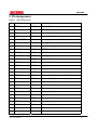
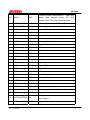
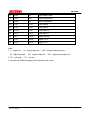
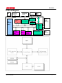
MD-6002
DATA SHEET
MD-6002
USB2.0 Flash Disk Controller
Revision 1.3
Copyright © 2007 MoreDNA Technology Co.,Ltd..
Ver1.3 5/30/2008
1
MD-6002
1. General Description
MD6002 is a high-performance integrated circuit to access the Data Flash memory via the
480 MHz USB 2.0 bus. It provides a flexible and cost efficient single chip solution for external
storage applications such as USB Disk (Flash Disk) and fingerprint interface. With all the
features inherited from the popular MD6001, the users can easily upgrade to MD6002 and
enjoy the tremendous speed increment.
Although the USB speed is increased 40 times from 12 M to 480 M, the external crystal
frequency of MD6002 is still kept at 12MHz, keeping the EMI at low level. The functions that
ensure the data integrity like the embedded translation table, the MoreDNA
proprietary
randomization algorithm, and the real time ECC correction function are all the implemented as
the USB 1.1 version. MD6002 also incorporates MoreDNA in-house algorithm to improve the
performance of the flash disk.
To enrich the product line of the OEM manufacture and reduce the effort of component
sourcing, MD6002 supports both single channel and dual channel modes in a single chip. In
addition, MD6002 supports NAND flash memories of Samsung, Toshiba, Hynix,
STMicroelectronics , Micron and, providing more flexibility for the flash memory’s purchasing
and Toshiba/ Hynix MLC flash memories.
With the ability to support 8 pieces of flash memories and the new types of 2Gb, 4Gb, 8Gb,
16Gb and 32Gb bits flashes, MD6002 can be used to build up a storage device up to 16 Giga
bytes large.
The USB Mass Storage Class compliance capability of MD6002 makes it a truly
“plug-and-play” device without vendor drivers under Windows Vista/2000/ME/XP and WIN-CE,
Mac OS 8.6/9/10, and Linux. MD6002 also provides PC boot up function as a USB ZIP, USB
HDD or USB CD-ROM, which makes it an ideal replacement for the legacy floppy disk.
Ver1.3 5/30/2008
2
MD-6002
2. Features
z
USB 2.0 480 MHz high-speed compatible
z
USB 1.1 Mass Storage Class compliant
z
USB Mass Storage Class Bulk-Only Transport 1.0 supported
z
USB Mass Storage Class SCSI transparent command set supported
z
Low system clock (12MHz) to reduce EMI
z
Customized USB VID, PID, serial number, and USB vendor/product strings
z
28 characters of Vendor/Product/Revision string supported for each LUN separately
z
Support Samsung and Toshiba NAND-type flash memory, from 32Mbits to 1Gbits
z
Support new type of Samsung NAND type flash memory, from 1Gbits to 32Gbits
z
Support Hynix /STMicroelectronics/Micron flash memories
z
Support Toshiba / Samsung /Hynix MLC flash memories
z
Support ZIP/HDD/CD-ROM format through MoreDNA mass production tool
z
Support Autorun function (Optional)
z
Support CD-RW function (Optional)
z
Real-time ECC correction circuit for data integrity and memory access speed acceleration
z
Embedded SRAM for logical-to-physical address translation to extend the life time of
NAND-type flash
z
Support up to 8 NAND type flash memories are supported (single channel mode)
z
Support dual channel mode for speed improvement
z
Support up to 16G bytes of disk capacity
z
Embedded FIFO for upstream and downstream data transfer
z
Built-in power MOS to meet USB suspend requirement (500 uA)
z
Data transfer rate up to 60MB/s (burst)
z
LED indicator pin
z
Three modes of LED flashing patterns can be selected
z
Five speed of LED flashing speed provided
z
PC boot up capability (host BIOS with USB boot up support is necessary)
z
Flash disk security function provided, up to 16 characters of password for high sensitive
data protection from illegally access
z
Most security features can be accessed by the administrator mode and the user mode
under Microsoft Windows. (Optional)
Ver1.3 5/30/2008
3
MD-6002
z
Five types of security functions can be selected
z
Ten types of sensor can be selected
z
ROM-type flash disk capability provided (permanent write protect)
z
Different LUN can be set to write protect separately
z
No driver needed under Microsoft Windows Vista/ME/2000/XP, Mac OS 8.6/9.x/10.xNo
driver needed for Linux kernel 2.4 or above
z
MoreDNA Driver for Microsoft Windows 98/98SE
z
MoreDNA mass production tool available for mass production (under win2k/xp)
z
MoreDNA utility program available (under Windows and Mac 10.2 or above)
z
MoreDNA driver and utility program available (under Mac 9, version 9.1 or above)
z
Signal Voltage 3.3V operation (input)
z
64 pin LQFP package
Ver1.3 5/30/2008
4
MD-6002
3. Pin Assignment
Table 1
MD-6002 pin list
NO pin name
type
description
1
VDD33
PWR
Digital 3.3V
2
LED
DO
LED output
3
GPIO4
DIO
General purpose input/output 4
4
INT
DI
External Interrupt input
5
GPO5(F_CE5)
DO
General purpose output 5/ flash chip enable 5
6
VDDA
PWR
Analog 3.3V
7
RPU
AIO
Connect to 1.5K pull up resistor
8
DPLUS
AIO
USB D+
9
DMINUS
AIO
USB D-
10
VSSA
PWR
Analog ground
11
VDD33
PWR
Digital 3.3V
12
VDD18
PWR
Digital 1.8V
13
VSSD
PWR
Digital ground
14
VDDA
PWR
Analog 3.3V
15
VSSA
PWR
Analog ground
16
VRES
AIO
Reference voltage, connect to 6.2K resistor
17
FLD15
DIO
Flash data 15
18
FLD0
DIO
Flash data 0
19
FLD1
DIO
Flash data 1
20
XOUT
DO
Crystal output
21
XIN
DI
Crystal input
22
VD33
PWR
Digital 3.3V
23
VD18
PWR
Digital 1.8V
24
VSS
PWR
Digital ground
25
FLWE
DO
Flash write enable
26
FLALE
DO
Flash address latch enable
27
FLD2
DIO
Flash data 2
Ver1.3 5/30/2008
5
MD-6002
General purpose input/output 0 / flash chip
28
GPIO0
DIO
enable (dual channel mode), PU: dual
channel mode, PD: single channel mode
29
GPO6(F_CE6)
DO
General purpose output 6/ flash chip enable 6
30
GPO7(F_CE7)
DO
General purpose output 7/ flash chip enable 7
31
VD33
PWR
Digital 3.3V
32
FLCE0
DIO
Flash chip enable 0
33
FLD3
DIO
Flash data 3
34
GPIO5
DIO
General purpose input/output 5
35
FLCE2
DIO
Flash chip enable 2
36
VD33
PWR
Digital 3.3V
37
FLCLE
DO
Flash command latch enable
38
FLD4
DIO
Flash data 4
39
FLD5
DIO
Flash data 5
40
FLD12
DIO
Flash data 12
41
FLD6
DIO
Flash data 6
42
VSS
PWR
Digital ground
43
VD18
PWR
Digital 1.8V
44
VD33
PWR
Digital 3.3V
45
FLRE
DO
Flash read enable
46
FLD13
DIO
Flash data 13
47
FLD7
DIO
Flash data 7
48
FLCE1
DIO
Flash chip enable 1
49
FLD14
DIO
Flash data 14
50
FLCE3
DIO
Flash chip enable 3
51
GPO4(F_CE4)
DO
General purpose output 4/ flash chip enable 4
52
VSS
PWR
Digital ground
53
FLWPSW(GPIO3) DI
54
VD33
Ver1.3 5/30/2008
PWR
Write protect switch input/ General purpose
input /output 3
Digital 3.3V
6
MD-6002
55
RSTN
DI
Chip master reset
56
FLWP
DO
Flash write protect
57
FLRB1
DI
Flash ready/busy
58
FLD8
DIO
Flash data 8
59
FLD9
DIO
Flash data 9
60
FLD10
DIO
Flash data 10
61
FLD11
DIO
Flash data 11
62
VSS
PWR
Digital ground
63
VD18
PWR
Digital 1.8 V
64
VD33
PWR
Digital 3.3V
Note:
1. P:power pin; AI:analog input pin; AIO:analog input/output pin;
DI:digital input pin; DO:digital output pin; DIO:digital input/output pin.
2. PD:pull down; PU:pull up.
3. All pads are Schmitt triggered and with slew rate control
Ver1.3 5/30/2008
7
MD-6002
4. Block Diagram
SPI
Two-wires
interface
Fingerprnt
sensor
USB
Interface
GPIO
Ports
MD600X
MCU
(E8051D)
Code/Data
SRAM 2
KB
Fingerprint
ACC engine
USB2.0
Transceiver
60MHz
Private
Encryption
MAC
Ver1.3 5/30/2008
RNG
(ANSI
X9.31)
ROM code
64 KB
(MASK) .
FIFO
USB2.0
Controller
NAND
Flash
Memory
Slave
FIFO
I/F
LBA Interface
LBA
Memory
8
MD-6002
5. Functional descriptions
5.1 Flash memory connection
In single channel mode, up to 8 NAND type flash memories can be connected to MD6002 (in
dual channel mode, only 2 flash memories can be connected), the number of flash memory
connected can be detected automatically upon power on. Each flash memory has its own chip
enable control signal path (FLCE 1 to FLCE8). All flash memories connected to MD6002 must
be of the same capacity. There is no special rule for the number of flash memory. (e.g. not
necessarily to be the multiples of 2 or 4).
5.2 USB VID/PID/SN and Strings format
The USB vendor ID, product ID, serial number, and the strings can be changed by using the
MoreDNA Mass Production tool. The vendor name and product name of each LUN can also be
changed. The serial number (defined in mass storage device class) can also be customized or
disabled. It should be noted that the VID and PID values cannot be set to 0x0000 or 0xFFFF or
any value that reserved by the USB standard. If there is no customized VID/PID, default USB
vendor ID (hex 0C45) and product ID (hex 2060) are returned to the host. For detail, please
refer to the user’s manual of MD6002 mass production tool.
Ver1.3 5/30/2008
9
MD-6002
5.3 Fingerprint sensor support
The MD6002 can support 7 brand sensor, and 10 kinds sensor.
1.
Authentec
2.
ATMEL
3.
ATRUA
4.
LighTuning
5.
MITSUMI
6.
Pixart
7.
SOI
MoreDNA provides the following software to customers.
Please contact the sales for detail.
1)
Application software and driver for Win98/2000/Me/XP/Vista; boot up utility is included for
Win98/Me
2)
Application software and driver for Mac OS9 (version 9.1 or above)*
3)
Application software for Mac OS 10.2 or above*
4)
Mass production tool under Win2000/XP/Vista
5)
Fingerprint Application software for Win98/2000/Me/XP/Vista;
* The functions of the application software between different OS might be different
Ver1.3 5/30/2008
10
MD-6002
6. Operating rating and electrical characteristics
6.1 Absolute maximum rating
Table 2
symbol
Parameter
value
unit
Dvmin
min digital supply voltage
DGND – 0.3
V
Dvmax
max digital supply voltage
DGND + 3.6
V
Avmin
min analog supply voltage
AGND – 0.3
V
Avmax
max analog supply voltage
AGND + 3.6
V
Dvinout
voltage on any digital input or output pin DGND –0.3 to 3.6
Avinout
Tstg
voltage on any analog input or output
pin
storage temperature range
V
AGND –0.3 to Avdd + 0.3 V
-40 to +125
0
C
ESD human body mode
ESD (HBM)
C=100pF, R=1.5KΩ
2000
V
ESD (MM)
ESD machine mode
200
V
Ioff
leakage current
10
uA
Ilatch
minimum latch up current
100
mA
6.2 Operation conditions
Table 3
symbol
Parameter
value
unit
DVdd
digital supply voltage (3.3V)
+3 to +3.6
V
DVddL
digital supply voltage (1.8V)
+1.62 to +1.98
V
Avdd
analog supply voltage (3.3V)
+3 to +3.6
V
AvddL
analog supply voltage (1.8V)
+1.62 to +1.98
V
TA
operating ambient temperature range
0 to 70
0
TJ
operating junction temperature range
0 to 115
0
Ver1.3 5/30/2008
C
C
11
MD-6002
6.3 DC electrical characteristics
Table 4
symbol
parameter
test condition
value
unit
V
USB full speed differential input
| (D+) – (D-) |
0.2 (min)
V
V
sensitivityUSB full speed
Included V
0.8 (min)
V
differential common mode range
range
DI
CM
V
DI
2.5 (max)
USB high speed squelch
100 (min)
detection threshold
150 (max)
USB high speed disconnect
525 (min)
detection threshold
625 (max)
USB high speed data signaling
-50 (min)
common mode voltage range
500 (max)
V
dttithhld high level input voltage
2.0 (min)
V
V
low level input voltage
0.8 (max)
V
V
high level output voltage
I
2.3 (min)
V
V
low level output voltage
I = 4 mA
0.5 (max)
V
I
low level input current
V =0V
RSTN pin :z - 50.0 (max)
μA
HSSQ
V
HSDSC
V
HSCM
IH
IL
OH
OL
IL
OH
= -4 mA
OL
I
mV
mV
mV
the other pins : - 3.0 (max)
I
high level input current
V = 3.6 V
3.0 (max)
I
input supply current
20 (max)
mA
Isuspend
supply current in suspend
350 (max)
μA
IH
DD
I
μA
6.4 AC electrical characteristics
6.4.1 USB transceiver signal (full speed mode)
Table 5
symbol
parameter
Tr
min
max
unit
transition rise time for DP or DM
4
20
ns
Tf
transition fall time for DP or DM
4
20
ns
Trfm
rise / fall time matching
90
111.11
%
1.3
2.0
V
Vo(crs) signal crossover voltage
Ver1.3 5/30/2008
test condition
(Tr / Tf ) * 100
12
MD-6002
6.4.2 USB transceiver signal (high speed mode)
Table 6
symbol parameter
test condition
min
max
unit
Thsr
transition rise time for DP or DM
0.5
ns
Thsf
transition fall time for DP or DM
0.5
ns
6.4.3 Operation clocks
Table 7
symbol
parameter
value
unit
USBCLKin
XI/XOUT crystal value
12 (typ)
MHz
USBCLKin duty cycle
50 ± 2
%
6.5 Power consumption
Table 8
symbol
parameter
value
unit
Io_max
Max current in operation
80
mA
Is_max
Max current in suspend mode
TBD
uA
Ver1.3 5/30/2008
13
MD-6002
7. Packaging dimension
Ver1.3 5/30/2008
14