1
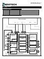
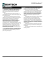
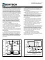
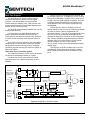
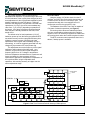
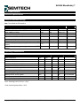
SH3000 MicroBuddy™
Low-Power Programmable Multifunction
Support IC for Microcontrollers
SYSTEM MANAGEMENT
Description
Features
The programmable SH3000 MicroBuddy™ (µBuddy™)
provides all mandatory microcontroller support functions:
♦
♦ CPU Supervisor
♦ Clock Management System
♦ Real Time Support
♦ Auxiliary functions
Three components make a complete system: any
microcontroller, the SH3000, and a bypass capacitor.
This low-cost system would consume very little power and
have clock-frequency accuracy of ±0.5%. A fourth
component, a 32.768 kHz watch crystal, raises the clock
frequency accuracy to ± 0.0256% (± 256 ppm).
The SH3000 can operate completely stand-alone, or
under control of the microcontroller. A single-wire
interface handles both bi-directional communications and
the interrupt / wake-up signal from the SH3000. The
SH3000 stores all configuration, calibration, parameters,
and status information in a 36-byte bank of control
registers. On reset, most of these are reloaded with
defaults from the factory-set One-Time-Programmable
(OTP) memory. The microcontroller can change any
settings on the fly. If some of the settings must remain
fixed, a comprehensive set of write-protect bits is provided
for several related groups of registers (with both
permanent write-inhibit and lock/unlock capabilities).
A backup power source may also be connected to the
SH3000. The IC can directly accommodate 2/3-cell zinccarbon/alkaline, 2/3-cell mercury, 2/3/4-cell NiCd/NiMH, 1cell Li/Li+ batteries, or a super cap.
♦
♦
♦
♦
♦
♦
♦
♦
Highly integrated IC
- 3mm x 3mm x 0.9 mm 16-lead MLP (QFN) package
CPU Supervisor
- Low VDD reset programmable from 2.3 V to 4.3 V
- Watchdog timer with programmable timeout periods
- Both active-high and active-low reset outputs
Clock Management System
- Replaces High-Frequency (HF) crystal or resonator
- Programmable clock output from 32 kHz to 16 MHz
- Speed shift between multiple clock frequencies
- Adjustable spectrum spreading for EMI reduction
- Directly supports microcontroller STOP function
- Deep sleep with instantaneous auto-wakeup
Real Time Support
- 179-year real time clock, battery backup capable
- Dedicated 32 kHz buffered clock output
- Built-in trim for 32.768 kHz oscillator to ± 4ppm
- Programmable periodic interrupt / wakeup timer
Auxiliary functions
- 4-byte (32-bit) scratchpad RAM, loaded on reset with
factory-set value (zero or optional ID code)
- All settings programmable in real-time, defaults
restored from OTP memory on reset
Operates from 2.3 V to 5.5 V
IDD <850µA / 2MHz, <3mA / 16MHz, <10µA/standby
IBUP <2µA / IBSB <50nA (battery backup / standby)
Protected by issued and pending
US and International Patents
GPIO WITH INT
16
15
14
13
NRESET
µBTM
SH3000
12
11
10
9
µController
GND
VDD
3
VBAK
4
IO/INT
CLK32
14
13
µBTM
12
TEST (VSS)
11
RST
10 NRST
SH3000
9
5
6
7
RREF
8
3mm MLP (QFN) Package
5
6
7
8
1
2
3
4
VREG
2
15
VSS
XIN
XOUT
1
16
CLKSEL
VDD
CBYPASS
VSS
CLKIN
Home automation and security
Consumer products
Portable/handheld computers
Industrial equipment
Any microcontroller-based product
V+
XOUT
♦
♦
♦
♦
♦
XIN
Applications
CLKOUT
Pin Configuration
Typical Application Circuit with High Clock Accuracy
2005-08-08
Copyright ©2003-2005 Semtech Corporation 1
Covered by US Patent No. 6,903,986
Semtech, the Semtech logo, MicroBuddy, µBuddy, and µB are marks of
Semtech Corporation. All other marks belong to their respective owners.
V1.15 www.semtech.com
SH3000 MicroBuddy™
SYSTEM MANAGEMENT
Description
Ordering Information
SH3000IMLTR
SH3000IMLTRT
EVK-SH3000USB
SH3000EK.pdf
SH3000UM.pdf
IC
IC
Evaluation kit
Evaluation kit user manual
User manual
MLP 3 x 3 mm 16 pins, -40° C to +85° C
MLP 3 x 3 mm 16 pins, -40° C to +85° C, Lead Free
Block Diagram
Microcontroller
VDD
32KHZ
XIN
XOUT
RESET
I/O PIN
16
CLKIN
13
CLKOUT
3
CLK32
2
VDD
VREG
V+
15
VBAK
4
Regulators &
Battery Back-up
Clock Driver &
Start/Stop Logic
VSS
Post-scaler
1
HF Oscillator
& FLL
Voltage
Reference
VSS
8
XIN
LF Oscillator
5
XTAL
Oscillator
XOUT
6
CLKSEL
7
RREF
9
OTP Memory
Calibration &
Default Settings
RST
VDD Monitor
Reset Drivers
& Logic
NRST
10
Watchdog
Control Logic
Real Time Clock
Select
Logic
11
Periodic Interrupt
/ Wake-up Timer
RC
Oscillator
Interrupt
Serial I/O
TEST
12
IO/INT
14
SH3000 µBuddy™
Copyright ©2003-2005 Semtech Corporation
2
V1.15
www.semtech.com
SH3000 MicroBuddy™
SYSTEM MANAGEMENT
Pin Descriptions
Pin
Name
Type
Function
1
VSS
Power
2
VREG
Power
3
VDD
Power
4
VBAK
Power
5
XIN
Analog In
6
XOUT
Analog Out
7
CLKSEL
Digital In
8
VSS
Power
9
RREF
Analog
10
NRST
Digital Out
11
RST
Digital Out
Ground, 0 V. All VSS pins and TEST (VSS) pin must be connected together.
Output of internal Voltage Regulator, 2.2 V nominal. This pin can power external loads
of <5 mA. If load is “noisy” it requires a bypass capacitor. May be left unconnected or
used as a high logic level signal for CLKSEL pin (see below).
Main power supply, +2.3 to +5.5 V.
Backup power supply for real time clock, +2.3 to +5.5 V (+1.8 to +5.5 V typical). This
voltage can be higher or lower than VDD. Connect a backup battery or backup
capacitor (with external recharge circuit). Connect to VDD if not used.
Oscillator pins for optional external low frequency crystal, typically 32.768 kHz watch
crystal with nominal 12.5 pF load capacitance. Keep open or connect to VSS if not
used.
A logic low level selects the internal 32 kHz RC oscillator (CLKSEL tied to VSS). A high
state on this pin selects the 32 kHz crystal oscillator (CLKSEL is connected to VREG).
The SH3000 always starts up using the internal 32 kHz RC oscillator. If CLKSEL is
high, the internal 32 kHz clock switches to the crystal oscillator once it has stabilized,
and RC oscillator is disabled for power conservation.
Do not connect CLKSEL to any signals except VSS or VREG. CLKSEL must not be left
open.
Ground, 0 V. All VSS pins and TEST (VSS) pin must be connected together.
Optional 1MOhm external bias resistor for the internal 32 kHz RC oscillator. Can be
used to set, trim or modulate the internal RC oscillator. Keep open if not used.
Active low system reset output. Asserted with a strong low state when a reset condition
occurs. Weakly pulled to VDD internally when not active. This signal is valid for VDD as
low as 1 V. Keep open if not used.
Active high system reset output. Asserted with a strong high state when a reset
condition occurs. Weakly pulled to VSS internally when not active. This signal is valid
for VDD as low as 1 V. Keep open if not used.
Factory test enable. All VSS pins and TEST (VSS) pin must be connected together.
Buffered internal 32 kHz clock, derived according to the CLKSEL pin setting. This pin
uses backup power for the buffer when VDD is not present. When driving high, this signal
is either at VBAK or VDD (if VDD is higher than the reset threshold). When enabled, this
signal runs continuously independent of CLKOUT activity. Minimize the external load to
reduce power consumption during backup operations. When disabled, this pin is driven
to VSS. Keep open if not used.
Serial communications interface and interrupt output pin. This pin is internally weakly
pulled to the opposite of the programmed interrupt polarity. For example, if interrupt is
programmed to be active low, this pin is weakly pulled to VDD when inactive. Keep
open if not used.
Clock activity sense input. Used to detect when the target microcontroller enters stop
mode (which disables its clock). Connect to the microcontroller’s clock output or
oscillator output pin. Connect to VSS when not used. CLKIN must not be left open.
Programmable high frequency clock output. Connect to the target microcontroller’s clock
input or oscillator input pin. Keep open if not used.
12 TEST (VSS)
Digital In
13
CLK32
Digital Out
14
IO/INT
I/O
15
CLKIN
Digital In
16
CLKOUT
Digital Out
Copyright ©2003-2005 Semtech Corporation
3
V1.15
www.semtech.com
SH3000 MicroBuddy™
SYSTEM MANAGEMENT
The SH3000 is a particularly desirable integration
because the built-in features interact and meld to
produce more useful system level functions.
For example, on power up, the SH3000 can quickly
release the reset lines on its CPU Supervisor module
because the clock signal from the Clock Management
System is guaranteed to be running and stabilized. An
ordinary reset circuit must hold reset active for a long
time to allow an unknown crystal to start up and
stabilize.
The SH3000 offers several ways to minimize system
power consumption, such as allowing the target
processor to enter deep sleep by stopping its clock
completely, and to wake up as often as necessary with
no external support. The clock can be programmed to
start up at a given frequency, and software can adjust it
dynamically to manage power consumption and different
operating modes.
Users should consider the interactions of the major
functional blocks to gain the maximum advantage from
the SH3000.
The individual functional blocks are described in the
following sections.
Functional Description
The SH3000 is a single-chip support system for
microcontrollers, microprocessors, DSPs and ASICs. It
consists of four major functional blocks, each block
having numerous enhancements over alternative
solutions.
The major modules are the CPU Supervisor, the
Clock Management System, the Real Time Support, and
the Auxiliary functions.
The entire chip is controlled by the set of internal
registers and accessed via the single-pin serial interface.
All of the settings, configuration, and calibration or
operating parameters are programmable and reprogrammable at any time. All of the parameters
required for stand-alone operations are initialized on
reset from the built-in factory-programmed OTP
nonvolatile memory. This allows the SH3000 to operate
autonomously for most of its supervisory functions. The
stand-alone operations do not require the use of the
serial interface or any of the initialization and control
operation, but without these, the full potential benefit of
the SH3000 may not be realized.
In the preferred configuration, where the SH3000 is
tightly coupled to the target micro, the SH3000 offers an
unprecedented level of design flexibility in clock and
power usage management.
Copyright ©2003-2005 Semtech Corporation
4
V1.15
www.semtech.com
SH3000 MicroBuddy™
SYSTEM MANAGEMENT
The default VBO value is loaded on power-up from
the factory-programmed OTP nonvolatile memory. It
can be re-programmed at any time or it can be
permanently protected from any changes by setting the
VBO Lock flag or an OTP write-protect flag.
On power up both the active-high and active-low
reset signals are driven active. These outputs are
typically valid for a VDD level of at least 0.5 V, and
guaranteed to be valid for a VDD level of 1.0 V.
The reset outputs remain active until VDD rises and
stays above the level of (VBO + VHYST), where VHYST is
a small fixed amount of hysteresis, nominally 50 mV,
added to prevent nuisance reset activations (when VDD
slowly changes near the level of VBO and some noise or
power glitching is present).
At the level of (VBO + VHYST) the power supply is
considered valid. In case of the initial power-up, the
reset is then driven inactive once 6 ms of valid power
have elapsed. In the case of brownout, the reset is
released after a delay of 6 ms (but no less than 12 ms
from the beginning of the brownout).
Such a fast reset is possible because the SH3000
provides a fast-starting clock that is free of crystal startup time requirements. This gives the SH3000 an
advantage over most external reset circuits, which must
have a long reset pulse duration to accommodate long
and unpredictable crystal start-up times.
The SH3000 guarantees that a valid and stable
clock is available 2 ms before the reset signals are
negated, so that internal synchronous reset and
initialization of the target micro can proceed normally.
CPU Supervisor
The SH3000 has two supervisory functions that
manage the reset of the target processor, a low VDD
monitor (Brownout Detector) and a Watchdog Timer, see
Figure 1.
Both functions are integrated with the Clock
Management System to provide a more complete
system solution than the stand-alone components.
The SH3000 has both active high and active low reset
output pins. Both are driven strong to the active state
and weak to the inactive state. This eliminates the need
for external pull-ups and allows various reset sources to
be connected together in a wire-OR configuration. (This
makes it simple to set up a manual reset circuit.)
A set of flags in the register map indicates the
source of the reset to the system software.
Low VDD Reset
The SH3000 drives the reset pins active whenever
VDD is below the value of VBO, the brownout reset
threshold, programmable from 2.3 V to 4.3 V in average
steps of 33 mV, see Table 1.
Table 1. Programmable VBO Values
Parameter
Min
Typ
VBO for min code
2.27
2.3
(000000)
VBO for max code
4.2
4.3
(111111)
Step resolution
25
33
VDD
Max
2.33
Units
V
4.4
V
41
mV
RESET
Noise Filter
32kHz
1
PWROK
Lock Logic
2.30 V
VLOW
D/A
6-bit Value
CLKOUT
Hysteresis
50mV TYP.
÷ 256
32kHz
Write-once
Initialization Logic
RST
VDD
20K
11
20K
UNDERFLOW 1→0
RESET
Temperature- 4.40 V VHIGH
compensated
Threshold
Voltage
Reference
Reset Logic
&
Minimum
Duration Timer
10
7-bit Down Counter
÷ 128
Load
Mode
NRST
7-bit Watchdog
Timeout Value
Watchdog
Reload Control
Alternating Codes
Logic
0x5A / 0xC3
From / To
Serial I/O
Figure 1. CPU Supervisor --- Low VDD / Brownout Detector, Watchdog, Reset logic & Drivers
Copyright ©2003-2005 Semtech Corporation
5
V1.15
www.semtech.com
SH3000 MicroBuddy™
SYSTEM MANAGEMENT
Since the clock is only active for the last 1 or 2 ms of
the reset interval, when VDD has already been valid for
some time, energy savings are realized and the startup
of the whole system is made easier. Commonly used
reset approach forces the processor to turn the oscillator
on and to run at full speed (thus consuming full power)
during the critical time when (possibly depleted) battery
is trying to raise VDD to an acceptable level. In contrast,
the SH3000 allows the power source to charge the
bypass capacitors and raise the level of VDD with little
additional load. Only when power has stabilized is the
target micro permitted to start expending energy.
When a brownout event occurs, the SH3000
continues to provide the clock to the target processor,
but at a reduced frequency between 500 kHz and
1.0MHz. After a delay of 2 ms this clock is stopped,
automatically lowering the energy consumption of the
whole system, see Figure 2.
A Noise Filter (see Figure 1) prevents reset
activations from noise and small power glitches on the
VDD line. A typical behavior is shown in Figure 3 for the
VDD level just above VBO and various amplitudes and
durations of the negative-going spikes.
When VDD is falling, both reset lines are guaranteed
to activate within 5 µs from the time VBO is crossed over.
Watchdog Timer
The second circuit for supervising the processor is
the watchdog timer. Whereas the low VDD / Brownout
Detector monitors supply voltage, the watchdog timer
monitors behavior. It is based on a programmable timer
that must be restarted periodically by the host micro. If
software fails to restart the timer, the watchdog resets
the processor.
Restarting the timer takes considerable processing,
making it unlikely that it would occur accidentally, as
might happen for a simple pin-strobe configuration of a
typical watchdog IC.
The watchdog is disabled after reset occurs. It stays
disabled until initialized by the host processor.
The initialization requires the watchdog clock mode
to be selected (see Figure 1) and the 7-bit time-out
value to be set. As soon as the time-out is written, the
watchdog begins operations and can not be stopped;
also, the time-out value and or clock source can no
longer be changed.
The two clock sources available for the watchdog
are the internal 32 kHz clock and the CLKOUT signal.
When operating from the 32 kHz source, the timeout interval is programmable from 7.8125 ms to
1 second with resolution of 7.8125 ms. Internal 32 kHz
clock is running all the time, therefore the time-out
duration is fixed and predictable.
When operating from the CLKOUT signal the time-out
interval is programmable between 256 and 32768 cycles
of CLKOUT with resolution of 256 cycles. The actual
time-out duration is variable and depends both on the
frequency of CLKOUT signal and the amount of time the
target micro spends in the STOP mode, when the
CLKOUT signal is also stopped.
These two clock modes, together with the
programmable time-out value, allow the SH3000
exceptional flexibility, previously unattainable by existing
discrete watchdog solutions.
12ms minimum
VBO + VHYST
1V
6ms
Duration, µs
3-5ms
Amplitude
VDD
Duration
10
VBO
RST
Undefined
5
Guaranteed reset
NRST
1ms
CLKOUT
Normal
FOUT
2ms
Guaranteed NO reset
2ms
0
0.05 0.1 0.15 0.2 0.25 0.3 0.35 0.4 0.45 0.5
Reduced FOUT
0.5-1.0 MHz
Am plitude, V
Figure 2. Operations of low VDD / Brownout Detector
Copyright ©2003-2005 Semtech Corporation
Figure 3. Response to negative voltage spikes
6
V1.15
www.semtech.com
SH3000 MicroBuddy™
SYSTEM MANAGEMENT
The watchdog timer is kept from timing out by
periodic reload of the time-out value, triggered by a write
of a code byte to the Watchdog Reload Register. As a
further safety measure, there are two different and
alternating code bytes that should be written to the same
Watchdog Reload Register. The code values are 0x5A
and 0xC3. The timer is reloaded after every write of a
single code byte.
The code byte should be written to the Watchdog
Reload Register, or reset is activated when the
watchdog timer expires. Also, reset is initiated
immediately if the value of the code byte is incorrect or
out of sequence. When the watchdog triggers the reset,
its duration is 12 ms.
Using two separate software routines, each to write
one of the code values, results in the highest level of
system security. These routines must execute in the
correct order. It is unlikely that runaway code could
manage this. In addition, this design makes it difficult for
the code to become stuck in a tight loop resetting the
watchdog.
The SH3000 permits the automatic sensing of the
intentions of the host processor, an industry first. The
SH3000 shuts down its clock output when it senses that
the host processor issued a STOP instruction.
Subsequently, the SH3000 idles, consuming less than
10 µA. As soon as the host exits the STOP mode, the
SH3000 instantaneously starts to supply a stable clock
(<2µs wake-up).
A typical system, constructed with a ceramic
resonator or a crystal as the frequency determining
element, must wait at least several hundred
microseconds (for a resonator), or as much as 100 ms or
more (for a HF crystal), to re-start the oscillator. The
SH3000 allows the response to and service of an event
to finish with a speed previously unattainable for a
simple microprocessor. A system with a traditional clock
approach may be as much as 100x – 10,000x slower.
Clock Generator Operation
The frequency synthesizer in the SH3000 is
constructed from the 2:1 tunable 8.0 –16.0 MHz HF
oscillator followed by a programmable “power-of-two”
post-divider (see Figure 4).
The Clock Source selector and the programmable
post-scale divider allow instantaneous switching
between the 32 kHz internal clock and divided-down HF
oscillator output. There is no settling or instability when
the switch occurs.
This is a preferred method for clock control in
computing systems, when the large ratio between high
and low frequency of operations allows for
correspondingly large and instantaneous savings in
power consumption.
Clock Management System
The SH3000 provides a flexible tool for creating and
managing clocks, a versatile and accurate “any
frequency” clock synthesizer (see Figure 4).
It is capable of generating any frequency in the
range of 62.5 kHz to 16.0 MHz, with worst-case
resolution of 0.0256% (256 ppm). The internal 32 kHz
clock can also be routed to the CLKOUT pin (and HF
oscillator stopped for energy savings).
The objectives, features, and behavior of the Clock
Management System are aimed towards the systems
that utilize a microcontroller, a microprocessor, a DSP or
an ASIC.
Clock Source
1
32.768 kHz
Post-scaler
(Divide by 1, 2, 4,
8, 16, 32, 64, 128)
FLL On
0
Clock On
CLKOUT
Clock Buffer
and Glue
Logic
16
CLKIN
15
START/STOP
÷ 16
2048 Hz
Frequency Locked Loop
Logic
13-bit
Frequency
Set value
From / To
Serial I/O
18-bit
DCO Code
Register
8-bit Pseudo
Random Noise
Generator
HF Digitally
Controlled
Oscillator
8-16 MHz
Force
DCO On
Spectrum
Spreading
Controls
Figure 4. Simplified HF Oscillator System
Copyright ©2003-2005 Semtech Corporation
7
V1.15
www.semtech.com
SH3000 MicroBuddy™
SYSTEM MANAGEMENT
When the HF oscillator is operating alone, it can set
the frequency of the clock on the CLKOUT pin to
±0.025%, and maintain it to ±0.5% over temperature.
This compares favorable with the typical ±0.5% initial
clock accuracy and ±0.6% overall temperature stability
of ceramic resonators. The SH3000 replaces the typical
resonator, using less space and providing better
performance and functionality.
The HF oscillator can also be locked to the internal
32 kHz signal. The absolute accuracy and stability of
the HF clock depends on the quality of the 32.768 kHz
internally generated clock; the low-frequency (LF)
Oscillator System is described later in this document.
When the Real Time Clock module of the SH3000 is
used for high-accuracy timekeeping, an external 32.768
kHz watch crystal used as a reference for RTC provides
excellent accuracy and stability for the Clock
Management System.
The SH3000 employs a Frequency Locked Loop
(FLL) to synchronize the HF clock to the 32 kHz
reference. This architecture has several advantages
over the common PLL (Phase Locked Loop) systems,
including the ability to stop and re-start without
frequency transients or instability, and with instant
settling to a correct frequency. The conventional PLL
approach invariably includes a Low-Pass Filter that
requires a long settling time on re-start.
Copyright ©2003-2005 Semtech Corporation
The primary purpose of the FLL is the maintenance
of the correct frequency while the ambient temperature
is changing. As the temperature drift of the HF oscillator
is quite small, any corrective action from the FLL system
is also small and gradual, commensurate with the
temperature variation.
The FLL system in the SH3000 is unconditionally
stable.
To set a new frequency for the FLL, the host
processor writes the 13-bit Frequency Set value. The
resulting output frequency is calculated using simple
formulas [1] and [2] (reference frequency is 32.768 kHz):
FOSC = 2048 Hz * (Frequency Set value + 1) [1]
FOUT = FOSC / (Post-divider setting) [2]
For example, a post-divider setting of ÷8 and the
Frequency Set value of 4000 (0x0FA0) produce an
output frequency of 1.024 MHz.
8
V1.15
www.semtech.com
SH3000 MicroBuddy™
SYSTEM MANAGEMENT
Programmable Spectrum Spreading
Most commercial electronic systems must pass
regulatory tests in order to determine the degree of their
Electromagnetic Interference (EMI) affecting other
electronic devices. In some cases compliance with the
EMI standards is costly and complicated.
The SH3000 offers a technique for reducing the
EMI. It can be a part of the initial design strategy, or it
can be applied in the prototype stage to fix problems
identified during compliance testing. This feature of the
SH3000 may greatly reduce the requirements for
radiofrequency shielding, and permits the use of simple
plastic casings in place of expensive RFI-coated or
metal casings.
The SH3000 employs Programmable Spectrum
Spreading in order to reduce the RF emissions from the
processor’s clock. There are five (5) possible settings;
please see Table 3 for operating and performance
figures in the 8-16 MHz range.
Special Operating Modes
The SH3000 can operate stand-alone, without
connections to the In and Out terminals of the host’s
oscillator. For example, a bank of SH3000 chips can
generate several different frequencies for simultaneous
use in the system, all controlled by a single micro (and
possibly sharing one 32.768 kHz crystal by chaining the
CLK32 pin to XIN pin on the next device). In this case
the CLKIN pin should be connected to VSS. The clock
output on the CLKOUT pin is continuous; the correct
operating mode is automatically recognized by the
SH3000.
Likewise, a microcontroller may not have a STOP
command at all. Still, with the help of the SH3000 this
controller can do a “simulated” STOP by issuing an
instruction to the SH3000 to stop the clock. This
command is accepted only if the Periodic Interrupt /
Wakeup Timer has started (otherwise, once the system
is put to sleep, it would never wake up again). This
mode of operations is only possible if the host processor
is capable of correct operations with clock frequency
down to zero, and keeps all of the internal RAM alive
while the clock is stopped.
Table 3. EMI reduction with Spectrum Spreading
Spreading Peak EMI Peak EMI
Bandwidth Reduction Reduction
Setting
(guaranteed) (measured)
db
db
En
0
CFG1
X
CFG0
X
kHz
Off
0
0
1
0
0
32
-3
-3
1
0
1
64
-6
-7
1
1
0
128
-9
-10
1
1
1
256
-12
-15
Spectrum Spreading is created by varying the
frequency of the HF oscillator with a pseudo-random
sequence (with a zero-average DC component). The
Maximum-Length Sequence (MLS) 8-bit random number
generator, clocked by 32 kHz, is used. Only 4, 5, 6, or 7
bits of the generated 8-bit random number are used,
according to the configuration setting.
Maximum fluctuations of the frequency depend on
the selected frequency range and the position within the
range. Selecting the HF oscillator frequency to be near
the high end of the range limits the peak variations to
±0.1%, ±0.2%, ±0.4%, or ±0.8% (corresponding to the
configuration setting).
Copyright ©2003-2005 Semtech Corporation
9
V1.15
www.semtech.com
SH3000 MicroBuddy™
SYSTEM MANAGEMENT
When the power is first applied to the SH3000, the
RC oscillator takes over. It supplies the 32 kHz clock for
start-up and initialization. However, if the CLKSEL pin is
set high, then the crystal oscillator is enabled. Once the
crystal has started and stabilized, the internal 32 kHz
clock switches to the very accurate crystal frequency;
see Figure 5.
Just like the VBO value for the Reset circuit, the
default calibration values for the RC oscillator are loaded
on power-up from the factory-programmed OTP
nonvolatile memory. They can be re-programmed at any
time or they can be permanently protected from any
changes by setting the Lock flag or an OTP write-protect
flag. Factory calibration brings the frequency of the RC
oscillator within ±3% of the 32768 Hz for the internal
reference resistor, and ±2% for the external
1M 1% resistor, over the entire temperature and supply
voltage range.
The frequency of the RC oscillator can be tuned or
modulated by varying the external reference resistor,
which should be located as close as possible to RREF,
pin 9.
Real Time Support
The SH3000 has two support modules that are
specifically designed for various real time support
functions. They are the Real Time Clock and the
Periodic Interrupt / Wakeup Timer. Both of these units
as well as other functions of the SH3000 depend on the
internal 32 kHz clock for accuracy.
The SH3000 allows a trade-off between the cost of a
system and its accuracy.
For some devices, a single SH3000 without any
support components provides sufficient accuracy.
These units can operate with processor clock accuracy
of ±0.5% and the accuracy of the real time system of
±3%.
At the other end of the spectrum, with one external
component (a 32.768 kHz watch crystal), the SH3000
can provide a processor clock accuracy of ±256ppm
(±0.0256%) and the accuracy of the real time system of
±4ppm (±0.0004%).
Low Frequency (LF) Oscillator System
This module provides the 32 kHz clock to all internal
circuits and to the dedicated output pin, CLK32.
If enabled, the CLK32 output continues normal
operations when VDD is absent and backup power is
available.
XIN
5
32768 Hz
Watch Crystal
12.5 pF Load
Capacitance
VREG
X-TAL
RC
X-tal stable?
XOUT
CLK32 ON
6
CLKSEL
CLK32
INTERNAL
RREF ON
7
RREF
13
RC
Oscillator
9
Internal RREF
External
Reference
Resistor
VSS
1M 1% or
variable
VSS
8
Lock / Unlock
Logic
4-bit Value
6-bit Value
4-bit Value
Internal
32 kHz
Clock
Lock Logic
From / To
Serial I/O
1
Figure 5. Simplified LF Oscillator System
Copyright ©2003-2005 Semtech Corporation
10
V1.15
www.semtech.com
SH3000 MicroBuddy™
SYSTEM MANAGEMENT
The crystal oscillator has the useful feature of
adjustable load capacitors. It permits tuning of the circuit
for initial tolerance of the crystal (often ±20 ppm) as well
as an adjustment for the required load capacitance (with
possible variations from the PCB layout). While the
oscillator was designed for a crystal with a nominal load
capacitance of 12.5 pF, the circuit accommodates any
value from ~7 pF to 22 pF (depending on parasitics of
the layout). All of these corrections can be performed
when the part is already installed on the PCB, in the
actual circuit.
The default value for load capacitance (12.5 pF)
loaded on power-up from the factory-programmed OTP
nonvolatile memory can be re-programmed at any time
(following a secure process of unlocking the load
capacitance value register and immediately writing a
new setting), or it can be completely protected from any
changes by a permanent OTP write-protect flag.
This adjustment can set the frequency of the crystal
oscillator to within ±4ppm of the ideal value. As a
reference, a typical 32.768 kHz crystal changes its
frequency 4ppm for a 10°C change in temperature.
Since the temperature characteristics of crystals are well
known and stable, the host processor is free to
implement an algorithm for temperature compensation of
the crystal oscillator using the adjustable load
capacitors, with resulting accuracy of ±4ppm over the
entire temperature range.
Real Time Clock
Using the ±4ppm, 32.768 kHz clock from the LF
oscillator, the Real Time Clock module keeps time with
a maximum error as low as 2 minutes per year. This
compares favorably with a conventional error of 2
minutes per month for the typical RTC chip.
The hardware of the Real Time Clock is capable of
179-years of calendar operations (see Figure 6).
All counting-chain values are loaded at the same
time into corresponding registers when the Fractions
register is read. All values from registers are loaded into
the counting-chain when the Fractions register is written.
The RTC continues normal operations when VDD is
absent, if backup power is available.
LSB
LOAD
32768 Hz
RESET
÷ 128
÷ 256
Current Timer
Value
32-bit Counter
256 Hz
÷ 60
÷ 60
÷ 24
Fractions
Seconds
Minutes
Hours
(BIN)
LSB 0 - 255
(BCD)
0 - 59
(BCD)
0 - 59
(BCD)
0 - 23
1 Hz
32-bit Latch
MSB
Interrupt
Logic
32-bit Comparator
16-bit Counter
14
Serial I/O
LOAD
Days (BIN)
0 - 65535
IO/INT
LSB
32-bit Latch
32-bit Time Interval
MSB
Figure 6. Real Time Clock and Periodic Interrupt / Wakeup timer
Copyright ©2003-2005 Semtech Corporation
11
V1.15
www.semtech.com
SH3000 MicroBuddy™
SYSTEM MANAGEMENT
Periodic Interrupt / Wakeup Timer
Simple and versatile, the Periodic Interrupt / Wakeup
Timer can be used to create very accurate recurring
interrupts for use by the host micro. With some
minimum software support from the host processor, it
can also be used to create alarms, with practically
unlimited duration.
While the timer is running, the host processor may
be halted, consuming no energy. The interrupt wakes
up the processor, which can perform the requisite task
and go back to sleep, until the next periodic interrupt.
This mode of operation can achieve extremely low
average power consumption.
A 32-bit counter clocked by 32.768 kHz, producing a
minimum interval of 30.5 µs and the maximum interval of
36.4 hours, creates the Timer.
After reset, the Timer is stopped until the new value
for the time interval is written into the 4-byte Time
Interval register. When the least significant byte (LSB) is
written, the whole value is moved to the Time Interval
latch, the counter is reset and starts to increment with
the 32 kHz clock.
When the 32-bit comparator detects a match, an
interrupt is generated and the counter is reset and starts
the next timing cycle.
Although the counter cannot be written to, the
current value from the counter can be read at any time.
The whole 32-bit value is loaded into the 32-bit Current
Timer Value latch when the least significant byte is read.
This prevents errors stemming from the finite time
between the readings of individual bytes of the current
value.
Copyright ©2003-2005 Semtech Corporation
Auxiliary functions
Scratchpad RAM and ID number
Four (4) bytes of general-purpose RAM reside on
the SH3000. Immediately after reset, they are loaded
with the factory-programmed values in the OTP memory.
For a standard device these values are 0x00, 0x00,
0x00, 0x00. Unique serial numbers or other information
could be located there. Please contact the factory for
custom requirements.
Voltage Regulator
Pin VREG can be used as a nominal 2.20 V reference
voltage or a supply source for small loads (<2 mA). A
bypass capacitor may be necessary between this pin
and VSS if the load generates large current transients or
a low ripple reference is required.
12
V1.15
www.semtech.com
SH3000 MicroBuddy™
SYSTEM MANAGEMENT
Two parity bits: The first parity bit is high when there
are an odd number of bits in the read/write, address and
data fields; the second parity bit is the inverse of the first.
For write streams only, a guard bit is appended to
the stream (to allow safe turnaround), and then two
acknowledge bits, which are a direct copy of the parity
bits, are driven back to the host to indicate a successful
write access.
Two guard bits are appended to the end of the
access stream (read or write). The host can not start the
next access before receiving these bits.
The interface is self-timed based on the duration of
the start bit field, and communication can take place
whenever CLKout is active, either at 32 kHz or at a
higher frequency. If the host microcontroller is running
synchronously to the CLKout generated by the SH3000
(which should generally be the case), then a minimum of
4 CLKout cycles per bit are required to maintain
communication integrity. If the host’s serial interface is
asynchronous to CLKout, then a minimum of 52 cycles
per bit are necessary. A maximum of 1024 CLKout
cycles per bit field is supported.
Table 4 displays the minimum and maximum bit
periods for the serial communications for CLKout
frequencies of 16 MHz, 8 MHz, and 2 MHz.
Interrupt and Serial Interface
A single line is used to convey bi-directional
information between the SH3000 and the processor, and
as the interrupt line to the processor.
The polarity of the interrupt signal is programmable.
The SH3000 and the host microcontroller
communicate using a single wire, bi-directional
asynchronous serial interface. The bit rate is
automatically determined by the SH3000. . At the
fastest possible rate, a read or write access of a single
byte from the register bank takes 5 µs.
The SH3000 contains 36 addressable registers
located at 0x00–0x1F. Some of these registers are
accessed through a page operation. Pin 14, IO/Int, is
the serial communications interface and interrupt output
pin. This pin is internally weakly pulled to the opposite of
the programmed interrupt polarity. For example, if
interrupt is programmed to be active low, this pin is
weakly pulled to VDD when inactive.
As shown in Figure 8, the SH3000 and the host
communicate with serial data streams. The host always
initiates communication. A data stream consists of the
following (in this order):
•
•
•
•
•
•
3-bit start field
3-bit read/write code
5-bit address field
1 guard bit
8-bit data field
2 parity bits
Plus, for write streams only:
•
•
Table 4: Minimum/Maximum Serial Bit Timing
Minimum Bit Maximum Bit
CLKOUT Minimum Bit
Period
Period
Period
Frequency
(host
(host
synchronous asynchronous
to CLKOUT)
to CLKOUT)
16 MHz
8 MHz
2 MHz
1 guard bit
2 acknowledge (ACK) bits
The 3-bit start field (1,0,1 or 0,1,0, depending on
interrupt polarity) uses the middle bit to determine the bit
period of the serial data stream.
The 3-bit read/write code consists of 1,1,0 for a
read, or 0,1,1 for a write. This protects against early
glitches hat might otherwise put the interface into an
invalid read or write access mode.
The 5-bit address field contains the address of the
register.
A single guard bit gives the interface a safe period in
which to change data direction. The value of a guard bit
does not matter.
The 8-bit data field is written to (read from) the register.
Copyright ©2003-2005 Semtech Corporation
250 ns
500 ns
2 µs
3.25 µs
6.5 µs
26 µs
64 µs
128 µs
512 µs
Interrupt Interface
The serial communications line to the SH3000 (Pin
14, IO/Int) also serves as the interrupt to the host
microcontroller. The polarity of the interrupt is software
programmable using the interrupt polarity bit (bit 6) of the
IPol_RCtune register (R0x11). This pin is asserted for
four cycles of CLKout, and then returns to the inactive
state.
The interrupt line is used by the Periodic
Interrupt/Wake-up Timer to interrupt the host when it
reaches its end of count.
13
V1.15
www.semtech.com
Idle
Prestart
Start
PostStart
RW0
Copyright ©2003-2005 Semtech Corporation
Idle
IN
T
Pendin
g-start
Prestart
Start
PostStart
14
Idle
IN
T
Pendin
g-start
Prestart
Start
PostStart
V1.15
State
CombinedIO
uPIOOut
uBuddyIOOut
Idle
Prestart
Start
PostStart
RW0
4. INT disabled, uP initiates read access
State
CombinedIO
uPIOOut
uBuddyIOOut
3. INT active (low), uP initiates write access
State
CombinedIO
uPIOOut
uBuddyIOOut
2. INT active (high), uP initiates write access
State
CombinedIO
uPIOOut
uBuddyIOOut
RW1
RW0
RW0
RW1
RW2
RW1
RW1
RW2
...
A4
A4
...
A0
A0
A4
...
...
...
...
...
...
A4
A4
A4
...
A0
A0
A0
A0
A0
A0
...
...
...
A0
RW2
RW2
A0
A0
A0
1. INT disabled, uP initiates write access. Active high interrupt.
IO/INT timing scenarios
Guard0
XXX
XXX
A4
A4
A4
A4
A4
A4
Guard0
XXX
XXX
D0
D0
D0
Guard0
XXX
XXX
Guard0
XXX
XXX
D0
D0
D0
...
...
...
D0
D0
D0
D0
D0
D0
...
...
D7
D7
D7
...
...
...
...
D7
D7
D7
P0
P0
P0
D7
D7
D7
D7
D7
D7
P0
P0
P0
P1
P1
P1
P0
P0
P0
P0
P0
P0
P1
P1
P1
Guard2
P1
P1
P1
P1
P1
P1
Guard1
XXX
XXX
Guard3
Guard1
XXX
XXX
Guard1
XXX
XXX
ACK0
ACK0
ACK0
ACK0
ACK0
ACK0
ACK0
ACK0
ACK0
ACK1
ACK1
ACK1
Idle
ACK1
ACK1
ACK1
ACK1
ACK1
ACK1
Guard2
Idle
Guard3
IN
T
Pendin
g-start
Guard2
Guard3
IN
T
Pendin
g-start
If the interrupt did not get cleared,
then it will activate again here
Guard2
If the interrupt did not get cleared,
then it will activate again here
Guard3
SH3000 MicroBuddy™
SYSTEM MANAGEMENT
Figure 7: Serial Communication Timing Diagram
www.semtech.com
SH3000 MicroBuddy™
SYSTEM MANAGEMENT
Electrical Specifications
Absolute Maximum Ratings
Note: The SH3000 is ESD-sensitive.
Description
Symbol
Min
Max
Units
Supply voltages on VDD or VBATT relative to ground
VDD
-0.5
5.5
V
Input voltage on CLKIN, IO/INT, TEST
VIN1
-0.5
VDD + 0.5
V
Input voltage on CLKSEL
VIN2
-0.5
VREG + 0.5
V
Input current on any pin except VREG
IIN1
10
mA
Input current on VREG
IIN2
150
mA
Ambient operating temperature
TOP
-40
85
ºC
Storage temperature
TSTG
-50
160
ºC
IR Reflow temperature, (soldering for 10 seconds, TR
Option)
IR Reflow temperature, (soldering for 10 seconds, TRT
Option)
TIRRT
240
ºC
TIRRT
260
ºC
Operating Characteristics
Parameter
Symbol
Min
Max
Units
Case temperature
TOP
–40
+85
°C
Supply voltage
VDD
2.3
5.5
V
Supply current, CLKOUT = 16 MHz*
IDD
3
mA
Supply current, CLKOUT = 8 MHz*
IDD
2
mA
Supply current, CLKOUT = 2 MHz*
IDD
1
mA
Standby current, 32 kHz crystal**
ISB
8
µA
CLK32 disabled
Standby current, 32 kHz RC oscillator**
ISB
10
µA
CLK32 disabled
Backup Supply Voltage**
VBAK
5.5
V
Backup current, 32 kHz crystal**
IBUP
2
µA
CLK32 disabled
Backup current, 32 kHz RC oscillator **
IBUP
8
µA
CLK32 disabled
Backup standby current**
IBSB
50
nA
VDD > VBO
2.3
Notes
*Note: Assuming load on CLKOUT < 20 pf
**Note: Assuming temperature < 60ºC
Copyright ©2003-2005 Semtech Corporation
15
V1.15
www.semtech.com
SH3000 MicroBuddy™
SYSTEM MANAGEMENT
Operating characteristics with crystal oscillator
Parameter
Crystal operating frequency
CLK32 duty cycle
Startup time
Minimum XIN/XOUT padding capacitance
Maximum XIN/XOUT padding capacitance
Padding capacitance resolution
XIN switching threshold
XIN to CLK32 delay
CLK32 frequency stability (crystal-dependent)
CLK32 cycle to cycle jitter
CLK32 rise/fall time (10 pF load)
CLK32 logic output low (0.5 mA load)
CLK32 logic output high (0.5 mA load)
Symbol
Fop
DC
Tst
Cmin
Cmax
Cres
Vth
Td
Fs
J
Trf
Vol
Voh
Min
Typ
32.768
25
9
36
1.8
10
40
2
0.6
Max
75
3
11
44
2.2
1
1
-0.5
0.25
-0.25
0.1
20
0.5
Units
kHz
%
secs
pF
pF
pF
V
µs
ppm/°C
ns
V
Ref VDD*
*Note: VDD here is VDD during normal operation and VBAK during battery backup.
Operating characteristics of 32 kHz RC oscillator
Parameter
External 1 MOhm referenced nominal frequency
Internal 1 MOhm referenced nominal frequency
CLK32 duty cycle
Programmed frequency accuracy at 25°C
Absolute accuracy over temperature and supply
(external 1 MOhm)
Absolute accuracy over temperature and supply
(internal 1 MOhm)
Frequency temperature stability (ext. 1 MOhm)
Frequency temperature stability (int. 1 MOhm)
Power on startup time
CLK32 cycle to cycle jitter
Copyright ©2003-2005 Semtech Corporation
Symbol
Fext
Fint
DC
Fst
Fde
40
-1
-2
60
+1
+2
Units
kHz
kHz
%
%
%
Fdi
-3
+3
%
100
0.2
ppm/°C
ppm/°C
µs
%
Fse
Fsi
Tst
J
16
Min
Typ
32.768
32.768
Max
100
200
V1.15
www.semtech.com
SH3000 MicroBuddy™
SYSTEM MANAGEMENT
Operating characteristics of programmable reset
Parameter
VDD switching threshold (Start-up default = 2.3 V)
VDD threshold resolution
VDD hysteresis
Falling VDD threshold switch delay
Threshold digital-analog converter (DAC) settling time
Minimum VDD for valid nRST and RST
Symbol
Vbo
Vres
Vhys
Td
Tdac
VDDmin
Min
2.27
25
25
1
Typ
2.3
33
Max
4.4
41
100
5
5
1
Units
V
mV
mV
us
ms
V
Typ
5.6
21
2
Max
8
Units
MHz
MHz
kHz
%
%
%
µs
µs
Operating characteristics of the high-frequency oscillator (HFO)
Parameter
Minimum operating frequency (Start-up default = 2 MHz)
Maximum operating frequency
Frequency resolution
Programmed frequency accuracy at 25°C
Frequency drift over temperature and supply
CLKOUT cycle to cycle jitter (spread spectrum off)
Startup time from standby
Settling time to 0.1% after HF digitally-controlled oscillator
(DCO) code change
CLKOUT duty cycle
Frequency temperature stability
Short term frequency stability
Minimum spread spectrum range
Maximum spread spectrum range
CLKOUT rise/fall time (20 pF load)
CLKOUT logic output low (4 mA load)
CLKOUT logic output high (4 mA load)
Copyright ©2003-2005 Semtech Corporation
Symbol
Fmin
Fmax
Fres
Fst
Fdrift
J
Tstart
Tsett
DC
Fts
Fs
SSmin
SSmax
Trf
Vol
Voh
17
Min
16.8
-0.2
-0.5
+0.2
+0.5
0.2
2
10
40
60
100
26
204
32
256
-0.4
0.25
-0.25
0.1
38
306
5
0.4
V1.15
%
ppm/°C
%/sec
kHz
kHz
ns
V
Ref VDD
www.semtech.com
SH3000 MicroBuddy™
SYSTEM MANAGEMENT
Free Running HF DCO Frequency Deviation over Temperature for All Frequencies
4000
2000
0
-60
-40
-20
0
20
40
60
80
100
120
140
80
100
120
140
-2000
ppm Deviation
-4000
-6000
-8000
-10000
-12000
-14000
-16000
Temp. ºC
Internal 32 kHz Oscillator Frequency over Temperature
33400
33200
33000
Frequency (Hz)
32800
32600
32400
32200
32000
31800
-60
-40
-20
0
20
40
60
Temperature (ºC)
Copyright ©2003-2005 Semtech Corporation
18
V1.15
www.semtech.com
SH3000 MicroBuddy™
SYSTEM MANAGEMENT
32.768 kHz Crystal Oscillator Frequency Deviation over Temperature
50
0
-60
-40
-20
0
20
40
60
80
100
120
ppm Deviation
-50
-100
-150
-200
Temperature (ºC)
Battery Backup Current over Temperature (VBATT = 3 V)
18
16
14
VBATT Current (µA)
12
10
8
6
Internal 32 kHz
Crystal 32 kHz
4
2
0
-60
-40
-20
0
20
40
60
80
100
120
140
Temperature (ºC)
Copyright ©2003-2005 Semtech Corporation
19
V1.15
www.semtech.com
SH3000 MicroBuddy™
SYSTEM MANAGEMENT
Standby Current over Temperature (VDD = 5 V)
25.0
VDD Current (µA)
20.0
15.0
Crystal 32 kHz
Internal 32 kHz
10.0
5.0
0.0
-60
-40
-20
0
20
40
60
80
100
120
140
Temperature (ºC)
Standby current over VDD (Temp. = 25ºC)
10
9
VDD Current (µA)
8
7
Crystal 32 kHz
Internal 32 kHz
6
5
4
2.5
3
3.5
4
4.5
5
5.5
VDD (V)
Copyright ©2003-2005 Semtech Corporation
20
V1.15
www.semtech.com
SH3000 MicroBuddy™
SYSTEM MANAGEMENT
VDD Current vs CLKOUT Frequency (VDD = 5.5 V, Temp. = 25ºC)
3500
3000
VDD Current (µA)
2500
2000
1500
1000
500
0
0
2
4
6
8
10
12
14
16
18
Frequency (MHz)
Operating VDD Current over VDD (CLKOUT = 16 MHz, Temp = 25ºC)
3200
3000
VDD Current (µA)
2800
2600
2400
2200
2000
2.5
3
3.5
4
4.5
5
5.5
VDD (V)
Copyright ©2003-2005 Semtech Corporation
21
V1.15
www.semtech.com
SH3000 MicroBuddy™
SYSTEM MANAGEMENT
Free Running HF DCO Short Term Frequency Stability (CLKOUT = 8 MHz)
300
200
ppm Deviation
100
0
-500
500
1500
2500
3500
4500
5500
6500
-100
-200
-300
-400
Time (seconds)
FLL Locked HF DCO Jitter over Jitter Bandwidth (CLKOUT = 12.8 MHz)
100000
rms Jitter (ps)
10000
1000
100
10
0.1
1
10
100
1000
10000
100000
Jitter Bandwidth (kHz)
Copyright ©2003-2005 Semtech Corporation
22
V1.15
www.semtech.com
SH3000 MicroBuddy™
SYSTEM MANAGEMENT
Package Outline Drawing MLP 3 x 3 mm 16 pins
Copyright ©2003-2005 Semtech Corporation
23
V1.15
www.semtech.com
SH3000 MicroBuddyTM
SYSTEM MANAGEMENT
Column Heading
Contact Information
Semtech Corporation
200 Flynn Road
Camarillo, CA 93012
Phone: (805) 498-2111 Fax: (805) 489-3804
©2005 Semtech Corporation
24
www.semtech.com