1
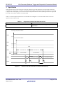
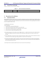
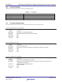
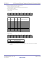
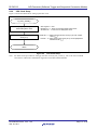
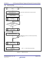
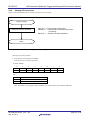
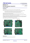
APPLICATION NOTE RL78/G13 A/D Converter (Software Trigger and Sequential Conversion R01AN0452EJ0100 Rev. 1.00 Modes) Sep. 30, 2011 Introduction This application note describes the procedures for performing A/D conversion on analog voltages using the RL78/G13's A/D converter (supporting software trigger and sequential conversion modes). The sample program discussed in this application note performs data conversion on the A/D conversion results and places the converted values in the RL78/G13's internal RAM. Target Device RL78/G13 When applying the sample program covered in this application note to another microcomputer, modify the program according to the specifications for the target microcomputer and conduct an extensive evaluation of the modified program. R01AN0452EJ0100 Rev. 1.00 Sep. 30, 2011 Page 1 of 26 RL78/G13 A/D Converter (Software Trigger and Sequential Conversion Modes) Contents 1. Specification ....................................................................................................................................... 3 2. Operation Check Conditions ................................................................................................................. 4 3. Related Application Note...................................................................................................................... 4 4. 4.1 4.2 Description of the Hardware ................................................................................................................. 5 Hardware Configuration Example ......................................................................................................... 5 List of Pins to be Used ......................................................................................................................... 6 5. Description of the Software .................................................................................................................. 6 5.1 Operation Outline ................................................................................................................................ 6 5.2 List of Option Byte Settings.................................................................................................................. 7 5.3 List of Variables .................................................................................................................................. 7 5.4 List of Functions.................................................................................................................................. 8 5.5 Function Specifications ........................................................................................................................ 8 5.6 Flowcharts .......................................................................................................................................... 9 5.6.1 Initialization Function ................................................................................................................... 10 5.6.2 System function............................................................................................................................ 11 5.6.3 I/O Port Setup .............................................................................................................................. 12 5.6.4 CPU Clock Setup ......................................................................................................................... 14 5.6.5 Setting up the A/D Converter......................................................................................................... 15 5.6.6 Main Processing ........................................................................................................................... 22 5.6.7 Enabling the A/D Voltage Comparator ........................................................................................... 23 5.6.8 Starting A/D Conversion ............................................................................................................... 24 5.6.9 Storing A/D Conversion Results in RAM ....................................................................................... 25 6. Sample Code ..................................................................................................................................... 26 7. Documents for Reference ................................................................................................................... 26 Revision Record ........................................................................................................................................ 27 General Precautions in the Handling of MPU/MCU Products ........................................................................ 28 R01AN0452EJ0100 Rev. 1.00 Sep. 30, 2011 Page 2 of 26 RL78/G13 1. A/D Converter (Software Trigger and Sequential Conversion Modes) Specification This application note provides examples of using the software trigger and sequential conversion modes of the A/D converter. The A/D converter is placed in select mode and the analog signal input from the P20/ANI0 pin is converted to digital values. Subsequently, the conversion result is subjected to data conversion (shifting the data to the right) and the result is stored in the RL78/G13's internal RAM. Table 1.1 lists the Peripheral Function to be Used and its Use and figure 1.1 shows the outline of the conversion operation of the A/D converter. Table 1.1 Peripheral Function to be Used and its Use Peripheral Function A/D converter Use Converts the level of the analog signal input from the P20/ANI0 pin. A/D voltage comparator enabled ADCE A/D conversion enabled ADCS ADS ANI0 Conversion time Status Power down Conversion standby A/D conversion Conversion time A/D conversion Conversion results ADCR Conversion results INTAD Figure 1.1 R01AN0452EJ0100 Rev. 1.00 Sep. 30, 2011 Outline of the A/D Converter Conversion Processing Page 3 of 26 RL78/G13 2. A/D Converter (Software Trigger and Sequential Conversion Modes) Operation Check Conditions The sample code contained in this application note has been checked under the conditions listed in the table below. Table 2.1 Item Microcontroller used Operating frequency Operating voltage Operation Check Conditions Description RL78/G13 (R5F100LEA) High-speed on-chip oscillator (HOCO) clock: 32 MHz CPU/peripheral hardware clock: 32 MHz 5.0 V (can run on a voltage range of 3.9 V to 5.5 V.) LVD operation (VLVI): Reset mode 3.75 V +/- 0.07 V Integrated development environment CubeSuite + V1.00.01 from Renesas Electronics Corp. C compiler CA78K0R V1.20 from Renesas Electronics Corp. 3. Related Application Note The application note that is related to this application note is listed below for reference. RL78/G13 Initialization (R01AN0451EJ0100) Application Note R01AN0452EJ0100 Rev. 1.00 Sep. 30, 2011 Page 4 of 26 RL78/G13 4. 4.1 A/D Converter (Software Trigger and Sequential Conversion Modes) Description of the Hardware Hardware Configuration Example Figure 4.1 shows an example of hardware configuration that is used for this application note. VDD VDD EVDD RESET VDD RL78/G13 REGC EVSS VSS Figure 4.1 P20/ANI0 Target analog input signal P40/TOOL0 For on-chip debugger Hardware Configuration Notes: 1. The purpose of this circuit is only to provide the connection outline and the circuit is simplified accordingly. When designing and implementing an actual circuit, provide proper pin treatment and make sure that the hardware's electrical specifications are met (connect the input-dedicated ports separately to VDD or VSS via a resistor). 2. Connect any pins whose name begins with EVSS to VSS and any pins whose name begins with EVDD to VDD, respectively. 3. VDD must be held at not lower than the reset release voltage (VLVI) that is specified as LVD. R01AN0452EJ0100 Rev. 1.00 Sep. 30, 2011 Page 5 of 26 RL78/G13 4.2 A/D Converter (Software Trigger and Sequential Conversion Modes) List of Pins to be Used Table 4.1 lists the Pin to be Used and its Function. Table 4.1 Pin Name P20/ANI0 5. 5.1 I/O Input Pin to be Used and its Function Description A/D converter analog input port Description of the Software Operation Outline This sample code performs A/D conversion on the analog voltage that is input to pin ANI0 using the software trigger and sequential conversion modes of the A/D converter. It awaits the end of A/D conversion in HALT mode. After A/D conversion is completed, the sample code shifts the result of A/D conversion 6 bits to the right and places the result in the internal RAM of the RL78/G13. (1) Initialize the A/D converter. <Setup conditions> Pin P20/ANI0 is used for the analog input. A/D conversion channel selection mode is set to select mode. A/D conversion operation mode is set to sequential conversion mode. A/D conversion is started using the software trigger. The A/D conversion end interrupt (INTAD) is used. (2) The sample program sets the ADCS bit of the ADM0 register to 1 (A/D conversion start) to start A/D conversion and executes the HALT instruction to place the chip in the HALT mode and wait for an A/D conversion end interrupt. (3) After completing the A/D conversion of the voltage input from pin ANI0, the A/D converter transfers the result of A/D conversion to the ADCR register and generates an A/D conversion end interrupt. (4) On release from the HALT mode in response to the A/D conversion end interrupt, the sample program reads the result of A/D conversion from the ADCR register, shifts the result 6 bits to the right, and stores the shifted data in the internal RAM of the RL78/G13. (5) The chip returns to the HALT mode and waits for an A/D conversion end interrupt. R01AN0452EJ0100 Rev. 1.00 Sep. 30, 2011 Page 6 of 26 RL78/G13 5.2 A/D Converter (Software Trigger and Sequential Conversion Modes) List of Option Byte Settings Table 5.1 summarizes the settings of the option bytes. Table 5.1 Address 000C0H/010C0H Value 01101110B 000C1H/010C1H 000C2H/010C2H 000C3H/010C3H 01010011B 11101000B 10000100B 5.3 Option Byte Settings Description Disables the watchdog timer. (Stops counting after the release of the reset state.) LVD reset mode, 3.75 V +/- 0.07 V HS mode HOCO: 32 MHz Enables the on-chip debugger. List of Variables Table 5.2 lists the global variable that is used by this sample program. Table 5.2 Type unsigned short Variable Name result_buffer R01AN0452EJ0100 Rev. 1.00 Sep. 30, 2011 Global Variable Contents Area for storing the A/D conversion results Function Used main () Page 7 of 26 RL78/G13 5.4 A/D Converter (Software Trigger and Sequential Conversion Modes) List of Functions Table 5.3 lists the functions that are used by this sample program. Table 5.3 Function Name R_ADC_Set_OperationOn R_ADC_Start R_ADC_Get_Result 5.5 Functions Outline Enables the A/D voltage comparator. Starts A/D conversion. Gets A/D conversion results. Function Specifications This section describes the specifications for the functions that are used in the sample code. [Function Name] R_ADC_Set_OperationOn Synopsis Header Declaration Explanation Arguments Return value Remarks Enable A/D voltage comparator. r_cg_adc.h void R_ADC_Set_OperationOn (void) Enables the A/D voltage comparator for operation. None None None [Function Name] R_ADC_Start Synopsis Header Declaration Explanation Arguments Return value Remarks Start A/D conversion. r_cg_adc.h void R_ADC_Start (void) Enables A/D conversion end interrupts and starts A/D conversion processing. None None None [Function Name] R_ADC_Get_Result Synopsis Header Declaration Explanation Arguments Return value Remarks Get A/D conversion results. r_cg_adc.h void R_ADC_Get_Result (uint16_t *buffer) Shifts the A/D conversion results 6 bits to the right and stores the results in the area designated by the argument. Address of the area for storing the A/D conversion results None None R01AN0452EJ0100 Rev. 1.00 Sep. 30, 2011 Page 8 of 26 RL78/G13 5.6 A/D Converter (Software Trigger and Sequential Conversion Modes) Flowcharts Figure 5.1 shows the overall flow of the sample program described in this application note. Start The option bytes are referenced before the initialization function is called. Initialization function hdwinit() main () End Figure 5.1 R01AN0452EJ0100 Rev. 1.00 Sep. 30, 2011 Overall Flow Page 9 of 26 RL78/G13 5.6.1 A/D Converter (Software Trigger and Sequential Conversion Modes) Initialization Function Figure 5.2 shows the flowchart for the initialization function. hdwinit() Disable interrupts IE 0 System function r_systeminit() Enable interrupts IE 1 return Figure 5.2 R01AN0452EJ0100 Rev. 1.00 Sep. 30, 2011 Initialization Function Page 10 of 26 RL78/G13 5.6.2 A/D Converter (Software Trigger and Sequential Conversion Modes) System function Figure 5.3 shows the flowchart for the system function. r_systeminit() Disuse peripheral I/O redirection function PIOR register 00000000B Set up I/O ports PORT_Create() Set up CPU clock R_CGC_Create() Set up A/D converter R_ADC_Create() return Figure 5.3 R01AN0452EJ0100 Rev. 1.00 Sep. 30, 2011 System Function Page 11 of 26 RL78/G13 5.6.3 A/D Converter (Software Trigger and Sequential Conversion Modes) I/O Port Setup Figure 5.4 shows the flowchart for I/O port setup. PORT_Create() Assign P20/ANI0 to analog input (A) ADPC register 02H PM2 register 01H return Figure 5.4 I/O Port Setup Note: Refer to the section entitled "Flowcharts" in RL78/G13 Initialization Application Note (R01AN0451EJ0100) for the configuration of the unused ports. Note: Provide proper treatment for unused pins so that their electrical specifications are observed. Connect each of any unused input-only ports to VDD or VSS via separate resistors. R01AN0452EJ0100 Rev. 1.00 Sep. 30, 2011 Page 12 of 26 RL78/G13 A/D Converter (Software Trigger and Sequential Conversion Modes) Setting up the channel to be used for A/D conversion A/D port configuration register (ADPC) Switches between A/D converter analog input and port digital I/O. Port mode register 2 (PM2) Selects the I/O mode of each port. Symbol: ADPC 7 6 5 4 3 2 1 0 0 0 0 0 ADPC3 ADPC2 ADPC1 ADPC0 0 0 0 0 0 0 1 0 Bits 3 to 0 ADPC3 ADPC2 ADPC1 ADPC0 Available Analog Input 0 0 0 0 ANI0 to ANI14 0 0 0 1 None 0 0 1 0 ANI0 0 0 1 1 ANI0 and ANI1 0 0 0 0 ANI0 to ANI2 0 0 0 1 ANI0 to ANI3 0 0 1 0 ANI0 to ANI4 0 0 1 1 ANI0 to ANI5 0 1 0 0 ANI0 to ANI6 0 1 0 1 ANI0 to ANI7 Other than above Setting prohibited Symbol: PM2 7 6 5 4 3 2 1 0 PM27 PM26 PM25 PM24 PM23 PM22 PM21 PM20 x x x x x x x 1 Bit 0 PM20 PM20 I/O Mode Select 0 Output mode (output buffer on) 1 Input mode (output buffer off) Note: For details on the procedure for setting up the registers, refer to RL78/G13 User's Manual: Hardware. R01AN0452EJ0100 Rev. 1.00 Sep. 30, 2011 Page 13 of 26 RL78/G13 5.6.4 A/D Converter (Software Trigger and Sequential Conversion Modes) CPU Clock Setup Figure 5.5 shows the flowchart for setting up the CPU clock. R_CGC_Create() Set up high-speed system clock/subsystem clock Select CPU/peripheral hardware clock (fCLK) CMC register 00H MSTOP bit 1: Does not use high-speed system clock. XTSTOP bit 1: Does not use subsystem clock. MCM0 bit 0: Select high-speed OCO clock (fIH) as main system clock (fMAIN). CSS bit 0: Select main system clock (fMAIN) as CPU/peripheral hardware clock (fCLK). return Figure 5.5 CPU Clock Setup Note: For details on the procedure for setting up the CPU clock (R_CGC_Create ()), refer to the section entitled "Flowcharts" in RL78/G13 Initialization Application Note (R01AN0451EJ0100). R01AN0452EJ0100 Rev. 1.00 Sep. 30, 2011 Page 14 of 26 RL78/G13 5.6.5 A/D Converter (Software Trigger and Sequential Conversion Modes) Setting up the A/D Converter Figure 5.6 shows the flowchart for setting up the A/D converter. R_ADC_Create() Supply clock to A/D converter circuit Stop A/D converter Clear A/D conversion end interrupt request flag Disable A/D conversion end interrupts Set A/D converter interrupt priority level to 3 Initialize A/D converter Set conversion time to 3 us Select select mode Select software trigger mode Set up reference voltage source 10-bit resolution Set + side reference voltage source to VDD Set - side reference voltage source to VSS Set up upper/lower limit of conversion result comparison Set upper limit comparison to FFH Set lower limit comparison to 00H Specify analog input channel Set analog input channel to ANI0 ADCEN bit 1: Start supply of input clock. ADM0 register 00H ADIF bit 0: Clear interrupt request flag. ADMK bit 1: Disable A/D conversion end interrupts. ADPR0 bit 1 ADPR1 bit 1 ADM0 register 28H Bits FR2 to FR0 = 101B: fCLK/5 (fCLK = 32 MHz) ADMD bit 0: Select mode ADM1 register 00H Bits ADTMD1 and ADTMD0 = 00B : Software trigger mode ADM2 register FFH ADTYP 0: 10-bit resolution Bits ADREFP1 and ADREF0 = 00B : Supply power from VDD ADREFM 0: Supply power from VSS ADUL register FFH Sets the upper limit of conversion result comparison. ADLL register 00H Sets the lower limit of conversion result comparison. ADS register 00H Bits ADS4 to ADS0 = 00000B ADISS bit 0 return Figure 5.6 R01AN0452EJ0100 Rev. 1.00 Sep. 30, 2011 A/D Converter Setup Flowchart Page 15 of 26 RL78/G13 A/D Converter (Software Trigger and Sequential Conversion Modes) Starting the supply of clock to the A/D converter Peripheral enable register 0 (PER0) Starts the supply of the clock to the A/D converter. Symbol: PER0 7 6 5 4 3 2 1 0 RTCEN IICA1EN ADCEN IICA0EN SAU1EN SAU0EN TAU1EN TAU0EN x 0 1 x x x 0 x Bit 5 ADCEN 0 1 A/D converter input clock control Stops supply of input clock. Starts supply of input clock. Note: For details on the register setup procedures, refer to RL78/G13 User's Manual: Hardware. R01AN0452EJ0100 Rev. 1.00 Sep. 30, 2011 Page 16 of 26 RL78/G13 A/D Converter (Software Trigger and Sequential Conversion Modes) Setting up the A/D conversion time and operation mode A/D converter mode register 0 (ADM0) Controls the A/D conversion operation. Specifies the A/D conversion channel selection mode. Symbol: ADM0 7 6 5 4 3 2 1 0 ADCS ADMD FR2 FR1 FR0 LV1 LV0 ADCE x 0 1 0 1 0 0 x Bit 6 ADMD 0 1 A/D channel selection mode select Select mode Scan mode Bits 5 to 1 ADM0 Mode FR2 FR1 FR0 LV1 LV0 0 0 Conversion Time Selection fCLK = 1 MHz fCLK = 4 MHz fCLK = 8 MHz fCLK = 16 MHz fCLK = 32 MHz Conversion Clock (fAD) 38 s fCLK/64 0 0 0 0 0 1 0 1 0 0 1 1 38 s 1 0 0 28.5 s 14.25 s 7.125 s 3.5625 s fCLK/6 1 0 1 23.75 s 11.875 s 5.938 s 2.9688 s fCLK/5 1 1 0 1 1 1 0 0 0 0 0 1 0 1 0 0 1 1 1 0 0 25.5 s 12.75 s 6.375 s 3.1875 s fCLK/6 1 0 1 21.25 s 10.625 s 5.3125 s 2.6536 s fCLK/5 1 1 0 1 1 1 x x x 1 0 Low voltage 1 Setting prohibited x x x 1 1 Low voltage 2 Setting prohibited Standard Setting Setting Setting Setting 1 prohibited prohibited prohibited prohibited 38 s 0 1 Standard 2 38 s 19 s fCLK/32 38 s 19 s 9.5 s fCLK/16 19 s 9.5 s 4.75 s fCLK/8 19 s 9.5 s 4.75 s 2.375 s fCLK/4 9.5 s 4.75 s 2.375 s Setting prohibited fCLK/2 34 s fCLK/64 Setting Setting Setting Setting prohibited prohibited prohibited prohibited 34 s 34 s 34 s 17 s fCLK/32 34 s 17 s 8.5 s fCLK/16 17 s 8.5 s 4.25 s fCLK/8 17 s 8.5 s 4.25 s 2.125 s fCLK/4 8.5 s 4.25 s 2.125 s Setting prohibited fCLK/2 Note: For details on the register setup procedures, refer to RL78/G13 User's Manual: Hardware. R01AN0452EJ0100 Rev. 1.00 Sep. 30, 2011 Page 17 of 26 RL78/G13 A/D Converter (Software Trigger and Sequential Conversion Modes) Setting up the A/D conversion trigger mode A/D converter mode register 1 (ADM1) Selects the A/D conversion trigger mode. Selects the A/D conversion mode. Symbol: ADM1 7 6 5 ADTMD1 ADTMD0 ADSCM 0 0 0 4 3 2 0 0 0 0 0 0 1 0 ADTRS1 ADTRS0 0 0 Bits 1 and 0 ADTRS1 ADTRS0 Selection of the hardware trigger signal 0 0 Do not use the hardware trigger. 0 1 End of timer channel 1 count or capture end interrupt signal (INTTM01) 1 1 0 1 Real-time clock interrupt signal (INTRTC) Interval timer interrupt signal (INTIT) Bit 5 ADSCM Specification of the A/D conversion mode 0 1 Sequential conversion mode One-shot conversion mode Bits 7 and 6 ADTMD1 ADTMD0 Selection of the A/D conversion trigger mode 0 Software trigger mode 1 1 0 1 Hardware trigger no-wait mode Hardware trigger wait mode Note: For details on the register setup procedures, refer to RL78/G13 User's Manual: Hardware. R01AN0452EJ0100 Rev. 1.00 Sep. 30, 2011 Page 18 of 26 RL78/G13 A/D Converter (Software Trigger and Sequential Conversion Modes) Setting up the reference voltage A/D converter mode register 2 (ADM2) Sets up the reference voltage source. Symbol: ADM2 7 6 5 ADREFP1 ADREFP0 ADREFM 0 0 0 4 3 2 1 0 0 ADCRK AWC 0 ADTYP 0 0 0 0 0 Bit 0 ADTYP 0 1 Selection of the A/D conversion resolution 10-bit resolution 8-bit resolution Bit 2 AWC 0 1 Specification of the wakeup function (SNOOZE mode) Do not use the SNOOZE mode function. Use the SNOOZE mode function. Bit 3 Checking the upper limit and lower limit conversion result values ADCRK 0 1 The interrupt signal (INTAD) is output when the ADLL register the ADCR register the ADUL register. Interrupt signal (INTAD) is output when ADCR register < ADLL register and ADUL register < ADCR register. Bit 5 Selection of the side reference voltage source of the A/D converter ADREFM 0 1 Supplied from VSS. Supplied from P21/AVREFM/ANI1. Bits 7 and 6 ADREFP1 ADREFP0 Selection of the side reference voltage source of the A/D converter 0 0 Supplied from VDD. 0 1 Supplied from P20/AVREFP/ANI0. 1 1 0 1 Supplied from internal reference voltage (1.44 V). Setting prohibited Note: For details on the register setup procedures, refer to RL78/G13 User's Manual: Hardware. R01AN0452EJ0100 Rev. 1.00 Sep. 30, 2011 Page 19 of 26 RL78/G13 A/D Converter (Software Trigger and Sequential Conversion Modes) Setting up the conversion result comparison upper limit/lower limit Conversion result comparison upper limit setting register (ADUL) Conversion result comparison lower limit setting register (ADLL) Sets up the conversion result comparison upper- and lower-limit values. Symbol: ADUL 7 6 5 4 3 2 1 0 ADUL7 ADUL6 ADUL5 ADUL4 ADUL3 ADUL2 ADUL1 ADUL0 1 1 1 1 1 1 1 1 Symbol: ADLL 7 6 5 4 3 2 1 0 ADLL7 ADLL6 ADLL5 ADLL4 ADLL3 ADLL2 ADLL1 ADLL0 0 0 0 0 0 0 0 0 Specifying the input channel Analog input channel specification register (ADS) Specifies the input channel for the analog voltage to be subjected to A/D conversion. Symbol: ADS 7 6 5 4 3 2 1 0 ADISS 0 0 ADS4 ADS3 ADS2 ADS1 ADS0 0 0 0 0 0 0 0 0 ADIS S ADS4 ADS3 ADS2 ADS1 ADS0 0 0 0 0 0 0 ANI0 P20/ANI0 pin/AVREFP pin 0 0 0 0 0 1 ANI1 P21/ANI1 pin/AVREFM pin 0 0 0 0 1 0 ANI2 P22/ANI2 pin 0 0 0 0 1 1 ANI3 P23/ANI3 pin 0 0 0 1 0 0 ANI4 P24/ANI4 pin 0 0 0 1 0 1 ANI5 P25/ANI5 pin 0 0 0 1 1 0 ANI6 P26/ANI6 pin 0 0 0 1 1 1 ANI7 P27/ANI7 pin 0 1 0 0 0 0 ANI16 P03/ANI16 pin 0 1 0 0 0 1 ANI17 P02/ANI17 pin 0 1 0 0 1 0 ANI18 P147/ANI18 pin Bits 7, 4 to 0 Analog Input Channel Input Source 0 1 0 0 1 1 ANI19 P120/ANI19 pin 1 0 0 0 0 0 Temperature sensor 0 output 1 0 0 0 0 1 Internal reference voltage output (1.44 V) Other than above Setting prohibited Note: For details on the register setup procedures, refer to RL78/G13 User's Manual: Hardware. R01AN0452EJ0100 Rev. 1.00 Sep. 30, 2011 Page 20 of 26 RL78/G13 A/D Converter (Software Trigger and Sequential Conversion Modes) Setting up end of A/D conversion interrupts Interrupt request flag register (IF1H) Clears the interrupt request flag. Interrupt mask flag register (MK1H) Disables interrupts. Symbol: IF1H 7 TMIF04 x 6 5 4 SRIF3 STIF3 TMIF13 CSIIF31 CSIIF30 IICIF31 IICIF30 x x 3 2 1 0 KRIF ITIIF RTCIF ADIF x x x 0 x Bit 0 ADIF Interrupt request flag 0 No interrupt request signal is generated. 1 Interrupt request is generated, interrupt request status Symbol: MK1H 7 6 5 4 SRMK3 STMK3 TMMK04 TMMK13 CSIMK31 CSIMK30 IICMK31 IICMK30 x x x 3 2 1 0 KRMK ITIMK RTCMK ADMK x x x 1 x Bit 0 ADMK 0 1 Interrupt processing control Enables interrupt processing. Disables interrupt processing. Note: For details on the register setup procedures, refer to RL78/G13 User's Manual: Hardware. R01AN0452EJ0100 Rev. 1.00 Sep. 30, 2011 Page 21 of 26 RL78/G13 5.6.6 A/D Converter (Software Trigger and Sequential Conversion Modes) Main Processing Figure 5.7 shows the flowchart for the main processing routine. main() Variable: Initialize result_buffer to 00h result_buffer: Holds the A/D conversion results. IE 0 Disable interrupts Enable A/D voltage comparator R_ADC_Set_OperationOn() A/D voltage comparator stabilization time elapsed? No Yes Start A/D conversion R_ADC_Start() Switch into HALT mode Set A/D conversion end interrupt request flag. ADIF 1 Store A/D conversion results in RAM R_ADC_Get_Result() Clear A/D conversion end interrupt request flag Figure 5.7 R01AN0452EJ0100 Rev. 1.00 Sep. 30, 2011 ADIF 0: Clear interrupt request flag. Main Processing Page 22 of 26 RL78/G13 5.6.7 A/D Converter (Software Trigger and Sequential Conversion Modes) Enabling the A/D Voltage Comparator Figure 5.8 shows the flowchart for enabling the A/D voltage comparator. R_ADC_Set_OperationOn() Enable A/D voltage comparator ADCE bit 1 return Figure 5.8 Enabling the A/D Voltage Comparator Starting the A/D voltage comparator A/D converter mode register 0 (ADM0) Controls the operation of the A/D voltage comparator. Symbol: ADM0 7 6 5 4 3 2 1 0 ADCS ADMD FR2 FR1 FR0 LV1 LV0 ADCE x x x x x x x 1 Bit 0 ADCE A/D voltage comparator operation control 0 Stops A/D voltage comparator operation. 1 Enables A/D voltage comparator operation. Note: For details on the register setup procedures, refer to RL78/G13 User's Manual: Hardware. R01AN0452EJ0100 Rev. 1.00 Sep. 30, 2011 Page 23 of 26 RL78/G13 5.6.8 A/D Converter (Software Trigger and Sequential Conversion Modes) Starting A/D Conversion Figure 5.9 shows the flowchart for starting A/D conversion processing. R_ADC_Start() ADIF bit 0: Clear interrupt request flag. ADMK bit 1: Disable A/D conversion end interrupt processing. ADCS bit =: Enable conversion operation. Start A/D converter operation return Figure 5.9 Starting A/D Conversion Starting conversion operation A/D converter mode register 0 (ADM0) Controls the A/D conversion operation. Symbol: ADM0 7 6 5 4 3 2 1 0 ADCS ADMD FR2 FR1 FR0 LV1 LV2 ADCE 1 x x x x x x 1 Bit 7 ADCS A/D conversion operation control 0 Stops conversion operation. 1 Enables conversion operation. Note: For details on the register setup procedures, refer to RL78/G13 User's Manual: Hardware. R01AN0452EJ0100 Rev. 1.00 Sep. 30, 2011 Page 24 of 26 RL78/G13 5.6.9 A/D Converter (Software Trigger and Sequential Conversion Modes) Storing A/D Conversion Results in RAM Figure 5.10 shows the flowchart for storing the A/D conversion results in RAM. R_ADC_Get_Result() Shift A/D conversion results 6 bits to right Store shifted value in variable result_buffer = (ADCR >> 6) ADCR: 10-bit A/D conversion result register result_buffer: Variable in RAM return Figure 5.10 R01AN0452EJ0100 Rev. 1.00 Sep. 30, 2011 Storing the A/D Conversion Results in RAM Page 25 of 26 RL78/G13 6. A/D Converter (Software Trigger and Sequential Conversion Modes) Sample Code The sample code is available on the Renesas Electronics Website. 7. Documents for Reference RL78/G13 User's Manual: Hardware Rev.0.07 (R01UH0146EJ0007) RL78 Family User's Manual: Software Rev.1.00 (R01US0015EJ0100) (The latest versions of the documents are available on the Renesas Electronics Website.) Technical Updates/Technical Brochures (The latest versions of the documents are available on the Renesas Electronics Website.) Website and Support Renesas Electronics Website http://www.renesas.com/index.jsp Inquiries http://www.renesas.com/contact/ R01AN0452EJ0100 Rev. 1.00 Sep. 30, 2011 Page 26 of 26 Revision Record Rev. Date 1.00 Sep. 30, 2011 RL78/G13 A/D Converter (Software Trigger and Sequential Conversion Modes) Page — Description Summary First edition issued All trademarks and registered trademarks are the property of their respective owners. A-1 General Precautions in the Handling of MPU/MCU Products The following usage notes are applicable to all MPU/MCU products from Renesas. For detailed usage notes on the products covered by this manual, refer to the relevant sections of the manual. If the descriptions under General Precautions in the Handling of MPU/MCU Products and in the body of the manual differ from each other, the description in the body of the manual takes precedence. 1. Handling of Unused Pins Handle unused pins in accord with the directions given under Handling of Unused Pins in the manual. The input pins of CMOS products are generally in the high-impedance state. In operation with unused pin in the open-circuit state, extra electromagnetic noise is induced in the vicinity of LSI, an associated shoot-through current flows internally, and malfunctions occur due to the false recognition of the pin state as an input signal become possible. Unused pins should be handled as described under Handling of Unused Pins in the manual. 2. Processing at Power-on The state of the product is undefined at the moment when power is supplied. The states of internal circuits in the LSI are indeterminate and the states of register settings and pins are undefined at the moment when power is supplied. In a finished product where the reset signal is applied to the external reset pin, the states of pins are not guaranteed from the moment when power is supplied until the reset process is completed. In a similar way, the states of pins in a product that is reset by an on-chip power-on reset function are not guaranteed from the moment when power is supplied until the power reaches the level at which resetting has been specified. 3. Prohibition of Access to Reserved Addresses Access to reserved addresses is prohibited. The reserved addresses are provided for the possible future expansion of functions. Do not access these addresses; the correct operation of LSI is not guaranteed if they are accessed. 4. Clock Signals After applying a reset, only release the reset line after the operating clock signal has become stable. When switching the clock signal during program execution, wait until the target clock signal has stabilized. When the clock signal is generated with an external resonator (or from an external oscillator) during a reset, ensure that the reset line is only released after full stabilization of the clock signal. Moreover, when switching to a clock signal produced with an external resonator (or by an external oscillator) while program execution is in progress, wait until the target clock signal is stable. 5. Differences between Products Before changing from one product to another, i.e. to one with a different part number, confirm that the change will not lead to problems. The characteristics of MPU/MCU in the same group but having different part numbers may differ because of the differences in internal memory capacity and layout pattern. When changing to products of different part numbers, implement a system-evaluation test for each of the products. Notice 1. All information included in this document is current as of the date this document is issued. Such information, however, is subject to change without any prior notice. Before purchasing or using any Renesas Electronics products listed herein, please confirm the latest product information with a Renesas Electronics sales office. Also, please pay regular and careful attention to additional and different information to be disclosed by Renesas Electronics such as that disclosed through our website. 2. Renesas Electronics does not assume any liability for infringement of patents, copyrights, or other intellectual property rights of third parties by or arising from the use of Renesas Electronics products or technical information described in this document. No license, express, implied or otherwise, is granted hereby under any patents, copyrights or other intellectual property rights of Renesas Electronics or others. 3. You should not alter, modify, copy, or otherwise misappropriate any Renesas Electronics product, whether in whole or in part. 4. Descriptions of circuits, software and other related information in this document are provided only to illustrate the operation of semiconductor products and application examples. You are fully responsible for the incorporation of these circuits, software, and information in the design of your equipment. Renesas Electronics assumes no responsibility for any losses incurred by you or third parties arising from the use of these circuits, software, or information. 5. When exporting the products or technology described in this document, you should comply with the applicable export control laws and regulations and follow the procedures required by such laws and regulations. You should not use Renesas Electronics products or the technology described in this document for any purpose relating to military applications or use by the military, including but not limited to the development of weapons of mass destruction. Renesas Electronics products and technology may not be used for or incorporated into any products or systems whose manufacture, use, or sale is prohibited under any applicable domestic or foreign laws or regulations. 6. Renesas Electronics has used reasonable care in preparing the information included in this document, but Renesas Electronics does not warrant that such information is error free. Renesas Electronics 7. Renesas Electronics products are classified according to the following three quality grades: "Standard", "High Quality", and "Specific". The recommended applications for each Renesas Electronics product assumes no liability whatsoever for any damages incurred by you resulting from errors in or omissions from the information included herein. depends on the product's quality grade, as indicated below. You must check the quality grade of each Renesas Electronics product before using it in a particular application. You may not use any Renesas Electronics product for any application categorized as "Specific" without the prior written consent of Renesas Electronics. Further, you may not use any Renesas Electronics product for any application for which it is not intended without the prior written consent of Renesas Electronics. Renesas Electronics shall not be in any way liable for any damages or losses incurred by you or third parties arising from the use of any Renesas Electronics product for an application categorized as "Specific" or for which the product is not intended where you have failed to obtain the prior written consent of Renesas Electronics. The quality grade of each Renesas Electronics product is "Standard" unless otherwise expressly specified in a Renesas Electronics data sheets or data books, etc. "Standard": Computers; office equipment; communications equipment; test and measurement equipment; audio and visual equipment; home electronic appliances; machine tools; personal electronic equipment; and industrial robots. "High Quality": Transportation equipment (automobiles, trains, ships, etc.); traffic control systems; anti-disaster systems; anti-crime systems; safety equipment; and medical equipment not specifically designed for life support. "Specific": Aircraft; aerospace equipment; submersible repeaters; nuclear reactor control systems; medical equipment or systems for life support (e.g. artificial life support devices or systems), surgical implantations, or healthcare intervention (e.g. excision, etc.), and any other applications or purposes that pose a direct threat to human life. 8. You should use the Renesas Electronics products described in this document within the range specified by Renesas Electronics, especially with respect to the maximum rating, operating supply voltage range, movement power voltage range, heat radiation characteristics, installation and other product characteristics. Renesas Electronics shall have no liability for malfunctions or damages arising out of the use of Renesas Electronics products beyond such specified ranges. 9. Although Renesas Electronics endeavors to improve the quality and reliability of its products, semiconductor products have specific characteristics such as the occurrence of failure at a certain rate and malfunctions under certain use conditions. Further, Renesas Electronics products are not subject to radiation resistance design. Please be sure to implement safety measures to guard them against the possibility of physical injury, and injury or damage caused by fire in the event of the failure of a Renesas Electronics product, such as safety design for hardware and software including but not limited to redundancy, fire control and malfunction prevention, appropriate treatment for aging degradation or any other appropriate measures. Because the evaluation of microcomputer software alone is very difficult, please evaluate the safety of the final products or system manufactured by you. 10. Please contact a Renesas Electronics sales office for details as to environmental matters such as the environmental compatibility of each Renesas Electronics product. Please use Renesas Electronics products in compliance with all applicable laws and regulations that regulate the inclusion or use of controlled substances, including without limitation, the EU RoHS Directive. Renesas Electronics assumes no liability for damages or losses occurring as a result of your noncompliance with applicable laws and regulations. 11. This document may not be reproduced or duplicated, in any form, in whole or in part, without prior written consent of Renesas Electronics. 12. Please contact a Renesas Electronics sales office if you have any questions regarding the information contained in this document or Renesas Electronics products, or if you have any other inquiries. (Note 1) "Renesas Electronics" as used in this document means Renesas Electronics Corporation and also includes its majority-owned subsidiaries. (Note 2) "Renesas Electronics product(s)" means any product developed or manufactured by or for Renesas Electronics. http://www.renesas.com SALES OFFICES Refer to "http://www.renesas.com/" for the latest and detailed information. Renesas Electronics America Inc. 2880 Scott Boulevard Santa Clara, CA 95050-2554, U.S.A. Tel: +1-408-588-6000, Fax: +1-408-588-6130 Renesas Electronics Canada Limited 1101 Nicholson Road, Newmarket, Ontario L3Y 9C3, Canada Tel: +1-905-898-5441, Fax: +1-905-898-3220 Renesas Electronics Europe Limited Dukes Meadow, Millboard Road, Bourne End, Buckinghamshire, SL8 5FH, U.K Tel: +44-1628-585-100, Fax: +44-1628-585-900 Renesas Electronics Europe GmbH Arcadiastrasse 10, 40472 Düsseldorf, Germany Tel: +49-211-65030, Fax: +49-211-6503-1327 Renesas Electronics (China) Co., Ltd. 7th Floor, Quantum Plaza, No.27 ZhiChunLu Haidian District, Beijing 100083, P.R.China Tel: +86-10-8235-1155, Fax: +86-10-8235-7679 Renesas Electronics (Shanghai) Co., Ltd. Unit 204, 205, AZIA Center, No.1233 Lujiazui Ring Rd., Pudong District, Shanghai 200120, China Tel: +86-21-5877-1818, Fax: +86-21-6887-7858 / -7898 Renesas Electronics Hong Kong Limited Unit 1601-1613, 16/F., Tower 2, Grand Century Place, 193 Prince Edward Road West, Mongkok, Kowloon, Hong Kong Tel: +852-2886-9318, Fax: +852 2886-9022/9044 Renesas Electronics Taiwan Co., Ltd. 13F, No. 363, Fu Shing North Road, Taipei, Taiwan Tel: +886-2-8175-9600, Fax: +886 2-8175-9670 Renesas Electronics Singapore Pte. Ltd. 1 harbourFront Avenue, #06-10, keppel Bay Tower, Singapore 098632 Tel: +65-6213-0200, Fax: +65-6278-8001 Renesas Electronics Malaysia Sdn.Bhd. Unit 906, Block B, Menara Amcorp, Amcorp Trade Centre, No. 18, Jln Persiaran Barat, 46050 Petaling Jaya, Selangor Darul Ehsan, Malaysia Tel: +60-3-7955-9390, Fax: +60-3-7955-9510 Renesas Electronics Korea Co., Ltd. 11F., Samik Lavied' or Bldg., 720-2 Yeoksam-Dong, Kangnam-Ku, Seoul 135-080, Korea Tel: +82-2-558-3737, Fax: +82-2-558-5141 © 2011 Renesas Electronics Corporation. All rights reserved. Colophon 1.1