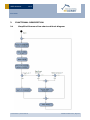
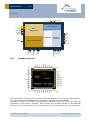
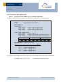
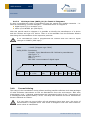
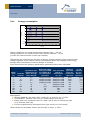
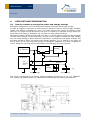
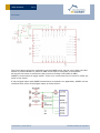
1
USER MANUAL V0.6 Scavenger Transceiver Module STM 400J 13 May 2013 Observe precautions! Electrostatic sensitive devices! Patent protected: WO98/36395, DE 100 25 561, DE 101 50 128, WO 2004/051591, DE 103 01 678 A1, DE 10309334, WO 04/109236, WO 05/096482, WO 02/095707, US 6,747,573, US 7,019,241 EnOcean GmbH Kolpingring 18a 82041 Oberhaching Germany Phone +49.89.67 34 689-0 Fax +49.89.67 34 689-50 [email protected] www.enocean.com Subject to modifications STM 400J User Manual V0.6 May 13, 2013 Page 1/38 USER MANUAL V0.6 STM 400J REVISION HISTORY The following major modifications and improvements have been made to the first version of this document: No 0.5 0.6 Major Changes Initial version Update with more data Published by EnOcean GmbH, Kolpingring 18a, 82041 Oberhaching, Germany www.enocean.com, [email protected], phone +49 (89) 6734 6890 © EnOcean GmbH All Rights Reserved Important! This information describes the type of component and shall not be considered as assured characteristics. No responsibility is assumed for possible omissions or inaccuracies. Circuitry and specifications are subject to change without notice. For the latest product specifications, refer to the EnOcean website: http://www.enocean.com. As far as patents or other rights of third parties are concerned, liability is only assumed for modules, not for the described applications, processes and circuits. EnOcean does not assume responsibility for use of modules described and limits its liability to the replacement of modules determined to be defective due to workmanship. Devices or systems containing RF components must meet the essential requirements of the local legal authorities. The modules must not be used in any relation with equipment that supports, directly or indirectly, human health or life or with applications that can result in danger for people, animals or real value. Components of the modules are considered and should be disposed of as hazardous waste. Local government regulations are to be observed. Packing: Please use the recycling operators known to you. © 2013 EnOcean | www.enocean.com STM 400J User Manual V0.6 | Page 2/38 USER MANUAL V0.6 STM 400J TABLE OF CONTENT 1 2 MODULE VARIANTS AND RELATED DOCUMENTS................................................ 4 GENERAL DESCRIPTION ................................................................................. 4 Basic functionality ......................................................................................... 4 Technical data ............................................................................................... 5 Physical dimensions ....................................................................................... 5 Environmental conditions................................................................................ 6 Ordering Information ..................................................................................... 6 FUNCTIONAL DESCRIPTION ............................................................................ 7 3.1 Simplified firmware flow chart and block diagram .............................................. 7 3.2 Hardware pin out........................................................................................... 8 3.3 Pin description and operational characteristics ................................................... 9 3.3.1 GPIO supply voltage................................................................................. 11 3.3.2 Analog and digital inputs .......................................................................... 12 3.4 Absolute maximum ratings (non operating) .................................................... 13 3.5 Maximum ratings (operating) ........................................................................ 13 3.6 Power management and voltage regulators..................................................... 13 3.7 Charge control output (CCO) ......................................................................... 14 3.8 Configuration .............................................................................................. 15 3.8.1 Configuration via pins .............................................................................. 15 3.8.2 Configuration via programming interface .................................................... 16 3.9 Radio telegram............................................................................................ 17 3.9.1 Normal operation..................................................................................... 17 3.9.2 Teach-in telegram.................................................................................... 21 3.10 Transmit timing ...................................................................................... 21 3.11 Energy consumption ............................................................................... 22 2.1 2.2 2.3 2.4 2.5 3 4 APPLICATIONS INFORMATION....................................................................... 23 4.1 How to connect an energy harvester and energy storage .................................. 23 4.2 Using the SCO pin ....................................................................................... 25 4.3 Using the WAKE pins .................................................................................... 25 4.4 Using RVDD ................................................................................................ 27 4.5 Antenna options STM 400 ............................................................................. 28 4.5.1 Overview ................................................................................................ 28 4.5.2 Whip antenna.......................................................................................... 28 4.5.3 Helical antenna ....................................................................................... 28 4.6 Positioning of the whip antenna ..................................................................... 29 4.7 Recommendations for laying a whip antenna................................................... 30 4.8 Layout recommendations for foot pattern ....................................................... 31 4.9 Soldering information................................................................................... 35 4.10 Tape & Reel specification ......................................................................... 36 4.11 Transmission range................................................................................. 37 5 AGENCY CERTIFICATIONS ............................................................................ 38 5.1 Japanese Type Approval ............................................................................... 38 © 2013 EnOcean | www.enocean.com STM 400J User Manual V0.6 | Page 3/38 USER MANUAL V0.6 STM 400J 1 MODULE VARIANTS AND RELATED DOCUMENTS This document describes operation of STM 400J modules with their built-in firmware. If you want to write own firmware running on the integrated micro controller or need more detailed information on the Dolphin core please also refer to: Dolphin Core Description Dolphin API Documentation In addition we recommend following our application notes, in particular: AN102: Antenna Basics – Basic Antenna Design Considerations for EnOcean based Products AN207: ECS 300/310 Solar Panel - Design Considerations AN208: Energy Storage – Design Considerations AN209: STM 300 THERMO OR BATTERY POWERED – Power Supply Alternatives to Solar Panel 2 2.1 GENERAL DESCRIPTION Basic functionality The extremely power saving RF transmitter module STM 400 of EnOcean enables the realization of wireless and maintenance free sensors and actuators such as room operating panels, motion sensors or valve actuators for heating control. Power supply is provided by an external energy harvester, e.g. a small solar cell (e.g. EnOcean ECS 3x0) or a thermal harvester. An energy storage device can be connected externally to bridge periods with no supply from the energy harvester. A voltage limiter avoids damaging of the module when the supply from the energy harvester gets too high. The module provides a user configurable cyclic wake up. After wake up a radio telegram (input data, unique 32 bit sensor ID, checksum) will be transmitted in case of a change of any digital input value compared to the last sending or in case of a significant change of measured analogue values (different input sensitivities can be selected). In case of no relevant input change a redundant retransmission signal is sent after a user configurable number of wake-ups to announce all current values. In addition a wake up can be tri ggered externally. Features with built-in firmware 3 A/D converter inputs 4 digital inputs Configurable wake-up and transmission cycle © 2013 EnOcean | www.enocean.com STM 400J User Manual V0.6 | Page 4/38 USER MANUAL V0.6 STM 400J Wake-up via Wake pins Voltage limiter Threshold detector Application notes for calculation of energy budgets and management of external energy storages Product variants STM 400J / Features accessible via API Using the Dolphin API library it is possible to write custom firmware for the module. STM 400J is in-system programmable. The API provides: Integrated 16.384MHz 8051 CPU with 64 kB FLASH and 4 kB SRAM Receiver functionality Various power down and sleep modes down to typ. 0.1 µA current consumption Up to 16 configurable I/Os 10 bit ADC, 8 bit DAC 2.2 Technical data Antenna External whip or 50 Ω antenna mountable Frequency Data rate 928.35 MHz (FSK) 125 kbps typ. -95 dBm1 Receiver Sensitivity (at 25 °C) only via API Conducted Output Power @ 50 Ohm Power Supply 0dBm 2.1 V–5 V, 2.6 V needed for start-up Current Consumption Input Channels Deep Sleep mode : typ. 0.1 µA Transmit mode: typ. 16 mA Receive mode (via API only): typ. 22 mA 4x digital input, 2x WAKE input , 3x analog input Resolution: 3x 8 bit or 1x 10 bit, 1x 8 bit, 1x 6 bit Radio Regulations 2.3 Physical dimensions PCB dimensions Weight 1 ARIB STD-T108 22 x 19 x 3.1 mm 1.9 g @ 0.1% telegram error rate (based on transmitted sub-telegrams) © 2013 EnOcean | www.enocean.com STM 400J User Manual V0.6 | Page 5/38 USER MANUAL V0.6 STM 400J Unless otherwise specified dimensions are in mm. Tolerances: PCB outline dimensions 0.2 mm All other tolerances 0.1 mm STM 400J (pads on bottom side of PCB!) 2.4 Environmental conditions Operating temperature -25 °C … +85 °C Storage temperature -40 °C … +85 °C Storage temperature in tape & reel package Humidity 2.5 Type STM 400 -20 °C … +50 °C 0% … 93% r.h., non-condensing Ordering Information Ordering Code S3061-D400 Frequency 928.35 MHz Suited solar cells (for technical details please refer to the ECS3x0 data sheet): Type ECS 300 ECS 310 Ordering Code S3005-D305 S3005-D310 © 2013 EnOcean | www.enocean.com Size 35.0 × 12.8 × 1.1 mm 50.0 × 20.0 × 1.1 mm STM 400J User Manual V0.6 | Page 6/38 USER MANUAL V0.6 STM 400J 3 3.1 FUNCTIONAL DESCRIPTION Simplified firmware flow chart and block diagram © 2013 EnOcean | www.enocean.com STM 400J User Manual V0.6 | Page 7/38 USER MANUAL V0.6 STM 400J RF_50 VDD IOVDD GND VDDLIM RF_WHIP RF Transceiver Power Management V_OUT DVDD µController 3.2 PROG_EN CW_0 CW_1 CP_0 CP_1 SCO CCO RESET Ultra Low Power Unit WAKE0 LRN UVDD Mixed I/O Interface LED DI_0 DI_1 DI_2 DI_3 AD_0 AD_1 AD_2 Hardware pin out The figure above shows the pin out of the STM 400 hardware. The pins are named according to the naming of the EO3100I chip to simplify usage of the DOLPHIN API. The table in section 3.3 shows the translation of hardware pins to a naming that fits the functionality of the built-in firmware. When writing own firmware based on the DOLPHIN API please refer to the Dolphin Core Description and use this manual only for information © 2013 EnOcean | www.enocean.com STM 400J User Manual V0.6 | Page 8/38 USER MANUAL V0.6 STM 400J regarding the module hardware, such as pin out, layout recommendations, charging circuitry, antenna options, and approvals. 3.3 STM 400 Hardware Symbol GND Pin description and operational characteristics Function Characteristics Ground connection Must be connected to GND VDD STM 400 STM 400 pin # Firmware Symbol 1, 5, 7, GND 17, 24, 26, 28, 31 2 VDD Supply voltage RVDD 8 V_OUT RF supply voltage regulator output DVDD 25 DVDD Digital supply voltage regulator output UVDD 32 UVDD Ultra low power supply voltage regulator output VDDLIM 3 VDDLIM IOVDD 23 IOVDD Supply voltage limiter input GPIO supply voltage RESET 27 RESET PROG_EN 18 Reset input Programming I/F PROG_EN Programming I/F ADIO0 9 AD_0 Analog input ADIO1 10 AD_1 Analog input ADIO2 11 AD_2 Analog input 2.1 V – 4.5 V; Start-up voltage: 2.6 V Maximum ripple: see 3.6 1.8 V. Output current: max. 10 mA. See 4.4! Supply for external circuitry, available while not in deep sleep mode. 1.8 V. Output current: max. 5 mA Supply for external circuitry, available while not in deep sleep mode. Not for supply of external circuitry! For use with WAKE pins, see section 4.3. Max. 1 µA output current! Limitation voltage: 4.5 V Maximum shunting current: 50 mA Must be connected to desired interface supply voltage as specified in 3.5, e.g. to DVDD. See also 3.3.1 Active high reset (1.8 V) Connect external 10 kΩ pull-down. HIGH: programming mode active LOW: operating mode Digital input, connect external 10 kΩ pull-down. Input read ~2 ms after wake-up. Resolution 8 bit (default) or 10 bit. See also 3.3.2. Input read ~2 ms after wake-up. Resolution 8 bit (default) or 6 bit. See also 3.3.2. Input read ~2 ms after wake-up. Resolution 8 bit. See also 3.3.2. © 2013 EnOcean | www.enocean.com STM 400J User Manual V0.6 | Page 9/38 USER MANUAL V0.6 STM 400J ADIO3 12 DI_0 Digital input ADIO4 13 DI_1 Digital input ADIO5 14 DI_2 Digital input ADIO6 15 DI_3 Digital input ADIO7 16 LED Transmission indicator LED SCSEDIO0 19 CW_1 SCLKDIO1 20 CW_0 WSDADIO2 21 CP_1 RSDADIO3 22 CP_0 WXIDIO 29 SCO Programming I/F Encoding input for wake-up cycle Programming I/F Encoding input for wake-up cycle Programming I/F Encoding input for retransmission Programming I/F Encoding input for retransmission Programming I/F Sensor control WXODIO 30 CCO Charge control WAKE0 33 WAKE0 Wake input WAKE1 34 LRN LRN input RF_WHIP RF_50 4 6 RF_WHIP RF_50 RF output RF output © 2013 EnOcean | www.enocean.com Input read ~2 ms after wake-up. See also 3.3.2. Input read ~2 ms after wake-up. See also 3.3.2. Input read ~2 ms after wake-up. See also 3.3.2. Input read ~2 ms after wake-up. See also 3.3.2. Max. output current: 2 mA @ IOVDD=3.3 V 0.65 mA @ IOVDD=1.8 V Leave open or connect to GND Leave open or connect to GND Leave open or connect to GND Leave open or connect to GND Digital output, max. current 15 µA HIGH ~x ms before analog inputs are read (x=0…508 ms; default 2 ms.) LOW at wake-up and after reading of analog inputs Polarity can be inverted, delay time can be programmed, see 3.8.2. Max output current 15 µA See 3.7 for description of behaviour. Change of logic state leads to wakeup and transmission of a telegram. See also 4.3. Change of logic state to LOW leads to wake-up and transmission of teach-in telegram if a manufacturer code is programmed. See also 0 and 4.3. Output for whip antenna 50 Ohm output for external antenna STM 400J User Manual V0.6 | Page 10/38 USER MANUAL V0.6 STM 400J 3.3.1 GPIO supply voltage For digital communication with other circuitry (peripherals) the digital I/O configured pins of the mixed signal sensor interface (ADIO0 to ADIO7) and the pins of the programming interface (SCSEDIO0, SCLKDIO1, WSDADIO2, RSDADIO3) may be operated from supply voltages different from DVDD. Therefore an interface supply voltage pin IOVDD is available which can be connected either to DVDD or to an external supply within the tolerated voltage range of IOVDD. Please note that the wristwatch XTAL I/Os WXIDIO and WXODIO are always supplied from UVDD. If DVDD=0 V (e.g. in any sleep mode or if VDD<VOFF) and IOVDD is supplied, there may be unpredictable and varying current from IOVDD caused by internal floating nodes. It must be taken care that the current into IOVDD does not exceed 10 mA while DVDD=0 V. If DVDD=0 V and IOVDD is not supplied, do not apply voltage to any above mentioned pin. This may lead to unpredictable malfunction of the device. For I/O pins configured as analog pins the IOVDD voltage level is not relevant! However it is important to connect IOVDD to a supply voltage as specified in 3.5. IOVDD If configured as digital I/O ADIO0 ADIO1 ADIO2 ADIO3 ADIO4 ADIO5 ADIO6 ADIO7 SCSEDIO0 SCLKDIO1 WSDADIO2 RSDADIO3 © 2013 EnOcean | www.enocean.com STM 400J User Manual V0.6 | Page 11/38 USER MANUAL V0.6 STM 400J 3.3.2 Analog and digital inputs Parameter Conditions / Notes Analog Input Mode Single ended Measurement range Min Typ 0 Max Units RVDD V Internal reference RVDD/2 Input coupling Measurement bandwidth2 Input impedance Input capacitance DC 62.5 Single ended against GND @ 1 kHz Single ended against GND @ 1 kHz kHz M 10 10 pF Effective measurement resolution 10 Bit 10 bit measurement – Final values to be confirmed after device characterization 23 36 Offset error LSB 32 62 Gain error LSB Code <=200 +3 +6 LSB -14 -23 INL Code >200 +3 +6 LSB -4 -10 <±0.5 DNL LSB 8 bit measurement – Final values to be confirmed after device characterization 6 9 Offset error LSB 8 16 Gain error LSB Code <=50 +1 +2 LSB INL -4 -6 Code >50 +1 +2 LSB -1 -3 <±0.125 LSB DNL Offset Error: Describes the offset between the minimal possible code and code 0x00. Gain Error: Describes the offset between maximum possible code and full scale (e.g. 0x3FF for 10 bit measurements). Integral Non-Linearity (INL): Describes the difference between the ideal characteristics and the real characte ristics. Only values between minimum and maximum possible code are considered (excluding offset error and gain error). Differential Non-Linearity (DNL): Measures the maximum deviation from the ideal step size of 1 LSB (least significant bit). Effective resolution: Results from the signal-noise ratio of the ADC and is given in Bit. The number describes how many bits can be measured stable. The criterion selected here is that the noise of DNL is <±0.5 LSB. Measurement Bandwidth: The measurement bandwitdh is internally limited by filters. A quasi static signal must be applied as long as the filter needs to settle. SettlingTime= 1/(MeasurementBandwidth)*ln(2^resolution[Bit]) For further details please refer to the Dolphin Core Description. 2 3 dB input bandwidth, resulting in 111 µs settling time to achieve a deviation of an input signal <1 LSB (<0.098% @ 10 bit resolution). © 2013 EnOcean | www.enocean.com STM 400J User Manual V0.6 | Page 12/38 USER MANUAL V0.6 STM 400J Parameter Digital Input Mode Conditions / Notes Min Typ Max 2/3 IOVDD Input HIGH voltage V 1/3 IOVDD 200 85 Input LOW voltage Pull up resistor 3.4 Symbol VDD VDDLIM IOVDD GND VINA VIND1 VIND2 3.5 Symbol VDD VDDLIM IOVDD GND VINA VIND1 VIND2 3.6 @IOVDD=1.7 … 1.9 V @IOVDD=3.0 … 3.6 V Units 90 38 132 54 V k k Absolute maximum ratings (non operating) Parameter Supply voltage at VDD and VDDLIM Min -0.5 Max 5.5 -0.5 0 -0.5 -0.5 3.6 0 2 3.6 V V V V -0.5 2 V GPIO supply voltage Ground connection Voltage at every analog input pin Voltage at RESET, WAKE0/1, and every digital input pin except WXIDIO/WXODIO Voltage at WXIDIO / WXODIO input pin Units V Maximum ratings (operating) Parameter Min VOFF Supply voltage at VDD and VDDLIM GPIO supply voltage (see also 3.3.1) Ground connection Voltage at every analog input pin Voltage at RESET, WAKE0/1, and every digital input pin except WXIDIO / WXODIO Voltage at WXIDIO / WXODIO input pin Max 5.0 Units V 1.7 0 0 0 3.6 0 2.0 3.6 V V V V 0 2.0 V Power management and voltage regulators Symbol Parameter Conditions / Notes Voltage Regulators Ripple on VDD, where VDDR Min(VDD) > VON UVDD Ultra Low Power supply RVDD RF supply DVDD Digital supply Voltage Limiter VLIM Limitation voltage © 2013 EnOcean | www.enocean.com Min Typ Max Units 50 mVpp 1.7 1.7 1.8 1.8 1.8 1.9 1.9 V V V 4.0 4.5 5.5 V STM 400J User Manual V0.6 | Page 13/38 USER MANUAL V0.6 STM 400J ILIM Shunting current Threshold Detector VON Turn on threshold VOFF Turn off threshold Automatic shutdown if VDD drops below VOFF 2.3 1.85 2.45 1.94 50 mA 2.6 2.1 V V Voltage Limiter STM 400 provides a voltage limiter which limits the supply voltage VDD of STM 400 to a value VDDLIM which is slightly below the maximum VDD ratings by shunting of sufficient current. Threshold detector STM 400 provides an ultra low power ON/OFF threshold detector. If VDD > VON, it turns on the ultra low power regulator (UVDD), the watchdog timer and the WAKE# pins circuitry. If VDD ≤ VOFF it initiates the automatic shut down of STM 400. 3.7 Charge control output (CCO) After start-up STM 400 provides the output signal of the threshold detector at CCO. CCO is supplied by UVDD. The output value remains stable also when STM 400 is in deep sleep mode. Behaviour of CCO - At power up: TRISTATE until VDD>VON then HIGH if VDD>VON then HIGH if VDD<VON then LOW if VDD< VOFF then LOW or TRISTATE VDD CCO VDD VDD > VON VDD < VON VDD < VOFF VON VOFF 1.8V TRISTATE or LOW ~0.9V TRISTATE 0V t For definition of VON and VOFF please refer to 3.6. © 2013 EnOcean | www.enocean.com STM 400J User Manual V0.6 | Page 14/38 USER MANUAL V0.6 STM 400J 3.8 Configuration 3.8.1 Configuration via pins The encoding input pins have to be left open or connected to GND in correspondence with the following connection schemes. These settings are checked at every wake-up. Wake-up cycle time CW_0 CW_1 Wake-up cycle time NC NC 1 s ±20% GND NC 10 s ±20% NC GND 100 s ±20% GND GND No cyclic wake-up Redundant retransmission Via CP_0 and CP_1 an internal counter is set which is decreased at every wake-up signal. Once the counter reaches zero the redundant retransmission signal is sent. CP_0 CP_1 NC NC Number of wake-ups that trigger a redundant retransmission Every timer wake-up signal GND NC Every 7th - 14th timer wake-up signal, affected at random NC GND Every 70th - 140th timer wake-up signal, affected at random GND GND No redundant retransmission A radio telegram is always transmitted after wake-up via WAKE pins! After transmission the counter is reset to a random value within the specified interval. © 2013 EnOcean | www.enocean.com STM 400J User Manual V0.6 | Page 15/38 USER MANUAL V0.6 STM 400J 3.8.2 Configuration via programming interface Via the programming interface the configuration area can be modified. This provides a lot more configuration options. Values set via programming interface override hardware settings! These settings are read after RESET or power-on reset only and not at every wakeup of the module! Parameter Configuration via pins See section 3.8.1 Configuration via programming interface Value can be set from 1 s to 65534 s Redundant Retransmission cycle See section 3.8.1 Min…Max values for random interval If Min=Max -> random switched off Threshold values for analog inputs No The default values are: 5 LSB at AD_1 input, 6 LSB at AD_0 and 14 LSB at AD_2. The threshold value can be set between 0 and full scale for every input individually. Resolution of the analog inputs No Default: AD_0: 8 bit, AD_1: 8 bit, AD_2: 8 bit Option: AD_0: 10 bit, AD_1: 6 bit, AD_2: 8 bit Input mask No A digital input mask for ignoring changes on digital input pins. At default all input bits are checked. Delay time between SCO on and sampling moment No Value can be set from 0 ms to 508 ms in steps of 2 ms. Default delay time is 2 ms. Source of AD_2 No Select if AD_2 contains measurement value of external ADIO2 pin or from internal VDD/4 Polarity of SCO signal No Polarity can be inversed. Edge of wake pin change causing a telegram transmission No Every change of a wake pin triggers a wake-up. For both wake pins it can be configured individually if a telegram shall be sent on rising, falling or both edges. Manufacturer ID and EEP No (EnOcean Equipment Profile) Information about manufacturer and type of device. This feature is needed for “automatic” interoperability of sensors and actuators or bus systems. Information how to set these parameters requires an agreement with EnOcean. Unique manufacturer IDs are distributed by the EnOcean Alliance. Wake up cycle The interface is shown in the figure below: USB Dolphin Studio, or EOP USB <=> SPI interface SPI Reset PROG_EN ADIO7 SCSEDIO0 SCLKDIO1 WSDADIO2 RSDADIO3 STM 400 EnOcean provides EOPX (EnOcean Programmer, a command line program) and Dolphin Studio (Windows application for chip configuration, programming, and testing) and the USB/SPI programmer device as part of the EDK 350 developer´s kit. © 2013 EnOcean | www.enocean.com STM 400J User Manual V0.6 | Page 16/38 USER MANUAL V0.6 STM 400J 3.9 Radio telegram structure 3.9.1 Frame structure Data is transmitted in frames. Each frame is preceded by a preamble for bit synchronization and the generation of the data slicing thresholds. After this a synchronization word is transmitted to enable the receiver to synchronize to the data bytes. The first byte transmitted after the synchronization word represents the number of the data bytes transmitted as data payload. 3.9.2 Frame Parameters The following table provides the parameters for the frame structure. Parameter Endianness Value The MSB is transmitted first (Big-Endian). 16 bit 0b1010101010101010 (0xAAAA) 16 bit 0b1010100100111100 (0xA93C) 1st Byte, containing the number of data bytes. Bytes containing the transmitted data. 1 255 Preamble Synchronization Word Length Data_PL Minimum Number of Data Bytes Maximum Number of Data Bytes3 3.9.3 Data Payload (DATA_PL) Structure The following illustration shows the structure of the data payload (content of the Data_PL field). 3 Implementation platform EO3100I and EO1100I will only support 59 Data_PL bytes © 2013 EnOcean | www.enocean.com STM 400J User Manual V0.6 | Page 17/38 USER MANUAL V0.6 STM 400J 3.9.4 Data Payload Parameters 3.9.4.1 Header Parameters The Header field is 8 bit long and contains information about ID-Sizes, availability of extended header and the telegram type. The following table provides the parameters for the header structure. Parameter Bit 5…7 Address Control Bit 4 Extended header available Bit 0…3 Telegram type (R-ORG) 3.9.4.2 Value 000: Originator-ID 001: Originator-ID 010: Originator-ID 011: Originator-ID 24 32 32 48 bit; no Destination-ID bit; no Destination-ID bit, Destination-ID 32 bit bit, no Destination-ID 100: reserved101: reserved110: reserved 111: reserved 0: No extended header 1: Extended header available 0000: RPS telegram (0xF6) 0001: 1BS telegram (0xD5) 0010: 4BS telegram (0xA5) 0011: Smart Acknowledge Signal telegram (0xD0) 0100: Variable length data telegram (0xD2) 0101: Universal Teach-In EEP based (0xD4) 0110: Manufacturer Specific Communication (0xD1) 0111: Secure telegram (0x30) 1000: Secure telegram with encapsulation (0x31) 1001: Secure Teach-In telegram for switch (0x35) 1010: Generic Profiles selective data (0xB3) 1011: reserved 1100: reserved 1101: reserved 1110: reserved 1111: Extended Telegram type available Extended Header The Extended Header field is 8 bit long and contains information about optional data size and repeater count. The extended header will be added in a line powered device, if necessary. In an ultra low power device it is not needed. The following table provides the parameters for the extended header structure. Parameter Bit 4…7 Repeater count Bit 0…3 Length of Optional data © 2013 EnOcean | www.enocean.com Value 0: Original telegram 1…14: Telegram level repeated 15: Original telegram, do not repeat this telegram 0000: No optional data field in frame Other: Length of optional data field [Bytes] STM 400J User Manual V0.6 | Page 18/38 USER MANUAL V0.6 STM 400J 3.9.4.3 Extended Telegram type The Extended Telegram type field is available, if bits 0…3 in Header are all set. If not, the telegram type is specified in the header field and the extended telegram type field is not required. The following table provides the parameters for the extended header structure. Parameter Bit 0...7 Telegram type 3.9.4.4 Value 0x00: SYS_EX telegram (0xC5) 0x01: Smart Ack Learn request telegram (0xC6) 0x02: Smart Ack Learn Answer (0xC7) 0x03: Chained data message (0x40) 0x04: secure telegram (0x32) 0x05: Generic Profiles Teach-in request (0xB0) 0x06: Generic Profiles Teach-in response (0xB1) 0x07: Generic Profiles Complete data (0xB2) 0x08…0xFF: reserved for future use Originator-ID The Originator-ID field contains the module ID of the originator device. If the telegram is repeated, it still contains the originator ID and not the ID of the repeating device. Due to the definition of the Address Control bits in the Header field, the length of the Originator-ID is 24, 32 or 48 bit. 3.9.4.5 Destination-ID The Destination-ID field is available dependent of the Address Control bits in the Header field. It contains the module ID of the destination device. Due to the definition of the Address Control bits in the Header field, the length of the Destination-ID is 32 or 48 bit. 3.9.4.6 Data_DL The Data_DL field contains the payload of the telegram. 3.9.4.7 Optional Data The Optional Data field is available dependent of the Bits 0…3 in the Extended Header field; the size is defined there as well. For each telegram type the content and the length of Data_DL may be different. Today’s applications have to be compliant with later versions of the Advanced protocol ensuring an upwards compatibility. New software applications or devices might require the definition of additional data. This data can be transmitted in the Optional Data fields, e.g. a sub telegram counter. Thus, backwards compatibility is secured. 3.9.4.8 CRC The CRC field is 8 bit. Each byte of Data_PL is used to calculate the CRC (Length is not used). The algorithm is described in [2] Chapter 7.3.3. © 2013 EnOcean | www.enocean.com STM 400J User Manual V0.6 | Page 19/38 USER MANUAL V0.6 STM 400J 3.9.5 Link Layer Data (DATA_DL) 3.9.5.1 Link Layer Data (DATA_DL) for Normal Operation Telegram content seen at programming interface of STM 400 or at DOLPHIN API: RORG = 0xA5 (Telegram type “4BS”) Data_Byte1..3 3x8bit mode: DATA_BYTE3 DATA_BYTE2 DATA_BYTE1 = Value of AD_2 analog input = Value of AD_1 analog input = Value of AD_0 analog input 1x8bit, 1x6it, 1x10bit mode: DATA_BYTE3 = Value of AD_2 DATA_BYTE2 = Upper 2 bits of AD_0 and value of AD_1 DATA_BYTE1 = Lower 8 bits Value of AD_0 analog input DATA_BYTE3 DATA_BYTE2 AD_2 7 6 5 4 3 AD_1 2 1 0 5 4 3 2 AD_0 1 DATA_BYTE0 = Digital input Status Bit 7 Reserved, set to 0 DI_3 DI_2 DI_1 DI_3 DI_2 DI_1 DI_0 = = = = DATA_BYTE1 Status Status Status Status of of of of digital digital digital digital input input input input 0 9 8 7 6 5 4 3 2 1 0 Bit 0 DI_0 3 2 1 0 The voltages measured at the analog inputs can be calculated from these values as follows: U=(Value of AD_x)/(2n)x1.8 V © 2013 EnOcean | www.enocean.com n=resolution of channel in bit STM 400J User Manual V0.6 | Page 20/38 USER MANUAL V0.6 STM 400J 3.9.5.2 Link Layer Data (DATA_DL) for Teach-in Telegrams In case a manufacturer code is programmed into the module the module transmits – instead of transmitting a normal telegram – a dedicated teach-in telegram if digital input DI_3=0 at wake-up or wake-up via WAKE1 pin (LRN input) With this special teach-in telegram it is possible to identify the manufacturer of a device and the function and type of a device. There is a list available from the EnOcean Alliance describing the functionalities of the respective products. If no manufacturer code is programmed the module does not react to signal changes on WAKE1 (LRN input)! RORG = 0xA5 (Telegram type “4BS”) DATA_BYTE0..3 see below Function, Type, Manufacturer-ID: Defined by manufacturer LRN Type = 1 RE0..2: set to 0 LRN = 0 DI0..DI2: current status of digital inputs Data_Byte3 Function 6 Bit 3.10 Data_Byte2 Type Manufacturer7 Bit ID 11 Bit Data_Byte1 Data_Byte0 LRN Type RE2 RE1 RE0 LRN DI2 DI1 DI0 1Bit 1Bit 1Bit 1Bit 1Bit 1Bit 1Bit 1Bit Transmit timing The setup of the transmission timing allows avoiding possible collisions with data packages of other EnOcean transmitters as well as disturbances from the environment. With each transmission cycle, 3 identical subtelegrams are transmitted within 40 ms. Transmission of a subtelegram lasts approximately 1.2 ms. The delay time between the three transmission bursts is affected at random. If a new wake-up occurs before all sub-telegrams have been sent, the series of transmissions is stopped and a new series of telegrams with new valid measurement values is transmitted. © 2013 EnOcean | www.enocean.com STM 400J User Manual V0.6 | Page 21/38 USER MANUAL V0.6 STM 400J 3.11 Energy consumption 100 10 Current [mA] 1 0.1 0.01 0.001 0.0001 0.00001 0 10 20 30 40 50 60 70 80 90 100 Time [ms] Typical Current Consumption of STM 400 during TX Charge needed for one measurement and transmit cycle: ~130 µC Charge needed for one measurement cycle without transmit: ~30 µC (current for external sensor circuits not included) Calculations are performed on the basis of electric charges because of the internal linear voltage regulator of the module. Energy consumption varies with voltage of the energy storage while consumption of electric charge is constant. From these values the following performance parameters have been calculated: Wake cycle [s] Transmit interval Operation Time in darkness [h] when storage fully charged 1 1 1 10 10 10 100 100 100 1 10 100 1 10 100 1 10 100 0.5 1.7 2.1 5.1 16 20 43 98 112 Required reload time [h] at 200 lux within 24 h for continuous operation 24 h operation after 6 h illumination at x lux storage too small storage too small storage too small storage too small 21 16.8 7.8 3.6 3 storage too small storage too small storage too small storage too small storage too small storage too small 260 120 100 Current Illuminain µA tion level required in lux for for concontinuous tinuous operation operation 5220 1620 1250 540 175 140 65 30 25 130.5 40.5 31.3 13.5 4.4 3.5 1.6 0.8 0.6 Assumptions: Storage PAS614L-VL3 with 0.25 F, Umax=3.2 V, Umin=2.2 V, T=25°C Consumption: Transmit cycle 100 µC, measurement cycle 30 µC Indoor solar cell, operating values 3 V and 5 µA @ 200 lux fluorescent light (e.g. ECS 300 solar cell) Current proportional to illumination level (not true at very low levels!) These values are calculated values, the accuracy is about +/-20%! © 2013 EnOcean | www.enocean.com STM 400J User Manual V0.6 | Page 22/38 USER MANUAL V0.6 STM 400J 4 APPLICATIONS INFORMATION 4.1 How to connect an energy harvester and energy storage STM 400 is designed for use with an external energy harvester and energy storage. In order to support a fast start-up and long term operation with no energy supply available usually two different storages are used. The small storage fills quickly and allows a fast start-up. The large storage fills slowly but once it is filled up it provides a large buffer for times where no energy is available, e.g. at night in a solar powered sensor. STM 400 provides a digital output CCO (see also 3.7) which allows controlling the charging of these two storages. At the beginning, as long as the voltage is below the VON voltage only the small storage is filled. Once the threshold is reached the CCO signal changes and the large storage is filled. The short term storage capacitor (C1) is usually in the range of 470 to 1000 µF. For the long term storage we suggest a capacitor (C2) with a capacity of 0.25 F. Below an overview and the schematics of a charging circuitry is shown: Charge switcher Overvoltage Energy source protection e.g. solar panel STM 400 Vdd Undervoltage protection VDDLIM CCO C1 Short term storage RC delay C2 Long term storage This circuit is designed for an energy storage capacitor specified for 3.3 V (e.g. PAS614LVL3. Please pay great attention to manufacturers handling and soldering procedures!) © 2013 EnOcean | www.enocean.com STM 400J User Manual V0.6 | Page 23/38 USER MANUAL V0.6 STM 400J Charge switcher The charge switcher connects both short term storage and long term storage parallel to the energy source as soon as the STM 400 supply voltage reaches the typical VON threshold of 2.45 V. Supposing VDD then falls below VON, the energy source will be switched back to short term storage alone, for faster recharging. As long as the voltage on long term storage remains below VON, the charge switcher will continuously switch the energy source between short term and long term storage, trying to ensure continuous device operation. That is because of the higher resistance and capacitance of long term storage, which would lead to much too long charging (i.e. non-operative time). In addition short term storage cannot be charged over this threshold until the voltage on long term storage exceeds VON. Charge switcher is the PMOS transistor Q1, driven from the STM 400 charge control output CCO over T1A. To start with, as long as the STM 400 VDD voltage is below the VON threshold, only the small storage (C1) is filled over D3. Once the threshold is reached, the CCO control signal goes High, T1B and Q2 are turned on and the long term storage (C2) will be filled over Q2. Overvoltage protection All of these long term storage solutions have a rated operating voltage that must be not exceeded. After reaching this limit the energy source is automatically separated from storage to avoid any damage. Overvoltage protection is implemented by the S-1000C32-M5T1x voltage detector from Seiko (SII) or the NCP300LSN30T1G series (ON Semiconductor), which limits the maximum charging voltage to 3.3 V to avoid damaging long term energy storage. In case a different voltage limit is required, this device has to be replaced by a suitable voltage variant. As soon as the voltage on D2 anode or the voltage detector input exceeds the selected threshold, the voltage detector delivers a High level on its output connected to the T1A emitter. The T1A base is consequently lower polarized than its emitter and the transistor is turned off. That means Q1 is turned off too — the energy source is switched off and long term storage is protected. The selected voltage detector must have a very low quiescent current in the operating range, and an appropriate threshold voltage, corresponding to the selected long term energy storage voltage (e.g. threshold nominally 3.2 V for a 3.3 V capacitor). If the selected threshold is too low, e.g. 3.0 V, a relatively high amount of energy corresponding to a useful voltage difference of 0.3 V would be wasted. If the nominal threshold is too high, e.g. exactly 3.3 V (not forgetting that this could reach 3.4 V as a result of additional manufacturer tolerances), it could be critical for energy storage life expectation. The S-1000C32M5T1x voltage detector consequently looks like the best compromise here (rated 3.2 V) Undervoltage protection PAS capacitors should not be deep discharged to voltages below 1.5 V. To avoid long term degradation of their capacity and lifetime, an undervoltage protection block is added. Undervoltage protection is also implemented through Q2. In normal operation, when VDD reaches the VON threshold, the STM 400 charge control CCO goes high, T1B rapidly discharges C3 to GND and Q2 turns on long term storage. The C3 charge recovers very slowly over R6, so Q2 cannot turn off long term storage immediately. Only if VDD falls below VOFF for a longer time does C3 have time to recover and finally to turn off Q2 and thus the long term storage path (over D4) from the STM 400, avoiding deep discharge. For more details and alternative circuits please refer to application note AN208. © 2013 EnOcean | www.enocean.com STM 400J User Manual V0.6 | Page 24/38 USER MANUAL V0.6 STM 400J 4.2 Using the SCO pin STM 400 provides an output signal at SCO which is suited to control the supply of the sensor circuitry. This helps saving energy as the sensor circuitry is only powered as long as necessary. In the default configuration SCO provides a HIGH signal 2 ms (delay time) before the analog inputs are read. Via the programming interface (see 3.8.2) it is possible to adjust the delay time and also the polarity of the signal. The figure above shows, how the SCO pin (with default polarity) can be used to control an external sensor circuit. Do not supply sensors directly from SCO as this output can only provide maximum 15 µA! 4.3 Using the WAKE pins The logic input circuits of the WAKE0 and WAKE1 pins are supplied by UVDD and therefore also usable in “Deep Sleep Mode” or “Flywheel Sleep Mode” (via API only). Due to current minimization there is no internal pull-up or pull-down at the WAKE pins. When STM 400 is in “Deep Sleep Mode” or “Flywheel Sleep Mode” (via API only) and the logic levels of WAKE0 and / or WAKE1 is changed, STM 400 starts up. As the there is no internal pull-up or pull-down at the WAKE pins, it has to be ensured by external circuitry, that the WAKE pins are at a defined logic level at any time. When using the UVDD regulator output as source for the logic HIGH of the WAKE pins, it is strongly recommended to protect the ultra low power UVDD voltage regulator against (accidental) excessive loading by connection of an external 1.8 MΩ series resistor. © 2013 EnOcean | www.enocean.com STM 400J User Manual V0.6 | Page 25/38 USER MANUAL V0.6 STM 400J The figure above shows two examples how the WAKE inputs may be used. When the LRN button is pressed WAKE1 is pulled to GND and a teach-in telegram is transmitted. As long as the button is pressed a small current is flowing from UVDD to GND. WAKE0 is connected to a toggle switch. There is no continuous flow of current in either position of the switch. If more digital inputs with WAKE functionality are needed in an application, WAKE0 can be combined with some of the digital inputs as shown below: © 2013 EnOcean | www.enocean.com STM 400J User Manual V0.6 | Page 26/38 USER MANUAL V0.6 STM 400J 4.4 Using RVDD If RVDD is used in an application circuit a serial ferrite bead shall be used and wire length should be as short as possible (<3 cm). The following ferrite beads have been tested: 74279266 (0603), 74279205 (0805) from Würth Elektronik. During radio transmission and reception only small currents may be drawn (I<100 µA). Pulsed current drawn from RVDD has to be avoided. If pulsed currents are necessary, sufficient blocking has to be provided. © 2013 EnOcean | www.enocean.com STM 400J User Manual V0.6 | Page 27/38 USER MANUAL V0.6 STM 400J 4.5 Antenna options STM 400 4.5.1 Overview Several antenna types have been investigated by EnOcean. Please refer to our application notes AN102, and AN105 which give an overview on our recommendations. 4.5.2 Whip antenna 928.35 MHz Antenna: 64 mm wire, connect to RF_WHIP Minimum GND plane: 50 mm x 50 mm Minimum distance space: 10 mm 4.5.3 Helical antenna 928.35 MHz according to drawing below, connect to RF_WHIP Minimum GND plane: 35 mm x 30 mm Minimum distance space: 10 mm © 2013 EnOcean | www.enocean.com STM 400J User Manual V0.6 | Page 28/38 USER MANUAL V0.6 STM 400J 4.6 Positioning of the whip antenna Positioning and choice of receiver and transmitter antennas are the most important factors in determining system transmission range. For good receiver performance, great care must be taken about the space immediately around the antenna since this has a strong influence on screening and detuning the antenna. The antenna should be drawn out as far as possible and must never be cut off. Mainly the far end of the wire should be mounted as far away as possible (at least 15 mm) from all metal parts, ground planes, PCB strip lines and fast logic components (e.g. microprocessors). Do not roll up or twist the whip antenna! Radio frequency hash from the motherboard desensitizes the receiver. Therefore: PCB strip lines on the user board should be designed as short as possible A PCB ground plane layer with sufficient ground vias is strongly recommended © 2013 EnOcean | www.enocean.com STM 400J User Manual V0.6 | Page 29/38 USER MANUAL V0.6 STM 400J 4.7 Recommendations for laying a whip antenna PCB with GND PCB without GND Antenna too close to GND area Antenna end led back to foot point Antenna too close to GND area © 2013 EnOcean | www.enocean.com STM 400J User Manual V0.6 | Page 30/38 USER MANUAL V0.6 STM 400J 4.8 Layout recommendations for foot pattern The length of lines connected to I/Os should not exceed 5 cm. It is recommended to have a complete GND layer in the application PCB, at least in the area below the module and directly connected components (e.g. mid-layer of your application PCB). Due to unisolated test points there are live signals accessible on the bottom side of the module. Please follow the following advices to prevent interference with your application circuit: We suggest avoiding any copper structure in the area directly underneath the module (top-layer layout of your application PCB). If this is not possible in your design, please provide coating on top of your PCB to prevent short circuits to the module. All bare metal surfaces including vias have to be covered (e.g. adequate layout of solder resist). It is mandatory that the area marked by the circle in the figure below is kept clear of any conductive structures in the top layer and 0.3 mm below. Otherwise RF performance will be degraded! Furthermore, any distortive signals (e.g. bus signals or power lines) should not be routed underneath the module. If such signals are present in your design, we suggest separating them by using a ground plane between module and these signal lines. The RVDD line should be kept as short as possible. Please consider recommendations in section 4.4. © 2013 EnOcean | www.enocean.com STM 400J User Manual V0.6 | Page 31/38 USER MANUAL V0.6 STM 400J Top layer © 2013 EnOcean | www.enocean.com STM 400J User Manual V0.6 | Page 32/38 USER MANUAL V0.6 STM 400J Solder resist top layer © 2013 EnOcean | www.enocean.com STM 400J User Manual V0.6 | Page 33/38 USER MANUAL V0.6 STM 400J Solder paste top layer The data above is also available as EAGLE library. In order to ensure good solder quality a solder mask thickness of 150 µm is recommended. In case a 120 µm solder mask is used, it is recommended to enlarge the solder print. The pads on the solder print should then be 0.1 mm larger than the pad dimensions of the module as specified in chapter 2.3. (not relative to the above drawing). Nevertheless an application and production specific test regarding the amount of soldering paste should be performed to find optimum parameters. © 2013 EnOcean | www.enocean.com STM 400J User Manual V0.6 | Page 34/38 USER MANUAL V0.6 STM 400J 4.9 Soldering information STM 400 has to be soldered according to IPC/JEDEC J-STD-020C standard. STM 400 shall be handled according to Moisture Sensitivity Level MSL4 which means a floor time of 72 h. STM 400 may be soldered only once, since one time is already consumed at production of the module itself. Once the dry pack bag is opened, the desired quantity of units should be removed and the bag resealed within two hours. If the bag is left open longer than 30 minutes the desiccant should be replaced with dry desiccant. If devices have exceeded the specified floor life time of 72 h, they may be baked according IPC/JEDEC J-STD-033B at max. 90°C for less than 60 h. Devices packaged in moisture-proof packaging should be stored in ambient conditions not exceeding temperatures of 40 °C or humidity levels of 90% r.h. STM 400 modules have to be soldered within 6 months after delivery! © 2013 EnOcean | www.enocean.com STM 400J User Manual V0.6 | Page 35/38 USER MANUAL V0.6 STM 400J 4.10 Tape & Reel specification Tape running direction © 2013 EnOcean | www.enocean.com STM 400J User Manual V0.6 | Page 36/38 USER MANUAL V0.6 STM 400J 4.11 Transmission range The main factors that influence the system transmission range are type and location of the antennas of the receiver and the transmitter, type of terrain and degree of obstruction of the link path, sources of interference affecting the receiver, and “Dead” spots caused by signal reflections from nearby conductive objects. Since the expected transmission range strongly depends on this system conditions, range tests should categorically be performed before notification of a particular range that will be attainable by a certain application. The following figures for expected transmission range are considered by using a PTM, a STM or a TCM radio transmitter device and the TCM radio receiver device with preinstalled whip antenna and may be used as a rough guide only: Line-of-sight connections: Typically 30 m range in corridors, up to 100 m in halls Plasterboard walls / dry wood: Typically 30 m range, through max. 5 walls Line-of-sight connections: Typically 30 m range in corridors, up to 100 m in halls Ferroconcrete walls / ceilings: Typically 10 m range, through max. 1 ceiling Fire-safety walls, elevator shafts, staircases and supply areas should be considered as screening. The angle at which the transmitted signal hits the wall is very important. The effective wall thickness – and with it the signal attenuation – varies according to this angle. Signals should be transmitted as directly as possible through the wall. Wall niches should be avoi ded. Other factors restricting transmission range: Switch mounted on metal surfaces (up to 30% loss of transmission range) Hollow lightweight walls filled with insulating wool on metal foil False ceilings with panels of metal or carbon fiber Lead glass or glass with metal coating, steel furniture The distance between EnOcean receivers and other transmitting devices such as computers, audio and video equipment that also emit high-frequency signals should be at least 0.5 m A summarized application note to determine the transmission range within buildings is available as download from www.enocean.com. © 2013 EnOcean | www.enocean.com STM 400J User Manual V0.6 | Page 37/38 USER MANUAL V0.6 STM 400J 5 AGENCY CERTIFICATIONS The modules have been tested to fulfil the approval requirements based on the built-in firmware. When developing customer specific firmware based on the API for this module, special care must be taken not to exceed the specified regulatory limits, e.g. the duty cycle limitations! 5.1 Japanese Type Approval STM 400J complies with the Japanese radio law and is certified according to ARIB STD-T108. Upon completion of certification it will cover the certification ID on the back side label (MIC marking). If the certification label cannot be recognized from outside (e.g. installation in a host) appropriate information must be referenced in the user manual. © 2013 EnOcean | www.enocean.com STM 400J User Manual V0.6 | Page 38/38