1
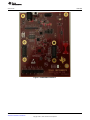
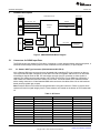
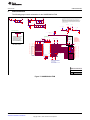
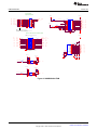
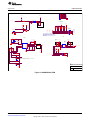
User's Guide
SLLU204 – June 2014
SN65DSI86/SN65DSI96 EVM User’s Manual
This guide describes how to use and configure the SN65DSI86 or SN65DSI96 EVM, with
recommendations for system hardware implementation. These recommendations are only guidelines; the
designer is responsible for all system characteristics and requirements. Refer to the datasheet for
technical details such as device operation and terminal description.
1
2
3
4
5
6
7
Contents
Overview ...................................................................................................................... 3
1.1
What are SN65DSI86 and SN65DSI96? ........................................................................ 3
1.2
What is the SN65DSIX6 EVM? ................................................................................... 3
1.3
What is Included in the SN65DSIX6 EVM? ..................................................................... 3
1.4
What does the EVM look like? .................................................................................... 4
Hardware Description ....................................................................................................... 6
2.1
Connectors for DSIX6 Input Ports ................................................................................ 6
2.2
Connectors for DSIX6 Output Ports .............................................................................. 8
2.3
I2C................................................................................................................... 10
2.4
Enable and Reset ................................................................................................. 10
2.5
Power ............................................................................................................... 10
2.6
Ambient Light Sensor ............................................................................................. 11
2.7
Reference CLK Programmability ................................................................................ 11
2.8
DIP Switch Configuration ......................................................................................... 11
Quick Start Guide .......................................................................................................... 12
References .................................................................................................................. 12
EVM Bill of Materials ....................................................................................................... 12
EVM Schematics ........................................................................................................... 15
Sample Total Phase Aardvark I2C Host Adapter Scripts ............................................................. 19
7.1
1920x1080 @60Hz 24bpp – DSI A Channel Only and 2 DP at HBR ...................................... 19
7.2
2560x1440 @60Hz 24bpp – Dual DSI Channels and 2 DP at HBR2 ...................................... 21
7.3
Enabling ASSR in Panel.......................................................................................... 23
List of Figures
...........................................................................................
1
SN65DSIX6EVM Rev1 or Rev2
2
SN65DSI8X EVM Rev 3 .................................................................................................... 5
3
SN65DSIX6 EVM Block Diagram .......................................................................................... 6
4
DSI86 EDP_30PIN
5
DSI86 EDP_40PIN ......................................................................................................... 10
6
DSI86/96 Rev1 EVM Example Setup .................................................................................... 12
7
SN65DSI86/96 EVM ....................................................................................................... 15
8
SN65DSI86/96 EVM ....................................................................................................... 16
9
SN65DSI86/96 EVM ....................................................................................................... 17
10
SN65DSI86/96 EVM ....................................................................................................... 18
11
SN65DSI86/96 EVM ....................................................................................................... 19
..........................................................................................................
4
9
List of Tables
1
SN65DSIX6 Features Summary ........................................................................................... 3
2
J4 Pin-out ..................................................................................................................... 6
SLLU204 – June 2014
Submit Documentation Feedback
SN65DSI86/SN65DSI96 EVM User’s Manual
Copyright © 2014, Texas Instruments Incorporated
1
www.ti.com
2
3
J1 Pin-out ..................................................................................................................... 7
4
J1 Pin-out ..................................................................................................................... 8
5
J6 and J9 Selection Options
6
J6 Pin-out ..................................................................................................................... 8
7
DIP Switch Settings ........................................................................................................ 11
8
EVM Bill of Materials ....................................................................................................... 12
...............................................................................................
SN65DSI86/SN65DSI96 EVM User’s Manual
Copyright © 2014, Texas Instruments Incorporated
8
SLLU204 – June 2014
Submit Documentation Feedback
Overview
www.ti.com
1
Overview
1.1
What are SN65DSI86 and SN65DSI96?
The SN65DSI86 and SN65DSI96 devices are referred to as SN65DSIX6 in this document. SN65DSIX6 is
a MIPI DSI to eDP bridge device that supports video modes in forward direction. The SN65DSIX6 targets
portable applications such as tablets and smart phones that utilize the MIPI DSI video format. The
SN65DSIX6 can be used between a GPU with DSI output and a video panel with DisplayPort inputs.
Both devices share the same pin out and package.
Table 1 is a summary of the feature sets on these devices:
Table 1. SN65DSIX6 Features Summary
Part Name
1.2
Description
SN65DSI86
Dual channel DSI to 4 eDP lanes
SN65DSI96
Dual channel DSI to 4 eDP lane with adaptive display
technology
What is the SN65DSIX6 EVM?
The SN65DSIX6 EVM is a PCB created to help customers evaluate the SN65DSIX6 device for video
applications with the DSI and DisplayPort interface. This EVM can also be used as a hardware reference
design for any implementation of the SN65DSIX6. The SN65DSIX6 EVM is designed for both the
SN65DSI86 and SN65DSI96 DSI bridge devices.
NOTE: Note: Some portions and components in the EVM or in this document may include the
references to SN65DSI86 instead of addressing both part numbers. For the purposes of this
document, the SN65DSI86 is interchangeable with the SN65DSI96.
PCB design and layout files are provided upon request to aid the PCB design with a SN65DSIX6
component. The layout files are a guideline for implementing the SN65DSIX6, with illustrations of the
routing and placement rules. The EVM design includes test components to evaluate the SN65DSIX6
which may not applicable for production.
1.3
What is Included in the SN65DSIX6 EVM?
The major components of the EVM are:
• SN65DSI86ZQE or SN65DSI96ZQE
• Samtec QSH type connectors on DSI and eDP interfaces
• Standard DisplayPort connector
• Hirose type connector on DSI Ch A interface
• I2C programming interface for an external I2C host connection
SLLU204 – June 2014
Submit Documentation Feedback
SN65DSI86/SN65DSI96 EVM User’s Manual
Copyright © 2014, Texas Instruments Incorporated
3
Overview
1.4
www.ti.com
What does the EVM look like?
Figure 1. SN65DSIX6EVM Rev1 or Rev2
4
SN65DSI86/SN65DSI96 EVM User’s Manual
Copyright © 2014, Texas Instruments Incorporated
SLLU204 – June 2014
Submit Documentation Feedback
Overview
www.ti.com
Figure 2. SN65DSI8X EVM Rev 3
SLLU204 – June 2014
Submit Documentation Feedback
SN65DSI86/SN65DSI96 EVM User’s Manual
Copyright © 2014, Texas Instruments Incorporated
5
Hardware Description
2
www.ti.com
Hardware Description
DSI Input
eDP Output
SN65DSI86/96 EVM
Berger
2 x 16
AUXP/N
DSI_CHA_CLK
ML[3:0]P/N
DSI_CHA_DATAP/N[3:0]
or
SMA/
Samtec
DP
DSI_CHB_CLK
DSI86/96
DSI_CHB_DATAP/N[3:0]
Page 2
or
HPD
Samtec
Page 3
Page 3
3.3 V
5V–
17 V
1.2 V
Ambient
Light
Ref_CLK IN
Page 5
1.8 V
Page 6
I2C Logic
Reset
Logic
Page 4
Page 4
CDC-RefCLK
Generation
Page 4
Figure 3. SN65DSIX6 EVM Block Diagram
2.1
Connectors for DSIX6 Input Ports
The EVM has two input options for DSI video. If designing a custom breakout board using these options, a
schematic and an allegro PCB symbol for either connector can be provided by TI upon request.
2.1.1
J4 - Samtec QSH Type Connector (P/N QSH-020-01-H-D-DP-A)
J4 is a Samtec QSH-type connector that can be mated with a matching QTH type connector on the top.
The J4 provides DSI input connections to both DSI Ch A and Ch B signals, and access to I2C and other
miscellaneous signals such as IRQ. XC connections are open vias if a connection to other signals is
required. The mating connector part number is QTH-020-01-H-D-DP-A. For an SMA type connection, a
HDR-128291-XX breakout board from Samtec can be used. The HDR-128291-XX is a breakout board
with a mating connector to J4 and standard SMA male connectors via cables. More info on this breakout
board can be provided upon request.
Note: Resistors R6 thru R15 should be unpopulated when using this connector. Failure to remove these
resistors will result in signal integrity issues. These resistors are located on the bottom of PCB underneath
J4.
Table 2. J4 Pin-out
6
Pin#
Name
Pin#
Name
1
DSI_A3P
2
DSI_B3P
3
DSI_A3N
4
DSI_B3N
5
GND
6
GND
7
GND
8
GND
9
DSI_A2P
10
DSI_B2P
11
DSI_A2N
12
DSI_B2N
13
GND
14
GND
15
GND
16
GND
17
DSI_ACLKP
18
DSI_BCLKP
19
DSI_ACLKN
20
DSI_BCLKN
21
GND
22
GND
SN65DSI86/SN65DSI96 EVM User’s Manual
Copyright © 2014, Texas Instruments Incorporated
SLLU204 – June 2014
Submit Documentation Feedback
Hardware Description
www.ti.com
Table 2. J4 Pin-out (continued)
2.1.2
Pin#
Name
Pin#
Name
23
GND
24
GND
25
DSI_A1P
26
DSI_B1P
27
DSI_A1N
28
DSI_B1N
29
GND
30
GND
31
GND
32
GND
33
DSI_A0P
34
DSI_B0P
35
DSI_A0N
36
DSI_B0N
37
RESETN
38
IRQ
39
I2C_SDA
40
I2C_SCL
J1 – Hirose FX Type Connector (P/N FX6A-40S-0.8SV2)
J1 is a Hirose FX-type connector that can be mated with a matching FX plug on the top. The part number
for the mating connector is FX6A-40P-0.8SV2. J1 provides a DSI input connection only to the DSI Ch A
signals. J1 also provides access to I2C and other miscellaneous signals such as IRQ. This connector is
only available in Revision 1 and 2 of the EVM.
Table 3. J1 Pin-out
2.1.3
Pin#
Name
Pin#
Name
1
NC
2
NC
3
NC
4
NC
5
NC
6
NC
7
NC
8
NC
9
GND
10
NC
11
DSI_ACLKP
12
GND
13
DSI_ACLKN
14
NC
15
GND
16
NC
17
DSI_A0P
18
I2C_SCL
19
DSI_A0N
20
I2C_SDA
21
GND
22
GND
23
DSI_A1P
24
IRQ
25
DSI_A1N
26
NC
27
GND
28
NC
29
DSI_A2P
30
NC
31
DSI_A2N
32
GND
33
GND
34
NC
35
DSI_A3P
36
NC
37
DSI_A3N
38
NC
39
GND
40
GND
J1 – 100-mil Male Header
J1 is a 2x16 100-mil male header. J1 provides DSI input connection only to the DSI Ch A signals. J1 also
provides access to I2C and other miscellaneous signals such as IRQ. This connector is only available in
Revision 3 of the EVM.
SLLU204 – June 2014
Submit Documentation Feedback
SN65DSI86/SN65DSI96 EVM User’s Manual
Copyright © 2014, Texas Instruments Incorporated
7
Hardware Description
www.ti.com
Table 4. J1 Pin-out
2.2
Pin#
Name
Pin#
1
GND
2
Name
GND
3
DSI_A0N
4
I2C_SCL
5
DSI_A0P
6
I2C_SDA
7
GND
8
GND
9
DSI_A1N
10
IRQ
11
DSI_A1P
12
NC
13
GND
14
GND
15
DSI_A2N
16
NC
17
DSI_A2P
18
NC
19
GND
20
GND
21
DSI_A3N
22
NC
23
DSI_A3P
24
NC
25
GND
26
GND
27
DSI_ACLKN
28
NC
29
DSI_ACLKP
30
NC
31
GND
32
GND
Connectors for DSIX6 Output Ports
There are two output port options available on the EVM for the DisplayPort output signals. By default, the
DisplayPort interface signals from the SN65DSIX6 are connected to the J9 connector. To use the J6,
follow these capacitor select options:
Table 5. J6 and J9 Selection Options
Component Install Requirement
2.2.1
J6
C63, C64, C65, C66, C67, C68, C69, C70, C71, C72
J9 (Default)
C73, C74, C75, C76, C77, C78, C79, C80, C81, C82
J9 – Standard DisplayPort Male Connectors (Molex P/N 47272-0001)
J9 is a standard DisplayPort male connector widely used in notebooks and desktops for interfacing to
external DisplayPort capable monitors. DisplayPort cables for connecting to this connector and a external
monitor can be obtained from a third party source.
2.2.2
J6 - Samtec QSH type Connector (P/N QSH-020-01-H-D-DP-A)
J6 is a Samtec QSH-type connector that can be mated with a matching QTH-type connector on the top.
The J6 provides DSI input connections to DisplayPort signals and accesses the back light power and its
related signals. XC connections are open vias if a connection to other signals is required. The mating
connector part number is QTH-020-01-H-D-DP-A. For an SMA-type connection, a HDR-128291-XX
breakout board from Samtec can be used. The HDR-128291-XX is a breakout board with a mating
connector to J6 and standard SMA male connectors via cables. More info on this breakout board can be
obtained from the Samtec website.
Table 6. J6 Pin-out
Pin#
8
Name
Pin#
Name
1
ML3N
2
I2C_SDL (LVCMOS 3.3V
Level)
3
ML3P
4
I2C_SDA (LVCMOS 3.3V
Level)
5
GND
6
GND
SN65DSI86/SN65DSI96 EVM User’s Manual
Copyright © 2014, Texas Instruments Incorporated
SLLU204 – June 2014
Submit Documentation Feedback
Hardware Description
www.ti.com
Table 6. J6 Pin-out (continued)
2.2.2.1
Pin#
Name
Pin#
Name
7
GND
8
GND
LCD_VCC
9
ML2N
10
11
ML2P
12
LCD_VCC
13
GND
14
EDP SELF TEST
15
GND
16
HPD
17
ML1N
18
NC
19
ML1P
20
NC
21
GND
22
BL_ENABLE
23
GND
24
PWM_DIM
25
ML0N
26
NC
27
ML0P
28
NC
29
GND
30
GND
31
GND
32
GND
33
AUXP
34
BL_PWR
35
AUXN
36
BL_PWR
37
GND
38
BL_PWR
39
GND
40
BL_PWR
J6 Daughterboards
There are two daughterboards for connecting to eDP panels: DSI86 EDP_30PIN and DSI86 EDP_40PIN.
These boards are not provided with the SN65DSI86/96 EVM board, but are available upon request.
2.2.2.1.1
DSI86 EDP_30PIN
The DSI86 EDP_30PIN daughterboard supports up to 2 eDP lanes. This board is intended to mate to an
eDP panel that has a pin-out that matches Table 6-3 in the VESA Embedded DisplayPort Standard
Version 1.3. This board has a Samtec QTH-020-01-H-D-DP-A for mating to J6 on the SN65DSI86/96 EVM
board and an IPEX receptacle (part# 20455-030E-02) for interfacing to an eDP panel. The ribbon cable for
connecting the eDP panel to this daughterboard should use a IPEX plug (part# 20453-030T-11S) or
equivalent.
Figure 4. DSI86 EDP_30PIN
SLLU204 – June 2014
Submit Documentation Feedback
SN65DSI86/SN65DSI96 EVM User’s Manual
Copyright © 2014, Texas Instruments Incorporated
9
Hardware Description
2.2.2.1.2
www.ti.com
DSI86 EDP_40PIN
The DSI86 EDP_40PIN daughterboard supports up to 4 eDP lanes. This board is intended to mate to an
eDP panel that has a pin-out that matches Table 6-4 in the VESA Embedded DisplayPort Standard
Version 1.3. This board has a Samtec QTH-020-01-H-D-DP-A for mating to J6 on the SN65DSI86/96 EVM
board and an IPEX receptacle (part# 20455-040E-02) for interfacing to an eDP panel. The ribbon cable for
connecting the eDP panel to this daughterboard should use a IPEX plug (part# 20453-040T-11S) or
equivalent.
Figure 5. DSI86 EDP_40PIN
2.3
I2C
Access to I2C signals are provided via DSI input connectors J1, J4, J10, or J16. I2C signal levels should
be at 1.8 V when the I2C interface is accessed through connectors J1, J4, or J16. 3.3 V to 1.8 V voltage
translation is provided when an I2C host is connected through J10.
A standalone external I2C host can connect via J10 for debug purposes. An example of an external I2C
host controller is the Total Phase Aardvark I2C/SPI host adapter (Total Phase Part#: TP240141). Sample
scripts for this I2C Host controller are provided in Section 7.
2.4
Enable and Reset
There are three device enable and reset options for the EVM.
• Supervisor circuitry option: This is the default configuration. The enable (EN) signal is held low until
the power good (PG) from the 1.8V voltage regulator reaches a stable high voltage level, then the EN
is released high.
• RC timing option: The C10 external capacitor and internal resistor control the EN ramp time after the
device is powered on. C10 is a DNI (Do Not Install option) by default. C10 must be installed and R52
must be uninstalled to enable this option.
• External control option: A push-button (SW1) or a J16 pin 9 is available for the manual control of the
EN signal.
2.5
Power
The 5 V-17 V power supply can be used to operate the SN65DSIX6 EVM. A plug to accept a 5 V to 17 V
wall power adapter is provided on the EVM (J13).
The EVM is designed to accommodate a maximum current of 1.5 A. The current consumption of the board
without the back light driver enabled is about 75 mA + SN65DSIX6 device power. The SN65DSIX6
consumes about 23 mW at power on, and up to 320 mW depending on the system configurations. The
total power consumption of the board could vary depending on the LCD panels when the on-board back
light driver is used. When an LCD panel consumes more current than 1.5 A minus 75 mA + SN65DSIX6
device power, the external back light source should be used.
10
SN65DSI86/SN65DSI96 EVM User’s Manual
Copyright © 2014, Texas Instruments Incorporated
SLLU204 – June 2014
Submit Documentation Feedback
Hardware Description
www.ti.com
Important: Do not plug in any power source higher than the configured voltage (17-V).
2.6
Ambient Light Sensor
The SN65DSIX6 EVM incorporates a TAOS TSL2561T ambient light sensor. An external GPU can use
this sensor with the SN65DSI96. By default, the sensor is located at the I2C slave address of 0x29 (R188
installed and R189 uninstalled). The I2C slave address can be changed to 0x49 (uninstall R188 and install
R189) or 0x39 by (uninstall R188 and uninstall R189).
2.7
Reference CLK Programmability
The SN65DSIX6 EVM incorporates programmable CLK circuitry using TI-programmable device
CDCEL913. The output of the CDCEL913 is connected to the reference CLK of the SN65DSIX6. The CLK
can be programmed via I2C signals brought out to on-board connectors J9, J12 or J10. When J10 is used,
jumpers should be placed on J9 and J12. The default frequency of the REFCLK is set to 27MHz.
2.8
DIP Switch Configuration
The DIP switch lets the user operate the device and EVM in different configurations. When the switch is in
an open position, the corresponding signal is tied high. When the switch is in ON (closed) position, the
corresponding signal is tied to GND.
Table 7. DIP Switch Settings
DEFAULT CONFIG
DIP SW No
Signal Name
Description
Open(Off) HIGH
GPIO1
General Purpose I/O.
Defaults to Input. Also
used to select REFCLK
frequency.
X
SW2-2
GPIO2
General Purpose I/O.
Defaults to Input. Also
used to select REFCLK
frequency.
X
SW2-3
GPIO3
General Purpose I/O.
Defaults to Input. Also
used to select REFCLK
frequency.
SW2-4
GPIO4
General Purpose I/O.
Defaults to Input. Also
used to select REFCLK
frequency.
SW2-1
Closed(On) LOW
X
X
Sets the I2C slave
address of the
SN65DSIX6 by
controlling the ADDR
pin.
High = 0x2D (default)
Low = 0x2C
SW2-5
ADDR
SW2-6
TEST1
Reserved. Texas
Instruments use only
X
SW2-7
TEST2
Reserved. Texas
Instruments use only.
For DP compliance
testing make dip switch
position to OFF (high).
X
SW2-8
I2C_3V3EN
Enables 3.3V voltage
translator for the I2C
signals
SLLU204 – June 2014
Submit Documentation Feedback
X
X
SN65DSI86/SN65DSI96 EVM User’s Manual
Copyright © 2014, Texas Instruments Incorporated
11
Quick Start Guide
3
www.ti.com
Quick Start Guide
1. Plug in a DSI source to J1 or J4. Refer to Section 2.1 for details on these connectors. All used DSI
inputs should be held at LP11 state during this step.
2. Plug in a DisplayPort video sink device on J9 (Standard DisplayPort connector) or J6 (eDP breakout
connector). Refer to Section 2.2 for details on these connectors.
3. Plug in an I2C host on J10 if using an external I2C host.
4. Correctly configure the DIP switch setting.
5. Apply power to the EVM. The following LEDS should light up: D3 and D6. D1 may light up depending
on the configuration.
6. Configure the device for the desired mode of operation via I2C. Example Aardvark scripts are provided
in Section 7.
7. Start video streaming on the DSI input.
8. Video output should be observed after the configuration is complete.
Figure 6. DSI86/96 Rev1 EVM Example Setup
4
References
SN65DSIX6 Datasheet.
5
EVM Bill of Materials
Table 8. EVM Bill of Materials
Item
12
Quantity
Reference
Part
1
7
C1, C38, C39, C42,
C45, C46, C57
10uF
2
5
C2, C11, C28, C83,
C91
1.0uF
SN65DSI86/SN65DSI96 EVM User’s Manual
Copyright © 2014, Texas Instruments Incorporated
Manuf
Manuf PN
SLLU204 – June 2014
Submit Documentation Feedback
EVM Bill of Materials
www.ti.com
Table 8. EVM Bill of Materials (continued)
Item
Quantity
Reference
Part
3
21
C3, C4, C6, C7, C9,
C56, C59, C61,
C62, C73, C74,
C75, C76, C77,
C78, C79, C80,
C81, C82, C89, C90
Manuf
Manuf PN
0.1uF
4
4
C5, C8, C58, C60
0.01uF
5
12
C10, C63, C64,
C65, C66, C67,
C68, C69, C70,
C71, C72, C84
DNI
6
1
C22
220pF
7
10
C23, C29, C30,
C31, C32, C33,
C85, C86, C87, C88
0.1uF
8
1
C24
18pF
9
5
C25, C26, C44,
C48, C55
DNI
10
2
C27, C37
22uF
11
1
C35
10uF
Murata
GRM21BR61E106K
A73L
12
1
C36
22uF
Murata
GRM31CR61E226K
E15L
13
1
C40
3.3nF
14
2
C43, C47
0.01uF
15
1
D1
LED Orange 0805
Rohm
SML-211DTT86
16
1
D3
LED Green 0805
Arrow (Lumex)
670-1006
(SML_LX0805GC)
17
18
1
D6
LED RED 0805
Rohm
SML-211UT
1
D8
20V, 1A
Comchip
CDBA120SL-G
19
1
FB4
220 @ 100MHZ
Murata
BLM18EG221SN1D
20
1
J1
2x16 Male Header
Sullins
PBC16DAAN
QSH-020-01
Samtec
QSH-020-01-X-DDP-A
21
2
J4, J6
22
3
J7, J8, J11
HDR2X1 M .1
AMP
103321-2
Molex
47272-0001
CUI STACK
PJ-202AH
23
1
J9
Display_Port_Conn
ector
24
1
J10
Header 5x2 0.1"
thru-hole
25
1
J13
2.1mm x 5.5mm
26
4
J14, J17, J20, J21
HDR2X1 M .1
27
1
J16
HEADER 1x10
28
2
J18, J19
HDR3X1 M .1
29
8
LP1, LP2, LP3,
LP4, LP5, LP6,
LP7, LP9
LP
KOBIKONN
151-103-RC
30
1
L1
2.2uH
Vishay
IHLP1616ABER2R2
M11
31
2
R1, R53
1K
32
2
R1, R53
350
16
R3, R4, R54, R55,
R56, R57, R58,
R59, R60, R61,
R77, R78, R79,
R87, R188, R191
4.7K
33
SLLU204 – June 2014
Submit Documentation Feedback
SN65DSI86/SN65DSI96 EVM User’s Manual
Copyright © 2014, Texas Instruments Incorporated
13
EVM Bill of Materials
www.ti.com
Table 8. EVM Bill of Materials (continued)
Item
Quantity
Reference
Part
34
1
R5
10nF
35
11
R6, R7, R8 ,R9,
R10, R11, R12,
R13, R14, R15, R70
0
36
7
R16, R51, R66,
R112, R116, R117,
R189
DNI
37
5
R27, R83, R113,
R114, R115
100K
38
14
R29, R52, R75,
R76, R80, R88,
R104, R108, R109,
R110, R111, R118,
R186, R187
0
39
2
R33, R36
1M
40
1
R67
18
41
5
R72, R73, R74,
R86, R103
10K
42
1
R81
500
43
1
R82
2.49K
44
1
R84
4.99K
45
1
R89
3.57K
46
1
R90
2.87K
47
1
R105
DNI
48
1
R192
4k
49
1
SW1
50
1
SW2
51
1
52
3
53
1
U1
SN65DSI86
TI
SN65DSI86ZQER
54
1
U2
SN74LVC1G07DCK
TI
SN74LVC1G07DCK
55
1
U3
TPS3808
TI
TPS3808g18DBVT
56
1
U4
SN74LVC1G08DCK
TI
SN74LVC1G08DCK
57
1
U5
CDCEL913PW
TI
CDCEL913PW
58
1
U6
TXS0102DCUT
TI
TXS0102DCUT
59
2
U8, U9
Manuf PN
PB_SWITCH
OMRON
B3SN-3012P
8-POS 50-MIL SMT
C&K(ITTCANNON)
TDA08H0SK1R
SW6
TS01CQE
C&K Div.
TS01CQE
TP1, TP5, TP6
T POINT S
TPS74201RGWT
TI
TPS74401RGWT
TI
SN74AVC1T45DCK
R
TSL2561T
60
2
U11, U12
SN74AVC1T45DCK
R
61
1
U13
TSL2561T
TAOS
62
1
U14
TPS62142RGTR
TI
TPS62142RGTR
ABRACON
ABM8-27.000MHZ10-1-U-T
63
14
Manuf
1
Y1
27MHZ _crystal
SN65DSI86/SN65DSI96 EVM User’s Manual
Copyright © 2014, Texas Instruments Incorporated
SLLU204 – June 2014
Submit Documentation Feedback
EVM Schematics
www.ti.com
6
EVM Schematics
The following pages contain schematics for the SN65DSI86/96 EVM.
BOARD_1P8V
LP1
LP2
Note: Bypass caps
should be placed near U1
SN65DSI86.
LP3
VCCIO
0
r0402
5%
VCC
BOARD_1P2V
LP7
R108
********Layout Notes*******
For all differential pairs(DSI and DisplayPort) in this design follow the guidelines decribed
below:
Route together with controlled differential 100ohm impedance and controlled single
ended 50ohm impedance. Keep away from other high speed signals especially all
MLxP/N* signals. Keep lengths within 5mil of each other. Keep traces on layers adjacent
to the ground plane. Keep the number of VIAS to minimum. If VIAS used, make it
symetrical through all signals. Keep diff pairs separated at least by x3 of the trace width.
NO STUBS on the signal path, components should be placed such that the signals can
routed in pass-thru manner.
R109
C1
10uF
C4
C6
C62
0.1uF
0.1uF
0.1uF
0
r0402
5%
C2
C3
C5
C7
1.0uF
0.1uF
0.01uF
0.1uF
LP9
VCCA
R110
C61
0.1uF
0
r0402
5%
C57
10uF
C11
C56
C58
C59
C60
1.0uF
0.1uF
0.01uF
0.1uF
0.01uF
BOARD_1P8V
SilkScreen:
BOARD_3P3V
IRQ
C9
TP1
T POINT S
R1
1K
5
0.1uF
2
IRQ
U2
SN74LVC1G07DCK
4
IRQ_OUT
3
1
350
r0402
5%
2
SilkScreen:
REF_CLK
IRQ
D1
IRQ_LED
Reset Implementation
BOARD_RESETN
SilkScreen:
R2
LED Orange 0805
J17
HDR2X1 M .1
1
C10
DNI
0.2uF
EXT_REFCLK
VCCIO
VCC
VCCA
*IMPORTANT*
If REFCLK is to be
used, the CLK trace
length between the
REFCLK terminal and
the source of the REF
CLK(OSC or Xtal)
should be kept as short
as possble.
r0402
R118
0
5%
BOARD_1P8V
BOARD_1P8V
R104 and R105
have a shared
footprint node
Vpll
Vccio
Vccio
BOARD_RESETN
A1
PG4
ADDR
PG4
PG4
TEST1
TEST2
PG3
PG3
PG3
PG3
PG3
PG3
PG3
PG3
PG3
PG3
DSI_A0P
DSI_A0N
DSI_A1P
DSI_A1N
DSI_A2P
DSI_A2N
DSI_A3P
DSI_A3N
DSI_ACLKP
DSI_ACLKN
PG3
PG3
PG3
PG3
PG3
PG3
PG3
PG3
PG3
PG3
DSI_B0P
DSI_B0N
DSI_B1P
DSI_B1N
DSI_B2P
DSI_B2N
DSI_B3P
DSI_B3N
DSI_BCLKP
DSI_BCLKN
B3
B5
H3
J3
H4
J4
H6
J6
H7
J7
H5
J5
DSI_B0P
DSI_B0N
DSI_B1P
DSI_B1N
DSI_B2P
DSI_B2N
DSI_B3P
DSI_B3N
DSI_BCLKP
DSI_BCLKN
C2
C1
D2
D1
F2
F1
G2
G1
E2
E1
REFCLK
ADDR
SCL
SDA
TEST1
TEST2
IRQ
DA0P
DA0N
DA1P
DA1N
DA2P
DA2N
DA3P
DA3N
DACP
DACN
ML3N
ML3P
ML2N
ML2P
ML1N
ML1P
ML0N
ML0P
DB0P
DB0N
DB1P
DB1N
DB2P
DB2N
DB3P
DB3N
DBCP
DBCN
AUXP
AUXN
HPD
GPIO4
GPIO3
GPIO2
GPIO1
A8
D8
E4
E5
F4
F5
F6
G8
DSI INPUT
DSI_A0P
DSI_A0N
DSI_A1P
DSI_A1N
DSI_A2P
DSI_A2N
DSI_A3P
DSI_A3N
DSI_ACLKP
DSI_ACLKN
EN
GND
GND
GND
GND
GND
GND
GND
GND
PG3,4
B1
R3
4.7K
A9
G9
E6
B2
H2
0.01uF
R4
4.7K
R105
DNI
r0402
1%
Vcca
Vcca
Vcca
Vcca
Vcca
C8
0.1uF
D6
D5
J2
J9
C90
1.0uF
Vcc
Vcc
Vcc
Vcc
C91
D9
B6
A2
VDDPLL
U1
ADDR = 1, Slave Addr = 0x2D (0101101)
ADDR = 0, Slave Addr = 0x2C (0101100)
Place as near
as possible to
REFCLK
terminal on U1
SN65DSI86/96
Reset(EN) can be implemented with passive
components as shown or active circuitry. In
case of using passive components, the
values of the RC circuitry need to be
adjusted to make sure the low to high
transition occurs after the Vcc supply has
reached the minimum recommended
operating voltage. For this reason, it is
recommended to USE ACTIVE CIRCUITRY for
better control of the RESET/EN timing.
NC
A7
0
RREFCLK
R104
H1
J1
I2C_SCL
I2C_SDA
A3
IRQ
IRQ
r0402
5%
REFCLK
PG4
PG3,4
PG3,4
PG3
B9
B8
ML3N
ML3P
C63
DNI
C64
DNI
EDP_ML3N
EDP_ML3P
PG3
PG3
C9
C8
ML2N
ML2P
C65
DNI
C66
DNI
EDP_ML2N
EDP_ML2P
PG3
PG3
E9
E8
ML1N
ML1P
C67
DNI
C68
DNI
EDP_ML1N
EDP_ML1P
PG3
PG3
F9
F8
ML0N
ML0P
C69
DNI
C70
DNI
EDP_ML0N
EDP_ML0P
PG3
PG3
AUXP
AUXN
C71
DNI
C72
DNI
EDP_AUXP
EDP_AUXN
0.1uF
C74
0.1uF
DP_ML3N
DP_ML3P
PG3
PG3
C75
0.1uF
C76
0.1uF
DP_ML2N
DP_ML2P
PG3
PG3
C77
0.1uF
C78
0.1uF
DP_ML1N
DP_ML1P
PG3
PG3
0.1uF
C80
0.1uF
DP_ML0N
DP_ML0P
PG3
PG3
0.1uF
C82
0.1uF
DP_AUXP
DP_AUXN
PG3
PG3
H8
H9
J8
RHPD
R111
0
B4
A6
A5
A4
HPD
GPIO4
GPIO3
GPIO2
GPIO1
B7
AMUX
PG3,4
PG3,4
PG4
PG4
C73
XC17
C84
SN65DSI86
PG3,4
C79
DNI
R5
10nF
C81
PG3
PG3
ES1 Device:
- R111 populate with 0-ohm resistor
- R5 populate with 10nF capacitor.
Production Device:
- R111 populate with 51K 1% resistor
- R5 should be a DNI
SN65DSI86/96
SIZE
C
SCALE: NONE
DWG NO:
T uesday, March 26, 2013
Sheet
2
of 6
Figure 7. SN65DSI86/96 EVM
SLLU204 – June 2014
Submit Documentation Feedback
SN65DSI86/SN65DSI96 EVM User’s Manual
Copyright © 2014, Texas Instruments Incorporated
15
EVM Schematics
www.ti.com
DSI ChA Display
Expansion Connector
BOARD_9V
BOARD_3P3V
J1
PG2,3
PG2,3
DSI_A0N
DSI_A0P
PG2,3
PG2,3
DSI_A1N
DSI_A1P
PG2,3
PG2,3
DSI_A2N
DSI_A2P
PG2,3
PG2,3
DSI_A3N
DSI_A3P
PG2,3
PG2,3
DSI_ACLKN
DSI_ACLKP
R9
0 R8
0
R11
0 R10
0
R13
0 R12
0
R15
0 R14
0
R7
0 R6
0
1
3
5
7
9
11
13
15
17
19
21
23
25
27
29
31
FX_N0
FX_P0
r0201
r0201
FX_N1
FX_P1
r0201
r0201
FX_N2
FX_P2
r0201
r0201
FX_N3
FX_P3
r0201
r0201
FX_CLKN
FX_CLKP
r0201
r0201
1
3
5
7
9
11
13
15
17
19
21
23
25
27
29
31
2
4
6
8
10
12
14
16
18
20
22
24
26
28
30
32
J6
2
4
6
8
10
12
14
16
18
20
22
24
26
28
30
32
R114
100K
J20
I2C_SCL
I2C_SDA
R16
DNI
r0402
IRQ
PG2,3,4
PG2,3,4
2
PG2,3
1
40
38
36
34
32
30
28
26
24
22
20
18
16
14
12
10
8
6
4
2
EDP_BL_PWR
HDR2X1 M .1
EDP_PWM_DIM
EDP_BL_ENABLE
BOARD_3P3V
R192
4K
J21
2
2x16 Header Male
1
HDR2X1 M .1
PG4,5
PG4,5
HPD
EDP_SELF_TEST
EDP_LCD_VCC
I2C_SDA_3P3V
I2C_SCL_3P3V
R116
R117
DNI
DNI
39
37
35
33
31
29
27
25
23
21
19
17
15
13
11
9
7
5
3
1
C_EDPTX_AUXN
C_EDPTX_AUXP
C_EDPTX_LN0P
C_EDPTX_LN0N
C_EDPTX_LN1P
C_EDPTX_LN1N
C_EDPTX_LN2P
C_EDPTX_LN2N
C_EDPTX_LN3P
C_EDPTX_LN3N
EDP_AUXN
EDP_AUXP
PG2
PG2
EDP_ML0P
EDP_ML0N
PG2
PG2
EDP_ML1P
EDP_ML1N
PG2
PG2
EDP_ML2P
EDP_ML2N
PG2
PG2
EDP_ML3P
EDP_ML3N
PG2
PG2
G3
G4
G1
G2
TOP
R115
100K
QSH-020-01
NOTE:
- Remove R6-R15 for DSI source connected to J4
- Populate R6-R15 w hen a source connected through J1
**R6 - R15 to be placed as near as J4 to avoid stub w hen J1 is not in use**
Samtec to SMA Connector for DSIA and DSIB
NOTE:
Add mounting holes as instructed in the layout notes.
J4
PG2,3,4
PG2,3
PG2
PG2
I2C_SCL
IRQ
DSI_B0N
DSI_B0P
PG2
PG2
DSI_B1N
DSI_B1P
PG2
PG2
DSI_BCLKN
DSI_BCLKP
PG2
PG2
DSI_B2N
DSI_B2P
PG2
PG2
DSI_B3N
DSI_B3P
0
r0201
R70
BOARD_3P3V
QSH-020-01
40
38
36
34
32
30
28
26
24
22
20
18
16
14
12
10
8
6
4
2
39
37
35
33
31
29
27
25
23
21
19
17
15
13
11
9
7
5
3
1
R29
I2C_SDA
PG2,3,4
BOARD_RESETN
PG2,4
DSI_A0N
PG2,3
DSI_A0P
PG2,3
0
DSI_A1N
DSI_A1P
DSI_ACLKN
DSI_ACLKP
PG2,3
PG2,3
PG2,3
PG2,3
DSI_A2N
DSI_A2P
PG2,3
PG2,3
DSI_A3N
DSI_A3P
PG2,3
PG2,3
J9
G3
G4
G1
G2
TOP
NOTE:
This connector is to interface DSI interface
w ith any source w ith SMA connectors via
Samtec to SMA cable
DPTX_GND
24
23
22
21
C83
R33
1M
r0402
5%
BOARD_3P3V
BOARD_1P8V
C85
DP_PWR
RTN
HPD
AUX_n
GND6
AUX_p
GND5
CAD
ML_3n
GND4
ML_3p
ML_2n
GND3
ML_2p
ML_1n
GND2
GND10 ML_1p
GND9
ML_0n
GND8
GND1
GND7
ML_0p
20
19
18
17
16
15
14
13
12
11
10
9
8
7
6
5
4
3
2
1
R112
DNI
R27
100K
r0402
HPD
DP_AUXN
PG2,4
PG2
DP_AUXP
PG2
DPTX_CAD
DP_ML3N
PG2
DP_ML3P
DP_ML2N
PG2
PG2
DP_ML2P
DP_ML1N
PG2
PG2
DP_ML1P
DP_ML0N
PG2
PG2
DP_ML0P
PG2
Display _Port_Connector_Source
1.0uF
R36
1M
r0402
5%
R113
100K
C86
0.1uF
0.1uF
U11
R186
EDP_BL_ENABLE
1
0
r0402
5%
3
EDP_BL_ENABLE_R
6
VCCA VCCB
A
5
DIR
4
B
GPIO3
PG2,4
GPIO4
PG2,4
2
GND
SN74AVC1T45DCKR
DIR L = B to A
DIR H = A to B
BOARD_3P3V
BOARD_1P8V
C87
C88
0.1uF
0.1uF
U12
R187
EDP_PWM_DIM
1
0
r0402
5%
EDP_PWM_DIM_R
3
5
VCCA VCCB
A
DIR
B
GND
6
4
2
SN74AVC1T45DCKR
DIR L = B to A
DIR H = A to B
Figure 8. SN65DSI86/96 EVM
16
SN65DSI86/SN65DSI96 EVM User’s Manual
Copyright © 2014, Texas Instruments Incorporated
SLLU204 – June 2014
Submit Documentation Feedback
EVM Schematics
www.ti.com
J16
1
2
3
4
5
6
7
8
9
10
RESET
BOARD_1P8V
BOARD_1P8V
R51
DNI
r0402
5%
PG2,3
BOARD_RESETN
BOARD_RESETN
GPIO1
GPIO2
GPIO3
GPIO4
ADDR
I2C_SDA
I2C_SCL
r0402
U3
RESET#
GND
MR#
VDD
SENSE
CT
6
5
4
CT
DIPSW
C22
C23
220pF
0.1uF
BOARD_1P8V
BOARD_1P8V
Note: Place caps
near the part.
R54
4.7K
r0402
5%
U4
SN74LVC1G08DCK
5
1
PG
BOARD_3P3V
BOARD_1P8V
R53
1K
r0402
5%
Vcc
R55
4.7K
r0402
5%
R56
4.7K
r0402
5%
R57
4.7K
r0402
5%
R58
4.7K
r0402
5%
R59
4.7K
r0402
5%
R60
4.7K
r0402
5%
R61
4.7K
r0402
5%
4
2
SW1
PB_SWITCH
1
2
PG2
PG2
PG2,3
PG2,3
PG2
PG2
PG2
3
4
3
N.O.
C24
18pF
SilkScreen:
PG2,3
HEADER 1x10
1
2
3
RESET#
R52
0
TPS3808
TPS3808g18DBVT
PG6
HPD
BOARD_RESETN
RESET
GPIO1
GPIO2
GPIO3
GPIO4
ADDR
TEST1
TEST2
I2C_3V3EN
TEST1 and TEST2 for Texas Instruments internal use
only. TEST1 shall be left unconnected or tied to
GND. TEST2 shall be left unconnected or tied to
GND. For DP compliance testing, TEST2 needs to be
pulled up to 1.8V.
SW2
8-POS 50-MIL SMT
C&K (ITT-CANNON)
TDA08H0SK1R
16
1
15
2
14
3
13
4
12
5
11
6
10
7
9
8
SilkScreen:
GPIO1
GPIO2
GPIO3
GPIO4
ADDR
TEST1
TEST2
I2C_3V3EN
I2C
CDC
C25
CDC_XIN
DNI
R66
DNI
r0402
5%
FB4
220 @ 100MHZ
CDC_XOUT
2
13
12
BOARD_1P8V
XOUT
VDD
VDDOUT
VDDOUT
VCTR
Y1
S0
S1_SDA
S2_SCL
Y2
CDCEL913PW
GND
GND
4
XIN_CLK
R74
10K
r0402
5%
CDC_VDD
6
7
11
R67
REFCLK
CDC_Y1
9
1
C28
C29
1.0uF
0.1uF
I2C_SDA_3P3V
I2C_SCL_3P3V
8
1
2
BOARD_3P3V
VCCB
VCCA
0.1uF
B1
B2
A1
A2
GND
OE
3
5
4
A1_SDA
A1_SCL
R75
R76
6
0
0
I2C_SDA
I2C_SCL
PG2,3
PG2,3
I2C_3V3EN
txs0102dcut
C31
C32
C33
0.1uF
0.1uF
0.1uF
C55
R77
4.7K
r0402
5%
SilkScreen:
R78
4.7K
r0402
5%
SilkScreen:
I2C
J10
2
1
3
5
7
9
CDC_S0
J8
1
C30
BOARD_3P3V
HDR2X1 M .1
CDC_S1_SDA
Note:
Place caps
near the
part.
7
PG2
PLACE CLOSE
TO U5
8
BOARD_1P8V
BOARD_3P3V
U6
18
r0402
1%
DNI
J7
CDC_S0
Y3
3
5
10
14
R73
10K
r0402
5%
C27
22uF
U5
1
DNI
R72
10K
r0402
5%
Note:
Place caps
near the
part.
BOARD_1P8V
Y1
27MHZ _cry stal
C26
PG3,5
PG3,5
2
I2C_SDA_3P3V
I2C_SCL_3P3V
2
4
6
8
10
GND
CDC_S1
Header 5x2 0.1" thru-hole
HDR2X1 M .1
1
2
3
I2C_SDA
SilkScreen:
CDC_SDA_ON
CDC_S2_SCL
GND
J18
HDR3X1 M .1
J11
1
2
NOTE:
SHUNT on CDC_SDA and CDC_SCL pin1 and 2 if external I2C host
via J10 for I2C programming of CDC device
CDC_S2
HDR2X1 M .1
1
2
3
I2C_SCL
SilkScreen:
CDC_SCL_ON
GND
J19
HDR3X1 M .1
RESET AND CDC
SIZE
C
SCALE: NONE
DWG NO:
Friday, September 06, 2013
Sheet
4
of 6
Figure 9. SN65DSI86/96 EVM
SLLU204 – June 2014
Submit Documentation Feedback
SN65DSI86/SN65DSI96 EVM User’s Manual
Copyright © 2014, Texas Instruments Incorporated
17
EVM Schematics
www.ti.com
BOARD_3P3V
BOARD_3P3V
R191
4.7K
r0402
5%
C89
0.1uF
TSL_INT
R189
DNI
r0402
5%
U13
1
5
3
VDD
SDA
SCL
6
4
I2C_SDA_3P3V
I2C_SCL_3P3V
2
TSL_A0
I2C_SDA_3P3V
I2C_SCL_3P3V
PG3,4
PG3,4
INT
GND
ASEL
TSL2561T
R188
4.7K
r0402
5%
I2C SLAVE ADDRESS:
0x29 or 0101001 (ASEL = 0)
0x39 or 0111001 (ASEL = float)
0x49 or 1000101 (ASEL = 1)
AMBIENT LIGHT SENSOR
SIZE
A
SCALE: NONE
DWG NO:
T hursday, November 01, 2012
Sheet
5
of 6
Figure 10. SN65DSI86/96 EVM
18
SN65DSI86/SN65DSI96 EVM User’s Manual
Copyright © 2014, Texas Instruments Incorporated
SLLU204 – June 2014
Submit Documentation Feedback
Sample Total Phase Aardvark I2C Host Adapter Scripts
www.ti.com
1.2V REGULATOR
SilkScreen:
ON
OFF
BOARD_9V
BOARD_3P3V
BOARD_1P2V
1
2
3
SW6
TS01CQE
2
D8
R81
500
r0402
5%
1 PWRIN_SW
J13
S
T
20V, 1A
2.1mm x 5.5mm
U8
5V to 17V
SilkScreen:
5
6
7
8
C39
10uF
R79
4.7K
r0402
5% EN1P2
D3
LED Green 0805
9V
10
11
IN
IN
IN
IN
PG
OUT
OUT
OUT
OUT
BIAS
EN
FB
C43
0.01uF
SS1P2
15
9
SS
PG1P2
R80
PG
0
1
20
19
18
R82
2.49K
r0402
1%
16
FB_1PT2V
NC
NC
NC
NC
NC
NC
GND
PAD
9V_DIODE
LED9V
2
3
1
2
3
4
13
14
17
12
21
TPS74201RGWT
C42
10uF
R84
4.99K
r0402
1%
C44
DNI
BOARD_9V
BOARD_3P3V
3.3V REGULATOR
BOARD_3P3V
BOARD_1P8V
LP6
1.8V REGULATOR
L1
R103
10K
r0402
5%
U14
C35
10uF
10
R86
10K
r0402
2
SW1
SW2
SW3
AVIN
VOS
13
SS_TR
J14
HDR2X1 M .1
PVIN1
PVIN2
9
8
C40
3.3nF
7
EN
PG
FB
SS_TR
DEF
FSW
PGND
PGND
AGND
AGND
1
2
3
SWOUT
2.2uH
14
4
PG3P3
R83
100K
r0402
5%
C37
22uF
C38
10uF
5
15
16
17
6
U9
R101
350
r0402
5%
5
6
7
8
C45
10uF
R87
4.7K
r0402
5% EN1P8
D6
LED RED 0805
1
11
PG
OUT
OUT
OUT
OUT
BIAS
EN
FB
C47
SilkScreen:
3P3V
TPS62142RGTR
10
IN
IN
IN
IN
0.01uF
SS1P8
15
NC
NC
NC
NC
NC
NC
GND
PAD
12
11
C36
22uF
SS
2
3
4
13
14
17
12
21
TPS74201RGWT
C48
DNI
9
PG1P8
R88
0
PG
PG
PG4
1
20
19
18
16
FB_1PT8V
R89
3.57K
r0402
1%
C46
10uF
R90
2.87K
r0402
1%
TO BE PLACED ACROSS PCB AS CONVENIENT
FOR OSCILLOSCOPE PROBE GROUNDS
SilkScreen:
GND SilkScreen:
TP5
T POINT S
SilkScreen:
GND
SilkScreen:
LP4
GND
TP6
T POINT S
GND
LP5
POWER
SIZE
C
SCALE: NONE
DWG NO:
T uesday, December 11, 2012
Sheet
6
of 6
Figure 11. SN65DSI86/96 EVM
7
Sample Total Phase Aardvark I2C Host Adapter Scripts
7.1
1920x1080 @60Hz 24bpp – DSI A Channel Only and 2 DP at HBR
<aardvark>
<configure i2c="1" spi="1" gpio="0" tpower="1" pullups="0" />
<i2c_bitrate khz="100" />
======Single 4 DSI lanes======
<i2c_write addr="0x2D" count="1" radix="16">10 26</i2c_write>
<sleep ms="10" />
======enhanced framing======
<i2c_write addr="0x2D" count="1" radix="16">5A 04</i2c_write>
<sleep ms="10" />
======Pre0dB 2 lanes no SSC======
<i2c_write addr="0x2D" count="1" radix="16">93 20</i2c_write>
SLLU204 – June 2014
Submit Documentation Feedback
SN65DSI86/SN65DSI96 EVM User’s Manual
Copyright © 2014, Texas Instruments Incorporated
19
Sample Total Phase Aardvark I2C Host Adapter Scripts
www.ti.com
<sleep ms="10" />
======L0mV HBR======
<i2c_write addr="0x2D" count="1" radix="16">94 80</i2c_write>
<sleep ms="10" />
======PLL ENABLE======
<i2c_write addr="0x2D" count="1" radix="16">0D 01</i2c_write>
<sleep ms="10" />
======POST2 0dB ======
<i2c_write addr="0x2D" count="1" radix="16">95 00</i2c_write>
<sleep ms="10" />
======Semi-Auto TRAIN ======
<i2c_write addr="0x2D" count="1" radix="16">96 0A</i2c_write>
<sleep ms="20" />
======ADDR 0x96 CFR======
<i2c_write addr="0x2D" count="0" radix="16">96</i2c_write>
<sleep ms="20" />
======Read======
<i2c_read addr="0x2D" count="1" radix="16">00</i2c_read>
<sleep ms="10" />
=====CHA_ACTIVE_LINE_LENGTH=======
<i2c_write addr="0x2D" count="2" radix="16">20 80 07</i2c_write>
<sleep ms="10" />
=====CHA_VERTICAL_DISPLAY_SIZE=======
<i2c_write addr="0x2D" count="2" radix="16">24 38 04</i2c_write>
<sleep ms="10" />
=====CHA_HSYNC_PULSE_WIDTH=======
<i2c_write addr="0x2D" count="2" radix="16">2C 10 80</i2c_write>
<sleep ms="10" />
=====CHA_VSYNC_PULSE_WIDTH=======
<i2c_write addr="0x2D" count="2" radix="16">30 0E 80</i2c_write>
<sleep ms="10" />
=====CHA_HORIZONTAL_BACK_PORCH=======
<i2c_write addr="0x2D" count="1" radix="16">34 98</i2c_write>
<sleep ms="10" />
=====CHA_VERTICAL_BACK_PORCH=======
<i2c_write addr="0x2D" count="1" radix="16">36 13</i2c_write>
<sleep ms="10" />
=====CHA_HORIZONTAL_FRONT_PORCH=======
<i2c_write addr="0x2D" count="1" radix="16">38 10</i2c_write>
20
SN65DSI86/SN65DSI96 EVM User’s Manual
Copyright © 2014, Texas Instruments Incorporated
SLLU204 – June 2014
Submit Documentation Feedback
Sample Total Phase Aardvark I2C Host Adapter Scripts
www.ti.com
<sleep ms="10" />
=====CHA_VERTICAL_FRONT_PORCH=======
<i2c_write addr="0x2D" count="1" radix="16">3A 03</i2c_write>
<sleep ms="10" />
======DP-18BPP Enable======
<i2c_write addr="0x2D" count="1" radix="16">5B 00</i2c_write>
<sleep ms="10" />
=====COLOR BAR =======
<i2c_write addr="0x2D" count="1" radix="16">3C 00</i2c_write>
<sleep ms="10" />
======enhanced framing and Vstream enable======
<i2c_write addr="0x2D" count="1" radix="16">5A 0C</i2c_write>
<sleep ms="10" />
</aardvark>
7.2
2560x1440 @60Hz 24bpp – Dual DSI Channels and 2 DP at HBR2
<aardvark>
<configure i2c="1" spi="1" gpio="0" tpower="1" pullups="0" />
<i2c_bitrate khz="100" />
======Dual 4 DSI lanes======
<i2c_write addr="0x2D" count="1" radix="16">10 00</i2c_write>
<sleep ms="10" />
======enhanced framing======
<i2c_write addr="0x2D" count="1" radix="16">5A 04</i2c_write>
<sleep ms="10" />
======Pre0dB 2 lanes no SSC======
<i2c_write addr="0x2D" count="1" radix="16">93 20</i2c_write>
<sleep ms="10" />
======L0mV HBR2======
<i2c_write addr="0x2D" count="1" radix="16">94 E0</i2c_write>
<sleep ms="10" />
======PLL ENABLE======
<i2c_write addr="0x2D" count="1" radix="16">0D 01</i2c_write>
<sleep ms="10" />
======POST2 0dB ======
<i2c_write addr="0x2D" count="1" radix="16">95 00</i2c_write>
<sleep ms="10" />
======Semi-Auto TRAIN ======
<i2c_write addr="0x2D" count="1" radix="16">96 0A</i2c_write>
<sleep ms="20" />
SLLU204 – June 2014
Submit Documentation Feedback
SN65DSI86/SN65DSI96 EVM User’s Manual
Copyright © 2014, Texas Instruments Incorporated
21
Sample Total Phase Aardvark I2C Host Adapter Scripts
www.ti.com
======ADDR 0x96 CFR======
<i2c_write addr="0x2D" count="0" radix="16">96</i2c_write>
<sleep ms="20" />
======Read======
<i2c_read addr="0x2D" count="1" radix="16">00</i2c_read>
<sleep ms="10" />
=====CHA_ACTIVE_LINE_LENGTH=======
<i2c_write addr="0x2D" count="2" radix="16">20 00 05</i2c_write>
<sleep ms="10" />
=====CHB_ACTIVE_LINE_LENGTH=======
<i2c_write addr="0x2D" count="2" radix="16">22 00 05</i2c_write>
<sleep ms="10" />
=====CHA_VERTICAL_DISPLAY_SIZE=======
<i2c_write addr="0x2D" count="2" radix="16">24 A0 05</i2c_write>
<sleep ms="10" />
=====CHA_HSYNC_PULSE_WIDTH=======
<i2c_write addr="0x2D" count="2" radix="16">2C 20 00</i2c_write>
<sleep ms="10" />
=====CHA_VSYNC_PULSE_WIDTH=======
<i2c_write addr="0x2D" count="2" radix="16">30 05 80</i2c_write>
<sleep ms="10" />
=====CHA_HORIZONTAL_BACK_PORCH=======
<i2c_write addr="0x2D" count="1" radix="16">34 50</i2c_write>
<sleep ms="10" />
=====CHA_VERTICAL_BACK_PORCH=======
<i2c_write addr="0x2D" count="1" radix="16">36 21</i2c_write>
<sleep ms="10" />
=====CHA_HORIZONTAL_FRONT_PORCH=======
<i2c_write addr="0x2D" count="1" radix="16">3A 03</i2c_write>
<sleep ms="10" />
======DP-18BPP Enable======
<i2c_write addr="0x2D" count="1" radix="16">5B 00</i2c_write>
<sleep ms="10" />
=====COLOR BAR =======
<i2c_write addr="0x2D" count="1" radix="16">3C 00</i2c_write>
<sleep ms="10" />
======enhanced framing and Vstream enable======
<i2c_write addr="0x2D" count="1" radix="16">5A 0C</i2c_write>
<sleep ms="10" />
22
SN65DSI86/SN65DSI96 EVM User’s Manual
Copyright © 2014, Texas Instruments Incorporated
SLLU204 – June 2014
Submit Documentation Feedback
Sample Total Phase Aardvark I2C Host Adapter Scripts
www.ti.com
</aardvark>
7.3
Enabling ASSR in Panel
ASSR must be enabled in the panel before link training is performed.
<aardvark>
<configure i2c="1" spi="1" gpio="0" tpower="1" pullups="0" />
<i2c_bitrate khz="100" />
======Write DPCD Register 0x0010A to Enable ASSR======
<i2c_write addr="0x2D" count="1" radix="16">64 01</i2c_write> />
<i2c_write addr="0x2D" count="1" radix="16">74 00</i2c_write> />
<i2c_write addr="0x2D" count="1" radix="16">75 01</i2c_write> />
<i2c_write addr="0x2D" count="1" radix="16">76 0A</i2c_write> />
<i2c_write addr="0x2D" count="1" radix="16">77 01</i2c_write> />
<i2c_write addr="0x2D" count="1" radix="16">78 81</i2c_write>
<sleep ms="10" />
======enhanced framing and ASSR enable======
<i2c_write addr="0x2D" count="1" radix="16">5A 05</i2c_write>
<sleep ms="10" />
</aardvark>
SLLU204 – June 2014
Submit Documentation Feedback
SN65DSI86/SN65DSI96 EVM User’s Manual
Copyright © 2014, Texas Instruments Incorporated
23
ADDITIONAL TERMS AND CONDITIONS, WARNINGS, RESTRICTIONS, AND DISCLAIMERS FOR
EVALUATION MODULES
Texas Instruments Incorporated (TI) markets, sells, and loans all evaluation boards, kits, and/or modules (EVMs) pursuant to, and user
expressly acknowledges, represents, and agrees, and takes sole responsibility and risk with respect to, the following:
1.
User agrees and acknowledges that EVMs are intended to be handled and used for feasibility evaluation only in laboratory and/or
development environments. Notwithstanding the foregoing, in certain instances, TI makes certain EVMs available to users that do not
handle and use EVMs solely for feasibility evaluation only in laboratory and/or development environments, but may use EVMs in a
hobbyist environment. All EVMs made available to hobbyist users are FCC certified, as applicable. Hobbyist users acknowledge, agree,
and shall comply with all applicable terms, conditions, warnings, and restrictions in this document and are subject to the disclaimer and
indemnity provisions included in this document.
2. Unless otherwise indicated, EVMs are not finished products and not intended for consumer use. EVMs are intended solely for use by
technically qualified electronics experts who are familiar with the dangers and application risks associated with handling electrical
mechanical components, systems, and subsystems.
3. User agrees that EVMs shall not be used as, or incorporated into, all or any part of a finished product.
4. User agrees and acknowledges that certain EVMs may not be designed or manufactured by TI.
5. User must read the user's guide and all other documentation accompanying EVMs, including without limitation any warning or
restriction notices, prior to handling and/or using EVMs. Such notices contain important safety information related to, for example,
temperatures and voltages. For additional information on TI's environmental and/or safety programs, please visit www.ti.com/esh or
contact TI.
6. User assumes all responsibility, obligation, and any corresponding liability for proper and safe handling and use of EVMs.
7. Should any EVM not meet the specifications indicated in the user’s guide or other documentation accompanying such EVM, the EVM
may be returned to TI within 30 days from the date of delivery for a full refund. THE FOREGOING LIMITED WARRANTY IS THE
EXCLUSIVE WARRANTY MADE BY TI TO USER AND IS IN LIEU OF ALL OTHER WARRANTIES, EXPRESSED, IMPLIED, OR
STATUTORY, INCLUDING ANY WARRANTY OF MERCHANTABILITY OR FITNESS FOR ANY PARTICULAR PURPOSE. TI SHALL
NOT BE LIABLE TO USER FOR ANY INDIRECT, SPECIAL, INCIDENTAL, OR CONSEQUENTIAL DAMAGES RELATED TO THE
HANDLING OR USE OF ANY EVM.
8. No license is granted under any patent right or other intellectual property right of TI covering or relating to any machine, process, or
combination in which EVMs might be or are used. TI currently deals with a variety of customers, and therefore TI’s arrangement with
the user is not exclusive. TI assumes no liability for applications assistance, customer product design, software performance, or
infringement of patents or services with respect to the handling or use of EVMs.
9. User assumes sole responsibility to determine whether EVMs may be subject to any applicable federal, state, or local laws and
regulatory requirements (including but not limited to U.S. Food and Drug Administration regulations, if applicable) related to its handling
and use of EVMs and, if applicable, compliance in all respects with such laws and regulations.
10. User has sole responsibility to ensure the safety of any activities to be conducted by it and its employees, affiliates, contractors or
designees, with respect to handling and using EVMs. Further, user is responsible to ensure that any interfaces (electronic and/or
mechanical) between EVMs and any human body are designed with suitable isolation and means to safely limit accessible leakage
currents to minimize the risk of electrical shock hazard.
11. User shall employ reasonable safeguards to ensure that user’s use of EVMs will not result in any property damage, injury or death,
even if EVMs should fail to perform as described or expected.
12. User shall be solely responsible for proper disposal and recycling of EVMs consistent with all applicable federal, state, and local
requirements.
Certain Instructions. User shall operate EVMs within TI’s recommended specifications and environmental considerations per the user’s
guide, accompanying documentation, and any other applicable requirements. Exceeding the specified ratings (including but not limited to
input and output voltage, current, power, and environmental ranges) for EVMs may cause property damage, personal injury or death. If
there are questions concerning these ratings, user should contact a TI field representative prior to connecting interface electronics including
input power and intended loads. Any loads applied outside of the specified output range may result in unintended and/or inaccurate
operation and/or possible permanent damage to the EVM and/or interface electronics. Please consult the applicable EVM user's guide prior
to connecting any load to the EVM output. If there is uncertainty as to the load specification, please contact a TI field representative. During
normal operation, some circuit components may have case temperatures greater than 60°C as long as the input and output are maintained
at a normal ambient operating temperature. These components include but are not limited to linear regulators, switching transistors, pass
transistors, and current sense resistors which can be identified using EVMs’ schematics located in the applicable EVM user's guide. When
placing measurement probes near EVMs during normal operation, please be aware that EVMs may become very warm. As with all
electronic evaluation tools, only qualified personnel knowledgeable in electronic measurement and diagnostics normally found in
development environments should use EVMs.
Agreement to Defend, Indemnify and Hold Harmless. User agrees to defend, indemnify, and hold TI, its directors, officers, employees,
agents, representatives, affiliates, licensors and their representatives harmless from and against any and all claims, damages, losses,
expenses, costs and liabilities (collectively, "Claims") arising out of, or in connection with, any handling and/or use of EVMs. User’s
indemnity shall apply whether Claims arise under law of tort or contract or any other legal theory, and even if EVMs fail to perform as
described or expected.
Safety-Critical or Life-Critical Applications. If user intends to use EVMs in evaluations of safety critical applications (such as life support),
and a failure of a TI product considered for purchase by user for use in user’s product would reasonably be expected to cause severe
personal injury or death such as devices which are classified as FDA Class III or similar classification, then user must specifically notify TI
of such intent and enter into a separate Assurance and Indemnity Agreement.
RADIO FREQUENCY REGULATORY COMPLIANCE INFORMATION FOR EVALUATION MODULES
Texas Instruments Incorporated (TI) evaluation boards, kits, and/or modules (EVMs) and/or accompanying hardware that is marketed, sold,
or loaned to users may or may not be subject to radio frequency regulations in specific countries.
General Statement for EVMs Not Including a Radio
For EVMs not including a radio and not subject to the U.S. Federal Communications Commission (FCC) or Industry Canada (IC)
regulations, TI intends EVMs to be used only for engineering development, demonstration, or evaluation purposes. EVMs are not finished
products typically fit for general consumer use. EVMs may nonetheless generate, use, or radiate radio frequency energy, but have not been
tested for compliance with the limits of computing devices pursuant to part 15 of FCC or the ICES-003 rules. Operation of such EVMs may
cause interference with radio communications, in which case the user at his own expense will be required to take whatever measures may
be required to correct this interference.
General Statement for EVMs including a radio
User Power/Frequency Use Obligations: For EVMs including a radio, the radio included in such EVMs is intended for development and/or
professional use only in legally allocated frequency and power limits. Any use of radio frequencies and/or power availability in such EVMs
and their development application(s) must comply with local laws governing radio spectrum allocation and power limits for such EVMs. It is
the user’s sole responsibility to only operate this radio in legally acceptable frequency space and within legally mandated power limitations.
Any exceptions to this are strictly prohibited and unauthorized by TI unless user has obtained appropriate experimental and/or development
licenses from local regulatory authorities, which is the sole responsibility of the user, including its acceptable authorization.
U.S. Federal Communications Commission Compliance
For EVMs Annotated as FCC – FEDERAL COMMUNICATIONS COMMISSION Part 15 Compliant
Caution
This device complies with part 15 of the FCC Rules. Operation is subject to the following two conditions: (1) This device may not cause
harmful interference, and (2) this device must accept any interference received, including interference that may cause undesired operation.
Changes or modifications could void the user's authority to operate the equipment.
FCC Interference Statement for Class A EVM devices
This equipment has been tested and found to comply with the limits for a Class A digital device, pursuant to part 15 of the FCC Rules.
These limits are designed to provide reasonable protection against harmful interference when the equipment is operated in a commercial
environment. This equipment generates, uses, and can radiate radio frequency energy and, if not installed and used in accordance with the
instruction manual, may cause harmful interference to radio communications. Operation of this equipment in a residential area is likely to
cause harmful interference in which case the user will be required to correct the interference at its own expense.
FCC Interference Statement for Class B EVM devices
This equipment has been tested and found to comply with the limits for a Class B digital device, pursuant to part 15 of the FCC Rules.
These limits are designed to provide reasonable protection against harmful interference in a residential installation. This equipment
generates, uses and can radiate radio frequency energy and, if not installed and used in accordance with the instructions, may cause
harmful interference to radio communications. However, there is no guarantee that interference will not occur in a particular installation. If
this equipment does cause harmful interference to radio or television reception, which can be determined by turning the equipment off and
on, the user is encouraged to try to correct the interference by one or more of the following measures:
• Reorient or relocate the receiving antenna.
• Increase the separation between the equipment and receiver.
• Connect the equipment into an outlet on a circuit different from that to which the receiver is connected.
• Consult the dealer or an experienced radio/TV technician for help.
Industry Canada Compliance (English)
For EVMs Annotated as IC – INDUSTRY CANADA Compliant:
This Class A or B digital apparatus complies with Canadian ICES-003.
Changes or modifications not expressly approved by the party responsible for compliance could void the user’s authority to operate the
equipment.
Concerning EVMs Including Radio Transmitters
This device complies with Industry Canada licence-exempt RSS standard(s). Operation is subject to the following two conditions: (1) this
device may not cause interference, and (2) this device must accept any interference, including interference that may cause undesired
operation of the device.
Concerning EVMs Including Detachable Antennas
Under Industry Canada regulations, this radio transmitter may only operate using an antenna of a type and maximum (or lesser) gain
approved for the transmitter by Industry Canada. To reduce potential radio interference to other users, the antenna type and its gain should
be so chosen that the equivalent isotropically radiated power (e.i.r.p.) is not more than that necessary for successful communication.
This radio transmitter has been approved by Industry Canada to operate with the antenna types listed in the user guide with the maximum
permissible gain and required antenna impedance for each antenna type indicated. Antenna types not included in this list, having a gain
greater than the maximum gain indicated for that type, are strictly prohibited for use with this device.
Canada Industry Canada Compliance (French)
Cet appareil numérique de la classe A ou B est conforme à la norme NMB-003 du Canada
Les changements ou les modifications pas expressément approuvés par la partie responsable de la conformité ont pu vider l’autorité de
l'utilisateur pour actionner l'équipement.
Concernant les EVMs avec appareils radio
Le présent appareil est conforme aux CNR d'Industrie Canada applicables aux appareils radio exempts de licence. L'exploitation est
autorisée aux deux conditions suivantes : (1) l'appareil ne doit pas produire de brouillage, et (2) l'utilisateur de l'appareil doit accepter tout
brouillage radioélectrique subi, même si le brouillage est susceptible d'en compromettre le fonctionnement.
Concernant les EVMs avec antennes détachables
Conformément à la réglementation d'Industrie Canada, le présent émetteur radio peut fonctionner avec une antenne d'un type et d'un gain
maximal (ou inférieur) approuvé pour l'émetteur par Industrie Canada. Dans le but de réduire les risques de brouillage radioélectrique à
l'intention des autres utilisateurs, il faut choisir le type d'antenne et son gain de sorte que la puissance isotrope rayonnée équivalente
(p.i.r.e.) ne dépasse pas l'intensité nécessaire à l'établissement d'une communication satisfaisante.
Le présent émetteur radio a été approuvé par Industrie Canada pour fonctionner avec les types d'antenne énumérés dans le manuel
d’usage et ayant un gain admissible maximal et l'impédance requise pour chaque type d'antenne. Les types d'antenne non inclus dans
cette liste, ou dont le gain est supérieur au gain maximal indiqué, sont strictement interdits pour l'exploitation de l'émetteur.
Mailing Address: Texas Instruments, Post Office Box 655303, Dallas, Texas 75265
Copyright © 2014, Texas Instruments Incorporated
spacer
Important Notice for Users of EVMs Considered “Radio Frequency Products” in Japan
EVMs entering Japan are NOT certified by TI as conforming to Technical Regulations of Radio Law of Japan.
If user uses EVMs in Japan, user is required by Radio Law of Japan to follow the instructions below with respect to EVMs:
1.
2.
3.
Use EVMs in a shielded room or any other test facility as defined in the notification #173 issued by Ministry of Internal Affairs and
Communications on March 28, 2006, based on Sub-section 1.1 of Article 6 of the Ministry’s Rule for Enforcement of Radio Law of
Japan,
Use EVMs only after user obtains the license of Test Radio Station as provided in Radio Law of Japan with respect to EVMs, or
Use of EVMs only after user obtains the Technical Regulations Conformity Certification as provided in Radio Law of Japan with respect
to EVMs. Also, do not transfer EVMs, unless user gives the same notice above to the transferee. Please note that if user does not
follow the instructions above, user will be subject to penalties of Radio Law of Japan.
http://www.tij.co.jp
【無線電波を送信する製品の開発キットをお使いになる際の注意事項】 本開発キットは技術基準適合証明を受けておりません。 本製品の
ご使用に際しては、電波法遵守のため、以下のいずれかの措置を取っていただく必要がありますのでご注意ください。
1.
2.
3.
電波法施行規則第6条第1項第1号に基づく平成18年3月28日総務省告示第173号で定められた電波暗室等の試験設備でご使用いただく。
実験局の免許を取得後ご使用いただく。
技術基準適合証明を取得後ご使用いただく。。
なお、本製品は、上記の「ご使用にあたっての注意」を譲渡先、移転先に通知しない限り、譲渡、移転できないものとします
上記を遵守頂けない場合は、電波法の罰則が適用される可能性があることをご留意ください。
日本テキサス・インスツルメンツ株式会社
東京都新宿区西新宿6丁目24番1号
西新宿三井ビル
http://www.tij.co.jp
Texas Instruments Japan Limited
(address) 24-1, Nishi-Shinjuku 6 chome, Shinjuku-ku, Tokyo, Japan
IMPORTANT NOTICE
Texas Instruments Incorporated and its subsidiaries (TI) reserve the right to make corrections, enhancements, improvements and other
changes to its semiconductor products and services per JESD46, latest issue, and to discontinue any product or service per JESD48, latest
issue. Buyers should obtain the latest relevant information before placing orders and should verify that such information is current and
complete. All semiconductor products (also referred to herein as “components”) are sold subject to TI’s terms and conditions of sale
supplied at the time of order acknowledgment.
TI warrants performance of its components to the specifications applicable at the time of sale, in accordance with the warranty in TI’s terms
and conditions of sale of semiconductor products. Testing and other quality control techniques are used to the extent TI deems necessary
to support this warranty. Except where mandated by applicable law, testing of all parameters of each component is not necessarily
performed.
TI assumes no liability for applications assistance or the design of Buyers’ products. Buyers are responsible for their products and
applications using TI components. To minimize the risks associated with Buyers’ products and applications, Buyers should provide
adequate design and operating safeguards.
TI does not warrant or represent that any license, either express or implied, is granted under any patent right, copyright, mask work right, or
other intellectual property right relating to any combination, machine, or process in which TI components or services are used. Information
published by TI regarding third-party products or services does not constitute a license to use such products or services or a warranty or
endorsement thereof. Use of such information may require a license from a third party under the patents or other intellectual property of the
third party, or a license from TI under the patents or other intellectual property of TI.
Reproduction of significant portions of TI information in TI data books or data sheets is permissible only if reproduction is without alteration
and is accompanied by all associated warranties, conditions, limitations, and notices. TI is not responsible or liable for such altered
documentation. Information of third parties may be subject to additional restrictions.
Resale of TI components or services with statements different from or beyond the parameters stated by TI for that component or service
voids all express and any implied warranties for the associated TI component or service and is an unfair and deceptive business practice.
TI is not responsible or liable for any such statements.
Buyer acknowledges and agrees that it is solely responsible for compliance with all legal, regulatory and safety-related requirements
concerning its products, and any use of TI components in its applications, notwithstanding any applications-related information or support
that may be provided by TI. Buyer represents and agrees that it has all the necessary expertise to create and implement safeguards which
anticipate dangerous consequences of failures, monitor failures and their consequences, lessen the likelihood of failures that might cause
harm and take appropriate remedial actions. Buyer will fully indemnify TI and its representatives against any damages arising out of the use
of any TI components in safety-critical applications.
In some cases, TI components may be promoted specifically to facilitate safety-related applications. With such components, TI’s goal is to
help enable customers to design and create their own end-product solutions that meet applicable functional safety standards and
requirements. Nonetheless, such components are subject to these terms.
No TI components are authorized for use in FDA Class III (or similar life-critical medical equipment) unless authorized officers of the parties
have executed a special agreement specifically governing such use.
Only those TI components which TI has specifically designated as military grade or “enhanced plastic” are designed and intended for use in
military/aerospace applications or environments. Buyer acknowledges and agrees that any military or aerospace use of TI components
which have not been so designated is solely at the Buyer's risk, and that Buyer is solely responsible for compliance with all legal and
regulatory requirements in connection with such use.
TI has specifically designated certain components as meeting ISO/TS16949 requirements, mainly for automotive use. In any case of use of
non-designated products, TI will not be responsible for any failure to meet ISO/TS16949.
Products
Applications
Audio
www.ti.com/audio
Automotive and Transportation
www.ti.com/automotive
Amplifiers
amplifier.ti.com
Communications and Telecom
www.ti.com/communications
Data Converters
dataconverter.ti.com
Computers and Peripherals
www.ti.com/computers
DLP® Products
www.dlp.com
Consumer Electronics
www.ti.com/consumer-apps
DSP
dsp.ti.com
Energy and Lighting
www.ti.com/energy
Clocks and Timers
www.ti.com/clocks
Industrial
www.ti.com/industrial
Interface
interface.ti.com
Medical
www.ti.com/medical
Logic
logic.ti.com
Security
www.ti.com/security
Power Mgmt
power.ti.com
Space, Avionics and Defense
www.ti.com/space-avionics-defense
Microcontrollers
microcontroller.ti.com
Video and Imaging
www.ti.com/video
RFID
www.ti-rfid.com
OMAP Applications Processors
www.ti.com/omap
TI E2E Community
e2e.ti.com
Wireless Connectivity
www.ti.com/wirelessconnectivity
Mailing Address: Texas Instruments, Post Office Box 655303, Dallas, Texas 75265
Copyright © 2014, Texas Instruments Incorporated