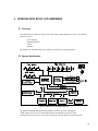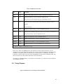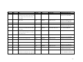
1
ADSP-21065L EZ-KIT Lite Evaluation System Manual Part Number: 82-000490-01 Revision 1.0 December 2000 Notice Analog Devices, Inc. reserves the right to make changes to or to discontinue any product or service identified in this publication without notice. Analog Devices assumes no liability for Analog Devices applications assistance, customer product design, customer software performance, or infringement of patents or services described herein. In addition, Analog Devices shall not be held liable for special, collateral, incidental or consequential damages in connection with or arising out of the furnishing, performance, or use of this product. Analog Devices products are not intended for use in life-support applications, devices, or systems. Use of an Analog Devices product in such applications without the written consent of the Analog Devices officer is prohibited. Users are restricted from copying, modifying, distributing, reverse engineering, and reverse assembling or reverse compiling the ADSP-21065L EZ-KIT Lite operational software (one copy may be made for back-up purposes only). No part of this document may be reproduced in any form without permission. Trademark and Service Mark Notice The Analog Devices logo, SHARC, the SHARC logo, VisualDSP, the VisualDSP logo, and EZ-ICE are registered trademarks; and TigerSHARC, the TigerSHARC logo, White Mountain DSP, VisualDSP++, the VisualDSP++ logo, Apex-ICE, EZ-KIT Lite, Mountain-ICE, Summit-ICE, Trek-ICE, and The DSP Collaborative are trademarks of Analog Devices, Inc. Microsoft and Windows are registered trademarks and Windows NT is a trademark of Microsoft Corporation. Adobe and Acrobat are trademarks of Adobe Systems Incorporated. All other brand and product names are trademarks or service marks of their respective owners. Limited Warranty The ADSP-21065L EZ-KIT Lite hardware is warranted against defects in materials and workmanship for a period of one year from the date of purchase from Analog Devices or from an authorized dealer. Copyright © 2000, Analog Devices, Inc. All rights reserved. Revision 1.0, December 2000 ii TABLE OF CONTENTS LIST OF TABLES ........................................................................................................................................ 5 LIST OF FIGURES ...................................................................................................................................... 6 1 INTRODUCTION................................................................................................................................. 7 1.1 1.2 1.3 1.4 1.5 1.6 2 FOR MORE INFORMATION ABOUT ANALOG DEVICES, INC. PRODUCTS............................................ 8 FOR TECHNICAL OR CUSTOMER SUPPORT........................................................................................ 8 PURPOSE OF THIS MANUAL.............................................................................................................. 8 INTENDED AUDIENCE....................................................................................................................... 8 MANUAL CONTENTS DESCRIPTION .................................................................................................. 9 DOCUMENTS AND RELATED PRODUCTS ......................................................................................... 10 GETTING STARTED ........................................................................................................................ 11 2.1 OVERVIEW ..................................................................................................................................... 11 2.2 CONTENTS OF YOUR EZ-KIT LITE PACKAGE ................................................................................ 11 2.3 PC CONFIGURATION ...................................................................................................................... 12 2.4 VISUALDSP++............................................................................................................................... 12 2.5 INSTALLATION PROCEDURES ......................................................................................................... 13 2.5.1 Installing the EZ-KIT Lite Hardware ........................................................................................ 13 2.5.2 Installing VisualDSP++ ............................................................................................................ 13 2.5.3 Installing the VisualDSP++ EZ-KIT Lite License .................................................................... 14 2.5.4 Installing the EZ-KIT Lite Software ......................................................................................... 14 3 USING EZ-KIT LITE SOFTWARE ................................................................................................. 16 3.1 OVERVIEW ..................................................................................................................................... 16 3.2 STANDARD OPERATION.................................................................................................................. 16 3.2.1 I/O Devices ............................................................................................................................... 16 3.2.2 POST Routines.......................................................................................................................... 19 3.2.3 Monitor Program Operation...................................................................................................... 21 3.2.4 AD1819 Transmissions............................................................................................................. 22 3.3 RUNNING YOUR OWN PROGRAMS ................................................................................................. 23 3.3.1 ADSP-21065L Memory Map.................................................................................................... 23 3.3.2 Using the AD1819A SoundPort Codec as the Analog Front End ............................................. 26 3.3.3 Method 1: Using the Monitor’s Codec DMA Buffers and Interrupt Handler ........................... 26 3.3.4 DSP Programming of the AD1819 Indexed Control Registers ................................................. 31 3.3.5 EMAFE Programming .............................................................................................................. 31 4 DEMONSTRATION PROGRAMS .................................................................................................. 32 4.1 OVERVIEW ..................................................................................................................................... 32 4.2 STARTING THE VISUALDSP++ DEBUGGER .................................................................................... 32 4.3 DEBUGGER OPERATION WITH THE ADSP-21065L EZ-KIT LITE ................................................... 33 4.3.1 Loading Programs ..................................................................................................................... 33 4.3.2 Registers and Memory .............................................................................................................. 34 4.3.3 Setting Breakpoints and Stepping ............................................................................................. 34 4.3.4 Resetting the EZ-KIT Lite Board.............................................................................................. 35 4.4 BENCHMARKING UTILITIES ............................................................................................................ 35 4.5 DEMONSTRATION PROGRAMS ........................................................................................................ 37 4.5.1 FFT.dxe..................................................................................................................................... 37 4.5.2 BP.dxe....................................................................................................................................... 37 4.5.3 Pluck.dxe................................................................................................................................... 37 4.5.4 Gunn.dxe................................................................................................................................... 37 3 4.5.5 Primes.dxe................................................................................................................................. 38 4.5.6 Tt.dxe ........................................................................................................................................ 38 4.5.7 Blink.dxe................................................................................................................................... 38 5 WORKING WITH EZ-KIT LITE HARDWARE............................................................................ 39 5.1 OVERVIEW ..................................................................................................................................... 39 5.2 SYSTEM ARCHITECTURE ................................................................................................................ 39 5.3 BOARD LAYOUT............................................................................................................................. 40 5.3.1 Boot EPROM............................................................................................................................ 40 5.3.2 User Push-Button Switches ....................................................................................................... 41 5.3.3 User LED’s ............................................................................................................................... 41 5.4 POWER SUPPLIES ........................................................................................................................... 41 5.4.1 Power Connector....................................................................................................................... 42 5.4.2 European Power Supply Specifications..................................................................................... 42 5.4.3 AD1819 Connections ................................................................................................................ 43 5.4.4 Expansion Port Connectors ....................................................................................................... 43 5.4.5 EMAFE Interface Connector .................................................................................................... 43 5.4.6 JTAG Connector (Emulator Port) ............................................................................................. 43 5.5 JUMPERS ........................................................................................................................................ 44 5.5.1 Boot Mode Selection Jumper .................................................................................................... 44 5.5.2 EPROM Size Selection Jumpers ............................................................................................... 45 5.5.3 Processor ID Jumpers................................................................................................................ 45 5.6 EPROM OPERATION ..................................................................................................................... 46 5.6.1 Designers Note.......................................................................................................................... 47 5.7 UART............................................................................................................................................ 47 5.7.1 Designers Note.......................................................................................................................... 47 5.8 EMAFE ......................................................................................................................................... 48 5.9 AD1819......................................................................................................................................... 48 5.10 S .................................................................................................................................................... 48 5.11 TIMING DIAGRAMS ........................................................................................................................ 49 6 EXPANSION CONNECTORS .......................................................................................................... 52 6.1 OVERVIEW ..................................................................................................................................... 52 6.2 EMAFE EXPANSION ...................................................................................................................... 53 6.2.1 EMAFE Connector Interface Signal Descriptions .................................................................... 56 7 REFERENCE...................................................................................................................................... 59 7.1 OVERVIEW ..................................................................................................................................... 59 7.2 SETTINGS MENU COMMANDS ........................................................................................................ 59 7.2.1 Test Communications................................................................................................................ 59 7.2.2 Baud Rate.................................................................................................................................. 59 7.2.3 Comm Port ................................................................................................................................ 60 7.2.4 Codec ........................................................................................................................................ 60 7.3 DEMO MENU COMMANDS.............................................................................................................. 61 APPENDIX A RESTRICTIONS & CPLD CODE LISTING ................................................................. 63 APPENDIX B BILL OF MATERIALS .................................................................................................... 72 APPENDIX C SCHEMATICS .................................................................................................................. 78 INDEX ......................................................................................................................................................... 79 4 LIST OF TABLES TABLE 2-1 TABLE 2-2 TABLE 3-1 TABLE 3-2 TABLE 3-3 TABLE 3-4 TABLE 3-5 TABLE 3-6 TABLE 3-7 TABLE 5-1 TABLE 5-2 TABLE 5-3 TABLE 5-4 TABLE 5-5 TABLE 5-6 TABLE 5-7 TABLE 5-8 TABLE 6-1 TABLE 6-2 TABLE 6-3 TABLE 6-4 TABLE 6-5 TABLE 6-6 TABLE 7-1 PC MINIMUM CONFIGURATION ................................................................................................... 12 USER CONFIGURABLE EZ-KIT LITE SETTINGS ........................................................................... 15 FLAG SUMMARY ......................................................................................................................... 17 INTERRUPTS USED BY THE MONITOR PROGRAM ......................................................................... 18 TABLE 3-3. POST ROUTINES........................................................................................................ 19 TABLE 3-4. POST ERROR CODES ............................................................................................... 19 MEMORY MAP ............................................................................................................................ 24 AVAILABLE MEMORY LOCATIONS ON THE EZ-KIT LITE ............................................................ 25 DSP PROGRAMMING OF THE AD1819 INDEXED CONTROL REGISTERS ....................................... 31 POWER CONNECTOR ................................................................................................................... 42 EUROPEAN POWER SUPPLY SPECIFICATIONS ............................................................................... 42 BOOT MODE SELECTION ............................................................................................................. 44 EPROM SIZE SELECTION ........................................................................................................... 45 PROCESSOR SELECTION .............................................................................................................. 45 LINE IN SELECTION ..................................................................................................................... 46 AD1819 CODEC SELECTION ....................................................................................................... 46 SDRAM PIN CONNECTIONS ........................................................................................................ 49 EXPANSION CONNECTORS ........................................................................................................... 52 EVALUATION BOARD POWER CONNECTIONS .............................................................................. 54 EMAFE CONNECTOR ................................................................................................................. 55 EMAFE CONNECTOR INTERFACE SIGNAL DESCRIPTION ROW A ................................................ 56 EMAFE CONNECTOR INTERFACE SIGNAL DESCRIPTION ROW B ................................................ 57 EMAFE CONNECTOR INTERFACE SIGNAL DESCRIPTION ROW C ................................................ 58 FFT DEMO DIALOG DESCRIPTION............................................................................................... 61 5 LIST OF FIGURES FIGURE 3-1 ADSP-21065L EZ-KIT LITE MONITOR KERNEL CODEC TRANSFER SCHEME ............................ 28 FIGURE 4-1 TARGET SELECTION DIALOG ....................................................................................................... 32 FIGURE 4-2 TARGET MESSAGE ...................................................................................................................... 33 FIGURE 4-3 TARGET COMMUNICATIONS STATUS MESSAGE BOX .................................................................. 33 FIGURE 5-1 EZ-KIT LITE SYSTEM BLOCK DIAGRAM .................................................................................... 39 FIGURE 5-2 EZ-KIT LITE LAYOUT............................................................................................................... 40 FIGURE 5-3 JTAG CONNECTOR WITH JUMPERS INSTALLED.......................................................................... 44 FIGURE 5-4 EPROM ADDRESS (256K X 8 EXAMPLE) ................................................................................... 47 FIGURE 5-5 EMAFE WRITE CYCLE TIMING PARAMETER DEFINITIONS ......................................................... 49 FIGURE 5-6 EMAFE WRITE CYCLE TIMING DIAGRAM .................................................................................. 50 FIGURE 5-7 EMAFE READ CYCLE TIMING PARAMETER DEFINITIONS .......................................................... 50 FIGURE 5-8 EMAFE READ CYCLE TIMING DIAGRAM ................................................................................... 51 FIGURE 6-1 PHYSICAL LAYOUT OF ADSP-21065L DSP EVALUATION BOARD AND EMAFE DAUGHTER BOARD ................................................................................................................................................... 54 FIGURE 7-1 SETTINGS MENU COMMANDS ..................................................................................................... 59 FIGURE 7-2 SAMPLE RATE DIALOG ................................................................................................................ 60 FIGURE 7-3 SOURCE SETTING ........................................................................................................................ 60 FIGURE 7-4 FFT DEMO DIALOG .................................................................................................................... 61 FIGURE 7-5 BANDPASS DEMO CONTROLS DIALOG ........................................................................................ 62 6 1 INTRODUCTION Thank you for purchasing the ADSP-21065L EZ-KIT Lite evaluation kit. The evaluation board is designed to be used in conjunction with VisualDSP++ development environment and is based on the ADSP-21065L SHARC® floating-point digital signal processor (DSP). The kit is shipped with an evaluation board and VisualDSP++ software. The VisualDSP++ that comes with the kit will only operate with the evaluation board. The complete version must be purchased seperately. Using the EZ-KIT Lite with VisualDSP++, you can observe the ADSP-21065L DSP execute programs from onchip RAM, interact with on-board devices, and communicate with other peripherals. You can access the ADSP-21065L SHARC processor using the PC through a serial port or an optional JTAG emulator. The monitor program that runs on the EZ-KIT Lite, gives you access to the ADSP21065L processor’s internal memory space through the serial port. In contrast, the JTAG emulator allows the PC to perform in-circuit emulation through the processor’s JTAG interface. The board’s features include: • Analog Devices ADSP-21065L DSP running at 60MHz • Analog Devices AD1819A 16-bit SoundPort® Codec • RS-232 interface • Socketed EPROM (128K x 8 on board, or 256K x 8, 512K x 8, and 1M x 8 selectable) • SDRAM (1M x 32) • Four push buttons for Flag inputs • Three push buttons for IRQ inputs • Six user programmable LEDs • Power supply regulation • EMAFE (Enhanced Modular Analog Front End) connector for expansion • Expansion connectors The EZ-KIT Lite board is equipped with hardware that facilitates interactive demonstrations. The push button switches and user programmable LEDs provide user control and board status. Additionally, the AD1819A SoundPort Codec provides access to an audio input (selectable as line level or microphone) and an audio output (line level). The EZ-KIT Lite includes a monitor program stored in non-votilitile memory. The monitor program allows the user to download, execute and debug ADSP-21065L programs. By removing the socketed EPROM, replacing it with an EPROM containing user code, the board can run as a stand-alone unit, without the PC. 7 The user can also connect a JTAG emulator to the EZ-KIT Lite. Through the JTAG emulator, you can load programs, start and stop program execution, observe and alter registers and memory, and perform other debugging operations. JTAG emulators are purchased seperately through Analog Devices. Additionally, the EZ-KIT Lite provides expansion connectors that let the user examine the processor signals, as well as provide an interface for host control. 1.1 For More Information About Analog Devices, Inc. Products Analog Devices is accessible on the Internet at www.analog.com. The DSP web page is directly accessible at www.analog.com/dsp. This page provides access to DSP specific technical information and documentation, product overviews, and product announcements. 1.2 For Technical or Customer Support You can reach our Customer Support group in the following ways: • Email questions to [email protected] • Contact your local Analog Devices sales office or an authorized Analog Devices distributor 1.3 Purpose of This Manual The ADSP-21065L EZ-KIT Lite evaluation system manual gives directions for installing the evaluation board and software on the PC. Also, the manual provides guidelines for running user code on the ADSP-21065L. 1.4 Intended Audience This manual is a user’s guide and reference to the ADSP-21065L EZ-KIT Lite evaluation board. DSP programmers who are familiar with Analog Devices SHARC architecture, operation, and programming are the primary audience for this manual. DSP programmers who are unfamiliar with Analog Devices DSPs can use this manual, but should supplement this manual with the ADSP-21065L User’s Manual, the ADSP-21065L Technical Reference and the VisualDSP++ tools manuals. 8 1.5 Manual Contents Description This manual contains the following information: • Chapter 1 — Introduction Provides manual information and Analog Devices contact information. • Chapter 2 — Getting Started Provides software and hardware installation procedures, PC system requirements, and basic board information. • Chapter 3 — Using EZ-KIT Lite Software Provides information on the EZ-KIT Lite system from a software perspective, and details the monitor program, EMAFE, and codec. • Chapter 4 — Demonstration Programs Provides information on VisualDSP++ debugger operation with the ADSP-21065L EZ-KIT Lite, benchmarking utilities, and demonstration programs. • Chapter 5 — Working With EZ-KIT Lite Hardware Provides information on the Hardware aspects of the evaluation system. • Chapter 6 — Expansion Connectors Provides information on EMAFE expansion and descriptions of connector interface signals. • Chapter 7 — Reference Provides information on settings menu commands and demo menu commands. • Appendix A — Restrictions & CPLD Code Listing Provides information on board restrictions you may encounter when using your EZ-KIT Lite, and the files used on the programmable device(s) on the EZ-KIT Lite board. • Appendix B — Bill of Materials Provides a list of components used in the manufacture of the EZ-KIT Lite board. Appendix C — Schematics Provides a resource to allow EZ-KIT Lite board level debugging or to use as a reference design. 9 1.6 Documents and Related Products For more information on the ADSP-21065L and the components of the EZ-KIT Lite system, see the following documents: • ADSP-21065L SHARC User's Manual & Technical Reference • ADSP-21065L • AC’97 SoundPort® The ADSP-2106x family of processors is supported by a complete set of evaluation tools. Software tools include a C compiler, assembler, runtime libraries and librarian, linker, simulator, and PROM splitter. See the following documents: • VisualDSP++ Getting Started Guide • VisualDSP++ User's Guide for the ADSP-21xxx Family DSPs • Assembler Manual for the ADSP-21xxx Family DSPs • C/C++ Compiler & Library Manual for the ADSP-21xxx Family DSPs • Linker & Utilities for the ADSP-21xxx Family DSPs • Product Bulletin for VisualDSP++ and the ADSP-21xxx Family DSPs These documents are found on the Analog Devices Technical Documentation web site at http://www.analog.com/industry/dsp/tech_doc/gen_purpose.html#32 If you plan to use the EZ-KIT Lite in conjunction with the JTAG emulator, refer to the documentation that accompanies the emulator. Your software installation kit includes on-line help as part of the Windows interface. These help files provide information about the ADSP-21065L evaluation board and accompanying tools. 10 2 GETTING STARTED 2.1 Overview This chapter provides information to install the software and the ADSP-21065L evaluation board. It is important that installation of the software and hardware are in the order presented for correct operation. This chapter also provides basic board information and conatins the following sections: • Contents of your EZ-KIT Lite package • PC configuration • Installation procedures 2.2 Contents of Your EZ-KIT Lite Package The EZ-KIT Lite evaluation board contains ESD (electrostatic discharge) sensitive devices. Electrostatic charges readily accumulate on the human body and equipment and can discharge without detection. Permanent damage may occur on devices subjected to high energy discharges. Proper ESD precautions are recommended to avoid performance degradation or loss of functionality. Unused EZ-KIT Lites should be stored in the protective shipping package. The ADSP-21065L EZ-KIT Lite evaluation board package should contain the following items. If any item is missing, contact the vendor where you purchased your EZ-KIT Lite or Analog Devices. • ADSP-21065L EZ-KIT Lite board • Power cable with DC power supply (7.5 Volts) • RS-232 serial port 9-pin cable • EZ-KIT Lite CD containing examples, target .dll files, help files, and utilities • VisualDSP++ CD • Registration card - please fill out and return 11 2.3 PC Configuration For correct operation of the VisualDSP++ software and EZ-KIT Lite demos, all computers must have the minimum configuration shown below. Table 2-1 PC Minimum Configuration Windows 95, 98, 2000 Windows NT Windows 95 OSR2, Windows 98, or Windows 2000 Windows NT, release 4.0, Service Pack 3 or later Pentium processor 166 MHz or faster Pentium processor 166 MHz or faster VGA Monitor and color video card VGA Monitor and color video card 2-button mouse 2-button mouse 100 MB available space 100 MB available space 32 MB RAM 32 MB RAM CD-ROM CD-ROM 2.4 VisualDSP++ The ADSP-21065L EZ-KIT Lite system is shipped with the VisualDSP++ Integrated Development Environment (IDE), debugger and code generation tools. VisualDSP++ is limited in functionality by the EZ-KIT Lite serial number that is shipped with this product. The EZ-KIT Lite serial number restricts the VisualDSP++ debugger to only connect to the ADSP-21065L EZKIT Lite evaluation board running the debug monitor via the serial port (no emulator or simulator support). Additionally, the linker will restrict the user to only 25% (2.5k words) of the ADSP21065L’s on-chip program memory space. If the full VisualDSP++ software suite is purchased, the user will obtain a new serial number from Analog Devices that will lift the restrictions mentioned above. The basic components that are shipped with VisualDSP++ are: • Integrated Development Environment (IDE) — graphical interface for project management, allowing the user to set project options, access the code generation tools, and launch the debugger. • Debugger — allows the user to view the insides of the DSP and perform debug operations such as read/write memory, read/write registers, load programs, run, step, halt, and more. • SHARC Family Code Generation Tools — C compiler, assembler, runtime libraries and librarian, linker, simulator, and PROM splitter. • Example Projects — Both VisualDSP++ and the ADSP-21065L EZ-KIT Lite are shipped with example projects and C and Assembly source code that demonstrate various features of the tools and ADSP-21065L DSP. 12 2.5 Installation Procedures The following procedures are provided for the safe and effective use of the ADSP-21065L evaluation board. It is important that you follow these instructions in the order presented to ensure correct operation of your software and hardware. 2.5.1 Installing the EZ-KIT Lite Hardware The ADSP-21065L EZ-KIT Lite board is designed to run outside the PC as a stand alone unit. There is no need to remove the chassis from your computer. Use the following steps to connect the EZ-KIT Lite board: 1. Remove the EZ-KIT Lite board from the package—be careful when handling these boards to avoid the discharge of static electricity, which may damage some components. 2. Connect the RS-232 cable to an available Comm Port on the PC and to J3 on the ADSP-21065L evaluation board. 3. Plug the provided cord into a 120-Volt AC receptacle and plug the connector at the other end of the cable into J1 (Power In) on the evaluation board. All of the LEDs light up briefly. The FLAG9 and power (red) LED remain on. If the LEDs do not light up, check the power connections. To configure your board to take advantage of the audio capabilities of the demos, use the following procedure: 1. Plug a set of self-powered computer speakers into jack J7(Line Out) on the board. Turn on the speakers and set the volume to an adequate level. 2. Connect the line out of an electronic audio device to jack J8 (MIC/Line In) on the board. Set jumpers JP1 and JP2 to LINE. 3. Set Jumper JP3 to GND to enable the AD1819 codec. (This is the board default) This completes the hardware installation. 2.5.2 Installing VisualDSP++ This EZ-KIT Lite comes with the latest evaluation version of VisualDSP++ for SHARC Family DSPs. You must install this software prior to installing the EZ-KIT Lite software. Insert the VisualDSP++ CD into the CD-ROM drive. This will bring up the CD browser. Click on the “Install VisualDSP++” option. This will launch the setup wizard. Follow this wizard with the on-screen instructions. 13 2.5.3 Installing the VisualDSP++ EZ-KIT Lite License Before the VisualDSP++ software can be used, the license must be installed. To install the EZ-KIT Lite license, follow these steps: 1. Make sure VisualDSP++ has been installed first. 2. Insert the VisualDSP++ CD into the CD-ROM drive if it is not already in the drive. 3. Once the CD browser is on the screen select the "Install License" option. 4. Now follow the setup wizard instructions. (Note: Make sure that you have the proper serial number located on the back of the CD holder.) 2.5.4 Installing the EZ-KIT Lite Software The EZ-KIT Lite software is supplied on a separate CD-ROM. To install the EZ-KIT Lite software, follow these steps: 1. Make sure VisualDSP++ has been installed first. 2. Close all Windows applications. The install will not work correctly if any VisualDSP++ applications are running. 3. Insert the EZ-KIT Lite CD into the CD-ROM drive. The setup will automatically start. Follow the installation wizard by choosing the appropriate options. 4. When the setup has completed reboot the machine, if necessary. 14 2.5.4.1 Default Settings After you have installed the board and utility software, your PC and EZ-KIT Lite have the default settings shown in Table 2-2. You can change these settings through the Settings menu in the debugger. Table 2-2 User Configurable EZ-KIT Lite Settings Selection Default Setting Comm Port Comm 1 Baud Rate 115200 Codec Sample Rate 48000 Hz Codec Source Microphone Codec Gain 0.0 2.5.4.2 On-Line Help The VisualDSP++ Debugger comes with a complete on-line help file and Adobe .pdf files of all manuals. • You can use the context help button to get help on any command or icon or • Highlight a command and press F1. For help on commands and dialogs click from the toolbar Help -> Help Topics to get to the Debugger Help help file. 15 3 USING EZ-KIT LITE SOFTWARE 3.1 Overview The combination of the EZ-KIT Lite board and the monitor software operate as a target for the VisualDSP++ debugger. The debugger allows viewing of the processor registers and memory, perform several debugging activities, such as: setting breakpoints, stepping through code, and plotting a range of memory. If VisualDSP++ is not installed, please install it from the VisualDSP++ CD that came with this product. For more information, refer to Chapter 2, section “VisualDSP++”. This chapter provides monitor level software information on how the EZ-KIT Lite board operates with the installed software. This chapter also provides information that helps the user run his/her own programs on the ADSP-21065L EZ-KIT Lite board. This information appears in the following sections: • “Standard Operation” Describes the operation of the EZ-KIT Lite board, from Power On self Test (POST) routines to the AD1819 codec’s operation. • “Running Your Own Programs” Provides information about writing and running your own DSP executables that link with the monitor program to run on the EZ-KIT Lite board. 3.2 Standard Operation This section covers the standard operation of the EZ-KIT Lite board. It describes the I/O capabilities of the on-board components, board power-up, and the on-board Monitor program. 3.2.1 I/O Devices 3.2.1.1 Flags The ADSP-21065L has 12 asynchronous FLAG I/O pins that let you interact with the running program. All flags are configured as inputs on reset of the DSP. For more information on the Flag pins, see Chapter 12, “System Design, Flag Pins” in the ADSP21065L SHARC User’s Manual. The flags and their uses, are as follows: • FLAG0-3 are connected to the push buttons on the EZ-KIT Lite board and are for user input. For instance, the user can tell the program to poll for a flag and when it occurs, do some other operation such as jump to another instruction. The push button flags are set as inputs through the MODE2 register. Once configured, they may be read through the ASTAT register. 16 • FLAG4-9 connect to the LEDs and supply feedback for program execution. For example the user can write code to trigger a flag (and the corresponding LED) when a routine is complete the LED will light. The LED flags are configured through the IOCTL register and are set/read through the IOSTAT register. • FLAG10 is available to the EMAFE interface and is used for signaling. The EMAFE flag is configured through the IOCTL register and is set/read through the IOSTAT register. • FLAG11 is reserved for the monitor to determine if the AD1819 codec is enabled. When using the monitor program supplied with the EZ-KIT Lite board, do not use or alter this flag pin. Table 3-1 Flag Summary Flag Use Flag0-3 Push-button Input (SW3, SW5, SW7, SW8) Flag4-9 LED Feedback Flag10 EMAFE Flag Flag11 Reserved for monitor 3.2.1.2 Interrupts Each of the three external interrupts, IRQ0-2, of the ADSP-21065L are directly accessible through push button switches SW2, SW4, and SW6 on the EZ-KIT Lite board. IRQ0-1 are “wire-Or’ed”; IRQ0 is used to implement interrupt driven serial routines with the UART and IRQ1 is provided for use with an EMAFE board and can be set to read and write registers. The external interrupts are controlled through the MODE1, MODE2, and IMASK registers and are configured in one of two ways: by modifying the vector table or through instructions in user code. The MODE2 register also controls the interrupt sensitivity between level and edge. To prevent an interrupt from being masked, write to the particular interrupt in the IMASK register. The monitor program running on the ADSP-21065L uses three interrupts; IRQ0, SPT1I and SFT3, for normal operation. These interrupt vectors are provided in the “demorth.asm” file that comes with the EZ-KIT Lite. 17 When writing code, these interrupts (and their corresponding vectors) should not be altered. If these vectors are overwritten, the kernel may not work as shown in Table 3-1. For more information on the registers that control interrupts, and a complete list of interrupt vector addresses, see Appendix E and F in the ADSP-21065L SHARC Technical Reference. Table 3-2 Interrupts Used by the Monitor Program Interrupt Description Lost Functionality if Overwritten IRQ0 Multiplexed from the UART through Debugger’s ability to interrupt an open collector device running code SFT3 Used to signal the monitor to send Ability to send messages from data back to the Host SPT1 user code to the debugger AD1819 Transmit Interrupt Monitor’s ability to control the AD1819 SPR1 AD1819 Receive Interrupt The following rules and restrictions should be followed when using interrupts: • You cannot step into an interrupt. • Interrupts are disabled when the user program is halted. • The board cannot communicate with the host if an interrupt higher than IRQ0 is used. • The board cannot communicate with the host if interrupt nesting is disabled. • If the user does not require the supplied monitor program, IRQ0 with SW2 can be configured by the user. In the initialization code of the user’s program, the interrupt vector for IRQ0 must be replaced. This removes all monitor functionality. • If the user does not connect an EMAFE to the EZ-KIT Lite, IRQ1 with SW4 can be configured for other purposes. If an EMAFE card is attached and it uses IRQ1, there is no way to disable the EMAFE's control of the interrupt line. If the EMAFE is not attached, IRQ1 is available for other uses. Note: the monitor program does not interact with the EMAFE board, and does not have any response to an IRQ1 request. 3.2.1.3 Serial Ports The ADSP-21065L features two synchronous Serial Ports (SPORT0 and SPORT1). The SPORTs can operate at up to 1x clock frequency, providing each with a maximum data rate of 30 Mbit/sec. Each SPORT has a primary and a secondary set of transmit and receive channels. SPORT data can be automatically transferred to and from on-chip memory using DMA. 18 Each of the SPORTs supports three operation modes: DSP SPORT mode, I2S mode (an interface commonly used by audio codecs) and TDM (Time Division Multiplex) multichannel mode. For additional information on the serial ports please refer to Chapter 9 of the ADSP-21065L SHARC User’s Manual. Both of the synchronous serial ports are connected to the EMAFE interface. SPORT1 is also connected to the on-board AD1819. Jumper JP3 is used to disable the AD1819, so it doesn’t interfere with the EMAFE. For normal operation of the AD1819, JP3 must be connected to GND. If the EMAFE is using SPORT1, the serial communication to the AD1819A should be disabled by connecting JP3 to +3.3VCC. 3.2.2 POST Routines POST (Power On Self Test) routines are a series of standard tests and initializations that the EZ-KIT Lite performs on a power-on reset. To perform a power-on reset, disconnect power to the board for at least three seconds and then reconnect power. The board automatically resets (note that all the LED’s light up briefly). The user may also reset the board during operation through the Debug -> Reset command from the debugger menu bar. Both types of reset cause the DSP to reset to a known state and is followed by a message box that displays the message “Communications Success”. At this point the user should reload any programs he/she was working on. Table 3-3 shows the types of resets and their functions. Table 3-3 Table 3-3. Post Routines Routine EPROM Check Internal Memory Check External Memory Check UART Check AD1819 Check Initializations Power-on Reset Yes Yes Yes Yes Yes Yes Reset During Operation No No No No No Yes Error codes are transmitted to the PC and are displayed on the LEDs. If the LED remains lit after reset, then the error has been caused by the component shown in Table 3-4 Table 3-4 Table 3-4. POST Error Codes Flag LED 4 5 6 7 Error EPROM UART AD1819 Memory 19 3.2.2.1 Memory Checks The monitor program performs some standard memory checks which are as follows: • EPROM • Internal memory • External SDRAM The EPROM test consists of verifying a number in memory. If the monitor code is corrupted, the monitor may crash before reaching the actual program code. These checks include: • Write, then verify all 0’s • Write, then verify all 1’s • Write, then verify memory address • Write, then verify compliment of memory address 3.2.2.2 UART Check/Initialization The UART check is done in three stages. Two of these stages are implemented in the POST. The third is controlled by the host (PC), when it attempts to connect to the EZ-KIT Lite. These stages are: • Register Write This test confirms that the ADSP-21065L is capable of writing to and reading from a register in the UART. Three patterns are written to and then read from a register in the UART, and tested. All three patterns must be read back correctly to pass this test. • Internal Loop Back In this test, 256 bytes are sent to and read from the UART. This test checks the functionality of the UART connections from the ADSP-21065L, up to and through the UART chip. • Transmitted Loop Back The last UART test is performed by the host after the POST is complete. In this test, the host sends the UART test protocol. This protocol specifies the number of bytes that are transmitted to the EZ-KIT Lite board, and instructs the board to echo the byte stream back to the host. This test determines whether the EZ-KIT Lite board is set to the correct baud rate, and verifies the external connections between the board and the host. 20 On power up, the EZ-KIT Lite board defaults to a baud rate of 115200 baud with 8 data bits, 1 stop bit, and no parity. If you want to change this rate change it after the POST is complete use the Settings -> Baud Rate command from the debugger menu bar. Note that setting the baud rate to a lower number can significantly slow the boards response to all debug activities. 3.2.2.3 AD1819 Check/Initialization On reset, the AD1819 begins transmitting the clock used to synchronize data transfers over SPORT1. Once this bit goes high, the AD1819 is ready for standard communication over SPORT1. The POST then writes and verifies three patterns to an internal register in the AD1819. If all three writes are verified, the connection is verified. 3.2.3 Monitor Program Operation The monitor program runs on the EZ-KIT Lite board as part of the DSP executable and provides the ability to download, debug, and run user programs. The VisualDSP++ debugger is the interface for the monitor and using the EZ-KIT Lite as a target with the debugger lets you operate the board remotely. There are three main components of the monitor program: • Halt loop • UART ISR • Command Processing Kernel The monitor program idles in the Halt loop when it is not running user code. While there, you can read/write memory, read/write registers, download programs, set breakpoints, change the UART’s baud rate, modify the AD1819 configuration, and single step through code. To enter the halt loop from your code, you must halt user code—either with a breakpoint or a halt instruction. At this point, the halt loop polls the UART. With every character received from the UART, the command processing kernel verifies whether a full command has been received. If a command has been received, the kernel processes the command; otherwise control is returned to the halt loop to wait for more characters. The only method of executing your code once the halt loop has been entered is to send a Run or Single Step command in the debugger. The UART ISR is entered when user code is running, but the host is still interacting with the board. As the host sends bytes, the UART ISR takes the data stream from the UART, and builds the command. As with the halt loop, each character received is passed to the command processing kernel. Unlike the halt loop, the monitor returns to the user code immediately after the interrupt is serviced. 21 The following restrictions should be followed to ensure correct board operation. • The host loses contact with the monitor while the user program is running if the user program disables the UART interrupt or changes the UART interrupt vector. • The host loses contact with the monitor while the program is running and in an ISR when nesting is turned off. • The host loses contact with the monitor while the program is running and in the timer ISR, provided the highest priority timer vector is used. • The host cannot halt with the debugger’s Debug, Halt command if global IRQ enable is disabled (IRPTEN bit), however, breakpoints will work. Command processing, initiated from either the UART ISR or the Halt Loop, is done in the command processing kernel. This kernel parses the commands and executes the instructions. If the instruction requires data to be sent back to the host, the kernel initiates the response. 3.2.3.1 Break Points The ability to stop the execution of code and examine processor registers and memory is extremely helpful when debugging code. Note that the debugger automatically inserts breakpoints an the function Main(), when the Settings -> Run To Main command is checked, and at the _exit instruction. 3.2.4 AD1819 Transmissions After reset, the AD1819 generates the clock used to transfer data across SPORT1. The ADSP-21065L initiates all transmissions with the AD1819 by sending a synchronization pulse. Even though the AD1819 transmits the data clock, it may not be ready for normal operation. Until the AD1819 is ready, it holds the first bit (AD1819 Ready bit) of SLOT 0 low. When ready, this bit is driven high. The first transmission to the AD1819 is done differently than subsequent transmissions. The packets initially expected by the AD1819 do not have a consistent size. This first transmission instructs the AD1819 to standardize the packet size to 16-bit. This command is created by shifting and stuffing bits in the transmit buffer. Slot 0 in each transmission specifies which slots contain valid data. The ADSP-21065L uses DMA transfers to automatically send and receive data from the AD1819. When the transmit DMA empties the transmit buffer, an interrupt occurs. If Tx Request > 0, the interrupt loads the data from the User Tx buffer into the Tx buffer. If the variable Tx Request < 0 the Tx buffer is loaded with 0s. After the Tx buffer is loaded, the DMA is initialized to transmit the new data in the Tx buffer. The receive portion of the AD1819 interface is designed in a similar way. The DMA for SPORT1’s receive register is configured to load the Rx buffer. 22 When the Rx buffer is full, an interrupt is generated that checks the Rx request variable. If the variable > 0 then the contents of the Rx buffer are written into the User Rx Buffer, and the Rx request is cleared. Afterwards, the DMA is re-initialized to fill the Rx buffer again. 3.3 Running Your Own Programs This section provides the user with the basic information that is needed to run their own programs on the ADSP-21065L EZ-KIT Lite. Build these programs using the SHARC tools. This information includes rules for using processor memory, a description AD1819 control registers (with respect to DSP programming), and a simple program generation procedure. Although there are many ways to go about developing programs in the VisualDSP++ environment, all program evaluation within the environment should include the following steps: • Step1: Create a New Project File • Step 2: Set Target Processor Project Options • Step 3: Add and Edit Project Source Files • Step 4: Customize Project Build Options • Step 5: Build a Debug Version of the Project • Step 6: Debug the Project • Step 7: Build a Release Version of the Project By following these steps, DSP projects build consistently and accurately with minimal project management. The ADSP-21065L SHARC Technical Reference and ADSP-21065L SHARC User’s Manual provides detailed information on programming the processor and the VisualDSP++ manuals provide information on code evaluation with the SHARC tools. • Do not run more than one ADSP-21065L EZ-KIT Lite Session in the debugger at any one time. You may run an EZ-KIT Lite session and a simulator or ICE session at the same time or you can open two debugger interfaces to run more than one EZ-KIT Lite session. • Before making changes to the source code in the IDE, the user needs to clear all breakpoints and close the source window. Then make the changes, rebuild the program and reload it into the debugger. 3.3.1 ADSP-21065L Memory Map The ADSP-21065L EZ-KIT Lite board contains 1M x 32 of external SDRAM. This memory is connected to MS3 (Memory Select). The ADSP-21065L has 544 Kbits of internal SRAM that can be used for either program or data storage. The configuration of on-chip SRAM is detailed in the ADSP-21065L SHARC User’s Manual. Table 3-5 shows the memory map of the ADSP-21065L EZ-KIT Lite. The IMDW0 bit in the SYSCON register must be set to 1 to keep communication with the host. This bit determines if data accesses made to internal memory block 0 are 40-bit three column accesses (set = 1) or 32-bit two column accesses (cleared = 0). The monitor program requires three column data accesses to memory block 0. 23 On reset, restart, and halt, the debug monitor kernal forces IMDW0 to 1 and IMDW1 to 0 but user code should also set these bits to ensure that it operates in the same way on both the simulator and the EZ-KIT Lite board. These settings only affect data accesses, not instruction fetches. • Block 0 resides in Three Column memory. If you are storing data in Block 0, it must be in three column format. • The user may not use DAG2 (PM data bus) to access SDRAM because SDRAM is mapped into an address that is greater than 24 bits. For example, the C segment seg_pmda should not be mapped to SDRAM. • If the user is using C interrupt handlers in his/her program, (i.e. interrupt()) then seg_dmda must not be located in external SDRAM. In this case seg_dmda MUST be located in internal memory. This is caused by a problem with the interrupt handlers in libc.dlb. A correction will be posted to the Analog Devices FTP site. Table 3-5 Memory Map Start Address End Address Content 0x0000 0000 0x0000 02FF Registers 0x0000 8000 0x0000 9FFF Block 0 Normal Address (internal memory) 0x0000 C000 0x0000 DFFF Block 1 Normal Address (internal memory) 0x0001 0000 0x0001 3FFF Block 0 Short word 0x0001 8000 0x0001 BFFF 0x0002 0000 0x0002 FFFF Block 1 Short word EPROM (through BMS)1 0x0100 0000 0x0100 0000 EMAFE Address (reserved for the EZ-KIT) 0x0100 0001 0x0100 0001 EMAFE Data (reserved for the EZ-KIT) 0x0100 0004 0x0100 0007 UART (reserved for the EZKIT) 0x0300 0000 0x0310 0000 SDRAM (reserved for the EZKIT) 1. Use caution when accessing the Boot EPROM. The EPROM chip select, BMS, has the same limitations as MS0. EPROMs larger than 128K x 8 have restricted access to their data below address 0x020000 and their data is aliased to other memory locations. The user program can access this data from these other locations. 24 Table 3-6 shows currently used and available memory locations on the EZ-KIT Lite board. The user may not change these locations in their programs. Table 3-6 Available Memory Locations on the EZ-KIT Lite Memory Range Availability 0x00008000 - 0x0000801F Interrupt Vectors - user (48-bit) 0x00008020 - 0x00008023 IRQ0 vector (reserved by monitor and not overwritten on any .dxe load) 0x00008024 - 0x00008033 Interrupt Vectors - user (48-bit) 0x00008034 - 0x00008037 SPORT Vector (reserved by monitor) 0x00008038 - 0x0000807B Interrupt Vectors - user (48-bit) 0x0000807C - 0x0000807F SWI3 Vector (reserved by monitor) 0x00008100 - 0x00008FFF User Program Space (3840 48-bit locations, internal RAM block 0) 0x00009000 - 0x000097FF 0x0000C000 - 0x0000DFFF Kernel Code (48-bit, internal block 0) User space (can be configured as 8192 x 32, or 2K x 48 + 4K x 32 or 4K x 48 +2K x 32) 0x01000000 EMAFE address location (external block 0) 0x01000001 EMAFE data location (external block 0) 0x01000008 - 0x0100000F 16550 UART registers (external block 0) 0x01000010 AD1819 reset address (external block 0) 0x03000000 - 0x030FFEFF User space (external block 3; 1048320 32-bit locations in SDRAM) 0x030FFF00 - 0x030FFF05 User AD1819 transmit buffer 0x030FFF06 User AD1819 transmit ready flag 0x030FFF07 - 0x030FFF0C User AD1819 receive buffer 0x030FFF0D User AD1819 receive ready flag 0x030FFF0E User SWI3 data pointer 0x030FFF0F User SWI3 number of data items 0x030FFF10 User SWI3 data type 0x030FFF11 - 0x030FFFFF Reserved for Kernel 25 3.3.2 Using the AD1819A SoundPort Codec as the Analog Front End There are two ways you can use the AD1819 SoundPort codec on the 21065L EZ-KIT Lite with the VisualDSP++ debugger. Method 1 — Use the codec DMA buffers and the codec interrupt handler within the EPROM monitor that are installed by the AD1819/SPORT1 initialization routine in the EPROM Monitor Program. This method is useful if you want to quickly test your DSP algorithm. This method may be preferable for early DSP evaluation, and the user does not need to be concerned with many of the details of the AD1819 theory of operation. The following section provides coding guidelines for the programmer to link in the required codec and SPORT DMA buffers. All of the audio demos provided with the ADSP-21065L EZ-KIT Lite use this method for communicating with the codec for RS-232 host codec control. Method 2 — Disabling and Overwriting the SPORT1 DMA codec buffers, and downloading a custom AD1819/SPORT1 initialization routine with the RS-232 monitor. The custom user routine includes instructions necessary to reset the codec, program SPORT1, activates serial port 1 transmit and receive DMA transfers, and programs any AD1819a register to a desired configuration. This method may be preferable if you want to test AD1819 code that may be downloaded via the SHARC JTAG, burnt into a new EPROM, or to test AD1819 functionality in a new custom-based 21065L design. For detailed AD1819 and SHARC interface information and example source that demonstrates this second method, contact Analog Devices DSP hotline or search our web site for the following document: Interfacing The ADSP-21065L SHARC DSP to the AD1819a 'AC97' SoundPort codec. Further information on the AC-97 serial protocol may be found in the AD1819A Datasheet. 3.3.3 Method 1: Using the Monitor’s Codec DMA Buffers and Interrupt Handler This section provides more detail on Method 1 from the previous section. The ADSP21065L uses DMA transfers to automatically send and receive data from the codec. After codec reset, the codec begins transmitting the clock used to synchronously transfer data across SPORT1. The ADSP-21065L, in turn, initiates all transmissions with the codec by sending a frame synchronization pulse. Even though the codec transmits the data clock, it may not be ready for normal operation. While the codec is not ready it holds the first bit (codec Ready bit) of SLOT 0 low. When ready, this bit is driven high. Once this bit goes high, the codec is ready for standard communication with the ADSP-21065L. The AD1819 initially expects all data transfers to be in packets according the AC'97 specification, where there is 1 x 16-bit time slot and 12 x 20 bit slots in the TDM audio frame. This packet scheme does not work well in DMA transfer schemes, nor to standard Multichannel Mode data transfers with the ADSP-21065L, which expects all slots to be the same number of bits. To realign your data, set the SLOT16 bit in the AD1819’s Serial Configuration register as soon the serial port is enabled. To do this, the program must perform a single transfer using the initial packing style. 26 After the SLOT16 bit is set, all subsequent packets are standardized to 16 bits. Once the data is aligned, the EPROM's monitor POST routine then writes and verifies three patterns to an internal register in the codec. If all three writes are verified, the codec connection is verified. The ADSP-21065L then continually transmits and receives data from the codec. Slot 0 in each transmission specifies which slots contain valid data (and are called the Tag Phase time slot). 3.3.3.1 Linking Your Code to the RS-232 Monitor Codec Interrupt Handlers To use the EPROM monitor’s interrupt handler for the AD1819, the user needs to use one of the following methods: C-code—link your code with the file demorth.asm (this is located in the ...\demos\tt folder). This file contains a replacement for the standard C runtime header 060_hdr.asm. This file also includes a jump to the EPROM codec interrupt handler at the SPORT1 Tx interrupt vector location. Assembly—use the demorth.asm file as the interrupt vector table or create your own interrupt vector table that includes a jump to address 0x9001at the SPORT1 Tx interrupt vector location. 3.3.3.2 Linking Your Code to the RS-232 Monitor DMA Buffers The monitor constantly sends and receives packets from the codec. To send data to the codec, the user needs to put the desired data into the codec transmit buffer, and set the transmit variable. Similarly, to receive data from the codec, the receive variable should be set to a value > 0. The variable may then be polled for the change back to 0. When this happens codec data has been transferred into the codec receive buffer, and may be read. Figure 3-1 shows the software structure of the codec data transfer. The transfer is set up by the RS232 monitor program via EPROM boot. 27 Figure 3-1 ADSP-21065L EZ-KIT Lite Monitor Kernel Codec Transfer Scheme 3.3.3.2.1 DSP/Codec Transmit Sequence 1. The SPORT1 transmit DMA empties the transmit buffer, a SPORT1 transmit interrupt occurs. 2. If the variable Tx Request > 0, then the interrupt loads the data from the User Tx Buffer into the Tx Buffer; otherwise, the Tx Buffer is loaded with 0s. 3. After the Tx Buffer is loaded, the DMA is re-initialized to transmit the new data in the Tx Buffer. 4. With this structure set up by the monitor, the user needs to only put data in the User Tx Buffer, and then set Tx Request to 1, to send data to the codec. 3.3.3.2.2 DSP/Codec Receive Sequence 1. The receive portion of the codec interface is designed in a similar way to the transmit portion. 2. The DMA for SPORT1's receive register is configured to load the Rx Buffer. 3. When the Rx Buffer is full, an interrupt is forced that checks the Rx Request variable. If the variable > 0 then the contents of the Rx Buffer is written into the User Rx Buffer, and the Rx Request is cleared. 4. The DMA is re-initialized to fill the Rx Buffer again. 28 3.3.3.3 RS-232 Monitor Codec Memory Map To use the monitor's codec variables, examine the buffers.asm and .ldf files provided with the demos. These two files provide access to the necessary variables by overlapping the locations of the variables. The RS-232 Monitor Program was complied and linked to place the following user variables and buffers to communicated to the codec in the following memory locations: 0x030FFF00 - 0x030FFF05 User CODEC transmit buffer DM(user_tx_buf) 0x030FFF06 User CODEC transmit ready flag DM(user_tx_ready) 0x030FFF07 - 0x030FFF0C User CODEC receive buffer DM(user_rx_buf) 0x030FFF0D User CODEC receive ready flag DM(user_rx_ready) When writing code, the user needs to define variables so that they are linked in to these exact locations as was defined by the monitor kernel so that your DSP code has access to the kernel codec buffers. To use this scheme for passing audio data for user DSP algorithm written in C, include the following file (found in buffers.asm) in your code: /* TITLE: BUFFERS.ASM BUFFERS.ASM Links variables into the same locations the kernel uses so that the demo can talk to the kernel to use its codec isr*/ .GLOBAL .GLOBAL .GLOBAL .GLOBAL .GLOBAL .GLOBAL .GLOBAL _user_tx_buf; _user_tx_ready; _user_rx_buf; _user_rx_ready; _user_data_out_ptr; _user_num_data; _user_data_type; .SEGMENT/DM seg_bnk3; // make the buffers line up the same as in the kernel 29 .var _user_tx_buf[6]; .var _user_tx_ready; .var _user_rx_buf[6]; .var _user_rx_ready; .ENDSEG; Note that these variables have a leading underscore to make them C-compatible. If writing in assembly code, include the following segment within the data variable declaration section in the same assembly codec file as the DSP code: .SEGMENT/DM seg_bnk3; .VAR user_tx_buf[6]; ! .VAR user_tx_ready; ! Codec isr (set up by the kernel) flags and buffers .VAR user_rx_buf[6]; ! .VAR user_rx_ready; ! .ENDSEG; In addition to the variable declaration, the users needs to tell the linker to place these variables in the specified monitor kernel program locations for the codec in bank 3. This is done by including the following lines in the Linker Description File: MEMORY { seg_bnk3 { TYPE(DM RAM) START(0x030FFF00) END(0x030FFFFF) WIDTH(32) } } PROCESSOR p0 { SECTIONS { seg_bnk3 { INPUT_SECTIONS( $OBJECTS(seg_bnk3) $LIBRARIES(seg_bnk3)) } >seg_bnk3 } } This ensures that the linked variables reside as follows: • DM(user_tx_buf) is placed at addresses 0x030FFF00 - 0x030FFF05 • DM(user_tx_ready) is placed at address 0x030FFF06 • DM(user_rx_buf) is placed at addresses 0x030FFF07 - 0x030FFF0C • DM(user_rx_ready) is placed at address 0x030FFF0D For examples on how these codec variables are declared and linked together with ADSP- 30 21065L EZ-KIT Lite C and assembly programs, the user can inspect the source files for the EZ-KIT Lite audio demos. 3.3.4 DSP Programming of the AD1819 Indexed Control Registers The monitor program provides a setup routine for the AD1819. Table 3-7 shows the registers used by the DSP and their state after reset. The user can use the monitor buffers contained in the demo programs or write their own code to use the AD1819 codec. The code must initialize these registers when using the AD1819. For example programs and further documentation on AD1819 programming with the ADSP-21065L, you can visit our web site at www.analog.com/dsp. Table 3-7 DSP Programming of the AD1819 Indexed Control Registers Address Index Register Name #define Label in 2106x program State 0x06 Master Volume Mono MASTER_VOLUME_MONO 0x8000 0x0E Microphone Volume MIC_VOLUME 0x8008 0x10 Line Volume LINE_IN_VOLUME 0x8808 0x1C Record Gain RECORD_GAIN 0x0F0F 0x20 General Purpose GENERAL_PURPOSE 0x8000 0x78 Sample Rate 0 SAMPLE_RATE_GENERATE_0 0xBB80 0x7A Sample Rate 1 SAMPLE_RATE_GENERATE_1 0xBB80 3.3.5 EMAFE Programming Communicating with the EMAFE is done through either of the SPORTs, or through indexed addressing. To read or write memory on the EMAFE, the memory should be written to address 0x0100 0000. After writing the address, the data can be read from or written to address 0x0100 0001. Multiple reads, or writes, are executed without rewriting the address. Because of the bus timings of the ADSP-21065L, an address hold cycle must be added to the bus cycles of MS1 to communicate with the EMAFE. This is done in the WAIT register of the ADSP-21065L and guarantees that the data remains valid when the WR line goes high (invalid). If this is not done, the data and or address written to the EMAFE may not be stored correctly. As stated in the previous section, JP3 must be connected to +3.3VCC if SPORT1 is used on the EMAFE or the AD1819 will contend with the EMAFE’s operation. 31 4 DEMONSTRATION PROGRAMS 4.1 Overview This chapter describes loading and running the demonstration programs supplied with the ADSP-21065L EZ-KIT Lite board. The demos are designed to run on the VisualDSP++ Debugger which is supplied on the CD that shipped with this product. For detailed information on debugger features and operation, see the VisualDSP++ Debugger Guide & Reference and the Debugger Tutorial (for ADSP-2106x Family DSPs). 4.2 Starting the VisualDSP++ Debugger After the VisualDSP++ software and license have been installed, click the Windows Start menu. 1. Select Programs -> VisualDSP++ -> Debugger from the Start menu. The debugger interface appears. 2. From the Session menu, select New Session. The Target Selection dialog appears. 3. Configure the debug session as shown in Figure 4-1 and click OK. Figure 4-1 Target Selection Dialog A Target Message dialogue box will appears. 32 Figure 4-2 Target Message 4. Press the Reset button on the evaluation board. All the LEDs light up and after a brief delay (<2 seconds) all of the LEDs turn off except for the FLAG9 and power LEDs. Make sure that the LEDs turn off (except for the FLAG9 and power LEDs) before you click OK. During this delay, the POST tests run which verify operation of RAM, the AD1819, the UART, and the EPROM. After the LEDs go dark, a message box opens with the message shown in Figure 4-3. Figure 4-3 Target Communications Status Message Box 5. Click OK. The initialization completes and the disassembly window opens. The code in the disassembly window is the EZ-KIT Lite monitor program. 4.3 Debugger Operation with the ADSP-21065L EZ-KIT Lite The VisualDSP++ Debugger Guide & Reference and the Debugger Tutorial (for ADSP-2106x Family DSPs) contains most of the information you need to operate the VisualDSP++ Debugger with your EZ-KIT Lite evaluation board. Because the manual was written using a simulator as a target, there are some differences and restrictions in debugger operation that are described in this section. 4.3.1 Loading Programs Because you are loading programs into a hardware target, the load process takes a bit more time then loading in the simulator. Wait for the Load Complete message in the Output window before you attempt any debug activities. 33 To load a program, use the following procedure: 1. From the File menu, select Load. The Open a Processor Program dialog appears. 2. Navigate to the folder where the DSP executable file resides. The demos that are supplied with the EZ-KIT Lite are located in C:\Program Files\Analog Device\VisualDSP++\21k\EZKITs\21065L\demos folder. 3. Select the .dxe file and click Open. The file loads and the message Load Complete appears in the Output window when the load process has completed. 4.3.2 Registers and Memory To see current values in registers, use the F12 key or the Window, Refresh command. • Values may not be changed while the user program is running. • The current version of the VisualDSP++ Debugger does not let you view hardware stack information. 4.3.3 Setting Breakpoints and Stepping • Breakpoints set in the last three instructions of a do-loop are allowed, but this causes improper debugger operation. • Breakpoints set after a delayed branch instruction and before the branch occurs causes improper debugger operation. • Using the single stepping function steps through a delayed branch instruction and the last three instructions of a do-loop. • The debugger automatically inserts breakpoints an the function Main(), when the Settings, Run To Main command is checked, and at the _exit instruction. 34 4.3.4 Resetting the EZ-KIT Lite Board The EZ-KIT Lite board can be reset with the push button switch on the board or with the Debug -> Reset command in the debugger menu bar. Both resets, clear and reset the chips memory and debug information so there will be a need to reload any programs that were running. The Debug -> Restart command resets the processor, however, the processor retains all debug information and memory contents. • The following sequence must be used when starting the debugger: 1. Start the debugger from the windows Start menu. Start -> Programs -> VisualDSP -> Debugger 2. The debugger starts and the Target message Hit Reset Button appears 3. Press the Reset button on the board. 4. Wait approximately three seconds for the LED’s (except power and FLAG9) to turn off. 5. Click OK. The message Communications Success appears. • Do not use the reset button while the debugger is open unless the debugger requests you to press it. • While the user may load several programs into the debugger during a single debug session without resetting the EZ-KIT Lite board, it is recommended to reset the board prior to loading a new program. 4.4 Benchmarking Utilities An evaluation platform needs to report an accurate cycle count in order for you to develop efficient DSP programs. Because the monitor program running on the EZ-KIT Lite board is intrusive, the debugger’s cycle counter (located in the status bar) does not work. To get an accurate cycle count, the EZ-KIT Lite comes with a set of benchmarking utilities. These utilities come in both C and assembly code types. Use the following procedures to enable accurate cycle counting of any DSP program. In C, embed the count_start and count_end functions in your code. The count_start is a function that returns an initial starting value of the current cycle counter. The user then uses this value as an argument to the count_end function. The count_end function returns the total number of elapsed cycles between count_start and count_end. These functions are a completely self contained, so the user does not need to save or restore any processor registers. The following is an example of how to write these functions into your existing code. 35 • User must run any program that uses this code from when the function count_start(); starts, to at least as far as the function count_end returns without halting or stepping to obtain an accurate cycle count. #include "bmtools.h" int clock_start, clock count; clock_start = count_start(); . . <insert code here> . clock_count = count_end(clock_start); For a complete code example that shows the C version of the benchmark utility, see the DFT_c_bm example that is included in the Examples folder. An assembly version of the count_start and count_end functions are also available. To use this version, insert a pair of function calls, one to start the cycle count (count_start) and another to end the cycle count (count_end). The elapsed number of cycles is stored within a 48-bit wide memory location, ecount_save. These functions are completely self contained, no saving or restoring of registers is necessary. • User must Run any program that uses this code from when the function count_start; starts, to at least as far as the function count_end returns without halting or stepping to obtain an accurate cycle count. Call count_start; . . <insert code here> . Call count_end For a complete code example that shows the assembly version of the benchmark utility, see the DFT_assm_bm program that is included in the Examples folder. Note, that both the C and assembly utilities require that bmtools.dlb be included in the Libraries statement of the project's LDF (Linker Description File). For more information on LDF files, refer to the Linker & Utilities Manual for ADSP-21xxx Family DSPs. Both the assembly and C versions of the benchmarking utilities should operate on any SHARC processor. The maximum number of cycles that can be counted is 232 - 1. 36 4.5 Demonstration Programs The demos included with the EZ-KIT Lite are designed to show the user the features and capabilities of the VisualDSP++ Debugger and the ADSP-21065L DSP. The demos are listed by the executable file name and are described by their output. All of the demos are located in the directory C:\Program Files\Analog Devices\VisualDSP\21k\ADSP21065L EZ-KIT\Demos. • Do not run more than one ADSP-21065L EZ-KIT Lite Session in the debugger at any one time. User may run an EZ-KIT Lite session and a simulator or ICE session at the same time or you can open two debugger interfaces to run more than one EZ-KIT Lite session. 4.5.1 FFT.dxe The DFT demo performs a frequency analysis on an analog signal presented to the board. Use the Demo menu command in the debugger to change how the DFT is performed. • This demo maps seg_dmda into SDRAM. Therefore, any added interrupts other then the codec’s interrupt handler, fail. For more information, see “ADSP-21065L Memory Map”. 4.5.2 BP.dxe The BP demo modifies a signal by subjecting it to a bandpass filter. As in the previous demo, the source of the signal may be changed through the codec controls available through the Settings, Codec command. A demo specific control window is also available to change some parameters of the bandpass filter. Several AD1819 options can also be modified while the BP demo program is running. Use the Settings -> Codec command, to change the sample rate, input gain, and source (microphone input or line input). 4.5.3 Pluck.dxe The pluck demo plays a tune to the Line Out connector. To hear the output, connect powered speakers to J7. 4.5.4 Gunn.dxe The Peter Gunn demo also plays a tune to the Line Out connector. To hear the output, connect powered speakers to J7. 37 4.5.5 Primes.dxe The primes demo program calculates the first 20 prime numbers staring with the number 3 and sends them to the output window. The printf function is used in this demo. • This demo maps seg_dmda into SDRAM. Therefore, any added interrupts other then the codec’s interrupt handler, fail. For more information, see “ADSP-21065L Memory Map”. 4.5.6 Tt.dxe The Talk-through demo samples data from the Line In of the AD1819 (J8 on the board with JP1 and JP2 set appropriately) at 48 kHz, and then sends the data back out the Line Out of the AD1819 (J7). • This demo maps seg_dmda into SDRAM. Therefore, any added interrupts other then the codec’s interrupt handler, fail. For more information, see “ADSP-21065L Memory Map”. 4.5.7 Blink.dxe The Blink demo program uses a timer interrupt to blink flag LEDs 6 & 7. 38 5 WORKING WITH EZ-KIT LITE HARDWARE 5.1 Overview This chapter discusses hardware design issues on the ADSP-21065L EZ-KIT Lite board. The following topics are covered: • • • • Power Supplies EPROM Operation UART EMAFE The EZ-KIT Lite board schematics are available as an insert at the end of this manual. 5.2 System Architecture Figure 5-1 EZ-KIT Lite System Block Diagram The Enhanced Modular Analog Front End (EMAFE) connector is accessed through the ADSP-21065L processor bus (16-bit parallel interface) and through two serial ports that connect directly to the processor. One of these serial ports is shared with the on-board AD1819A. 39 5.3 Board Layout Figure 5-2 shows the layout of the EZ-KIT Lite board. This figure highlights the locations of the major components and connectors. Each of these major components is described in the following sections. Figure 5-2 EZ-KIT LITE Layout 5.3.1 Boot EPROM The boot EPROM provides up to 1M x 8 bits of program storage that can be loaded by the ADSP21065L when it is programmed to boot from EPROM. Selection of the boot source is controlled by the BMS (Boot Memory Select) and BSEL (EPROM Boot) pins. The first 256 instructions (1536 bytes) are automatically loaded by the ADSP-21065L after reset. The remaining program image must be loaded by the program that is installed in those first 256 instructions. Refer to the ADSP21065L SHARC User’s Manual for more information on booting. 40 5.3.2 User Push-Button Switches For user input/control, there are eight push-button switches on the EZ-KIT Lite board: RESET, FLAG 0-3 , and IRQ 0-2 . • The RESET switch lets you initiate a power-on reset to the DSP. If the user loses contact between the EZ-KIT Lite board and the PC while running programs, use the RESET button to restore communication. • The FLAG 0-3 switches toggle the status of four flag pins (FLAG 0-3 ) to the DSP. • The IRQ 0-2 switches let you send interrupts (IRQ 0-2 ) to the DSP. This manually causes interrupts when executing a program. IRQ0 is shared with the UART, and IRQ1 is shared with the EMAFE connector. See “Flags” section in Chapter 3, for more information on interfacing to the push-button switches from DSP programs. 5.3.3 User LED’s There are six flag LEDs on the EZ-KIT Lite board for user output that are available. The FLAG 4-9 LEDs are controlled by the FLAG outputs of the DSP and are labeled according to the flag output that controls them. See “Flags” section in Chapter 3 for more information on interfacing to the user LEDs from DSP programs. 5.3.3.1 Power LED The Power LED, when on, indicates that +3.3V DC , used by the DSP and digital circuitry, is present. 5.4 Power Supplies ADP3310s generate the 3.3V and 5V power required by the board. These parts are linear regulators that also regulate current. The resistor placed between the Vin and IS pins limits the amount of current through the device. The resistance (R s ) needed for a given maximum output current (I o ) is determined with the equation below. Rs = 0.05/(1.5χIo) Power regulation is done through a P-channel FET. To help disperse the heat from the FET a heatsink is attached to the drain. Note that the regulated voltage is available on the heat-sink, since the voltage is regulated from the drain of the FET. 41 The minimum supply voltage for the ADSP-21065L is 3.0V. An ADM708T is used to monitor the supply voltage and holds the processor in reset if the power supply’s voltage is below 3.08V. The board hardware may also be reset via the push button that is connected to this part. For more information, see “User Push-button Switches” section in this Chapter. 5.4.1 Power Connector The power connector supplies DC voltages to the EZ-KIT Lite board. Table 5-1 shows the power connector pinout. If the user does not use the power supply provided with the EZ-KIT Lite board, replace it with one that has the connections shown in Table 5-1. Table 5-1 Power Connector Terminal Connection Center pin +6.5-9.0 VDC @ 1.2 amps Outer Ring GND 5.4.2 European Power Supply Specifications Table 5-2 European Power Supply Specifications DC VOLTAGE: 7.5V +/- 5% (Full Load) CURRENT: 1.2 Amps (Minimum Rating) RIPPLE: 500 mV rms (Max @ Full Load) DC CONNECTOR: Type: Switchcraft 760 style, FEMALE Plug Size: 5.5 (OD) X 2.5 (ID) X 9.5 (length) millimeters Polarity: Center is Postitive (inside terminal) 42 5.4.3 AD1819 Connections When the AD1819A is enabled on the EZ-KIT Lite board, accessing the audio input and output jacks on the board is possible. Each of the audio connectors are stereo mini jacks and accept standard commercially available stereo mini plugs. The Microphone/Line_in Input jack connects to the LINE_IN_L (left) and LINE_IN_R (right) pins or the MIC1 and MIC2 of the AD1819A SoundPort Stereo Codec, depending on the setting of jumpers JP1 and JP2. Jumper settings are explained in Table 5-6. The LINE Output jack connects to the left (L) LINE_OUT and right (R) LINE_OUT pins of the codec. 5.4.4 Expansion Port Connectors The two expansion port connectors provide access to the bus signals of the ADSP21065L. One possibility for the use of these connectors, beyond debugging, is host control. All interrupts, bus signals, and PWM event signals are available through this port. For more information, see “Expansion Connectors” section in Chapter 6. WARNING: External port loading can effect external bus speed and performance. 5.4.5 EMAFE Interface Connector WARNING: Using the EMAFE interface connector to connect to a MAFE board can damage the ADSP-21065L EZ-KIT Lite, the MAFE, or both. Enhanced Modular Analog Front End (EMAFE) connector provides a standard interface for connecting analog input/output daughter boards. The connector has 96 female pins arranged in three rows of 32 pins on a right angle connector. The interface supports a 16bit parallel data path, two serial ports, an interrupt output, and a flag input. Refer to “EMAFE Expansion” section in Chapter 6 for more information on the EMAFE interface. 5.4.6 JTAG Connector (Emulator Port) The JTAG header (Figure 5-3) is the connecting point for the JTAG in-circuit emulator probe. Note that one pin is missing (pin 3) to provide keying. The pin 3 socket in the mating connector should have a plug inserted at that location. The EZ-KIT Lite board is shipped with two jumpers installed across pins 7 & 8 and 9 & 10. These jumpers must be removed before installing the JTAG probe. When the JTAG probe is removed, care must be taken to replace these jumpers to ensure that the ADSP21065L processor initializes correctly on power-up. 43 The proper power up sequence is: 1. JTAG Emulator 2. ADSP-21065L EZ-KIT Lite board To remove power, reverse the order. Figure 5-3 JTAG Connector With Jumpers Installed Figure 5-3 shows the locations of the configuration jumpers on the EZ-KIT Lite board and which pin on the jumpers is the GND pin. These jumpers should be checked before using the board to ensure proper operation. Each of the jumper selection blocks are described in the following sections. 5.5 Jumpers 5.5.1 Boot Mode Selection Jumper The jumper (JP6) controls the behavior of the ADSP-21065L processor when the system is reset (from power up or when the RESET button is used). When the jumper is not connected to GND, or is removed, the processor boots from the EPROM. If the jumper is connected to GND, the processor attempts to boot from its host interface (through the expansion port). Table 5-3 Boot Mode Selection JP6 Description GND HOST boot Other EPROM boot (factory default) 44 5.5.2 EPROM Size Selection Jumpers The EZ-KIT Lite supports 128K x 8, 256K x 8, 512K x 8, and 1M x 8 EPROMs, each of which is selectable through jumpers JP4 and JP5. The EPROM socket is originally populated with a 256K x 8 EPROM. If a different EPROM is used, JP4 and JP5 should be adjusted to accommodate the different size. Table 5-4 shows the pins that the jumpers for JP4 and JP5 should be connected to. Table 5-4 EPROM Size Selection JP5 JP4 Description 3.3Vcc 3.3Vcc 128K x 8, 256K x 8 (factory default) 3.3Vcc A18 512K x 8 A19 3.3Vcc Not Used A19 A18 1M x 8 5.5.3 Processor ID Jumpers During typical operation of the EZ-KIT Lite board, there is only a single DSP in the system. Jumpers JP7 and JP8 should be checked to guarantee that the board is configured as a single processor system. In the case where a second processor is attached to the board through the expansion connectors, these jumpers should be changed to configure the EZ-KIT Lites’ ADSP-21065L processor as processor 1 or processor 2 in the multiprocessor system. The debug monitor will not properly boot from the EPROM if the IDs are not configured for a single processor. System configuration options are shown in Table 5-5. Table 5-5 Processor Selection JP7 JP8 Description GND GND Single Processor (factory default) GND Other Processor 1 Other GND Processor 2 Other Other INVALID 45 5.5.3.1 Line In Selection Jumpers The EZ-KIT Lite uses a single stereo phone jack for line in and the microphone. JP1 and JP2 are use to select between the two functions. The valid settings for these jumpers are shown in Table 5-6. Table 5-6 Line In Selection JP1 JP2 Description Mic Mic Microphone In Mic Line INVALID Line Mic INVALID Line Line Line In 5.5.3.2 AD1819 Codec Selection Jumper SPORT1 is shared between the AD1819 and the EMAFE interface. Jumper JP3 disables the drive capability of the AD1819 on the SPORT1 lines, thereby preventing contention between the two devices. When SPORT1 is not used by the EMAFE device or an EMAFE device is not installed, JP3 should be connected to ground, enabling the AD1819. Table 5-7 AD1819 Codec Selection JP3 Description 3.3VCC EMAFE selected (AD1819 disabled) GND AD1819 selected (factory default) 5.6 EPROM Operation The EPROM shipped with the EZ-KIT Lite is a 256K x 8 bit EPROM. The socket can accommodate a 128K x 8, 256K x 8, 512K x 8, or a 1M x 8 bit EPROM. If any of these other EPROMS are used, jumpers JP4 and JP5 should be changed to route the correct signals to the EPROM. Settings for these jumpers are shown in Table 5-4. 46 EPROM addressing differs, depending on the silicon revision of the ADSP-21065L on your EZKIT Lite board. For revision 0.1 silicon, EPROM addressing begins at address 0x020000. For revision 0.2 and greater, addressing begins at address 0x000000 (i.e. you can use all memory space, see Figure 5-4). 5.6.1 Designers Note When JP6 is removed or connected to GND, the ADSP-21065L is initialized to boot from the EPROM. On this board, the ACK line is used to control wait states. Figure 5-4 EPROM Address (256K x 8 example) 5.7 UART The UART used is a 5V part; therefore, a 74LVTH245 is used to translate the data coming from the UART to the required 3.3V logic needed by the processor. 5.7.1 Designers Note To access the UART correctly, the relationship between the timing of the data, chip select, and the read/write lines needed to be changed. Most of these changes were implemented through a CPLD. An additional 10ns delay was needed on the control lines. Since this delay was not possible through the CPLD, a digital delay was added to the circuit. It is important to note that the UART and the CPLD only decode a subset of the available address lines. Because of this partial decoding, the UART is aliased throughout the MS1 address space. 47 5.8 EMAFE The indexed addressing required by the EMAFE interface is implemented through the CPLD. The CPLD controls the loading of the address, as well as the data direction of the data bus. As with the UART, the address is only partially decoded. The aliasing seen with the UART also exists with the EMAFE interface in the MS1 address space. On the ADSP-21065L, data is valid when the WR line goes high. If an address hold cycle is enabled (in the WAIT register), the data stays valid through the WR transition. The parallel communication between the ADSP-21065L processor on the evaluation board and the EMAFE consists of some control logic for the control lines (MC, RD, WR, CS, etc.), an 8-bit latch that stores the address information (MA[7:0]) and a transceiver buffer for the data lines (MD[15:0]). The address lines are latched and the data lines are buffered to reduce digital noise on the EMAFE board. The serial ports from the ADSP-21065L are directly wired to the EMAFE connector interface pins. Level shifting of serial port signals from the ADSP-21065L may be required for 5V (non 3.3V compliant) peripherals on the EMAFE board, or from 5V peripherals on the EMAFE board to the 3.3v (non 5V tolerant) ADSP-21065L. For information on EMAFE pins, see “EMAFE Expansion” in Chapter 6. 5.9 AD1819 As with the UART, the AD1819 is a 5V device. To prevent over driving the SPORT lines on the ADSP-21065L, the lines from the AD1819 are buffered through a 74LVT125. This buffer has the additional purpose of bypassing the AD1819’s control of SPORT1, when SPORT1 is required by the EMAFE. This is done to prevent contention between the two devices on the SPORT1 lines. On power up, the AD1819 reads the SDATA_OUT signal line. If the pin is high or floating, the AD1819 enters a test mode. To prevent the AD1819 from entering this mode, a pull down resistor has been added to the line. 5.10 SDRAMS The processor’s SDRAM interface enables it to transfer data to and from synchronous DRAM (SDRAM) at 2xCLKIN. The synchronous approach coupled with 2xCLKIN frequency supports data transfer at a high throughput—up to 240 Mbytes/sec. All inputs are sampled and all outputs are valid at the rising edge of the clock SDCLK. Table 5-8 lists and describes the processor’s SDRAM pins and their connections. 48 Table 5-8 SDRAM pin connections Pin Type Description CAS I/O/Z SDRAM Column Address Select pin. Connect to SDRAM’s CAS buffer pin. DQM O/Z SDRAM Data Mask pin. Connect to SDRAM’s DQM buffer pin. The processor drives this pin high during reset, until SDRAM is started. MSx O/Z Memory select lines of external memory bank configured for SDRAM. Connect to SDRAM’s CS (chip select) pin. RAS I/O/Z SDRAM Row Address Select pin. Connect to SDRAM’s RAS pin. SDA10 O/Z SDRAM A10 pin. SDRAM interface uses this pin to retain control of the SDRAM device during host bus requests. Connect to SDRAM’s A10 pin. SDCKE I/O/Z SDRAM Clock Enable pin. Connect to SDRAM’s CKE pin. SDCLK0 O/S/Z SDRAM SDCLK0 output pin. Connect to the SDRAM’s CLK pin. SDCLK1 O/S/Z SDRAM SDCLK1 output pin. Connect to the SDRAM’s CLK pin. SDWE I/O/Z SDRAM Write Enable pin. Connect to SDRAM’s WE or W buffer pin. I = Input; O = Output; S = Synchronous; Z = Hi-Z There are two 1M x 16 bit SDRAM chips on the EZ-KIT Lite board connected to MS3. They are configured to be accessed in parallel, providing 1M x 32 bits of external data memory, starting at address 0x3000000. The ADSP-21065L uses address line 13 as the bank select. Additionally, the ADSP21065L has a separate address line (line 10) for the SDRAM, since this line is used during refresh. This allows refresh to occur while another data transfer runs on the data bus. See Chapter 10, “SDRAM Interface” in the ADSP-21065L SHARC User’s Manual for more information on the SDRAM controller. 5.11 Timing Diagrams Figure 5-5 EMAFE Write Cycle Timing Parameter Definitions 49 Figure 5-6 EMAFE Write Cycle Timing Diagram Figure 5-7 EMAFE Read Cycle Timing Parameter Definitions 50 Figure 5-8 EMAFE Read Cycle Timing Diagram 51 6 Expansion Connectors 6.1 Overview The two expansion connectors provide access to the ADSP-21065L’s interface pins. These pins let the user watch data transmissions. In addition, the host interface, interrupt, and pwm_event pins are also available on this connector. Table 6-1 Expansion Connectors Connector 1 (J2) Connector 2 (J4) Pin Name Name Pin Pin Name Name Pin 1 DGND Vin 2 1 DGND Vin 2 3 D0 D1 4 3 A0 A1 4 5 D2 D3 6 5 A2 A3 6 7 D4 D5 8 7 A4 A5 8 9 D6 D7 10 9 A6 A7 10 11 DGND D8 12 11 DGND A8 12 13 D9 D10 14 13 A9 A10 14 15 D11 D12 16 15 A11 A12 16 17 D13 D14 18 17 A13 A14 18 19 D15 D16 20 19 A15 A16 20 21 DGND D17 22 21 DGND A17 22 23 D18 D19 24 23 A18 A19 24 25 D20 Vin 26 25 A20 Vin 26 27 D21 D22 28 27 A21 A22 28 29 D23 D24 30 29 A23 DMAR2 30 31 DGND D25 32 31 DGND DMAG2 32 33 D26 D27 34 33 PWM_EVENT0 PWM_EVENT1 34 35 D28 D29 36 35 IRQ0 IRQ1 36 37 D30 D31 38 37 IRQ2 EXT_CLK 38 39 MS0 MS1 40 39 NU NU 40 Table 6-1. Expansion Connectors (Cont.) 52 Connector 1 (J2) Connector 2 (J4) Pin Name Name Pin Pin Name Name Pin 41 DGND MS2 42 41 DGND NU 42 43 MS3 RD 44 43 NU NU 44 45 WR ACK 46 45 NU NU 46 47 HBR HBG 48 47 NU NU 48 49 SW CS 50 49 DGND NU 50 51 DGND Vin 52 51 NU Vin 52 53 REDY SBTS 54 53 NU NU 54 55 BR2 BR1 56 55 NU NU 56 57 RESET CPA 58 57 NU NU 58 59 DMAG1 DMAR1 60 59 DGND NU 60 6.2 EMAFE Expansion WARNING: Using the EMAFE interface connector to connect to a MAFE board can damage the ADSP21065L EZ-KIT Lite, the MAFE, or both. This section describes the Enhanced Modular Analog Front End (EMAFE) Daughter Card interface for the ADSP-21065L digital signal processor evaluation board. The EMAFE interface includes additional signal definitions for the I2S capabilities of the ADSP-21065L processor. The EMAFE allows an upgrade path for evaluating present and future codec's and ADC's (18xx, AD7xxx, multimedia codec, etc.) with the ADSP21065L evaluation board. Only the analog front end will be placed on a daughter board. Each EMAFE daughter board will have its own back plate to allow different input connections (i.e. RCA jack, Mic in, speaker out, etc.). The daughter board is attached to the ADSP-21065L evaluation board by a single 96 pin right angle mounted male connector and two mechanical standoffs to give stability to the entire arrangement when the daughter board and evaluation board are attached. The evaluation board has a 96 pin right angle mounted female connector. The signal lines that need to be routed to the EMAFE daughter board from the evaluation board should be kept to a minimum to reduce noise. Signals routed to the EMAFE daughter board from the ADSP-21065L evaluation board are defined below. Please note, Analog Devices does not provide a daughter board, the user must design this board. 53 Figure 6-1 Physical Layout of ADSP-21065L DSP evaluation board and EMAFE daughter board EMAFE Signal Description: The EMAFE 96 pin connector routes the following signals from the evaluation board to the EMAFE daughter board. • 16 Data lines. • 8 Address lines. • 3 Parallel Bus Control lines. • 16 Synchronous Serial Port lines. • 1 Interrupt output. • 1 Flag input. The EMAFE 96 pin connector also has the following power connections routed from the ADSP-21065L evaluation board to the EMAFE daughter board. Table 6-2 Evaluation Board Power Connections Pin Power Connection VDD1 Digital power ( +5V, 150 mA). VDD2 Digital power ( +3.3V, 150 mA). 54 The EMAFE connector provides a standard interface for connecting analog input/output daughter boards. The connector has 96 pins arranged in three rows of 32 pins. The pinout is given in Table 6-3 and a description of each of the pins is listed alphabetically in Tables 6-4 through 6-6. Table 6-3 EMAFE Connector Pin Row A Row B Row C 1 DGND DGND VDD1 2 NU VDD1 NU 3 VDD2 VDD2 NU 4 NU NU DGND 5 NU DGND NU 6 MD0 VDD1 MD1 7 MD2 NU MD3 8 MD4 NU MD5 9 DGND DGND DGND 10 MD6 NU MD7 11 MD8 NU MD9 12 MD10 NU MD11 13 VDD1 VDD1 VDD1 14 MD12 NU MD13 15 MD14 DGND MD15 16 MFLAG NU MIRQ 17 DGND DGND DGND 18 NU VDD2 MA0 19 MA1 CLK_OUT MA2 20 MA3 CHN_IN MA4 21 DGND DGND DGND 22 MA5 CS1 MA6 23 MA7 DGND MCS 24 MRD CS0 MWR 25 VDD1 VDD1 VDD1 26 TXCLK0 DGND RXCLK0 27 TFS0 NU RFS0 28 TXD0 VDD2 RXD0 29 DGND DR0B DGND 30 TXCLK1 DT0B RXCLK1 31 TFS1 DR1B RFS1 32 TXD1 DT1B RXD1 55 6.2.1 EMAFE Connector Interface Signal Descriptions Table 6-4 EMAFE Connector Interface Signal Description Row A PIN NAME DESCRIPTION A1 DGND Digital Ground A2 NU Not Used A3 VDD2 +3.3 Digital Power A4 NU Not Used A5 NU Not Used A6 MD0 Parallel Data Bit 0 (BUFFERED ADSP-21065L D16) A7 MD2 Parallel Data Bit 2 (BUFFERED ADSP-21065L D18) A8 MD4 Parallel Data Bit 4 (BUFFERED ADSP-21065L D20) A9 DGND Digital Ground A10 MD6 Parallel Data Bit 6 (BUFFERED ADSP-21065L D22) A11 MD8 Parallel Data Bit 8 (BUFFERED ADSP-21065L D24) A12 MD10 Parallel Data Bit 10 (BUFFERED ADSP-21065L D26) A13 VDD1 Digital Power (5v) A14 MD12 Parallel Data Bit 12 (BUFFERED ADSP-21065L D28) A15 MD14 Parallel Data Bit 14 (BUFFERED ADSP-21065L D30) A16 MFLAG Flag Input A17 DGND Digital Ground A18 NU Not Used A19 MA1 Parallel Address Bit 1 (LATCHED ADSP-21065L D17) A20 MA3 Parallel Address Bit 3 (LATCHED ADSP-21065L D19) A21 DGND Digital Ground A22 MA5 Parallel Address Bit 5 (LATCHED ADSP-21065L D21) A23 MA7 Parallel Address Bit 7 (LATCHED ADSP-21065L D23) A24 MRD* Module Read (Asserted Low) A25 VDD1 Digital Power (5v) A26 TXCLK0 Transmit Clock, Port 0 A27 TFS0 Transmit Frame Sync, Port 0 A28 TXD0 Transmit Data, Port 0 A29 DGND Digital Ground A30 TXCLK1 Transmit Clock, Port 1 A31 TFS1 Transmit Frame Sync, Port 1 A32 TXD1 Transmit Data, Port 1 56 Table 6-5 EMAFE Connector Interface Signal Description Row B PIN NAME DESCRIPTION B1 DGND Digital Ground B2 VDD1 Digital Power (5V) B3 VDD2 Digital Power (3.3V) B4 NU Not Used B5 DGND Digital Ground B6 VDD1 Digital Power (5V) B7 NU Not Used B8 NU Not Used B9 DGND Digital Ground B10 NU Not Used B11 NU Not Used B12 NU Not Used B13 VDD1 Digital Power (5v) B14 NU Not Used B15 DGND Digital Ground B16 NU Not Used B17 DGND Digital Ground B18 VDD2 Digital Power (3.3v) B19 CLK_OUT CODEC Chain Clock B20 CHN_IN CODEC Chain Input B21 DGND Digital Ground B22 CS1 CODEC CS1 B23 DGND Digital Ground B24 CS0 CODEC CS0 B25 VDD1 Digital Power (5V) B26 DGND Digital Ground B27 NU Not Used B28 VDD2 Digital Power (3.3V) B29 DR0B ADSP-21065L I2S, SECONDARY DATA RECEIVE 0 SIGNAL B30 DT0B ADSP-21065L I2S, SECONDARY DATA TRANSMIT 0 SIGNAL B31 DR1B ADSP-21065L I2S, SECONDARY DATA TRANSMIT 1 SIGNAL B32 DT1B ADSP-21065L I2S, SECONDARY DATA RECEIVE 1 SIGNAL 57 Table 6-6 EMAFE Connector Interface Signal Description Row C PIN NAME DESCRIPTION C1 VDD1 Digital Power (5V) C2 NC Not Used C3 NC Not Used C4 DGND Digital Ground C5 NC Not Used C6 MD1 Parallel Data Bit 1 (BUFFERED ADSP-21065L D17) C7 MD3 Parallel Data Bit 3 (BUFFERED ADSP-21065L D19) C8 MD5 Parallel Data Bit 5 (BUFFERED ADSP-21065L D21) C9 DGND Digital Ground C10 MD7 Parallel Data Bit 7 (BUFFERED ADSP-21065L D23) C11 MD9 Parallel Data Bit 9 (BUFFERED ADSP-21065L D25) C12 MD11 Parallel Data Bit 11 (BUFFERED ADSP-21065L D27) C13 VDD1 Digital Power (5v) C14 MD13 Parallel Data Bit 13 (BUFFERED ADSP-21065L D29) C15 MD15 Parallel Data Bit 15 (BUFFERED ADSP-21065L D31) C16 MIRQ* Interrupt Output (Asserted Low) C18 MA0 Parallel Address Bit 0 (LATCHED ADSP-21065L D16) C19 MA2 Parallel Address Bit 2 (LATCHED ADSP-21065L D18) C20 MA4 Parallel Address Bit 4 (LATCHED ADSP-21065L D20) C21 DGND Digital Ground C22 MA6 Parallel Address Bit 6 (LATCHED ADSP-21065L D22) C23 MCS* Module Select (Asserted Low) C24 MWR* Module Write (Asserted Low) C25 VDD1 Digital Power (5v) C26 RXCLK0 Receive Clock, Port 0 C27 RFS0 Receive Frame Sync, Port 0 C28 RXD0 Receive Data, Port 0 C29 DGND Digital Ground C30 RXCLK1 Receive Clock, Port 1 C31 RFS1 Receive Frame Sync, Port 1 C32 RXD1 Receive Data, Port 1 58 7 Reference 7.1 Overview This chapter is a reference for VisualDSP++. Because the debugger is dynamic, menu selections, commands, and dialogs change depending on the target being used. This chapter provides information on all of the menu selections, commands, and dialogs when the target is the ADSP21065L evaluation board. For all other debugger commands, see the VisualDSP++ Guide & Reference. Note that grayed out commands are unavailable with this target. 7.2 Settings Menu Commands All of the commands that pertain to the EZ-KIT Lite board are contained in the Settings and Demo menus. The Settings menu provides access to the following commands: Figure 7-1 Settings Menu Commands 7.2.1 Test Communications Tests the PC, EZ-KIT Lite communications. Responses are Communications Success or various error messages sent to the Output window. In most cases resetting the EZ-KIT Lite reestablishes communication. 7.2.2 Baud Rate Sets up the baud rate of the COM port. Choices are 9600, 19200, 38400, 57600, and 115200. The default rate is 115200. Once change is made, resetting is not needed for subsequent debug sessions. • Using a baud rate of 9600 causes the EZ-KIT Lite to operate very slowly and can also cause it to hang. 59 7.2.3 Comm Port Selects a PC communications port for the EZ-KIT Lite board. Choices are Comm(1-4). 7.2.4 Codec Sets several options for codec operation. These commands are: Update — Updates and refreshes the menu changes you selected. Sample Rate — Opens the Sample Rate dialog (Figure 7-2 ) that lets you select a sample rate from 7000 to 48000 Hz. Figure 7-2 Sample Rate Dialog Source — Choose Microphone or Line In Figure 7-3 Source Setting Gain Select — Select a gain from 0.0 to 22.5 in 1.5 increments 60 7.3 Demo Menu Commands The Demo menu has one command–Demo Control. This command opens a dialog box that lets the user change several operating functions of the FFT and BP demos. Figure 7-3 shows the dialog box that accompanies the FFT demo. Select the Demo Control command for a demo which has no dialogs, an error message that says “This demo does not require user input” will appear. Click OK and continue with the demo. Figure 7-4 FFT Demo Dialog Table 7-1 FFT Demo Dialog Description Dialog Field Description Source Select the source for the FFT; the codec or a random number generator. Domain Splits the original DFT using one of the following methods: DIT (Decimation in Time) or DIF (Decimation in Frequency) Window Scaling A filter to use on the Fourier transform. Scaling refers to how and how much data is captured while the FFT is running. Dynamic Scaling is a snapshot of current FFT high and low (limits) (activity). Cumulative Scaling shows FFT activity over time (limits) (activity). 61 Figure 7-5 Bandpass Demo Controls Dialog The dialog fields for the Bandpass demo are as follows: Input Source — Select input from the AD1819, or noise from the DSP. Filter Range — Change the filter applied to the demo. 62 APPENDIX A RESTRICTIONS & CPLD CODE LISTING The following restrictions apply to configuration level release 2.01 of the ADSP-21065L evaluation board. For information on any ADSP-21065L silicon anomalies, see the anomaly sheet that accompanied this product. 1. Breakpoints set in the last three instructions of a do-loop are allowed, but cause your code to run incorrectly. 2. Breakpoints set after a delayed branch instruction and before the branch occurs causes your code to run incorrectly. 3. Using the single stepping function three instructions of a do-loop. 4. The host loses contact with the monitor while the user program is running if the user program disables the UART interrupt or changes the UART interrupt vector. 5. The host loses contact with the monitor while the program is running and in an ISR when nesting is turned off. 6. The host loses contact with the monitor while the program is running and in the timer ISR, provided the highest priority timer vector is used. 7. The current version of the EZ-KIT monitor does not let you view hardware stack information. 8. Do not use the reset button while the debugger is open unless the debugger requests you to.This will cause the debugger to crash. 9. The IMDW0 bit in the SYSCON register must be set to 1 to keep communication with the host. The IMDW0 bit determines if data accesses made to block 0 are 48-bit three column accesses (1) or 32-bit two column accesses (0). The monitor program requires three column data accesses to memory block 0. If The IMDW0 bit is set to 0, the monitor accesses incorrect memory locations within block 0. (See User's Manual for further discussion of IMDW0). steps through a delayed branch instruction and the last 10. The setting of IMDW0 will have no effect on C-programming as long as RND32 is not set for 40 bit floating point precision. 11. Do not run more than one ADSP-21065L EZ-KIT Lite session in the debugger at any one time. You may run an EZ-KIT Lite session and a simulator or ICE session at the same time or you can open two debugger interfaces to run more than one EZ-KIT Lite session. 63 12. The product as documented describes the debugger's Settings, Codec Sample Rate menu command as follows: "Opens the Sample Rate dialog that lets you select a sample rate from 7000 to 48000 Hz." The default sample rate is 48000. Do NOT change the sample from this setting. If you need to change sample rates for your program, you will need to write your own CODEC driver. Information on doing this is provided in Chapter 3 of the ADSP-21065L EZ-KIT Lite Evaluation System Manual. A.1 CPLD File Listing A-1 shows the Cypress WARP file used to program the CPLD on the board. The CPLD is a CY7371i-83AC, which is a 32-macrocell CPLD with in-circuit programmability. The functions performed are: 1. Extends the EPROM read cycles (board silicon revision 0.0 only). The access cycles used by the ADSP-21065L when booting, are too short for the EPROM; therefore, the CPLD deasserts the ACK line long enough to extend the cycle to an appropriate time for the EPROM. 2. Translates the read and write cycles into cycles that are appropriate for the UART. The timing requirements between the chip select, read/write lines, and data accesses are different between the ADSP-21065L and the UART. The CPLD corrects for these differences. Additionally, there is a minimum time restraint between subsequent access to the UART. The CPLD accounts for this needed time delay. 3. Translates ADSP-21065L read and write cycles into cycles appropriate for the EMAFE. 64 Listing A CPLD File -- ******************************************************************** -- ** Copyright(c) 1998 Analog Devices, Inc. All Rights Reserved -- ******************************************************************** -- ** Revision History -- ** ----------------- ** 05/26/98 Original -- ** 05/27/98 inverted ack output to ack_bar -- ** Allows addition of open collector buffer to be added -- ** 05/29/98 Changed address of UART -- ** 08/15/98 Locked pins to prevent changes on next rev.s -- ** 09/22/98 Changed ACK functionality (driven only when needed) -- ** Added Codec reset functionality -- ** 09/28/98 Changed functionality of Codec Reset (1usec low) -- ** -- ** -- ******************************************************************** -- ** 21065L.VHD -- ** ----------- ** VHDL code for the CPLD on the ASPL-21065L evaluation board -- ** -- ** Addresses: A3 A2 A1 A0 -- ** UART: 0 0 1 - -- ** EMAFE_Address: 0 0 0 0 -- ** EMAFE_Data: 0 0 0 1 -- ** CODEC_RESET: 0 1 0 0 -- ** -- ** Note: The ACK line is only driven when needed. -- ** -- ** When the codec reset is written, the codec_rst line goes low for > 1usec. -- ** -- ******************************************************************** library ieee; use ieee.std_logic_1164.all; use work.std_arith.all; entity interface is port ( reset : in std_logic; -- asynchronous reset clk : in std_logic; -- Clock input addr : in std_logic_vector(3 down to 0); wr_bar, rd_bar, cs_bar : in std_logic; 65 bms_bar : in std_logic; u_en_bar, u_rd_bar, u_wr_bar -- Wait (EPROM) input : out std_logic; ack : out std_logic; -- UART Outputs -- to DSP e_cs_bar, e_rd_bar, e_wr_bar, e_addr : out std_logic; codec_rst_bar : out std_logic); -- EMAFE Outputs -- CODEC Reset attribute pin_avoid of interface:entity is "1 13 21 33"; -- avoiding programming contol pins -- Need to lock pin numbers, to prevent accidental changes attribute pin_numbers of interface:entity is "reset:26 clk:7 wr_bar:29 rd_bar:9 cs_bar:15 " & "addr(3):11 addr(2):12 addr(1):14 addr(0):27 " & "bms_bar:10 u_en_bar:30 u_rd_bar:32 u_wr_bar:22 " & "ack:18 e_cs_bar:36 e_rd_bar:23 e_wr_bar:24 e_addr:37 " & "codec_rst_bar:8 "; end interface; architecture state_machine of interface is type StateType is (IDLE, CS1, CS2, WR1, WR2, WR3, WR4, WR_D1, ENDW1, ENDW2, ENDW3, ENDW4, CS3, CS4, CS5, CS6, RD1, RD2, RD3, RD4, ENDR1); signal present_state, next_state : StateType; signal u_ack : std_logic; -- ACK signal generated from UART signal u_ack_v : std_logic; -- UART ACK valid signal signal w_ack : std_logic; signal w_ack_v : std_logic; -- ACK signal generated from EPROM -- EPROM ACK valid signal signal uart_ctrl_d: std_logic_vector(2 downto 0); -- (u_rd_bar_d, -- u_en_bar_d, u_wr_bar_d) -- next state of uart -- control signals type WAIT_STATE is (WAIT0, WAIT1, WAIT2, WAIT3, WAIT4, WAIT5, WAIT6); signal present_wstate, next_wstate : WAIT_STATE; begin -- ************************************************* -- UART Control logic -- ************************************************* uart_state:process(present_state, cs_bar, rd_bar, wr_bar, addr) variable rd : std_logic; variable wr : std_logic; 66 variable cs : std_logic; begin rd := not rd_bar; wr := not wr_bar; cs := not cs_bar; case present_state is when IDLE => u_ack <= '1'; u_ack_v <= '0'; if ((cs = '1') AND ((rd OR wr) = '1') AND (std_match(addr, "001-"))) then -- Proceed only if next_state <= CS1; -- addressed and rd/wr else next_state <= IDLE; -- Not needed; for clarity end if; when CS1 => u_ack <= '1'; u_ack_v <= '0'; if ((cs = '1') AND ((rd OR wr) = '1') AND (std_match(addr, "001-"))) then -- Proceed only if next_state <= CS2; -- addressed and rd/wr else next_state <= IDLE; -- Improper cycle end if; when CS2 => u_ack <= '0'; -- Signal extended cycle u_ack_v <= '1'; if (wr = '1') then next_state <= WR1; -- Write cycle else next_state <= CS3; -- Read cycle end if; when WR1 => u_ack <= '0'; u_ack_v <= '1'; next_state <= WR2; -- Continue Write Cycle when WR2 =>u_ack <= '0'; u_ack_v <= '1'; next_state <= WR3; -- Continue Write Cycle when WR3 => u_ack <= '0'; u_ack_v <= '1'; next_state <= WR4; -- Continue Write Cycle when WR4 => u_ack <= '0'; u_ack_v <= '1'; next_state <= WR_D1; -- Continue Write Cycle when WR_D1 => u_ack <= '0'; u_ack_v <= '1'; next_state <= ENDW1; -- Continue Write Cycle 67 when ENDW1 => u_ack <= '0'; u_ack_v <= '1'; next_state <= ENDW2; -- Continue Write Cycle when ENDW2 => u_ack <= '0'; u_ack_v <= '1'; next_state <= ENDW3; -- Continue Write Cycle when ENDW3 => u_ack <= '0'; u_ack_v <= '1'; next_state <= ENDW4; -- Continue Write Cycle when ENDW4 => u_ack <= '1'; u_ack_v <= '1'; next_state <= IDLE; -- End Write Cycle when CS3 => u_ack <= '0'; u_ack_v <= '1'; next_state <= CS4; -- Continue Read Cycle when CS4 => u_ack <= '0'; u_ack_v <= '1'; next_state <= CS5; -- Continue Read Cycle when CS5 => u_ack <= '0'; u_ack_v <= '1'; next_state <= CS6; -- Continue Read Cycle when CS6 => u_ack <= '0'; u_ack_v <= '1'; next_state <= RD1; -- Continue Read Cycle when RD1 => u_ack <= '0'; u_ack_v <= '1'; next_state <= RD2; -- Continue Read Cycle when RD2 => u_ack <= '0'; u_ack_v <= '1'; next_state <= RD3; -- Continue Read Cycle when RD3 => u_ack <= '0'; u_ack_v <= '1'; next_state <= RD4; -- Continue Read Cycle when RD4 => u_ack <= '1'; u_ack_v <= '1'; next_state <= ENDR1; -- Continue Read Cycle when ENDR1 => u_ack <= '1'; u_ack_v <= '1'; next_state <= IDLE; -- End Read Cycle end case; end process uart_state; with next_state select -- uart_ctrl_d <= "111" when IDLE, "101" when CS1, "101" when CS2, "100" when WR1, 68 "100" when WR2, "100" when WR3, "100" when WR4, "101" when WR_D1, "111" when ENDW1, "111" when ENDW2, "111" when ENDW3, "111" when ENDW4, "101" when CS3, "101" when CS4, "101" when CS5, "101" when CS6, "001" when RD1, "001" when RD2, "001" when RD3, "001" when RD4, "101" when ENDR1, "---" when others; -- ************************************************* -- State/Reset Control -- ************************************************* state_clocked:process(reset, clk) begin if (reset = '1') then present_state <= IDLE; -- UART State u_rd_bar <= '1'; -- UART State u_en_bar <= '1'; -- UART State u_wr_bar <= '1'; -- UART State present_wstate <= WAIT0; -- Wait State elsif rising_edge(clk) then present_state <= next_state; -- UART State u_rd_bar <= uart_ctrl_d(2); -- UART State u_en_bar <= uart_ctrl_d(1); -- UART State u_wr_bar <= uart_ctrl_d(0); -- UART State present_wstate <= next_wstate; -- Wait State end if; end process state_clocked; ack <= '1' when (reset = '1') else (u_ack AND w_ack) when ((u_ack_v = '1') OR (w_ack_v = '1')) else 'Z'; -- Generate ACK -- ************************************************* -- EMAFE Control logic -- ************************************************* -- Control the buffering of data to and from the EMAFE -- interface 69 e_rd_bar <= rd_bar; e_wr_bar <= wr_bar; e_cs_bar <= '0' when ((addr = "0001") AND (cs_bar = '0')) else '1'; e_addr <= '0' when ((addr = "0000") AND (cs_bar = '0')AND (wr_bar = '0')) else '1'; -- ************************************************* -- Wait Generator for EPROM -- ************************************************* -- Delay the accesses to the EPROM since the DSP will try to -- access it at 30 MHz. wait_state: process(rd_bar, bms_bar, present_wstate)-- State selection and ack control variable rd : std_logic; variable bms : std_logic; begin rd := not rd_bar; bms := not bms_bar; case present_wstate is when WAIT0 => if ((bms = '1') AND (RD = '1')) then -- Check for EPROM RD w_ack <= '0'; -- Yes .. Delay w_ack_v <= '1'; next_wstate <= WAIT1; else -- No, ignore w_ack <= '1'; w_ack_v <= '0'; end if; when WAIT1 => -- Continue Delay w_ack <= '0'; w_ack_v <= '1'; next_wstate <= WAIT2; when WAIT2 => -- Continue Delay w_ack <= '0'; w_ack_v <= '1'; next_wstate <= WAIT3; when WAIT3 => -- Continue Delay w_ack <= '0'; w_ack_v <= '1'; next_wstate <= WAIT4; when WAIT4 => -- Continue Delay w_ack <= '0'; w_ack_v <= '1'; next_wstate <= WAIT5; 70 when WAIT5 => -- Continue Delay w_ack <= '0'; w_ack_v <= '1'; next_wstate <= WAIT6; when WAIT6 => -- Release Delay w_ack <= '1'; w_ack_v <= '1'; next_wstate <= WAIT0; end case; end process wait_state; -- ************************************************* -- Codec Reset -- ************************************************* cdc_rst: process(clk, addr, cs_bar, reset) variable cdc_cnt: std_logic_vector(4 downto 0); begin if (reset = '1') then cdc_cnt := (others => '0'); codec_rst_bar <= '0'; elsif (rising_edge(clk)) then if (cdc_cnt = "00000") then -- If reset -- reset counter -- pass reset to codec -- otherwise (key on rising edge) -- if counter hasn't started if ((addr = "0100") AND (cs_bar = '0')) then -- check if reset cdc_cnt := cdc_cnt + 1; -- Start counter codec_rst_bar <= '0'; -- Reset codec else codec_rst_bar <= '1'; -- if not reset -- hold reset high end if; else -- if counter has started cdc_cnt := cdc_cnt + 1; -- increment counter codec_rst_bar <= '0'; -- Reset codec end if; end if; end process cdc_rst; end; To use the CODEC controls, reference the buffer.asm and .ldf files provided with the demos. These files provide access to the necessary variables by overlapping the locations of the variables. 71 APPENDIX B BILL OF MATERIALS 72 Item Qty Ref Part Desc 1 25 C1, C4, C7, C11, C13, C22, C24, C38, C42, 0.01uF Pkg Specification Manufacturer/Source:P/N SMT0805 Ceramic, 10%, T&R, 50 V AVX: 08055E103KATMA Panasonic: ECU-1H103KBG C60, C62, C74, C75, C91, C92, C95, C105, C119, C122, C124, C127, C129, C130, C134, C135 2 2 C109, C110 22 pF SMT0805 Ceramic, 5%, 50 V Digi-Key: PCC220CNCT-ND 3 2 C114, C115 270 pF SMT0805 Ceramic, 5%, 50 V Digi-Key: PCC271CGCT-ND 4 4 C139, C140, C141, C142 100pF SMT0805 Ceramic, 5%, 50 V Digi-Key: PCC101CGCT-ND 5 10 C2, C15, C77, C79, C82, C85, C87, C89, 1uF SMT1812 X7R Ceramic, 20%, 50 V AVX: 18125C105MAT2A 10uF EIA3216 Tantalum, 10%, 10 V Kemet: T491A106K010AS Digikey: PCC473BCT-ND Panasonic: ECU-V1H220JCN Panasonic: ECU-V1H101JCG C112, C113 6 18 C3, C9, C16, C17, C20, C47, C51, C57, C69, C97, C98, C99, C100, C111, C120, C126, C133, C138 7 2 C39, C117 0.047uF SMT1206 Z5U, 10%, 50 V 8 6 C44, C49, C50, C54, C81, C86 220 pF SMT0805 Ceramic, 5%, 50 V 9 1 C5 100 uF SMTX Tantalum, Low ESR, 20%, 20 Kemit: T494X107K020AS 10 1 C55 27 pF SMT0805 Panasonic: ECU-V1Hr73KBW Digi-Key: PCC221CGCT-ND V NPO, 5%, 50 V Digikey: PCC270CGCT-ND Panasonic: ECU-V1H270JCG 11 1 C56 47 pF SMT0805 Ceramic, 5%, 50 V Digi-Key: PCC470CGCT-ND 12 7 C59, C64, C65, C66, C67, C68, C76 1 uF EIA3216 Tantalum, T&R, 16 V AVX: TAJA105K016R 13 46 C6, C8, C10, C12, C14, C18, C19, C21, 0.1 uF SMT0805 Z5U, 20%, 50 V Digi-Key: PCT3105CT-ND C23, C25, C37, C40, C41, C43, C45, C46, Allied: 231-1294 Murata: GRM40Z5U104M050BL C48, C52, C53, C58, C61, C63, C70, C71, 73 C72, C73, C93, C94, C96, C101, C102, C103, C104, C106, C107, C108, C116, C118, C121, C123, C125, C128, C131, C132, C136, C137 14 4 C78, C80, C88, C90 1000 pF SMT0805 Z5U, 10%, 50 V Digikey: PCC102BNCT-ND 15 2 C83, C84 0.33 uF SMT3216 Tantalum, 20%, 35 V Digikey: PCS6334CT-ND 16 6 D1, D2, D3, D4, D5, D6 LED-Green SMT, Gull Wing Low Current, Diffused, T&R, 17 1 D7 Red LED SMT0805 Panasonic: ECS-T1VY334R HP: HLMP-7040 #11 2mA, 1.5 V Ultra Bright Red, 50 mW, Panasonic: LNJ208R8ARAF 20mA, 3V 18 1 D8 Rectifier D0-214AA Max. fv=1.15V @ 1.0A, Microsemi: S2A 2ADC, 2.0uSec, 50 V 19 1 FB1 Common Mode SMT 0.06 Ohm-DC, 1.5A, 50Vdc Choke Coil (EIA 2020 pkg) Murata: PLM250S40B1 20 2 FB3, FB13 EMI Filter SMT1206 0.025 Ohm-DC, 3A Murata: BLM31P500S 21 9 FB4, FB5, FB6, FB7, FB8, FB9, FB10, EMI Filter 603 Bead Inductor, 200 mA Murata: BLM11A601SPB FB11, FB12 22 2 HQ1, HQ2 SMT Heat Sink TO-263AB Conduction through Drain Pad AAVID: 573300D00010 23 1 J1 2.5mm Jack SMT Male, Rt. Angle Kycon: KLD-SMT-0202-B 24 1 J10 CON7x2M .100 TH Male Samtec: TSW-17-07-T-D 25 2 J2, J4 CON30x2M .100 TH Male Samtec: TSW-130-07-T-D 26 1 J3 DB9F TH Fem. Rt. Angle PCB, w/ Keltron: DNR-09SCJB-SG grounding board locks Kycon: K22-E9S-NJ 27 1 J5 CON5x2M .100 TH Male Breakaway Molex: 10-89-1101 28 1 J6 CON32x3F .100 TH Female Right Angle Samtec: SSW-132-T-02-T-T-RA 29 2 J7, J8 STEREO JACK TH 3.5mm, 500VDC, horizontal Switchcraft: 35RAPC4BHN2 30 1 J9 CON7M .100 TH Male Samtec: TSW-17-07-T-S 31 8 JP1, JP2, JP3, JP4, JP5, JP6, JP7, JP8 CON3M 2mm SMT Male, 3 A Samtec: TMM-103-01-S-S-SM 74 32 2 Q1, Q2 PMOS FET TO-263AB 33 4 R1, R2, R3, R4 39 Ohm SMT0805 P-channel MOSFET, 60W, - Fairchild: NDB6020P 24A, -20V Thick Film, 5%, 1/8 W Digi-Key: P39ACT-ND Panasonic: ERJ-6GEY/J390 34 8 R11, R13, R16, R18, R28, R30, R33, R46 100 Ohm SMT0805 Thick Film, 5%, 1/10 W Digi-Key: P100ACT-ND Panasonic: ERJ-6GEYJ101 35 7 R19, R20, R21, R22, R23, R24, R25 910 Ohm SMT0805 Thick Film, 5%, 1/10 W, 100 V Bourns: CR0805-911-JVCA 36 5 R34, R36, R42, R44, R76 1K Ohm SMT0805 Thick Film, 5%, 1/10 W, 100 V Bourns: CR0805-102-JVCA Panasonic: ERJ-6GEYJ102 37 4 R35, R37, R43, R45 47K Ohm SMT0805 Thick Film, 5%, 1/10 W Digi-Key: P47KACT-ND 38 2 R38, R41 20K Ohm SMT0805 Thick Film, 5%, 1/10 W Allied: 297-9552 Digi-Key: P20KACT-ND 39 2 R39, R40 5.1K SMT0805 Thick Film, 5%, 1/10 W Digi-Key: P5.1KACT-ND 40 1 R5 1M Ohm SMT0805 Thick Film, 5%, 1/10 W Digi-Key: P1.0MACT-ND 41 2 R52, R53 33 Ohm x 8 SOP-16 Isolated, 5%, 200 mW CTS: 767-163-R33 Digikey: 767-163-R33-ND 42 1 R54 10K x 15 SOP-16 Bussed, 2%, 100 mW, 50V CTS: 767-161-R10K 43 1 R6 1.5K Ohm SMT0805 Thick Film, 5%, 1/10 W, 100 V Bourns: CR0805-152-JVCA 44 25 R7, R8, R9, R10, R12, R14, R15, R17, R26, 10K Ohm SMT0805 Thick Film, 5%, 1/10 W, 100 V Bourns: CR0805-103-JVCA Digikey: 767-161-R10K-ND R27, R29, R31, R32, R47, R48, R49, R50, Panasonic: ERJ-6GEYJ103 R51, R57, R64, R72, R75, R78, R79, R80 45 1 R73 0.025 Ohm SMT1206 SMT, 1%, 1/4 W Dale: WSL1206R025FB25 46 1 R74 0.05 Ohm SMT1206 SMT, 1%, 1/4 W Dale: WSL1206R050FB25 47 8 SJP1, SJP2, SJP3, SJP4, SJP5, SJP6, SHUNT2 2mm Open Top, Gold Plating Samtec: 2SN-BK-G 48 2 SJP7, SJP8 SHUNT2 0.1 Open Top w/ Handle AMP: 881545-1 49 8 SW1, SW2, SW3, SW4, SW5, SW6, SW7, SWITCH SMT Momentary SPST (washable) C&K: KT11P2JM SJP10, SJP11 SW8 75 50 1 TP1 HEADER 1X1 .100 TH Male, single Samtec: TSW-101-07-L-S 51 1 U1 Voltage SO-8 10A, 3.3V Analog Devices: ADP3310AR-3.3 16-pin SOIC Triple, 10-ns delay, +/- 2ns, Dallas Semi: DS1013S-10 Regulator 52 1 U10 53 1 U12 Silicon Delay Line 74LVCH162 5.0V TSSOP-48 45A 16-Bit Xcvr, w/ Bus Hold, 5V- IDT: IDT74LVCH16245APA Tolerant, +/-24 mA, 1.5-4.1 ns, Phillips: 74LVCH16245A DGG 3.3 V 54 1 U13 Audio OpAmp 8-Pin SOIC Dual - Single Supply (+4V to Analog Devices: SSM2135S +36V) 55 1 U14 74LCX574 TSSOP-20 Octal Edge Trigg D Flip-Flops Fairchild: 74LCX574MTC w/ 3-State out puts, 5V- Motorola: MC74LCX574DT Tolerant, +/-24 mA, 1.5-8.5 ns, 3.3 V 56 1 U15 SoundPort 48-pin TQFP AC ‘97 Compliant, 5.0V Analog Devices: AD1819A JST TSSOP-14 Quad bus buffers w/ 3-state Fairchild: 74LCX125MTC outputs, w/ Bus Hold, 5V- Motorola: MC74LCX125DT Codec 57 1 U16 74LCX125 Tolerant, +/-24 mA, 1.5-6.0 ns, 3.3 V 58 1 U17 EPROM 32-pin DIP EPROM 2Mb (256Kx8), SGS: M27V201-200F6 200ns, 3.3V Macronix: MX27L2000 DC-20 Analog Devices: ADSP-21065L KS- 59 1 U18 SHARC DSP 208-pin PQFP Processor, 60MHz, 3.3V 60 2 U19, U20 SDRAM 50-pin TSOP SDRAM 16Mb (1Mx16), Micron: MT48LC1M16A1TG S-10 83MHz, 3.3V NEC: uPD4516161AG5-A10 61 1 U2 Voltage SO-8 10A, 5V Analog Devices: ADP3310AR-5 240X Regulator 62 1 U3 Voltage Monitor 8-pin SOIC uProcessor Supervisor, 200ms, Analog Devices: ADM708TAR 3.3V 76 63 3 U4, U11, U21 74LCX14 TSSOP-14 64 1 U5 ADM232A Narrow SOIC-16 Schmitt Trigger Inverter, 5V- Fairchild: 74LCX14MTC Tolerant, 3.3 V Toshiba: 74LCX14FT RS232 Driver/Receiver, 2 Tx / Analog Devices: ADM232AARN 2 Rx, 5 V 65 1 U6 PC16550DV PLCC-44 UART, w/ FIFOs, 1.5M baud, National Semi: PC16550D 5V 66 1 U7 74LPT245 SOP-20 Octal Bus Transceiver w/ Bus Digikey: PI74LPT245AS-ND Hold, 5V-Tolerant, +32/-64 Pericom: PI74LPT245AS mA, 1.0-4.0 ns, 3.3 V 67 1 U8 74F06 SOP-14 Open collector Hex inverter, Phillips: N74F06D 3.5ns, 5.0 V 68 1 U9 32-Macro cell 44-Pin TQFP CPLD 69 1 X1 18.432 MHz In-Circuit Programmable, 5.0V, Cypress: CY7C371i-83AC 75mA, 12ns, 5.0V/3.3V SMT Crystal, Parallel, 50 ppm, Epson: MA-505-18.432M-C2 18.432MHz 70 1 X2 24.576 MHz SMT 71 1 Y1 30.0 MHz 4-Pin DIP-8 Can 72 1 Z1 Socket, DIP-32 DIP-32 Crystal, Parallel, 50 ppm, Epson: MA-505-24.576M-C2 24.576MHz Oscillator, 50 ppm, 20 mA, M-Tron: M3A14FAD30.0000 30.0 MHz, 3.3V SaRonix: NCH089B-30.0000 Machine Pin Andon: 101-632-01S-P29 Augat: 832-AG12D-ES 73 4 Z2, Z3, Z4, Z5 Button Bumper Rubber Allied: 217-4165 Russel: BUT-4165 77 APPENDIX C SCHEMATICS 78 SJP6 12 2 10 3 Shunt 8 6 4 1 B TMS BTMS CLKIN EMU Key GND 9 Shunt Shunt 7 XTAL2 CLKIN 4 5 When not used jumper pins 7 - 8 9 - 10 3 1 C119 C120 10uF 0.1uF C118 + C123 C124 C125 0.01uF C122 C127 C126 10uF 0.1uF C121 + 2 JP7 1-2 1-2 2-3 2-3 JP8 1-2 2-3 1-2 2-3 Single Processor Processor 1 Processor 2 INVALID TP1 1 Initially both should be installed WR# MS0# MS1# MS2# MS3# RD# WR# SW# RD# JP8 SW# ACK 2 SJP10 3 Ana log Devices, Inc. One Tech nology Way. Norwood, MA 02062 1 BR1# BR2# BR1# BR2# ID0 ID1 HBR# CS# REDY# Shunt JP7 SJP11 1 Designed by Paragon Innovations, Inc . email: info@paragon-t x.com Title 3 HBR# HBG# CS# REDY# 2 1 Shunt C Size B ADSP-21065L EZ- LAB Proc. Main Documen t Number 65-000299- 02 (1125-01-001-0201) Date Wed nesday, November 18, 1998 Drawn By Kris Stafford Filename {Filename} 10K A BTCK SJP7 SJP8 +3.3Vcc D0 D1 D2 D3 D4 D5 D6 D7 D8 D9 D10 D11 D12 D13 D14 D15 D16 D17 D18 D19 D20 D21 D22 D23 D24 D25 D26 D27 D28 D29 D30 D31 MS0# MS1# MS2# MS3# 1 2 3 4 5 6 7 8 9 10 11 12 13 14 15 TCK R72 3 31 30 HBR HBG CS REDY 40 52 55 63 BR1 BR2 ID0 ID1 BMSTR 27 28 144 143 53 59 58 64 69 RD WR SW ACK MS0 MS1 MS2 MS3 D0 D1 D2 D3 D4 D5 D6 D7 D8 D9 D10 D11 D12 D13 D14 D15 D16 D17 D18 D19 D20 D21 D22 D23 D24 D25 D26 D27 D28 D29 D30 D31 70 71 74 75 195 194 193 190 189 188 185 184 183 180 179 178 175 174 173 171 170 169 166 165 164 162 161 160 A0 A1 A2 A3 A4 A5 A6 A7 A8 A9 A10 A11 A12 A13 A14 A15 A16 A17 A18 A19 A20 A21 A22 A23 D[0..31] TRST BTRST 11 +3.3Vcc 204 196 187 186 181 177 168 167 159 155 154 150 139 135 129 125 119 114 106 99 94 89 81 73 72 68 62 60 57 49 41 35 33 25 14 10 3 DSP_CLK +3.3Vcc R54 16 BTDI EZ-ICE 102 103 115 142 202 203 208 146 148 147 151 149 145 TDO TDI TRST TCK TMS EMU 152 BSEL 153 BMS 26 24 22 23 19 18 DR1A DR1B RCLK1 RFS1 DT1A DT1B TCLK1 TFS1 16 17 15 13 11 12 8 7 DT0A DT0B TCLK0 TFS0 5 6 4 2 DR0A DR0B RCLK0 RFS0 65 157 RESET PWM_EVENT0 PWM_EVENT1 GND36 GND35 GND34 GND33 GND32 GND31 GND30 GND29 GND28 GND27 GND26 GND25 GND24 GND23 GND22 GND21 GND20 GND19 GND18 GND17 GND16 GND15 GND14 GND13 GND12 GND11 GND10 GND9 GND8 GND7 GND6 GND5 GND4 GND3 GND2 GND1 GND0 ADSP-21065L A[0..23] TDI 13 0.1uF Jumper3 GND 0.01uF 1 J10 TDO 10K 14 0.01uF 10K Initially JP6 = 2-3 JP6 0.1uF PWM_EVENT0 PWM_EVENT1 33 Ohm 1 2 3 4 5 6 7 8 R64 RESET# 1 2 3 4 5 6 7 8 33 Ohm R53 PROM_CS# 10K 16 DR1A 15 DR1B 14 13 RXCLK1 RFS1 12 DT1A 11 DT1B 10 TXCLK1 9 TFS1 16 DR0A 15 DR0B 14 13 RXCLK0 RFS0 12 DT0A 11 DT0B 10 TXCLK0 9 TFS0 CPA# R52 R57 +3.3Vcc 2 CPA 10K R51 Host Boot EPROM Boot 0.01uF +3.3Vcc E NC0 NC1 NC2 NC3 NC4 NC5 NC6 CODEC_ON# FLAG[4..9] FLAG0 FLAG1 FLAG2 FLAG3 FLAG4 FLAG5 FLAG6 FLAG7 FLAG8 FLAG9 MFLAG 197 198 199 201 138 137 136 134 80 79 78 76 FLAG0 FLAG1 FLAG2 FLAG3 FLAG4 FLAG5 FLAG6 FLAG7 FLAG8 FLAG9 FLAG10 FLAG11 205 206 207 IRQ0 IRQ1 IRQ2 56 SBTS DMAR2 DMAG2 39 51 IRQ0# IRQ1# IRQ2# DMAR1# DMAG1# 38 50 VDD32 VDD31 VDD30 VDD29 VDD28 VDD27 VDD26 VDD25 VDD24 VDD23 VDD22 VDD21 VDD20 VDD19 VDD18 VDD17 VDD16 VDD15 VDD14 VDD13 VDD12 VDD11 VDD10 VDD9 VDD8 VDD7 VDD6 VDD5 VDD4 VDD3 VDD2 VDD1 VDD0 A0 A1 A2 A3 A4 A5 A6 A7 A8 A9 A10 A11 A12 A13 A14 A15 A16 A17 A18 A19 A20 A21 A22 A23 2 +3.3Vcc 82 83 84 86 87 88 90 91 92 96 97 98 100 101 104 107 108 109 111 112 113 116 117 118 121 122 123 126 127 128 132 133 3 200 192 191 182 176 172 163 158 156 141 140 131 130 124 120 110 105 95 93 85 77 67 66 61 54 45 36 32 29 21 20 9 1 D JP6 1-2 2-3 +3.3Vcc R50 10K 10K +3.3Vcc R49 DMAR1 DMAG1 SDA10 RAS CAS SDWE DQM SDCKE SDCLK0 SDCLK1 U18 SDA10 RAS# CAS# SDWE# DQM SDCKE SDCLK0 10K +3.3Vcc C SBTS# 48 42 43 44 46 47 37 34 4 SDCLK0 SDCKE DQM SDWE# CAS# RAS# SDA10 +3.3Vcc R48 FLAG[0..3] +3.3Vcc 1 2 3 4 5 6 7 J9 B DMAR2# DMAG2# A D Rev 2.0 Approved Sheet E 7 of 8 A B C D E U12 2OE 2DIR D[0..15] EMAFE_ADDR 11 2 3 4 5 6 7 8 9 D0 D1 D2 D3 D4 D5 D6 D7 CLK D1 D2 D3 D4 D5 D6 D7 D8 Vcc Q1 Q2 Q3 Q4 Q5 Q6 Q7 Q8 GND 19 18 17 16 15 14 13 12 MA0 MA1 MA2 MA3 MA4 MA5 MA6 MA7 2B1 2B2 2B3 2B4 2B5 2B6 2B7 2B8 MD0 MD1 MD2 MD3 MD4 MD5 MD6 MD7 13 14 16 17 19 20 22 23 MD8 MD9 MD10 MD11 MD12 MD13 MD14 MD15 4 Vcc1 Vcc2 Vcc3 Vcc4 4 10 15 21 28 34 39 45 GND1 GND2 GND3 GND4 GND5 GND6 GND7 GND8 10 C91 C92 C93 C94 +3.3Vcc Bypass Caps for U14 +3.3Vcc 7 18 31 42 +3.3Vcc 0.1uF 2A1 2A2 2A3 2A4 2A5 2A6 2A7 2A8 Bypass Caps for U12 2 3 5 6 8 9 11 12 0.1uF 36 35 33 32 30 29 27 26 1B1 1B2 1B3 1B4 1B5 1B6 1B7 1B8 C105 C106 MD[0..15] +3.3Vcc 20 3 OE D8 D9 D10 D11 D12 D13 D14 D15 1A1 1A2 1A3 1A4 1A5 1A6 1A7 1A8 0.01uF U14 1 47 46 44 43 41 40 38 37 0.01uF 4 D0 D1 D2 D3 D4 D5 D6 D7 0.1uF 25 24 EMAFE_RD# 1OE 1DIR 0.01uF 48 1 EMAFE_CS# 74LVTH16245A 74LVT574 3 +3.3Vcc 1K MA[0..7] The ADSP-21065L must be programmed to use a Hold Time Cycle on MS1 for proper operation of this circuit R76 U11F 13 74LCX14 12 IRQ1# MD5 CHAIN_CLK CHAIN_IN CODEC_CS0 CODEC_CS1 U8F 12 MD6 13 74F06 EMAFE_CS# EMAFE_RD# EMAFE_WR# MD0 MD1 MD2 MD3 MD4 MD7 MD8 MD9 MD10 MD11 MD12 2 +5Vcc +5Vcc +5Vcc +3.3Vcc +5Vcc RXD1 DT1B TXD1 RFS1 DR1B TFS1 RXCLK1 DT0B TXCLK1 DGND DR0B DGND RXD0 VDD2 TXD0 RFS0 NC TFS0 RXCLK0 DGND TXCLK0 VDD1 VDD1 VDD1 MWR CS0 MRD MCS DGND MA7 MA6 CS1 MA5 DGND DGND DGND MA4 CHN_IN MA3 MA2 CLK_OUT MA1 MA0 VDD2 NC DGND DGND DGND MIRQ NC MFLAG MD15 DGND MD14 MD13 NC MD12 VDD1 VDD1 VDD1 MD11 NC MD10 MD9 NC MD8 MD7 NC MD6 DGND DGND DGND MD5 NC MD4 MD3 NC MD2 MD1 VDD1 MD0 NC DGND NC DGND NC NC NC VDD2 VDD2 NC VDD1 NC VDD1 DGND DGND C32 B32 A32 C31 B31 A31 C30 B30 A30 C29 B29 A29 C28 B28 A28 C27 B27 A27 C26 B26 A26 C25 B25 A25 C24 B24 A24 C23 B23 A23 C22 B22 A22 C21 B21 A21 C20 B20 A20 C19 B19 A19 C18 B18 A18 C17 B17 A17 C16 B16 A16 C15 B15 A15 C14 B14 A14 C13 B13 A13 C12 B12 A12 C11 B11 A11 C10 B10 A10 C9 B9 A9 C8 B8 A8 C7 B7 A7 C6 B6 A6 C5 B5 A5 C4 B4 A4 C3 B3 A3 C2 B2 A2 C1 B1 A1 SPORT1 MFLAG +3.3Vcc TXCLK1 RXCLK1 TFS1 DR1B RFS1 DT1A DT1B DR1A MD13 MD14 MA0 MA1 MA2 MA3 MA4 MA5 MA6 MA7 SPORT0 MD15 2 TXCLK0 RXCLK0 TFS0 RFS0 DT0A DR0A DR0B DT0B Ana log Devices, Inc. One Tech nology Way. Norwood, MA 02062 1 1 Designed by Paragon Innovations, Inc . email: info@paragon -tx.com Title J6 Size B EMAFE ADSP-21065L EZ- LAB EMA FE-CODEC Documen t Number 65-000299- 02 (1125-01-001-0201) Wed nesday, November 18, 1998 Date Drawn By Kris Stafford Filename {Filename} A B C D Rev 2.0 Approved Sheet E 6 of 8 A B C D E A[0..19] U19 A0 A1 A2 A3 A4 A5 A6 A7 A8 A9 4 SDA10 Z1 Non-schematic Component J5 and J4 should be adjusted depending on size of EPROM. J5 1-2 1-2 2-3 2-3 J4 1-2 2-3 1-2 2-3 Rev.s 0.0 and 0.1 of the ADSP-21065L begin accessing the EPROM at 0x020000. Later Rev.s begin at 0x000000. To ensure that the EPROM will work with all revisions place code at both places. 18 17 16 15 MS3# MS3# RAS# CAS# SDWE# Sock et for EPROM 128K x 8, 256K x 8 512K x 8 Not Used 1M x 8 A13 SDA10 36 14 DQM 34 35 SDCKE SDCLK0 +3.3Vcc 1 25 7 13 38 44 U17 SJP4 SJP5 3 Shunt Shunt +3.3Vcc JP4 1 2 3 Jumper3 A18 A19 A0 A1 A2 A3 A4 A5 A6 A7 A8 A9 A10 A11 A12 A13 A14 A15 A16 A17 JP5 31 1 1 2 3 PROM_CS# 2 RD# 22 Jumper3 RD# PROM_CS# 12 11 10 9 8 7 6 5 27 26 23 25 4 28 29 3 2 30 24 16 A0 A1 A2 A3 A4 A5 A6 A7 A8 A9 A10 A11 A12 A13 A14 A15 A16 A17 Q0 Q1 Q2 Q3 Q4 Q5 Q6 Q7 13 14 15 17 18 19 20 21 D0 D1 D2 D3 D4 D5 D6 D7 DQMH DQML NC2 NC1 2 3 5 6 8 9 11 12 39 40 42 43 45 46 48 49 D0 D1 D2 D3 D4 D5 D6 D7 D8 D9 D10 D11 D12 D13 D14 D15 4 37 33 CKE CLK Vcc0 Vcc1 Vccq0 Vccq1 Vccq2 Vccq3 Vss0 Vss1 Vssq0 Vssq1 Vssq2 Vssq3 26 50 4 10 41 47 3 A13 SDA10 Vpp MS3# 21 22 23 24 27 28 29 30 31 32 20 19 18 17 16 15 E +3.3Vcc Vcc CS RAS CAS WE DQ0 DQ1 DQ2 DQ3 DQ4 DQ5 DQ6 DQ7 DQ8 DQ9 DQ10 DQ11 DQ12 DQ13 DQ14 DQ15 U20 P Vss A0 A1 A2 A3 A4 A5 A6 A7 A8 A9 A10 BA MT48 LC1M16A1 A0 A1 A2 A3 A4 A5 A6 A7 A8 A9 G 21 22 23 24 27 28 29 30 31 32 20 19 32 36 14 M27V201 34 35 +3.3Vcc +3.3Vcc 1 25 7 13 38 44 0.1uF C128 A0 A1 A2 A3 A4 A5 A6 A7 A8 A9 A10 BA CS RAS CAS WE DQMH DQML DQ0 DQ1 DQ2 DQ3 DQ4 DQ5 DQ6 DQ7 DQ8 DQ9 DQ10 DQ11 DQ12 DQ13 DQ14 DQ15 NC2 NC1 2 3 5 6 8 9 11 12 39 40 42 43 45 46 48 49 D16 D17 D18 D19 D20 D21 D22 D23 D24 D25 D26 D27 D28 D29 D30 D31 37 33 2 CKE CLK Vcc0 Vcc1 Vccq0 Vccq1 Vccq2 Vccq3 Vss0 Vss1 Vssq0 Vssq1 Vssq2 Vssq3 26 50 4 10 41 47 MT48 LC1M16A1 D[0..31] +3.3Vcc C132 Ana log Devices, Inc. One Tech nology Way. Norwood, MA 02062 C133 10uF C131 0.1uF +3.3Vcc C130 0.1uF 1 0.01uF 0.01uF C129 1 + Designed by Paragon Innovations, Inc . email: info@paragon -tx.com C137 C138 10uF C136 0.1uF C135 0.1uF 0.01uF 0.01uF Title C134 Size B + ADSP-21065L EZ- LAB Memory Documen t Number 65-000299- 02 (1125-01-001-0201) Date Wed nesday, November 18, 1998 Drawn By Kris Stafford Filename {Filename} A B C D Rev 2.0 Approved Sheet E 8 of 8 A B C D E +3.3Vcc +3.3Vcc +5Vcc +3.3Vcc C25 Ferrite Bead 0.047uF C24 0.01uF C23 0.1uF C22 0.01uF C21 0.1uF + 0.01uF C14 8 0.1uF 10uF C13 0.1uF C12 0.01uF C11 0.01uF C10 0.1uF C20 0.1uF 10uF + 14 Y1 FB4 C9 C38 1 VCC OUT NC GND C39 R1 5 39 Ohm 4 U21A 1 R2 2 DSP_CLK 39 Ohm 7 74LCX14 30.0000MHz U21B 4 3 4 R3 4 PLD_CLK 39 Ohm 74LCX14 +3.3Vcc C8 is used to minimize noise on the board where 5Vcc crosses the +3.3Vcc plane. 0.1uF 0.1uF +5VA C37 C8 +5Vcc U21C 5 9 EXT_CLK 39 Ohm 74LCX14 U21D Heat sink R4 6 U21E 8 11 U21F 10 13 12 HQ1 74LCX14 3.3V, 1.0A 3 74LCX14 573300 74LCX14 3 +3.3Vcc Pin 1 is the center pin 0.025 Ohm + U1 4 8 Vin 10uF C3 0.1uF C5 0.01uF C2 1uF R75 100uF PLM250S40 DC Jack 10K VIN_2 S2A C4 C6 + +3.3Vcc U3 3 2 Gate 3 1 C1 3 2 +3.3Vcc NDB6020P Vout GND 4 R73 1 VIN_1 D8 IS 1 Q1 Vin FB1 0.01uF J1 7 EN nc0 nc1 2 SW1 5 1 2 2 6 3 4 1 4 PUSHB UTTON1 ADP3310-3.3 3 Vcc RESET RESET RST RESET# 8 7 MR PFI PFO GND nc 5 6 ADM708T 2 2 Heat sink HQ2 5.0V, 0.5A 573300 Z2 Locate Ferrite Bead across voltage split in plane Z3 Q2 EN C17 C19 10uF + 0.1uF 10uF C18 + Ana log Devices, Inc. One Tech nology Way. Norwood, MA 02062 Gate 3 7 Rubber Foot Vin GND 8 1 U2 4 Rubber Foot C16 Z5 1 FB3 Ferrite Bead 0.05 Ohm 0.1uF Rubber Foot C15 IS Z4 1uF Rubber Foot +5VA +5Vcc NDB6020P R74 1 Vout nc0 nc1 5 Designed by Paragon Innovations, Inc . email: info@paragon -tx.com 2 6 Title Size B ADP3310-5.0 ADSP-21065L EZ- LAB PWR/RST Documen t Number 65-000299- 02 (1125-01-001-0201) Date Th ursday, November 19, 1998 Drawn By Kris Stafford Filename {Filename} A B C D Rev 2.0 Approved Sheet E 1 of 8 A B C D E EMAFE UART-CPLD A[0..5] D[0..7] ACK D[0..15] EMAFE_WR# EMAFE_RD# EMAFE_CS# EMAFE_ADDR EMAFE_WR# EMAFE_RD# EMAFE_CS# EMAFE_ADDR WR# RD# CODEC_RST# 4 4 PROM_CS* MS1# PLD_CLK RST PLD_CLK RST IRQ0# UART-CPLD IRQ1# MFLAG TFS0 DT0A DT0B TXCLK0 RFS0 DR0A DR0B RXCLK0 I/O 3 A[0..23] D[0..31] IRQ0# IRQ1# IRQ2# ACK WR# RD# MS0# MS1# MS2# MS3# FLAG[0..3] FLAG[4..9] PWM_EVENT0 PWM_EVENT1 2 EXT_CLK RESET# IRQ0# IRQ1# IRQ2# FLAG[0..3] FLAG[4..9] ACK WR# RD# PWM_EVENT0 PWM_EVENT1 HBR# HBG# CS# REDY# SBTS# SW# CPA# SBTS# SW# CPA# DMAR1# DMAG1# DMAR2# DMAG2# Mem Codec CODEC_RST# 3 CHAIN_CLK CHAIN_IN CODEC_CS0 CODEC_CS1 CHAIN_CLK CHAIN_IN CODEC_CS0 CODEC_CS1 EMAFE A[0..19] D[0..31] PROM_CS# MS0# MS1# MS2# MS3# DT1A TXCLK1 RFS1 DR1A RXCLK1 RD# PROM_CS# MS3# SDA10 RAS# CAS# SDWE# DQM SDCKE SDCLK0 SDA10 RAS# CAS# SDWE# DQM SDCKE SDCLK0 BR1# BR2# CODEC_ON# Codec Memory TFS0 DT0A DT0B TXCLK0 RFS0 DR0A DR0B RXCLK0 DMAR1# DMAG1# DMAR2# DMAG2# I/O EXT_CLK DSP_CLK PLD_CLK A[0..23] D[0..31] A[0..23] D[0..31] FLAG[0..3] FLAG[4..9] MFLAG HBR# HBG# CS# REDY# BR1# BR2# PWR/RST TFS1 DT1A DT1B TXCLK1 RFS1 DR1A DR1B RXCLK1 DSP 2 TFS1 DT1A DT1B TXCLK1 RFS1 DR1A DR1B RXCLK1 DSP_CLK RESET# PLD_CLK CODEC_ON# Proc. Main RESET# RST 1 Ana log Devices, Inc. One Tech nology Way. Norwood, MA 02062 RST PWR/RST 1 Designed by Paragon Innovations, Inc . email: info@paragon -tx.com Title Size B ADSP-21065L EZ- LAB {Page Title} Documen t Number 65-000299- 02 (1125-01-001-0201) Date Wed nesday, November 18, 1998 Drawn By Kris Stafford Filename {Filename} A B C D Rev 2.0 Approved Sheet E 4 of 8 A B C D E +5Vcc Vcc RI DCD DSR CTS SOUT UART_RD# UART_WR# +5Vcc 0.1uF D0 D1 D2 D3 D4 D5 D6 D7 20 RST 3 OUT1 OUT2 24 20 39 25 21 C53 28 +3.3Vcc UART_EN# 16 18 19 R5 22 1M X1 RD WR MR SIN C46 5 0.01uF 0.1uF 16 C45 C2+ V- 38 35 220 pF 0.1uF 37 36 6 0.1uF C2- FB6 J3 1 6 2 7 3 8 4 9 5 Ferrite Bead 11 43 42 41 40 10 T1_IN T1_OUT T2_IN T2_OUT 14 TX 7 RTS# 13 CTS# C49 FB7 12 13 11 9 U8A R1_OUT R1_IN R2_OUT R2_IN Ferrite Bead 8 RX C50 Female DB9 ADM232A INTR RD WR TXRDY DDIS RXRDY ADS CS2 NC0 NC1 NC2 NC3 XIN 33 1 27 26 32 2 74F06 FB8 Ferrite Bead 1 12 23 34 XOUT Vdd +3.3Vcc Keep this trace away from J3 connector +5Vcc Vss 3 C54 IRQ0# 44 PC16550 R6 C44 220 pF 2 3 4 5 6 7 8 9 BD0 BD1 BD2 BD3 BD4 BD5 BD6 BD7 +3.3Vcc DTR RTS 4 Ferrite Bead C1- 220 pF GND 18 17 16 15 14 13 12 11 CS0 CS1 FB5 2 220 pF Y1 Y2 Y3 Y4 Y5 Y6 Y7 Y8 74LPT245A Cap added to reduce emissions since 3.3V logic is talking to 5V part. Place cap close to signal lines 4 14 15 A1 A2 A3 A4 A5 A6 A7 A8 V+ 3 +5Vcc DIR OE C1+ 10K 10 10 C43 C42 GND 2 3 4 5 6 7 8 9 D0 D1 D2 D3 D4 D5 D6 D7 RCLK 17 C41 15 U7 1 19 UART_RD# UART_EN# BAUDOUT 0.1uF 4 1 A0 A1 A2 0.1uF U6 31 30 29 A0 A1 A2 D[0..7] C40 VCC U5 A[0..5] R7 U8B 18.432MHz C55 47pF 27pF 3 4 1.5K C56 74F06 ACK +3.3Vcc U9 +5Vcc 15 29 9 10K R8 PLD_CLK RST 7 26 5 13 1 33 21 J5 +5Vcc 1 3 5 7 9 GND SMODE ISRVPP SCLK ISR SDI 5.0Vcc NC SDO GND 2 4 6 8 10 UART_WR UART_RD UART_EN EMAFE_WR EMAFE_RD EMAFE_CS CS WR RD EMAFE_ADDR CLK RESET CODEC_RST ISRen SMODE SCLK SDI SDO +5Vcc 16 HEADER 5X2 Vccint +3.3Vcc 1 38 6 17 28 39 Vccio GND GND GND GND NC1 NC2 NC3 NC4 NC5 NC6 NC7 NC8 NC9 NC10 NC11 NC12 NC13 NC14 22 32 30 24 23 36 37 1 4 6 EMAFE_ADDR B C NC NC NC NC GND NC NC NC NC 16 13 11 9 UART_WR# UART_RD# UART_EN# C60 15 14 12 10 C61 +5Vcc DS1013S 8 CODEC_RST# 2 3 4 19 20 25 31 34 35 40 41 42 43 44 C62 C63 Ana log Devices, Inc. One Tech nology Way. Norwood, MA 02062 1 Designed by Paragon Innovations, Inc . email: info@paragon -tx.com Title Size B ADSP-21065L EZ- LAB I/O UAR T & CPLD Documen t Number 65-0000299- 02 (1125-01-001-0201) Date Wed nesday, November 18, 1998 Drawn By Kris Stafford Filename {Filename} CY7C371i A 2 3 5 7 8 EMAFE_WR# EMAFE_RD# EMAFE_CS# IN1 IN2 IN3 2 Vcc OUT1 OUT2 OUT3 0.1uF MS1# WR# RD# +5Vcc A0 A1 A2 A3 BMS U10 18 0.1uF PROM_CS* 27 14 12 11 10 A0 A3 A4 A5 0.01uF ACK A[0..5] 0.01uF 2 D Rev 2.0 Approved Sheet E 5 of 8 A B D[0..31] C Vin D E +3.3Vcc General purpose LEDs 10K Vin REDY# BR2# RESET# DMAG1# 3 10 +3.3Vcc +3.3Vcc +3.3Vcc FLAG0 C64 1uF 100 Ohm PUSHB UTTON1 +3.3Vcc + 74LCX14 D1 D2 D3 D4 D5 D6 Green Green Green Green Green Green 4 Vin +3.3Vcc C51 D22 D24 D25 D27 D29 D31 + C52 SW5 1 2 3 4 1 + R21 910 R22 910 R23 910 R24 910 FLAG4 FLAG5 FLAG6 FLAG7 FLAG8 FLAG9 FLAG1 2 C66 100 Ohm R20 910 FLAG[4..9] U11A R18 PUSHB UTTON1 MS1# MS2# RD# ACK HBG# CS# R19 910 R17 74LCX14 +3.3Vcc Power on LED +3.3Vcc R29 U11C SW7 SBTS# BR1# CPA# DMAR1# 1 2 5 100 Ohm PUSHB UTTON1 +3.3Vcc D7 R30 3 4 6 FLAG2 Red 10K MS3# WR# HBR# SW# 11 10K MS0# 3 4 +3.3Vcc FLAG[0..3] C68 1uF D26 D28 D30 1 2 +3.3Vcc U4E R13 10K D18 D20 D21 D23 SW3 C48 1uF D9 D11 D13 D15 D1 D3 D5 D7 D8 D10 D12 D14 D16 D17 D19 + 0.1uF 4 2 4 6 8 10 12 14 16 18 20 22 24 26 28 30 32 34 36 38 40 42 44 46 48 50 52 54 56 58 60 10uF 1 3 5 7 9 11 13 15 17 19 21 23 25 27 29 31 33 35 37 39 41 43 45 47 49 51 53 55 57 59 D0 D2 D4 D6 0.1uF 10uF C47 J2 R12 74LCX14 + HEADER 30X2 R31 9 R25 910 +3.3Vcc Expansion 3 U11D 8 0.1uF 10uF C58 +3.3Vcc R79 U4C 3 4 5 74LCX14 3 4 100 Ohm 3 4 13 10K +3.3Vcc 74F06 U8D 12 9 +3.3Vcc R15 C69 8 IRQ1# + C70 C71 C72 +3.3Vcc 74LCX14 74F06 U11B U8E R26 C75 3 4 11 10 R27 Ana log Devices, Inc. One Tech nology Way. Norwood, MA 02062 IRQ2# 1 C67 + 74LCX14 Designed by Paragon Innovations, Inc . email: info@paragon -tx.com 74F06 Size B ADSP-21065L EZ- LAB I/O MAFE & Switches Documen t Number 65-000299- 02 (1125-01-001-0201) Date Th ursday, November 19, 1998 Drawn By Kris Stafford Filename {Filename} B C74 +3.3Vcc Title A C73 C65 + R28 100 Ohm PUSHB UTTON1 IRQ0# +5Vcc 10K 1 2 1 6 2 C7 7 74LCX14 U4F 1uF SW6 5 R14 HEADER 30X2 Expansion 7 + R16 PUSHB UTTON1 8 U8C 0.01uF SW4 C59 14 +3.3Vcc R10 0.01uF +3.3Vcc 2 74LCX14 0.1uF 100 Ohm +5Vcc U4D 9 PUSHB UTTON1 1 2 +3.3Vcc 14 R11 1 74LCX14 0.1uF 3 4 R9 10uF 1 2 U4A 6 +3.3Vcc 0.01uF SW2 DMAR2# DMAG2# PWM_EVENT1 IRQ1# EXT_CLK R80 74LCX14 +3.3Vcc A22 10K 10K U4B 0.1uF 1uF + R78 0.1uF C57 7 10K Vin PUSHB UTTON1 FLAG3 10 10K PWM_EVENT0 IRQ0# IRQ2# C76 10K A18 A20 A21 A23 2 100 Ohm A1 A3 A5 A7 A8 A10 A12 A14 A16 A17 A19 +3.3Vcc U11E 11 1uF A9 A11 A13 A15 2 4 6 8 10 12 14 16 18 20 22 24 26 28 30 32 34 36 38 40 42 44 46 48 50 52 54 56 58 60 R33 3 4 10K 1 3 5 7 9 11 13 15 17 19 21 23 25 27 29 31 33 35 37 39 41 43 45 47 49 51 53 55 57 59 A0 A2 A4 A6 + 1 2 J4 1uF A[0..23] +3.3Vcc 14 SW8 Vin 10K 10K 74LCX14 +3.3Vcc R32 C D Rev 2.0 Approved Sheet E 3 of 8 A B C D E +3.3Vcc TXCLK1 11 C87 Shunt 0.1uF 0.1uF 0.1uF 0.1uF Y2 A2 Y3 A3 Y4 A4 LINE_IN_R CODEC_RST# 11 2 5 5 8 9 10 12 6 RESET LINE_IN_L SDATA_OUT MIC1 SDATA_IN MIC2 AD1819A CD_R GND Vcc CD_L 14 39 40 41 43 44 74LCX125 DT1A RFS1 NC0 NC1 NC2 NC3 NC4 CD_GND VIDEO_R VIDEO_L R47 AUX_R 10K 0.1uF C84 21 0.33uF AFILT1 29 AFILT2 Shunt JP2 Shunt 5.1K 5 3 1uF 2 SSM2135 22 1 Vref JP1 20 U13A 1 0.33uF 18 3 2 1 SSM2135 5.1K R38 19 C81 2 10 11 3 1 Ferrite Bead FB11 3 C82 R39 2 Microphone/Line In FB12 Ferrite Bead C139 1uF 20K PH ONEJACK STEREO SW C140 Microphone In Circuit 17 220pF 3 J8 16 Place FB9, FB10, C? and C? as close as possible to J7 15 14 13 C79 R36 FB10 2 10 11 3 1 Ferrite Bead 37 1uF 1K C80 R37 FB9 1nF 36 Ferrite Bead J7 Line Out 2 47K PHONEJACK STEREO S W 35 C142 C141 C77 1uF R34 1K C78 R35 C114 270pF C113 270pF C112 1uF 0.1uF C85 R40 6 47K 1uF C116 47nF 0.1uF C111 + U13B 7 1nF C108 C110 10uF +3.3Vcc 22pF 22pF 24.576MHz C109 30 27 X2 Vref Ferrite Bead XTL_OUT LINE_OUT_L FILT_R FB13 LINE_OUT_R XTL_IN 31 3 23 CHAIN_CLK FILT_L 2 MONO_OUT 32 48 PHONE CHAIN_IN CX3D CHAIN_CLK CS1 34 47 AUX_L RX3D CHAIN_IN CS0 33 46 VREFOUT CODEC_CS1 28 45 VREF 2 Digital and Analog ground planes are connect through a single point, through FB13, which should be placed close to the AD1819A. CODEC_CS0 SJP1 20K +5VA 24 C83 BIT_CLK SJP2 R41 220pF SYNC +3.3Vcc 7 12 1K 1nF 8 AVDD2 PC_BEEP C88 R43 38 42 AVDD1 AVSS2 25 26 AVSS1 DVSS1 4 1 DVDD1 DVDD2 100 Ohm C86 + A1 DVSS2 U15 7 1uF 3 1 4 10 13 R42 47K + 10uF C104 Place C82, C85, R39, and R40 as close as possible to J8 100pF 8 10uF C103 100pF RXCLK1 10uF C102 R46 1K 1nF 4 6 10uF C101 + DR1A Y1 SJP3 9 1 C90 + 3 + + C98 +3.3Vcc JP3 1OE 2OE 3OE 4OE 3 +5VA C100 C99 2 47K +5VA R45 +5Vcc 4 100pF 0.1uF 1uF +5Vcc C97 U16 R44 C96 CODEC_ON# JP3 = 1-2 if EMAFE Interface uses SPORT1 (AD1819 not used) Line In Circuit C89 C95 0.01uF 4 100pF Bypass Caps for U16 C115 C117 Ana log Devices, Inc. One Tech nology Way. Norwood, MA 02062 C107 +5Vcc 1 1 Designed by Paragon Innovations, Inc . email: info@paragon -tx.com Cap added to reduce emissions since 3.3V logic is talking to 5V part. Place cap close to signal lines Title Size B ADSP-21065L EZ- LAB CODEC Documen t Number 65-000299- 02 (1125-01-001-0201) Th ursday, November 19, 1998 Date Drawn By Kris Stafford Filename {Filename} A B C D Rev 2.0 Approved Sheet E 2 of 8 INDEX A ADSP-21065L interrupts ............................................................. 26 Analog Front End AD1819............................................................... 26 B Bandpass demo dialog ............................................ 64 Baud Rate command ............................................... 61 baud rate settings..................................................... 21 Benchmarking example........................................... 35 Blink.dxe................................................................. 38 BMS pin use with EPROM................................................. 40 board features............................................................ 7 BP.dxe..................................................................... 37 Break Points/Single Step......................................... 22 C Check/Initialization ................................................. 20 Code listings CPLD file ............................................................ 67 CODEC as analog front end .............................................. 26 buffer initialization.............................................. 26 DMA ................................................................... 18 hardware specifications ....................................... 39 slot 16 mode........................................................ 26 TDM schemes ..................................................... 19 Codec command...................................................... 62 Codec Sample Rate dialog ...................................... 62 CODEC Transmissions data packets......................................................... 27 Comm Port command.............................................. 62 Commands Baud Rate............................................................ 61 Codec .................................................................. 62 Comm Port .......................................................... 62 Demo menu ......................................................... 63 Test Communications.......................................... 61 Computer resources for the EZ-LAB board ............ 12 Contents of package ................................................ 11 CPLD Equations ..................................................... 66 Customer support ...................................................... 8 starting................................................................. 32 Default Settings on the EZ-LAB ............................. 15 Demo menu commands ........................................... 63 Demo programs overview.............................................................. 32 Demonstration programs bandpass filter ..................................................... 37 Blink.................................................................... 38 FFT...................................................................... 37 Peter Gunn theme................................................ 37 Pluck ................................................................... 37 Primes ................................................................. 38 TT ....................................................................... 38 Demonstration Programs......................................... 37 Dialogs Bandpass demo ................................................... 64 Codec Sample Rate ............................................. 62 FFT demo............................................................ 63 DMA transfers......................................................... 22 E Electrostatic Discharge............................................ 11 EMAFE Issues ........................................................ 48 EMAFE Programming ............................................ 31 EPROM operation................................................... 46 EPROM tests........................................................... 20 Error codes POST routine ...................................................... 19 ESD......................................................................... 11 European power specifications................................ 42 EZ-KIT LITE board layout ..................................... 40 EZ-LAB default settings ......................................... 15 F features...................................................................... 7 FFT demo dialog..................................................... 63 FFT.dxe................................................................... 37 FLAG I/O pins ........................................................ 16 FLAG0-3............................................................. 16 FLAG12 .............................................................. 17 FLAG4-10........................................................... 17 FLAG11 .................................................................. 17 G Gunn.dxe................................................................. 37 D H data packets............................................................. 22 using in CODEC transmissions ........................... 27 Debugger Hardware devices CODEC ............................................................... 46 CPLD equations .................................................. 66 79 EMAFE ............................................................... 43 EPROM............................................................... 40 power supplies..................................................... 41 SDRAM .............................................................. 48 UART.................................................................. 47 Hardware installation .............................................. 13 I IMASK register....................................................... 17 Installing EZ-KIT LITE hardware .......................... 13 Installing EZ-KIT LITE software............................ 14 Interrupts IRQ0.................................................................... 17 IRQ1.................................................................... 17 M memory SDRAM .............................................................. 31 Memory checks ....................................................... 20 Memory map ........................................................... 23 Memory select lines ...................................... See MSx MODE2 register...................................................... 16 monitor program components ................................. 21 Monitor program components................................. 21 command processing ........................................... 21 halt loop .............................................................. 21 P Package contents ..................................................... 11 PC Configuration .................................................... 12 Pluck.dxe................................................................. 37 POST errors ............................................................ 19 POST routines......................................................... 19 Power On Self Test ................................................. 16 Power Supplies........................................................ 41 Power supply specifications European ............................................................. 42 Power-on reset......................................................... 19 Primes.dxe............................................................... 38 Programming the EMAFE....................................... 31 R Registers IMASK................................................................ 17 MODE1............................................................... 17 MODE2............................................................... 17 Resetting the board.................................................. 19 S SDRAM .................................................................. 48 SDRAM data mask ..................................... See DQM SDRAM interface data transfer rate.................................................. 48 features................................................................ 48 pin definitionsSee SDRAM interface pin definitions SDRAM memory .................................................... 23 SDRAM pins.... See SDRAM interface pin definitions Selecting a target..................................................... 32 Serial communication.............................................. 19 SLOT-16 mode ....................................................... 26 Software installation................................................ 14 SPORTs .................................................................. 18 Standard Operation ................................................. 16 Starting the debugger .............................................. 32 Static discharge ....................................................... 11 Supply current ......................................................... 42 Supply voltage......................................................... 42 synchronous serial ports .......................................... 19 T Target selection....................................................... 32 Technical support...................................................... 8 Test Communications command ............................. 61 Timing changes ....................................................... 50 Transfers CODEC ............................................................... 21 Tt.dxe ...................................................................... 38 U UART aliasing ........................................................ 48 UART Check/Initialization Internal Loop Back.............................................. 20 register write ....................................................... 20 transmitted loop back .......................................... 20 UART ISR segment ................................................ 21 UART specifications............................................... 47 V VisualDSP............................................... ii, 12, 13, 14 Voltage supply.................................................................. 42 80