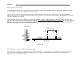
1
ELECRAFT K1 TRANSCEIVER BAND RIT / XIT ELECRAFT ATTN WPM + 1 TX DISPLAY RX MENU XFIL WPM - K 1 TR ANS C EIVER EDIT + 2 ATTN AF GAIN - T RIT MSG XIT [PF1] REC + O W N E R’S M A N U A L ELECRAFT K1 Multiband CW T r a n s c e i v e r Owner’s Manual Revision F, January 24, 2002 Copyright 2002 Elecraft, All Rights Reserved Elecraft • www.elecraft.com P.O. Box 69 • Aptos, CA 95001-0069 LLC (831) 662-8345 • Fax: (831) 662-0830 ELECRAFT 2 Table of Contents 1. INTRODUCTION.................................................................................................................................................................................... 3 2. SPECIFICATIONS ................................................................................................................................................................................ 5 3. PREPARATION FOR ASSEMBLY.................................................................................................................................................... 6 4. FILTER BOARD.................................................................................................................................................................................. 11 5. FRONT PANEL BOARD.................................................................................................................................................................... 17 6. RF BOARD, PART I........................................................................................................................................................................... 25 7. ALIGNMENT AND TEST, PART I ...................................................................................................................................................... 36 8. RF BOARD, PART II.......................................................................................................................................................................... 42 9. ALIGNMENT AND TEST, PART II..................................................................................................................................................... 46 10. FINAL ASSEMBLY............................................................................................................................................................................ 48 11. OPERATION....................................................................................................................................................................................... 50 12. CIRCUIT DETAILS............................................................................................................................................................................. 58 PARTS LIST.............................................................................................................................................................................APPENDIX A SCHEMATIC.............................................................................................................................................................................APPENDIX B BLOCK DIAGRAM..................................................................................................................................................................APPENDIX C PHOTOGRAPHS.....................................................................................................................................................................APPENDIX D TROUBLESHOOTING............................................................................................................................................................APPENDIX E PARTS PLACEMENT DRAWINGS....................................................................................................................................... APPENDIX F QUICK REFERENCE..............................................................................................................................................................APPENDIX G ELECRAFT 3 1. Introduction The K1 is a versatile, low-power CW transceiver that covers two or four builder-selected HF bands. It provides 5 watts or more of power output; excellent receiver sensitivity and selectivity; and many useful operating features, including instant band selection, receive and transmit incremental tuning (RIT/XIT), digital display, configuration menu, and multiple crystal filter bandwidths. Like our all-band K2 transceiver, the K1 uses modular construction, allowing it to adapt to your operating needs. The Filter board covers either two (KFL1-2) or four (KFL1-4) bands, and a different Filter board can be swapped in at any time. There are two plug-in options, including a noise blanker (KNB1) and automatic antenna tuner (KAT1). There's also an internal AA-cell battery option (KBT1). These options can be installed easily at any time. With receive-mode current drain of about 55 mA, built-in keyer, and a stable, low-frequency VFO, the K1 is ideal for portable operation. It's also one of the smallest multi-band HF transceivers available–smaller than many single-band rigs. And, when used with the optional wide-range tilt stand (KTS1), the K1 is truly trailfriendly. The tilt stand comes with long arms for ground-mounting (see below), as well as shorter arms for desk-top use. The K1's modular assembly will also appeal to first-time builders. The kit requires almost no point-to-point wiring, unlike earlier designs that used wiring harnesses. The K1 even provides its own built-in test equipment, including battery voltage monitor, wattmeter, and frequency counter. The manual provides complete troubleshooting and signal tracing procedures, and you’ll find further support on our website, www.elecraft.com. We’d like to thank you for choosing the K1 transceiver, and hope it meets your expectations for operation both at home and in the field. Wayne Burdick, N6KR Eric Swartz, WA6HHQ 4 ELECRAFT Customer Service Information Technical Assistance If you have difficulty with kit construction, operation, or troubleshooting, we’re here to help. You may be able to save time by first consulting our web site, www.elecraft.com, or by posting your question on the Elecraft e-mail forum, [email protected]. Telephone assistance is available from 9 A.M. to 5 P.M. Pacific time (weekdays only) at 831-662-8345. You can also send e-mail to [email protected]. Please use e-mail, rather than call, when possible since this gives us a written record of the details of your problem. Repair Service If necessary, you may return your completed kit to us for repair. Contact Elecraft before mailing your kit to obtain the repair shipping address, as well as information on repair fees. (Kits that have been soldered using acid core solder, watersoluble flux solder, or other corrosive or conductive fluxes or solvents cannot be accepted for repair–see Warranty.) The following information should be provided to expedite repair: your name, address, and phone number; your e-mail address (if applicable); and a complete description of the problem. Shipping: First, seal the unit in a plastic bag to protect the finish from dust and abrasion. Use a sturdy packing carton with 3" or more of foam or shredded paper on all sides. Seal the package with reinforced tape. (Neither Elecraft nor the carrier will accept liability for damage due to improper packaging.) Cover the "to" address label with clear tape. Elecraft’s 1-Year Limited Warranty This warranty is effective as of the date of first consumer purchase. Before requesting warranty service, you should complete the assembly, carefully following all instructions in the manual. What is covered: During the first year after date of purchase, Elecraft will replace defective parts free of charge (post-paid). We will also correct any malfunction caused by defective parts and materials. You must send the unit at your expense to Elecraft, but we will pay return shipping. What is not covered: This warranty does not cover correction of assembly errors or misalignment; repair of damage caused by misuse, negligence, or builder modifications; or any performance malfunctions involving non-Elecraft accessory equipment. The use of acid-core solder, water-soluble flux solder, or any corrosive or conductive flux or solvent will void this warranty in its entirety. Also not covered is reimbursement for loss of use, inconvenience, customer assembly or alignment time, or cost of unauthorized service. Limitation of incidental or consequential damages: This warranty does not extend to non-Elecraft equipment or components used in conjunction with our products. Any such repair or replacement is the responsibility of the customer. Elecraft will not be liable for any special, indirect, incidental or consequential damages, including but not limited to any loss of business or profits. ELECRAFT 5 2. Specifications Measurements were made using a 14-V supply and 50-ohm load. Transmitter General Size (H x W x D) Cabinet Overall 2.2 x 5.2 x 5.6" (5.6 x 13 x 14 cm) 2.4 x 5.2 x 7.1" (6 x 13 x 18 cm) Weight 1.4 lbs. (0.6 kg), excluding options Supply voltage 8.5 to 15 VDC Current drain Receive Transmit 1 55 mA typ. (no signal) 700-900 mA typ. (5 W, 14 VDC) Power output 0-5 watts or higher; spurious and harmonic content -40 dB @ 5 W Load tolerance 2:1 or better SWR recommended; will survive high-SWR operation Sidetone pitch 400-800 Hz in 10 Hz steps Internal keyer 8-50 WPM; Iambic modes A and B; 2 message buffers; auto-repeat Receiver Bands covered (MHz) 3.5, 7.0, 10.1, 14.0, 18.05, 21.0 (2 or 4 selected bands per module) Sensitivity Approx. 0.2 µV for 10 dB (S+N)/N Frequency control I.F. 4.915 MHz, single conversion Selectivity 4-pole variable-bandwidth crystal filter, approx. 200-800 Hz Electronically-tuned 3 MHz VFO; approx. 80 or 150 kHz range, selected during assembly VFO drift < 200 Hz per hour after 5-minute warm-up at 25° C Audio output 1 watt (peak) into 8-ohm load RIT/XIT range Approx. +/- 3 kHz1 Int. speaker 8 ohms, high-efficiency Display 3-digit LCD w/bargraph modes Headphones or ext. speaker 8 ohms or higher; stereo plug (mono optional--see page 31, second assembly step) The RIT/XIT range can be easily modified; see page 55. ELECRAFT 6 3. Preparation for Assembly Overview of the K1 The K1 uses modular design for ease of assembly and troubleshooting. The chassis is made up of five pieces (Figure 3-1), any of which can be removed individually. The RF power amplifier transistor uses the right side panel as a heat sink, so there is no separate heat sink element. Each side panel includes a 10-32 threaded PEM nut as a mounting point for the KTS1 tilt stand. There are three printed circuit boards (PCBs), as shown in Figure 3-2: Front Panel board, Filter board, and RF board. These boards plug in together with no wiring, as explained in the next section. K1 options, such as the KNB1 noise blanker, also plug in directly. Appendix D shows photographs of each completed PC board assembly. Side Panel Filter Top Cover Front Panel Front Panel RF Bottom Cover (Right side panel not shown) Figure 3-2 Figure 3-1 ELECRAFT 7 Board-to-board Connectors The circuit boards in the K1 plug in together using board-to-board connectors, which eliminates nearly all hand wiring. Gold-plated contacts are used on these connectors for reliability and corrosion resistance. Figure 3-3 shows a side view of the PC boards and board-to-board connectors. As can be seen in the drawing, the Front Panel board has a connector J1 which mates with right-angle connector P1 on the RF board. The Filter board has three connectors, P1, P2 and P3, which mate with J6, J7 and J8 on the RF board. These multi-pin connectors are difficult to remove once soldered in place. Refer to Figure 3-3 during assembly to make sure you have each connector placed correctly before soldering. If you install a multi-pin connector incorrectly, clip all of the pins at the body of the device first, remove all of the pins individually, and call us to request a new connector. You may damage pads and traces by trying to remove such components intact. Front Panel Filter Board P1,P2 P3 J6,J7 J1 P1 J8 RF Board Figure 3-3 K1-2 (2-band version) and K1-4 (4-band version) This manual covers all aspects of assembly for the two-band K1 (model K1-2). If you purchased a four-band K1 (model K1-4), you'll use the KFL1-4 assembly manual during assembly and alignment of the Filter board. You'll find instructions specific to the 4-band module at all appropriate places in this Owner's manual. ELECRAFT 8 Unpacking and Inventory Handling Integrated Circuits and Transistors This kit uses integrated circuits (ICs) and transistors that can be damaged by electrostatic discharge (ESD). Problems caused by ESD can often be difficult to troubleshoot. To avoid this: Leave parts in their anti-static packaging until you install them Use an anti-static mat on your work bench Use a soldering iron with a grounded tip Ground yourself using a wrist strap with 1-Mohm series resistor At minimum, touch an unpainted, grounded metal surface before handling ESD-sensitive components Inventory We recommend that you do a complete inventory, using the parts lists in Appendix A. Start with the K1 Packing Box Parts list, which details the items you should find when you first open the box. Additional parts lists are provided for components used in each subassembly. Component photographs are provided in most cases. Identifying Resistors and RF Chokes Resistor and RF choke values and color bands are provided in the text. However, it's helpful to familiarize yourself with the color code. The color-code chart, Figure 3-4, shows how to read the four color bands on 5% resistors. For example, a 1,500 ohm (1.5 k) 5% resistor has color bands BROWN, GREEN, RED and GOLD. 1% resistors are similar, but use five bands: three significant digits, a multiplier, and tolerance. The first four bands on a 1.5 k, 1% resistor are BROWN, GREEN, BLACK, BROWN. The multiplier value is 1 rather than 2 in the this case because of the third significant digit. 1% resistors have color bands that are sometimes hard to distinguish clearly; use an ohmmeter to identify them. The markings on RF chokes reflect their value in microhenries (µH), using two significant digits and a multiplier. Example: a choke with color bands RED, VIOLET, BLACK has value of 27 µH. Color Code Tolerance (gold = 5%, silver = 10%) Multiplier Second Digit First Digit Color Digit Black 0 Brown 1 Red 2 3 Orange Yellow 4 Green 5 Blue 6 Violet 7 Gray 8 White 9 Silver -Gold -- Multiplier x1 x 10 x 100 x 1K x 10K x 100K x 1M Figure 3-4 x .01 x 0.1 ELECRAFT 9 Identifying Capacitors Soldering and Desoldering Small-value fixed capacitors are usually marked with one, two, or three digits and no decimal point. If one or two digits are used, that is the value in picofarads (pF). If there are three digits, the third digit is a multiplier. For example, a capacitor marked "151" would be 150 pF (15 with a multiplier of 101). Similarly, "330" would be 33 pF, and "102" would be 1000 pF (or .001 µF). Exceptions are described specifically in the text and parts list. Use adequate ventilation when soldering, and avoid inhaling smoke or fumes. Always wash your hands after handling solder, as lead residue is highly toxic. Fixed capacitors with values of 1000 pF or higher often use a decimal point in the value, such as .001, .047, or 2.2. This is the value in microfarads (µF). (1 µF is equal to 1,000,000 pF.) Tools The following specialized tools are supplied with the K1: .050" (1.3 mm) and 5/64" (2 mm) Allen wrenches Double-ended plastic alignment tool In addition to the tools supplied, you will need these standard tools: Temperature-controlled soldering iron, 700-800°F (370-430°C) Fine-point soldering iron tip, approx. .05" (spade type) Small-diameter, IC-grade solder (see Solder Recommendations) Desoldering tools (wick, solder-sucker, etc.) Needle-nose pliers Small-point diagonal cutters, preferably flush-cutting Small Phillips and flat-blade screwdrivers DMM (digital multimeter; do not use an analog VOM) Magnifying glass We strongly recommend that you use a conductive wrist strap and anti-static mat during assembly. These items are available at very low cost from Jameco, Mouser, and other electronics suppliers. Solder Recommendations We recommend small-diameter (.02 to .04") rosin-core solder, similar to Kester type 44. Solder with 2% silver is used by some builders and will work equally well. If you use a minimum of solder, there will be no need to clean PC boards. The use of acid-core solder, water-soluble flux solder, or any corrosive or conductive flux or solvent is likely to damage components and/or PC boards. Soldering When applying solder, use the minimum amount required to surround the component lead and make good contact with its printed-circuit pad. You don't need a "fillet" (build-up) of solder. To provide a good connection, the solder must flow onto both the component lead and its PC board pad. To ensure that both will be heated at the same time, the tip of the iron should contact both the component lead and the PC board pad before solder is applied. Solder joints should be clean and shiny. If a joint appears dull or has fine cracks, it is probably cold. Cold solder joints should be cleaned and re-soldered. First, use solder wick (desoldering braid) to remove the old solder. Then apply fresh solder. If you have many cold solder joints, it probably indicates that your soldering iron temperature is too low, or that the tip or solder itself is defective. New soldering iron tips must be tinned before they’re used. Allow the iron to warm up completely, then apply solder and allow it to coat the entire tip. After a few minutes, wipe off the excess solder. Use a sponge for wiping the iron tip, and clean the sponge often. ELECRAFT 10 Desoldering Assembly Notes The printed circuit boards used in the kit are double-sided, meaning that they have circuitry on both sides. The component mounting holes are plated-through to complete electrical connections between the two sides. Each step in the assembly process is accompanied by a check-box: Removing components from double-sided boards can be difficult, since you must get all of the solder back out of the hole before a lead can be removed. To do this, you'll need solder wick (desoldering braid) and/or a vacuum desoldering tool. It also takes some practice. A number of suggestions are provided below. The best strategy for avoiding de-soldering is to place all components properly the first time. Double-check values and orientations, and avoid damaging parts via ESD. When removing components: Don't pull a lead or pin out of a hole unless the solder has been removed, or you are applying heat. Otherwise, you can literally pull out the plating on the plated-through hole. Limit soldering iron contact to a few seconds at a time. Use small-size solder-wick, about 0.1" or 2.5 mm wide. Use the wick on both the top and bottom pads when possible. This helps get all of the solder out of the hole. If you use a vacuum desoldering tool (solder sucker), use a large unit. Small solder suckers are not very effective. The safest way to remove ICs and other components with more than 3 leads is to clip all of the pins at the body of the device first, then remove all of the pins individually. You may damage pads and traces by trying to remove such components intact. Invest in a PC board vice with a heavy base if possible. This makes parts removal easier because it frees up both hands. If in doubt about a particular repair, ask for advice from Elecraft or from someone else with PCB repair experience. This symbol is used to alert you to important information: i Do not skip any steps. You may adversely affect both the performance and appearance of the kit by using the wrong assembly order. Components Sometimes we refer to components by their PC board and reference designator. For example, "FP-Q1" refers to transistor Q1 on the Front Panel board. A few components in the kit are mounted on the bottom of PC boards. Component outline symbols are provided on the appropriate side of the board, so it will always be clear which side a particular component goes on. Bottom-mounted parts are also identified on the schematics by this symbol: Photographs Before beginning assembly, you should review the photographs in Appendix D to get an idea of what the completed PC boards look like. You'll also find front and back views of each PC board in the Parts Placement Drawings, Appendix F. ELECRAFT 11 4. Filter Board This section applies only to the two-band K1 Filter board. If you have a four-band K1, refer to the assembly instructions in the KFL1-4 manual. The Filter board determines the K1's bands of operation. A photograph of the completed board appears in Appendix D. Open the bag of components labeled FILTER BOARD and sort the parts into groups. Identify components using the photographs in the Filter board parts list in Appendix A. Locate the Filter printed circuit board (PCB), labeled "K1 FIL2" on one side. With the top side of the PC board facing you (notch at the lower right), locate the position of resistor R1, along the front edge. The label "R1" appears just left of the resistor’s outline. Install a 100-ohm, 5% resistor (brown-black-brown) at R1, with its first color band (brown) toward the left. Make sure it is seated flat on the board, then bend the leads outward at about a 45degree angle to hold it in place. Solder R1 on the bottom of the board. Trim the leads as close as possible to the solder joints. i Components may be soldered one at a time or in groups. Leads can be trimmed either before or after soldering. Install an 18-pin IC socket at U1, with the notched end of the socket oriented towards the "K1 FIL2" label. Bend two leads of the socket outward slightly to hold it in place while soldering. (U1 itself will be installed in a later step.) i In the following steps you'll install three relays (K1-K3). Relay pins must not be bent, even after placement on the PC board, as this may cause unreliable mechanical operation. Place relays K1-K3 on the top side of the board. One end of each relay has a heavy line printed across the top to indicate the pin 1 end. This end must be matched with the same end of the relay’s PC board outline. Do not solder the relays yet. When all three relays have been placed on the board, lay a flat object such as a book or piece of cardboard on top of the relays to keep them in place, then flip the board over. Solder only two pins (at opposite corners) on each relay, using a minimum amount of solder. Limit soldering time to 2 or 3 seconds per pin. Do not bend or trim the leads. Turn the board back over and verify that all of the relays are in the correct orientation and are seated flat on the board. To check the orientation, refer to the Filter board drawing in Appendix F, at the bottom of the page. Solder all of the remaining relay pins. Do not bend or trim the leads. ELECRAFT 12 Install the capacitors listed below. The list shows the capacitance value, followed by the labeling (in parentheses). After installing each capacitor, bend the leads outward at about a 45degree angle to hold it in place until it is soldered and trimmed. __ C29, .001 (102) __ C30, .001 (102) At this point you’ll need to choose whether to set up the VFO for 80-kHz or 150-kHz coverage (approx.). The smaller range covers the most-used portion of every band, provides smoother tuning, and is strongly recommended if you plan to upgrade to the four-band module (KFL1-4), which has narrower band-pass filters. __ C27, .047 (473) Record your VFO range selection here for reference: Place a bookmark at this page, and another at the Per-Band Components table in Appendix A. Locate the two bags of per-band components, which are labeled by band, e.g. "40m" or "K1B40" (40 meters). Under Reference Designators in the Per-Band Components table, there are Band 1 and Band 2 columns. Fill in the blanks at the top with your two bands (e.g., "40" and "20"). The lowerfrequency band should be designated as Band 1. Using strips of paper, or labels with a light adhesive such as “post-its,” temporarily cover the band 2 reference designators column. Similarly, cover all of the components columns except the column associated with band 1. This is a very important step that will eliminate possible confusion during assembly. Open the bag of components for band 1 only, setting the band 2 components aside for now. i The leads on small capacitors may be pre-formed so that the capacitor sits slightly above the board when inserted; this will not affect performance. The leads are also somewhat fragile. Install the capacitors for band 1, using the reference designators and values from the appropriate columns in the parts list. For example, if band 1 is 40 meters, install 390-pF capacitors at C1 and C5, then 330 pF capacitors at C2 and C4, etc. Doublecheck each capacitor value as it is installed. Do not solder yet. Solder all of the band 1 capacitors. ___ 80 kHz ___ 150 kHz Note: Two different crystals are supplied for 30 meters, corresponding to two different lower band edges. Which one to use depends on your selected VFO range (see below). In the following steps you’ll select one of the two crystals when applicable. Band 30 Meters VFO Range 80 kHz 150 kHz Crystal 18.100 18.000 Band Edge 10.100 10.000 If band 1 is 30 meters, select the appropriate crystal using the table above. Save the other crystal for possible future use. Install the band 1 crystal at X1 on the filter board (to the right of X2), bending the leads to hold it in place. Make sure the crystal is seated correctly, then solder. Use a minimum amount of solder to avoid a short under the can. Move the strips of paper or labels that you used earlier so that they cover the band 1 reference designators column, and all of the components columns except the column associated with band 2. Open the components bag for band 2. Install the band 2 capacitors, using the reference designators and values from the appropriate columns as before. (Example: if band 2 is 20 meters, you'll install 180-pF capacitors at C6 and C10, etc.) Locate the band 2 crystal and verify that it is the correct frequency. If band 2 is 30 meters, select one of the two crystals supplied (see table above). Install it at X2 and solder. ELECRAFT 13 Cut two 3/4" (19 mm) bare wires (use component leads). Referring to Figure 4-1, insert bare wires into the grounding holes provided near X1 and X2. Fold each wire over the top of the crystal and solder it on top. Keep soldering time below 5 seconds at a time; if it takes longer, your iron may not be hot enough, or your iron tip may not be making good contact with the crystal can. Solder and trim the wires on the bottom of the board. At the left and right ends of the board you’ll find two short jumper locations, each labeled with a ground symbol ( ). Use component leads to make 3/4" (19 mm) U-shaped wires for each jumper (Figure 4-2). Solder the jumpers on the bottom of the board, with the top of the U-shape approx. 1/4" (6 mm) above the board. Top side X1 X2 Figure 4-2 Figure 4-1 Install the ceramic resonator, Z1, to the right of U1. (The ceramic resonator looks like a capacitor with three pins, and can be oriented in either direction.) Limit soldering time to 2 or 3 seconds on each pin to avoid altering the oscillation frequency. Locate the eight 1-µH slug-tuned inductors, and make sure they are all be labeled "T1050". Install the inductors at L1 through L8, pressing each one down as far as it will go. They have five pins, plus ground tabs, and can only be installed on the board one way. Solder the inductors. Identifying Toroid Cores Several toroidal inductors are used in the K1, including four on the Filter board. It is important to use the correct type of core. This can be determined from the color and size. The cores used on the Filter board are type T37-6. The T identifies an iron-powder core. The number following the T specifies the outside diameter in hundredths of an inch, in this case 0.37 inches (9.4 mm). The suffix (-6) refers to a specific mix of iron powder, which uses a particular color, in this case yellow. Later in assembly you'll encounter ferrite cores, for example type FT50-43. In this part number, FT identifies the core as ferrite, and 50 is the size (0.50", 12.5 mm). The suffix (-43) identifies the type of ferrite used, although all ferrite cores are dark gray in color. All ferrite cores used in the K1 are of the -43 type. ELECRAFT 14 i In the following steps you’ll install toroidal inductors L9L12 (type T37-6 cores). They must be wound as indicated in the instructions, or the transceiver will not operate correctly. Use only the number of turns specified. It is not necessary to attempt to precisely match the inductances specified in the parts list. Verify that the turns of L9 are not bunched together. They should be evenly spaced, and should occupy about 80-90% of the core. Find the component outline for L9 on the Filter board. Compare this component outline to Figure 4-3, which shows two views of a typical toroidal inductor. L9 will be mounted vertically as shown at the right side of the drawing, with one wire exiting at the core’s upper left, and the other at the lower right. There are pads on the PC board in these two locations. The enamel wire supplied with the kit can be heat-stripped. One way to do this is to place a small amount of solder (a "blob") on the end of your soldering iron, then insert the wire into the hot solder. If the iron is hot enough, you should see the insulation vaporize after 3 to 6 seconds. Another possibility is to burn the insulation off by heating it with a small butane lighter for a few seconds, then use fine-grain sandpaper to remove the enamel residue. Avoid scraping insulation off with a razor blade, as this may nick the wire. Using the Per-Band Components parts table (Band 1), determine the number of turns and wire length for L9 and L10. To wind L9, cut the specified length of #26 red enamel-coated wire, then "sew" the long end of the wire through the core. Each pass through the core counts as one turn. The finished winding should look similar to Figure 4-3, but with the number of turns indicated in the parts list. Figure 4-3 shows 14 turns. Stripping Toroid Leads Strip the leads of L9, as explained above. You should remove the enamel from the leads up to about 1/8" (3 mm) from the core (Figure 4-3). Tin L9's leads. The solder should appear clean and shiny. If it looks dull or is not adhering very well to the bare lead, there is probably some insulation remaining. Remove it as described above. Install L9 vertically as shown by its component outline. Pull the leads taut on the bottom of the board. Solder the leads of L9. When soldering, make sure that the solder binds well to the leads. If the lead appears to be an "island" in a small pool of solder, chances are it is not making good contact. Wind and install L10 in the same manner as L9, using the same number of turns. Install L10 vertically, to the right of L9. Wind and install L11 and L12. Use the Per-Band Components table (Band 2) to look up the wire length and number of turns. Remove insulation Figure 4-3 i Do not use adhesives or fixatives of any kind to secure L9L12 to the PC board. They will be adequately held to the board by their leads alone. ELECRAFT 15 i The connectors to be installed in the following steps must be positioned correctly to avoid intermittent or unreliable operation. Before attempting to install multi-pin connectors, review the information on page 7. Cut a 1" (25 mm) length of insulated hookup wire. Strip about 1/8" (3 mm) of insulation off of each end. Install this wire between pins 2 and 10 of J2, in the upper righthand corner of the board (Figure 4-5). The pins on J2 are counted from left to right and top to bottom as shown. Install an 8-pin male connector (plug) at P1, but do not solder yet. Figure 4-4 shows P1 as viewed from the left end of the Filter board. The plastic part of the connector must be on the bottom side of the board, with the long end of the pins pointed down. The short pins are inserted into the board. 1 2 9 10 J2 Figure 4-5 i Before handling U1 in the next step, touch an unpainted, grounded metal surface. P1 Figure 4-4 Solder just one of the middle pins of P1, on the top side. Note: multi-pin connectors have plastic bodies that can melt if too much heat is applied, causing the pins to be mis-positioned. Limit soldering time for each pin to 2 to 3 seconds. Straighten the leads of U1 (PIC16C620) as shown in Figure 4-6. The two rows of pins must be straight and parallel to each other to establish the proper pin spacing. To straighten the pins, rest one entire row of pins against a hard, flat surface. Press down gently on the other row of pins and rock the IC forward to bend the pins into position as shown below. Flared Examine the placement of P1 closely. If it is tilted or is not flat against the board, re-heat the solder while pressing down on the connector. Straight Once P1 is in the right position, solder the remaining pins. Do not trim the leads. Figure 4-6 Install P2 and P3 in the same manner as P1. Before soldering, verify that each connector is flat against the board and not tilted. ELECRAFT 16 Insert U1 into its socket, with the notched or dimpled end of the IC aligned with the notched end of the PC board outline. (Figure 4-7 shows an 8-pin IC; U1 is similar but has 18 pins.) Press U1 down into the socket as far as it will go. Visual Inspection Using the parts placement drawings in Appendix F, re-check the orientation of the relays (K1, K2, K3) and U1. i Notch Pin 1 Dimple Pin 1 Figure 4-7 Note: IC pins are counted by going around the IC counterclockwise from pin 1. Examine U1 closely. If any pins are bent, remove the IC and straighten them. (To remove U1 from its socket, pry it up gently on each end using a small flat-blade screwdriver.) Locate the blank white area near U1. This area is provided for labeling the Filter board with the two bands covered (e.g. "40, 20"). Use an indelible marker, dry transfers, or an adhesive label. Uninstalled Components All component locations on the Filter board should now be filled except J1 and J2, which are provided for the automatic antenna tuner (KAT1). The KAT1 option should be installed only after the basic K1 kit has been completed and tested. At that time, the jumper you installed between pins 2 and 10 of J2 will be removed. About 90% of all problems with kits are caused by poorlysoldered component leads. Such problems can be avoided by doing a careful inspection of the board, preferably with a magnifying glass. Examine the bottom of the PC board closely for cold solder joints, solder bridges, and unsoldered components. Resistance Checks Make the measurements listed below, touching the meter's (+) and (-) leads to the indicated points. Measurements at relay K3 must be made on the bottom side. Relay pins are numbered like ICs, with pin 1 identified by its round pad. The Filter board schematic (in Appendix B) may help you troubleshoot any incorrect readings. i The symbol > means greater than, and < means less than. Your DMM may indicate infinite resistance (all digits flashing) for readings that are listed as "> 100 k." (Do not use an analog VOM.) Test Points (+, -) U1 pin 6, U1 pin 7 U1 pin 6, U1 pin 8 U1 pin 6, U1 pin 12 U1 pin 13, P2 pin 6 P1 pin 1, P1 pin 3 P1 pin 2, P1 pin 3 P1 pin 3, P1 pin 4 P1 pin 3, P1 pin 6 P2 pin 1, P2 pin 2 P2 pin 7, P2 pin 8 K3 pin 2, K3 pin 9 K3 pin 4, K3 pin 7 Resistance 230-270 ohms 230-270 ohms 230-270 ohms 90-110 ohms > 100 k > 100 k > 100 k > 100 k > 100 k > 100 k < 5 ohms < 5 ohms ELECRAFT 17 5. Front Panel Board The liquid-crystal display (LCD), switches, and other controls are located on the Front Panel board, as well as the microcontroller. See Appendix D for photos of the completed assembly. Open the bag labeled FRONT PANEL and sort the parts into groups. Observe anti-static precautions with ICs and transistors. Locate the front panel PC board, which is labeled "K1 FP" along one edge. In the steps that follow, we will refer to the side with the switches and LCD (S1-S6 and DS1) as the top side. Place the board in front of you with the bottom side up. Locate the component outline for J1, below the large hole. Install a 20-pin female connector (receptacle) at J1 as shown in Figure 5-1. Do not solder yet. Solder one pin of J1 on the top side, near the middle of the connector. If J1 is not seated flat against the PC board or is tilted, re-heat the solder and press down on the connector. Once you're sure that J1 is correctly installed, solder the remaining pins. Do not use an excessive amount of solder. Locate the Switch Spacing Tool (made of PC board material). Position push-button switch S1 on the top side of the board as shown in Figure 5-2, using the switch spacing tool to set the switch height. Make sure all four legs of the switch are centered in their holes, then gently push the switch until it is resting flush against the switch-spacing tool. (Caution: switch pins are fragile.) Do not solder yet. S1 Bottom side Top side (with LCD) J1 Figure 5-2 Figure 5-1 ELECRAFT 18 Top of board 1/16” Figure 5-3 Figure 5-3 shows a side view of a switch that is properly mounted (spacing tool not shown). The leads of the switches will just be visible on the bottom of the board. Proper switch height is important for maintaining an even appearance. Once S1 is seated correctly, solder the leads on the bottom side of the board. Leave the spacing tool in place while soldering. Install S3, once again using the switch spacing tool to adjust the switch height. When soldering S3, be careful not to contact the plastic body of J1 with the soldering iron. Install switches S2, S4, S5, and S6 using the same technique. Note: Switch caps will be installed later. Install these parts on the top side of the board. Solder them on the bottom side, using a minimum of solder. __ R8, 22 (RED-RED-BLK) __ C4, .047 µF (473) Trim the leads of R8 and C4 as close to the board as possible so that they won't interfere with the 40-pin IC socket (next step). Install the 40-pin IC socket at U1, on the bottom side of the board. The board is labeled "SOCKET" at this location. Orient the socket's notched end to the left (the pin 1 end). To hold the socket in place, bend pins 1 and 21 outward slightly; these two pins are diagonally opposite. Solder only these two pins. If the socket does not appear to be seated flat on the PC board, reheat these two pins while pressing on the socket. If the leads of C4 hit the socket, trim them closer to the board. Solder the remaining pins of U1. (U1 itself will be installed in the socket in a later step.) Install and solder the following components. When soldering components near the push-button switches, be careful not to touch the switches with the soldering iron. Top side: __ R4 and __ R5, 10 k (BRN-BLK-ORG) __ R11, 100 k (BRN-BLK-YEL) Bottom side: __ R6, 12.7 k, 1% (BRN-RED-VIO-RED) __ R7, 3.92 k, 1% (ORG-WHT-RED-BRN) __ R9, __ R10, and __ R19, 100 k (BRN-BLK-YEL) __ R13, 470 (YEL-VIO-BRN) __ R12, 2.7 k (RED-VIO-RED) __ R14 and __ R15, 1 k (BRN-BLK-RED) __ R16, 2.7 k (RED-VIO-RED) __ C5 and __ C6, .01 µF (103) Install capacitors C1 and C2 (82 pF), near U1. Locate resistor network RP1. ("RP" means "resistor pack," another name for resistor networks.) One end of RP1 has a dot, indicating pin 1. RP1 should be labeled 77083102, 83C102, or 8A3102G. If the labeling differs, verify the resistance. You should measure about 1.0 k between each pair of adjacent pins. Install RP1 on the bottom side of the board. The end with a dot or bar should be oriented towards pin 1 of the PCB outline. When soldering RP1, keep the iron tip away from S4 and S5. Install and solder the two 82-µH RF chokes, RFC1 and RFC2 (GRAY-RED-BLK). ELECRAFT 19 i Before handling ICs and transistors in the following steps, touch an unpainted, grounded metal surface. Locate transistor Q1 (type 2N4124), which has a small, 3-lead TO-92 package. Q1 and other TO-92 devices may have either of the two shapes shown in Figure 5-4. The right-hand illustration shows a "modified TO-92" package, which may be labeled on either the front or back side. The large flat side of each device will be aligned with the flat side of its component outline. Locate U4, a 78L06 voltage regulator, which has a TO-92 package similar to Q1. Install U4 below the large hole. i Touch an unpainted, grounded metal surface before handling the 2N7000 transistor in the next two steps. Locate the component outline for Q2 (2N7000) on the top side of the board near the rectangular hole. Q2's outline has the three pins side-by-side, not in a triangular pattern. Pre-form the leads of Q2 to match this hole pattern, so that it can be mounted very close to the PC board with little excess lead length. Install Q2. Make sure the top of Q2's body is no more than 0.25" (6 mm) above the board when seated. Solder Q2. Install the 8-pin ICs, U2 (MAX518), U3 (24LC04), and U5 (LM358) on the bottom side. Orient the notched or dimpled end of each IC with the notched end of its component outline (see Figure 4-7). Bend two leads outward slightly on the opposite side of the board to hold the devices in place, but do not solder yet. Figure 5-4 Turn to Appendix F (parts placement drawings) to verify that you have the ICs installed in the proper locations, then solder. Limit soldering time to 2 to 3 seconds on each lead. Install Q1 on the bottom side of the board, to the right of the large hole. Align Q1 as shown above. The transistor should be mounted about 1/8" (3 mm) above the board; don’t force it down too far or you may break the leads. Bend the leads outward slightly to hold Q1 in place, then solder and trim the leads. On the top side of the board at the left end you’ll find a short jumper location, labeled with a ground symbol ( ). Install a 3/4" (19 mm) U-shaped wire here, as you did earlier on the Filter board. i The potentiometers to be installed in the next step can be damaged if you push on their plastic shafts. When seating a potentiometer, press down only on the metal frame. Install the two 10-k potentiometers at R2 and R3 (on the top side of the board). They must be pressed downward until the metal frame is fully contacting the PC board on both sides. Do not use excessive heat when soldering. ELECRAFT 20 Open the bag labeled MISCELLANEOUS and empty the contents into a shallow box or pan. This will prevent loss of any of the small hardware while allowing you to locate items as needed. Top Side i Five sizes of 4-40 screws are used. All are black anodized except the 1/4" and 3/8" pan heads (see Figure 5-5). The length of flat-head screw is measured from the top of the head. Pan-head, 1/4” (6 mm) Figure 5-6 Pan-head, 3/8” (9.5 mm) Install crystal X1, near C1 and C2 on the bottom of the board. Pan-head, 3/16” (4.8 mm) To the right of X1 you'll find a ground pad for the crystal can. Use a discarded component lead to make the grounding wire, as shown in Figure 4-1 (page 13). Flat-head, 3/16” (4.8 mm) Locate LEDs D1 and D2, which are identical in size but have different-colored bodies. D1 has a clear diffuse body, while D2 has a yellow tint. Near the point where the leads exit the body, you'll find a flat side in the plastic, which identifies the cathode lead. Flat-head, 5/16” (8 mm) Figure 5-5 Identify all of the 4-40 screws and sort them into groups. Install a 3/16" (4.8 mm) diameter x 1/4" (6.4 mm) long round standoff on the top of the board (Figure 5-6). The hole for this standoff is just below the large hole. Use two #4 split lock washers and a 1/4" (6 mm) pan-head screw (not black anodized) as shown. Insert the lock washers between the standoff and PC board. Install D1 (clear diffuse body) on the top side of the board, with its flat side aligned with the flat side of the component outline. (This is the side nearest the square pad.) Position D1 about 1/16" (1.5 mm) above the board. You can use the switch-spacing tool, a toothpick, or short length of insulated hookup wire to maintain the proper spacing while soldering. Verify the orientation of D1's flat side, then solder. Install and solder D2 using the same method. ELECRAFT 21 Inspect the solder side of U1's socket on the top side of the board. Make sure all pins are soldered, with no cold solder joints. Using a DMM, check every pair of adjacent pads on U1 on the top side of the board (pins 1-20 and 21-40). The resistance between pads should be over 1000 ohms (1 k) in all cases, and may read infinite on your DMM (often indicated by a flashing display). i Caution: the LCD (DS1) and its pins are fragile. Remove the LCD from its packing materials, being careful not to bend the pins. As shown in Figure 5-8, the pin 1 end of the LCD glass has a very slight bump, along with a break in the black border. This end will be oriented towards the pin 1 end of DS1's component outline. i 24 Before handling U1 in the next step, touch an unpainted, grounded metal surface. Straighten the pins of the microcontroller, U1. You can hold the IC body at the ends as you re-form each row of pins. 13 Bump Insert U1 into its socket, with the notched end oriented towards the pin 1 end of the component outline. Look at both rows of pins on U1 closely. If any pins are bent, carefully remove the IC by prying at both ends using a small flatblade screwdriver. Straighten the pins using long-nose pliers. Locate the black neoprene LCD spacer (MISC. bag), which is 1/2 x 1/2 square and 3/16" thick (12 x 12 x 5 mm). Remove the adhesive backing from one side and position the spacer as shown in Figure 5-7. It must be mounted flat against the PC board, centered between the two rows of pins on U1's socket. DS1 1 12 Figure 5-8 Remove the adhesive backing from top side of the LCD spacer. Install the LCD at DS1, oriented as shown above. Make sure that all 24 pins are inserted into their holes, then press down gently on the LCD to secure it to the LCD spacer's adhesive surface. The LCD pins may not extend all the way through the holes. The surface of the LCD must be parallel to the PC board. Once the LCD is positioned correctly, solder all pins. Spacer Figure 5-7 ELECRAFT 22 Visual Inspection Type 1 Using the parts placement drawings in Appendix F, re-check the orientation of the LEDs (D1 and D2), LCD (DS1), and all ICs. Type 2 Examine both sides of the PC board closely for solder bridges, cold solder joints, or unsoldered components. CCW Resistance Checks CW Set both potentiometers to their mid-points. Resistance > 100 k > 100 k > 100 k > 100 k 90-200 k > 100 k < 50 k 15-18 k > 100 k Front Panel Final Assembly Cut three 1.25" (32 mm) lengths of hookup wire. Remove 1/4" (6 mm) of insulation from both ends of each wire. Locate the 10-turn potentiometer, R1. Look closely at Figure 5-9, which shows the positions of the three lugs. The lugs may be labeled 1, 2, and 3, or S, CW, and CCW. 10-turn potentiometer labeling can be confusing, so use the drawing to identify the lugs. Your potentiometer may be either of the two types shown. 2 3 1 2 3 R1 The resistance measurements shown below can all be made from the top side of the board. The (-) lead of your DMM should be connected to the ground jumper ( ) at the left side of the board. Test Points (+) DS1 (LCD) pins 1-24 J1 pin 6 J1 pin 7 J1 pin 8 J1 pin 10 J1 pin 12 J1 pin 15 J1 pin 16 J1 pin 19 1 S 1 2 3 R1 Figure 5-9 Attach the prepared wires to the three lugs Each wire should be wrapped around its lug, leaving the other end free. (Do not solder yet.) R1’s plastic body can be damaged if you apply too much heat to the lugs. Solder the three lugs, limiting soldering time to about two seconds each. Insert R1 through the large round hole in the Front Panel board, rotating it into approximately the position indicated above. Make sure that none of the lugs are touching the PC board. Near the large hole in the board, you'll find three pads for R1's leads (labeled 1, 2, and 3). Referring to Figure 5-9, insert the potentiometer's wires into their corresponding holes. Do not solder yet. i Caution: If the leads of R1 are not connected to the correct pads, the potentiometer is very likely to be damaged. Re-check the connections, then solder R1's leads on the top side of the board. Avoid touching nearby parts with the iron. ELECRAFT 23 Install caps on switches S1 through S6. S3's cap is square, while the others are rectangular, as shown in Figure 5-10. The caps are installed by pressing them onto the switch plungers. After removing any masking tape, turn the front panel face up, with the Elecraft logo at the top. Position the clear plastic LCD bezel over the large LCD opening, then secure it with four 2-56 screws (stainless steel) as shown in Figure 5-11. Tighten the 2-56 screws only the amount needed to hold the bezel to the front panel. Over-tightening may crack the bezel or strip the threaded holes in the panel. Figure 5-10 2-56 Screw (4) i The LCD's glass surface is protected by a very thin, nearly invisible piece of protective film. In the following step, be very careful to remove only the thin film, not the LCD's glass top. Do not use any type of metallic tool. Hold the Front Panel PC board assembly under a strong light so that you can see the surface of the LCD glass clearly. Using a fingernail, rub one corner of the LCD's glass top to loosen the protective film, then peel it off. Locate the front panel chassis piece. Place it on a soft cloth to protect the finish and labeling. Some holes in the front panel are masked on the inside surface during painting. If masking tape (usually green in color) is still present, you'll need to remove it. To remove masking tape: Use a blunt instrument such as a ball-point pen to push on the tape through a hole until the tape begins to lift away. Peel the tape off, using a sharp tool if necessary. Be careful not to scratch the outer surface of the panel. LCD Bezel Figure 5-11 Remove all hardware from the shaft of the 10-turn potentiometer (R1). It will be re-attached in a later step. Locate the 0.75" (19 mm) diameter nylon washer. Place this washer over R1's threaded bushing. ELECRAFT 24 Insert the Front Panel PC board assembly into the front panel (Figure 5-12). The push-button switch caps should protrude slightly. i The Allen wrenches are located in a small bag with the MISCELLANEOUS items. These wrenches may have been oiled during manufacturing. Remove the wrenches and wipe off the oil, if any, then discard the bag. Use the larger Allen wrench (5/64" [2 mm]) to tighten the two set screws on the large knob. Set the AF GAIN and RIT/XIT potentiometers to midway in their rotation, and place a small knob on each. Do not push down hard on the knobs, as this may damage the potentiometers. Tighten each knob's two set screws using the smaller Allen wrench (.050" [1.3 mm]). Align the pointers per panel labeling. Figure 5-12 The 1/4" (6.4 mm) standoff on the PC board should now be visible through the countersunk panel hole just below R1. Secure the panel to the standoff with a 3/16" (4.8 mm) flat-head screw. i Caution: The 10-turn potentiometer may have a plastic bushing. In the following step, do not over-tighten the nut or you may strip the threads. Use the nut and lock washer supplied with R1 to secure it to the front panel. It should be just tight enough to keep R1 from rotating. Place the large knob on R1's shaft. Push the knob on until it just touches the bushing. If the knob does not spin freely, move it out slightly. If the shaft or knob appears to be tilted, the large nylon washer may not be positioned correctly (behind the panel). i At this point in the assembly, the push-button switches may not all protrude an equal distance. The switch height will become equalized once the front panel assembly is mated to the RF board in a later step. i When you rotate the VFO knob, you may hear a faint sound produced by the wiper of the 10-turn potentiometer as it moves across its resistance element. This is normal. Uninstalled Components All component locations should now be filled. ELECRAFT 25 6. RF Board, Part I In Part I, the VFO (variable-frequency oscillator) and receiver sections will be assembled. Open the bag labeled RF and sort the components into groups. Observe anti-static precautions when handling transistors and ICs. Locate the RF board and orient it as shown in Figure 6-1. This illustration shows the major areas of the board. Receiver and VFO circuits occupy the front half; transmitter and T-R switch stages use the rear half. The Filter board plugs into J6, J7, and J8. Turn the board over. (Figure 6-2 shows the bottom side.) Four 2-D fasteners will be attached to the RF board at the indicated locations to secure it to the chassis panels. J8 T-R Switch and Transmitter J6 J7 2-D Fastener VFO Receiver AF Amp Figure 6-1 Figure 6-2 ELECRAFT 26 Locate a 2-D fastener and hold it vertically (Figure 6-3a). Looking at a side with two holes, note that the holes are offset from the center. The PC board outlines for the 2-D fasteners have a matching offset, which will aid in installing them in the next step. i In the steps that follow you’ll install the connectors that mate with the Filter and Front Panel boards. These connectors must be installed properly to ensure reliable mechanical connection. They are difficult to remove once installed, so follow all instructions carefully. Review Figure 3-3 before proceeding. Install an 8-pin female connector at J6, on the top side of the RF board. It must be flush with the board and not tilted (Figure 6-4). Solder just one pin near the center of J6. Holes offset from center J6 (a) (b) Figure 6-3 Install 2-D fasteners at the four locations indicated in Figure 6-2, on the bottom of the RF board. Secure each fastener from the top side of the board with 3/16" (4.8 mm) pan-head screws and #4 split lock washers (Figure 6-3b). Make sure that the 2-D fasteners line up with the edges of the PC board and do not hang over. If they hang over or do not match their component outlines, they are installed backwards. Install relay K1, near the center of the board. Make sure the pin 1 end (with the heavy line) is oriented as indicated by K1’s component outline. Do not bend or trim the relay leads. Figure 6-4 If J6 does not appear to be completely flush with the board, or it is tilted, re-heat the soldered pin and press down. Do not solder the remaining pins yet. Install J7 and J8 in the same manner as J6, soldering just one pin in each case. The Filter board can now be used to check for proper installation of the three 8-pin connectors. Place the Filter board above the connectors (do not plug it in). Verify that all pins of P1, 2, and 3 on the Filter board align with the corresponding holes of J6, 7 and 8 on the RF board. Remove the Filter board. Solder all remaining pins of J6, 7, and 8 on the bottom of the RF board. ELECRAFT 27 Position 20-pin male right-angle connector P1 on the bottom of the RF board (Figure 6-5), but do not solder yet. Review Figure 3-3 for correct placement. The short ends of the bent pins are inserted into the holes, and the long ends are parallel to the board. Top of board Front edge Install the resistors listed below. R23 is at the left-front edge. __ R23, 1.5 Ω (BRN-GRN-GOLD) ⇒ __ R21, 2.7 k (RED-VIO-RED) __ R2, 100 k (BRN-BLK-YEL) __ R17, 120 (BRN-RED-BRN) __ R14, 2.7 k (RED-VIO-RED) __ R7, 680 (BLUE_GRAY-BRN) __ R13, 2.2 M (RED-RED-GRN) __ R16, 75 (VIO-GRN-BLK) __ R18, 75 (VIO-GRN-BLK) __ R1, 1.8 k (BRN-GRAY-RED) These resistors start on the left edge of the board near J6: P1 Figure 6-5 Solder just the two end pins of P1. Make sure that the front-panel assembly can be plugged into P1 as shown in Figure 3-3. Then unplug the front panel assembly. Look closely at P1 to make sure that its plastic support is pressed down as far as it will go, and that the pins are parallel to the board. If not, re-heat the soldered ends while pressing it into place. Once it is seated properly, solder the remaining pins. i In the steps that follow, you'll be installing larger groups of components. When working from a long list, install all of the items on one line before moving on to the next. Arrows (⇒) appear in the list to remind you of this order. In general, assembly proceeds from left to right across the board. Note: All components mounted in the T-R switch and transmitter areas must be kept as low-profile as possible since the Filter board will be plugged in directly above. __ R19, 39 k (ORG-WHT-ORG) __ R9, 2.7 k (RED-VIO-RED) ⇒ __ R20, 20 k (RED-BLK-ORG) __ R26, 1.8 k (BRN-GRAY-RED) __ R34, 100 k (BRN-BLK_YEL) (at the back-right edge near J8) The following capacitors are all of the disc or monolithic type. Start with C26, which is on the left edge close to J6. Note: C65 (22 pF) may be labeled "220J" (see top of page 9). __ C26, 39 (39) ⇒ __ C41, .047 (473) __ C25, .01 (103) __ C6, .01 (103) __ C18, .01 (103) __ C64, .01 (103) __ C32, .047 (473) __ C27, 39 (39) ⇒ __ C30, .047 (473) __ C7, 39 (39) __ C69, 220 (221) __ C74, .01 (103) __ C68, 0.1 (104) __ C42, 220 (221) __ C40, .01 (103) __ C4, .01 (103) __ C72, .01 (103) __ C73, 0.1 (104) __ C17, .01 (103) __ C70, 0.1 (104) __ C75, .01 (103) __ C61, .047 (473) __ C66, .01 (103) __ C39, 220 (221) __ C36, .01 (103) __ C71, 0.1 (104) __ C63, 330 (331) __ C24, .047 (473) __ C21, .01 (103) __ C37, .01 (103) __ C34, 0.1 (104) __ C23, .01 (103) __ C65, 22 (22, 220J) __ C19, .001 (102) __ C22, .001 (102) __ C38, 220 (221) __ C28 and __ C29, .001 (102) __ C49 and __ C48, .01 (103) __ C45, .01 (103) (back-left corner of the board) (back-right corner) (near J4, which is on the back edge) 1200-pF polystyrene capacitor C11 (labeled “1200J”) has axial leads, like a resistor. Note: the kit also includes a 120 pF polystyrene ("120J"). Install C11 in the VFO area of the board, near J6. Limit soldering time to 2-3 seconds. ELECRAFT 28 Install the resistor networks listed below, checking the part numbers carefully before installation. Orient the black dot or bar on each network towards pin 1 of its component outline. __ __ __ __ __ __ RP3, 47 k, 10 pins (10A3473G, 103C104, or 770103473) RP1, 100 k, 8 pins (8A3104G, 83C104, or 77083104) RP2, 100 k, 8 pins (8A3104G, 83C104, or 77083104) RP6, 27 k, 6 pins (6A3273G, 63C273, or 77063273) RP4, 3.9 k, 6 pins (6A3392G, 63C392, or 77063392) RP5, 3.9 k, 6 pins (6A3392G, 63C392, or 77063392) Install a 33-µH RF choke (ORG-ORG-BLK) at RFC1, near the front edge of the board. (Orange bands may appear to be brown.) Install a 100-µH RF choke (BRN-BLK-BRN) at RFC4, in the transmit area of the board. The ceramic trimmer capacitors (C13 and C20) have one side that is flattened. This side must be oriented towards the flattened side of the component outline. Install C20 near the front edge of the board, and C13 in the back-left corner. Sort the diodes into groups for identification purposes. You should have two types of small glass-bodied diodes: 1N5711, and 1N4148. The 1N4753 zener diode may also be glass, and is larger. If necessary, use a magnifying glass to read the labels. i Diodes with long axial leads (such as the types mentioned above) must be installed with the banded end (cathode) oriented towards the banded end of their component outlines. If a diode has more than one band, the widest band indicates the cathode end. Install 1N4148 diodes at D17 and D1, observing the proper orientation as explained above. Do not solder yet. D17 and D1 are both near RP2, in the VFO area. Install 1N5711 diodes at D2 and D15, but do not solder yet. D2 is in the VFO area. D15 is in the back-right corner near J8. Re-check the orientation of the diodes, then solder. Identify the two types of black, axial-lead diodes: 1N4007 and SB530. The 1N4007 is the smaller of the two. Install the SB530 diode at D16, near the back edge of the board. Install 1N4007 diodes at D11 and D10, to the left of D16. Install a 1N4007 diode at D5, near J7. The varactor diodes have a small plastic package, like a TO-92 transistor, but with only two leads. Sort the varactor diodes into two types: MV209 (quantity 1) and 1SV149 (quantity 4). Install the varactor diodes listed below. The flat side of each diode must match the flat side of its PC board outline. Bend the leads slightly on the bottom to hold the diodes in place. __ D4, MV209 (in the VFO area) Note: The 1SV149 diodes may have a third lead in the center, cut off near the body. Mount them slightly above the board to avoid letting this lead short the two pads together. __ D3, 1SV149 __ D6, __ D7, __ D8, 1SV149 (in the VFO area) (right-front corner) i TO-92 package may have either of the package types shown in Figure 5-4 (page 19). Orient the large flat side of the package with the flat side of the component outline. Verify the part numbers using a magnifying glass if necessary. Install the TO-92 package transistors listed below, starting with Q9 in the VFO area. Observe anti-static precautions. __ Q9, 2N3906 ⇒ __ Q10, 2N7000 __ Q3, 2N4124 __ Q8, J309 ⇒ __ Q2, MPSA14 __ Q11, J309 __ Q1, 2N7000 ELECRAFT 29 Push the black keycap onto S1’s plunger until it snaps. i Transistor Q4 (ZVN4424) is labeled on the back (the side with smaller area), which is different from most TO-92 devices. The labeled side of Q4 must face the power switch, S1. Install Q4 (ZVN4424A) in the back-right corner near S1. Install the DC input jack, J4, at the back edge. The 3 leads on the jack must be lined up with the slot-shaped holes in the component outline. If the holes are a tight fit, press firmly until the connector snaps into position, flat against the board. Install U6 (78L06) near the left edge of the VFO area. Install the 8-pin ICs listed below. Orient the notched or dimpled end of each IC with the notched end of its component outline (see Figure 4-7). Make sure the part numbers on the ICs match the numbers on the component outlines. __ U4, LM380N-8 (do not confuse with U3--check part numbers carefully) __ U3, LM386N-1 __ U2, __ U7, and __ U1, SA602AN (alternates: NE602, SA612, NE612) Install the following components on the bottom of the board, soldering them on the top side. Note: R3 is easier to solder on the bottom. In this case, pre-trim the leads to the correct length. __ R3, 8.25 k, 1% (GRAY-RED-GRN-BRN) (see note above) __ R15, 10 ohms, 5% (BRN-BLK-BLK) __ R5 and __ R6, 2.7 k (RED-VIO-RED) __ R27, 1.8 k (BRN-GRY-RED) __ D12, 1N4007 (black body) __ RFC6 and __ RFC7, 100 µH (BRN-BLK-BRN) __ C5, 3300 pF polystyrene (3300J) __ C12, 1200 pF polystyrene (1200J) Install C8 (82 pF) on the bottom of the board, near P1. Before soldering, fold it down against the board, towards the back. On the top and bottom sides of the board near J7 you’ll find short jumpers ( ). Install U-shaped wires at both locations. Locate the DC power switch, S1. Install S1 near the back of the board, with the plunger facing the back edge. Make sure S1 is pressed firmly onto the board, and that it is not tilted. Visual Inspection Verify correct orientation (banded end) of each diode installed so far, using the parts placement drawing (Appendix F). Examine both sides of the PC board closely for solder bridges, cold solder joints, or unsoldered components. Resistance Checks Make the resistance checks listed below, with your DMM's (-) lead connected to the ground jumper ( ) near J7. The measurements on P1 (the 20-pin right-angle connector) should be taken from the bottom side of the board. Test Points (+) P1 pin 6 P1 pin 7 P1 pin 8 P1 pin 12 P1 pin 14 P1 pin 15 P1 pin 16 P1 pin 17 U3 pin 3 U3 pin 5 U4 pin 3 U4 pin 6 U4 pin 7 Resistance > 100 k > 100 k > 100 k > 10 k > 100 k > 100 ohms >1k >1k < 200 k > 10 k > 50 k > 10 k >1k ELECRAFT 30 DC Voltage Checks i Electrolytic capacitors are mounted vertically, so their PC board outlines are circular. The (+) lead must be installed in the hole marked with a "+" symbol. The (+) lead is usually longer than the (–) lead, and the (–) lead is identified by a black stripe (Figure 6-6). - + Figure 6-6 Install the electrolytic capacitors listed below. They must be seated as close to the PC board as possible to avoid interfering with option modules that you may install later. Note: The 10-µF capacitors are of the low-profile type, so they may be smaller than the 2.2-µF capacitors. __ C33, __ C59, and __ C35, 10 µF (see note above) __ C54, __ C31, and __ C67, 2.2 µF __ C9, __ C10, and __ C53, 220 µF 8-volt regulator U5 (LM2930T-8) is a TO-220 package device with 3 leads (see photo in parts list). Mount U5 vertically at the back edge of the PC board (Figure 6-7). Only the wide part of the leads should be above the board. The hole in the tab of U5 will not be used for mounting, so positioning is not critical. Figure 6-7 Set power switch S1 to its OFF position, with the plunger out (extended toward the back). Connect a 12 to 14-V DC power supply or battery to J4. If your power source does not already have a plug that mates with J4, use the supplied mating plug and prepare a suitable power cable. The center lead of the plug is positive (+). Turn on S1. If you see or smell smoke, or a component feels hot to the touch, disconnect the power source immediately. Locate the source of trouble before proceeding. Using your DMM's DC voltage setting, make the DC voltage checks listed below. The (-) lead of your DMM should be connected to one of the ground jumpers. i Be careful not to short adjacent pins of ICs with the DMM probe (use only a fine-point probe). Test Point (+) P1 pin 15 P1 pin 16 U3 pin 5 U3 pin 6 DC Voltage 5.8-6.2 (supply - 0.3 V) 3.8-4.2 7.6-8.7 ELECRAFT Turn the K1 off and disconnect the power supply. Install the headphone jack, J2, on the small board extension near the front-left corner. The pins on J2 are not very long, so they will be nearly flush with the bottom of the board. Solder the pin closest to the front edge first (ground), then verify that the jack is seated flat on its plastic nubs before soldering the other pins. Mono Headphones: If you plan to use only a mono plug at J2, cut the trace marked "cut = mono" on the bottom of the board, under J2. (You'll lose the sound on one side of stereo headphones.) Install the key jack, J3, at the back-left corner. Before soldering, make sure that the jack is aligned with its PC board outline. Install the antenna jack, J5 (BNC), in the back-right corner. Solder one of the large ground mounting pins first. If J5 then appears to be tilted or twisted, reheat this ground pin while pushing J5 down onto the board. Once it is seated properly, solder the remaining pins. The internal speaker connector, P2, is a 2-pin connector with a locking tab. Orient P2 as shown by its PC board outline, near the front-right corner of the board, with the locking tab facing the front. P2 must be seated flat against the board before soldering. Install crystal X5, near the front edge of the board. Make sure it is flat against the board and not tilted before soldering. (The leads can be bent to hold it in place.) Install X6 near the back-left corner. 31 Install R39 (1.8 k, BRN-GRAY-RED) on the bottom of the board near crystal X6. In the back right corner of the board near the antenna jack (J5), install P3, a 3-pin male connector. The long end of P3's pins face up. Install the two-pin shorting jumper across pins 1 and 2 of P3 (the two terminals closest to J5). On the bottom of the board, install R4 (5.6 k, GRN-BLUERED). Locate the miniature slide switch, S2. Install S2 on the bottom of the board, with the switch pressed down onto the board as far as it will go. (If it isn't pressed all the way down, the actuator might hit the bottom panel.) Limit soldering time on each of S2's pins to 2 seconds to avoid melting the plastic body. Set S2's actuator to the "OPER" (operate) position. Locate the component outline for RFC8, on the bottom of the RF board in the transmitter area. Install a short wire jumper at RFC8, formed from a component lead or solid hookup wire. Note: an RF choke may be supplied with the 80-meter band kit (2band Filter board only) for use at RFC8. This RF choke can be installed at any time, and will have no effect on K1 alignment or testing on any band. Its function is to improve stability on 80 meters when the K1 is used with poorly-matched loads or an ATU. Locate the component outline for RF choke RFC9, on the bottom of the board between the pins of relay K1. Flush-trim the four pins of K1 closest to RFC9. Install X1-X4 at the front-right corner. Ground the cases of all six crystals, using the near-by ground pads. Use discarded component leads as before. Limit soldering time to 4-5 seconds to avoid overheating the crystals. Form the leads of RFC9 (15 µH, BRN-GRN-BLK) to fit between the indicated pads. Install RFC9 and position its leads so that they don't contact any adjacent pads of K1. Solder and trim RFC9's leads from the top side of the board. ELECRAFT 32 Locate the dark gray (ferrite) toroid cores. You should have four smaller cores (type FT37-43) and one larger core (FT50-43). The three inductors to be wound in the following steps, L2, T1, and T2, all use the smaller ferrite cores. Install T1 flat against the board, between U1 and U2. Insert the leads into its numbered holes as shown by the component outline. Pull the leads taut on the bottom, then solder and trim. 1, GRN 2, GRN 3, RED i 4, RED Review the toroid winding and lead preparation instructions if necessary (page 14). Wind L2 using 16 turns of red enamel wire (11 inches, 28 cm). L2 should appear similar to Figure 4-3, on page 14 (the figure shows 14 turns rather than 16). Recall that each pass of the wire through the core counts as one turn. 4, RED 2, GRN Prepare L2's leads as before (page 14). Remove the insulation to within about 1/8" (3 mm) of the core, then tin the leads. 3, RED (b) T2 (a) T1 Install L2 vertically, at the back edge of the RF board between the on-off switch (S1) and the antenna jack (J5). i T1 is a toroidal transformer, with two numbered windings. These numbers are printed next to each pad on the PC board. T1's windings are 1-2 and 3-4. 1, GRN Figure 6-8 T2 is wound on the same core type as T1. Start with the 3–4 winding, which uses 20 turns of red enamel wire (13", 33 cm). The 1-2 winding uses 5 turns of green enamel wire (6", 16 cm). Strip and tin T2's leads. T1 is wound on an FT37-43 ferrite core (dark gray) and has windings similar to those shown in Figure 6-8a. Wind the 3-4 winding first, using 20 turns of red enamel wire (13", 33 cm). This winding should occupy 80 to 90% of the core. Note: the drawing shows only 14 turns. Wind the 1-2 winding on top of the 3-4 winding, using 4 turns of green enamel wire (6", 16 cm). These turns should be wound tightly, and will overlap the turns of the first winding. (The drawing shows the turns interleaved, for clarity, but this is not required.) Strip and tin all four of T1's leads carefully. Install T2 flat against the board, to the right of U2. Pull the leads taut, then solder. Using your DMM, check for continuity between the pads of L2. If the DMM doesn't indicate a short (< 5 ohms), you may not have fully removed the insulation from one or both leads. Since the insulation can be heat-stripped, you can usually improve the electrical connection by re-heating each lead for 4 to 5 seconds. Similarly, check T1’s two windings (1-2 and 3-4) for continuity. Then check T2's windings. i Toroidal inductor L1 (VFO) will not be installed until the VFO is aligned in Alignment and Test Part I (page 36). ELECRAFT 33 On the top side of the RF board, locate the hole identified as (A) in Figure 6-9. (The label "S1" appears near the hole.) (B) (B) (A) i When working with the side panels in the following steps, place a soft cloth on your work surface to protect the paint. (A clean anti-static mat will also suffice.) Locate the two side panels and arrange them as shown in Figure 6-10, with the inside surfaces facing up. The right side can be identified by the presence of an extra hole as shown. The illustration also shows where 2-D fasteners will be installed, as well as the areas which were masked during painting. J6 Left side, inside surface 2-D Fastener Masked area Right side, inside surface Figure 6-9 Install a 7/16" (11 mm) hex male-female standoff on the top of the board at location (A) as shown. Use an internal-tooth lock washer and 4-40 nut on the bottom. Do not over-tighten the hardware; the standoff threads can be easily stripped. Install 7/16" (11 mm) hex male-female standoffs at the two locations identified as (B) in Figure 6-9, replacing the existing 3/16" pan-head screws. Do not use any lock washers. Temporarily place the Filter board assembly on top of the three standoffs just installed. If the standoffs are in the correct positions, they will be visible through their holes in the Filter board. Extra hole Figure 6-10 Remove any masking tape from the panels using the same technique described on page 23, taking care not to scratch the outer surfaces. ELECRAFT 34 i Flat-head screws are more easily damaged than panheads. Do not use excessive force when tightening them. Attach two 2-D fasteners to each side panel at the locations indicated in Figure 6-10. (Make sure that the holes are countersunk; if not, you may be working with the wrong side of the panel.) Use one 3/16" (4.8 mm) flat-head screw to hold each 2-D fastener to the side panel (Figure 6-11). The two unused holes on each fastener must be offset away from the side panel as shown. Attach the side panels to the RF board using two 3/16" (4.8 mm) flat-head screws per side panel. The side panels are attached using the 2-D fasteners that are already in place on the RF board. Figure 6-12 shows the approximate location of the two screws used to secure the right side panel. Holes offset away from panel Figure 6-12 Figure 6-11 ELECRAFT 35 With the assembly upside-down or resting on one side, plug the front panel assembly into the RF board (Figure 6-13). Connector J1 on the bottom of the front panel PC board mates with P1 on the bottom of the RF board (indicated by an arrow below). i The switches should now be accessible, and the headphone jack should be even with the front panel. Also, the LEDs above the VFO knob should be visible. If any of these controls are not properly situated, you may not have the Front Panel fully plugged into the RF board. Note: The coaxial jumper to be installed in the following steps is referred to as W1 in the RF board parts list. Cut a 2.6" (67 mm) length of RG-174 coax cable. Using a sharp tool, remove about 3/8" (9 mm) of the coax jacket from each end. Be careful not to nick the braid. Figure 6-14 Separate the braid (shield) from the center conductor at both ends (Figure 6-14). Clip off about half the strands of the braid close to the jacket, then twist the remaining braid into a fine bundle. Remove a small amount of insulation from the center conductor. Use long-nose pliers to hold the center conductor while stripping it, or you may pull it out of the coax jacket. Figure 6-13 Secure the front panel to the side panels and RF board using two flat-head and two pan-head 3/16" (4.8 mm) screws. Flat-head screws are used on the top, and pan-head on the bottom. You may need to adjust the 2-D fasteners slightly, then re-tighten all hardware. On the bottom of the RF board you'll find the component outlines for two 2-pin connectors, J9 and J10. Install the coax cable on the bottom of the board between these two points. The center conductor should be inserted into pin 1 of each connector (square pad), and the braid into pin 2 (round pad). Do not solder yet. Make sure that the coax braid is not touching any adjacent pads at either end, and that the coax is not covering the nearby screw mounting hole. Solder the coax (on the bottom side of the board). Trim the leads on the top side if there is excess lead length. ELECRAFT 36 7. Alignment and Test, Part I In this section you’ll become familiar with K1 operation, while testing control circuits and aligning the VFO and receiver. The Tap/Hold Rule LED Test i When you turn the K1 on the next step, watch for the LED test. You should see the ATTN (yellow) LED turn on briefly, followed by the RIT/XIT dual-color LED (green, then orange). Each of the push-button switches on the front panel has two functions, one activated by a TAP (short press) and the other activated by a HOLD (long press, about 1/2 second). The upper label on each switch shows the TAP function (white lettering), and the lower label shows the HOLD function (yellow lettering). To highlight this in the text, we use two different typographical styles to identify switches: T A P and H O L D . Turn on power to the K1. If you see or smell smoke, or a component feels hot to the touch, disconnect the power source immediately. Locate the source of trouble before proceeding. Initial Tests LCD and Error Codes i If any test or alignment step fails, refer to the Troubleshooting section (Appendix E). To improve the visibility of the LCD during testing, you should prop up the front edge with a non-conductive object (small box, book, etc.). Note: Do not attach the KTS1 tilt stand at this time. With the bottom cover removed, it could cause a short. Set AF GAIN fully counter-clockwise (minimum volume). Make sure the K1 is turned OFF (power switch S1 out). Plug your power supply or battery into J4 on the rear panel. If you did not see the LED test, refer to Troubleshooting. You should now see E2 7 on the LCD. This is an error code which occurs when the K1 self-test finds that the Filter board is not plugged in. (Error codes are listed and described in the Troubleshooting tables.) i If the LCD is blank, it may indicate that one or more switches are closed. Check for shorts on all switch lines. Tap any switch to clear the error code. You should then see E4 2 , which indicates that the self-test found the VFO signal missing. This is correct, since the VFO inductor, RF-L1, has not yet been installed. (When the VFO is functioning normally, you'll see the operating frequency displayed.) ELECRAFT 37 Sidetone Generator and Audio Amplifier Keyer Plug in a pair of stereo headphones, and rotate the AF GAIN control clockwise to about 9 or 10 o’clock. Note: If you don’t have a keyer paddle, you can still test the DOT and DASH lines by using test clips to touch them to ground. Tap M E N U . The first menu entry will be displayed: O UT (transmit power output). Tap W P M + to select the next menu entry, S T L (sidetone volume). (Lower-case "t" is used.) Plug a keyer paddle into the key jack (J3). The plug must be stereo (2 circuit). A stereo plug is supplied with the kit. The Sidetone can be activated by editing the S T L menu parameter. Hold E D I T to show the parameter and turn on the sidetone. You can then use W P M + and W P M - to vary the sidetone level, from 0 -3 1 . Select a comfortable level, then tap M E N U to turn off the sidetone and return to the S T L display. Note: S T L is used to set the sidetone volume level in relation to normal received audio. However, the AF GAIN control sets the overall headphone or speaker volume. Select the sidetone pitch menu entry (STP) using by tapping Hold E D I T to turn on the sidetone and edit the pitch parameter. The pitch can be varied from 4 0 0 to 8 0 0 Hz using W P M + and W P M - . Select the desired pitch, then tap M E N U to end parameter edit and return to S T P . W P M+ . Tap M E N U again to return to the normal display (in this case E4 2 because of the missing VFO signal). Voltmeter On power-up, the LCD shows the operating frequency, with 100-Hz resolution. Holding D I S P L A Y once selects S-meter mode. Holding D I S P L A Y again selects voltmeter mode. You should see BA T flash briefly on the LCD, then your approximate power supply or battery voltage, which will continue to flash slowly. Return to the operating frequency display by holding D I S P L A Y again. You should see E4 2 , as explained previously. Tap M E N U and locate the I NP menu entry (CW input device selection). Hold E D I T to see the parameter, which defaults to Hn d (hand key or external keyer). Use W P M + and W P M - to select either P Dn or P Dr (paddle normal, or paddle reverse). Then tap M E N U twice to return to the VFO display. Select the keyer speed using W P M + and W P M - . If you tap these switches quickly, the speed will jump 2 WPM at a time. While listening with headphones, test the keyer paddle to verify that both dot and dash are working. If you use a dual-lever keyer paddle, you may wish to use the menu’s I A B entry to select iambic mode A or B (page 55). Relays (Filter Board and Attenuator) Turn off the K1. Plug in the Filter board assembly. The connectors on the Filter board must be fully inserted into J6, 7 and 8 on the RF board. Turn the K1 on. The LCD should show E4 2 . You may also hear one or more relays switching. Tap B A N D twice (quickly) to change to the next band. Tap two or more times quickly to return to 7 . 0 MHz. B AND Test the attenuator relay and the yellow LED by holding Hold A T T N again to turn the attenuator off. ATTN. ELECRAFT 38 VFO Alignment VFO Range Test Turn the K1 off and disconnect the power supply. Two different capacitors are supplied for setting the approximate VFO range: C2 (68 pF disc) and C2A (120 pF polystyrene). 68 pF provides a range of about 80 kHz; 120-pF provides a range of about 150 kHz. Other values can also be used (builder-supplied). Based on your VFO range selection (page 12), install the appropriate capacitor at C2. Save the other for possible future use. If you use the 68-pF disc cap, pre-form the leads to match the pad spacing for C2. Wind L1 on a T50-6 toroid core (yellow, 1/2" [12 mm] diameter). Use 24 inches (61 cm) of red enamel wire. Wind 33 turns on L1, leaving the two leads about 1/2" (12 mm) long. Adjust the turns of L1 so that they are fairly evenly spaced and occupy about 90% of the core. Strip and tin the leads of L1 to within 1/8" (3 mm) of the core. (Review toroid lead preparation instructions, page 14.) Secure L1 loosely to the PC board as indicated by its component outline, near J6. As shown in Figure 7-1, use two nylon washers, a 1/2" (12 mm) nylon screw, and nylon 4-40 nut. Tap M E N U and locate C A L . To enable the operating frequency calibration display (O P F), hold E D I T . The 100-Hz digit should be flashing. (If you see E4 2 , the VFO is not functioning.) To see the VFO frequency, you’ll use CAL’s other display mode, O S C . To select this, hold D I S P L A Y . You’ll see O S C , followed by the VFO frequency in MHz (1 digit), then kHz (3 digits). For example, 3.012 MHz would be shown as 3 , then 0 1 2 . Make sure that the VFO frequency goes up as the VFO knob is rotated counter-clockwise. If not, see Troubleshooting. Rotate the VFO knob fully clockwise until it stops, then note the frequency: __________ kHz. Rotate it counter-clockwise until it stops and note the frequency: __________ kHz. Subtract the low reading from the high reading to obtain the VFO range: _________ (about 80 or 150 kHz, depending on the value of C2). VFO Range Adjustment Make sure the VFO knob is rotated fully counter-clockwise. If the frequency shown is now higher than 3.100 MHz, squeeze the turns of L1 (bunch them more closely together) to lower the frequency. You can squeeze the turns by hand, or use the tuning tool. Watch the frequency display as you adjust the turns. If the frequency shown is lower than 3.090 MHz, spread the turns of L1 out. This raises the VFO frequency. If the frequency cannot be raised to at least 3.090 by spreading the turns out, you may need to remove one turn from L1 (the non-grounded end). Figure 7-1 Insert L1’s leads into their pads and solder. Connect the power supply and turn the K1 on. Note: The final VFO frequency should be between 3.090 MHz and 3.100 MHz to make sure that the low end of each band is covered. Once the turns on L1 have been correctly adjusted, tighten the nylon screw so that the L1’s turns are held firmly in place. (This may shift the indicated frequency slightly.) ELECRAFT 39 Band Assignments Receiver Alignment To see the correct display when you tap B A N D , you’ll need to specify which bands are covered by your Filter board. This section applies only to the two-band Filter board. If you have a four-band Filter board installed, refer to the KFL1-4 manual, page 17. If you re still in the C A L menu entry, tap M E N U to exit. Locate the B1 menu entry (note that the "b " actually appears in lower-case). If B2 , B3 , or B4 is shown, tap B A N D to change it to B1 . To check the present assignment for band 1, the lowestfrequency band, hold E D I T . The default is 7 . 0 MHz. Use W P M + or W P M - to specify band 1. i On 30 meters, you have a choice of two band edges (1 0 . 0 or 1 0 . 1 ), depending on your VFO range selection (from page 12). The appropriate band edge is set by holding D I S P L A Y . Tap M E N U to return to the B1 display, then tap B A N D to switch to B2 . Hold E D I T again to show the band 2 assignment. Use W P M + and W P M - to specify band 2. If band 2 is 30 meters, select the band edge using D I S P L A Y . In the same manner, specify band 3 and band 4, if applicable (four-band module only; see KFL1-4 manual, page 16). Tap M E N U twice to exit the menu. To re-check the band assignments, tap B A N D . The current band will be displayed (in MHz), followed by a 3-digit display (1 kHz resolution), followed by the normal frequency display (to 100 Hz). For example, if the band is 40 meters and the VFO is set to 7025.3 kHz, tapping B A N D will show 7 , then 0 2 5 , and finally 2 5 . 3 . Tapping B A N D twice (quickly) switches to the other band. Set the BFO trimmer, C20, so that its adjustment slot is parallel to the nearby crystal. (C20 is located near the front edge of the RF board.) The final setting of C20 will be determined later. If the present band is not band 1 (the lower frequency band), tap B A N D twice quickly to select it. Make sure that the attenuator (yellow LED) is off. Plug in a pair of headphones or an external speaker, and adjust the AF GAIN control until you hear some background noise. If you do not hear any background noise, refer to Troubleshooting. Set the VFO to about the mid-point of the present band (7.050 MHz on 40 meters, 10.125 MHz on 30 meters, etc.). Tap B A N D if necessary to verify that you’re in the right 100-kHz band segment. Connect an appropriate antenna for band 1. At minimum, connect approximately 20-30 feet (6 to 9 meters) of any type of wire to the center conductor of J5. In general, the longer and higher the antenna, the more signal strength that will be available during receiver alignment. i Receiver alignment will be easiest if you use a ham-band transmitter or signal generator to create a very strong signal that can be located with the K1. If you use a transmitter, be sure to connect it to a dummy load and operate it at low power. ELECRAFT 40 Band-Pass Filter Alignment On the Filter board, there are premix filters and RF filters for each band, as shown in Figure 7-2. Each filter has two slug-tuned inductors. These filters will be peaked in the following steps. Premix While listening to noise or a weak signal, peak the band-2 Premix inductors, L3 and L4. Peak the two band-2 RF inductors, L7 and L8. Re-peak L3 and L4, then L7 and L8, until no further improvement is noted. RF Band 1 Band 2 Figure 7-2 Locate the plastic tuning tool. The smaller end of the tool will be used to adjust the slug-tuned inductors. While listening to atmospheric noise or a CW signal, peak the two band-1 Premix inductors, L1 and L2. Do not continue to turn the slug if it has bottomed-out. Stop when you feel resistance. If you cannot find a peak for L1 and L2, set them to about the midpoint of their range for now and go on to the next step. Peak the two band-1 RF inductors, L5 and L6. If no signals are heard while peaking either L1/L2 or L5/L6, use a transmitter to generate a stronger signal, or scramble the settings and try again. Re-peak L1 and L2, then L5 and L6, until no further improvement is noted. Once all four inductors have been peaked, received signals and noise should be quite strong. Tap B A N D twice (quickly) to select band 2. Switch to an appropriate antenna for this band, if available, and set the VFO for the mid-point of the band. Coarse BFO Alignment The K1 three crystal filter bandwidths are selected by holding the X F I L switch. Hold X F I L until you see FL 3 on the LCD. Note: FL1, 2, and 3 are pre-set to bandwidths of about 800, 400, and 250 Hz. They can be set up differently using FL x (page 53). Tune in a moderately-strong signal. Adjust the VFO slowly to find the pitch where the signal is strongest. At this point, the signal will be centered in the crystal filter. Locate the BFO trimmer, C20, near the front edge of the RF board. Adjust C20 for approximately the desired signal pitch. Fine BFO Alignment Using the Sidetone Pitch Select your desired sidetone pitch using the S T P menu entry. (Many CW operators use 500-600 Hz or lower.) Exit the menu. Tune in a strong signal, adjusting the VFO slowly until the signal strength is centered in the filter, as you did above. Turn on the sidetone again using the S T P menu entry. Adjust C20 so that the pitch of the received signal matches your sidetone pitch. This is best done with both the received signal and sidetone at about the same amplitude. The received signal will seem to "disappear under" or "merge with" the sidetone when the pitch is closely matched. Tap M E N U twice to return to normal operation. ELECRAFT Operating Frequency Calibration The operating frequency display may be off by up to 10 kHz until calibrated, due mostly to variations in the crystals on the Filter board. Accuracy of +/- 100 Hz can be obtained. Note: The approximate lower band edges in MHz are as follows: 3.50, 7.00, 10.00 or 10.10 (selected earlier), 14.00, 18.05, 21.00. Select the lower-frequency band using B A N D . Also select the narrowest filter (FL 3 ) by holding X F I L . Tune in a signal at a known frequency, centering the signal in the crystal filter passband. Use a signal from a known-accurate signal generator, or check the signal’s frequency using a second receiver. 41 AGC (Automatic Gain Control) and S-Meter Test Turn the K1 on and connect an antenna or signal generator. S-meter display mode provides a bar graph to indicate approximate received signal strength. To select this mode, hold D I S P L A Y . You should see a brief bar-graph test pattern, then the display may go blank or show one or more bars. Tune in a strong signal. (Anytime you are actually moving the VFO, the S-meter bargraph will be replaced with the frequency display.) Once the signal is tune in, the AGC should be activated, as indicated by an increase S-meter reading.2 The S-meter zero point and scale can be adjusted (page 53). AGC can also be turned off if necessary (page 57). To access the operating frequency calibration display, locate C A L in the menu, then hold E D I T . You’ll see O P F briefly, then the operating frequency will be shown, with the 100-Hz digit flashing. (If you see E4 2 , the VFO is not functioning.) Note: Since the K1 uses audio-derived AGC, the initial code element from a very strong station may be heard at louder volume. This is due to the time it takes for the AGC detector capacitor to charge up. If this is objectionable, the attenuator can be used. Turning on the attenuator adds one bar to the S-meter reading to roughly compensate for the loss in signal strength. Tap W P M + or W P M - until the displayed frequency matches the frequency of the known signal. In the case of the internallygenerated signal, tap W P M + or W P M - until the display reads 9 9 . 7 . Receive Current Drain Test (Optional) Tap M E N U twice to return to the normal display. Typical current drain for the K1 in receive mode is approximately 55 mA (with all LEDs off). If the current drain is significantly lower or higher than this, it could indicate a problem. Tap B A N D twice quickly to switch to band 2. Repeat the calibration procedure on this band. If you have a 4band Filter board installed, repeat the procedure for bands 3 and 4. i You can calibrate the dial on transmit rather than receive if desired, after completing Alignment and Test, Part II. In this case you ll need either a frequency counter or a calibrated ham-band receiver to verify the actual transmit frequency. You ll then use the C A L menu entry, as described above, to check and adjust the operating frequency after each transmission. To check the current drain, set your DMM for DC milliamps and temporarily insert the DMM in series between the K1 and the power supply. Turn the K1 on and note the current: _____ mA. This completes receiver alignment. 2 Each bar corresponds to roughly two S-units, so that 4 or 5 bars indicates about an "S-9" signal. ELECRAFT 42 8. RF Board, Part II In this section you’ll install the transmitter components. Turn off the K1 and disconnect the power supply. Unplug the Filter board and set it aside. i If you have difficulty installing components in the remaining assembly steps, unplug the Front Panel assembly and remove the side panels. Install the following capacitors, starting with C3, which is in the back-left corner of the RF board. __ C3, 10 (10) ⇒ __ C15, .001 (102) __ C14, .001 (102) __ C76, .01 (103) __ C44, .01 (103) __ C55, 0.1 (104) __ C62, 330 (331) ⇒ __ C58, .01 (103) __ C16, .001 (102) __ C57, .047 (473) __ C46, 0.1 (104) __ C52, 0.1 (104) __ __ __ __ __ __ C56, C51, C60, C47, C50, C43, .047 (473) .001 (102) .01 (103) .01 (103) .047 (473) .01 (103) Install the following 5% resistors, starting with R35 on the left side of the board near J6. __ R35, 120 (BRN-RED-BRN) ⇒ __ R10, 470 (YEL-VIO-BRN) __ R11, 82 (GRAY-RED-BLK) __ R22, 33 (ORG-ORG-BLK) __ R12, 820 (GRAY-RED-BRN) __ R24, 2.7 k (RED-VIO-RED) __ R38, 270 (RED-VIO-BRN) __ R28, 820 (GRAY-RED-BRN) __ R29, 270 (RED-VIO-BRN) __ R30, 3.3 Ω (ORG-ORG-GOLD) __ R33, 470 (YEL-VIO-BRN) __ R25, 100 k (BRN-BLK-YEL) __ R31, 33 (ORG-ORG-BLK) __ R32, 33 (ORG-ORG-BLK) On the bottom of the board near the antenna jack, install a 1.50 k, 1% resistor at R36 (BRN-GRN-BLK-BRN), and a 226-ohm, 1% resistor at R37 (RED-RED-BLU-BLK). i Be sure to check the orientation of the banded end of each diode in the following steps. Install the 36-volt zener diode, D19 (type 1N4753), which has a large glass or silver-colored body. D19 is on the right side of the board, between transformers T3 and T4 (not yet installed). The remaining diodes to be installed are all type 1N4007. D18 is on the left side of the board, near J6. __ D18 __ D14 __ D13 __ D9 Install a 100-µH RF choke (BRN-BLK-BRN) at RFC3 (located near S1). Install 22-µH RF chokes (RED-RED-BLK) at RFC2 and RFC5. Refer to Figure 5-4 (page 19) when installing these transistors. __ Q5, J309 (near J6) __ Q14, 2N4124 (back-left corner) Install C1 (150 pF, “151”) on the bottom of the board. Before soldering, fold C1 down towards the pads of R31 and R32 (but make sure it isn’t touching these pads). C1’s overall height should be no more than 0.15” (4 mm) above the bottom of the board. ELECRAFT 43 i TO-220 package transistors Q6 and Q7 look identical, but are different types. Locate the 2SC1969 (labeled "C1969"), Q7, and set it aside. The 2SC2166 transistor, Q6 ("C2166"), will be installed first. Attach a self-adhesive thermal pad to the PC board on top of the component outline for Q6. The hole in the thermal pad must be aligned precisely with Q6's mounting hole on the board. Identify the hole in the right side panel where the thermal insulator will be placed (Figure 8-2). If the edge of the hole is not completely smooth, use a large drill bit to de-burr the hole by hand. Follow with a small amount of light sanding of the indicated area. Attach a self-adhesive thermal pad to the side panel at the location shown in Figure 8-2. The hole in the thermal pad must be aligned precisely with the hole in the panel. The pad must be straight, not tilted or skewed in either direction. Prepare the leads of Q6 as shown below, bending them downwards to match their pads. To avoid stressing the leads, use smooth bends, rolling them over a small screwdriver blade or forming them using long-nose pliers. Use smooth bend, not 90° Thermal insulator Figure 8-2 Figure 8-1 Attach Q7 to the right side panel using the hardware shown in Figure 8-3: a 5/16" (8 mm) x 4-40 flat-head screw, shoulder washer (black plastic), #4 internal-tooth lock washer, and 4-40 nut. The small-diameter part of the shoulder washer must be inserted into the hole in Q7's tab. Do not over-tighten the hardware. Secure Q6 to the board using a 4-40 x 3/8" (9.5 mm) pan-head screw (shiny finish, not black), #4 internal-tooth lock washer, and 4-40 nut. The screw should be inserted from the bottom side (Figure 8-1). Verify the part number on Q6 (2SC2166 or C2166), then solder. Trim the pins on the bottom. Remove the right side panel if it is still attached. Figure 8-3 ELECRAFT 44 Bend the center lead of Q7 slightly away from the side panel, forming it as shown in Figure 8-3. Hold the right side panel up to the right edge of the RF board. Insert Q7's leads into their pads while guiding the panel into position. Secure the right side panel to the RF board using two 3/16" (4.8 mm) flat-head screws. T3 is wound on an FT37-43 core (dark gray), the smaller of the two cores remaining. Start with the 1-2 winding, which uses 12 turns of red enamel wire (9", 22 cm). See Figure 8-4. 3, GRN 1, RED Solder and trim the leads of Q7 on the bottom of the board. Using an ohmmeter on a low resistance scale, check for a short from Q7's tab to ground. (The tab is connected to the collector lead.) The metal hardware used to hold Q7 to the side panel may show low resistance to ground, but the tab should be floating (> 1 k). Install 8-pin ICs U8 (SA602) and U9 (LT1252). Orient the ICs as indicated by their component outlines. i Toroidal transformers T3 and T4 must be wound exactly as described in the following steps. Recall that transformer windings are identified by numbered pairs of leads, which correspond to the numbered PC board pads. 2, RED 4, GRN Figure 8-4 T3's 3–4 winding uses 4 turns of green enamel wire (6", 16 cm). The turns of the 3-4 winding must be tightly interlaced with the 1-2 winding as shown in Figure 8-4. Strip and tin T3’s leads. Install T3 flat against the PC board, to the right of Q6. Pull the leads taut on the bottom side before soldering. ELECRAFT 45 i T4 uses a bi-filar winding, which means that two wires are wound on the core together. The wires for the two windings will be twisted together (see Figure 8-5). If you plan to operate the K1 on 80 meters, and your K1 RF board is revision D or earlier, you may need to make a minor modification to the PC board. Please refer to the errata sheet included with the K1B80 (80-m Band Kit). Uninstalled Components Make sure that all component locations on the RF board have been filled, except for two: J1, which is supplied with the noise blanker option kit (KNB1), and C78, which may be supplied with the 80-m band kit for the 2-band Filter board. Visual Inspection 4 (GRN) 1 (RED) 2 (GRN) 3 (RED) Figure 8-5 Cut two 8" (20 cm) lengths of enamel wire, one red and one green. Twist the wires together over their entire length. The wires should cross over each other approximately every 1/2" (1 cm). Wind the twisted wires onto the 1/2" (12.7 mm) dia. ferrite core (FT50-43, dark gray), using 5 turns and covering about 85% of the core. Figure 8-5 shows how the winding should look. Separate T4’s leads as shown in Figure 8-5. Strip and tin the leads. Be careful not to let the red and green wires short together. Install T4 flat against the PC board as indicated by its outline. Using your DMM on a low resistance scale, measure continuity between the #1 and #2 pads of T3. If you get a reading over 5 ohms, re-strip the affected lead(s). Similarly, check the 3-4 winding of T3. Then check T4's 1-3 and 2-4 windings. Examine the bottom (solder side) of the RF board carefully for unsoldered pins, solder bridges, or cold solder joints. Resistance Checks For the following measurements, connect the (-) lead of your DMM to a ground jumper. When making measurements at J7 and J8, use a component lead or hookup wire as a probe tip. Test Points (+) J7 pin 1 J7 pin 4 J7 pin 5 J7 pin 6 J7 pin 8 J8 pin 1 J8 pin 5 J8 pin 7 U4 pin 7 U8 pin 8 U9 pin 7 D9 cathode (banded end) D9 anode Resistance 2.4-3.0 k >1k > 100 k 5-7k 1.5-2.0 k > 100 k 90-110 k 1.6-1.9 k >1k > 100 ohms >1k 1.5-2.0 k > 100 ohms ELECRAFT 46 9. Alignment and Test, Part II In this section you’ll align and test the transmitter stages. Turn off the K1. Plug in the Filter board. Attach the side panels, then plug in the Front Panel assembly. Connect an antenna that is adequate for receiver testing. Plug in a pair of stereo headphones or a speaker at J2. Make sure the Filter board is not installed. Place the power switch, S1, in the OFF position (out). Connect a 12 to 14-V, 1-amp power supply (or battery) to J4. Turn on the K1. You should see E2 7 on the LCD due to the missing Filter board. Tap any switch to clear the message. Place the transmitter in TUNE mode (key-down), by holding the W P M + and W P M - switches simultaneously. The display should show 0 . 1 watts, even though actual power output is zero. Make the following transmit-mode DC voltage measurements. Connect the (-) lead of the DMM to a ground jumper. Note: The banded end of diodes is the cathode. Test Point J7 pin 1 J7 pin 4 J7 pin 6 J7 pin 8 U8 pin 1 U8 pin 8 U9 pin 3 U9 pin 6 U9 pin 7 DC Voltage 5.1-6.7 5.9-6.1 < 0.2 3.8-4.1 1.3-1.5 5.1-5.5 6.0-7.0 6.0-7.0 12-14 Test Point D9 anode D9 cathode D10 anode D10 cathode D11 anode D11 cathode D13 anode D13 cathode DC Voltage 4.3-4.6 3.8-4.1 < 0.2 3.8-4.1 < 0.2 4.0-4.6 0.6-0.7 < 0.2 Turn on the K1 and test receive performance. If receiver gain seems to be too low, you may have an assembly error in the transmit stages or T-R switch. Remove the Filter board and recheck the orientation of all diodes, transistors, and ICs. Also look for shorts on both the top and bottom of the board in the transmitter area. (Also see Troubleshooting.) Switch to the voltmeter display to make sure that the battery or power supply voltage is not being pulled down when the K1 is turned on. (Hold D I S P L A Y once to select S-meter mode, and a second time to select voltmeter mode.) Preparation for Transmit Alignment Turn the K1 off. Secure the Filter board to its three standoffs using 3/16" (4.8 mm) pan-head screws and #4 split lock washers. Connect a 50-ohm dummy load at the antenna jack. The dummy load should be rated at 5 watts or higher. Connect a key or keyer paddle. Turn the K1 on. Tap M E N U and locate the O UT entry (power output level). Hold E D I T , then use W P M + and W P M - to set power to 2 . 0 watts. ELECRAFT Band 1 Alignment If a 4-band Filter board is in use, refer to the KFL1-4 manual, page 19. 47 Band 2 Alignment Switch to band 2, and set the VFO to about mid-band. All filters are shared between receiver and transmitter, so transmit alignment should already be close. However, it's important to repeak the filters on transmit. An analog wattmeter, ham-band receiver, or the K1’s built-in digital wattmeter can be used. Put the K1 into TUNE mode and adjust L3, L4, L7, and L8 for maximum output (refer to Figure 7-2 if necessary). Switch to lower-frequency band using B A N D . Set the VFO to approximately the middle of the desired band. 5-watt Test Refer Figure 7-2 to identify the band 1 inductors. i The K1 can be placed in TUNE mode by holding the and W P M - switches together. During TUNE, the power in watts will be shown on the LCD (e.g., P 2 . 0 ). Hitting the key or pressing any switch except W P M + and W P M - will cancel TUNE. W P M+ Put the K1 into TUNE mode. Using the alignment tool, adjust L1, L2, L5 and L6 for maximum output. If the output jumps up to well above 2 watts, exit TUNE mode, then re-enter it again.3 If necessary, repeat the adjustment of the filters two or three times to be sure that you have the inductors peaked correctly. If output is < 2 w or is not stable, see Troubleshooting. If possible, verify that the K1 is transmitting on the correct frequency using an external ham-band receiver. Connect a short length of wire to the receiver's antenna jack. (Do not connect the K1 directly to the receiver.) Key the K1 and locate the signal. To make sure that the filters are peaked at the correct frequency, vary each inductor a small amount while observing the receiver's S-meter. Verify that the K1 is transmitting at the intended frequency. Set power output to 5 . 0 watts using the O UT menu entry. Enter TUNE mode briefly. The wattmeter should display approximately 5 watts. Test 5-watt output on both bands. Transmit Offset Adjustment Locate the offset test switch (S2) on the bottom of the RF board. Place it in the TEST position. You should hear a tone in the headphones; its pitch is equal to the transmit offset. If you don’t hear a tone, try rotating C13 (back left corner, near the key jack). Using the menu, locate S T P (sidetone pitch), and go into edit mode to turn on the sidetone. You should now hear two tones: the sidetone and the transmit offset tone. If the sidetone is very weak or very strong compared to the transmit offset tone, use the S T L menu entry to adjust the sidetone volume. Note: The receiver is muted in S T L edit mode, so you'll have to return to S T P after making any change to the sidetone setting. Adjust C13 so that the transmit offset pitch is as close as possible to your selected sidetone pitch. The two will seem to "merge" when the pitches are matched. Exit the menu, and set S2 back to the OPER position. If necessary, use the C A L menu entry to calibrate the operating frequency on transmit (see page 41). 3 The transmitter's ALC (automatic level control) attempts to set the power you specify. ALC is activated for 1-2 seconds when you enter TUNE mode. After that, it is "open-loop," allowing you to adjust the filters. If the power jumps, re-starting TUNE mode will activate the ALC again, reducing the drive back down to the level needed to stay at about 2 watts. This completes transmitter alignment. ELECRAFT 48 10. Final Assembly Remove any masking tape from the top and bottom covers. Use the technique described on page 23. Remove and save the hardware supplied with the antenna and key jacks. The components on the bottom of the board must have an overall height of no more than about 0.2” (5 mm) above the PC board. Fold down or re-solder components if necessary. Install the bottom cover by sliding it over the rear-panel controls. Secure it to the rest of the assembly using six 3/16" (4.8 mm) pan-head screws. Install the hardware supplied with the antenna and key jacks. Be careful not to strip the plastic threads on the antenna jack. Set the top cover upside-down in front of you, with the back edge facing away. Place the speaker over its holes, with the lugs to the left. (Figure 10-1). Secure the speaker to the top cover using four 5/16" (8 mm) flat-head screws, #4 fiber washers (black), #4 metal flat washers, #4 internal-tooth lock washers, and 4-40 nuts (Figure 10-2). The fiber washers go between the speaker and the top cover. Do not overtighten the nuts, as this can flex the speaker frame, causing damage to the speaker and/or distorted audio. lockwasher metal flat washer fiber washer Figure 10-1 Figure 10-2 ELECRAFT 49 Cut a 5" (13 cm) length of two-conductor speaker cable. Remove 1/4" (6 mm) of insulation from the wires at both ends. Solder crimp pins to the two wires at one end (Figure 10-3). Copper wire Pin 1 side Plug the internal speaker cable into P2 on the RF board. The connector is keyed and can only be plugged in one way. i When you install the top cover in the next step, route the speaker cable along the right side of the cabinet, away from the pins of the microcontroller (front panel, U1). The speaker wire could pick up signals from the microcontroller, causing receiver interference. Place the top cover onto the chassis. Secure the top cover using two pan-head and two flat-head 3/16 (4.8 mm) screws. Crimp pin Housing Figure 10-3 Four self-adhesive feet are supplied for the bottom cover. Install one at each corner, approximately 1/4" (6 mm) from edges. Attach the self-adhesive serial number label to the rear panel of the bottom cover in the space provided. Write the serial number on the inside cover of your manual. i When you insert the crimp pins into the housing in the next step, they should snap into place. Each pin has a small tab on the back that latches into a hole in the housing when inserted. Insert the copper wire into the pin 1 position of a two-pin housing as shown. Insert the other wire into the pin 2 position. Connect the other end of this cable to the speaker terminals. The copper wire should be connected to the lug marked (+) on the speaker. Solder both wires. If there are any missing chassis screws in the bottom cover, side panels, or front panel, install them now. If you have the KTS1 wide-range tilt-stand, you should configure it for desk-top use (using the short arms) and attach it to the K1 at this time. Refer to the KTS1 instructions. This completes assembly of your K1 Transceiver. You should have a number of washers, screws, and other hardware left over. These items have been provided as spares. Please read the Operation section, which follows, and try each of the K1's features. If you're new to QRP, be sure to read the QRP Operating Tips (page 56). i If you have purchased K1 internal options, we recommend that you do not install them until becoming familiar with basic K1 operation. Once you're ready to build option kits, the suggested order of assembly is: KFL1-2 or KFL1-4, KAT1, KNB1, KBT1. (All K1 options are described on page 57.) ELECRAFT 50 11. Operation This section explains how to set up and operate the K1. We suggest you read the first few pages as an overview, then follow the tutorial, which starts on page 54 (Basic K1 Operation). There's also a Quick Reference, Appendix G, which shows the locations of front-panel controls and describes each of the menu entries. Connections Power Supply You can use any 9-15 V DC power supply; current drain is about 0.5-1A on transmit. A mating DC power connector is provided with the kit. Use an in-line 2A fuse when operating from a battery or power supply that does not include its own fuse. Low Battery warnings: If your battery (or power supply) voltage drops below about 9 V, you’ll see a brief BA T L O message flashed on the LCD once every 5 minutes (approx.). This voltage level was chosen to be compatible with an 8-cell NiMH or NiCd battery back. Other battery types may have a different end-of-life voltage; check the voltage using BAT display mode often. 12-V gel-cell batteries must be recharged at 10.5-11.0 V. Headphones or External Speaker The front-panel headphone jack can accommodate either headphones or an external speaker, with an impedance of 8 ohms or higher. A stereo plug or mono/stereo adapter is required, unless you modify the RF board (see 2nd step on page 31). Keying Device Any type of hand key, bug, or external keyer can be plugged into the KEY jack, or you can connect a paddle and use the K1's built-in memory keyer. In all cases, you must use a stereo plug with the keying device (a suitable plug is provided with the kit). It is also possible to connect both a keyer paddle and another keying device at the same time; see Keying Device Selection (page 55). Antenna Any well-matched, unbalanced (usually coax-fed) antenna can be used with the K1. With non-resonant antennas or balanced feedlines a suitable balun and/or antenna tuner will be required. If you have the KAT1 automatic antenna tuner option installed, you can connect a wide range of random length or non-resonant antennas directly to the K1 and use them on one or more bands. Power setting accuracy with internal RF detector: Power readings using the K1's built-in RF detector (D15) are only accurate when the SWR is low. If you use a poorly-matched load, you should check your power output with an external wattmeter. In some cases a high-SWR load can result in excessive current drain. Power setting accuracy with KAT1: If you have the KAT1 installed, power output display will be much more accurate under all SWR conditions, since the tuner provides its own calibrated SWR bridge/wattmeter. ELECRAFT Controls and Display LCD The 3-digit LCD (liquid crystal display) shows the operating frequency or relative signal strength (S-meter) on receive, power output on transmit, menu parameters, and status information. Decimal Point: The decimal point is flashed when RIT or XIT is enabled. This acts as a reminder that RIT or XIT is on. 51 Switch Functions a switch to access its upper function; H O L D a switch for 1/2 second to access its lower function. All functions are listed below. T AP The "1" and "2" labels near W P M + and W P M - correspond to CW message buffers 1 and 2 (see M S G and R E C , below). The "T" label near these switches is a reminder that TUNE mode is activated by holding both W P M + and W P M - simultaneously (see page 54). T AP and H O L D Switch Functions Error Messages: If a problem is detected on power-up or during normal operation, the display may show E4 2 or a similar message. If this happens, see Troubleshooting. B AND DI S P LAY show present band/freq.; tap twice to change bands select display mode (normal, S-meter, or battery) LEDs M E NU E DI T enter the menu (see Menu) edit current menu parameter RIT X I T [ P Fn] turn RIT on or off turn XIT on or off, or select P Fn (see Menu) Note: The LEDs can be disabled using the L ED menu entry. This can save up to about 20 mA of receive-mode current drain. W P M+ X FI L increment keyer speed or menu parameter select next crystal filter (FL1-3) VFO W P MATTN decrement keyer speed or menu parameter attenuator on/off The VFO covers about 80 or 150 kHz of each CW band, as selected during assembly. The approximate lower band edges in MHz are: 3.50, 7.00, 10.00 or 10.10, 14.00, 18.05, and 21.00. M SG RE C play CW message 1 or 2 (to repeat, hold 1 or 2 ) record CW message 1 or 2 (M S G cancels record) Potentiometers Fast-Tap AF GAIN: Sets the receive audio output level. It also affects the sidetone volume, in conjunction with the STL menu entry. Note: The gain setting for headphones will be lower than for the speaker. If you tap W P M + or W P M - two or more times quickly, the keyer speed will change by two WPM at a time. In the O UT menu entry, fast-tapping will change the power in 0.5-watt steps. RIT/XIT (dual-color): RIT (green) or XIT (orange) ATTN: Attenuator (yellow) OFFSET: Adjusts the offset when R I T or X I T is turned on. The range is about +/- 3 kHz. (The range is set by RF-C7.) ELECRAFT 52 Using the Menu To access the menu, tap M E N U . Scroll menu entries by tapping W P M + / W P M - . Hold E D I T to display a menu entry's parameter, which can then be changed by tapping W P M + / W P M - . Tap M E N U to return to scrolling. Another tap of M E N U will return you to normal operation. If a parameter appears as "- - ", the associated option is not installed. Edit Shortcut: If the menu entry you want is the last one you accessed, you can jump directly into edit mode by holding E D I T . After editing, exit by holding E D I T once more. Note: The AGC and NB parameters are not are not saved. On power-up, AGC is ON, and NB is OFF. All menu entries are listed below. They are arranged so that the ones used most often are at the beginning and end of the list, allowing you to get to them quickly by scrolling forwards or backwards. The FL x , Bx , C A L , and S I G entries are described under Calibration Functions. O UT power output level: 0 . 1 -7 . 0 watts (hold D I S P L A Y to select P = 0 , for keyer/msg test) L ED RIT/XIT/ATTN LEDs O N or O FF (hold D I S P L A Y to turn switch audio tones on/off4 ) ST L sidetone level (volume): 0 -3 1 FL x ST P sidetone pitch: 4 0 0 to 8 0 0 Hz in 10 Hz steps (can also be used to SPOT, since RX is not muted) crystal filter bandwidth, 2 0 0 -8 5 0 Hz (hold X F I L to select FL 1 / 2 / 3 , then tap W P M + / W P M - to set bandwidth) T-R transmit-receive (QSK) delay: 0 to 9 0 0 ms (50 ms recommended for casual operation) Bx band assignments, in MHz (1 . 8 to 2 8 . 0 ) (tap B A N D to select B1 through B4 ; on 30 m, hold D I S P L A Y to select 1 0 . 0 or 1 0 . 1 ) RP T CW message repeat interval: 0 to 2 5 5 seconds CAL I NP CW input device selection: Hn d (hand key or external keying device) P Dn (internal keyer, paddles normal) P Dr (internal keyer, paddles reversed) operating frequency cal (O P F), per-band (hold D I S P L A Y to select O S C for VFO test) SI G S-meter zero set: L x x , where x x = 3 0 -7 0 (hold D I S P L A Y for scale: Hx , where x = 2 -6 ) NB noise blanker mode: O FF, HI , L O ATU automatic antenna tuner mode (see KAT1 manual) P Fn programmable function (PFn) assignment; sets up X I T [ P F n ] switch as a shortcut to a selected menu entry. Set to NO R (normal) to use XIT. IAB iambic mode: A or B A GC AGC O N or O FF; no S-meter if O FF 4 Tones are only available on the RIT, XIT, and ATTN switches; they are useful when you have the LEDs turned off. When you hold D I S P L A Y , the menu parameter will flash A F if tones are enabled and NO R if disabled. ELECRAFT 53 Calibration Functions Operating Frequency Calibration and VFO Test (CAL) The FL x , Bx , C A L , and S I G menu entries are typically used during initial test and setup of the K1. Bx and C A L are also used whenever you plug in a different Filter module to allow the K1 to display the correct frequencies. This menu entry is used to calibrate the operating frequency display, or to align the VFO. (VFO test and alignment is covered in detail on page 38.) Crystal Filter Bandwidth Selection (FLx) The K1 provides three crystal filter bandwidths, FL1, 2, and 3, which are selected using X F I L during normal operation. By default, the filters are set to about 800, 400, and 250 Hz. You can change these settings using the FL x menu entry. To modify the bandwidth for a particular filter, enter the menu and scroll to FL x (where x is 1 , 2 , or 3 ). Use X F I L to change the menu entry to the desired filter. Hold E D I T , then tap W P M + / W P M - to select one of the available bandwidths, in Hz. The bandwidth settings are approximate. The BFO is not programmable. One setting of C20 on the RF board is used for all filters (see page 40). Band Assignment (Bx) This menu entry is used to tell the K1 firmware what bands your Filter board covers, allowing the B A N D switch and VFO to display the correct frequencies. You should set up B1 and B2 (as well as B3 and B4 if applicable), then do VFO calibration using C A L . The Bx parameter can be set to any band from 1 . 8 to 2 8 . 0 MHz, corresponding to the components on the Filter board. Some of these bands may not available from Elecraft, but can still be used if you obtain the necessary components. On 30 meters, you have a choice of two different band edges, corresponding to your selected VFO range (see page 12). Hold D I S P L A Y to select either 1 0 . 0 or 1 0 . 1 MHz. To calibrate the operating frequency: Switch to the band to be calibrated and tune in a signal at a known frequency. Then select C A L in the menu and hold E D I T . You'll see O P F briefly, then the operating frequency will be displayed to 100 Hz. The last digit flashes as a reminder that you're in calibration mode. Use W P M + and W P M - to set the reading to match the known frequency. Note: Each band must be set independently since they use different crystals on the Filter board. To check the range of the VFO: After holding E D I T , hold D I S P L A Y to switch to O S C . The display will then show you the MHz and kHz portion of the VFO frequency, alternating about once per second. Turn the VFO pot all the way in both directions to check the range. Holding D I S P L A Y again will switch back to O P F (operating frequency calibration display). S-Meter Calibration (SIG) To check the S-meter zero setting, use D I S P L A Y to switch to Smeter mode, make sure the attenuator is OFF, and disconnect the antenna. With no signal, the S-meter should indicate 0 bars, or the first bar may just be flickering on. If not, you can use the S I G menu entry to change the L x x parameter. After each change to L x x , hold E D I T to exit the menu and return to the S-meter display to see the effect on the S-meter reading. To check the S-meter full-scale setting, re-connect the antenna and tune in a very strong signal. If the S-meter's reading appears to be too low or too high for the given signal strength, use the S I G menu entry to change the Hx parameter. (To get to the Hx parameter, hold D I S P L A Y while the L x x parameter is displayed.) Reducing the Hx parameter value will increase the S-meter reading. ELECRAFT 54 Basic K1 Operation Transmitter Setup Self-Test: A number of tests are done at power-up. If you see an error message (such as E4 2 ), refer to Troubleshooting. Display Mode: During transmit the LCD normally shows a bargraph (1 bar per watt). If you select supply voltage display mode (using D I S P L A Y ), the power supply or battery voltage will be shown, flashing slowly. In TUNE mode, power is shown in watts (see below). SWR can be displayed if the KAT1 ATU is installed. Band and Frequency Display: When you turn on the K1 or tap B A N D , the current band and operating frequency will be displayed. For example, if the last band used was 40 meters and the VFO was set to 7025.3 kHz, the LCD would show 7 , then 0 2 5 , and finally 25.3. Changing Bands: To change bands, tap B A N D quickly two or more times. Receiver Setup Display Mode: Holding D I S P L A Y alternates between three receive-mode displays: frequency (default), S-meter, and voltmeter. For normal operation, use frequency or S-meter mode. (In S-meter mode, the frequency is re-displayed automatically whenever the VFO is moved.) AF GAIN: Adjust the AF GAIN control for comfortable headphone or speaker volume. The sidetone volume can be set higher or lower in relation to receiver audio using the S T L menu entry. Crystal Filter Selection: Filter FL1 (usually the widest filter) is selected on power-up. Holding X F I L cycles through the filters. Use narrower filters to reduce interference from nearby stations. Attenuator: Holding A T T N switches in about 14 dB of attenuation. This may be useful if extremely strong signals are causing receiver overload. The receiver has sufficient sensitivity to allow the attenuator to be left in at all times, if necessary. If you turn the attenuator on when the display is in S-meter mode, an extra bar is added to the S-meter display to compensate. (Note: You can disable LEDs to save current using the L ED menu entry.) Setting Power Output: Approximate power output can be set using the O UT menu entry (0 . 1 to 7 . 0 watts). Anytime you change the power level or change bands, you’ll see power start out near zero, then go up while you send the first few characters of CW. This is due to the transmitter’s ALC (automatic level control). Caution: When working into non-50-ohm loads, the power display may not be accurate. TUNE Mode: To put the transmitter into TUNE mode (keydown), press the W P M + and W P M - switches simultaneously. At 5 watts, the display would show P 5 . 0 . (It is normal for this number to vary over as much as several tenths of a watt.) While in TUNE mode, you can change power output using W P M + and W P M - . Keyer Test Mode: It is possible to completely disable the transmitter to do keyer or message buffer testing (page 55). QSK Delay and Sidetone: The QSK delay is set with the T - R menu entry. Sidetone volume and pitch are set using the S T L and S T P menu entries, respectively. Transmit Offset: The transmit offset should be matched to your selected sidetone pitch using C13 on the RF board. This is normally accomplished during alignment (page 47). Transmit Frequency Limits: Some countries require transmit to be disabled outside of specified amateur bands. Your K1 may include such limits encoded in firmware. In this case, if you key the transmitter with the VFO set outside the usable range, you’ll see En d on the LCD. ELECRAFT RIT and XIT RIT (receive incremental tuning) can be used to fine-tune the pitch of a received signal without affecting your transmit frequency. This is most often used when a station calls you off frequency. To turn on RIT, tap R I T . The RIT LED (green) will turn on, and the LCD's decimal point will flash slowly. You can then use the OFFSET control to vary the receive frequency. XIT works similarly to RIT, except that the transmit frequency is varied with the offset control. For example, suppose a DX station says to call "up". First, turn on R I T and use the OFFSET control to find a clear spot above the DX station's frequency. Then turn on XIT by holding X I T [ P F n ] .5 The XIT LED (orange) will turn on. If you need to determine the transmit frequency when using XIT, briefly turn on R I T , then switch back to X I T . OFFSET Range: The range of the OFFSET control is determined by the value of C7, in the VFO area of the RF board. A larger or smaller value of C7 will increase or decrease the OFFSET range, respectively. Keying Device Selection A single connector in the back is provided for your keyer paddle, hand key, keyer, or computer. You must use a stereo (2-circuit) plug, even if you use only a hand key or external keyer. This should not affect the use of the keying device with other equipment, since the middle contact on the plug (often called the "ring" contact) is only used with keyer paddles. Hand key or External Keying Device: To use a hand key, external keyer, computer, or external keying device, set I NP t o Hn d using the menu. You can key the K1 externally at up to 70 WPM. Note: The K1's message memories can only be programmed using a directly-connected keyer paddle. 55 Internal Keyer: To use a keyer paddle, use the menu to set I NP t o P Dn or P Dr (normal or reverse paddle). With P Dn selected, the "tip" contact on the stereo key jack is DOT and "ring" (the middle contact) is DASH. P Dr is the reverse. Keyer Setup Keyer Speed: Use the W P M + and W P M - switches to select the desired CW speed. The display will show the speed in WPM. Tapping either switch quickly two or more times will cause the speed to jump in 2 WPM increments. Iambic Mode Selection: If you use a keyer paddle with two mechanically-independent levers, you can use iambic keying, meaning that both the DOT and DASH paddles can be pressed at the same time to generate a repeating DOT-DASH or DASH-DOT pattern. With practice, this can improve sending efficiency. The I A B menu entry allows you to select from two Iambic modes: A or B. If you're not sure which to use, select mode A (the default) which has more forgiving timing characteristics. Mode A is similar to mode A of the Curtis keyer IC; mode B is similar to Super CMOS Keyer III mode B. Keyer Test Mode At times you may want to disable the transmitter completely so that you can practice recording messages or just sending code with the keyer. The K1 has a built-in Keyer Test mode for this. To activate keyer test mode, first select the O UT menu entry and hold E D I T to display the power output level. Next, hold D I S P L A Y . The power output parameter will change to P = 0 , indicating that the transmitter is disabled. To restore the original power level setting, hold D I S P L A Y again. Note: Turning power to the K1 off and back on cancels keyer test mode and restores the original power level. 5 If you have assigned the XIT [PFn] switch to another function using the PFn menu entry, you cannot use XIT. ELECRAFT 56 Recording and Playing Messages The K1 provides two CW message memories of 90 bytes each. CW messages can only be recorded using a keyer paddle connected directly to the K1's key jack. Set I NP to P Dn or P Dr . Messages are stored in EEPROM, so they won't be lost when power is turned off. To Record a Message: Hold R E C , and when prompted with 1 - 2 , tap either 1 or 2 . The display will then show REC 90, indicating that 90 bytes of storage are available in this message buffer. This number will count down toward 0 as long as you are sending. Whenever you stop sending completely, up to two standard-length word spaces will be inserted. To stop recording, tap M S G . If you do this before starting to send, the original message contents will not be lost. To Play a Message: Tap M S G , then select a message by tapping either 1 or 2 . Message play can be canceled at any time by hitting M S G again or by tapping the keyer paddle. You can also change the keyer speed while messages are playing, using W P M + and W P M - as usual. Keyer Test Mode: To play back messages without transmitting, use keyer test mode (page 55). In this mode, you'll see P = 0 on the LCD during message play, rather than the transmit bargraph. Using Auto-Repeat Either message memory can be auto-repeated when played, which is useful when calling CQ on a quiet band or during contests. Sometimes a band will be open but will "sound" dead, simply because no one is calling CQ at that moment. This is a great time to let auto-repeat do the work. To use Auto-Repeat: Tap M S G as usual, but then hold either 1 or 2 . The message will then play back continuously until you tap M S G again or hit your key or paddle. You'll see RP T on the display inbetween message transmissions. Setting the Auto-Repeat Interval: The length of the pause between messages during auto-repeat can be programmed using the RP T menu entry (0 -2 5 5 sec.). Long delays are useful for beacons. Using RIT During Message Repeat: You can use RIT (if it is turned on) to listen above and below your receive frequency between calls. This is useful when stations call you off-frequency. QRP Operating Tips Antennas: When you're using low power, a good antenna and ground system can make a big difference. In general, antennas should be mounted as high off the ground as possible, and resonant or multi-element antennas will be the most effective. An excellent choice for light-weight, multi-band portable use is a long, end-fed wire, used in conjunction with two or more ground radials and an antenna tuner. There are many references on antennas available, including the ARRL Antenna Handbook. QRP Frequencies: Low-power enthusiasts can be found at certain "watering holes" on each band, listed below (MHz). An asterisk (*) indicates European or alternative QRP frequencies. 80 m: 3.560 30 m: 10.106 (*10.116) 17 m: 18.096 40 m: 7.040 (*7.030) 20 m: 14.060 15 m: 21.060 Calling and Listening: Calling CQ with low power may be frustrating unless you have a good antenna. Usually, you'll spend far more time listening. Keep transmissions short, especially when working other QRP stations, which will often be at or even below the noise level. Narrower filters (< 500 Hz) and slower code speeds should be used when conditions are marginal. Contests: Both general interest and QRP-only contests provide a great way to work new states or countries. The K1, with its low current drain and compact size, is particularly well-suited to outdoor events such as Field Day and QRP To The Field. ELECRAFT 57 Advanced Operating Features K1 Options Programmable Function Switch (XIT [PFn]) Four- and Two-Band Filter Modules (KFL1-4, -2) By default, the X I T [ P F n ] switch turns XIT on and off. Alternatively, this switch can be set up as a direct edit shortcut to any menu entry. To program the switch function, enter the menu and scroll to P Fn , then change the parameter to the desired menu entry. Setting it to NO R (normal) assigns the switch to XIT. The KFL1-4 and KFL1-2 options provide additional bands of your choice, allowing you to select the best combination of bands for home use, field trips or specific operating events. The KFL1-4 includes 40, 30, 20, and either 17 or 15 meters. Spotting The S T P menu entry can be used to "spot," or match the pitch of received signals, so that you'll be exactly on frequency when you transmit. To spot a signal, select the S T P menu entry, hold E D I T , then adjust the VFO until the received signal pitch matches the sidetone pitch. The received signal may seem to disappear when the pitch is exactly matched. You can assign S T P to the programmable function switch if you don’t use XIT (see above). X I T [ P F n ] will then activate the spot signal. AGC Control Some operators prefer to turn AGC off and use manual gain control under certain weak-signal conditions. To turn AGC off, use the A G C menu entry. The attenuator may help with strong signals. Checking the Firmware Revision Hold any switch on power-up to display the revision (e.g. 1 0 8 ). Resetting to Factory Defaults (requires rev. 108 or higher) Reset to defaults takes two steps. Step 1: Hold B A N D and M E N U together on power-up, releasing the switches after the LED test. You should see E0 9 . Step 2: Turn power off and back on again; you should see E1 0 . You’ll then need to re-do VFO calibration, etc. Wide-Range Tilt Stand (KTS1) When hiking or camping, you may find that there's no table or other smooth surface on which to operate a transceiver. The KTS1 solves this problem by allowing you to rest the K1 on nearly any rough surface (rock, dirt, etc.) and tilt the display upwards to the ideal viewing angle. It also keeps antenna and power connections away from the ground, and provides a mounting point for a keyer paddle. (Refer to our web site for information on custom paddles.) Noise Blanker (KNB1) The KNB1 is effective in reducing pulse-type noise, such as that from power poles or automobile ignition systems. Automatic Antenna Tuner (KAT1) If the KAT1 internal automatic antenna tuner is installed, you can connect coax-fed or random-length wire antennas directly to the K1. An inexpensive home-made balun can be used with balanced lines. In most cases the tuner will allow you to match one antenna on all bands. Once you've tuned up an antenna, the tuner's L and C settings will be recalled instantly when the band is changed. Internal Battery (KBT1) The KBT1 includes an 8-AA-cell socket and a replacement top cover with a quick-access battery door. Any cell type may be used. ELECRAFT 58 12. Circuit Details While reading this section, refer to the Block Diagram (Appendix B) and schematics (Appendix C). Overview The K1 is a compact, high-efficiency CW transceiver capable of operating over a wide range of frequencies. The two (or four) bands of operation are determined by a single plug-in filter module, allowing the builder to swap in a different set of bands if desired. The firmware will recognize whether a two- or four-band board is installed. The filter module includes the band-pass filters and crystals for the K1's pre-mix conversion scheme, in which a low-frequency (~3 MHz) VFO is subtracted from a high-frequency crystal oscillator to produce a "pre-mixed" injection frequency for the transmit and receive mixers. Because of the VFO's low operating frequency, stability is excellent. An analog VFO is used, resulting in a lower noise floor than most synthesized transceivers. The filter board also has RF band-pass and low-pass filters for each band. The receiver is a single-conversion superhet, using downconversion to a low intermediate frequency (I.F.) of about 4.915 MHz. Down-conversion minimizes complexity and receive-chain noise, while the low I.F. allows good CW selectivity with a 4-pole crystal filter. The use of active mixers keeps current consumption low, compatible with portable operation. There are three stages of transmitter amplification. Maximum power output from the final stage (class C) is about 5 to 7 watts, depending on the band and supply voltage. The T-R circuitry is all solid-state (no relays), resulting in smooth, fast QSK. A low-power microcontroller (MCU) on the front-panel board is used to control the transceiver and handle user interface elements, such as the display and switches. A second, smaller microcontroller, the I/O controller (IOC), acts as a driver for the filter and attenuator relays. The IOC is controlled by the main MCU via a one-line network, the auxBus. Option microcontrollers (i.e., on the noise blanker and antenna tuner) also communicate via the auxBus. Front Panel Board Microcontroller (MCU) U1 is used to control all K1 functions, and doubles as the driver for the LCD, DS1. U1 runs at just below 4 MHz. The crystal, X1, is intentionally kept under 4 MHz (by using large oscillator capacitors), so that any internally-generated bandedge signals will be below the bottom edge of the band. The LCD segments are driven with 50% duty cycle square waves to ensure that the average DC voltage on each segment is 0 volts. The LCD backplane (pin 24) is also driven by a low-frequency square wave. To turn on a segment, it must be driven 180-degrees out of phase with the backplane. In-phase segments remain off. The MCU has a number of miscellaneous functions. It reads the states of the switches (S1-S6) by periodically making the associated LCD drive lines into inputs. The VFO signal is amplified by Q1, then counted at MCU pin 6 (RA4). Pin 3 (RA1) is made an A-to-D (analog-to-digital) input to read the battery voltage, or an output to turn the ATTN LED on or off. Pin 4 (RA2) drives to 6 V or 0 V to turn on the RIT or XIT LEDs, respectively (both part of D1), by ELECRAFT virtue of an intermediate voltage supplied by op-amp U5A. To turn both elements of D1 off, pin 4 is made an input. The states of the DOT and DASH lines are sampled on analog input RA3 (pin 5). If both DOT and DASH are open, the voltage at RA3 will be about 6 V. If both are closed, the voltage will be 0 V. If only one paddle is closed, an intermediate voltage results, either 2 V or 4 V. (See RF board, sheet 2.) Q21 defeats the RIT/XIT offset when its gate voltage is at 6 V, since its low drain-source resistance forces a fixed 3 V to appear at the wiper of the offset pot, R3. U2 and U3 are controlled by the SDA (data) and SCL (clock) lines, using the industry-standard I2C protocol. U2 is a dual-output D-toA converter that controls the power level and generates audio tones. When tones are not being generated, the tone output is used to set the crystal filter bandwidth. U3 is a 512-byte EEPROM, which stores all K1 operating parameters and CW messages. VFO pot R1 is physically part of the front panel assembly, but its wiper voltage (0-6 V) is routed to the RF board via J1. R19, located between the wiper and the high end of the pot, improves tuning linearity. Filter Board Note: This section applies to the 2-band filter module (KFL1-2). For details on the four-band module, refer to the KFL1-4 manual. L1-L4 and associated capacitors form two band-pass filters, one for the premix signal on each band. There are also crystals for each band (X1, X2). For example, on 40 m (7.000 MHz), the premixer (U7, RF board) mixes a 3.085-MHz signal from the VFO with a 15.000 MHz crystal oscillator to obtain a difference signal at 11.915 MHz. There is also a sum frequency, 18.085 MHz, which is rejected by the band-pass filter. The 11.915 MHz signal is routed to the RF board at P1 pin 6. 59 L5-L8 and associated capacitors form two RF bandpass filters, one for each band. T-R switching circuits on the RF board place these filters in either the receive or transmit path. L9-L12 and associated capacitors form the two low-pass filters. All filters and the two crystals are switched by latching relays K1K3. Microcontroller U1 pulses the relay coils bidirectionally to switch them on or off. The reset condition of each relay selects band 1. Latching relays are only energized when switched between set and reset, so they consume no power during normal operation. RF Board VFO (Sheet 1) Q8 is used in a varactor-tuned Colpitts VFO. The VFO tunes "backward." For example, its frequency is about 3.080 MHz when the operating frequency is 7.000 MHz, and 2.930 MHz when the operating frequency is 7.150 MHz. This is due to the fact that the VFO is subtracted from the crystal oscillator in the premixer (U7). The use of varactor diodes (electronic tuning) results in a compromise between circuit complexity, tuning range, and stability. While VFO drift can never be eliminated entirely, steps were taken to minimize it. First, the VFO supply voltage is double-regulated (explained in the next paragraph). This improves stability by guaranteeing a very stable voltage reference for the varactor diodes. Since the transmitter circuits run from a different regulator, and since the VFO is also well-buffered from the transmitter, there is virtually no VFO frequency shift or chirp on key down over the full power output range (0.1-7 watts). Second, temperature-compensation techniques are used in the VFO itself, including careful selection of capacitor types. The inductor used has a low temperature coefficient, and its turns are adjusted to select the desired range, which eliminates drift-prone trimmer capacitors. ELECRAFT 60 Q9 isolates the VFO from noise pickup on the frequency counter line. U5 and U6 double-regulate the VFO supply voltage for improved stability. Since U5 is a low-dropout 8-volt regulator, the K1's supply voltage can drop to as low as about 8.5 V without affecting the VFO frequency. U6 is a 6.0-volt regulator with a very tight tolerance of 2.5%. U4 amplifies the received audio signal and sidetone to headphone or speaker level. The AF GAIN control is located on the front panel, but is electrically connected between Q11 and U4 at the AF1 and AF2 points. Premixer U7 mixes the VFO with one of the crystals on the Filter board. In receive mode, the AGC signal is routed onto the RF/SMTR line, which is then sampled by an A-to-D input on the MCU (U1, front panel). Q1 is used to connect or disconnect the AGC signal from the RF/SMTR line. Receiver (Sheet 1) Transmitter (Sheet 2) U1 is a double-balanced receive mixer, which provides an excellent noise figure at low current drain. If input levels are too high, an attenuator can be switched in via K1. RFC9 (across K1) suppresses attenuator on/off switching noise that might otherwise be audible. To vary the power output, JFET Q5 and PIN diode D18 control the amount of premix signal input to the transmit mixer, U8. The DC control voltage at the drain of Q5 is set by the MCU (U1, front panel). ALC (automatic level control) is implemented in firmware. During keying, the ALC determines what DC voltage is needed to get to the requested power level, as well as what voltage corresponds to zero output. As you key the transmitter, the control voltage alternates between these two levels so that that the keying waveform can be effectively shaped by R10 and C59. Emitter-follower Q3 provides some power gain while providing a low driving impedance for the crystal filter (X1-X4). The crystal filter has variable bandwidth, by virtue of varactor diodes D6-D8. T2 steps up the crystal filter output to match the 1500-ohm input impedance of the product detector/BFO, U2. The BFO is mixed with the I.F. to produce an audio signal. U3 amplifies the audio signal enough to drive the audio-derived AGC detector, D2. R21 and C18 remove high-frequency hiss. D2 is DC-biased just below the level needed to turn on darlington transistor Q2. When a signal is present, Q2 will turn on in proportion to the signal amplitude, pulling the AGC line down from its nominal 1.2 V to as low as 0.6 V. The AGC line is connected to the input bias pins of both U1 and U2, so that the gain of both mixers is reduced as signal strength increases. R1 limits the gain reduction at U1, so most of the AGC action is due to U2, which minimizes the chance of front-end overload when AGC is activated. Only signals in the passband of the crystal filter can cause AGC in any case, so the AGC line stays at about 1.2 V most of the time. Q10 and Q11 are shunt and series mute devices, respectively. Both are required due to the large amount of audio gain in the receiver. Video amplifier U9 buffers and amplifies the TX mixer output. Q14 keeps U9 fully turned off during receive. The low-level transmit signal is passed through the RF band-pass filter on the Filter board via J7. D9-D13 form a fast, high-isolation T-R switch that allows the appropriate RF band-pass filter to be shared between receive and transmit. On transmit the signal is routed through D9 to the driver transistor, Q6. On receive, D10, 11, and 12 are turned on, bypassing the transmit stages. Q7 is the class-C final amplifier. It operates at a nominal collector impedance of 12.5 ohms, which is stepped up to 50 ohms by T4. Q7's output is filtered by one of the low-pass filters on the Filter board, with signals routed through J8. RF detector diode D15 samples some of the RF output voltage to provide a power output indication. If the KAT1 antenna tuner is installed, its SWR bridge/wattmeter output takes over from D15, via pin 5 of J8. Appendix A PICTURE K1 Packing Box Parts List Designators Revised 11-30-2000 Misc. RF PC board E100094 1 B1 Left side panel E100097L 1 B2 Right side panel E100097R 1 B3 Front panel, silkscreened E100096SS 1 B4 Bottom cover, silkscreened E100098SS 1 B5 Top cover E100099 1 Bag, Misc. Hardware and miscellaneous components E850024 1 Bag, Wire Wire and coax E850023 1 Bag, Filter Board Components for 2 or 4-band Filter PC board KFL1-2 or KFL1-4 1 Bag, Per-Band Components Additional Filter board components for two selected bands (2-band K1 kit only). Elecraft order numbers shown at right. K1B80, K1B40, K1B30, K1B20, K1B17, K1B15 2 Bag, Front Panel Board Components for Front panel PC board E850021 1 Bag, RF Board Components for RF PC board E850020 1 HW (in envelope) Thermal insulator, TO220; for Q6, Q7 (RF BOARD) E700002 2 Description Page 1 Part Number QTY Box Appendix A PICTURE K1 Packing Box Parts List Designators Revised 11-30-2000 Misc (in envelope) Acrylic display bezel; for LCD (Front Panel) E100108 1 Misc (in envelope) Serial Number Label E980024 1 SP1 Speaker, 8-ohm, 1 watt E980032 1 KN1 Large knob, 1.25" dia, 0.25" shaft; Rogan #RB-67-3-M E980021 1 KN2, KN3 Small knob, 0.5" diam, 6mm shaft E980016 2 Description Page 2 Part Number QTY Box Appendix A PICTURE K1 Front Panel Board Parts List Designators Description Part Number QTY C1, C2 82 pF NPO disc; label: "82" E530038 2 C5, C6 .01 µF, monolithic; label: "103" E530009 2 C4 .047 µF, monolithic; label: "473" E530025 1 D1 LED, dual, orange/green; LiteOn LTL-298WJ (Digikey 160-1037) E570000 1 D2 LED, yellow; LiteOn LTL-4253 (Digikey 160-1133) E570001 1 D3 Diode (not used at present) DS1 3-character, 7-segment LCD (V.L. Electronics p/n VI-321-DP-RC-S-12) E600015 1 J1 20 pin x 1 female socket E620025 1 Q1 2N4124 transistor, TO-92 plastic E580006 1 Q2 2N7000 transistor, TO-92 plastic E580002 1 Page 1 0 Front Panel Appendix A PICTURE K1 Front Panel Board Parts List Designators Description Part Number QTY R1 100 k, 10-turn potentiometer E520007 1 R2, R3 10 k potentiometer, linear taper E520005 2 R7 3.92 k, 1/4W, 1%; color code: org-wht-red-brown E500031 1 R6 12.7 k, 1/4W, 1%; color code: brn-red-violet-red E500063 1 R8 22 Ω, 1/4W, 5%; color code: red-red-black E500028 1 R13 470 Ω, 1/4W, 5%; color code: yellow-violet-brown E500003 1 R14, R15 1 k, 1/4W, 5%; color code: brown-black-red E500013 2 R12, R16 2.7 k, 1/4W, 5%; color code: red-violet-red E500005 2 R4, R5 10 k, 1/4W, 5%; color code: brown-black-orange E500015 2 R9, R10, R11, R19 100 k, 1/4W, 5%; color code: brown-black-yellow E500006 4 RFC1, RFC2 82 µH miniature RF choke, Mouser 434-22-820 (color code: gray-red-black) E690003 2 RP1 1 k SIP resistor pack, 8 pins, 4 resistors p/n 77083102 (alt: 8A3102G, L83C102, etc.) E510006 1 Page 2 Front Panel Appendix A PICTURE K1 Front Panel Board Parts List Designators Description Part Number QTY S1-S6 Switch, push button E640005 6 U1 PIC16C77MCU, programmed ("K1"), 40 pins E610005 1 U2 U3 U5 MAX518BCPA; Dual D/A converter, 8 pins Alt: MAX518ACPA 24LC04B/P; EEPROM, 8 pins (alternate: 24WC04P) LM358, 8 pins E600013 E600021 E600010 1 1 1 U4 X1 Misc. Misc ZR78L06C; Voltage regulator, 6V, 2.5% (Zetex); TO-92 plastic, 3 pins 4.000 MHz crystal; HC-49, standard height Front Panel PC board 40 pin DIP socket (for U1) E600017 E660006 E100093 E620017 1 1 1 1 Misc switch spacing tool (made from PCB material) E980033 1 Misc nylon washer, 0.75" O.D., 0.385" I.D. (Keystone #3227) E700019 1 Misc Misc Keycap, rectangular, black Keycap, square, black E980000 E980009 5 1 Page 3 Front Panel Appendix A PICTURE K1 RF Board Parts List Designators Description Part Number QTY C14, C15, C16, C19, C22, C28, C29, C51 .001 µF, monolithic; label: "102" E530001 8 C4, C6, C17, C18, C21, C23, C25, C36, C37, C40, C43, C44, C45, C47, C48, C49, C58, C60, C64, C66, C72, C74, C75, C76 .01 µF, monolithic; label: "103" E530009 24 C24, C30, C32, C41, C50, C56, C57, C61 .047 µF, monolithic; label: "473" E530025 8 C34, C46, C52, C55, C68, C70, C71, C73 0.1 µF, monolithic; label: "104" E530011 8 C3 10 pF NPO mono or disc, 5%; label: "10" E530006 1 C65 22 pF NPO mono or disc, 5%; label: "22" E530017 1 C7, C26, C27 39 pF NPO mono or disc, 5%; label: "39" E530036 3 C2 68 pF NPO mono or disc, 5%; label: "68" E530007 1 C8 82 pF NPO mono or disc, 5%; label: "82" E530038 1 C1 150 pF NPO mono or disc, 5%; label: "151" E530049 1 C38, C39, C42, C69 220 pF NPO mono or disc, 5%; label: "221" E530042 4 C62, C63 330 pF NPO mono or disc, 5%; label: "331" E530043 2 C2A (alternate for C2) 120 pF polystyrene, axial leads, 5%; label: "120J" E530070 1 C11, C12 1200 pF polystyrene, axial leads, 5%; label: "1200J" E530069 2 C5 3300 pF polystyrene, axial leads, 5%; label: "3300J" E530071 1 C31, C54, C67 2.2 µF electrolytic, 25V E530023 3 C78 Electrolytic capacitor, supplied with 80-m band kit (2-band module only) C33, C35, C59 10 µF electrolytic, 35V; low-profile (Digikey P922-ND) E530045 3 C9, C10, C53 220 µF electrolytic, 25V (Digikey P6240-ND) E530046 3 Page 1 0 RF Appendix A PICTURE K1 RF Board Parts List Designators Description Part Number QTY C13, C20 Ceramic trimmer capacitor, 8-50pF E530000 2 D2, D15 1N5711 Shottky diode, small glass pkg E560004 2 D5, D9-D14, D18 1N4007 PIN diode, large plastic pkg, black E560001 8 D19 1N4753 zener diode, 36 V, 1 watt E560007 1 D1, D17 1N4148 switching diode, small glass pkg E560002 2 D16 SB530 Shottky diode, 5A, very large plastic pkg (black) (alternate: 1N5821) E560003 1 D4 MV209 E560006 1 D3, D6, D7, D8 1SV149; TO-92 pkg E560005 4 J6, J7, J8 8-pin 0.1" conn., female; Samtec SSW-108-01-G-S. E620005 3 J1 Supplied with noise blanker option (KNB1) E620005 0 J4 2.1 mm DC barrel connector E620026 1 J5 BNC jack E620020 1 Page 2 RF Appendix A PICTURE K1 RF Board Parts List Designators Description Part Number QTY J3 Keyer Jack, threaded bushing, Stereo, vertical mount (CUI/Stack p/n SJ-373??) E620027 1 J2 Headphone jack, non-threaded, Stereo, with switch, horizontal mount E620028 1 J9, J10 2-pin, pads only (coax soldered to connections--see text) K1 Latching Relay, 5V; in plastic tube E640001 1 L1 T50-6; Toroid (yellow), approx. 4.4µH; 33 turns E680010 1 L2 FT37-43; Toroid (gray); 16 turns E680003 1 T1 FT37-43; Toroid (GRAY), 4:20, receiver mixer input E680003 1 T2 FT37-43; Toroid (GRAY), 5:20, product detector input E680003 1 T3 FT37-43; Toroid (GRAY), 12:4, driver to final E680003 1 T4 FT50-43; Toroid (GRAY, larger), 5 turns bifilar E680008 1 RFC8 Supplied with 80-m band kit (2-band module only) RFC9 15 µH RF choke; min. solenoidal; color code: brn-grn-black E690012 1 RFC2, RFC5 22 µH RF choke; soleniodal, color code: red-red-black E690000 2 RFC1 33 µH RF choke; soleniodal, color code: orange-orangeblack (NOTE: orange bands may appear brown) E690007 1 RFC3, RFC4, RFC6, RFC7 100 µH RF choke; soleniodal, color code: brown-black-brown E690004 4 Page 3 0 0 RF Appendix A PICTURE K1 RF Board Parts List Designators Description Part Number QTY P1 P2 P3 20 x 1 ,male, RA; 20 pin male, right angle. To Front Panel, J1 2 pin, male, 0.1" conn with locking ramp; for speaker 3 pin, male, 0.1" conn.; RF detector select E620029 E620024 E620007 1 1 1 Q6 2SC2166; driver E580007 1 Q7 Q5, Q8, Q11 Q9 Q3, Q14 Q1, Q10 Q2 2SC1969; PA (Power Amp) J309, JFET, TO-92 2N3906, PNP, TO-92 2N4124, NPN, TO-92 2N7000, MOSFET, TO-92 MPSA14, NPN Darlington, TO-92 E580008 E580009 E580000 E580010 E580002 E580011 1 3 1 2 2 1 Q4 ZVN4424A, MOSFET, Hi-V; Thinner TO-92 Style E580005 1 R37 226 Ω, 1/4W, 1%; color code: red-red-blue-black E500033 1 R36 1.50 k, 1/4W, 1%; color code: brown-green-black-brown E500034 1 R3 R23 R30 R15 R22, R31, R32 R16, R18 R11 R17, R35 R29, R38 8.25 k, 1/4W, 1%; color code: gray-red-green-brown 1.5 Ω, 1/4W, 5%; color code: brown-green-gold 3.3 Ω, 1/4W, 5%; color code: orange-orange-gold 10 Ω, 1/4W, 5%; color code: brown-black-black 33 Ω, 1/4W, 5%; color code: orange-orange-black 75 Ω, 1/4W, 5%; color code: violet-green-black 82 Ω, 1/4W, 5%; color code: gray-red-black 120 Ω, 1/4W, 5%; color code: brown-red-brown 270 Ω, 1/4W, 5%; color code: red-violet-brown E500065 E500044 E500064 E500054 E500036 E500037 E500038 E500022 E500039 1 1 1 1 3 2 1 2 2 Page 4 RF Appendix A PICTURE K1 RF Board Parts List Designators Description Part Number QTY R10, R33 R7 R12, R28 R1, R26, R27, R39 R5, R6, R9, R14, R21, R24 R4 R20 R19 R2, R25, R34 R13 470 Ω, 1/4W, 5%; color code: yellow-violet-brown 680 Ω, 1/4W, 5%; color code: blue-gray-brown 820 Ω, 1/4W, 5%; color code: gray-red-brown 1.8 k, 1/4W, 5%; color code: brown-gray-red 2.7 k, 1/4W, 5%; color code: red-violet-red 5.6 k, 1/4W, 5%; color code: green-blue-red 20 k, 1/4W, 5%; color code: red-black-orange 39 k, 1/4W, 5%; color code: orange-white-orange 100 k, 1/4W, 5%; color code: brown-black-yellow 2.2 M, 1/4W, 5%; color code: red-red-green E500003 E500040 E500001 E500004 E500005 E500007 E500041 E500042 E500006 E500043 2 1 2 4 6 1 1 1 3 1 RP1, RP2 100 k SIP resistor pack, 8 pins, 4 resistors p/n 8A3104G (alt: 77083104, L83C104, etc.) E510018 2 RP4, RP5 3.9 k SIP resistor pack, 6 pins, 3 resistors p/n 6A3392G (alt: 77063392, L63C392, etc.) E510008 2 RP6 27 k SIP resistor pack, 6 pins, 3 resistors p/n 6A3273G (alt: 77063273, L63C273, etc.) E510009 1 RP3 47 k SIP resistor pack, 10 pins, 5 resistors p/n 10A3473G (alt: 770103473, L103C473, etc.) E510007 1 U5 LM2930T-8, 8-volt regulator; TO-220 package E600018 1 Page 5 RF Appendix A PICTURE K1 RF Board Parts List Designators Description Part Number QTY U4 LM380N-8, 8 pin DIP, AF amplifier E600019 1 U3 LM386N-1, 8 pin DIP, AF amplifier E600022 1 U9 LT1252, 8 pin DIP, VFO Buffer; TX Buffer E600020 1 U1, U2, U7, U8 SA602AN, 8 pin DIP, TX Mixer; Prod. Detector Alt: SA/NE612AN E600006 4 U6 ZR78L06C, 6-volt reg., 2.5%; TO-92 package, 3 pins E600017 1 W1 Jumper, RG174 coax, From J9 to J10; see text X1-X6 4.9152MHz Crystal; "4.91-20" or "4.91-0195" Filter/BFO Xtals; Parallel mode, matched, HC-49 E660000 6 S1 DPDT Power Switch E640006 1 S2 Miniature DPDT slide switch E640009 1 MISC 2-pin shorting jumper for use at P3 (RF detector select) E620055 1 MISC Keycap, rectangular, for S1 (p/n TAC-BLK) E980023 1 HW #4, washer, nylon; Washer, nylon, 0.375" diameter (For VFO inductor) E700035 2 HW #4-32, nut, nylon; nut, nylon (For VFO inductor) E700021 1 HW 4-32,screw, nylon x 1/2" screw, pan head, nylon (For VFO inductor) E700022 1 Page 6 0 RF Per-Band Components, 2-Band Filter Board only (Refer to KFL1-4 manual for 4-band Filter board parts list) Note: All Inductors in table below are wound with #26 red enamel wire on T37-6 cores (Elecraft p/n E680013) All capacitors are NPO disc or monolithic, 5%, 0.2" lead spacing. Values are in pF. *Some small-valued capacitors may use an "R" or other lettter rather than a decimal point, e.g. "2R7". Ref. Designators Qty. 80 meters (3.5 MHz) 40 meters (7.0 MHz) 30 meters (10.0 MHz) 20 meters (14.0 MHz) 17 meters (18.0 MHz) 15 meters (21.0 MHz) C6, C10 C7, C9 C8 C16, C20 C17, C19 C18 C24, C26 C25 2 2 1 2 2 1 2 1 470 ("471") 1200 ("122") 10 5600 ("562") 2700 ("272") 82 1200 ("122") 2200 ("222") 390 ("391") 330 ("331") 4.7 or 5* 2200 ("222") 560 ("561") 10 470 ("471") 820 ("821") 220 ("221") 180 ("181") 2 or 2.2* 1800 ("182") 270 ("271") 4.7 or 5* 330 ("331") 560 ("561") 180 ("181") 120 ("121") 1 1000 ("102") 120 ("121") 2.7, 3, or 3.3* 220 ("221") 390 ("391") 100 ("101") 82 1 680 ("681") 82 2 or 2.2* 180 ("181") 330 ("331") 100 ("101") 68 1 470 ("471") 56 2 or 2.2* 150 ("151") 270 ("271") L11, L12 2 2.5 µH 28 turns 20" (51 cm) 1.40 µH 21 turns 14" (36 cm) 1.0 µH 18 turns 12" (30 cm) 0.8 µH 15 turns 11" (28 cm) 0.6 µH 13 turns 10" (25 cm) 0.5 µH 12 turns 9" (22 cm) 1 11.500 MHz p/n E660011 15.000 MHz p/n E660008 18.000 MHz p/n E660007 or 18.100 MHz p/n E660010 22.000 MHz p/n E660004 26.050 MHz p/n E660012 29.000 MHz p/n E660005 Value p/n Value p/n Value p/n 1 2 or 2.2* 2.7, 3, or 3.3* 4.7 or 5* 10 22 56 68 82 100 120 E530068 E530047 E530065 E530048 E530006 E530017 E530015 E530007 E530038 E530034 E530041 150 180 220 270 330 390 470 560 680 820 1000 E530049 E530008 E530042 E530050 E530043 E530051 E530004 E530052 E530053 E530018 E530072 1200 1500 1800 2200 2700 5600 E530005 E530002 E530035 E530054 E530003 E530073 Band1___ Band2___ C1, C5 C2, C4 C3 C11, C15 C12, C14 C13 C21, C23 C22 L9, L10 X1 Components X2 Capacitor Part Numbers Appendix A PICTURE K1 Misc. Bag Parts List Designators Description Part Number QTY HW #4 int. tooth lockwasher (3 Spares) E700010 10 HW #4 split lockwasher (4 Spares) E700004 16 HW 2-56,screw , 1/8", stainless steel, fillister head (2 spares) E700023 6 HW HW 2-D Fastener 4-40 nut, Steel-zinc (2 spares) E100078 E700011 8 9 HW 4-40 screw, 1/4" Panhead phillips, steel-zinc E700005 1 HW 4-40 screw, 3/8" Panhead phillips, steel-zinc E700036 1 HW 4-40 screw, 3/16" Panhead phillips, black (5 spares) E700015 25 HW 4-40 screw, 5/16" Flathead phillips (undercut), BLK (2 spares) E700027 7 HW HW 4-40 screw, 3/16" Flathead phillips (undercut), BLK (3 spares) 4-40 standoff, round, 1/4" long x 3/16 dia. (for FP board) E700025 E700026 16 1 HW 4-40 male/female standoff, hex, 7/16" long x 3/16" dia.; RAF 4504-440-A (for Filter board) E700017 3 HW Shoulder washer, nylon, black (for PA transistor, Q7) E700001 1 HW Self-adhesive rubber foot (Digikey SJ5518-0-ND) E700024 4 Misc LCD spacer, 0.5 x 0.5 x 0.187", self-adhesive both sides E700020 1 HW #4 flat washer, steel-zinc (for speaker); one spare E700044 5 HW #4 washer, .047" thick, fiber, black (for speaker) E700028 4 Page 1 Misc and Wire Appendix A PICTURE Appendix A K1 Misc. Bag Parts List Designators Description Part Number QTY SPK-J1 2 pin female conn. Housing, 0.1” spacing, locking ramp. (for speaker) E620021 1 ACC-P1 2.1mm male conn. (mates with DC power jack) E620032 1 ACC-P2 Misc Stereo 1/8” phone plug (for key, keyer, paddle, computer, or other keying device) Female crimp pins for SPK-J1 E620033 E620022 1 2 Misc Plastic tuning tool, p/n MARS-12 E980012 1 Misc Allen wrench, 5/64", long handled (for large knob) E980004 1 Misc Allen wrench, .05", short handled (for small knobs) E980008 1 K1 Wire Bag Parts List PICTURE Designators Description Part Number QTY (ft) Misc #26 Red Enamel Wire (for toroids) E760002 14 Misc #26 Green Enamel Wire (for toroids) E760004 4 Misc #22 Dual-conductor wire (for speaker) E760012 1 Misc #24 solid-conductor hookup wire, insulated, green E760008 1 Misc Coax, RG174 (for jumper from J9 to J10, RF board) E760010 0.5 Page 2 Misc and Wire Transistors 2SC2166 2SC1969 2N3906 ZN4424 MPSA14 2N7000 2N4124 Diodes MV209 1SV149 J309 C A S G D E B C D S C A C G A C BC E A = Anode, C = Cathode Integrated Circuits PLASTIC DIP LEDs VOLTAGE REGULATORS D2 D1 (DUAL-INLINE PACKAGE) 78L06 1 2 3 4 8 7 6 5 LM2930T BOTTOM VIEW BOTTOM VIEW GND COUNT PINS STARTING AT PIN 1 AND GOING COUNTERCLOCKWISE (8-PIN DIP SHOWN) NOTCH NOTCH OUT GND IN CATHODE GREEN ANODE OUT IN GND ANODE ORANGE ANODE Special Symbols Elecraft = On bottom of PC board. K1 B y W. Burdick E.Swartz Schematic Key Rev. A Date 9/4/00 Appendix B Sht. 1 of 1 6B 1 ccw R1 100K VFO POT R19 100K 2 24 23 22 21 20 19 18 17 16 15 14 VFO Tuning COM 3G 3F 3 A 3B 2G 2F 2 A 2B 1G 1F 1 A 3 2 1 A A A DS1 F LCD G E D B F C E G B F C E D DP G cw 13 3 B C Pushbutton Switches D DP 3E 3D 3C 3DP 2E 2D 2C 2DP 1E 1D 1C 1B 1 2 3 4 5 6 7 8 9 10 11 First label corresponds to switch TAP, second label corresponds to switch HOLD. 12 S1 R14 BAND WPM + S4 DISPLAY FILTER 1K C4 .047 1 MCLR 6A RF/SMTR DVM/ATTN R8 22 5 KEYIN 6T 6R/AUX 10 4.000MHz C1 82 X1 RA0 RB6 RA1 RB5 RA2 RB4 RA3 RB3 RA4 RB2 RA5 RB1 RE0 RB0 RE1 VDD RE2 VSS VDD RD7 VSS RD6 OSC1 15 RD5 OSC2 RD4 RC0 RC7 RC1 RC6 RC2 RC5 RC3 RC4 RD0 RD3 20 RD1 RD2 R15 1K 40 S2 /OFFSET 2 C2 82 RB7 35 3 6 5 8 7 1 4 1K D/A Converter 25 R11 100K EEPROM U2 U3 MAX518 24LC04 6A 2.7K 1 21 3 4 OUTA OUTB GND VDD SCL AD0 SDA AD1 8 1 7 2 6 3 5 4 A0 VCC A1 WP A2 SCL SDA VSS 6 5 .01 RFC1, 2 = 6B U4 ZR78L06C 6A 6A OUT IN GND 82 µH D ccw AF1 cw G Q2 2N7000 RFC2 2N4124 R3 S cw 10K Offset AF2 R2 10K RF/SMTR 12V C6 .01 DVM/ATTN D2 YELLOW (ATTN) 7 + AF Gain R7 R6 3.92K 12.7K 1% 1% 5 6 Elecraft ccw 2 3 4 5 6 7 8 9 10 11 12 13 14 15 16 17 18 19 20 12V 470 - 1 R5 10K RFC1 Q1 VFO POT KEYIN 6T OFFSET 6R/AUX COUNTER R4 10K 6B R13 /OFFSET 7 C5 POWER XFIL/TONE 6A Counter Amp. 8 SCL R10 100K U5A LM358 R16 SDA ORANGE (XIT) R12 2.7K REC 30 2 - MSG S6 RP1 6A MCU 3 + D1 RIT PF1 U1 PIC16C77 8 ATTEN S3 6A GREEN (RIT) WPM - S5 1 4 2 R9 100K MENU EDIT U5B B y W. Burdick E. Swartz K1 Front Panel Board Rev. E Date 1/15/02 J1 To RF-P1 Appendix B Sht. 1 of 1 -14 dB 9 2 4:20, FT37-43 C66 0.01 8 3 4 7 2 1 4 2 5 R17 120 RP1 7 6 C22 C39 220 5 RP1 2 X1 6A 3 RP1 C21 .01 RP6 5 1 RP1 X3 4 X2 T2 C37 .01 6 5:20, FT37-43 C38 220 X4 4 8 1 RP6 2 R14 1 7 2 3 4 5 6 7 8 75 1 D6 D7 Noise Blanker 2 Premix R1 6 7 C20 5 0 C67 2.2µF Crystal Filter C65 22 C63 330 X5 4.915 MHz RFC1 33 µH AGC (1.2VDC, no signal) 1.8K PD1 V- 3 C23 .01 6R/AUX 5 2 4 1SV149 must be removed when * C22 the noise blanker is installed J10 PD2 4 D8 2.7K J1 C19 .001 R18 V+ 4 27K V6 SA602 3 1 .001 C61 .047 U2 3 3 R16 75 100K 8 + K1 * V+ 3 6R/AUX .047 8 1 RCV RF C24 U1 SA602 T1 RFC9 10 µH XFIL/TONE Q3 2N4124 6A Receive Mixer Attenuator 2 RP6 /AGC OFF 1 G Q2 C31 2.2µF RF/SMTR MPSA14 VFO D3 ** RP3 J9 1SV149 C2 Q8 J309 68 G 6B L1 1% 1.0VDC (no signal) IN2 V+ 3 8V C64 4 IN1 V+ IN2 OUT GND GND C9 S C27 39 1 2 3 4 5 6 7 8 J6 Q9 To FIL-P1 2N3906 R6 Buffer R23 1.5 Ω 6B 6A OFFSET RFC6 C8 C33 C30 10µF .047 100µH 82 AF2 Q11 J309 /AGC OFF C26 39 C4 .01 AF Amp D C17 .01 7 2.7K G 6R/AUX 2 PREMIX 6 3.080 MHz when RF = XX.000 MHz 220µF + 6 3 680 5 2.2M D1 1N4148 220µF 5 V- C25 .01 R7 2.930 MHz when RF = XX.150 MHz 7 + C71 0.1 6 8 NC BYPASS 2 .01 R13 PD2 1 C18 .01 7 5 OUT GND 8 2 1 C68 0.1 12V 4 D IN1 BYPASS 4 RF/SMTR C34 0.1 6B 3 G 2N7000 G2 G1 2 8 C42 220 VFO POT 1 S C12 1200 D17 1N4148 D4 MV209 C10 + U4 LM380N-8 LM386N-1 Q10 RP2 100K R15 10 0.1 R21 2.7K U3 8 1 4 AF1 2.2µF C70 0.1 PD1 .047 RP2 100K 12V C73 2.7K 1200 7 + S C11 3 C54 R2 100K C32 3300 C7 39 4.4 µH AF Preamp/Mute To Rcv Mixer (via W1) Premix V+ C5 8.25K 6T R5 U7 SA602 C40 .01 7 POWER 47K XFIL/TONE 8 R3 D COUNTER 9 12V_2 C41 .047 2 RP3 47K OUT IN GND C35 10µF KEYIN 10 LM2930T-8 OUT IN GND 6B C6 .01 RP2 100K 6R/AUX NOT USED U5 8V VFO POT 1 S 1N5711 U6 ZR78L06C + D2 6 6V Reg. Use 120 pF at C2 for ~150 kHz range Q1 2N7000 + RP2 100K ** D 6R/AUX AGC 6T 5 Product Det./BFO Low-Dropout 8V Regulator 27K C36 AF2 AF1 .01 1 XFIL/TONE C72 .01 5 RP3 47K 6 4 RP3 47K 3 1 C74 .01 1 2 3 4 5 6 7 8 9 10 11 12 13 14 15 16 17 18 19 20 C69 220pF Elecraft P1 J2 2 RP3 47K 2 Headphones, Ext. Speaker P2 Int. Speaker To FP-J1 K1 RF Board B y W. Burdick E.Swartz Rev. G Date Sht. 1/5/02 Appendix B 1 of 2 C45 .01 6R/AUX RFC7 100µH C75 .01 J8 RFC4 100µH 6R_2 1 C49 .01 1N4007 D11 D12 To FIL-P3 1 2 3 4 5 6 7 8 K1 C47 .01 ANT R27 1.8K D13 R25 1N4007 100K L2 1 2 3 4 5 6 7 BPF 8 R24 2.7K 6R_2 G C46 0.1 1N5711 RF/SMTR 12V R34 RFC5 22µH + C50 .047 D5 C78 1 C78 is supplied with the 80-m band kit C44 1N4007 C55 0.1 3 2 4 * 0.1 D19 .01 P3 * RF Det Source RF Output Detector T4 C52 R37 226Ω 1% C43 .01 100K 6T RCV RF 1% D15 Q4 ZVN4424A T-R Switch R38 270 R36 1.5K RFD 5.6K 2 100µH D9 1N4007 R4 C48 .01 S To FIL-P2 J5 Ant. D TR3 RFC3 J7 PA 47µH 6R_2 R26 1.8K 1 D10 1N4007 10 6A 3 (ATTN Relay) If the KAT1 ATU is installed, jumper P3 pins 2-3. If not, jumper P3 pins 1-2. 1N4753 36V TR1 TR2 1 C1 1 5 0 DRV 3 R33 D14 1N4007 470 2 R9 ** RFC8 is supplied with the 80-m band kit. If 80 m is not used, install a jumper at RFC8. R22 12V_2 6A OFS TEST + - .001 4 2 5 RP4 3.9K 1 SA612 C16 POWER R35 120 V- + 6 7 C3 10 X6 D16 SB530 /DOT C14 .001 D 6A G D18 1N4007 1 S Q5 J309 2 PRE RP5 RP5 PREMIX 3 3.9K 5 4 3.9K ON 6 RP5 3.9K C58 .01 3 C28 .001 /DASH 470 ATTN .001 2 5 C29 .001 R10 + V+ U8 R11 82 Transmit Attenuator 12V R19 39K OFF S1 R20 20K Power KEYIN .001 RP4 OSC Q14 3.9K 2N4124 6R_2 RFC2 1 C76 C15 MIX 6 2 8 3 4 R12 820 - C60 .01 C56 .047 C51 4 6 Aux 12 V J4 10µF S2 RP4 3.9K 7 12V DC J3 C59 + LT1252 Key/Keyer/Paddle R30 3.3 Ω 6T 3 C57 .047 PA Driver R29 270 OPER U9 2SC1969 Transmit Mixer/Osc. C53 220µF Buffer Q7 33 Q6 33 ** RFC8 R32 33 2SC2166 12V BUF R31 T3 R28 820 2.7K 4 R39 22 µH 4.915 MHz C13 50 K1 RF Board Elecraft C62 330 B y W. Burdick Rev. E.Swartz G Date 1/5/02 1.8K .01 Transmit signal-tracing points (see text) Appendix B Sht. 2 of 2 To ATU-P2 2 To RF-J8 4 6 8 10 J2 P3 (Note 1) 1 Premix Band-Pass Filters Band 1 C2 RF Band-Pass Filters C4 Band 1 C12 (See Note 2) 3 4 5 6 7 8 1 C5 L2 2 9 3 K1B 8 7 9 Band 1 C14 L10 C11 2 C15 L6 L5 K2A 9 K2B 2 3 8 3 C21 4 Band 2 7 4 Band 2 C19 C10 L3 C16 C20 L7 L4 U1 C27 .047 L8 RF IN RF OUT PIC16C620A 1 2 /AGC OFF Band 1 3 Band 2 X1 4 6A X2 5 K1A 6 RY COM 7 7 8 8 XOSC 4 L12 I/O Controller C18 C8 C6 C23 K3B 7 Band 2 C17 C9 C22 K3A L11 9 5 C13 C1 C7 3 Low-Pass Filters PA L9 C3 L1 2 9 PREMIX RA2 RA1 RA3 RA0 RA4 OSC1 MCLR OSC2 VSS VDD RB0 RB7 RB1 RB6 RB2 RB5 RB3 RB4 Z1 4 MHz C24 C25 C26 18 17 16 15 14 100 R1 13 12 11 10 ATTN RY /AGC OFF 2 3 4 5 6 7 8 1 2 3 4 5 6 7 8 P2 P1 C29 .001 10 1 K1 10 1 K2 K3 C30 .001 To RF-J6 To RF-J7 10 1 To ATU-P1 6R/AUX 1 J1 1 2 3 (Note 1) Notes: 1. J1 and J2 are supplied with the KAT1 option (Antenna Tuner). If the KAT1 is not installed, J2 pins 2 and 10 must be connected using a jumper (see text). 2. See Parts List for values of all band-specific components. 3. K1-K3 are latching relays, and are shown in the RESET position. Pins 5 and 6 of relays are not connected internally, but may be used as tie points for other circuitry on the PC board. 4. This schematic is for the 2-band Filter board. Refer to KFL1-4 manual for 4-band Filter baord schematic. Elecraft K1 2-Band Filter Board B y W. Burdick Rev. E.Swartz Date E Sht. 1/5/02 Appendix B 1 of 1 T-R BUFFER XMIT MIXER * T-R BANDPASS FILTERS T-R DRIVER POWER AMP (5W) * LOWPASS FILTERS 4.915 MHz AGC RCV ATTEN. XMIT ATTEN. RCV MIXER CRYSTAL FILTER PROD. DETECTOR A.F. PREAMP 4.915 MHz 11.915 - 12.065 MHz (40 m) AF AMP * 15.000 MHz (40 m) VFO 3.085 - 2.935 PREMIX KEY Common BFO 4.915 MHz BANDPASS FILTERS Transmit Receive * * On Filter PC Board MCU DISPLAY AND CONTROLS Appendix C K1 BLOCK DIAGRAM W. Burdick/E. Swartz Rev. A 8-16-00 Appendix D. K1 Assembly Photographs Completed K1 with top cover and side panels removed; Front Panel and 2-band Filter board shown Plugged into the RF board. RF board with bottom cover Attached (headphone jack is visible at left) Front Panel assembly 2-Band Filter Board Appendix E, Troubleshooting General Troubleshooting (00-19) Problem 00 Unit appears to be completely dead when power switch is turned on (no display, no audio); possible smoke, hot components, etc. General Troubleshooting Procedure Look for your problem in the Troubleshooting Tables. Closely examine PC boards for poor solder joints and incorrect, broken or missing components. Follow the step-by-step receiver and transmitter Signal Tracing procedures at the end of this section. Check voltages using the DC Voltage Table at the end of this section. Error Messages 01 LCD or LED problem 02 B A T L O displayed 03 No audio 04 Switches or potentiometers do not function correctly or are intermittent 05 Current drain is excessive on receive 06 Supply voltage drops when K1 is on 07 Error in actual vs. displayed frequency 08 Freq. drift or instability 09 EEPROM init is pending 10 EEPROM was just initialized If you see a message such as E 3 0 on the LCD, look up the corresponding entry in the Troubleshooting Tables. Error messages can usually be cleared by pressing any switch. However, the cause of the message should be investigated before continuing to operate the transceiver. Troubleshooting Tables There are five troubleshooting tables (listed below). Within each table, problems are identified by 2-digit numbers for cross-referencing purposes. In most cases you’ll know which table to look in based on the symptoms you observe. If in doubt, start with the General Troubleshooting table. Some problem identifiers have corresponding error messages (see above). General Troubleshooting Display and Control Circuits VFO and Premixer Receiver Transmitter and Keyer 00-19 20-39 40-59 60-79 80-99 Note: Components are identified by their PC board and reference designator. For example, "FP-U1" means U1 on the Front Panel board. 15 E N D or P = 0 is displayed on keydown 1 Troubleshooting Steps Make sure your power supply is connected, turned on, and not plugged in backwards Check fuses; examine cables for open/short Check resistance to ground on 12V, 8V, and 6V lines; check for RF-Q7 tab short Verify front panel and filter boards are plugged in, with connectors fully seated Measure the +6V and +8V regulated power supplies (20) Check the MCU, FP-U1 (26) See control circuits (24) Battery voltage may be below 9 V. Recharge the battery as soon as possible. See Receiver troubleshooting table (60) Front panel board may not be plugged in Check the MCU (26) Check all regulated supply voltages (20) Check switches and related components (21) Check regulated voltages (20); look for a component that’s warm to the touch Check receive-mode current drain (05) Battery not fully charged See Operation section (VFO Calibration) See VFO troubleshooting table (40) See Advanced Operating Features, Resetting to Factory Defaults (page 57) You may see E 1 0 one time on power-up, or if you install a new version of the firmware. All K1 parameters are set to defaults. E N D : TX out of range (see specifications) P = 0 : TX disabled via O U T menu entry 27 Filter board not plugged in, or I/O controller (FIL-U1) communication problem Display and Control Circuits (20-39) Problem 20 Regulated voltage(s) incorrect 21 General problem with switches or potentiometers 22 +6A or +6B voltages too low (< 5.7V) 23 +8V too low (< 7.5V) 24 LCD or LED problem 25 Relay Problem 26 Possible MCU problem Troubleshooting Steps DC input voltage must be > 8.5V Remove all option boards and re-check If +6V is too low (< 5.7V) go to 22 If +8V is too low (< 7.5V) go to 23 Check switch resistance open/closed; check R14, R15 and RP1 Check resistance of potentiometers; check related connections to FP-J1 Remove socketed ICs, front panel board, filter board, and options individually Inspect the entire 6A or 6B path on the RF and Front Panel boards. Check for regulator ICs installed backwards Lift the output lead of the affected regulator and measure the voltage this lead; if the voltage is still too low, replace the IC Lift other component leads on the 6V line as needed to find cause of excess loading Use techniques given for 6V regulators (above) LCD in backwards or bent pin; check for shorts to ground on each LCD pin MCU pin bent or broken (FP-U1) LEDs swapped or installed backwards Relays installed backwards or not soldered Check relay coil resistance, pins 1 and 10 I/O controller defective or backwards (27) Check all DC voltages on FP-U1 Remove the Front Panel board and inspect U1. Make sure it is not backwards, has no bent pins, and is seated firmly in its socket. Check oscillator components (X1, C1, C2). Also see (33) if you suspect an error in a menu parameter, etc. 28 I/O controller data error 29 AuxBus problem 30 EEPROM write/read test #1 failed 31 EEPROM write/read test #2 failed 32 EEPROM data error 33 Configuration data or menu problem 2 If you saw the message E 2 7 , the I/O controller (IOC, FIL-U1) did not respond to messages from the main processor (MCU, FP-U1). Turn power OFF and back ON; if you hear some relays switching, the IOC may be OK, and the problem is likely to be with the AuxBus (29) If you do not hear any relays switching on power-up, your IOC (FIL-U1) may be defective. Inspect FIL-U1 to see if you have installed it backwards or if any pins are bent. With power ON, check all voltages associated with U1. You should see 6V at pins 1 and 14. See DC voltage table. If you saw the message E 2 8 , the I/O controller (IOC, FIL-U1) sent an incorrect response to the MCU (FP-U1). This may indicate a firmware incompatibility. Try removing each option board If voltage at pin 13 of the IOC (FIL–U1), the auxBus line may be shorted Try tapping the B A N D switch quickly while watching pin 13. It should drop below 6V briefly if the MCU (FP-U1) is sending a message to the IOC. Check the AuxBus signal at the MCU, pin 8 (FP-U1). The voltage should drop below 6V briefly when the band is changed. If you E 3 0 , E 3 1 or E 3 2 on the LCD, one of the EEPROM tests has failed. CW memories cannot be used. Parameters will be set to defaults, and band 1 will be selected. Verify that the Filter board is plugged in. Check all voltages on the EEPROM (FP-U3) Inspect FP-U3 and surrounding traces Make sure FP-R16 is installed If a menu parameter is out of range or can’t be modified, EEPROM may need to be reinitialized. See page 57 for instructions. VFO and Premixer (40-59) Receiver (60-79) Problem 40 General VFO problem; frequency jumps or drifts Problem 60 Low (or no) audio output from receiver, or general receiver gain problem 41 Can't tune VFO (or RIT/XIT offset) 42 VFO inductor not installed or VFO not oscillating 45 VFO tunes the wrong way 46 VFO or RIT/XIT range is too large, too small, or shifted low/high Troubleshooting Steps Note: Some VFO drift will always be present due to aging of components and heating or cooling of the cabinet The VFO will drift more if you used the larger range (C2=120 pF). Use C A L menu entry to check actual VFO frequency (hold E D I T to show the operating frequency calibration display, then switch to O S C using D I S P L A Y ) Make sure supply voltage is above 8.5V If you used solder with water-soluble flux, clean the board with hot water and a Q-tip Make sure L1 leads are properly stripped Check crystals on Filter board Check actual VFO range (40) Measure voltage on anode of RF-D3 (VFO main varactor diode) while tuning VFO pot Measure voltage on anode of RF-D4 (offset varactor diode) while tuning the OFFSET pot Varactors may be installed backwards If you see E 4 2 , the VFO signal is either missing or is too low in amplitude to be counted by the MCU (FP-U1). Check all VFO components Check the counter amplifier and related components (FP-Q1, R11, R12) Use signal tracing to determine where the VFO signal is getting lost VFO pot (FP-R1) CCW and CW leads may be reversed Check actual VFO range (40) Varactor diodes may be wrong type Check all capacitors in VFO, esp. C2 and C7 See Alignment and Test, Part I. 62 Signal loss only on one band 65 AF amplifier not working 70 AGC or S-meter not working 3 Troubleshooting Steps If you hear normal audio output on one band but not all bands, see 62 Make sure you have headphones or speaker connected; turn AF GAIN clockwise Check the key jack for a short to ground Make sure the attenuator is turned off Re-peak the band-pass filters Check for ground shorts in the LPF and BPF Turn the AF GAIN to maximum. If you don’t hear any “hiss” at the receiver output, troubleshoot the AF amplifier (65) Check the 8V regulated supply voltage and troubleshoot if necessary (20) Try using signal tracing (see procedure later in this section) Re-do alignment on affected band Check the band-pass and low-pass filters and crystal for this band Check functioning of the associated relays (change bands, then measure relay leads that should be open or shorted for that band) Use the S T L menu entry to set a sidetone level of 31. If you hear a strong tone, the A.F. amplifier (RF-U4) is probably working, and the problem is likely to be with the preamp (RF-U3) or other RF board circuits. Signal trace through the receive chain backwards by touching a tool or wire to various points along the receive path Check all DC voltages in the receiver Inspect the A.F. amp and preamp circuits Make sure the attenuator is off Check voltages on RF-U1, U2, Q1, Q2, D2 88 Power output fluctuates Transmitter and Keyer (80-99) Problem 80 General Transmitter problem 86 Power output is low or zero Troubleshooting Steps If power output is too low, go to 86 If power output slowly increases during keydown, go to 88 If current drain on transmit is too high for the given power level, go to 92 If the transmitter output power seems to be unstable go to 88 If the transmitter stops transmitting by itself go to 90 If the keyer isn’t working properly, go to 95 Try signal tracing Check power output when using a 50Ω dummy load; if the output is correct on a dummy load but not when using an antenna, your antenna is probably not matched Check all component values in the RF detector; you may have two resistors swapped (R36, R37) or the wrong detector diode (D15, should be 1N5711) You may have a short in the LPF or BPF; also check relays (25) Examine T3 and T4; these must be wound as indicated in part II of the RF board assembly Look for toroid leads that are not completely stripped or are soldered poorly Check all DC voltages in the transmitter (RF board, Q5/Q6/Q7, U8, U9) If drive is lacking, R35 (RF board, TX attenuator) can be made larger, at the expense of power-setting resolution. Make an RF probe and signal-trace through the transmitter to find where signal is lost (see probe and procedure later in this section) Check for any components getting hot Check for RF-Q7's tab shorted to the right side panel (ground) 90 Output power drops to zero suddenly 92 Current drain too high on transmit 95 Keyer Problem 4 If you stay in key-down (TUNE) mode for several seconds, it is normal to see some increase in power; this is due heating of the final amplifier transistor. If power goes up and down significantly during normal keying, you may have a poorly-matched antenna OR you may have power set too high for your battery or power supply to handle; try reducing power Make sure none of the diodes in the T-R switch circuits are in backwards If the transmitter is unstable (oscillating) even when connected to a 50-Ω load, you may have an incorrect component value or a toroid-winding error (86) If you have transmit power set too high for your battery or power supply, the supply voltage may drop so low on transmit that it resets the MCU (FP-U1) or the I/O controller (FIL-U1). Reduce power. You may have power set higher than the final amplifier can achieve for a given load or power supply voltage, resulting in overdrive of transmitter stages. Reduce power to see if normal current drain is restored. Damaged PA transistors or other components could cause inefficiency in any stage of the transmitter. Check all DC voltages and components; signal trace if necessarily (86) If the keyer is generally erratic when transmitting and seems to get worse as power is increased, you probably have RF leaking into the keyline. Try bypassing your key with .001 µF capacitors; also try 100 µH RF chokes in series with the paddle connections. Seek a better antenna match Improve your ground system (if you have RF problems, add two or more radials cut to 1/4wavelength at the affected frequency) Signal Tracing + You can solve nearly all problems yourself by signal tracing using an RF probe and signal source, such as the ones shown here. .01µF 8-14VDC 22K RF Probe X1 (see text) 2N2222A, 2N3904, etc. The RF probe shown in Figure 1 converts RF signals to DC so they can be measured using a DMM. RF OUTPUT Level E1 probe tip C1 .01µF E2 R1 4.7Mohm 560Ω COAX, 12-36" (30-90 cm) J1 39pF 10K 150pF 1 50 or 100Ω (non-inductive) 2 D1 1N34A To DMM Figure 2 ground Figure 1 Receiver and VFO Signal Tracing In the following steps you’ll use an RF probe, DMM, and a signal source to find the stage where the received signal is getting lost or attenuated. You can then use voltage tables and resistance checks to find the bad component or connection. Space is provided at each step to record your measurements, which can vary as much as 25% in most cases and still be acceptable. Test points and components are on the RF board unless otherwise indicated. The probe tip (E1) should be no longer than 3” (see any ARRL Handbook for ideas), and you should not touch the tip while taking measurements. Use an alligator clip at E2, with a 4” (13 cm) lead. Note: With this RF probe, DC voltage readings on your DMM will be approximately equal to the signal voltage in Vrms (root-mean-square). However, the error in the reading is quite significant for small signals (typ. –50% at 50 mVrms). The signal tracing procedures take this error into account. 1. Crystal Oscillator 2. The simple crystal oscillator shown in Figure 2 can be used in lieu of a commercial signal generator. It will run on voltages as low as 8 V, but 12 V or higher is recommended. 3. 4. The components are not critical, and can vary 20% with little variation in performance. Nearly any NPN RF transistor will work in the circuit. Crystal X1 should be chosen for the band in use. The potentiometer can be any small trimmer or panel mount unit, but should not wire-wound. 5. 6. 5 Connect the RF probe’s output to your DMM’s +/- DC input jacks. Select a 2 or 3-V DC range. The DMM should read close to 0.000 V DC, and the reading should increase when you touch the RF probe tip with your finger. Turn on the K1 and switch to the desired band. Use the menu to turn AGC OFF. Set AF GAIN to minimum. Connect the RF probe’s ground clip to the ground jumper near the VFO inductor, L1. The probe tip will be touched to the points indicated in the following steps. VFO: U7, pin 1 (U7 is near the left edge of the RF board). Expected DMM indication: .02-.04 V (DC). Actual: _______. Premix crystal: U7, pin 7. Expected: .04-.25 V. Actual: _______. 7. 8. 9. 10. 11. 12. 13. 14. 15. 16. 17. 18. 19. 20. 21. 22. 23. Premixer: U7, pin 4 or 5 (whichever is greater). Expected: .04-.25 V. Actual: _______. Premix band-pass filter: FIL-P1, pin 6. (FIL-P1 is an 8-pin connector on the Filter board, near the crystals. Pin 6 is the third pin from the right end.) Expected: .04-.15 V. Actual: _______. (Note: the expected voltage takes into account the de-tuning effect of the RF probe. The signal level would be higher if the filter was re-tuned to compensate for it.) BFO: U2, pin 7. Expected: .015-.100 V. Actual: _______. Connect a signal generator or test oscillator to the antenna jack. Set the signal level to about 0.14 Vrms as indicated by the RF probe, with the probe tip on pin 8 of FIL-P3 (right-hand end of the 8-pin connector on the Filter board near the antenna jack). Low-pass filter: FIL-P3, pin 1. Expected: .12-.16 V. Actual: ______. T-R switch: FIL-P2, pin 8 (P2 is the front-center 8-pin connector on the Filter board). Expected: .07-.12 V. Actual: _______. RF band-pass filter: FIL-P2, pin 1. Expected: .06-.13 V. Actual: _____. Attenuator and T1: U1, pin 1. Expected: .40-.70 V. Actual: ______. Receive mixer: U1, pin 4. Expected: .50-.80 V. Actual: _______. Post-mixer amp: R14, right end. Expected: .50-.80 V. Actual: ______. Connect a pair of headphones or a speaker and adjust the AF GAIN so that you can just hear some background noise. Tune the VFO until you can hear the signal from your test generator peaked in the crystal filter. Since AGC is turned off, the signal may be extremely loud and will probably be clipping (distorted) at the AF output. Crystal filter: U2, pin 1. Expected: .30-.50 V. Actual: _______. (Re-peak the signal using the VFO as needed.) Disconnect the RF probe from the DMM. Set up the DMM to read AC volts, 20 or 30-V meter range. Connect the () lead of the DMM to one of the ground test points using an alligator clip. The (+) lead will be touched to the points indicated in the following steps. Product detector (saturated output): U2, pin 4. Expected: .40-.80 V (AC rms). Actual: _______. (Re-peak the signal using the VFO as needed.) AF preamp: U3, pin 5. Expected: 2-4 V. Actual: _______. AF amp: U4, pin 6. Output voltage should vary from 0 to about 4 or 5 V as the AF GAIN control is varied. Transmitter Signal Tracing In the following steps an RF probe is used to determine where the transmitted signal is getting lost or attenuated. These checks are made from the bottom side of the RF board so that the Filter board can be left plugged in. Each transmit test point is clearly labeled, with a small arrow pointing to the appropriate PC board pad. You’ll want to refer to the transmitter schematic (K1 RF Board, sheet 2) as you perform the measurements. 1. 2. 3. 4. 5. 6. Do the VFO and receiver signal tracing first to check VFO/premix signals. Connect a dummy load to the antenna jack. Turn the K1 upside-down and remove the bottom cover. Install a very short jumper from the point labeled DRV to ground. This allows measurement of all low-level transmit stages. Turn on the K1 and switch to the desired band. Set the power level to 3 watts using the OUT menu entry. Connect the RF probe’s ground clip to the ground jumper on the bottom of the RF board, near the center. Connect the RF probe’s output to the DMM, and set the DMM for DC volts (2 or 3 V scale). In the remaining steps, touch the RF probe tip to the indicated points and enter TUNE mode to take a reading. (Hold WPM+/WPM- together to activate TUNE.) Cancel TUNE after each reading by tapping any other switch. Note: Do not key the transmitter for more than about 10 seconds at a time. 7. 8. 9. 10. 11. 12. 13. 14. 15. 16. 17. 18. 19. 20. 21. 6 PRE (premix): Expected: .04-.09 V (DC). Actual: _______. ATTN (TX attenuator): Expected: .02-.05 V. Actual: _______. OSC (TX 4.915 MHz): Expected: .01-.04 V. Actual: _______. MIX (TX mixer): Expected: 0.1-0.2 V. Actual: _______. BUF (TX buffer): Expected: 1.5-2.0 V. Actual: _______. TR1 (first TX T-R): Expected: 0.5-1.0 V. Actual: _______. BPF (band-pass filter): Expected: 0.5-1.0 V. Actual: _______. TR2 (second TX T-R): Expected: 0.5-1.0 V. Actual: _______. TR3 (receive signal shunt): Expected: < .01 V. Actual: _______. Remove the short from DRV to ground. Set DMM scale to 20 or 30 V. DRV (driver): Expected: 0.9-1.6 V. Actual: _______. PA (power amp): Expected: 10-15 V. Actual: _______. ANT (low-pass filter): Expected: 10-12 V. Actual: _______. Disconnect the RF probe. (The last measurement is DC volts, not RF.) RFD (RF output detector): Expected: 1.7-2.0 V. Actual: _______. DC Voltage Table NOTES: Measurements listed for FIL-U1 apply only to the two-band Filter board; for 4-band Filter board voltages, refer to the KFL1-4 manual. Measurements were made with a 50-ohm dummy load connected and a supply voltage of 14 V. In general, your measurements should be within 10% of the values shown. Pins NOT listed in the table should indicate 0.0 volts DC. Pins marked with (*) are hard to measure due to noise pickup. Shaded areas show transmit-mode measurements (using TUNE), made with the Filter board removed. Reference designators are prefixed with the board identifier: “FP” = front panel board, “RF” = RF board, “FIL” = filter board. Ref. FP-U1 Pin 1 2 3 4 5 6 8 9 10 11 13 14 15-17 18 19-22 23 24-30 32 33-39 40 VDC 6.0 1.1 6.0 1.8 6.0 2.5 5.6 3.0 3.0 6.0 2.3 2.8 3.0 6.0 3.0 6.0 3.0 6.0 3.0 6.0 Ref. FP-U2 Pin 1 3 4 7 VDC 1 to 5 6.0 6.0 6.0 FP-U3 5 6 8 6.0 6.0 6.0 FP-U5 1, 2, 3 5 6 7 8 3.0 6.0 4.8 4.8 6.0 Ref. FIL-U1 (2-band board) Pin 3 4 13 14 15 16 VDC 0.8-1.0 6.0 5.5 6.0 < 0.3 < 0.3 Ref. RF-U1 RF-U2 RF-U3 7 Pin 1 2 4 5 6 7 8 VDC 1.4 1.4 4.9 4.9 6.0 5.3 6.0 1 2 4 5 6 7 8 * 1.4 * * 6.0 5.4 6.0 1 2 3 5 6 7 8 1.3 * * 4.0 8.0 4.0 1.3 Ref. RF-U4 Pin 6 7 8 VDC 6.6 13.6 6.8 RF-U7 1 2 4 5 6 7 8 1.4 1.4 4.8 4.8 6.0 5.3 6.0 RF-U8 1 2 4 5 6 7 8 Ref. RF-U9 Pin 2 3 6 7 VDC 6.8 6.8 6/8 13.6 RF-Q6 B C E 1.1 13.6 0.5 RF-Q7 B C E 0.0 13.6 0.0 APPENDIX F. PARTS PLACEMENT DRAWINGS (including 2-band Filter board) J3 C13 RFC2 AUX U5 K1 KAT1 C49 U9 J8 Q4 1 J4 D13 D11 C48 R25 RFC4 C15 D18 R19 1 R11 C58 Q5 R35 RP5 1 C59 J7 C75 D4 R13 C6 C72 C18 R21 U3 + C74 C73 C71 C70 C5 RP1 X1 1 D6 4 + C37 X5 R1 R6 D7 2 4 R2 RFC1 + C68 Q11 C54 R5 X2 D8 Q10 J2 J9 J1 T1 2 D1 D2 C64 RP3 1 RFC9 J10 3 R14 1 Q2 1 C9 Q3 C22 D17 C69 1 R4 1 C21 Q1 R17 Q8 PRE TR2 C1 U1 R7 U4 Q9 DRV Q7 4 T3 C19 C66 K1 D5 C40 U6 R30 R33 Q6 1 L1 D3 TR1 2 C14 ATTN MIX S2 (NOT GND) 3 R26 + C7 C4 BPF 3 2 C2 OFS OPER TEST 4 C60 J6 BUF TR3 C50 C44 1 U7 12V PA C78 T4 1 D9 OSC RFD C52 RFC5 C55 RFC3 D10 + R20 C33 S1 R24 R39 R27 R36 D15 R34 C43 C47 1252 602 U8 ANT 1 P3 C45 Q14 D12 R37 + C76 C3 C62 RF DET L2 J5 12V X6 C20 U2 X4 C38 C61 C17 R3 T2 1 3 RFC6 X3 SPKR P1 20 10 1 K1 RF Rev. E 2001 ELECRAFT C10 C36 P2 C34 C8 CUT=MONO D1 S1 D2 K1 FP S4 2001 ELECRAFT Rev. E U3 358 RP1 R8 C4 R7 U5 R9 R13 1 S2 1 L6 K1 FIL 2 Rev. D C24 ELECRAFT C1 L2 C3 C4 C12 L5 J1 C8 L4 1 C25 P3 C26 C22 L8 L7 Z1 C23 C21 C18 K3 K2 K1 2000 U1 C6 X2 1 20 C13 C2 L3 C7 R16 X1 U4 R19 S6 X1 C29 R14 R15 C2 C1 RFC2 R12 R1 U2 U1 RFC1 Q1 R6 L1 C6 S5 S3 R3 R2 C5 (SOCKET) R1 L9 L10 P2 J1 1 P1 1 ELECRAFT K1 QUICK REFERENCE Tap once to show band, tap twice to change bands LEDs LCD RX: VFO freq or S-meter TX: bargraph, 1 bar per watt Hold to select display mode: normal, S-meter, or BAT (supply voltage) BAND RIT / XIT - GREEN / ORANGE ATTN - YELLOW RIT / XIT ELECRAFT DISPLAY MENU ATTN WPM + 1 TX XFIL RX WPM - K 1 TR ANS C EIVER EDIT Tap for WPM up, Hold for FL1/2/3 T 2 Tap for WPM down, Hold for ATTN on/off ATTN AF GAIN RIT - MSG + REC XIT [PFn] Tap for RIT on/off, hold for XIT on/off (PFn normally = XIT; see MENU) MENU Hold both for TUNE; during TUNE, can change power w/WPM+/- Tap to play message 1 or 2, hold to record message 1 or 2 (when prompted with "1-2" during message play, tap 1 or 2 for single play, hold 1 or 2 for auto-repeat) VFO Tap to enter menu, hold to edit; use WPM+/- to scroll menu or modify parameters OUTT T POWER OUTPUT, 0.1-7.0 W (hold DISPLAY to select P=0) STLT SIDETONE VOLUME LEVEL, 0-31 STP T SIDETONE PITCH (Hz) or SPOT T-RT QSK DELAY, 0 - 900 ms RPTT AUTOREPEAT DELAY, 0-255 sec INPT T KEYING DEVICE: Hnd, PDn, PDr IABT IAMBIC MODE, A or B AGCT On or Off LEDT RIT/XIT/ATTN LEDs On or Off FLxT T T BxT T T CALT T Operating freq. cal (OPF), per-band; hold DISPLAY for VFO display (OSC) SIG T T S-METER ZERO SET: Lxx, xx = 30-70 (hold DISPLAY for scale: H x, x = 2-6) XTAL FILTER BW, 200-900 Hz (hold XFIL to select FL1/2/3, then tap WPM +/- to set bandwidth) NBT NOISE BLANKER: Off, NB1, NB2 ATUT AUTO-TUNER mode (see ATU manual) BAND ASSIGNMENT, MHz (tap BAND to select B1 or B2; 30m: hold DISPLAY to select 10.0/10.1) PFnT T T PROGRAMMABLE FUNCTION; shortcut to selected menu entry, or set to "NOR" (normal) to use as XIT K1 MANUAL ERRATA October 26, 2005 ( r e v. F - 5 ) READ THIS AND MAKE THE INDICTATED CHANGES BEFORE YOU BEGIN ASSEMBLY OF YOUR K1 1. Page 16, bottom of the page: If you're building a 2-band Filter board that includes 80 meters, you'll have a 10-µF electrolytic capacitor left over at this point. This will be installed on the RF board at C78 in a later step. 2. Page 21, left column, after fifth step: If you have purchased and are going to install our K1 LCD Backlight Kit into your unbuilt K1, you need to add the following text: “Att hi spoi nt ,r e f e rt ot he instruction set for adding the K1 LCD Backlight. Once installation is completed, continue wi t ht hef i r s ts t e pont hene xtpage( ‘ Vi s ualI ns pe c t i on’ ) . ”You should also cross off all the remaining steps on page 21. 3. Page 30, right column, above the title "DC Voltage Checks": write "Install RFC8 First--see page 31, right column, 7th assembly step." (A jumper is actually installed in place of RFC8, as explained in the assembly step. This jumper must be installed before the DC voltage checks on page 30 can be made.) 4. Page 45, right column, Uninstalled Components: C78, which is mentioned here, is supplied with the 80-meter band kit. If you build a 2-band Filter board that includes 80 meters, you should install C78 at this time (10 µF electrolytic). C78 is on the bottom of the board, near the "PA" and "12V" labels. Bend the leads of the capacitor down at a 90-degree angle, with the (+) lead oriented as indicated by the component outline. Make sure C78 is folded flat against the board before soldering. 5. Page 48, right column, second assembly step: Your kit includes a 3 x 3 inch piece of speaker grille cloth. Trim the grille cloth so that it is the same size as the speaker frame. Then cut just enough material off each corner of the grille cloth so that it fits between the fibre washers mentioned in this step. Keep the grille cloth in place as you secure the speaker. 6. Appendix A, RF Board Parts List, Page 6: The filter and BFO crystals, X1-X6, are now matched at 4.9136 MHz, and are labeled "ECS V4.9136-S" (or similar). 7. Appendix A, Per-Band Components for 2-Band Filter board: The 80-meter band kit only (K1B80) includes a 10-µF electrolytic capacitor for installation at C78 on the RF board. 8. Resistor taping order: The resistors in the K1 kit are supplied in assembly order, attached to strips of tape. However, due to recent changes in the kit, some of the resistors may be supplied loose rather than on tape. Be sure to check the color codes of all resistors during assembly to make sure you're installing the right ones.