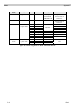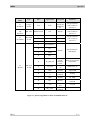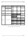
1
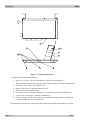
16-30 Watt Ku-Band BUC
High Power Transmitter Module
Operation and Maintenance Manual
This page has been intentionally left blank.
Mitec telecom inc.
Designers and manufacturers of telecom and wireless products
3299 Jean-Baptiste-Deschamps
Lachine, QC, H8T 3E4
Canada
OPERATION AND MAINTENANCE MANUAL
Preliminary
Released
REVISION RECORD
Revision
ECN #
Description
Date
0
Engineering Release.
22 Jul 05
1
Revised for all configurations
07 Nov 06
2
Revised to include expanded low frequency option
15 Nov 06
3
Revision for extended band 30W
20 Apr 07
4
Updated Appendix B
26 Mar 08
5
Changed the title to make it more generic
09 May, 08
6
30Watt Extended band option is removed.
09 Sep, 08
7
Updated to include -33 and -37
16 Oct, 08
8
Updated to include –26
18 Feb, 09
CM Approval
Approved
TITLE:
16 to 30 Watt, 70 dB Gain, Ku Band
ODU High Power Transmitter
Module
This document contains information proprietary to Mitec telecom inc., or its affiliates, or to a third party to which Mitec telecom inc. may have a legal obligation to protect
such information from unauthorized disclosure, use, or duplication. Any disclosure, use, or duplication of this document or of any of the information contained herein is
expressly prohibited except as Mitec telecom inc. may otherwise agree in writing.
Designer: Marina Lissianskaia
Date: 22 Jul 05
Technical Writer: Colleen Strunga Date: 22 Jul 05
REV 8
DOCUMENT NO.
20434-001MA
PAGE 1 OF 40
This page has been intentionally left blank.
mitec
Table of Contents
Table of Contents
1 INTRODUCTION ........................................................................... 1
1.1 Receiving and Inspection .........................................................................................2
1.1.1 Equipment Damage or Loss .............................................................................2
1.1.2 Return of Equipment ........................................................................................2
1.2 Preparing for Installation ........................................................................................3
1.2.1 Safety Precautions ............................................................................................3
2 INSTALLATION & OVERVIEW..................................................... 5
2.1 General Description .................................................................................................5
2.2 Specifications ............................................................................................................5
2.2.1 General Considerations ....................................................................................8
2.3 Basic Mechanical Characteristics ...........................................................................8
2.3.1 External View of the Transmitter Module........................................................8
2.3.2 Connections and Mounting Hardware..............................................................8
2.4 Assembly and Installation........................................................................................8
2.4.1 Lifting the Transmitter Module into Position and Temporary Attachment .....9
2.4.2 Securing the Transmitter Module.....................................................................9
2.5 Functional Overview ..............................................................................................10
2.5.1 General ...........................................................................................................10
2.5.2 IF/RF Conversion and Amplification.............................................................12
2.5.3 Monitor and Control (if applicable) ...............................................................12
2.5.4 Internal Power Distribution Reference...........................................................12
3 OPERATION ............................................................................... 13
3.1 Procedure ................................................................................................................13
3.2 Interface ..................................................................................................................14
4 MAINTENANCE .......................................................................... 15
4.1 Preventive Maintenance.........................................................................................15
Rev 8
i
Table of Contents
mitec
4.1.1
4.1.2
4.1.3
4.1.4
4.1.5
Procedure ........................................................................................................15
Transmitter Module Cooling System Preventive Maintenance......................15
Performance Check.........................................................................................17
Troubleshooting..............................................................................................17
Out-of Warranty Repair..................................................................................18
APPENDIX A ......................................................................................1
Drawings & Schematic Diagrams .................................................................................1
APPENDIX B ......................................................................................1
Serial Protocol.................................................................................................................1
APPENDIX C ......................................................................................1
Interface...........................................................................................................................1
APPENDIX D ......................................................................................1
Spare Parts ......................................................................................................................1
List of Tables
Table 1 –Specifications........................................................................................................6
Table 2 - Recommended Corrective Actions.....................................................................17
List of Figures
Figure 1 – Recommended Distance for Mounting on the Hub..........................................10
Figure 2 - System Block Diagram for –25, -33, -35 ..........................................................11
Figure 3 - System Block Diagram -37 ...............................................................................11
Figure 4 – Cooling Fan Replacement ................................................................................16
Figure 5 – WTX-14014542_43_44-70-ES-xx Outline drawing..........................................3
Figure 6 - WTX-13714542_43_44-70-ES-xx Outline drawing ..........................................4
Figure 7 - WTX-14014545-70-ES-37 Outline drawing ......................................................5
Figure 8 - Pin out assignments for WTX-1XX145XX-70-ES-25 .......................................1
Figure 9 - Pin out assignments for WTX-1XX145XX-70-ES-26 .......................................1
Figure 10 - Pin out assignments for WTX-1XX145XX-70-ES-33 .....................................2
Figure 11 - pin out assignments for WTX-1XX145XX-70-EX-35 .....................................3
Figure 12 - Pin out assignments for WTX-1XX145XX-70-ES-37 .....................................4
ii
Rev 8
mitec
Preface
Preface
Scope
This document covers the installation, operation, and maintenance of the 16 to 30 Watt, 70 dB Gain,
Ku Band ODU High Power Transmitter Modules. It contains information intended for engineers,
technicians and operators working with the transmitter module.
This document covers the following model in the 16 to 30 Watt Ku Band family.
Model
Power Level
WTX-14014542-70-ES-xx
16 Watts
WTX-14014543-70-ES-xx
20 Watts
WTX-14014544-70-ES-xx
25 Watts
WTX-14014545-70-ES-xx
30 Watts
WTX-13714542-70-ES-xx
16 Watts
WTX-13714543-70-ES-xx
20 Watts
WTX-13714544-70-ES-xx
25 Watts
Note: -xx stands for configuration i.e. -25, -26, -33, -35, -37 etc.
Note: The 30W Extended Ku Band version not available for this size PA. For 30 Extended Ku Band
option see the 40 to 50 W Ku band BUC series.
To make inquiries, or to report errors of fact or omission in this document, please contact Mitec
telecom inc. at (514) 694-9000.
IMPORTANT
Important information concerning the operation and care of this product, as well as safety of
authorized operators is highlighted throughout this document by one of the following labels:
NOTE
Indicates a reminder, a special consideration, or additional
information that is important to know.
Rev 8
P-1
mitec
Table of Contents
CAUTION!
Identifies situations that have the potential to cause equipment
damage.
WARNING!!
Identifies hazardous situations that have the potential to cause
equipment damage as well as serious personal injury.
2
Rev 8
mitec
Introduction
1 Introduction
The 16 to 30 Watt, 70 dB Gain, Ku Band ODU High Power Transmitter Modules are highly
reliable, high quality, cost efficient stand-alone transmitter systems. The application for these
modules is Ku-Band VSAT communication in an outdoor environment. This line of superior
products, engineered using state of the art technology, is characterized by unparalleled durability
and dependability. The output operating frequency range is the standard Ku-Band of 14.0 GHz to
14.5 GHz or the low extended Ku-Band of 13.75 GHz to 14.5 GHz. However, optional operating
frequency ranges are also available to suite the customer’s specification. Refer to Table 1.
Rev 8
Page 1
mitec
Introduction
1.1
Receiving and Inspection
The transmitter module is designed to function outdoors and will arrive in a standard shipping
container. Immediately upon receipt of the transmitter module, check the Bill of Lading against
the actual equipment you have received. Inspect the shipping containers exteriors for visible
damage incurred during shipping.
CAUTION!
Handle the transmitter module with extreme care. Excessive shock
may damage transmitter module’s delicate internal components.
NOTE
Before unpacking the shipping containers, move them near to the
site where the system will be mounted. Ensure that the
containers are oriented correctly in accordance with the “This
Side UP ”labels. Carefully remove the transmitter module and
packing material from the shipping containers.
Using the supplied packing list, verify that all items have been received and undamaged during
shipment. Verify that all items are complete. If there are any omissions or evidence of improper
packaging, please notify Mitec telecom inc. immediately.
1.1.1 Equipment Damage or Loss
Mitec Telecom Inc. is not responsible for damage or loss of equipment during transit. For
further information, contact the responsible transport carrier.
When declaring equipment as damaged during transit, preserve the original shipping cartons to
facilitate inspection reporting.
1.1.2 Return of Equipment
When returning equipment to Mitec for repair or replacement:
1. Identify, in writing, the condition of the equipment,
2. Refer to the sales order, Purchase Order and the date the equipment was received.
Notify Mitec Sales Administration Department of the equipment condition and obtain a Return
Material Authorization (RMA) number and shipping instructions. Mitec will pay for the cost of
shipping the product to the customer after the repairs are completed.
Page 2
Rev 8
mitec
Introduction
NOTE
Do not return any equipment without an RMA number. This is
important for prompt, efficient handling of the returned
equipment and of the associated complaint.
1.2
Preparing for Installation
Before attempting to install or use the transmitter module, we recommend that you first
familiarize yourself with the product by reading through this manual. Understanding the
operation of the system will reduce the possibility of incorrect installation, thereby causing
damage or injury to yourself or others.
The transmitter module must be installed in accordance with the
conditions and recommendations contained in the following
sections.
When you are ready to begin your installation, use the information in Chapter 2 (Installation) as a
guide for making all the required electrical connections.
1.2.1
Safety Precautions
Carelessness or mishandling of the transmitter module may damage the unit causing serious
injury to yourself or others. Please adhere to the following:
WARNING!!
This unit is equipped with an AC power cord and plug. Do not
tamper with, or attempt to reconfigure, the cord or plug supplied
with the unit, as this can:
♦ result in personal injury
♦ void the warranty
♦ cause damage to the units or related equipment.
Rev 8
Page 3
This page has been intentionally left blank.
mitec
Installation & Overview
2 Installation & Overview
2.1
General Description
This section describes the installation and theory of operation of the transmitter module.
The module is a stand-alone Transmitter System powered from 24 VDC and 110/220 VAC power
sources. It will amplify an input signal from an L-Band RF source up to a power level of 16-2025 Watts CW in Ku-Band.
The Transmitter consists of a low power block up-converter (BUC) and a high power amplifier
(Booster.)
The Booster has control and protection functions and consists of these major sub-systems: the RF
Amplifier, and power supply and a cooling system. The amplifier section contains all the
necessary DC power conditioning circuitry for bias and sequencing of the RF amplifier devices as
well as a RS-485 monitor and control interface.
The module can be used as a stand-alone unit or in a redundant configuration.
2.2
Specifications
Table 1 summarizes the specifications of the 16 to 30 Watt, 70 dB Gain, Ku Band ODU High
Power Transmitter Modules. Where specifications differ between different frequency band
options, it is noted in the table below, where:
yy = power in dBm
xx = configuration
For mechanical specifications, refer to the outline drawings, Figure 4 and 5 in Appendix A.
Rev 8
Page 5
mitec
Installation & Overview
Table 1 –Specifications
RF Performance
Output Frequency
WTX-140145yy-70-ES-xx
WTX-137145yy-70-ES-xx
IF Frequency
WTX-140145yy-70-ES-xx
WTX-137145yy-70-ES-xx
LO Frequency
WTX-140145yy-70-ES-xx
WTX-137145yy-70-ES-xx
Reference Frequency
Small Signal Gain
Gain Flatness (small signal)
at 10 dB back-off
Gain Stability with power (expansion)
Output Power
WTX-14014542-70-ES-xx
WTX-13714542-70-ES-xx
WTX-14014543-70-ES-xx
WTX-13714543-70-ES-xx
WTX-14014544-70-ES-xx
WTX-13714544-70-ES-xx
WTX-14014545-70-ES-xx
Saturated Output Power
WTX-14014542-70-ES-xx
WTX-13714542-70-ES-xx
WTX-14014543-70-ES-xx
WTX-13714543-70-ES-xx
WTX-14014544-70-ES-xx
WTX-13714544-70-ES-xx
WTX-14014544-70-ES-xx
rd
3 Order Intermodulation (IMD-3)
Phase Noise
Source & Load VSWR
Input Return Loss (cold)
Output Return Loss
Page 6
Standard Ku-Band: 14.0 to 14.5 GHz
Low Extended Band: 13.75 to14.5 GHz
Standard Ku-Band: 950 to 1450 MHz
Low Extended Band: 950 to 1700 MHz
Standard Ku-Band:
13.05 MHz
Low Extended Ku-Band: 12.8 MHz
10 MHz External Reference;
(0 ± 5) dBm Input Power Level
70 dB, min over temperature
± 2.0 dB, typ. (±2.5 dB max) over full band
± 0.3 dB, p-p, max. over any 40 MHz
0.5 dB, max.
42.0 dBm (16 W), min at P1dB
42.0 dBm (16 W), min at P1dB
43.0 dBm (20 W), min at P1dB
43.0 dBm (20 W), min at P1dB
44.0 dBm (25 W), min at P1dB
44.0 dBm (25 W), min at P1dB
45.0 dBm (25 W), min at P1dB
43.0 dBm (20 W), typ. at PSAT
43.0 dBm (20 W), typ. at PSAT
44.0 dBm (25 W), typ. at PSAT
44.0 dBm (25 W), typ. at PSAT
45.0 dBm (30 W), typ. at PSAT
45.0 dBm (30 W), typ. at PSAT
46 dBm (40 W), typ. at PSAT
-30 dBc typ., two equal signals at 6 dB back off
from P1dB rated total; 4 MHz separation
-60 dBc/Hz, max. @300 Hz offset of the carrier
-70 dBc/Hz, max. @ 1 kHz offset of the carrier
-80 dBc/Hz, max. @ 10 kHz offset of the carrier
-90 dBc/Hz, max. @ 100 kHz offset of the
carrier
-100 dBc/Hz, max. @ 1 MHz offset of the
carrier
1.5:1 max (operational), infinite at any angle
without damage, unconditionally stable
-14 dB typ.
-16 dB max.
Rev 8
mitec
Installation & Overview
RF Performance
Spurious In-band
Spurious Out of Band
Harmonics
RF Monitor Port (optional)
Power Consumption
Controls
Gain
Mute In S/W
Mute In H/W
Over Temperature Shutdown
Indicators
RF Forward Power
RF Reverse Power
RF On
Over Temperature
Alarm Summary
Temperature Sensor
Power Supply
Input
Output
Cooling
Auxiliary
Efficiency
Design Technology
Mechanical Specifications
Package
Size (overall dimensions
Weight
Cooling
Exterior Surface Finish
Hardware
O-ring
Markings
1
2
3
4
5
6
Rev 8
-50 dBc, max @ P1dB
-60 dBc, max @ P1dB
-55 dBc, typ. @ P1dB
N/A
300 W nominal
N/A
Via RS-485
TTL high – muted
(82 –2/+3) C at case temperature, internally set
Via RS-485
N/A
N/A
Via RS-485
TTL high – operational (optional)
Via RS-485
110/220 VAC, 300W min.
N/A
Forced Air
12 VDC, 3.5 A (optional)
85% nominal
High frequency switching modules
Outdoor, weather resistant
13”x12”x8”
11.5 Kg (24 lb) typical
Forced Air
Painted off-white
Stainless Steel
Silicone
Labels permanent and legible
Mitec Part No & Revision Level
Serial No.
IF Input
RF Output
RS-485 or RS-232
AC Input
Page 7
mitec
Installation & Overview
Environmental
Temperature
Humidity
Altitude
Shock and Vibration
Drop
Reliability
MTBF (mean time between failures)
2.2.1
Operational
Storage
-40° to 55°C
-50°C to 85°C
5% to 95% at –40°C 5% to 95% at 65°C
10,000 ft AMSL
40,000 ft AMSL
Normal transport and handling
N/A
1m in shipping container
100,000 hours (fan reliability data is not included.
Fan must be replaced once every 2 years
minimum.
General Considerations
The module shall meet all specifications over full bandwidth and under all environmental
conditions when terminated with a load of VSWR at 1.5:1 unless otherwise specified. All RF
specifications shall be met within five minutes after applying DC power, except gain flatness,
which shall be met after a warm-up period of ten minutes. During the warm-up period, the
module shall not exhibit any alarm or require an RF mute input signal to reset any alarm/fault
latches.
2.3
Basic Mechanical Characteristics
2.3.1
External View of the Transmitter Module
The physical external dimensions of the transmitter module are shown in and Table 1. All inputs
and outputs are shown in and described in Appendix C.
2.3.2
Connections and Mounting Hardware
The IF input connection requires a coaxial cable with an N-type male connector for the IF Input.
The RF output requires a waveguide with a WR75 flat flange. An O-ring shall be used to seal the
waveguide connection. There are also two cylindrical connectors on the RF Input side of the RF
amplifier for AC power and M&C interface. The pin assignments for these connectors are shown
in section 3. Two sets of U-bolts (2 per set) and corresponding nuts are shipped with the
transmitter to fasten it to the antenna boom. The customer should choose the appropriate U-bolt
set, depending on the shape of the antenna boom. See Figure 4 or 5 in Appendix A. Four cap
screws (#6-32) and their respective lock washers fasten the antenna waveguide feeder on to the
transmitter waveguide output flange. The mating connectors, hardware and O-ring are in the
shipping container with the transmitter.
2.4
Assembly and Installation
Use the information in this section as a guide to assemble and install the transmitter module. The
specified humidity is up to 100% during operation. However, installation should be carried out in
dry conditions, free of salt spray or excessive humidity. This will eliminate the possibility of
moisture and other foreign substances from entering the output waveguide flange.
Page 8
Rev 8
mitec
Installation & Overview
CAUTION!
Only authorized technical personnel should perform the
Installation and proper electrical hookups of the transmitter
module.
2.4.1
Lifting the Transmitter Module into Position and Temporary Attachment
The transmitter module weighs approximately 11.5kg (24 lb), which may require handling by a
two persons. Remove all plastic caps from the connectors and output waveguide flange. Lift the
transmitter module and install it on to the mounting frame opening. The transmitter module is
now ready for permanent attachment.
The transmitter is designed to operate in an outdoor environment and is waterproof when
mounted in the correct orientation as per Figure 1 and the orientation labels placed on the RF
amplifier shroud.
The transmitter contains a high flow-rate fans (300 CFM) for cooling the RF amplifier module.
These fans function continuously during the transmitter operation. To provide a sufficient
airflow, the transmitter should be mounted with a minimum clearance of 3 inches on all four sides
and the bottom. Refer to Figure 1. Adequate cooling for the transmitter will provide years of top
performance.
2.4.2
Securing the Transmitter Module
Secure the transmitter module on to the mounting frame using the hardware described in section
2.3.2. Align the transmitter output waveguide flange with the mating flange of the antenna feeder
waveguide.Using the O-ring and hardware provided, connect the antenna feeder waveguide.
Torque the flange screws to 16 inch-pounds (1.8 N-m). Attach the proper cables for waveguide
for IF input, AC power and M&C to the corresponding connectors of the transmitter module.
Refer to the model drawing in Appendix A.
Rev 8
Page 9
mitec
Installation & Overview
NOTE
The cylindrical connectors are labeled clearly and have different
pin layouts. Refer to pin out assignments in Appendix C . It is
impossible to incorrectly install the mating connectors.
Figure 1 – Recommended Distance for Mounting on the Hub
2.5
Functional Overview
2.5.1
General
This section describes the transmitter module functions in detail. The functional overview
explains the RF amplification, monitor & control and power distribution.
Figure 2 block diagram illustrates the transmitter module.
Page 10
Rev 8
mitec
Installation & Overview
RS-485
12V DC
Alarm
IF In
L-Band &
10MHz reference
(0 +/- 5 dBm)
with 24VDC
BUC &
SSPA
RF Out
12 VDc
Cooling System
2 fans
12 VDC
3 A max
AC Power In
Power Supply
Figure 2 - System Block Diagram for –25, -33, -35
RS-485
12V DC
Alarm
IF In
L-Band
Bias T
10MHz
reference
(0 +/- 5 dBm)
with 24VDC
BUC &
SSPA
12 VDc
RF Out
12 VDc
Cooling System
2 fans
12 VDC
3 A max
AC Power In
Power Supply
Figure 3 - System Block Diagram -37
Rev 8
Page 11
mitec
Installation & Overview
2.5.2
IF/RF Conversion and Amplification
The IF Input signal with a 10MHz reference, 0±5dBm and 24VDC, 1.0A nominal enters the BUC
by a coaxial cable, converted to Ku-Band by the BUC and goes through an isolator, which
provides a good VSWR at the input. Under normal operation, the RF amplifier will amplify the
RF Input signal level up to a power level of 42 to 45 dBm (16 to 30 Watts CW) P1dB minimum.
For small signal gain, the transmitter module is capable of providing a gain of approximately 70
dB.
To achieve the rated output power, GaAs transistors, as well as other microwave components
within the RF Amplifier, provide the necessary gain and low insertion loss. The amplified signal
is transmitted through the output waveguide section to a satellite up-link system.
2.5.3
Monitor and Control (if applicable)
The transmitter has an RS-485 serial interface. The transmitter can communicate to the indoor
unit or redundancy control module via RS-485. RS-485 Protocol Specifications are found in
Appendix B, if applicable.
The control system can provide the following M&C functions:
System Alarm: when an amplifier is not functioning properly, TTL logic will activate an
alarm (TTL high: alarm condition). The alarm signal will be transmitted via RS-485 as
well as through two analogue wires in order to support the redundancy option.
Mute Control (via RS-485)
Mute Control (via hardware line): TTL high level signal will mute a transmitter
Output Power Monitoring: 15 dB dynamic range (via RS-485)
Base Plate Temperature Monitoring (via RS-485)
The SSPA can also provide 12VDC (2A max) at the same connector to supply DC power for
redundancy control.
2.5.4
Internal Power Distribution Reference
The SSPA operates from power source of 110/220 VAC, 50 Hz to 60 Hz and will consume
1,200-Watts maximum.
CAUTION!
There is an internal slow blowing fuse installed in the power
supply module in order to protect the entire system from over
current.
The power supply converts the incoming AC voltage into two separate DC voltages. The
DC voltages are regulated to ensure isolation and stability.
Page 12
Rev 8
mitec
Maintenance
3
Operation
This chapter describes the verification of the operation and control of the transmitter module. It
shall be performed by authorized personnel prior to maintenance and/or repair.
3.1
Procedure
Verify that the installation procedure described in Chapter 2 was completed. A complete physical
check of the customer’s system is suggested.
WARNING!
The output power available at the output waveguide flange is
extremely hazardous. Under no circumstances should be
transmitter be operated without the waveguide feed or a high
power load attached. Do not operate this equipment in the
presence of flammable gases or fumes. Failure to observe this
precaution will result in personal injury. Safe and careful
installation of this transmitter will eliminate the possibility of
accidents and provide years of top performance.
Verify the antenna feed waveguide connection is properly done before the transmitter is
energized.
NOTE
The transmitter module can withstand any source or load VSWR.
However, the transmitter module will meet all specification
requirements only if the source/load VSWR is sufficient. Refer to
Section 2.2
Normal operation is not possible if the antenna feeder VSWR is
greater than 1.5:1.
Turn ON the power and allow a warm up period of twenty minutes before operating the
transmitter module. This will assure stable gain and power. The transmitter module can function
with a coupler when a direct measurement of the output power is made.
Rev 8
Page 13
mitec
Maintenance
CAUTION!
It is strongly recommended not to exceed -20 dBm maximum RF
Input level. The RF amplifier will be in deep saturation if
overdriven. RF performance will degrade significantly, and proper
operation is not possible. This operational condition is the survival
mode for the transmitter module. Never exceed the maximum safe
RIF Input level of -10dBm (100 mW) or permanent damage to the
transmitter module may result.
Verify the status of the System Fail signal from the M&C interface using the RS-485 protocol.
(Protocol description is attached to this manual.)
3.2
Interface
The connector interface is described in Appendix C. The serial interface, if applicable, is
documented in Appendix B.
Page 14
Rev 8
mitec
Maintenance
4 Maintenance
This chapter contains information on how to maintain, troubleshoot and repair the transmitter
module. The transmitter module is extremely reliable, requiring very little preventive
maintenance, or repair. Should there be a malfunction, this chapter also contains technical
information to help diagnose basic failures.
4.1
Preventive Maintenance
4.1.1
Procedure
WARNING!
Shut down the transmitter module before disassembly and
remove all cables and connectors. Failure to observe this
precaution may result in personal injury or death. This includes
the removal of any RF power originating from other system
components.
When the transmitter module is in the hot stand-by mode in a redundant system, switch it to the
operation mode at least once every three months. Make sure the fan is running while in operation
mode.
When the transmitter module is in the cold stand-by mode in a redundant system, switch it to the
operation mode at least once every three months. Make sure the fan is running while in operation
mode.
4.1.2
Transmitter Module Cooling System Preventive Maintenance
Preventive maintenance is limited to checking the performance of the transmitter module cooling
system. No electrical or mechanical adjustments are required for normal operation.
The fan is the least reliable item in the transmitter module. Wearing of the fan bearings will
cause the RPM to drop and will create a higher than average heat-sink temperature. It is
recommended to replace the fan after 2 years of operation.
The Cooling system was designed so that the fan can be replaced easily in the field. Refer to
Figure 4 below.
Rev 8
Page 15
mitec
Maintenance
4
3
5 6
7
1 2
8
Figure 4 – Cooling Fan Replacement
To replace the fan, perform the following:
1.
2.
3.
4.
5.
6.
7.
8.
Remove six screws (1) and six lockwashers (2) from the bottom shroud (3)
Remove bottom shroud (3) with attached fan (7) and fan holder (8) from the transmitter (4)
Disconnect wires of fan (7) to transmitter (4)
Remove four screws (5) and four lockwashers (6)
Remove fan (7) from fan holder (8)
Using four screws (5) and four lockwashers (6), install new fan (7) onto fan holder (8)
Connect wires of new fan (7) onto the transmitter (4).
Using six screws (1) and six lockwashers (2), reinstall the bottom shroud (3) with the fan
(7) and fan holder (8) on to transmitter (4).
The transmitter module is now ready for operation and no other periodic maintenance is required.
Page 16
Rev 8
mitec
4.1.3
Maintenance
Performance Check
Verify the system is properly set up as per Chapters 2 and 3. The power output at 1dB
compression shall be measured for evaluating the performance of the transmitter module.
It is recommended to measure the following parameters for ensuring that the transmitter module
is in good working condition:
- Gain and Gain flatness
- RF load VSWR and RF source VSWR
- Two-Tone Intermodulation Distortion
- Return Loss at connectors J1 and J2 of the TRANSMITTER MODULE
Using a Source and an IF input signal level within the small signal region of the transmitter
module, measure the power level at connectors J1 and J2. See Figure 4. Plot the swept response
on a test data sheet. From the plot, determine gain and gain flatness.
With an IF Input signal level within the small signal region of the transmitter module, measure
the VSWR (Return Loss) at connectors J1 and J2. See Figure 4. Plot the swept return loss for
both the IF Input and RF Output signals on a test data sheet. From the plot determine the return
loss.
From the output power measurements determine P1dB. Record value on a test data sheet.
Measure the Two-tone Intermodulation Suppression using two equal signals separated by 5 MHz.
Record value on test data sheet.
4.1.4
Troubleshooting
WARNING!!
Cable connection and disconnection shall be done carefully to
avoid physical damage to the cables and connectors, which may
cause intermittent problems in the future.
Use Table 1 to quickly isolate a fault within the transmitter module. If the transmitter module is
defective, notify Mitec and follow the process detailed in section 1.1.2.
Symptom
Action
Fails performance test
Check power source, RF source, cabling and connectors. Check
for clogged fan and debris in heat-sink fins. Clean thoroughly.
If fan is worn, replace fan. If correct, transmitter module is
defective. Return transmitter module to Mitec.
Table 2 - Recommended Corrective Actions
Rev 8
Page 17
mitec
Maintenance
4.1.5
Out-of Warranty Repair
A non-warranty and out-of-warranty repair service is available from Mitec for a nominal charge.
The customer is responsible for paying the cost of shipping the SSPA both to and from Mitec for
these repairs.
Page 18
Rev 8
mitec
Appendix A
Appendix A
Drawings & Schematic Diagrams
16 to 30 Watt, 70 dB Gain, Ku Band ODU High Power Transmitter Module - Outline Drawings
Rev 8
A-1
This page has been intentionally left blank.
mitec
Appendix A
13.11
2.50
48 VDC
7.51 ¢
3.88
J3
0.41 x 1.00
SLOT
(4 PL.)
LABELING VARY, DEPENDING ON PART LIST
REF VIEW
0.55
12.18
14.00
N CONN COVER
10.28
¢
¢
ku BAND BUC
1.98
IF IN
J1
IF IN
N CONN
(FEMALE)
RF IN
M&C
GUARA NTEE
VOID IF SEAL
BROK EN
1.14
J4
RF OUT
J2
INTERFACE
CONN
RF OUT
WR75G
11.88
J3
AC POWER IN
110/220 VAC
POWER IN
CONN
P/N : MD -WTX-1401454X-70-ES-XX
SER. NO : XX XXXXXXX
REV: (X)
D/C: (YY/ WK)
mitec telecom inc.
MADE IN CANADA
CONN COVER
SUPPLIED WITH CONN
LABEL ID LOCATION
WR75G CAP DUST
Figure 5 – WTX-14014542_43_44-70-ES-xx Outline drawing
Rev 8
A-3
This page has been intentionally left blank.
mitec
Appen
Figure 6 - WTX-13714542_43_44-70-ES-xx Outline drawing
C- 4
Rev 8
This page has been intentionally left blank.
mitec
Appendix A
Figure 7 - WTX-14014545-70-ES-37 Outline drawing
Rev 8
A-5
This page has been intentionally left blank.
mitec
Appendix B
Appendix B
Serial Protocol
Appendix B contains information of the RS-485 Serial Protocol, if applicable.
Rev 8
B-1
This page has been intentionally left blank.
9000 Trans Canada, Pointe Claire, QC, Canada H9R 5Z8
Confidential and Proprietary to Mitec. This is a Controlled Document.
Document Name:
Protocol Specification
Revision:
01
File Name:
PS-3900040-00-R01
Page:
Page 1 of 14
Model Number:
N/A
Originator:
R. Abdouche
Revision
0A
0B
0C
0D
0E
Date
22-Apr-2003
01
10-May-2007
04-Dec-2003
16-Jan-04
Change Summary
Preliminary specification sent to customer.
Document does not exist.
Document does not exist.
Extracted protocol specs from technical specs document.
Completely revamped the document format. No functional
changes made.
Added attenuation control command.
Approval
C. Villeneuve
C. Villeneuve
C. Villeneuve
C. Villeneuve
Serial Communication Protocol Specification
For
Control Software 3900040-00
Table of Contents
1
Document legend_____________________________________________________________ 3
2
Project Overview _____________________________________________________________ 3
3
Definitions and acronyms______________________________________________________ 3
4
Scope ______________________________________________________________________ 3
5
Serial Communications Link Interface ___________________________________________ 4
6
5.1
Customer Interface Port Configuration _____________________________________________4
5.2
Customer Interface Cable Connections ______________________________________________4
Communication Protocol Framing ______________________________________________ 6
6.1
6.1.1
6.1.2
6.1.3
6.1.4
7
8
SCI Packet Frame Format ________________________________________________________6
SCI Packet Byte Description ___________________________________________________________
Default Address Values _______________________________________________________________
CRC Calculation Example_____________________________________________________________
Command / Reply Packet Sequencing____________________________________________________
6
7
7
7
Command List _______________________________________________________________ 8
7.1
Default Reply Packet Format ______________________________________________________8
7.2
GET Status Command List________________________________________________________9
7.3
GET Alarms Command List______________________________________________________11
7.4
SET Control Command List______________________________________________________12
Appendix I: Troubleshooting Guide_____________________________________________ 13
PS-3900040-00-R01
Designed: R. Abdouche
Approved: C. Villeneuve
Rev. 01
Page 2 of 14
11-05-07 10:06 AM
1
Document legend
Text in this document highlighted in grey identifies features which are planned but not implemented yet.
2
Project Overview
This document describes the communications protocol used to communicate with high-power transmitter modules
(ODUs) configured with embedded software 3900040-00 when used in a stand-alone configuration.
Customer PC / Modem
WTX Interface
Booster
(ex. Address = 0xF)
Figure 1) System Block Diagram
If the Booster is configured in a redundant configuration, then the communications protocol for the redundant kit
supercedes the present document.
3
Definitions and acronyms
The following terms appear throughout this document:
Controller:
CRC:
Customer Interface Port:
Customer Interface Device:
PC:
RF:
SCI:
WBT:
WTX:
4
The microprocessor-based card and associated embedded software which
handles all communications between the customer interface and the
amplifier.
Cyclic Redundancy Check
The interface port through which the device used by the customer will
interact with the Transceiver (ie. typically a modem or PC).
The interface device used by the customer to interact with the Transceiver
(ie. typically a modem or PC).
Personal Computer.
Radio Frequency.
Serial Communications Interface.
Wavesat Bias Tee Unit
Wavesat Transmitter
Scope
This document covers all aspects of the communication protocol which are required for the customer to develop a
controlling device (typically a PC application program or modem) to interface with the Mitec product.
PS-3900040-00-R01
Designed: R. Abdouche
Approved: C. Villeneuve
Rev. 01
Page 3 of 14
11-05-07 10:06 AM
5
5.1
Serial Communications Link Interface
Customer Interface Port Configuration
The customer interface port of the controller is configured as follows:
Baud Rate:
19200bps
Data bits:
8
Stop bits:
1
Parity:
None
HW Control
None
5.2
Customer Interface Cable Connections
This software protocol remains the same regardless of the transport medium used (ie RS232, RS485 half duplex
or RS485 full duplex). This section defines the wiring required to communicate with the Mitec product.
Note that the pin numbers on both side of the cable are deliberately omitted since these will vary depending on
the Mitec product as well as the PC / Modem interface. Please refer to the specific user manuals for pin
allocations.
Please refer to the user manual for the Mitec product if unsure of the customer interface transport medium.
For RS232:
PC / Modem
Interface
TX
RX
RX
TX
Gnd
Gnd
Transceiver
Customer
Interface
Note: Some PC com ports require that loopbacks be present at the PC / modem interface. If
such is the case, then connect the following signals together at the PC / modem interface:
Interconnect: "DTE Ready" to "DCE Ready" to "Received Line Signal Detect".
Also interconnect: "Request to Send" to "Clear to Send"
Also note that this diagram only represents the serial communication connections. Refer to
the user manual for any other signals which may be provided through this interface.
Figure 2) RS232 Customer Interface Wiring
PS-3900040-00-R01
Designed: R. Abdouche
Approved: C. Villeneuve
Rev. 01
Page 4 of 14
11-05-07 10:06 AM
For RS485 Half Duplex:
Data+
TX+
RX+
PC / Modem
Interface
Data-
TXRX-
Gnd
Transceiver
Customer
Interface
Gnd
Note: Some PC cards provide TX+, RX+, TX- and RX- hardware signals
instead of Data+ and Data-. In this case, the TX+ and RX+ lines are to be
shorted together to form the Data+ signal. Similarly, the TX- and RX- lines
are to be shorted together to form the Data- signal.
Also note that this diagram only represents the serial communication
connections. Refer to the user manual for any other signals which may be
provided through this interface.
Figure 3) RS485 Half Duplex Customer Interface Wiring
For RS485 Full Duplex (ie RS422):
PC / Modem
Interface
RX+
TX+
TX+
RX+
RX-
TX-
TX-
RX-
Gnd
Gnd
Transceiver
Customer
Interface
Note that this diagram only represents the serial communication
connections. Refer to the user manual for any other signals which may be
provided through this interface.
Figure 4) RS485 Full Duplex (ie RS422) Customer Interface Wiring
PS-3900040-00-R01
Designed: R. Abdouche
Approved: C. Villeneuve
Rev. 01
Page 5 of 14
11-05-07 10:06 AM
6
Communication Protocol Framing
6.1
SCI Packet Frame Format
The packets exchanged with the master controller will have the following format (regardless of direction):
Packet Frame Format:
MSB
STX
LSB
Dest/Src
Address
Cmd/Len
Data
CRC
MSB
Data Format:
Data1
ETX
LSB
Data2
Datan-1
Datan
Figure 5) SCI Packet Frame Format
6.1.1
SCI Packet Byte Description
♦
STX is the start transmission byte (defined as 0x7E). This byte is used to determine the start of a packet.
♦
Dest/Src Address contains the destination address in the high nibble and the source address in the low
nibble. The destination address is the address of the device which is to process the packet. The source
address is the address of the device which sent the packet. Note that the device address of the customer
interface device is always = 0x0F.
♦
CMD/Len contains the packet command in the high nibble and the number of bytes in the data portion of
the packet in the lower nibble.
The following commands may be sent by the customer interface device:
GET (command high nibble = 0x0)
Request the current value of a database element.
SET (command high nibble = 0x1)
Set the database element to the specified value.
The following commands may be returned to the customer interface device:
UPD (command high nibble = 0x8)
Return the current value of a database element.
ACK (command high nibble = 0xE)
Acknowledge a received packet.
NACK (command high nibble = 0xF)
Reject a received packet (Not ACKnowledge).
♦
Data1 - Datan contains the packet payload. The value of the data bytes is specific to the command and will be
covered in following sections.
♦
CRC is the cyclic redundancy check and is calculated by performing a byte-wise exclusive OR of the
Dest/Src address byte, Cmd/Len byte and all data bytes. A bit-wise inversion is then applied to the CRC
before being inserted into the packet.
♦
ETX is the end transmission byte (defined as 0x7F). This byte is used to determine the end of a packet.
PS-3900040-00-R01
Designed: R. Abdouche
Approved: C. Villeneuve
Rev. 01
Page 6 of 14
11-05-07 10:06 AM
6.1.2
Default Address Values
The customer interface device must always be assigned address 0xF.
The Booster device address is factory defaulted to 0xF. It may be set by the customer using the SET Booster Address
command (refer to SET Control Command List).
6.1.3
CRC Calculation Example
To send a command to read the temperature (database element =
0x0606) from the Booster (device address 0x0F), the command is:
7E
FF
02
06
06
02
Dest/Src = 0xFF
1111 1111
CMD/Len = 0x02
0000 0010
7F
XOR
= 1111 1101
XOR
Data1 = 0x06
0000 0110
= 1111 1011
XOR
Data2 = 0x06
0000 0110
= 1111 1101
Perform bitwise
inversion of final result:
6.1.4
= 0000 0010
= 0x02
CRC
Command / Reply Packet Sequencing
The Booster will never send a packet to the customer interface device unless a command is received. In other words, the
Booster will not speak unless spoken to.
PS-3900040-00-R01
Designed: R. Abdouche
Approved: C. Villeneuve
Rev. 01
Page 7 of 14
11-05-07 10:06 AM
7
7.1
Command List
Default Reply Packet Format
This section identifies the packet format the ACK (Acknowledge) and NACK (Not acknowledge) replies which may be sent to the customer interface device in
response to a received command.
NOTE: The packets shown in the list below are based on the assumption that the Booster device address is set to 0xF. To modify the commands for different
addresses, the Dest/Src byte and the CRC byte will have to change in all packets.
Reply
ACK (Acknowledge)
Packet Format
7E FX E0 ZZ 7F
Explanation
Acknowledge that the received packet was
properly processed.
NACK (Not Acknowledge)
7E FX F1 YY ZZ 7F
Indicate that a problem was encountered with
the received packet.
Interpretation
X = Device address of the packet
source device.
ZZ = CRC.
X = Device address of the packet
source device.
YY = Error code
(03 = Incorrect CRC
18 = Unrecognized command
30 = Set command attempted on a
restricted database element)
Examples
1) reply: 7E FF E0 E0 7F
(ACK reply sent from the Booster)
1) reply: 7E FF F1 03 F2 7F
(NACK reply sent from the Booster for an
invalid CRC)
2) reply: 7E FF F1 18 E9 7F
(NACK reply sent from the Booster for an
unrecognized command).
ZZ = CRC.
PS-3900040-00-R01
Designed: R. Abdouche
Approved: C. Villeneuve
Rev. 01
Page 8 of 14
11-05-07 10:06 AM
7.2
GET Status Command List
This section identifies the list of commands available to query any unit for status information.
NOTE: The packets shown in the list below are based on the assumption that the Booster device address is set to 0xF. To modify the commands for different
addresses, the Dest/Src byte and the CRC byte will have to change in all packets.
Command
Get Booster Temperature
Packet Format
7E FF 02 06 06 02 7F
Explanation
Query booster for
current temperature
Possible Replies
Update Booster Temp:
Interpretation
TT TT = Booster temp in oC + 273.
ZZ = CRC.
7E FF 84 06 06 TT TT ZZ 7F
NACK
Get Booster Temperature
Sensor Voltage
Get Booster Output Power
7E FF 02 2F FF D2 7F
7E FF 02 17 FF EA 7F
Query booster for
current temperature
sensor voltage (Note:
This command is to be
used if a more accurate
temperature reading is
required than the result
of the “Get Booster
Temperature”
command.)
Query booster for
current output power
Update Booster Temp
Sensor:
Refer to 7.1.
VV VV = Booster temp sensor
voltage from 0V (0x0000) to +5V
(0x03FF).
7E FF 84 2F FF VV VV ZZ 7F
The conversion formula is:
Temp = (Voltage x 0.4883) – 273.
ZZ = CRC.
NACK
Update Booster Output
Power:
Refer to 7.1.
PP PP = Output power in 10 x
dBm.
ZZ = CRC.
7E FF 84 17 FF PP PP ZZ 7F
PS-3900040-00-R01
Designed: R. Abdouche
Approved: C. Villeneuve
7E FF 02 18 FF E5 7F
Query booster for
current gain
2) cmd: 7E FF 02 06 06 02 7F
reply: 7E FF 84 06 06 01 34 B1 7F
(Temp = 0x0134 = 0d308 – 273 =
+35oC)
1) cmd: 7E FF 02 2F FF D2 7F
reply: 7E FF 84 2F FF 02 06 50 7F
(Voltage = 0x0206 = 0d518.
Temp = (518 x 0.4883) – 273 =
-20.1oC)
2) cmd: 7E FF 02 2F FF D2 7F
reply: 7E FF 84 2F FF 02 76 20 7F
(Voltage = 0x0276 = 0d630.
Temp = (630 x 0.4883) – 273 =
+34.6oC)
1) cmd: 7E FF 02 17 FF EA 7F
reply: 7E FF 84 17 FF 01 2C 41 7F
(Power = 0x012C = 0d300 =
30.0dBm.)
7E FF 84 18 FF GG GG ZZ 7F
2) cmd: 7E FF 02 17 FF EA 7F
reply: 7E FF 84 17 FF 01 A0 CD 7F
(Power = 0x01A0 = 0d416 =
41.6dBm.)
1) cmd: 7E FF 02 18 FF E5 7F
reply: 7E FF 84 18 FF 02 08 69 7F
(Gain = 0x0208 = 0d520 = 52.0dB.)
NACK
2) cmd: 7E FF 02 18 FF E5 7F
reply: 7E FF 84 18 FF 01 95 F7 7F
(Gain = 0x0195 = 0d405 = 40.5dB.)
NACK
Get Booster Gain (if
applicable)
Examples
1) cmd: 7E FF 02 06 06 02 7F
reply: 7E FF 84 06 06 01 02 87 7F
(Temp = 0x0102 = 0d258 – 273 =
-15oC)
Update Booster Gain:
Refer to 7.1.
GG GG = Gain in 10 x dB.
ZZ = CRC.
Refer to 7.1.
Rev. 01
Page 9 of 14
11-05-07 10:06 AM
Command
Get Mute Status
Packet Format
7E FF 02 06 01 05 7F
Explanation
Query booster for
mute status
Possible Replies
Update Mute Status:
7E FF 84 06 01 00 MM ZZ 7F
Interpretation
MM = Mute status (0 = enabled; 1
= muted)
ZZ = CRC.
Examples
1) cmd: 7E FF 02 06 01 05 7F
reply: 7E FF 84 06 01 00 00 83 7F
(Booster is enabled.)
2) cmd: 7E FF 02 06 01 05 7F
reply: 7E FF 84 06 01 00 01 82 7F
(Booster is muted.)
Get IF Frequency
Get Booster SW Version
Base number (MSB)
Get Booster SW Version
Base number (LSB)
Get Booster SW Version
Configuration
Get Booster SW Version
Revision
7E FF 02 16 FF EB 7F
7E FF 02 05 FC FB 7F
7E FF 02 05 FD FA 7F
7E FF 02 05 FE F9 7F
7E FF 02 05 FF F8 7F
Query transceiver for
IF frequency
NACK
Update IF Frequency:
Query booster for SW
version base MSB
7E FF 84 16 FF XX XX ZZ 7F
NACK
Update SW Version Base
MSB:
Query booster for SW
version base LSB
7E FF 84 05 FC 39 00 44 7F
NACK
Update SW Version Base
LSB:
Query booster for SW
version configuration
Query booster for SW
version revision
7E FF 84 05 FD XX XX ZZ 7F
NACK
Update SW Version Config:
7E FF 84 05 FE 00 XX ZZ 7F
NACK
Update SW Version revision:
7E FF 84 05 FF RR RR ZZ 7F
Get Booster Device Address
7E FF 02 03 04 05 7F
Query booster for
device address
NACK
Update booster device
address:
7E FF 84 03 04 00 XX ZZ 7F
NACK
Get Attenuation Setting
(if applicable)
7E FF 02 03 07 06 7F
Query booster for
attenuation setting
Update Attenuation Setting:
7E FF 84 03 07 00 XX ZZ 7F
NACK
PS-3900040-00-R01
Designed: R. Abdouche
Approved: C. Villeneuve
Refer to 7.1.
XX XX = System IF frequency in
MHz.
ZZ = CRC.
Refer to 7.1.
SW version base number MSB is
always 0x3900.
Refer to 7.1.
XX XX = SW version base number
(LSB).
ZZ = CRC.
Refer to 7.1.
XX = SW version configuration.
ZZ = CRC.
Refer to 7.1.
RR RR = SW version revision
represented as two ASCII
characters.
ZZ = CRC.
Refer to 7.1.
XX = Booster device address.
ZZ = CRC.
Refer to 7.1.
XX = Attenuation in 0.1 dB.
ZZ = CRC.
Refer to 7.1.
1) cmd: 7E FF 02 16 FF EB 7F
reply: 7E FF 84 16 FF 03 B6 D8 7F
(IF frequency set to 0x03B6 = 0d950
= 950 MHz)
1) cmd: 7E FF 02 05 FC FB 7F
reply: 7E FF 84 05 FC 39 00 44 7F
cmd: 7E FF 02 05 FD FA 7F
reply: 7E FF 84 05 FD 00 40 3C 7F
cmd: 7E FF 02 05 FE F9 7F
reply: 7E FF 84 05 FE 00 00 7F 7F
cmd: 7E FF 02 05 FF F8 7F
reply: 7E FF 84 05 FF 30 31 7F 7F
The resulting software version is:
3900040-00-R01
1) cmd: 7E FF 02 03 04 05 7F
reply: 7E FF 84 03 04 00 0A 89 7F
(Booster device address = 0xA)
2) cmd: 7E FF 02 03 04 05 7F
reply: 7E FF 84 03 04 00 FF 7C 7F
(Booster device address = 0xF)
1) cmd: 7E FF 02 03 07 06 7F
reply: 7E FF 84 03 07 00 64 E4 7F
(Attenuation set to 0x64 = 0d100 =
10.0 dB)
Rev. 01
Page 10 of 14
11-05-07 10:06 AM
7.3
GET Alarms Command List
This section identifies the list of commands available to query any unit for alarm information.
NOTE: The packets shown in the list below are based on the assumption that the Booster device address is set to 0xF. To modify the commands for different
addresses, the Dest/Src byte and the CRC byte will have to change in all packets.
Command
Get Booster Over
Temperature Alarm
Packet Format
7E FF 02 00 02 00 7F
Explanation
Query booster for over
temperature alarm
Possible Replies
Update booster over
temperature alarm:
7E FF 84 00 02 00 XX ZZ 7F
NACK
Get Booster Low Power
Alarm (if applicable)
7E FF 02 00 05 07 7F
Query booster for low
power alarm
Update booster low power
alarm:
7E FF 84 00 05 00 XX ZZ 7F
NACK
Get Booster Summary
Alarm
7E FF 02 00 0F 0D 7F
Query booster for
summary alarm
Update booster summary
alarm:
7E FF 84 00 0F 00 XX ZZ 7F
NACK
PS-3900040-00-R01
Designed: R. Abdouche
Approved: C. Villeneuve
Interpretation
XX = Alarm state (0x00 = no
alarm; 0x11 = alarm)
ZZ = CRC.
Examples
1) cmd: 7E FF 02 00 02 00 7F
reply: 7E FF 84 00 02 00 11 97 7F
(Booster over temp alarm is raised)
Refer to 7.1.
2) cmd: 7E FF 02 00 02 00 7F
reply: 7E FF 84 00 02 00 00 86 7F
(Booster over temp alarm is clear)
1) cmd: 7E FF 02 00 05 07 7F
reply: 7E FF 84 00 05 00 11 90 7F
(Booster low power alarm is raised)
XX = Alarm state (0x00 = no
alarm; 0x11 = alarm)
ZZ = CRC.
Refer to 7.1.
XX = Alarm state (0 = no alarm; 1
= alarm)
ZZ = CRC.
Refer to 7.1.
2) cmd: 7E FF 02 00 05 07 7F
reply: 7E FF 84 00 05 00 00 81 7F
(Booster low power alarm is clear)
1) cmd: 7E FF 02 00 0F 0D 7F
reply: 7E FF 84 00 0F 00 01 8A 7F
(Booster summary alarm is raised)
2) cmd: 7E FF 02 00 0F 0D 7F
reply: 7E FF 84 00 0F 00 00 8B 7F
(Booster summary alarm is clear)
Rev. 01
Page 11 of 14
11-05-07 10:06 AM
7.4
SET Control Command List
This section identifies the list of commands available to set control parameters any unit.
NOTE: The packets shown in the list below are based on the assumption that the Booster device address is set to 0xF. To modify the commands for different
addresses, the Dest/Src byte and the CRC byte will have to change in all packets.
Command
Packet Format
Set Mute Control
7E FF 14 13 01 00 MM ZZ 7F
Explanation
Mute / Unmute the up link.
MM = Mute control (1 =
Mute; 0 = enable)
Possible
Replies
ACK
Interpretation
Refer to 7.1.
NACK
Refer to 7.1.
ACK
Refer to 7.1.
ZZ = CRC
Set IF Frequency
7E FF 14 16 FF XX XX ZZ 7F
Set up link frequency
XX XX = Frequency in MHz.
ZZ = CRC
Examples
1) cmd: 7E FF 14 13 01 00 01 07 7F
reply: ACK
(Mute up link)
2) cmd: 7E FF 14 13 01 00 00 06 7F
reply: ACK
(Enable up link)
1) cmd: 7E FF 14 16 FF 03 B6 48 7F
reply: ACK
(Set IF frequency to 950 MHz = 0x3B6)
2) cmd: 7E FF 14 16 FF 04 33 CA 7F
reply: ACK
(Set IF frequency to 1075 MHz = 0x433)
NACK
Refer to 7.1.
3) cmd: 7E FF 14 16 FF 04 B0 49 7F
reply: ACK
(Set IF frequency to 1200 MHz = 0x4B0)
4) cmd: 7E FF 14 16 FF 05 2D D5 7F
reply: ACK
(Set IF frequency to 1325 MHz = 0x52D)
Set Booster Device Address
Set Booster Attenuation
(if applicable)
7E FF 14 03 04 00 XX ZZ 7F
7E FF 14 03 07 00 XX ZZ 7F
Set booster device address
(0 ≤ address ≤ 0xE)
Set booster attenuation
XX = Attenuation to set in 0.1
dB (range from 0 to 20 dB)
ACK
Refer to 7.1.
NACK
Refer to 7.1.
ACK
Refer to 7.1.
NACK
Refer to 7.1.
ZZ = CRC
PS-3900040-00-R01
Designed: R. Abdouche
Approved: C. Villeneuve
5) cmd: 7E FF 14 16 FF 05 AA 52 7F
reply: ACK
(Set IF frequency to 1450 MHz = 0x5AA)
1) cmd: 7E FF 14 03 04 00 0A 19 7F
reply: ACK
(Set Booster device address to 0xA)
2) cmd: 7E FF 14 03 04 00 0E 1D 7F
reply: ACK
(Set Booster device address to 0xE)
1) cmd: 7E FF 14 03 07 00 00 10 7F
reply: ACK
(Set Booster attenuation to 0 dB)
2) cmd: 7E FF 14 03 07 00 9B 8B 7F
reply: ACK
(Set Booster attenuation to 0x9B = 0d155 =
15.5 dB)
Rev. 01
Page 12 of 14
11-05-07 10:06 AM
Appendix I: Troubleshooting Guide
Problem
No response at all from Booster
Reply packet is incomplete.
PS-3900040-00-R01
Designed: R. Abdouche
Approved: C. Villeneuve
Possible Remedies
1)
Ensure the cable assembly is wired properly (refer to 5.2Customer Interface Cable
Connections) and that it is properly connected between the transceiver customer interface
port and the customer device.
2)
Verify that the com port parameters are as specified in 5.1Customer Interface Port
Configuration.
3)
Confirm that the customer interface cable is connected to the correct PC com port.
4)
Ensure that there are no other applications executing on the same com port.
5)
If the transport medium is RS232, then connect the loopbacks identified in the note in Figure
2) RS232 Customer Interface Wiring.
6)
If using a Booster address other than 0xF, then send a “GET Booster Device Address”
command to destination address 0xF. The reply will contain the current booster address. Note
that the booster will respond to all commands received with destination address 0xF.
7)
If the transport medium is RS485 half duplex, note that some PC cards require software
control of the RS485 transmit and receive buffer enable lines. The software in the customer
device may need to coordinate the enabling /disabling of these buffers.
8)
1)
Ensure the booster is powered on.
If software control of the transmit and receive buffer enable lines is required (RS485 half
duplex), then it is possible that the timing between the transition needs to be adjusted.
Rev. 01
Page 13 of 14
11-05-07 10:06 AM
This page left intentionally blank.
PS-3900040-00-R01
Designed: R. Abdouche
Approved: C. Villeneuve
Rev. 01
Page 14 of 14
11-05-07 10:06 AM
mitec
Appendix C
Appendix C
Interface
Appendix C contains the interface for the unit that this manual accompanies.
Connector
Name
Type
Pin #
Signal Name
Description
Parameter
J1
“IF INPUT”
IF Input
N-Type Female
N/A
IF In
24 VDC IN
For specifications
refer to tables in
section 2.2.
J2
“RF
OUTPUT”
WR75G
J3
“AC INPUT”
10 MHz Ref. In
MS3112E14-12P
N/A
RF Out
RF Output
A
B
C
Line
GND
Neutral
Line
Ground
Neutral
For specifications
refer to tables in
section 2.2.
For specifications
refer to tables in
section 2.2.
Figure 8 - Pin out assignments for WTX-1XX145XX-70-ES-25
Connector Name
Type
Pin #
Signal Name
Description
Parameter
J1
“IF INPUT”
F-Type Female
N/A
IF In
IF Input
24 VDC IN
10 MHz Ref. In
-25 dBm, max
24 VDC, 1.5 Amax
0 to ±5 dBm
J2
“RF OUTPUT”
WR 75G
WR75
Groove
d
N/A
RF Out
45 dBm max
J3
“AC INPUT”
MS3102R2015P
A
B
C
L
Line
Ground
110/220VAC
50 - 60 Hz
GND
N
utral
Figure 9 - Pin out assignments for WTX-1XX145XX-70-ES-26
Rev 8
C-1
This page has been intentionally left blank.
mitec
Appendix F
Connector
Name
J1 “IF IN”
Type
Pin #
Signal Name
Description
Parameter
N-type female
N/A
IF In
J2 “RF OUT”
WR75G
N/A
RF Out
IF Input
24 VDC IN
10 MHz Ref. In
RF Output
For specifications
refer to tables in
section 2.2.
For specifications
refer to tables in
section 2.2.
J3 “RS-232”
MS3122E14-12P
12 pins male
A
B
C
D
F
H
G
L
J
A
B
C
TX
NC
RX
NC
Al_Sum
M_I
GND
+12DC
GND
Line
GND
Neutral
J4 “AC
Power”
MS3102E20-15P
7 pins male
RS-232
Summary Alarm
Mute In
Ground
+12VDC
Ground
Line
Ground
Neutral
TTL low-alarm
Mute – high muted
Signal Ground
12VDC 3.5A
110/220VAC
350W
Figure 10 - Pin out assignments for WTX-1XX145XX-70-ES-33
C- 2
Rev 8
This page has been intentionally left blank.
mitec
Appendix C
Connector
Name
Type
J1
“IF INPUT”
N-Type
Female
J2
“RF
OUTPUT”
WR 137G
J3
“AC INPUT”
MS3102R
20-15P
J4
”RS-485”
MS3112E
14-12P
Pin #
Signal Name
Description
Parameter
N/A
IF In
IF Input
24 VDC IN
10 MHz Ref.
In
For specifications
refer to tables in
section 2.2.
WR75Grooved
N/A
RF Out
For specifications
refer to tables in
section 2.2.
A
L
Line
B
GND
Ground
C
N
Neutral
A
TX+(output to)
B
TX-
C
RX+(input
from)
D
RX-
RS-485
Summary
Alarm
Normally
Open
System_Alar
m
For specifications
refer to tables in
section 2.2.
RS-485 Interface
Half Duplex
Pin E Opens Fron Pin
H on Alarm
E
AL_Sum_NO
F
AL_Sum
G
GND
Ground
Signal GND
H
AL_Sum_Com
m
Alarm
Common
Floating
J
GND
Ground
DC GND
K
M_I
Mute In
To Mute short Pin K
to Pin M
L
+12V
M
M_I_Com
Alarm TTL Low
+12 VDC
Out
Mute In
Common
+12 VDC
Figure 11 - pin out assignments for WTX-1XX145XX-70-ES-35
Rev 8
C-3
This page has been intentionally left blank.
mitec
Connector
Name
Appendix F
Type
Pin #
Signal Name
Description
WTX-14014545-75-ES-37
N-Type Female
J1
“IF INPUT”
WTX-14014545-75-ES-37F
F-Type Female
(Optional)
J2
“RF
OUTPUT”
WR 75G
J3
“AC INPUT”
MS3102R20-15P
J4
”RS-485”
MS3112E14-12P
Parameter
For specifications
refer to tables in
section 2.2.
N/A
IF In
IF Input
WR7
5Gro
oved
N/A
RF Out
For specifications
refer to tables in
section 2.2.
A
B
C
A
B
C
D
L
GND
N
TX+(output to)
TXRX+(input from)
RX-
Line
Ground
Neutral
For specifications
refer to tables in
section 2.2.
RS-485
RS-485 Interface
Half Duplex
E
AL_Sum_NO
Summary Alarm
Normally Open
Pin E Opens Fron
Pin H on Alarm
F
AL_Sum
System_Alarm
Alarm TTL Low
G
H
J
GND
AL_Sum_Comm
GND
Ground
Alarm Common
Ground
Signal GND
Floating
DC GND
K
M_I
Mute In
L
+12V
M
M_I_Com
+12 VDC Out
Mute In
Common
To Mute short Pin K
to Pin M
+12 VDC
Figure 12 - Pin out assignments for WTX-1XX145XX-70-ES-37
C- 4
Rev 8
This page has been intentionally left blank.
mitec
Appendix D
Appendix D
Spare Parts
Appendix D contains a table of recommended spare parts for on-hand replacement. The
following sheet can be copied and used as a fax form to order the required spare parts. Please
make sure to include all identifying information to facilitate the processing of your order. The
order may also be sent via email or regular mail delivery, at the following address.
Mitec Telecom Inc.
3299 Jean-Baptiste-Deschamps
Lachine, QC, H8T 3E4
Canada
Fax: (514)694-3814
Email: [email protected]
For additional information, please contact our customer service department at:
(514)694-9000 or 1-800-724-3911
Rev 8
D-1
This page has been intentionally left blank.
mitec
Appendix D
Mitec telecom inc.
designers and manufacturers of telecom & wireless products
ISO 9001 Certified
16 to 30 Watt, 70 dB Gain,
Ku Band ODU High Power
Transmitter Module
Spare Parts Order Form
From:
Place By:
Signature:
Telephone:
Fax
Email:
Part Description
Part Number
Quantity
Unit
Price*
* To be completed by Mitec Sales Department
Fax to: Customer Service
C- 2
(514)694-3814
Rev 8
Line
Total*